TWI757071B - Pixel array substrate - Google Patents
Pixel array substrateDownload PDFInfo
- Publication number
- TWI757071B TWI757071BTW110103109ATW110103109ATWI757071BTW I757071 BTWI757071 BTW I757071BTW 110103109 ATW110103109 ATW 110103109ATW 110103109 ATW110103109 ATW 110103109ATW I757071 BTWI757071 BTW I757071B
- Authority
- TW
- Taiwan
- Prior art keywords
- pixel
- pixel structure
- array substrate
- data line
- disposed
- Prior art date
Links
Images


Classifications
- H—ELECTRICITY
- H10—SEMICONDUCTOR DEVICES; ELECTRIC SOLID-STATE DEVICES NOT OTHERWISE PROVIDED FOR
- H10D—INORGANIC ELECTRIC SEMICONDUCTOR DEVICES
- H10D86/00—Integrated devices formed in or on insulating or conducting substrates, e.g. formed in silicon-on-insulator [SOI] substrates or on stainless steel or glass substrates
- H10D86/40—Integrated devices formed in or on insulating or conducting substrates, e.g. formed in silicon-on-insulator [SOI] substrates or on stainless steel or glass substrates characterised by multiple TFTs
- G—PHYSICS
- G09—EDUCATION; CRYPTOGRAPHY; DISPLAY; ADVERTISING; SEALS
- G09F—DISPLAYING; ADVERTISING; SIGNS; LABELS OR NAME-PLATES; SEALS
- G09F9/00—Indicating arrangements for variable information in which the information is built-up on a support by selection or combination of individual elements
- G09F9/30—Indicating arrangements for variable information in which the information is built-up on a support by selection or combination of individual elements in which the desired character or characters are formed by combining individual elements
- H—ELECTRICITY
- H10—SEMICONDUCTOR DEVICES; ELECTRIC SOLID-STATE DEVICES NOT OTHERWISE PROVIDED FOR
- H10D—INORGANIC ELECTRIC SEMICONDUCTOR DEVICES
- H10D86/00—Integrated devices formed in or on insulating or conducting substrates, e.g. formed in silicon-on-insulator [SOI] substrates or on stainless steel or glass substrates
- H10D86/40—Integrated devices formed in or on insulating or conducting substrates, e.g. formed in silicon-on-insulator [SOI] substrates or on stainless steel or glass substrates characterised by multiple TFTs
- H10D86/441—Interconnections, e.g. scanning lines
- H—ELECTRICITY
- H10—SEMICONDUCTOR DEVICES; ELECTRIC SOLID-STATE DEVICES NOT OTHERWISE PROVIDED FOR
- H10D—INORGANIC ELECTRIC SEMICONDUCTOR DEVICES
- H10D86/00—Integrated devices formed in or on insulating or conducting substrates, e.g. formed in silicon-on-insulator [SOI] substrates or on stainless steel or glass substrates
- H10D86/40—Integrated devices formed in or on insulating or conducting substrates, e.g. formed in silicon-on-insulator [SOI] substrates or on stainless steel or glass substrates characterised by multiple TFTs
- H10D86/481—Integrated devices formed in or on insulating or conducting substrates, e.g. formed in silicon-on-insulator [SOI] substrates or on stainless steel or glass substrates characterised by multiple TFTs integrated with passive devices, e.g. auxiliary capacitors
- H—ELECTRICITY
- H10—SEMICONDUCTOR DEVICES; ELECTRIC SOLID-STATE DEVICES NOT OTHERWISE PROVIDED FOR
- H10D—INORGANIC ELECTRIC SEMICONDUCTOR DEVICES
- H10D86/00—Integrated devices formed in or on insulating or conducting substrates, e.g. formed in silicon-on-insulator [SOI] substrates or on stainless steel or glass substrates
- H10D86/40—Integrated devices formed in or on insulating or conducting substrates, e.g. formed in silicon-on-insulator [SOI] substrates or on stainless steel or glass substrates characterised by multiple TFTs
- H10D86/60—Integrated devices formed in or on insulating or conducting substrates, e.g. formed in silicon-on-insulator [SOI] substrates or on stainless steel or glass substrates characterised by multiple TFTs wherein the TFTs are in active matrices
Landscapes
- Physics & Mathematics (AREA)
- General Physics & Mathematics (AREA)
- Engineering & Computer Science (AREA)
- Theoretical Computer Science (AREA)
- Liquid Crystal (AREA)
- Devices For Indicating Variable Information By Combining Individual Elements (AREA)
- Control Of Indicators Other Than Cathode Ray Tubes (AREA)
- Position Input By Displaying (AREA)
- Push-Button Switches (AREA)
Abstract
Description
Translated fromChinese本發明是有關於一種畫素陣列基板。The present invention relates to a pixel array substrate.
隨著顯示科技的發達,人們對顯示裝置的需求,不再滿足於高解析度、高對比、廣視角等光學特性,人們還期待顯示裝置具有優雅的外觀。舉例而言,人們還期待顯示裝置的邊框窄,甚至無邊框。With the development of display technology, people's demands for display devices are no longer satisfied with optical characteristics such as high resolution, high contrast, and wide viewing angle. People also expect display devices to have an elegant appearance. For example, people also expect the display device to have a narrow bezel or even no bezel.
一般而言,顯示裝置包括設置於顯示區的多個畫素結構、設置於顯示區之下方的資料驅動電路以及設置於顯示區之左側、右側或左右兩側的閘極驅動電路。為減少顯示裝置之邊框的左右兩側的寬度,可將閘極驅動電路與資料驅動電路均設置於顯示區的下側。當閘極驅動電路設置於顯示區的下側時,在水平方向上延伸的閘極線須透過在垂直方向上延伸的轉接線方能電性連接至閘極驅動電路設置。然而,轉接線是穿插在多個畫素結構之間,轉接線的訊號變化容易影響畫素電極的電壓,不利於顯示裝置的顯示品質。Generally speaking, a display device includes a plurality of pixel structures disposed in the display area, a data driving circuit disposed below the display area, and gate driving circuits disposed on the left, right or left and right sides of the display area. In order to reduce the width of the left and right sides of the frame of the display device, both the gate driving circuit and the data driving circuit can be arranged on the lower side of the display area. When the gate driving circuit is arranged on the lower side of the display area, the gate line extending in the horizontal direction can be electrically connected to the gate driving circuit arrangement through the connecting wire extending in the vertical direction. However, the patch cords are interspersed between a plurality of pixel structures, and the signal variation of the patch cords easily affects the voltage of the pixel electrodes, which is detrimental to the display quality of the display device.
本發明提供一種畫素陣列基板,特性佳。The present invention provides a pixel array substrate with good characteristics.
本發明提供另一種畫素陣列基板,特性佳。The present invention provides another pixel array substrate with good characteristics.
本發明一實施例的畫素陣列基板包括基底、多條資料線、多條閘極線、多個畫素結構、多條轉接線以及共用線。多條資料線設置於基底上,且在第一方向上排列。多條閘極線設置於基底上,且在第二方向上排列,其中第一方向與第二方向交錯。多個畫素結構設置於基底上,其中每一畫素結構包括主動元件及電性連接至主動元件的畫素電極,且主動元件電性連接至對應的資料線及對應的閘極線。多條轉接線設置於基底上,電性連接至多條閘極線,且在第一方向上排列。共用線設置於基底上,其中多條資料線及共用線在第一方向上排列。多個畫素結構包括第一畫素結構,多條資料線包括電性連接至第一畫素結構的第一資料線,且多條轉接線包括第一轉接線。第一資料線具有第一部,設置於第一畫素結構的畫素電極外,且位於第一畫素結構的主動元件旁。每一畫素結構具有相對的第一側及第二側。在畫素陣列基板的俯視圖中,第一轉接線設置於第一畫素結構之主動元件的第一側,且第一資料線的第一部及共用線設置於第一畫素結構之主動元件的第二側。A pixel array substrate according to an embodiment of the present invention includes a substrate, a plurality of data lines, a plurality of gate lines, a plurality of pixel structures, a plurality of transition lines, and a common line. A plurality of data lines are arranged on the substrate and are arranged in the first direction. A plurality of gate lines are disposed on the substrate and arranged in a second direction, wherein the first direction and the second direction are staggered. A plurality of pixel structures are disposed on the substrate, wherein each pixel structure includes an active element and a pixel electrode electrically connected to the active element, and the active element is electrically connected to a corresponding data line and a corresponding gate line. A plurality of transfer wires are disposed on the substrate, are electrically connected to the plurality of gate wires, and are arranged in the first direction. The common lines are disposed on the substrate, wherein a plurality of data lines and common lines are arranged in the first direction. The plurality of pixel structures include a first pixel structure, the plurality of data lines include a first data line electrically connected to the first pixel structure, and the plurality of patch cords include a first patch cord. The first data line has a first portion, which is disposed outside the pixel electrode of the first pixel structure and beside the active element of the first pixel structure. Each pixel structure has opposing first and second sides. In the top view of the pixel array substrate, the first wiring is arranged on the first side of the active element of the first pixel structure, and the first part of the first data line and the common line are arranged on the active element of the first pixel structure. the second side of the element.
本發明一實施例的畫素陣列基板包括基底、多條資料線、多條閘極線、多個畫素結構及多條轉接線。多條資料線設置於基底上,且在第一方向上排列。多條閘極線設置於基底上,且在第二方向上排列,其中第一方向與第二方向交錯。多個畫素結構設置於基底上,其中每一畫素結構包括主動元件及電性連接至主動元件的畫素電極,且主動元件電性連接至對應的資料線及對應的閘極線。多條轉接線設置於基底上,電性連接至多條閘極線,且在第一方向上排列。多條轉接線包括第一轉接線。多個畫素結構包括第一畫素結構及第二畫素結構,分別設置於第一轉接線的相對兩側。多條資料線包括第一資料線及第二資料線,分別電性連接至第一畫素結構及第二畫素結構。第一資料線具有第一部,設置於第一畫素結構的畫素電極外,且位於第一畫素結構的主動元件旁。第二資料線具有第二部,設置於第二畫素結構的畫素電極外,且位於第二畫素結構的主動元件旁。在畫素陣列基板的俯視圖中,第一資料線的第一部設置於第一畫素結構之主動元件的第二側,且第二資料線的第一部設置於第二畫素結構之主動元件的第一側。A pixel array substrate according to an embodiment of the present invention includes a substrate, a plurality of data lines, a plurality of gate lines, a plurality of pixel structures, and a plurality of transition lines. A plurality of data lines are arranged on the substrate and are arranged in the first direction. A plurality of gate lines are arranged on the substrate, and in the firstArranged in two directions, wherein the first direction and the second direction are staggered. A plurality of pixel structures are disposed on the substrate, wherein each pixel structure includes an active element and a pixel electrode electrically connected to the active element, and the active element is electrically connected to a corresponding data line and a corresponding gate line. A plurality of transfer wires are disposed on the substrate, are electrically connected to the plurality of gate wires, and are arranged in the first direction. The plurality of patch cords include a first patch cord. The plurality of pixel structures include a first pixel structure and a second pixel structure, which are respectively disposed on opposite sides of the first patch cord. The plurality of data lines include a first data line and a second data line, which are electrically connected to the first pixel structure and the second pixel structure, respectively. The first data line has a first portion, which is disposed outside the pixel electrode of the first pixel structure and beside the active element of the first pixel structure. The second data line has a second portion disposed outside the pixel electrode of the second pixel structure and beside the active element of the second pixel structure. In the top view of the pixel array substrate, the first part of the first data line is disposed on the second side of the active element of the first pixel structure, and the first part of the second data line is disposed on the active element of the second pixel structure the first side of the element.
在本發明的一實施例中,在上述畫素陣列基板的俯視圖中,第一資料線的第一部與第一轉接線在第一方向上具有第一距離,第一資料線的第一部與共用線在第一方向上具有第二距離,且第一距離大於第二距離。In an embodiment of the present invention, in the plan view of the pixel array substrate, the first portion of the first data line and the first patch line have a first distance in the first direction, and the first portion of the first data line has a first distance in the first direction. The part and the common line have a second distance in the first direction, and the first distance is greater than the second distance.
在本發明的一實施例中,上述的多個畫素結構更包括第二畫素結構,第一畫素結構與第二畫素結構相鄰設置且在第一方向上排列;多條資料線更包括電性連接至第二畫素結構的第二資料線;多條轉接線更包括一第二轉接線;第二資料線具有第一部,設置於第二畫素結構的畫素電極外,且位於第二畫素結構的主動元件旁;在畫素陣列基板的俯視圖中,共用線及第二資料線的第一部設置於第二畫素結構之主動元件的第一側,且第二轉接線設置於第二畫素結構之主動元件的第二側。In an embodiment of the present invention, the above-mentioned multiple pixel structures further include a second pixel structure, the first pixel structure and the second pixel structure are arranged adjacent to each other and arranged in the first direction; a plurality of data lines It further includes a second data line electrically connected to the second pixel structure; the plurality of transfer lines further includes a second transfer line; the second data line has a first part,It is arranged outside the pixel electrode of the second pixel structure and beside the active element of the second pixel structure; in the top view of the pixel array substrate, the first part of the common line and the second data line is arranged on the second pixel structure. The first side of the active element of the pixel structure, and the second connecting wire is arranged on the second side of the active element of the second pixel structure.
在本發明的一實施例中,在上述的畫素陣列基板的俯視圖中,第二資料線的第一部與共用線在第一方向上具有第三距離,第二資料線的第一部與第二轉接線在第一方向上具有第四距離,且第四距離大於第三距離。In an embodiment of the present invention, in the plan view of the above-mentioned pixel array substrate, the first portion of the second data line and the common line have a third distance in the first direction, and the first portion of the second data line and the common line have a third distance in the first direction. The second patch cord has a fourth distance in the first direction, and the fourth distance is greater than the third distance.
在本發明的一實施例中,上述的多個畫素結構更包括第三畫素結構,第一畫素結構、第二畫素結構及第三畫素結構在第一方向上依序排列;多條資料線更包括電性連接至第三畫素結構的第三資料線;多條轉接線更包括第三轉接線;第三資料線具有第一部,設置於第三畫素結構的畫素電極外,且位於第三畫素結構的主動元件旁。在畫素陣列基板的俯視圖中,第二轉接線及第三資料線的第一部設置於第三畫素結構之主動元件的第一側,且第三轉接線設置於第三畫素結構之主動元件的第二側;或者,在畫素陣列基板的俯視圖中,第二轉接線設置於第三畫素結構之主動元件的第一側,且第三資料線的第一部及第三轉接線設置於第三畫素結構之主動元件的第二側。In an embodiment of the present invention, the above-mentioned plurality of pixel structures further include a third pixel structure, and the first pixel structure, the second pixel structure and the third pixel structure are sequentially arranged in the first direction; The plurality of data lines further include a third data line electrically connected to the third pixel structure; the plurality of transfer lines further include a third transfer line; the third data line has a first portion disposed on the third pixel structure outside the pixel electrode of the third pixel structure and beside the active element of the third pixel structure. In the top view of the pixel array substrate, the first parts of the second wiring and the third data line are arranged on the first side of the active element of the third pixel structure, and the third wiring is arranged on the third pixel the second side of the active element of the structure; or, in the top view of the pixel array substrate, the second patch cord is disposed on the first side of the active element of the third pixel structure, and the first part of the third data line and the The third connecting wire is disposed on the second side of the active element of the third pixel structure.
在本發明的一實施例中,上述的第三畫素結構用以顯示藍色。In an embodiment of the present invention, the above-mentioned third pixel structure is used to display blue.
在本發明的一實施例中,上述的畫素陣列基板更包括:透明導電層,其中資料線、透明導電層及畫素結構的畫素電極在垂直於基底的第三方向上堆疊,且透明導電層設置於資料線與畫素結構的畫素電極之間。透明導電層具有多個開口,重疊於畫素結構的畫素電極。In an embodiment of the present invention, the above-mentioned pixel array substrate further includes:A transparent conductive layer, wherein the data lines, the transparent conductive layer and the pixel electrodes of the pixel structure are stacked in a third direction perpendicular to the substrate, and the transparent conductive layer is arranged between the data lines and the pixel electrodes of the pixel structure. The transparent conductive layer has a plurality of openings and overlaps the pixel electrodes of the pixel structure.
本發明一實施例的畫素陣列基板包括基底、多條資料線、多條閘極線、多個畫素結構及透明導電層。多條資料線設置於基底上,且在第一方向上排列。多條閘極線設置於基底上,且在第二方向上排列,其中第一方向與第二方向交錯。多個畫素結構,設置於基底上,其中每一畫素結構包括主動元件及電性連接至主動元件的畫素電極,且主動元件電性連接至對應的一資料線及對應的一閘極線。資料線、透明導電層及畫素結構的畫素電極在垂直於基底的第三方向上堆疊,且透明導電層設置於資料線與畫素結構的畫素電極之間。透明導電層具有多個開口,重疊於畫素結構的畫素電極。A pixel array substrate according to an embodiment of the present invention includes a substrate, a plurality of data lines, a plurality of gate lines, a plurality of pixel structures, and a transparent conductive layer. A plurality of data lines are arranged on the substrate and are arranged in the first direction. A plurality of gate lines are disposed on the substrate and arranged in a second direction, wherein the first direction and the second direction are staggered. A plurality of pixel structures are disposed on the substrate, wherein each pixel structure includes an active element and a pixel electrode electrically connected to the active element, and the active element is electrically connected to a corresponding data line and a corresponding gate String. The data lines, the transparent conductive layer and the pixel electrodes of the pixel structure are stacked in a third direction perpendicular to the substrate, and the transparent conductive layer is arranged between the data lines and the pixel electrodes of the pixel structure. The transparent conductive layer has a plurality of openings and overlaps the pixel electrodes of the pixel structure.
在本發明的一實施例中,在上述的畫素陣列基板的俯視圖中,透明導電層的多個開口位於資料線的相對兩側。In an embodiment of the present invention, in the plan view of the above-mentioned pixel array substrate, the plurality of openings of the transparent conductive layer are located on opposite sides of the data lines.
在本發明的一實施例中,上述的共用線、透明導電層及畫素結構之畫素電極在垂直於基底的第三方向上堆疊,且透明導電層設置於共用線與畫素結構的畫素電極之間。In an embodiment of the present invention, the above-mentioned common lines, the transparent conductive layer and the pixel electrodes of the pixel structure are stacked in a third direction perpendicular to the substrate, and the transparent conductive layer is disposed on the common lines and the pixels of the pixel structure between the electrodes.
在本發明的一實施例中,上述的畫素結構的畫素電極具有多個狹縫,重疊於透明導電層的多個開口。In an embodiment of the present invention, the pixel electrode of the above-mentioned pixel structure has a plurality of slits overlapping with a plurality of openings of the transparent conductive layer.
在本發明的一實施例中,在上述的畫素陣列基板的俯視圖中,畫素電極的多個狹縫設置於第一範圍,透明導電層的多個開口設置於第二範圍,第一範圍及第二範圍重疊,且第二範圍的面積小於第一範圍的面積。In an embodiment of the present invention, in a plan view of the above-mentioned pixel array substrateIn the figure, the plurality of slits of the pixel electrode are arranged in the first area, the plurality of openings of the transparent conductive layer are arranged in the second area, the first area and the second area overlap, and the area of the second area is smaller than that of the first area. area.
在本發明的一實施例中,上述的畫素結構的畫素電極具有多個第一分支部,多個第一分支部彼此隔開以定義多個狹縫,第一分支部具有第一線寬,多個第一分支部的相鄰兩者具有第一間距;透明導電層具有多個第二分支部,多個第二分支部彼此隔開以定義多個開口,第二分支部具有第二線寬,多個第二分支部的相鄰兩者具有第二間距;透明導電層之第二線寬與第二間距的和大於畫素電極之第一線寬與第一間距的和。In an embodiment of the present invention, the pixel electrode of the above-mentioned pixel structure has a plurality of first branch portions, the plurality of first branch portions are spaced apart from each other to define a plurality of slits, and the first branch portion has a first line wide, adjacent two of the plurality of first branch parts have a first distance; the transparent conductive layer has a plurality of second branch parts, the plurality of second branch parts are spaced apart from each other to define a plurality of openings, and the second branch parts have a first Two line widths, adjacent two of the plurality of second branch portions have a second spacing; the sum of the second line width and the second spacing of the transparent conductive layer is greater than the sum of the first line width and the first spacing of the pixel electrode.
在本發明的一實施例中,上述的透明導電層具有與資料線重疊的第一實體部;在畫素陣列基板的俯視圖中,透明導電層的第一實體部具有定義多個開口的邊緣,且透明導電層之第一實體部的邊緣位於資料線外。In an embodiment of the present invention, the above-mentioned transparent conductive layer has a first solid portion overlapping with the data lines; in a top view of the pixel array substrate, the first solid portion of the transparent conductive layer has an edge defining a plurality of openings, And the edge of the first solid portion of the transparent conductive layer is located outside the data line.
在本發明的一實施例中,在上述的多個畫素結構更包括第四畫素結構。第一畫素結構與第四畫素結構分別設置於第一轉接線的相對兩側。多條資料線更包括電性連接至第四畫素結構的第四資料線。第四資料線具有第一部,設置於第四畫素結構的畫素電極外,且位於第四畫素結構的主動元件旁。在畫素陣列基板的俯視圖中,第一資料線的第一部設置於第一畫素結構之主動元件的第二側,且第四資料線的第一部設置於第四畫素結構之主動元件的第一側。In an embodiment of the present invention, the above-mentioned plurality of pixel structures further include a fourth pixel structure. The first pixel structure and the fourth pixel structure are respectively disposed on opposite sides of the first patch cord. The plurality of data lines further include a fourth data line electrically connected to the fourth pixel structure. The fourth data line has a first portion, is disposed outside the pixel electrode of the fourth pixel structure, and is located beside the active element of the fourth pixel structure. In the top view of the pixel array substrate, the first portion of the first data line is disposed on the second side of the active element of the first pixel structure, and the first portion of the fourth data line is disposed on the active element of the fourth pixel structure. the first side of the element.
在本發明的一實施例中,在上述的第一畫素結構及第四畫素結構分別用以顯示紅色及藍色。In an embodiment of the present invention, the above-mentioned first pixel structure and fourth pixel structure are used to display red and blue, respectively.
在本發明的一實施例中,在上述的多個畫素結構更包括第五畫素結構及第六畫素結構。第四畫素結構、第一畫素結構、第五畫素結構及第六畫素結構在第一方向上依序排列。第四畫素結構、第一畫素結構、第五畫素結構及第六畫素結構分別用以顯示藍色、紅色、綠色及藍色。多條資料線更包括電性連接至第五畫素結構的一第五資料線。第五資料線具有第一部,設置於第五畫素結構的畫素電極外,且位於第五畫素結構的主動元件旁。多條資料線更包括電性連接至第六畫素結構的第六資料線。第六資料線具有第一部,設置於第六畫素結構的畫素電極外,且位於第六畫素結構的主動元件旁。在畫素陣列基板的俯視圖中,第五資料線的第一部設置於第五畫素結構之主動元件的第二側,且第六資料線的第一部設置於第六畫素結構之主動元件的第一側。In an embodiment of the present invention, the above-mentioned plurality of pixel structures further include a fifth pixel structure and a sixth pixel structure. The fourth pixel structure, the first pixel structure, the fifth pixel structure and the sixth pixel structure are arranged in sequence in the first direction. The fourth pixel structure, the first pixel structure, the fifth pixel structure and the sixth pixel structure are used to display blue, red, green and blue, respectively. The plurality of data lines further include a fifth data line electrically connected to the fifth pixel structure. The fifth data line has a first portion, which is disposed outside the pixel electrode of the fifth pixel structure and beside the active element of the fifth pixel structure. The plurality of data lines further include a sixth data line electrically connected to the sixth pixel structure. The sixth data line has a first portion, is disposed outside the pixel electrode of the sixth pixel structure, and is located beside the active element of the sixth pixel structure. In the top view of the pixel array substrate, the first part of the fifth data line is disposed on the second side of the active element of the fifth pixel structure, and the first part of the sixth data line is disposed on the active element of the sixth pixel structure the first side of the element.
在本發明的一實施例中,在上述的多個畫素結構更包括第五畫素結構。第四畫素結構、第一畫素結構及第五畫素結構在第一方向上依序排列。第四畫素結構、第一畫素結構及第五畫素結構分別用以顯示藍色、紅色及綠色。多條資料線更包括電性連接至第五畫素結構的第五資料線。第五資料線具有第一部,設置於第五畫素結構的畫素電極外,且位於第六畫素結構的主動元件旁。在畫素陣列基板的俯視圖中,第一資料線的第一部設置於第一畫素結構之主動元件的第二側,且第五資料線的第一部設置於第五畫素結構之主動元件的第一側。In an embodiment of the present invention, the above-mentioned plurality of pixel structures further include a fifth pixel structure. The fourth pixel structure, the first pixel structure and the fifth pixel structure are arranged in sequence in the first direction. The fourth pixel structure, the first pixel structure and the fifth pixel structure are used for displaying blue, red and green, respectively. The plurality of data lines further include a fifth data line electrically connected to the fifth pixel structure. The fifth data line has a first portion, is disposed outside the pixel electrode of the fifth pixel structure, and is located beside the active element of the sixth pixel structure. In the top view of the pixel array substrate, the first portion of the first data line is disposed on the second side of the active element of the first pixel structure, and the first portion of the fifth data line is disposed on the second side of the active element of the first pixel structure.The first side of the active element of the fifth pixel structure.
在本發明的一實施例中,在上述的畫素陣列基板的俯視圖中,透明導電層之實體部的邊緣與資料線的邊緣具有最小距離,且所述最小距離大於或等於5μm且小於或等於8μm。In an embodiment of the present invention, in the plan view of the above-mentioned pixel array substrate, the edge of the solid portion of the transparent conductive layer and the edge of the data line have a minimum distance, and the minimum distance is greater than or equal to 5 μm and less than or equal to 8μm.
在本發明的一實施例中,上述的透明導電層的多個開口在第一方向上排列。In an embodiment of the present invention, the plurality of openings of the above-mentioned transparent conductive layer are arranged in the first direction.
在本發明的一實施例中,上述的透明導電層的多個開口在第二方向上排列。In an embodiment of the present invention, the plurality of openings of the above-mentioned transparent conductive layer are arranged in the second direction.
在本發明的一實施例中,上述的透明導電層的多個開口在第四方向上排列,且第一方向、第二方向及第四方向互不相同。In an embodiment of the present invention, the plurality of openings of the above-mentioned transparent conductive layer are arranged in a fourth direction, and the first direction, the second direction and the fourth direction are different from each other.
在本發明的一實施例中,上述的畫素結構的畫素電極具有多個狹縫,重疊於透明導電層的多個開口;多個狹縫在第五方向上排列;第四方向與第五方向實質上相同。In an embodiment of the present invention, the pixel electrode of the above-mentioned pixel structure has a plurality of slits, overlapping the plurality of openings of the transparent conductive layer; the plurality of slits are arranged in the fifth direction; the fourth direction is the same as the first The five directions are substantially the same.
在本發明的一實施例中,上述的畫素結構的畫素電極具有多個狹縫,重疊於透明導電層的多個開口;多個狹縫在第五方向上排列;第四方向與第五方向夾有角度θ,且0°<θ
在本發明的一實施例中,上述的透明導電層具有多個第二分支部,彼此交錯呈網狀,以定義多個開口。In an embodiment of the present invention, the above-mentioned transparent conductive layer has a plurality of second branch portions, which are interdigitated with each other in a mesh shape to define a plurality of openings.
10:顯示裝置10: Display device
100、100A、100B、100C、100D、100E、100F、100G、100H、100I、100J:畫素陣列基板100, 100A, 100B, 100C, 100D, 100E, 100F, 100G, 100H, 100I, 100J: pixel array substrate
110:基底110: Base
120:畫素結構120: Pixel structure
120-1:第一畫素結構120-1: First pixel structure
120-2:第二畫素結構120-2: Second pixel structure
120-3:第三畫素結構120-3: Third pixel structure
120-4:第四畫素結構120-4: Fourth pixel structure
120-5:第五畫素結構120-5: Fifth pixel structure
120-6:第六畫素結構120-6: Sixth pixel structure
120-7:第七畫素結構120-7: Seventh pixel structure
120-8:第八畫素結構120-8: Eighth pixel structure
120-9:第九畫素結構120-9: Ninth Pixel Structure
120-10:第十畫素結構120-10: The tenth pixel structure
120-11:第十一畫素結構120-11: Eleventh Pixel Structure
120-12:第十二畫素結構120-12: Twelfth pixel structure
121:主動元件121: Active Components
121a:源極121a: source
121b:汲極121b: Drain
121c:閘極121c: Gate
121d:半導體圖案121d: Semiconductor pattern
122:畫素電極122: pixel electrode
122a:第一主幹部122a: First cadre
122b:第二主幹部122b: Second main cadre
122c:第一分支部122c: The first branch
122s、122s-1、122s-2、122s-3、122s-4:狹縫122s, 122s-1, 122s-2, 122s-3, 122s-4: Slit
130、140、170:絕緣層130, 140, 170: insulating layer
140a:貫孔140a: Through hole
150:透明導電層150: transparent conductive layer
151:第一實體部151: First Entity
151e、DLe:邊緣151e, DLe: Edge
152、152-1、152-2、152-3、152-4:開口152, 152-1, 152-2, 152-3, 152-4: Opening
153、153C-1、153C-2:第二分支部153, 153C-1, 153C-2: the second branch
160:彩色濾光圖案層160: color filter pattern layer
200:對向基板200: Opposite substrate
210:基底210: Base
220:共用電極220: Common electrode
300:顯示介質300: Display medium
CL:共用線CL: common line
CL’:共用電極CL’: Common electrode
CL’-1:至少一第一部CL'-1: at least one first
CL’-2:至少一第二部CL'-2: at least one second
D1:第一距離D1: first distance
D2:第二距離D2: Second distance
D3:第三距離D3: The third distance
D4:第四距離D4: Fourth distance
DL:資料線DL: data line
DL1:第一資料線DL1: The first data line
DL2:第二資料線DL2: Second data line
DL3:第三資料線DL3: The third data line
DL4:第四資料線DL4: Fourth data line
DL5:第五資料線DL5: Fifth Data Line
DL6:第六資料線DL6: The sixth data line
DLa:第一部DLa:
DLb:第二部DLb: Part II
d4:第四方向d4: the fourth direction
d5:第五方向d5: fifth direction
GL:閘極線GL: gate line
gl:轉接線gl: transfer cable
gl1:第一轉接線gl1: the first patch cord
gl2:第二轉接線gl2: second patch cord
gl3:第三轉接線gl3: The third patch cord
L1:第一線寬L1: The first line width
L2:第二線寬L2: Second line width
R:配向區R: Alignment region
S1:第一間距S1: The first spacing
S2:第二間距S2: Second spacing
RG1:第一範圍RG1: first range
RG2:第二範圍RG2: Second range
W:最小距離W: minimum distance
x:第一方向x: first direction
y:第二方向y: the second direction
z:第三方向z: third direction
θ:角度θ: angle
I-I’:剖線I-I': Section Line
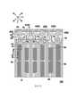
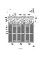
圖1為本發明一實施例之顯示裝置10的俯視示意圖。FIG. 1 is a schematic top view of a
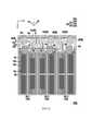
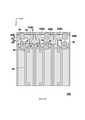
圖2為本發明一實施例之畫素陣列基板100之一區域的俯視示意圖。FIG. 2 is a schematic top view of a region of the
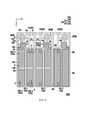
圖3為本發明一實施例之畫素陣列基板100之一區域的俯視示意圖。FIG. 3 is a schematic top view of a region of the
圖4為本發明一實施例之畫素陣列基板100之一區域的俯視示意圖。FIG. 4 is a schematic top view of a region of the
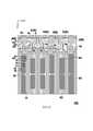
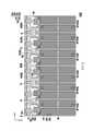
圖5為本發明一實施例之顯示裝置10的剖面示意圖。FIG. 5 is a schematic cross-sectional view of the
圖6為本發明一實施例之畫素陣列基板100A之一區域的俯視示意圖。6 is a schematic top view of a region of a
圖7為本發明一實施例之畫素陣列基板100B之一區域的俯視示意圖。FIG. 7 is a schematic top view of a region of the
圖8為本發明一實施例之畫素陣列基板100B之一區域的俯視示意圖。FIG. 8 is a schematic top view of a region of the
圖9為本發明一實施例之畫素陣列基板100B之一區域的俯視示意圖。FIG. 9 is a schematic top view of a region of the
圖10為本發明一實施例之畫素陣列基板100C之一區域的俯視示意圖。10 is a schematic top view of a region of a
圖11為本發明一實施例之畫素陣列基板100C之一區域的俯視示意圖。11 is a schematic top view of a region of a
圖12為本發明一實施例之畫素陣列基板100C之一區域的俯視示意圖。FIG. 12 is a schematic top view of a region of the
圖13為本發明一實施例之畫素陣列基板100D之一區域的俯視示意圖。FIG. 13 is a top view of a region of the
圖14為本發明一實施例之畫素陣列基板100D之一區域的俯視示意圖。FIG. 14 is a schematic top view of a region of the
圖15為本發明一實施例之畫素陣列基板100D之一區域的俯視示意圖。FIG. 15 is a schematic top view of a region of the
圖16為本發明一實施例之畫素陣列基板100E之一區域的俯視示意圖。FIG. 16 is a schematic top view of a region of the
圖17為本發明一實施例之畫素陣列基板100E之一區域的俯視示意圖。FIG. 17 is a schematic top view of a region of the
圖18為本發明一實施例之畫素陣列基板100E之一區域的俯視示意圖。FIG. 18 is a schematic top view of a region of the
圖19為本發明一實施例之畫素陣列基板100F之一區域的俯視示意圖。FIG. 19 is a schematic top view of a region of the
圖20為本發明一實施例之畫素陣列基板100F之一區域的俯視示意圖。FIG. 20 is a schematic top view of a region of the
圖21為本發明一實施例之畫素陣列基板100F之一區域的俯視示意圖。FIG. 21 is a schematic top view of a region of the
圖22為本發明一實施例之畫素陣列基板100G之一區域的俯視示意圖。FIG. 22 is a schematic top view of a region of the
圖23為本發明一實施例之畫素陣列基板100G之一區域的俯視示意圖。FIG. 23 is a schematic top view of a region of the
圖24為本發明一實施例之畫素陣列基板100G之一區域的俯視示意圖。FIG. 24 is a top view of a region of the
圖25為本發明一實施例之畫素陣列基板100H之一區域的俯視示意圖。FIG. 25 is a schematic top view of a region of the
圖26為本發明一實施例之畫素陣列基板100I之一區域的俯視示意圖。FIG. 26 is a schematic top view of a region of the pixel array substrate 100I according to an embodiment of the present invention.
圖27為本發明一實施例之畫素陣列基板100J之一區域的俯視示意圖。FIG. 27 is a schematic top view of a region of the
現將詳細地參考本發明的示範性實施例,示範性實施例的實例說明於附圖中。只要有可能,相同元件符號在圖式和描述中用來表示相同或相似部分。Reference will now be made in detail to the exemplary embodiments of the present invention, examples of which are illustrated in the accompanying drawings. Wherever possible, the same reference numerals are used in the drawings and description to refer to the same or like parts.
應當理解,當諸如層、膜、區域或基板的元件被稱為在另一元件“上”或“連接到”另一元件時,其可以直接在另一元件上或與另一元件連接,或者中間元件可以也存在。相反,當元件被稱為“直接在另一元件上”或“直接連接到”另一元件時,不存在中間元件。如本文所使用的,“連接”可以指物理及/或電性連接。再者,“電性連接”或“耦合”可以是二元件間存在其它元件。It will be understood that when an element such as a layer, film, region or substrate is referred to as being "on" or "connected to" another element, it can be directly on or connected to the other element, or Intermediate elements may also be present. In contrast, when an element is referred to as being "directly on" or "directly connected to" another element, there are no intervening elements present. As used herein, "connected" may refer to a physical and/or electrical connection. Furthermore, "electrically connected" or "coupled" may refer to the existence of other elements between the two elements.
本文使用的“約”、“近似”、或“實質上”包括所述值和在本領域普通技術人員確定的特定值的可接受的偏差範圍內的平均值,考慮到所討論的測量和與測量相關的誤差的特定數量(即,測量系統的限制)。例如,“約”可以表示在所述值的一個或多個標準偏差內,或±30%、±20%、±10%、±5%內。再者,本文使用的“約”、“近似”或“實質上”可依光學性質、蝕刻性質或其它性質,來選擇較可接受的偏差範圍或標準偏差,而可不用一個標準偏差適用全部性質。As used herein, "about," "approximately," or "substantially" includes the stated value and the average within an acceptable deviation from the particular value as determined by one of ordinary skill in the art, given the measurement in question and the A specified amount of measurement-related error (ie, a limitation of the measurement system). For example, "about" can mean one or more standard deviations in the stated valueWithin the difference, or within ±30%, ±20%, ±10%, ±5%. Furthermore, as used herein, "about", "approximately" or "substantially" may be used to select a more acceptable range of deviation or standard deviation depending on optical properties, etching properties or other properties, and not one standard deviation may apply to all properties. .
除非另有定義,本文使用的所有術語(包括技術和科學術語)具有與本發明所屬領域的普通技術人員通常理解的相同的含義。將進一步理解的是,諸如在通常使用的字典中定義的那些術語應當被解釋為具有與它們在相關技術和本發明的上下文中的含義一致的含義,並且將不被解釋為理想化的或過度正式的意義,除非本文中明確地這樣定義。Unless otherwise defined, all terms (including technical and scientific terms) used herein have the same meaning as commonly understood by one of ordinary skill in the art to which this invention belongs. It will be further understood that terms such as those defined in commonly used dictionaries should be construed as having meanings consistent with their meanings in the context of the related art and the present invention, and are not to be construed as idealized or excessive Formal meaning, unless expressly defined as such herein.
圖1為本發明一實施例之顯示裝置10的俯視示意圖。FIG. 1 is a schematic top view of a
圖2為本發明一實施例之畫素陣列基板100之一區域的俯視示意圖。FIG. 2 is a schematic top view of a region of the
圖3為本發明一實施例之畫素陣列基板100之一區域的俯視示意圖。圖3省略圖2的透明導電層150。FIG. 3 is a schematic top view of a region of the
圖4為本發明一實施例之畫素陣列基板100之一區域的俯視示意圖。圖4省略圖2的多個畫素電極122。FIG. 4 is a schematic top view of a region of the
圖5為本發明一實施例之顯示裝置10的剖面示意圖。圖5對應圖2的剖線I-I’。FIG. 5 is a schematic cross-sectional view of the
請參照圖1、圖2及圖5,顯示裝置10包括畫素陣列基板100、相對於畫素陣列基板100的對向基板200以及設置於畫素陣列基板100與對向基板200之間的顯示介質300。舉例而言,在本實施例中,顯示介質300可以是液晶。然而,本發明不限於此,在其它實施例中,顯示介質300也可以是多個有機電致發光圖案、多個微型發光二極體元件或其它可適用的材料。Referring to FIGS. 1 , 2 and 5 , the
畫素陣列基板100包括基底110。基底110用以承載畫素陣列基板100的多個構件。舉例而言,在本實施例中,基底110的材質可以是玻璃。然而,本發明不限於此,根據其它實施例,基底110的材質也可以是石英、有機聚合物、或是不透光/反射材料(例如:晶圓、陶瓷等)、或是其它可適用的材料。The
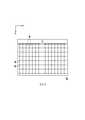
畫素陣列基板100包括多條資料線DL和多條閘極線GL,設置於基底110上。多條資料線DL在第一方向x上排列,多條閘極線GL第二方向y上排列,其中第一方向x與第二方向y交錯。舉例而言,在本實施例中,第一方向x與第二方向y可垂直,但本發明不以此為限。The
資料線DL與閘極線GL屬於不同的膜層。舉例而言,在本實施例中,閘極線GL可選擇性地屬於第一金屬層,資料線DL可選擇性地屬於第二金屬層,但本發明不以此為限。The data line DL and the gate line GL belong to different layers. For example, in this embodiment, the gate line GL can selectively belong to the first metal layer, and the data line DL can selectively belong to the second metal layer, but the invention is not limited thereto.
基於導電性的考量,在本實施例中,資料線DL與閘極線GL是使用金屬材料。然而,本發明不限於此,根據其他實施例,資料線DL與閘極線GL也可以使用其他導電材料,例如:合金、金屬材料的氮化物、金屬材料的氧化物、金屬材料的氮氧化物、或是金屬材料與其它導電材料的堆疊層。Based on the consideration of conductivity, in this embodiment, the data line DL and the gate line GL are made of metal materials. However, the present invention is not limited to this. According to other embodiments, the data line DL and the gate line GL can also use other conductive materials, such as alloys, nitrides of metal materials, oxides of metal materials, and oxynitrides of metal materials. , or a stack of metal materials and other conductive materials.
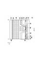
畫素陣列基板100更包括多個畫素結構120,設置於基底110上。每一畫素結構120包括一主動元件121及電性連接至主動元件121的一畫素電極122,且主動元件121電性連接至對應的一條資料線DL及對應的一條閘極線GL。The
舉例而言,在本實施例中,主動元件121包括一薄膜電晶體,薄膜電晶體具有源極121a、汲極121b、閘極121c及半導體圖案121d,絕緣層130夾設於閘極121c與半導體圖案121d之間,源極121a和汲極121b分別與半導體圖案121d的不同兩區電性連接,源極121a電性連接至對應的一條資料線DL,閘極121c電性連接至對應的一條閘極線GL,且汲極121b電性連接至畫素電極122。For example, in this embodiment, the
請參照圖2及圖3,在本實施例中,畫素電極122可選擇性地具有多個狹縫122s,以定義畫素結構120的至少一配向區R。舉例而言,在本實施例中,畫素電極122可選擇性包括一第一主幹部122a、一第二主幹部122b及多個第一分支部122c;第一主幹部122a與第二主幹部122b相交錯,以劃分多個配向區R;在同一配向區R中,多個第一分支部122c朝同一方向延伸且彼此隔開,以定義多個狹縫122s;但本發明不以此為限。Referring to FIG. 2 and FIG. 3 , in this embodiment, the
在本實施例中,畫素電極122所在的一子畫素區可選擇性包括四個配向區R。然而,本發明不限於此,在另一實施例中,一子畫素區也可具有其它數量(例如:一個、二個、三個或五個以上)的配向區R。此外,在另一實施例中,畫素電極122也可不具有狹縫122s。In this embodiment, a sub-pixel region where the
請參照圖2及圖5,在本實施例中,畫素陣列基板100更包括共用線CL,設置於基底110上,其中多條資料線DL及共用線CL在第一方向x上排列。共用線CL可與畫素電極122部分地重疊,以形成一儲存電容。2 and FIG. 5 , in this embodiment, the
在本實施例中,閘極121c和閘極線GL可選擇性地屬於第一金屬層,源極121a、汲極121b、資料線DL及共用線CL可選擇性地屬於第二金屬層,畫素陣列基板100還可包括設置於第二金屬層上的絕緣層140,畫素電極122可設置於絕緣層140上且透過絕緣層140的貫孔140a電性連接至薄膜電晶體的汲極121b,但本發明不以此為限。In this embodiment, the
在本實施例中,畫素電極122例如是透光的,透光之畫素電極122的材質可包括金屬氧化物,例如:銦錫氧化物、銦鋅氧化物、鋁錫氧化物、鋁鋅氧化物、銦鍺鋅氧化物、其它合適的氧化物、或者是上述至少二者之堆疊層。需說明的是,本發明並不限制畫素電極122一定要透光;在其它實施例中,畫素電極122也可反光、或部分反光且部分透光。In this embodiment, the
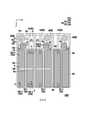
請參照圖1及圖2,畫素陣列基板100還包括多條轉接線gl,設置於基底110上,且在第一方向x上排列。在第一方向x上排列的多條轉接線gl電性連接至在第二方向y上排列的多條閘極線GL,並穿插於多個畫素結構120之間。Referring to FIG. 1 and FIG. 2 , the
舉例而言,在本實施例中,閘極線GL可選擇性地屬於第一金屬層,且轉接線gl可選擇性地屬於第二金屬層。然而,本發明不以此為限,在其它實施例中,轉接線gl也可包括分別屬於第一金屬層及第二金屬層的多個部分。For example, in this embodiment, the gate line GL can selectively belong to the first metal layer, and the transition line gl can selectively belong to the second metal layer. However, the presentIt is not limited to this, and in other embodiments, the patch wire gl may also include a plurality of parts respectively belonging to the first metal layer and the second metal layer.
請參照圖2、圖3及圖4,多個畫素結構120包括第一畫素結構120-1,多條資料線DL包括電性連接至第一畫素結構120-1的第一資料線DL1,且多條轉接線gl包括第一轉接線gl1。第一資料線DL1具有一第一部DLa,設置於第一畫素結構120-1的畫素電極122外,且位於第一畫素結構120-1的主動元件121旁。2, 3 and 4, the plurality of
每一畫素結構120的主動元件121具有相對的第一側(例如但不限於:左側)及第二側(例如但不限於:右側)。值得注意的是,在畫素陣列基板100的俯視圖中,第一畫素結構120-1的主動元件121具有相對的第一側(例如但不限於:左側)及第二側(例如但不限於:右側),第一轉接線gl1設置於第一畫素結構120-1之主動元件121的第一側(例如但不限於:左側),且第一資料線DL1的第一部DLa及共用線CL設置於第一畫素結構120-1之主動元件121的第二側(例如但不限於:右側)。換言之,當一畫素結構120的相對兩側分別設有轉接線gl及共用線CL時,資料線DL之繞過主動元件121的一部分(即第一部DLa)是設置在較靠近共用線CL且遠離轉接線gl之處。藉此,可減少資料線DL與轉接線gl之間的耦合電容,降低轉接線gl之訊號變化對畫素電極122之電位的影響,進而改善顯示品質。The
請參照圖2,在畫素陣列基板100的俯視圖中,第一資料線DL1的第一部DLa與第一轉接線gl1在第一方向x上具有第一距離D1,第一資料線DL1的第一部DLa與共用線CL在第一方向x上具有第二距離D2,且第一距離D1大於第二距離D2。Referring to FIG. 2 , in the top view of the
請參照圖2,在本實施例中,多個畫素結構120更包括第二畫素結構120-2,第一畫素結構120-1與第二畫素結構120-2相鄰設置且在第一方向x上排列;多條資料線DL更包括電性連接至第二畫素結構120-2的第二資料線DL2;多條轉接線gl更包括第二轉接線gl2;第二資料線DL2具有第一部DLa,設置於第二畫素結構120-2的畫素電極122外,且位於第二畫素結構120-2的主動元件121旁。Referring to FIG. 2 , in this embodiment, the plurality of
在畫素陣列基板100的俯視圖中,第二畫素結構120-2的主動元件121具有相對的第一側(例如但不限於:左側)及第二側(例如但不限於:右側),共用線CL及第二資料線DL2的第一部DLa設置於第二畫素結構120-2之主動元件121的第一側(例如但不限於:左側),且第二轉接線gl2設置於第二畫素結構120-2之主動元件121的第二側(例如但不限於:右側)。換言之,當一畫素結構120的相對兩側分別設有共用線CL及轉接線gl時,資料線DL之繞過主動元件121的一部分(即第一部DLa)是設置在較靠近共用線CL且遠離轉接線gl之處。藉此,可減少資料線DL與轉接線gl之間的耦合電容,降低轉接線gl之訊號變化對畫素電極122之電位的影響,進而改善顯示品質。In the top view of the
在畫素陣列基板100的俯視圖中,第二資料線DL2的第一部DLa與共用線CL在第一方向x上具有第三距離D3,第二資料線DL2的第一部DLa與第二轉接線gl2在第一方向x上具有第四距離D4,且第四距離D4大於第三距離D3。In the top view of the
請參照圖2,在本實施例中,多個畫素結構120更包括第三畫素結構120-3,第一畫素結構120-1、第二畫素結構120-2及第三畫素結構120-3在第一方向x上依序排列;第一畫素結構120-1、第二畫素結構120-2及第三畫素結構120-3之間沒有其它畫素結構120;多條資料線DL更包括電性連接至第三畫素結構120-3的第三資料線DL3;多條轉接線gl更包括第三轉接線gl3;第三資料線DL3具有第一部DLa,設置於第三畫素結構120-3的畫素電極122外,且位於第三畫素結構120-3的主動元件121旁。Referring to FIG. 2 , in this embodiment, the plurality of
在畫素陣列基板100的俯視圖中,第三畫素結構120-3的主動元件121具有相對的第一側(例如但不限於:左側)及第二側(例如但不限於:右側),第二轉接線gl2及第三資料線DL3的第一部DLa設置於第三畫素結構120-3之主動元件121的第一側(例如但不限於:左側),且第三轉接線gl3設置於第三畫素結構120-3之主動元件121的第二側(例如但不限於:右側)。當一畫素結構120的相對兩側均設有轉接線gl時,資料線DL之繞過主動元件121的一部分(即第一部DLa)可任意地設置在較靠近其中一條轉接線gl之處。In the top view of the
在本實施例中,第三畫素結構120-3用以顯示藍色。換言之,其相對兩側均設有轉接線gl的畫素結構120是以用來顯示藍色為佳。藉此,能減少轉接線gl對顯示品質造成的不良影響。此外,在本實施例中,第一畫素結構120-1及第二畫素結構120-2例如是分別用以顯示紅色及綠色,但本發明不以此為限。In this embodiment, the third pixel structure 120-3 is used to display blue. In other words, the
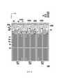
請參照圖2、圖4及圖5,在本實施例中,畫素陣列基板100更包括透明導電層150,其中資料線DL、透明導電層150及畫素結構120的畫素電極122在垂直於基底110的第三方向z上堆疊,且透明導電層150設置於資料線DL與畫素結構120的畫素電極122之間。此外,在本實施例中,共用線CL、透明導電層150及畫素結構120之畫素電極122在垂直於基底110的第三方向z上堆疊,且透明導電層150設置於共用線CL與畫素結構120的畫素電極122之間。Referring to FIGS. 2 , 4 and 5 , in this embodiment, the
簡言之,在本實施例中,透明導電層150是設置在畫素電極122所屬的膜層與第二金屬層之間,以對第二金屬層之構件(例如但不限於:轉接線gl)造成一屏蔽效應;藉此,能降低第二金屬層之構件(例如但不限於:轉接線gl)的訊號對畫素電極122造成的不良影響,進而改善顯示品質。In short, in the present embodiment, the transparent
在本實施例中,透明導電層150的電位與共用線CL的電位實質上可相等。在本實施例中,對向基板200除了基底210外可選擇性地包括設置於基底210上的一共用電極220(繪示於圖5),共用電極220重疊於多個畫素結構120的多個畫素電極122,顯示介質300設置於共用電極220與多個畫素電極122之間,共用電極220與每一畫素電極122之間的電位差可用以驅動顯示介質300,進而使顯示裝置10能顯示畫面。在本實施例中,畫素陣列基板100之透明導電層150的電位與對向基板200之共用電極220的電位實質上可相等,但本發明不以此為限。In this embodiment, the potential of the transparent
在本實施例中,畫素陣列基板100可選擇性地更包括一彩色濾光圖案層160(標示於圖5),其中彩色濾光圖案層160設置於絕緣層140上,而透明導電層150設置於彩色濾光圖案層160上;畫素陣列基板100更包括一絕緣層170,絕緣層170設置透明導電層150上,而畫素電極122設置於絕緣層170上。In this embodiment, the
請參照圖2及圖4,值得注意的是,在本實施例中,透明導電層150可具有多個開口152,重疊於畫素結構120的畫素電極122。透明導電層150之多個開口152有助於減少透明導電層150對畫素電極122所形成之電場的干擾,進而增加液晶效率、提升顯示裝置10的穿透率。Please refer to FIG. 2 and FIG. 4 , it should be noted that, in this embodiment, the transparent
在本實施例中,透明導電層150具有與資料線DL重疊的一第一實體部151;在畫素陣列基板100的俯視圖中,透明導電層150的第一實體部151具有定義多個開口152的一邊緣151e,且透明導電層150之第一實體部151的邊緣151e位於資料線DL外。換言之,雖然透明導電層150具有多個開口152,但透明導電層150的第一實體部151仍良好地遮蔽資料線DL與畫素電極122重疊的第二部DLb。In this embodiment, the transparent
舉例而言,在本實施例中,在畫素陣列基板100的俯視圖中,透明導電層150之第一實體部151的邊緣151e與資料線DL的邊緣DLe具有一最小距離W,且最小距離W大於或等於5μm且小於或等於8μm,但本發明不以此為限。For example, in this embodiment, in the top view of the
請參照圖2、圖3及圖4,在本實施例中,在畫素陣列基板100的俯視圖中,畫素電極122的多個狹縫122s設置於第一範圍RG1,透明導電層150的多個開口152設置於第二範圍RG2,第一範圍RG1及第二範圍RG2重疊,且第二範圍RG2的面積小於第一範圍RG1的面積。Referring to FIGS. 2 , 3 and 4 , in the present embodiment, in the top view of the
在本實施例中,畫素結構120的畫素電極122具有多個第一分支部122c,多個第一分支部122c彼此隔開以定義多個狹縫122s,一第一分支部122c具有第一線寬L1,多個第一分支部122c的相鄰兩者具有一第一間距S1;透明導電層150具有多個第二分支部153,多個第二分支部153彼此隔開以定義多個開口152,一第二分支部153具有第二線寬L2,多個第二分支部153的相鄰兩者具有一第二間距S2;透明導電層150之第二線寬L2及第二間距S2的和大於畫素電極122之第一線寬L1與第一間距S1的和。In this embodiment, the
在本實施例中,在畫素陣列基板100的俯視圖中,透明導電層150的多個開口152位於資料線DL的相對兩側。在本實施例中,畫素電極122的多個狹縫122s包括多個狹縫122s-1、多個狹縫122s-2、多個狹縫122s-3及多個狹縫122s-4,分別設置於由畫素電極122之第一主幹部122a及第二主幹部122b劃分的多個配向區R;透明導電層150的多個開口152可包括多個開口152-1、多個開口152-2、多個開口152-3及多個開口152-4,分別重疊於畫素電極122的多個狹縫122s-1、多個狹縫122s-2、多個狹縫122s-3及多個狹縫122s-4。In this embodiment, in the top view of the
在本實施例中,透明導電層150的多個開口152-1、152-2、152-3或152-4可在第一方向x上排列。在本實施例中,透明導電層150的多個開口152可在第二方向y上延伸。換言之,在本實施例中,透明導電層150的多個開口152可以是直向開口。然而,本發明不以此為限,在其它實施例中,多個開口152也可以是其它形狀及/或以其它方式設置,以下配合其它圖式舉例說明之。In this embodiment, the plurality of openings 152-1, 152-2, 152-3 or 152-4 of the transparent
在此必須說明的是,下述實施例沿用前述實施例的元件標號與部分內容,其中採用相同的標號來表示相同或近似的元件,並且省略了相同技術內容的說明。關於省略部分的說明可參考前述實施例,下述實施例不再重述。It must be noted here that the following embodiments use the element numbers and part of the contents of the previous embodiments, wherein the same numbers are used to represent the same or similar elements, and the description of the same technical contents is omitted. For the description of the omitted part, reference may be made to the foregoing embodiments, and the following embodiments will not be repeated.
圖6為本發明一實施例之畫素陣列基板100A之一區域的俯視示意圖。6 is a schematic top view of a region of a
圖6的畫素陣列基板100A與圖2的畫素陣列基板100類似,兩者的差異在於:在圖2實施例中,第三資料線DL3的第一部DLa是設置於第三畫素結構120-3之主動元件121的第一側(例如但不限於:左側);但在圖6實施例中,第三資料線DL3的第一部DLa是設置於第三畫素結構120-3之主動元件121的第二側(例如但不限於:右側)。The
圖7為本發明一實施例之畫素陣列基板100B之一區域的俯視示意圖。FIG. 7 is a schematic top view of a region of the
圖8為本發明一實施例之畫素陣列基板100B之一區域的俯視示意圖。圖8省略圖7的透明導電層150。FIG. 8 is a view of a region of the
圖9為本發明一實施例之畫素陣列基板100B之一區域的俯視示意圖。圖9省略圖7的畫素電極122。FIG. 9 is a schematic top view of a region of the
圖7至圖9的畫素陣列基板100B與圖2至圖4的畫素陣列基板100類似,兩者主要的差異在於:兩者之透明導電層150的開口152不同。The
請參照圖7至圖9,具體而言,在本實施例中,透明導電層150的多個開口152在第二方向y上排列。透明導電層150的每一開口152可在第一方向x上延伸。換言之,在本實施例中,透明導電層150的多個開口152可以是多個橫向開口。Please refer to FIG. 7 to FIG. 9 . Specifically, in this embodiment, the plurality of
圖10為本發明一實施例之畫素陣列基板100C之一區域的俯視示意圖。10 is a schematic top view of a region of a
圖11為本發明一實施例之畫素陣列基板100C之一區域的俯視示意圖。圖11省略圖10的透明導電層150。11 is a schematic top view of a region of a
圖12為本發明一實施例之畫素陣列基板100C之一區域的俯視示意圖。圖12省略圖10的畫素電極122。FIG. 12 is a schematic top view of a region of the
圖10至圖12的畫素陣列基板100C與圖2至圖4的畫素陣列基板100類似,兩者主要的差異在於:兩者之透明導電層150的開口152不同。The
請參照圖10至圖12,具體而言,在本實施例中,透明導電層150具有多個第二分支部153C-1、153C-2,彼此交錯呈網狀,以定義多個開口152(標示於圖12)。更進一步地說,在本實施例中,多個第二分支部153C-1、153C-2可包括彼此交錯的多個第二分支部153C-1及多個第二分支部153C-2,其中多個第二分支部153C-1可選擇性地平行於資料線DL的第二部DLb,且多個第二分支部153C-1可選擇性地垂直於資料線DL的第二部DLb。Please refer to FIGS. 10 to 12 . Specifically, in this embodiment, the transparent
圖13為本發明一實施例之畫素陣列基板100D之一區域的俯視示意圖。FIG. 13 is a schematic top view of a region of the
圖14為本發明一實施例之畫素陣列基板100D之一區域的俯視示意圖。圖14省略圖13的透明導電層150。FIG. 14 is a schematic top view of a region of the
圖15為本發明一實施例之畫素陣列基板100D之一區域的俯視示意圖。圖15省略圖13的畫素電極122。FIG. 15 is a schematic top view of a region of the
圖13至圖15的畫素陣列基板100D與圖2至圖4的畫素陣列基板100類似,兩者主要的差異在於:兩者之透明導電層150的開口152不同。The
請參照圖13至圖15,具體而言,在本實施例中,多條資料線DL在第一方向x上排列,多條閘極線GL在第二方向y上排列,透明導電層150的多個開口152在第四方向d4上排列,且第一方向x、第二方向y及第四方向d4互不相同。Please refer to FIGS. 13 to 15 . Specifically, in this embodiment, a plurality of data lines DL are arranged in the first direction x, and a plurality of gate lines GL are arranged in the second direction y. The plurality of
更進一步地說,在本實施例中,畫素結構120的畫素電極122具有多個狹縫122s,畫素電極122的多個狹縫122s重疊於透明導電層150的多個開口152,畫素電極122的多個狹縫122s在第五方向d5上排列,透明導電層150的多個開口152在第四方向d4上排列,且第四方向d4與第五方向d5實質上相同。More specifically, in this embodiment, the
圖16為本發明一實施例之畫素陣列基板100E之一區域的俯視示意圖。FIG. 16 is a schematic top view of a region of the
圖17為本發明一實施例之畫素陣列基板100E之一區域的俯視示意圖。圖17省略圖16的透明導電層150。FIG. 17 is a schematic top view of a region of the
圖18為本發明一實施例之畫素陣列基板100E之一區域的俯視示意圖。圖18省略圖16的畫素電極122。FIG. 18 is a schematic top view of a region of the
圖16至圖18的畫素陣列基板100E與圖13至圖15的畫素陣列基板100D類似,兩者主要的差異在於:兩者之透明導電層150的開口152不同。The
請參照圖16至圖18,具體而言,在本實施例中,畫素電極122的多個狹縫122s在第五方向d5上排列,透明導電層150的多個開口152在第四方向d4上排列,且第四方向d4與第五方向d5夾有一角度θ,且0°<θ
圖19為本發明一實施例之畫素陣列基板100F之一區域的俯視示意圖。FIG. 19 is a schematic top view of a region of the
圖20為本發明一實施例之畫素陣列基板100F之一區域的俯視示意圖。圖20省略圖19的透明導電層150。FIG. 20 is a schematic top view of a region of the
圖21為本發明一實施例之畫素陣列基板100F之一區域的俯視示意圖。圖21省略圖19的畫素電極122。FIG. 21 is a schematic top view of a region of the
圖19至圖21的畫素陣列基板100F與圖10至圖12的畫素陣列基板100類似,兩者主要的差異在於:兩者之透明導電層150的開口152不同。The
請參照圖19至圖21,類似地,在本實施例中,透明導電層150具有多個第二分支部153C-1、153C-2(標示於圖21),彼此交錯呈網狀,以定義多個開口152;透明導電層150的多個第二分支部153C-1、153C-2可包括彼此交錯的多個第二分支部153C-1及多個第二分支部153C-2。與圖10至圖12之實施例不同的是,在本實施例中,多個第二分支部153C-1不平行也不垂直於資料線DL的第二部DLb,且多個第二分支部153C-1不平行也不垂直於資料線DL的第二部DLb。簡言之,在本實施例中,透明導電層150的多個第二分支部153C-1、153C-2可交織成斜向設置的網狀圖案。Referring to FIGS. 19 to 21 , similarly, in this embodiment, the transparent
圖22為本發明一實施例之畫素陣列基板100G之一區域的俯視示意圖。FIG. 22 is a schematic top view of a region of the
圖23為本發明一實施例之畫素陣列基板100G之一區域的俯視示意圖。圖23省略圖22的透明導電層150。FIG. 23 is a schematic top view of a region of the
圖24為本發明一實施例之畫素陣列基板100G之一區域的俯視示意圖。圖24省略圖22的畫素電極122。FIG. 24 is a schematic top view of a region of the
圖22至圖24的畫素陣列基板100G與圖2至圖4的畫素陣列基板100類似,兩者主要的差異在於:兩者之透明導電層150的開口152不同。The
請參照圖22至圖24,在本實施例中,透明導電層150不具有前述畫素陣列基板100的開口152,透明導電層150的實體可與畫素電極122重疊。Referring to FIGS. 22 to 24 , in this embodiment, the transparent
圖25為本發明一實施例之畫素陣列基板100H之一區域的俯視示意圖。圖25的畫素陣列基板100H與圖2的畫素陣列基板100類似,以下說明兩者主要的差異,兩者相同或相似處請參照前述說明,於此便不再重述。FIG. 25 is a schematic top view of a region of the
請參照圖25,在本實施例中,多個畫素結構120更包括第四畫素結構120-4;第一畫素結構120-1與第四畫素結構120-4分別設置於第一轉接線gl1的相對兩側;多條資料線DL更包括電性連接至第四畫素結構120-4的第四資料線DL4;第四資料線DL4具有第一部DLa,設置於第四畫素結構120-4的畫素電極122外,且位於第四畫素結構120-4的主動元件121旁。特別是,在畫素陣列基板100H的俯視圖中,第一資料線DL1的第一部DLa設置於第一畫素結構120-1之主動元件121的第二側(例如但不限於:右側),且第四資料線DL4的第一部DLa設置於第四畫素結構120-4之主動元件121的第一側(例如但不限於:右側)。也就是說,在本實施例中,有兩個畫素結構120相鄰於同一條轉接線gl且分別位於同一條轉接線gl的相對兩側,而分別電性連接至所述兩個畫素結構120的兩條資料線DL的兩個第一部DLa均設置在遠離所述轉接線gl處。Referring to FIG. 25 , in this embodiment, the plurality of
請參照圖25,在本實施例中,第一畫素結構120-1及第四畫素結構120-4分別用以顯示紅色及藍色。也就是說,在畫素陣列基板100的俯視圖中,一轉接線gl設置於分別用以顯示紅色及藍色的多個畫素結構120之間。Referring to FIG. 25, in this embodiment, the first pixel structure 120-1 and the fourth pixel structure 120-4 are used to display red and blue, respectively. That is, in the top view of the
請參照圖25,在本實施例中,多個畫素結構120更包括第五畫素結構120-5及、第六畫素結構120-6、第七畫素結構120-7及第八畫素結構120-8。第七畫素結構120-7、第八畫素結構120-8、第四畫素結構120-4、第一畫素結構120-1、第五畫素結構120-5及第六畫素結構120-6在第一方向x上依序排列。第七畫素結構120-7、第八畫素結構120-8、第四畫素結構120-4、第一畫素結構120-1、第五畫素結構120-5及第六畫素結構120-6分別用以顯示紅色、綠色、藍色、紅色、綠色及藍色。多條資料線DL更包括電性連接至第五畫素結構120-5的第五資料線DL5。第五資料線DL5具有第一部DLa,設置於第五畫素結構120-5的畫素電極122外,且位於第五畫素結構120-5的主動元件121旁。多條資料線DL更包括電性連接至第六畫素結構120-6的第六資料線DL6。第六資料線DL6具有第一部DLa,設置於第六畫素結構120-6的畫素電極122外,且位於第六畫素結構120-6的主動元件121旁。Referring to FIG. 25 , in this embodiment, the plurality of
特別是,在畫素陣列基板100H的俯視圖中,第五資料線DL5的第一部DLa設置於第五畫素結構120-5之主動元件121的第二側(例如但不限於:右側),且第六資料線DL6的第一部DLa設置於第六畫素結構120-6之主動元件121的第一側(例如但不限於:左側)。也就是說,分別電性連接至用以顯示綠色及藍色之兩個畫素結構120的兩條資料線DL的兩第一部DLa係相鄰設置。In particular, in the top view of the
圖26為本發明一實施例之畫素陣列基板100I之一區域的俯視示意圖。圖26的畫素陣列基板100I與圖25的畫素陣列基板100H類似,兩者的差異在於:在圖26之畫素陣列基板100I的俯視圖中,第一資料線DL1的第一部DLa設置於第一畫素結構120-1之主動元件121的第二側(例如但不限於:右側),且第五資料線DL5的第一部DLa設置於第五畫素結構120-5之主動元件121的第一側(例如但不限於:左側)。也就是說,在圖26的實施例中,分別電性連接至用以顯示紅色及綠色之兩個畫素結構120之兩條資料線DL的兩第一部DLa係相鄰設置。FIG. 26 is a schematic top view of a region of the pixel array substrate 100I according to an embodiment of the present invention. The pixel array substrate 100I of FIG. 26 and the pixel array substrate of FIG. 25100H is similar, the difference between the two is: in the top view of the pixel array substrate 100I of FIG. 26 , the first portion DLa of the first data line DL1 is disposed on the second side of the
圖27為本發明一實施例之畫素陣列基板100J之一區域的俯視示意圖。圖27的畫素陣列基板100J與圖2的畫素陣列基板100類似,以下說明兩者主要的差異,兩者相同或相似處請參照前述說明,於此便不再重述。FIG. 27 is a schematic top view of a region of the
請參照圖27,在本實施例中,第一畫素結構120-1及第二畫素結構120-2分別設置於第一轉接線gl1的相對兩側。多條資料線DL包括第一資料線DL1及第二資料線DL2,分別電性連接至第一畫素結構120-1及第二畫素結構120-2。第一資料線DL1具有第一部DLa,設置於第一畫素結構120-1的畫素電極122外,且位於第一畫素結構120-1的主動元件121旁。第二資料線DL2具有第一部DLa,設置於第二畫素結構120-2的畫素電極122外,且位於第二畫素結構120-2的主動元件121旁。Referring to FIG. 27 , in this embodiment, the first pixel structure 120 - 1 and the second pixel structure 120 - 2 are respectively disposed on opposite sides of the first patch wire gl1 . The plurality of data lines DL include a first data line DL1 and a second data line DL2, which are electrically connected to the first pixel structure 120-1 and the second pixel structure 120-2, respectively. The first data line DL1 has a first portion DLa, disposed outside the
特別是,在畫素陣列基板100J的俯視圖中,第一轉接線gl1設置於第一畫素結構120-1之主動元件121的第一側(例如但不限於:左側),第一資料線DL1的第一部DLa設置於第一畫素結構120-1之主動元件121的第二側(例如但不限於:右側),第一轉接線gl1設置於第二畫素結構120-2之主動元件121的第二側(例如但不限於:右側),且第二資料線DL2的第一部DLa設置於第二畫素結構120-2之主動元件121的第一側(例如但不限於:左側)。也就是說,在本實施例中,有兩個畫素結構120相鄰於同一條轉接線g1且分別位於同一條轉接線g1的相對兩側,而分別電性連接至所述兩個畫素結構120的兩條資料線DL的兩個第一部DLa均設置在遠離所述轉接線gl處。In particular, in the top view of the
請參照圖27,在本實施例中,多個畫素結構120更包括第九畫素結構120-9、第十畫素結構120-10、第十一畫素結構120-11及第十二畫素結構120-12。第十一畫素結構120-11、第十二畫素結構120-12、第二畫素結構120-2、第一畫素結構120-1、第九畫素結構120-9及第十畫素結構120-10在第一方向x上依序排列。第十一畫素結構120-11、第十二畫素結構120-12、第二畫素結構120-2、第一畫素結構120-1、第九畫素結構120-9及第十畫素結構120-10可分別用以顯示紅色、綠色、藍色、紅色、綠色及藍色。Referring to FIG. 27 , in this embodiment, the plurality of
此外,圖27之畫素陣列基板100J不包括圖2之畫素陣列基板100的共用線CL,而包括共用電極CL’。請參照圖27,在本實施例中,共用電極CL’包括至少一第一部CL’-1,共用電極CL’的至少一第一部CL’-1與閘極線GL在第二方向y上排列,且共用電極CL’的至少一第一部CL’-1與畫素電極122部分地重疊。在本實施例中,共用電極CL’更包括至少一第二部CL’-2,共用電極CL’的至少一第二部CL’-2與資料線DL在第一方向x上排列,且共用電極CL’的至少一第二部CL’-2與畫素電極122部分地重疊。再者,圖27之畫素陣列基板100J可不包括圖2之畫素陣列基板100的透明導電層150。In addition, the
100: 畫素陣列基板 120: 畫素結構 120-1: 第一畫素結構 120-2: 第二畫素結構 120-3: 第三畫素結構 121: 主動元件 121a: 源極 121b: 汲極 121c: 閘極 121d: 半導體圖案 122: 畫素電極 122s: 狹縫 150: 透明導電層 152: 開口 CL: 共用線 D1: 第一距離 D2: 第二距離 D3: 第三距離 D4: 第四距離 DL: 資料線 DL1: 第一資料線 DL2: 第二資料線 DL3: 第三資料線 DLa: 第一部 DLb: 第二部 GL: 閘極線 gl: 轉接線 gl1: 第一轉接線 gl2: 第二轉接線 gl3: 第三轉接線 x: 第一方向 y: 第二方向 І-І’: 剖線100: Pixel Array Substrate 120: Pixel Structure 120-1: First Pixel Structure 120-2: Second Pixel Structure 120-3: Third Pixel Structure 121:
Claims (24)
Translated fromChinese
Priority Applications (3)
| Application Number | Priority Date | Filing Date | Title |
|---|---|---|---|
| CN202121490248.2UCN215183965U (en) | 2020-08-03 | 2021-07-01 | Pixel array substrate |
| CN202411508369.3ACN119451226A (en) | 2020-08-03 | 2021-07-01 | Pixel array substrate |
| CN202110745303.6ACN114068584B (en) | 2020-08-03 | 2021-07-01 | Pixel array substrate |
Applications Claiming Priority (2)
| Application Number | Priority Date | Filing Date | Title |
|---|---|---|---|
| US202063060259P | 2020-08-03 | 2020-08-03 | |
| US63/060,259 | 2020-08-03 |
Publications (2)
| Publication Number | Publication Date |
|---|---|
| TW202207189A TW202207189A (en) | 2022-02-16 |
| TWI757071Btrue TWI757071B (en) | 2022-03-01 |
Family
ID=79907572
Family Applications (5)
| Application Number | Title | Priority Date | Filing Date |
|---|---|---|---|
| TW110100967ATWI759066B (en) | 2020-08-03 | 2021-01-11 | Pixel array substrate |
| TW110100968ATWI747707B (en) | 2020-08-03 | 2021-01-11 | Pixel array substrate |
| TW110103109ATWI757071B (en) | 2020-08-03 | 2021-01-27 | Pixel array substrate |
| TW110103827ATWI757081B (en) | 2020-08-03 | 2021-02-02 | Pixel array substrate |
| TW110115718ATWI781603B (en) | 2020-08-03 | 2021-04-30 | Touch panel |
Family Applications Before (2)
| Application Number | Title | Priority Date | Filing Date |
|---|---|---|---|
| TW110100967ATWI759066B (en) | 2020-08-03 | 2021-01-11 | Pixel array substrate |
| TW110100968ATWI747707B (en) | 2020-08-03 | 2021-01-11 | Pixel array substrate |
Family Applications After (2)
| Application Number | Title | Priority Date | Filing Date |
|---|---|---|---|
| TW110103827ATWI757081B (en) | 2020-08-03 | 2021-02-02 | Pixel array substrate |
| TW110115718ATWI781603B (en) | 2020-08-03 | 2021-04-30 | Touch panel |
Country Status (2)
| Country | Link |
|---|---|
| CN (1) | CN114068585B (en) |
| TW (5) | TWI759066B (en) |
Families Citing this family (1)
| Publication number | Priority date | Publication date | Assignee | Title |
|---|---|---|---|---|
| TWI802393B (en)* | 2022-05-03 | 2023-05-11 | 友達光電股份有限公司 | Pixel array substrate |
Citations (2)
| Publication number | Priority date | Publication date | Assignee | Title |
|---|---|---|---|---|
| CN104252073A (en)* | 2013-06-27 | 2014-12-31 | 瀚宇彩晶股份有限公司 | touch LCD display |
| TW201641993A (en)* | 2015-05-28 | 2016-12-01 | Toppan Printing Co Ltd | Liquid crystal display device |
Family Cites Families (27)
| Publication number | Priority date | Publication date | Assignee | Title |
|---|---|---|---|---|
| JP2007079367A (en)* | 2005-09-16 | 2007-03-29 | Seiko Epson Corp | Electro-optical device and electronic apparatus including the same |
| JP2009103797A (en)* | 2007-10-22 | 2009-05-14 | Hitachi Displays Ltd | Liquid crystal display device |
| TWI392943B (en)* | 2009-01-08 | 2013-04-11 | Au Optronics Corp | Display device having slim border-area architecture and driving method thereof |
| CN102081246A (en)* | 2009-12-01 | 2011-06-01 | 群康科技(深圳)有限公司 | Liquid crystal display panel and liquid crystal display device |
| JP2011186239A (en)* | 2010-03-09 | 2011-09-22 | Toshiba Mobile Display Co Ltd | Liquid crystal display device |
| CN102819361B (en)* | 2011-06-08 | 2016-04-27 | 比亚迪股份有限公司 | Capacitance touch screen and there is its contactor control device |
| TWI505334B (en)* | 2012-01-05 | 2015-10-21 | E Ink Holdings Inc | Pixel array substrate and display panel using the same |
| JP6056175B2 (en)* | 2012-04-03 | 2017-01-11 | セイコーエプソン株式会社 | Electro-optical device and electronic apparatus |
| US9646559B2 (en)* | 2012-08-10 | 2017-05-09 | Lg Display Co., Ltd. | Liquid crystal display device |
| KR101906248B1 (en)* | 2012-12-13 | 2018-10-11 | 엘지디스플레이 주식회사 | Liquid crystal display device |
| TWI495110B (en)* | 2013-03-22 | 2015-08-01 | Au Optronics Corp | Display panel and method of making the same |
| KR102321635B1 (en)* | 2014-08-14 | 2021-11-08 | 삼성디스플레이 주식회사 | Touch screen panel |
| JP2016071082A (en)* | 2014-09-29 | 2016-05-09 | パナソニック液晶ディスプレイ株式会社 | Display device |
| JP2016114779A (en)* | 2014-12-15 | 2016-06-23 | 株式会社ジャパンディスプレイ | Liquid crystal display device |
| CN104977740A (en)* | 2015-07-29 | 2015-10-14 | 京东方科技集团股份有限公司 | Display substrate and preparation method thereof, and display apparatus |
| KR102519516B1 (en)* | 2015-12-18 | 2023-04-06 | 엘지디스플레이 주식회사 | Liquid crystal display device |
| CN106200176A (en)* | 2016-08-25 | 2016-12-07 | 深圳市华星光电技术有限公司 | Display floater and display |
| TWI639110B (en)* | 2017-09-05 | 2018-10-21 | 奇景光電股份有限公司 | Wearable electronic device and a reflected-capacitive touch panel thereof |
| CN107783696B (en)* | 2017-10-16 | 2020-11-03 | 友达光电(苏州)有限公司 | Touch panel |
| JP6768724B2 (en)* | 2018-01-19 | 2020-10-14 | 株式会社Joled | How to drive the display device and display panel |
| CN108594554B (en)* | 2018-05-09 | 2020-11-17 | 京东方科技集团股份有限公司 | Array substrate, driving method thereof and display device |
| TWI677864B (en)* | 2018-06-28 | 2019-11-21 | 友達光電股份有限公司 | Display device |
| CN110570801B (en)* | 2018-12-05 | 2022-12-06 | 友达光电股份有限公司 | Display device |
| KR102512914B1 (en)* | 2018-12-28 | 2023-03-22 | 엘지디스플레이 주식회사 | Display panel, display device, and driving circuit |
| TWI685828B (en)* | 2019-01-03 | 2020-02-21 | 友達光電股份有限公司 | Display apparatus |
| US10852609B2 (en)* | 2019-02-27 | 2020-12-01 | Au Optronics Corporation | Pixel array substrate and driving method thereof |
| CN110825264B (en)* | 2019-10-31 | 2022-10-11 | 厦门天马微电子有限公司 | Display panel, driving method and touch display device |
- 2021
- 2021-01-11TWTW110100967Apatent/TWI759066B/enactive
- 2021-01-11TWTW110100968Apatent/TWI747707B/enactive
- 2021-01-27TWTW110103109Apatent/TWI757071B/enactive
- 2021-02-02TWTW110103827Apatent/TWI757081B/enactive
- 2021-04-30TWTW110115718Apatent/TWI781603B/enactive
- 2021-07-02CNCN202110749131.XApatent/CN114068585B/enactiveActive
Patent Citations (2)
| Publication number | Priority date | Publication date | Assignee | Title |
|---|---|---|---|---|
| CN104252073A (en)* | 2013-06-27 | 2014-12-31 | 瀚宇彩晶股份有限公司 | touch LCD display |
| TW201641993A (en)* | 2015-05-28 | 2016-12-01 | Toppan Printing Co Ltd | Liquid crystal display device |
Also Published As
| Publication number | Publication date |
|---|---|
| TWI781603B (en) | 2022-10-21 |
| TW202207189A (en) | 2022-02-16 |
| CN114068585B (en) | 2025-08-29 |
| TWI759066B (en) | 2022-03-21 |
| CN114068585A (en) | 2022-02-18 |
| TW202207000A (en) | 2022-02-16 |
| TW202207443A (en) | 2022-02-16 |
| TW202207202A (en) | 2022-02-16 |
| TW202206920A (en) | 2022-02-16 |
| TWI747707B (en) | 2021-11-21 |
| TWI757081B (en) | 2022-03-01 |
Similar Documents
| Publication | Publication Date | Title |
|---|---|---|
| US9588385B2 (en) | Liquid crystal display and manufacturing method thereof | |
| CN1530724A (en) | Four-color liquid crystal display and panel for the same | |
| CN101504503A (en) | Pixel array, liquid crystal display panel and photoelectric device | |
| WO2022193337A1 (en) | Array substrate and display panel | |
| TWI708105B (en) | Pixel array substrate | |
| WO2020088279A1 (en) | Display substrate and display device | |
| CN113050335A (en) | Array substrate, display panel and display device | |
| WO2023070726A1 (en) | Array substrate and display panel | |
| TWI757071B (en) | Pixel array substrate | |
| CN215183965U (en) | Pixel array substrate | |
| TWI628497B (en) | Pixel structure | |
| US11289044B2 (en) | Display device | |
| CN110646988A (en) | Display device | |
| CN113782543B (en) | Pixel array substrate | |
| CN110058461A (en) | Liquid crystal display device with electrode stack | |
| TWI714322B (en) | Pixel array substrate and driving method thereof | |
| CN223296247U (en) | Array substrate, display panel and display device | |
| CN118712202B (en) | Display panel | |
| CN219658710U (en) | display device | |
| TWI754554B (en) | Pixel array substrate | |
| CN222800969U (en) | Display panel and display device | |
| TWI764516B (en) | Pixel array substrate | |
| US20250006747A1 (en) | Display substrate and display device | |
| US20250271708A1 (en) | Display panel | |
| TWI716676B (en) | Display panel |