TWI756234B - Selective etch using material modification and rf pulsing - Google Patents
Selective etch using material modification and rf pulsingDownload PDFInfo
- Publication number
- TWI756234B TWI756234BTW106121039ATW106121039ATWI756234BTW I756234 BTWI756234 BTW I756234BTW 106121039 ATW106121039 ATW 106121039ATW 106121039 ATW106121039 ATW 106121039ATW I756234 BTWI756234 BTW I756234B
- Authority
- TW
- Taiwan
- Prior art keywords
- plasma
- power supply
- semiconductor substrate
- pulsed
- processing chamber
- Prior art date
Links
Images


Classifications
- H—ELECTRICITY
- H01—ELECTRIC ELEMENTS
- H01L—SEMICONDUCTOR DEVICES NOT COVERED BY CLASS H10
- H01L21/00—Processes or apparatus adapted for the manufacture or treatment of semiconductor or solid state devices or of parts thereof
- H01L21/02—Manufacture or treatment of semiconductor devices or of parts thereof
- H01L21/04—Manufacture or treatment of semiconductor devices or of parts thereof the devices having potential barriers, e.g. a PN junction, depletion layer or carrier concentration layer
- H01L21/18—Manufacture or treatment of semiconductor devices or of parts thereof the devices having potential barriers, e.g. a PN junction, depletion layer or carrier concentration layer the devices having semiconductor bodies comprising elements of Group IV of the Periodic Table or AIIIBV compounds with or without impurities, e.g. doping materials
- H01L21/30—Treatment of semiconductor bodies using processes or apparatus not provided for in groups H01L21/20 - H01L21/26
- H01L21/31—Treatment of semiconductor bodies using processes or apparatus not provided for in groups H01L21/20 - H01L21/26 to form insulating layers thereon, e.g. for masking or by using photolithographic techniques; After treatment of these layers; Selection of materials for these layers
- H01L21/3105—After-treatment
- H01L21/3115—Doping the insulating layers
- H—ELECTRICITY
- H01—ELECTRIC ELEMENTS
- H01L—SEMICONDUCTOR DEVICES NOT COVERED BY CLASS H10
- H01L21/00—Processes or apparatus adapted for the manufacture or treatment of semiconductor or solid state devices or of parts thereof
- H01L21/67—Apparatus specially adapted for handling semiconductor or electric solid state devices during manufacture or treatment thereof; Apparatus specially adapted for handling wafers during manufacture or treatment of semiconductor or electric solid state devices or components ; Apparatus not specifically provided for elsewhere
- H01L21/67005—Apparatus not specifically provided for elsewhere
- H01L21/67011—Apparatus for manufacture or treatment
- H01L21/67017—Apparatus for fluid treatment
- H01L21/67063—Apparatus for fluid treatment for etching
- H01L21/67069—Apparatus for fluid treatment for etching for drying etching
- H—ELECTRICITY
- H01—ELECTRIC ELEMENTS
- H01L—SEMICONDUCTOR DEVICES NOT COVERED BY CLASS H10
- H01L21/00—Processes or apparatus adapted for the manufacture or treatment of semiconductor or solid state devices or of parts thereof
- H01L21/02—Manufacture or treatment of semiconductor devices or of parts thereof
- H01L21/04—Manufacture or treatment of semiconductor devices or of parts thereof the devices having potential barriers, e.g. a PN junction, depletion layer or carrier concentration layer
- H01L21/18—Manufacture or treatment of semiconductor devices or of parts thereof the devices having potential barriers, e.g. a PN junction, depletion layer or carrier concentration layer the devices having semiconductor bodies comprising elements of Group IV of the Periodic Table or AIIIBV compounds with or without impurities, e.g. doping materials
- H01L21/30—Treatment of semiconductor bodies using processes or apparatus not provided for in groups H01L21/20 - H01L21/26
- H01L21/302—Treatment of semiconductor bodies using processes or apparatus not provided for in groups H01L21/20 - H01L21/26 to change their surface-physical characteristics or shape, e.g. etching, polishing, cutting
- H01L21/306—Chemical or electrical treatment, e.g. electrolytic etching
- H01L21/3065—Plasma etching; Reactive-ion etching
- H—ELECTRICITY
- H01—ELECTRIC ELEMENTS
- H01J—ELECTRIC DISCHARGE TUBES OR DISCHARGE LAMPS
- H01J37/00—Discharge tubes with provision for introducing objects or material to be exposed to the discharge, e.g. for the purpose of examination or processing thereof
- H01J37/32—Gas-filled discharge tubes
- H01J37/32009—Arrangements for generation of plasma specially adapted for examination or treatment of objects, e.g. plasma sources
- H01J37/32082—Radio frequency generated discharge
- H01J37/32137—Radio frequency generated discharge controlling of the discharge by modulation of energy
- H01J37/32146—Amplitude modulation, includes pulsing
- H—ELECTRICITY
- H01—ELECTRIC ELEMENTS
- H01J—ELECTRIC DISCHARGE TUBES OR DISCHARGE LAMPS
- H01J37/00—Discharge tubes with provision for introducing objects or material to be exposed to the discharge, e.g. for the purpose of examination or processing thereof
- H01J37/32—Gas-filled discharge tubes
- H01J37/32009—Arrangements for generation of plasma specially adapted for examination or treatment of objects, e.g. plasma sources
- H01J37/32082—Radio frequency generated discharge
- H01J37/32174—Circuits specially adapted for controlling the RF discharge
- H—ELECTRICITY
- H01—ELECTRIC ELEMENTS
- H01J—ELECTRIC DISCHARGE TUBES OR DISCHARGE LAMPS
- H01J37/00—Discharge tubes with provision for introducing objects or material to be exposed to the discharge, e.g. for the purpose of examination or processing thereof
- H01J37/32—Gas-filled discharge tubes
- H01J37/32431—Constructional details of the reactor
- H01J37/32697—Electrostatic control
- H01J37/32706—Polarising the substrate
- H—ELECTRICITY
- H01—ELECTRIC ELEMENTS
- H01L—SEMICONDUCTOR DEVICES NOT COVERED BY CLASS H10
- H01L21/00—Processes or apparatus adapted for the manufacture or treatment of semiconductor or solid state devices or of parts thereof
- H01L21/02—Manufacture or treatment of semiconductor devices or of parts thereof
- H01L21/04—Manufacture or treatment of semiconductor devices or of parts thereof the devices having potential barriers, e.g. a PN junction, depletion layer or carrier concentration layer
- H01L21/18—Manufacture or treatment of semiconductor devices or of parts thereof the devices having potential barriers, e.g. a PN junction, depletion layer or carrier concentration layer the devices having semiconductor bodies comprising elements of Group IV of the Periodic Table or AIIIBV compounds with or without impurities, e.g. doping materials
- H01L21/30—Treatment of semiconductor bodies using processes or apparatus not provided for in groups H01L21/20 - H01L21/26
- H01L21/31—Treatment of semiconductor bodies using processes or apparatus not provided for in groups H01L21/20 - H01L21/26 to form insulating layers thereon, e.g. for masking or by using photolithographic techniques; After treatment of these layers; Selection of materials for these layers
- H01L21/3105—After-treatment
- H01L21/311—Etching the insulating layers by chemical or physical means
- H01L21/31105—Etching inorganic layers
- H01L21/31111—Etching inorganic layers by chemical means
- H01L21/31116—Etching inorganic layers by chemical means by dry-etching
- H—ELECTRICITY
- H01—ELECTRIC ELEMENTS
- H01L—SEMICONDUCTOR DEVICES NOT COVERED BY CLASS H10
- H01L21/00—Processes or apparatus adapted for the manufacture or treatment of semiconductor or solid state devices or of parts thereof
- H01L21/67—Apparatus specially adapted for handling semiconductor or electric solid state devices during manufacture or treatment thereof; Apparatus specially adapted for handling wafers during manufacture or treatment of semiconductor or electric solid state devices or components ; Apparatus not specifically provided for elsewhere
- H01L21/683—Apparatus specially adapted for handling semiconductor or electric solid state devices during manufacture or treatment thereof; Apparatus specially adapted for handling wafers during manufacture or treatment of semiconductor or electric solid state devices or components ; Apparatus not specifically provided for elsewhere for supporting or gripping
- H01L21/6831—Apparatus specially adapted for handling semiconductor or electric solid state devices during manufacture or treatment thereof; Apparatus specially adapted for handling wafers during manufacture or treatment of semiconductor or electric solid state devices or components ; Apparatus not specifically provided for elsewhere for supporting or gripping using electrostatic chucks
- H01L21/6833—Details of electrostatic chucks
- H—ELECTRICITY
- H01—ELECTRIC ELEMENTS
- H01L—SEMICONDUCTOR DEVICES NOT COVERED BY CLASS H10
- H01L21/00—Processes or apparatus adapted for the manufacture or treatment of semiconductor or solid state devices or of parts thereof
- H01L21/67—Apparatus specially adapted for handling semiconductor or electric solid state devices during manufacture or treatment thereof; Apparatus specially adapted for handling wafers during manufacture or treatment of semiconductor or electric solid state devices or components ; Apparatus not specifically provided for elsewhere
- H01L21/683—Apparatus specially adapted for handling semiconductor or electric solid state devices during manufacture or treatment thereof; Apparatus specially adapted for handling wafers during manufacture or treatment of semiconductor or electric solid state devices or components ; Apparatus not specifically provided for elsewhere for supporting or gripping
- H01L21/687—Apparatus specially adapted for handling semiconductor or electric solid state devices during manufacture or treatment thereof; Apparatus specially adapted for handling wafers during manufacture or treatment of semiconductor or electric solid state devices or components ; Apparatus not specifically provided for elsewhere for supporting or gripping using mechanical means, e.g. chucks, clamps or pinches
- H01L21/68714—Apparatus specially adapted for handling semiconductor or electric solid state devices during manufacture or treatment thereof; Apparatus specially adapted for handling wafers during manufacture or treatment of semiconductor or electric solid state devices or components ; Apparatus not specifically provided for elsewhere for supporting or gripping using mechanical means, e.g. chucks, clamps or pinches the wafers being placed on a susceptor, stage or support
- H01L21/68735—Apparatus specially adapted for handling semiconductor or electric solid state devices during manufacture or treatment thereof; Apparatus specially adapted for handling wafers during manufacture or treatment of semiconductor or electric solid state devices or components ; Apparatus not specifically provided for elsewhere for supporting or gripping using mechanical means, e.g. chucks, clamps or pinches the wafers being placed on a susceptor, stage or support characterised by edge profile or support profile
- H—ELECTRICITY
- H05—ELECTRIC TECHNIQUES NOT OTHERWISE PROVIDED FOR
- H05H—PLASMA TECHNIQUE; PRODUCTION OF ACCELERATED ELECTRICALLY-CHARGED PARTICLES OR OF NEUTRONS; PRODUCTION OR ACCELERATION OF NEUTRAL MOLECULAR OR ATOMIC BEAMS
- H05H1/00—Generating plasma; Handling plasma
- H05H1/24—Generating plasma
- H05H1/46—Generating plasma using applied electromagnetic fields, e.g. high frequency or microwave energy
- H—ELECTRICITY
- H01—ELECTRIC ELEMENTS
- H01J—ELECTRIC DISCHARGE TUBES OR DISCHARGE LAMPS
- H01J2237/00—Discharge tubes exposing object to beam, e.g. for analysis treatment, etching, imaging
- H01J2237/32—Processing objects by plasma generation
- H01J2237/33—Processing objects by plasma generation characterised by the type of processing
- H01J2237/334—Etching
- H—ELECTRICITY
- H01—ELECTRIC ELEMENTS
- H01L—SEMICONDUCTOR DEVICES NOT COVERED BY CLASS H10
- H01L21/00—Processes or apparatus adapted for the manufacture or treatment of semiconductor or solid state devices or of parts thereof
- H01L21/02—Manufacture or treatment of semiconductor devices or of parts thereof
- H01L21/04—Manufacture or treatment of semiconductor devices or of parts thereof the devices having potential barriers, e.g. a PN junction, depletion layer or carrier concentration layer
- H01L21/18—Manufacture or treatment of semiconductor devices or of parts thereof the devices having potential barriers, e.g. a PN junction, depletion layer or carrier concentration layer the devices having semiconductor bodies comprising elements of Group IV of the Periodic Table or AIIIBV compounds with or without impurities, e.g. doping materials
- H01L21/30—Treatment of semiconductor bodies using processes or apparatus not provided for in groups H01L21/20 - H01L21/26
- H01L21/31—Treatment of semiconductor bodies using processes or apparatus not provided for in groups H01L21/20 - H01L21/26 to form insulating layers thereon, e.g. for masking or by using photolithographic techniques; After treatment of these layers; Selection of materials for these layers
- H01L21/3105—After-treatment
Landscapes
- Engineering & Computer Science (AREA)
- Physics & Mathematics (AREA)
- Condensed Matter Physics & Semiconductors (AREA)
- General Physics & Mathematics (AREA)
- Manufacturing & Machinery (AREA)
- Computer Hardware Design (AREA)
- Microelectronics & Electronic Packaging (AREA)
- Power Engineering (AREA)
- Chemical & Material Sciences (AREA)
- Plasma & Fusion (AREA)
- Analytical Chemistry (AREA)
- Chemical Kinetics & Catalysis (AREA)
- General Chemical & Material Sciences (AREA)
- Inorganic Chemistry (AREA)
- Electromagnetism (AREA)
- Spectroscopy & Molecular Physics (AREA)
- Drying Of Semiconductors (AREA)
- Plasma Technology (AREA)
Abstract
Description
Translated fromChinese本技術關於用於處理半導體材料的系統及方法。更具體而言,本技術關於用於產生低電力電漿的半導體材料變性及硬體變性。The present technology relates to systems and methods for processing semiconductor materials. More specifically, the present technology relates to semiconductor material denaturation and hardware denaturation for generating low power plasma.
可能藉由在基板表面上產生錯綜複雜地佈局的材料層的製程來製作積體電路。在基板上產生經佈局的材料的步驟需要用於施用及移除材料的受控方法。對於移除而言,化學蝕刻用於各種用途,包括將光阻劑中的圖樣轉移進下層的層、薄化的層或已經存在於表面上的薄化的特徵側向尺度。通常想要擁有較另一材料為快地蝕刻一個材料而例如促進圖樣轉移製程的蝕刻製程。此類蝕刻製程被稱為對於第一材料是有選擇性的。材料、電路及製程的多樣性的結果是,已研發了對於各種材料具有選擇性的蝕刻製程。Integrated circuits may be fabricated by processes that create intricately arranged layers of material on the surface of a substrate. The step of producing the laid-out material on the substrate requires a controlled method for applying and removing the material. For removal, chemical etching is used for a variety of purposes, including transferring patterns in photoresist into underlying layers, thinned layers, or thinned feature lateral dimensions already present on the surface. It is often desirable to have an etch process that etches one material faster than another, such as to facilitate pattern transfer processes. Such an etching process is said to be selective to the first material. As a result of the diversity of materials, circuits, and processes, etching processes that are selective for various materials have been developed.
可基於製程中所使用的材料而將蝕刻製程稱為是濕的或乾的。濕的HF蝕刻相較於其他介電質及材料而言優先移除氧化矽。然而,濕製程可能在穿透某些受限的溝時有困難,且亦可能有時使其餘材料變形。在基板處理區域內所形成之局部電漿中所產生的乾蝕刻可穿透更加受限的溝且展現了較少的精巧的其餘結構的變形。然而,局部的電漿可能在它們放電時經由產生電弧而損傷基板。此外,電漿溢流可能損傷可能需要替換或處理的腔室元件。The etch process can be referred to as wet or dry based on the materials used in the process. Wet HF etch preferentially removes silicon oxide over other dielectrics and materials. However, the wet process may have difficulty penetrating certain confined trenches and may also sometimes deform the remaining material. The dry etch created in the localized plasma formed in the substrate processing region can penetrate more confined trenches and exhibit less deformation of the delicate rest of the structure. However, localized plasmas can damage substrates by creating arcs as they discharge. Additionally, plasma flooding can damage chamber components that may require replacement or disposal.
因此,存在著可用以產生高品質設備及結構的改良的系統及方法的需要。本技術解決這些及其他的需要。Accordingly, there is a need for improved systems and methods that can be used to produce high quality devices and structures. The present technology addresses these and other needs.
半導體系統及方法可包括執行選擇性蝕刻的方法,該等方法包括以下步驟:使一半導體基板上的一材料變性。該基板可在該半導體基板的一表面上具有至少兩種受暴材料。該等方法可包括以下步驟:在收容該半導體基板的一處理腔室內形成一低電力電漿。該低電力電漿可為一射頻(「RF」)電漿,該射頻電漿在實施例中可至少部分地由一RF偏壓電源所形成,該RF偏壓電源在約10 W及約100 W之間運作。該RF偏壓電源亦可使用低於約5,000 Hz的一頻率發出脈衝。該等方法亦可包括以下步驟:相較於該半導體基板之該表面上之該至少兩種受暴材料中的一第二種材料以一較高的蝕刻速率蝕刻該半導體基板之該表面上之該至少兩種受暴材料中的一種受暴材料。Semiconductor systems and methods can include methods of performing selective etching, the methods including the steps of denaturing a material on a semiconductor substrate. The substrate may have at least two exposed materials on a surface of the semiconductor substrate. The methods may include the steps of forming a low power plasma within a processing chamber housing the semiconductor substrate. The low power plasma may be a radio frequency ("RF") plasma, which in embodiments may be formed at least in part by an RF bias power supply between about 10 W and about 100 Works between W. The RF bias power supply can also be pulsed using a frequency below about 5,000 Hz. The methods may also include the step of etching a second material on the surface of the semiconductor substrate at a higher etch rate than a second material of the at least two exposed materials on the surface of the semiconductor substrate A blasted material of the at least two blasted materials.
在實施例中,該變性操作可包括以該RF偏壓電源從該處理腔室內的一母材形成一電漿。在實施例中,該母材可選自由以下所組成之群組:氧、氫或氦。此外,該半導體基板之該表面上之該至少兩種受暴材料中的各者可選自由以下所組成之群組:氧化矽、氮化矽、碳化矽及碳氧化矽。In embodiments, the denaturing operation may include forming a plasma from a parent material within the processing chamber with the RF bias power supply. In an embodiment, the parent material can be selected from the group consisting of oxygen, hydrogen or helium. Additionally, each of the at least two exposed materials on the surface of the semiconductor substrate may be selected from the group consisting of silicon oxide, silicon nitride, silicon carbide, and silicon oxycarbide.
對於蝕刻操作而言,該RF偏壓電源可至少部分地形成該低電力電漿且低於約50%的一工作週期下運作。並且,形成該低電力電漿的步驟可更包括利用低於約100 W的一RF源電源。在實施例中,形成該低電力電漿的步驟亦可包括利用一脈衝式DC電源。該脈衝式DC電源可施用於支撐該半導體基板的一雙極靜電夾具。在實施例中,該脈衝式DC電源可施用於一導電環,該導電環嵌在支撐該半導體基板之一托架的一罩環中或與該處理腔室內的一蓮蓬頭耦合。For etching operations, the RF bias power supply may at least partially form the low power plasma and operate at a duty cycle of less than about 50%. Also, the step of forming the low power plasma may further include utilizing an RF source power below about 100 W. In an embodiment, the step of forming the low power plasma may also include utilizing a pulsed DC power supply. The pulsed DC power supply can be applied to a bipolar electrostatic fixture supporting the semiconductor substrate. In embodiments, the pulsed DC power supply may be applied to a conductive ring embedded in a shroud ring supporting a carrier of the semiconductor substrate or coupled to a showerhead within the processing chamber.
本技術亦包括了從一半導體基板移除材料的方法。該等方法可包括以下步驟:使一半導體基板上的一材料變性,該半導體基板在該半導體基板的一表面上具有至少兩種受暴材料。該變性步驟可包括:以一RF偏壓電源從一母材形成一電漿以生成使該材料變性的電漿溢流。該等方法亦可包括以下步驟:在收容該半導體基板的一處理腔室內形成一低電力電漿。該低電力電漿在實施例中可為一射頻(RF)電漿。該低電力電漿可藉由一脈衝式RF偏壓電源來形成,該脈衝式RF偏壓電源在約500 Hz及約2,000 Hz之間的一脈衝頻率下在約20 W及50 W之間下運作。該脈衝式RF偏壓電源亦可在約20%及50%之間的一工作週期下運作。該等方法可包括以下步驟:與該RF偏壓電源脈衝在一交流頻率上操作一DC脈衝式電源。該等方法可更包括以下步驟:相對於該半導體基板之該表面上之該至少兩種受暴材料中的一第二種材料以至少約20:1的一選擇性蝕刻該半導體基板之該表面上之該至少兩種受暴材料中的一種受暴材料。The present technology also includes methods of removing material from a semiconductor substrate. The methods may include the step of denaturing a material on a semiconductor substrate having at least two exposed materials on a surface of the semiconductor substrate. The denaturing step may include forming a plasma from a parent material with an RF bias power source to generate a plasma flood that denatures the material. The methods may also include the step of forming a low power plasma in a processing chamber containing the semiconductor substrate. The low power plasma may be a radio frequency (RF) plasma in an embodiment. The low power plasma can be formed by a pulsed RF bias power supply at between about 20 W and 50 W at a pulse frequency between about 500 Hz and about 2,000 Hz operate. The pulsed RF bias power supply can also operate at a duty cycle between about 20% and 50%. The methods may include the steps of operating a DC pulsed power supply at an AC frequency with the RF bias power supply pulses. The methods may further include the step of etching the surface of the semiconductor substrate with a selectivity of at least about 20:1 to a second material of the at least two exposed materials on the surface of the semiconductor substrate One of the at least two exposed materials above.
在該等方法中,該變性操作包括一化學變性,該化學變性對於該半導體基板上的該材料造成一化學變化。該變性步驟亦可包括利用一惰性母材的一物理變性。在實施例中,該物理變性可包括以該惰性母材的離子損傷該半導體基板上之該材料的鍵結。形成該低電力電漿的該操作可更包括利用以最多約100 W運作的一RF源電源。In these methods, the denaturation operation includes a chemical denaturation that causes a chemical change to the material on the semiconductor substrate. The denaturation step may also include a physical denaturation using an inert parent material. In an embodiment, the physical denaturation can include damaging bonds of the material on the semiconductor substrate with ions of the inert parent material. The operation of forming the low power plasma may further include utilizing an RF source power operating at a maximum of about 100 W.
本技術亦包括了基板處理腔室,該等基板處理腔室包括被配置為支撐一半導體基板的一托架。在實施例中,該等腔室可包括一RF偏壓電源,該RF偏壓電源與該托架電耦合且被配置為以約20 W及約50 W之間的一功率在該處理腔室內生成一電漿。該RF偏壓電源可為被配置為使用低於約5,000 Hz的一頻率發出脈衝的一脈衝電源。該等基板處理腔室可更包括:一DC脈衝電源,與該基板處理腔室電耦合,且被配置為產生用於該RF偏壓電漿的引火粒子。此外,該DC脈衝電源供應器可被配置為在不發展一電漿鞘的情況下以一頻率發出脈衝以產生引火粒子。The present technology also includes substrate processing chambers that include a carriage configured to support a semiconductor substrate. In embodiments, the chambers may include an RF bias power supply electrically coupled to the carrier and configured to operate within the processing chamber at a power of between about 20 W and about 50 W A plasma is generated. The RF bias power supply may be a pulsed power supply configured to pulse using a frequency below about 5,000 Hz. The substrate processing chambers may further include: a DC pulsed power supply electrically coupled to the substrate processing chambers and configured to generate pyrophoric particles for the RF bias plasma. Additionally, the DC pulsed power supply can be configured to pulse at a frequency to generate ignition particles without developing a plasma sheath.
在實施例中,該DC脈衝電源供應器可被配置為在小於約50%的一工作週期下啟動脈衝100微秒或更少的一持續時間。此外,在實施例中,該托架可為一雙極靜電夾具,且該DC脈衝電源可施用於該雙極靜電夾具的電接地。在實施例中,該DC脈衝電源可與一導電環電耦合,該導電環與該托架耦合,且該導電環可與該靜電夾具及該RF偏壓電解耦。在實施例中,該DC脈衝電源亦可與一導電環電耦合,該導電環嵌在該基板處理腔室內的一蓮蓬頭中。In an embodiment, the DC pulsed power supply may be configured to enable pulses for a duration of 100 microseconds or less at a duty cycle of less than about 50%. Additionally, in embodiments, the carrier may be a bipolar electrostatic clamp, and the DC pulsed power source may be applied to the electrical ground of the bipolar electrostatic clamp. In an embodiment, the DC pulsed power supply can be electrically coupled to a conductive ring, the conductive ring is coupled to the carrier, and the conductive ring can be decoupled from the electrostatic clamp and the RF bias. In an embodiment, the DC pulsed power supply can also be electrically coupled to a conductive ring embedded in a showerhead within the substrate processing chamber.
此類技術相對於傳統的技術可提供許多益處。例如,該技術可例如由於材料變性而允許改良的蝕刻操作選擇性。此外,本技術的低電力電漿相對於傳統的技術可產生改良的特徵剖面,且允許在使用強化的電漿控制的情況下進行改良的前端及後端處理。與以下說明及隨附圖式結合來更詳細地描述這些及其他實施例以及許多它們的優點及特徵。Such techniques can provide many benefits over conventional techniques. For example, this technique may allow for improved selectivity of etching operations, eg, due to material denaturation. In addition, the low power plasma of the present technology can produce improved feature profiles relative to conventional technologies, and allow for improved front-end and back-end processing with enhanced plasma control. These and other embodiments, and many of their advantages and features, are described in greater detail in conjunction with the following description and accompanying drawings.
在半導體處理中,可基於許多理由而執行蝕刻。在乾式蝕刻中,母材可流過電漿而產生用於蝕刻各種半導體材料的自由基電漿溢流。電漿溢流包括了被導向要蝕刻之基板表面及材料的離子。在某些蝕刻操作中(例如在使用反應性離子蝕刻法的情況下),離子被導向材料表面,且基於所涉及的能量可從基板表面濺散材料。基於較第二材料為快地移除一個材料的目標而設計了其他的蝕刻操作(通常稱為選擇性蝕刻)。為了強化選擇性,一個方法可包括以下步驟:減少蝕刻操作的濺散成分。這可部分地藉由減少電漿電力以減少電子溫度來達成。選擇性可能隨著特徵尺寸減少而變得越來越關鍵。選擇性越高,越少的要維持的材料可形成為用於最終產品之目標尺度的緩衝劑。甚至傳統較高的選擇性可能隨著尺寸持續減少而是不適合的。例如,即使從要維持的材料移除數奈米,設備效能亦可能被負面影響。In semiconductor processing, etching can be performed for a number of reasons. In dry etching, the parent material can flow through a plasma to create a radical plasma flood that is used to etch various semiconductor materials. Plasma flooding includes ions directed towards the substrate surface and material to be etched. In certain etching operations (eg, where reactive ion etching is used), ions are directed to the surface of the material, and based on the energy involved, the material can be sputtered from the surface of the substrate. Other etching operations (often referred to as selective etching) are designed with the goal of removing one material faster than the second material. To enhance selectivity, a method may include the step of reducing the sputter component of the etching operation. This can be achieved in part by reducing plasma power to reduce electron temperature. Selectivity may become increasingly critical as feature size decreases. The higher the selectivity, the less material to maintain can be formed as a buffer at the target scale for the final product. Even traditionally higher selectivities may be unsuitable as size continues to decrease. For example, device performance may be negatively impacted even if several nanometers are removed from the material to be maintained.
可以許多方式產生電漿,例如包括使用電連接至支撐基板之托架的射頻(「RF」)偏壓。此偏壓電源可與跟腔室的部分耦合的RF源結合使用或替代該RF源,或可與電感耦合的電漿源、電容耦合的電漿源、微波源或可額外地用以產生電漿溢流的任何其他電漿源結合工作。藉由替代或附加於源電源而利用偏壓電源,可向離子提供方向性以提供更多的異向性的或取決於定向的蝕刻。然而,隨著離子能量增加,濺散亦可能增加。因為濺散可能是更材料獨立的,這可能減少材料之間的選擇性,在該等材料中只有一個材料是要被移除的。據此,目標可能是減少偏壓方的電漿電力以減少濺散以改良選擇性。The plasma can be generated in a number of ways, including, for example, using radio frequency ("RF") biasing of a carrier electrically connected to the support substrate. This bias supply can be used in conjunction with or in place of an RF source coupled to part of the chamber, or can be used in addition to an inductively coupled plasma source, a capacitively coupled plasma source, a microwave source, or in addition to generating electricity Works in conjunction with any other plasma source of plasma overflow. By utilizing a bias power supply in place of or in addition to the source power supply, directionality can be provided to the ions to provide more anisotropic or orientation-dependent etching. However, as ion energy increases, sputtering may also increase. This may reduce the selectivity between materials of which only one is to be removed, as the sputtering may be more material independent. Accordingly, the goal may be to reduce the plasma power on the bias side to reduce sputtering to improve selectivity.
傳統的技術可減少來源或偏壓處的電漿電力,但從使電漿放電的觀點來看以及在產生蝕刻時,該等傳統技術皆在可減少偏壓電力的程度上是受限的。為了使電漿放電,電力必須超過電漿所從以產生之流體的崩潰電壓。對於傳統的濺散及脈衝式蝕刻操作而言,生輝放電通常例如產生在低電流、中電壓工作狀態的500 V周圍及數千瓦特的功率處。然而,這些電力位準將提供增加的離子能量及伴生的材料濺散,這可能導致較低的選擇性。若降低電漿電力以進一步減少濺散,則可能根本難以產生或維持電漿,特別是在使用脈衝式電漿電力的情況下。此外,若偏壓電力被減少太多,則雖然可解決濺散,整體的蝕刻可能被減少至零。Conventional techniques can reduce the plasma power at the source or bias, but they are limited in the extent to which they can reduce the bias power from a plasma discharge standpoint and when creating an etch. In order for the plasma to discharge, the electrical power must exceed the breakdown voltage of the fluid from which the plasma is produced. For conventional sputtering and pulsed etching operations, glow discharges are typically generated, for example, around 500 V for low current, medium voltage operation and at powers of several kilowatts. However, these power levels will provide increased ion energy and concomitant material sputtering, which may result in lower selectivity. If the plasma power is reduced to further reduce sputtering, it may be difficult to generate or maintain the plasma at all, especially if pulsed plasma power is used. Furthermore, if the bias power is reduced too much, the overall etch may be reduced to zero, although spatter can be resolved.
本技術藉由產生脈衝式的低電力RF電漿而克服了許多這些問題。可在高達數百瓦特的源電源下及在百萬赫茲範圍中的脈衝頻率下產生傳統的所謂的低電力電漿。這些電力範圍不能夠產生本技術的選擇性,因為這些電漿的濺散成分仍太明顯。另一方面來說,本技術可在使用低於100瓦特運作之脈衝式RF徧壓的情況下在各種腔室條件下、在低達約20%的工作週期下及在低達約500 Hz的脈衝頻率下產生電漿。在此運作工作狀態下,可減少或實質消除濺散,且可產生可能相較於傳統技術高達一個數量級改良的蝕刻選擇性。本技術可涉及透過材料變性來強化選擇性及執行低電力蝕刻的組合。這些製程可藉由減少要維持的材料量來強化整體選擇性,減少要維持的材料量的步驟是皆藉由減少與其他材料相關的蝕刻量以及減少可能負面地濺散或影響材料的任何電漿效應來進行的。The present technology overcomes many of these problems by generating a pulsed low power RF plasma. Conventional so-called low-power plasma can be generated at source power up to several hundred watts and at pulse frequencies in the megahertz range. These power ranges do not yield the selectivity of the present technology because the sputtering component of these plasmas is still too pronounced. On the other hand, the present technology can operate under various chamber conditions, at duty cycles as low as about 20%, and at frequencies as low as about 500 Hz using pulsed RF pressures operating below 100 watts. Plasma is generated at the pulse frequency. Under this operating state, sputtering can be reduced or substantially eliminated, and etch selectivity that can be improved by as much as an order of magnitude over conventional techniques can result. The present techniques may involve a combination of enhancing selectivity through material denaturation and performing low power etching. These processes can enhance overall selectivity by reducing the amount of material to maintain, both by reducing the amount of etch associated with other materials and reducing any electrical energy that may negatively sputter or affect the material. Slurry effect.
雖然以下說明將例行地識別蝕刻操作,要瞭解的是,本技術可被更廣泛地應用。該等系統及操作方法可被額外應用於沉積、清潔或可能受益於所述之低電力電漿的任何其他電漿操作。據此,本說明書不是要將應用僅限制在本說明書各處所述的實例。While the following description will routinely identify etching operations, it is to be understood that the present techniques can be applied more broadly. The systems and methods of operation can additionally be applied to deposition, cleaning, or any other plasma operation that may benefit from the low power plasma described. Accordingly, this specification is not intended to limit application to only the examples described throughout this specification.
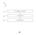
圖1繪示依據本技術的實施例來蝕刻基板的方法100。可在所指出的方法操作之前執行可選的操作,包括佈局、薄膜形成或各種其他習知的製程操作。該方法可包括以下步驟:在操作110處使半導體基板上的材料變性。基板可在半導體基板的表面上具有至少兩種受暴的材料,且可具有三種、四種、五種、六種或更多種不同的受暴材料。此外,一或更多種材料可在選擇性蝕刻方法100之前一開始被覆蓋,但接著被操作暴露,且因此受暴薄膜中的一或更多者可在實施例中的蝕刻操作期間受暴。在實施例中,可試圖移除這些材料中的一或更多者。FIG. 1 illustrates a
該方法亦可包括以下步驟:在操作120處在收容半導體基板的處理腔室內形成低電力電漿。低電力電漿在實施例中可為射頻(「RF」)電漿,然而亦可類似地包括其他的電漿形成方法。低電力電漿在實施例中可藉由在約10 W及100 W之間下運作的RF偏壓電源來至少部分地形成。在實施例中,RF偏壓電源可為脈衝式的,且可在低於約5,000 Hz的脈衝頻率下運作。該方法可更包括以下步驟:在操作130處蝕刻半導體基板表面上之該至少兩個受暴材料中的一或更多者。在實施例中,蝕刻該至少兩個受暴材料中的一或更多者的步驟相較於半導體基板表面上之該至少兩個受暴材料中的第二種材料可處於較高的速率。The method may also include the step of forming a low power plasma in the processing chamber housing the semiconductor substrate at
變性操作可基於基板表面上的材料以任何數量的方式調諧,且可基於材料性質的識別及該等材料與基板表面上的其他材料是如何地不同。例如,變性操作一開始可識別密度、化學結構、反應本性上的差異或薄膜之間可利用的任何其他特徵。可執行材料中的一或更多者的變性以強化或產生薄膜之間可在蝕刻操作中利用的差異。可在實施例中藉由將材料暴露於一或更多種母材來執行變性。在實施例中,母材可或可不在與受暴材料交互作用之前被激發。在實施例中,變性步驟可包括從處理腔室內的母材形成電漿。取決於被變性的薄膜,電漿可在約50 W到約300 W之間。例如,展現較高密度的薄膜在實施例中可受益於較高的電漿電力。可在實施例中以源電源或偏壓電源以及以兩者的組合來產生電漿,以產生使受暴材料中的一或更多者變性的電漿溢流。在實施例中,可以RF偏壓電源形成電漿。Denaturation operations can be tuned in any number of ways based on the materials on the substrate surface, and can be based on identification of material properties and how those materials differ from other materials on the substrate surface. For example, a denaturation operation can initially identify differences in density, chemical structure, nature of reactions, or any other feature that can be exploited between films. Denaturation of one or more of the materials can be performed to strengthen or create differences between thin films that can be exploited in etching operations. Denaturation may be performed in embodiments by exposing the material to one or more parent materials. In embodiments, the parent material may or may not be excited prior to interaction with the exposed material. In an embodiment, the denaturing step may include forming a plasma from a parent material within the processing chamber. Depending on the film being denatured, the plasma can be between about 50 W to about 300 W. For example, films exhibiting higher densities may benefit from higher plasma power in embodiments. Plasma may be generated in embodiments with source power or bias power, and with a combination of the two, to generate a plasma flood that denatures one or more of the exposed materials. In an embodiment, the plasma may be formed with an RF bias power supply.
操作中所利用的母材可基於所執行之變性的類型而包括一或更多種母材。母材可包括要以一個形式或另一形式與材料反應的一或更多種母材,或可包括要在物理上變更受暴材料中的一或更多者的一或更多種母材。亦可在實施例中利用具有這些效果中的任一者或兩者的母材組合。在實例中,母材可選自包括貴重或惰性元素(例如氦、氖、氬、氪、氙及氡)的元素群組。在實施例中,母材亦可選自鹵素,包括氟、氯、溴、碘及砈。母材亦可選自硫族元素(包括氧)以及各種其他反應性及非反應性的母材(包括氫),舉例而言。The parent materials utilized in the operation may include one or more parent materials based on the type of denaturation performed. The parent metal may include one or more parent metals that are to react with the material in one form or another, or may include one or more parent metals that are to physically alter one or more of the exposed materials . A combination of base materials having either or both of these effects can also be utilized in embodiments. In an example, the parent material may be selected from the group of elements including noble or inert elements such as helium, neon, argon, krypton, xenon, and radon. In embodiments, the parent material may also be selected from halogens, including fluorine, chlorine, bromine, iodine, and strontium. The parent metal can also be selected from chalcogens (including oxygen) and various other reactive and non-reactive parent materials (including hydrogen), for example.
如上所述,變性操作可包括化學變性或物理變性中的任一者或兩者。化學變性可對於半導體基板上之材料中的一或更多者造成化學變化。化學變化可包括反應,例如在實施例中產生材料層的氧化物。化學變化亦可調整材料的鍵結結構,或可在化學上變更材料的原子或分子(例如藉由移除電子)。化學變性亦可涉及密化相對於要移除的額外材料要維持在基板表面上的材料或薄膜。可以不與基板上的受暴材料反應的惰性母材執行物理變性。例如,物理變性可涉及以惰性母材的離子損傷半導體基板上之材料中的一或更多者的鍵結。要瞭解的是,變性可涉及化學及物理變性的組合,且所利用的個別母材可使得一定量的物理變性及化學變性兩者發生。As mentioned above, the denaturation procedure can include either or both chemical denaturation or physical denaturation. Chemical denaturation can cause chemical changes to one or more of the materials on the semiconductor substrate. Chemical changes may include reactions, such as oxides that produce layers of materials in embodiments. Chemical changes can also adjust the bonding structure of the material, or can chemically alter the atoms or molecules of the material (eg, by removing electrons). Chemical denaturation can also involve densification of a material or film to remain on the surface of the substrate relative to the additional material to be removed. Physical denaturation can be performed with an inert parent metal that does not react with the exposed material on the substrate. For example, physical denaturation may involve damage to the bonds of one or more of the materials on the semiconductor substrate with ions of an inert parent material. It is understood that denaturation can involve a combination of chemical and physical denaturation, and that a certain amount of both physical and chemical denaturation can occur with the individual parent materials utilized.
半導體基板之表面上的材料可包括各種半導體處理中所使用的各種材料。該等材料可包括包含半導體處理中所一般理解之許多元素中的任何元素的金屬、介電質、蝕刻停止層及基板材料。例如,該等材料可包括金屬(例如銅、鎢、鈦或其他金屬)或含金屬的層。該等材料亦可包括含矽的材料(例如氧化矽、氮化矽、多晶矽、碳化矽、碳氧化矽、碳氮化矽)或基於其他半導體基礎的材料的材料(例如鎵)。Materials on the surface of the semiconductor substrate can include various materials used in various semiconductor processes. Such materials may include metals, dielectrics, etch stop layers, and substrate materials including any of the many elements generally understood in semiconductor processing. For example, such materials may include metals (eg, copper, tungsten, titanium, or other metals) or metal-containing layers. Such materials may also include silicon-containing materials (eg, silicon oxide, silicon nitride, polysilicon, silicon carbide, silicon oxycarbide, silicon carbonitride) or materials based on other semiconductor-based materials (eg, gallium).
在實施例中,蝕刻操作中所利用的低電力電漿可至少部分地產生自與托架電耦合的RF偏壓電源,基板被支撐在該托架上。偏壓電源在實施例中可在從約1 W到約500 W的功率下運作。在實施例中,偏壓電源亦可在從約10瓦特到約250瓦特、從約15瓦特到約200瓦特、從約20瓦特到約150瓦特、從約20瓦特到約100瓦特或從約20瓦特到約50瓦特下運作。偏壓電源可運作在此範圍中,該範圍可提供減少濺散的益處,同時仍使電漿放電及產生蝕刻結果。例如,隨著電力位準增加,濺散亦可能由於增加的離子能量而增加,且因此在實施例中可將電力位準維持在約100瓦特以下。另一方面來說,可在實施例中將電力位準維持在約20瓦特以上,因為此臨限值以下的位準可能減少蝕刻能力或減少用以使電漿放電的能力。這些參數亦可在一定程度上取決於腔室條件(包括壓力及溫度),但仍可在利用下文更詳細討論之技術的脈衝條件下產生穩定的電漿。In an embodiment, the low power plasma utilized in the etching operation may be generated at least in part from an RF bias power supply electrically coupled to the carrier on which the substrate is supported. The bias power supply may operate from about 1 W to about 500 W of power in an embodiment. In an embodiment, the bias power supply may also be from about 10 watts to about 250 watts, from about 15 watts to about 200 watts, from about 20 watts to about 150 watts, from about 20 watts to about 100 watts, or from about 20 watts to about 100 watts. Watt to operate at about 50 watts. The bias power supply can operate in this range, which can provide the benefit of reducing sputtering while still discharging the plasma and producing etch results. For example, as the power level increases, sputtering may also increase due to increased ion energy, and thus the power level may be maintained below about 100 watts in embodiments. On the other hand, power levels may be maintained above about 20 watts in embodiments, as levels below this threshold may reduce the ability to etch or reduce the ability to discharge the plasma. These parameters can also depend to some extent on the chamber conditions (including pressure and temperature), but still produce stable plasma under pulsed conditions using techniques discussed in more detail below.
RF偏壓電源可在低的工作週期及脈衝頻率下運作,以產生低電力電漿。工作週期在實施例中可低於約75%,且在實施例中可低於約70%、低於約65%、低於約60%、低於約55%、低於約50%、低於約45%、低於約40%、低於約35%、低於約30%、低於約25%、低於約20%、低於約15%或低於約10%。基於維持較低的離子能量同時仍有足夠的導通時間來產生穩定電漿的類似理由,RF偏壓脈衝工作週期在實施例中亦可以約10%及約60%之間或約20%及50%之間的工作週期來運作。RF bias power supplies operate at low duty cycles and pulse frequencies to generate low power plasma. The duty cycle may be below about 75% in embodiments, and in embodiments below about 70%, below about 65%, below about 60%, below about 55%, below about 50%, low At about 45%, less than about 40%, less than about 35%, less than about 30%, less than about 25%, less than about 20%, less than about 15%, or less than about 10%. The RF bias pulse duty cycle may also be between about 10% and about 60% or about 20% and 50% in embodiments for similar reasons of maintaining low ion energy while still having sufficient on-time to generate a stable plasma % between the duty cycles to operate.
用於RF偏壓的脈衝頻率在實施例中可低於約10 kHz。用於RF偏壓的脈衝頻率在實施例中亦可低於約9,000 Hz、低於約8,000 Hz、低於約7,000 Hz、低於約6,000 Hz、低於約5,000 Hz、低於約4,500 Hz、低於約4,000 Hz、低於約3,500 Hz、低於約3,000 Hz、低於約2,500 Hz、低於約2,000 Hz、低於約1,500 Hz、低於約1,000 Hz、低於約750 Hz或低於約500 Hz。脈衝頻率亦可在實施例中被維持在約500 Hz及約5,000 Hz之間或在實施例中被維持在約500 Hz及約2,000 Hz之間。偏壓脈衝的頻率可影響電漿母材的解離作用,且因此藉由調整頻率,可調整解離作用。The pulse frequency for RF biasing may be lower than about 10 kHz in embodiments. The pulse frequency for the RF bias may also be lower than about 9,000 Hz, lower than about 8,000 Hz, lower than about 7,000 Hz, lower than about 6,000 Hz, lower than about 5,000 Hz, lower than about 4,500 Hz, Below approximately 4,000 Hz, below approximately 3,500 Hz, below approximately 3,000 Hz, below approximately 2,500 Hz, below approximately 2,000 Hz, below approximately 1,500 Hz, below approximately 1,000 Hz, below approximately 750 Hz, or below about 500 Hz. The pulse frequency may also be maintained between about 500 Hz and about 5,000 Hz in embodiments or between about 500 Hz and about 2,000 Hz in embodiments. The frequency of the bias pulse can affect the dissociation of the plasma matrix, and thus by adjusting the frequency, the dissociation can be adjusted.
除了RF偏壓電源以外,可在實施例中使用RF源電源。RF源電源可以最多約1,000 W或更少的功率用在蝕刻操作中,且在實施例中可以最多約500 W或最多約100 W的電力運作。RF源電源在實施例中可在低於約100 W下運作,且在實施例中可在約0 W及100 W之間運作。不同的母材可受益於RF源的添加,而其他的母材可受益於RF源電源的缺乏。例如,RF源可增加聚合物的解離作用,因此對於例如包括C4F8及C4F6的某些母材而言,源電源可解離聚合物且將碳材料沉積在基板上而阻礙了蝕刻操作。據此,使用低的RF源或不使用RF源在某些實施例中可改良蝕刻。在實施例中,可取決於受蝕刻之薄膜的類型而在蝕刻操作中利用各種母材。可使用的示例性母材包括了C4F8、C4F6、CF4、Cl2、CH2F2、O2、N2以及可提供用以移除目標材料之蝕刻劑特徵的任何其他母材。In addition to RF bias power supplies, RF source power supplies may be used in embodiments. The RF source power can be used in the etch operation at up to about 1,000 W or less, and in embodiments can operate at up to about 500 W or up to about 100 W of power. The RF source power may operate below about 100 W in embodiments, and may operate between about 0 W and 100 W in embodiments. Different parent metals can benefit from the addition of an RF source, while other parent metals can benefit from a lack of RF source power. For example, RF sources can increasedissociation of polymers, so for some parent materials includingC4F8 andC4F6 , for example, the source power can dissociate polymers and deposit carbon materialson the substrate preventing etching operation. Accordingly, using a low or no RF source may improve etching in certain embodiments. In embodiments, various parent materials may be utilized in the etching operation depending on the type of film being etched. Exemplary parent materials that can be used includeC4F8 ,C4F6 ,CF4 ,Cl2 ,CH2F2 ,O2 ,N2, andany that provideetchant features to remove target materials other parent materials.
先前所討論的RF偏壓條件在實施例中可能帶來控制電漿鞘或維持鞘的均質性的困難。然而,該等條件可在蝕刻製程期間協助最小化濺散。據此,本技術更試圖獲得在可不受磁性元件或相關聯的元件協助的情況下在低電力下運作電漿上的控制。因為針對特定的製程調整了壓力及運作條件,電漿在這些條件下可能更難以放電。電漿生成或氣體放電可能部分取決於引火粒子或產生帶電粒子作為用以崩潰的母材的步驟。這些帶電粒子被產生來加速放電,這可減少所需的點火電壓。在例如先前所討論的脈衝電力運作期間,包括用以產生引火粒子及將電子維持在電漿反饋迴路中的額外能量源可協助在各種處理條件期間在低電力下控制電漿生成。藉由提供額外的能量源,電漿可接著在例如為如上所述的那些電力位準的低的電力位準下或較正常電力位準為低的電力位準下放電。本技術在實施例中提供了額外的能量源以將高能粒子傳回進電漿引火迴路。The previously discussed RF bias conditions may present difficulties in controlling the plasma sheath or maintaining sheath homogeneity in embodiments. However, these conditions can help minimize sputtering during the etch process. Accordingly, the present technology further seeks to achieve plasmonic control that can operate at low power without the assistance of magnetic elements or associated elements. Because the pressure and operating conditions are tuned for specific processes, the plasma may be more difficult to discharge under these conditions. Plasma generation or gas discharge may depend in part on the step of igniting particles or generating charged particles as a parent metal to collapse. These charged particles are created to accelerate the discharge, which reduces the required ignition voltage. During pulsed power operation such as previously discussed, additional energy sources including to generate pyrophoric particles and maintain electrons in a plasma feedback loop can assist in controlling plasma generation at low power during various processing conditions. By providing an additional source of energy, the plasma can then be discharged at lower power levels, such as those described above, or lower than normal power levels. The present technology provides, in embodiments, an additional source of energy to transport energetic particles back into the plasma ignition circuit.
各種額外的能量源可用在本技術中,且在一個實例中可包括脈衝式DC電源。脈衝式DC電源可連接至腔室中的各種位置以幫助在以RF偏壓電源使低電力電漿放電之前將電漿引火。然而,此脈衝式DC電源基本上與傳統的DC偏壓是不同的。在某些傳統的處理中,DC偏壓被施用在系統中,包括用作托架上的偏壓。在施用DC脈衝時,電漿將從主體一路形成,且將維持足夠長的時間以供將電流容納在托架處的電漿鞘中。據此,其將向下崩陷至托架的表面而產生具有某個DC電勢量的鞘。此電漿鞘及電勢產生了用於製程的離子能量,且將由於與DC電漿相關聯的高離子能量而在陰極表面處產生材料濺散。然而,本技術可在形成電漿鞘之前循環DC脈衝。Various additional energy sources may be used in the present technology, and may include a pulsed DC power supply in one example. A pulsed DC power supply can be connected to various locations in the chamber to help ignite the plasma prior to discharging the low power plasma with the RF bias power supply. However, this pulsed DC power supply is fundamentally different from conventional DC bias. In some conventional processes, a DC bias is applied in the system, including as a bias on the carriage. When the DC pulse is applied, the plasma will form all the way from the body and will remain long enough for the current to be contained in the plasma sheath at the carrier. Accordingly, it will collapse down to the surface of the carrier creating a sheath with a certain amount of DC potential. This plasma sheath and potential creates ion energy for the process and will produce material sputtering at the cathode surface due to the high ion energy associated with DC plasma. However, the present technique can cycle DC pulses before the plasmonic sheath is formed.
在本技術的實施例中,可起動脈衝式DC電勢以將電漿引火,且接著結束循環以防止在基板表面處形成高電壓DC電漿鞘。因此,傳統的DC偏壓維持脈衝足夠長的時間以發展鞘,這是處於高電壓下的且影響了離子的能量。本技術可利用脈衝式DC電源來產生引火粒子以允許低的RF電力在該低的RF電力每次發動脈衝時點燃電漿。可能在一般崩潰電壓以下的低的RF電力相較於會在高電壓DC電漿鞘中所產生的(例如由傳統的DC偏壓所產生的)離子能量提供了較低的離子能量。儘管RF偏壓的電力是低的,本技術的脈衝式DC電源反而產生了在RF偏壓啟動循環時允許突崩潰及鞘的發展的引火粒子。結果是較低離子能量下的電漿鞘,這可相對於傳統技術減少或實質減少濺散。藉由減少濺散,可如先前所解釋地提供較高的選擇性。In an embodiment of the present technology, a pulsed DC potential may be initiated to ignite the plasma, and then the cycle ended to prevent the formation of a high voltage DC plasma sheath at the substrate surface. Therefore, the conventional DC bias sustains the pulse long enough to develop the sheath, which is at high voltage and affects the energy of the ions. The present technology may utilize pulsed DC power to generate igniter particles to allow low RF power to ignite the plasma each time the low RF power is pulsed. The low RF power, which may be below a typical breakdown voltage, provides lower ion energy than would be generated in a high voltage DC plasma sheath (eg, by a conventional DC bias). Although the power of the RF bias is low, the pulsed DC power supply of the present technology instead produces pyrophoric particles that allow the collapse and the development of a sheath when the RF bias starts cycling. The result is a plasma sheath at lower ion energies, which can reduce or substantially reduce sputtering relative to conventional techniques. By reducing spatter, higher selectivity can be provided as previously explained.
為了產生脈衝式DC電源的機能,脈衝式DC電源的工作週期可為非常低的,且在實施例中可與1微秒到約100微秒的導通時間相關聯。在實施例中,導通時間可小於約75微秒、小於約50 微秒、小於約30 微秒、小於約25 微秒、小於約20 微秒、小於約15 微秒、小於約10 微秒、小於約5微秒或小於約1微秒。In order to function as a pulsed DC power supply, the duty cycle of the pulsed DC power supply may be very low, and in embodiments may be associated with an on-time of 1 microsecond to about 100 microseconds. In embodiments, the on-time may be less than about 75 microseconds, less than about 50 microseconds, less than about 30 microseconds, less than about 25 microseconds, less than about 20 microseconds, less than about 15 microseconds, less than about 10 microseconds, Less than about 5 microseconds or less than about 1 microsecond.
在工作週期的意義上,雖然傳統的DC偏壓可能包括50%以上、75%以上或90%以上的工作週期以產生電漿鞘,本技術在實施例中可利用脈衝式DC電源小於約50%的工作週期。脈衝式DC電源的工作週期在實施例中亦可小於約40%、小於約30%、小於約25%、小於約20%、小於約15%、小於約10%、小於約5%或小於約1%。DC電力亦可在約1%及約50%之間、約1%及約25%之間、約1%及約10%之間或這些值之間或內的任何其他範圍的工作週期下發出脈衝。In the sense of duty cycle, while conventional DC bias voltages may include more than 50%, more than 75%, or more than 90% of the duty cycle to generate a plasmonic sheath, the present technology in an embodiment can utilize a pulsed DC power supply of less than about 50% % duty cycle. The duty cycle of the pulsed DC power supply may also be less than about 40%, less than about 30%, less than about 25%, less than about 20%, less than about 15%, less than about 10%, less than about 5%, or less than about 1%. DC power may also be drawn at duty cycles of between about 1% and about 50%, between about 1% and about 25%, between about 1% and about 10%, or any other range between or within these values pulse.
脈衝式DC電源亦可與RF偏壓脈衝在交流或半交流的頻率上運作。例如,脈衝式DC電源的頻率可使其在RF偏壓處於關閉循環的同時處於導通循環,反之亦然。取決於兩個電源的工作週期,兩個電源中的任一者可在給定的時間運作,或兩個電源都可不在給定的時間運作。在實施例中,兩者亦皆可在給定的時間運作。藉由利用本技術的減少的工作週期,電漿鞘可在脈衝式DC電源運作的同時不形成於基板表面處。因此,脈衝式DC電源維持了可用於放電崩潰及用以穩定化阻抗以改良系統運作條件的引火粒子,同時不形成鞘或崩潰直到RF電源啟動循環為止。如此,可藉由本技術來適應各種壓力範圍,包括低於約50毫托的壓力工作狀態以及高達數百毫托或以上的壓力工作狀態。換言之,本技術控制用於生輝放電崩潰的阻抗以移除傳統的配置、定向、壓力、化學作用等等的阻抗限制。Pulsed DC power supplies can also operate at AC or semi-AC frequencies with RF bias pulses. For example, the frequency of the pulsed DC power supply can be such that the RF bias is in an on cycle while the RF bias is in an off cycle, and vice versa. Depending on the duty cycle of the two power supplies, either of the two power supplies may operate at a given time, or both power supplies may not operate at a given time. In an embodiment, both can also operate at a given time. By taking advantage of the reduced duty cycle of the present technology, a plasma sheath may not form at the substrate surface while the pulsed DC power supply is operating. Thus, the pulsed DC power supply maintains the pyrophoric particles available for discharge collapse and to stabilize impedance to improve system operating conditions, while not sheathing or collapsing until the RF power supply starts cycling. As such, a variety of pressure ranges can be accommodated by the present technology, including pressure operating conditions below about 50 mTorr and pressure operating conditions up to several hundred mTorr or more. In other words, the present technology controls the impedance for glow discharge collapse to remove the traditional impedance limitations of configuration, orientation, pressure, chemistry, and the like.
脈衝式DC電源可以下文與其他圖式關聯而進一步描述的許多方式與系統耦合。例如,且如下文所詳細描述的,可將脈衝式DC電源施用於支撐半導體基板的雙極靜電夾具。此外,可將脈衝式DC電源施用於嵌在支撐半導體基板之托架的罩環中或與該罩環耦合的導電環。又進一步地,可將脈衝式DC電源施用於嵌在處理腔室內的蓮蓬頭中或與該蓮蓬頭連接的導電環。The pulsed DC power supply can be coupled to the system in a number of ways as described further below in connection with the other figures. For example, and as described in detail below, a pulsed DC power supply can be applied to a bipolar electrostatic chuck supporting a semiconductor substrate. In addition, a pulsed DC power supply can be applied to a conductive ring embedded in or coupled to a cap ring of a carrier supporting a semiconductor substrate. Still further, a pulsed DC power source can be applied to a conductive ring embedded in or connected to a showerhead within the processing chamber.
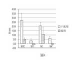
參照圖2,圖2圖示一圖解,繪示依據本技術的實施例之材料變性及低電力電漿的累加效應。如所繪示的,示例性製程可包括相對於基板表面上的碳化物薄膜移除氧化物薄膜。如由第一個棒所示,反應性離子蝕刻法或連續的波形製程可針對氧化物材料相對於碳化物材料提供低於10:1的選擇性。這可能部分地是由於由離子製程所造成的濺散,該濺散對於所有材料是更具有攻擊性的而藉此增加了兩者的蝕刻速率。並且,反應性離子蝕刻亦可能在蝕刻剖面中產生圓角,且一旦所需的薄膜已被移除,反應性離子蝕刻亦可能由於離子轟擊而蝕刻到下層的層。據此,反應性離子蝕刻對於選擇性處理及維持基板的特徵而言不是令人滿意的。Referring to FIG. 2, FIG. 2 illustrates a diagram illustrating the additive effects of material denaturation and low power plasma in accordance with embodiments of the present technology. As depicted, an exemplary process may include removing the oxide film relative to the carbide film on the substrate surface. As shown by the first bar, reactive ion etching or a continuous waveform process can provide a selectivity of less than 10:1 for oxide materials to carbide materials. This may be due in part to the sputtering caused by the ion process, which is more aggressive for all materials thereby increasing the etch rate of both. Also, reactive ion etching may also produce rounded corners in the etch profile, and may also etch the underlying layers due to ion bombardment once the desired thin film has been removed. Accordingly, reactive ion etching is not satisfactory for selectively processing and maintaining features of substrates.
如第二個棒中所示,藉由僅利用上述的脈衝式低電力RF偏壓電漿(例如同脈衝式DC電源利用),可相對於傳統的反應性離子蝕刻製程改良選擇性。該製程亦可減少或消除由反應性離子蝕刻法所產生的圓角化及下層的層的蝕刻。然而,第三個棒繪示了在執行低電力脈衝之前執行材料變性的有加成作用的益處。藉由利用兩種薄膜變性以及低電力電漿RF脈衝製程,選擇性相對於反應性離子蝕刻製程增加了幾乎一個數量級。此外,在減少圓角化及下層的層的蝕刻的情況下,蝕刻剖面被更加改良了。As shown in the second bar, by utilizing only the pulsed low power RF bias plasma described above (eg, with a pulsed DC power supply), selectivity can be improved over conventional reactive ion etching processes. The process also reduces or eliminates the filleting and etching of underlying layers caused by reactive ion etching. However, the third bar depicts the additive benefit of performing material denaturation prior to performing the low power pulse. By utilizing both thin film denaturation and low power plasma RF pulse processes, selectivity is increased by almost an order of magnitude relative to reactive ion etching processes. In addition, the etching profile is further improved while reducing rounding and etching of underlying layers.
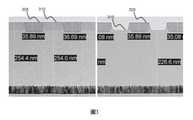
圖3繪示依據本技術的實施例來執行之蝕刻製程的成像。如左方影像中所示,氮化矽區域305安置在碳化矽區域310之間。在執行如先前所討論的材料變性及低電力RF蝕刻操作之後,碳化矽區段被移除了,如右方圖式中所繪示。實質上維持了氮化矽層305,且僅可觀察到最小限度的圓角化。此外,在碳化矽區段310下層的氧化矽層315在蝕刻製程期間受暴,但該薄膜能夠充當製程的蝕刻停止物,與由於氧化矽的轟擊而會蝕刻進溝的反應性離子製程相反。量測到的效果說明的是,本技術能夠在最小限度地圓角化氮化矽的情況下產生超過50:1的碳化矽對氮化矽的蝕刻選擇性。本技術亦能夠產生超過70:1的碳化矽對氧化矽的蝕刻選擇性。3 illustrates imaging of an etch process performed in accordance with embodiments of the present technology. As shown in the left image,
圖4圖示一圖表,繪示在使用及不使用依據本技術的實施例的處理的情況下的各種材料的蝕刻速率。本實例圖示了在電漿中利用氧母材來使基板表面上受暴的碳氧化矽、氧化矽、碳化矽及氮化矽變性的材料變性。在使用及不使用該氧處理的情況下在類似的材料上執行低電力脈衝式RF蝕刻製程。如所繪示,是在不使用材料變性的情況下在低電力蝕刻製程期間以低選擇性蝕刻所有四個薄膜。另一方面來說,在氧處理之後,碳氧化矽及碳化矽持續蝕刻,同時氧化矽及氮化矽薄膜被向那些薄膜提供表面強化的氧處理實質維持住及緩衝了。4 illustrates a graph showing etch rates for various materials with and without processing in accordance with embodiments of the present technology. This example illustrates the use of an oxygen base material in a plasma to denature exposed silicon oxycarbide, silicon oxide, silicon carbide, and silicon nitride denatured materials on a substrate surface. Low power pulsed RF etch processes were performed on similar materials with and without the oxygen treatment. As shown, all four films are etched with low selectivity during the low power etch process without the use of material denaturation. On the other hand, after the oxygen treatment, the silicon oxycarbide and silicon carbide continue to etch, while the silicon oxide and silicon nitride films are substantially maintained and buffered by the oxygen treatment that provides surface enhancement to those films.
圖5圖示一圖表,繪示在使用及不使用依據本技術的實施例的處理的情況下的碳氧化矽及碳化矽的蝕刻速率。雖然在圖4中所繪示之實例中所執行的氧變性相對於氧化矽及氮化矽而言對於含碳的薄膜是成功的,兩個含碳的薄膜相對於彼此並不具高的選擇性。在圖5中,執行了利用碳氧化矽薄膜的較高多孔性的物理變性。碳氧化矽相較於碳化矽而言是更加多孔的薄膜,且化學鍵結亦是較弱的。此示例的物理變性包括了在電漿中利用氦母材,且接著將薄膜暴露於那些電漿溢流。雖然氦離子的衝擊具有充足的損傷碳氧化矽之化學鍵的能力,但因為氦對於兩個薄膜而言是惰性的,其在化學上並不與材料反應。這進一步弱化了薄膜,在這之後執行低電力RF脈衝蝕刻。如由圖式所繪示,在變性之後進行低電力蝕刻移除了碳氧化矽材料同時實質上維持了碳化矽。5 illustrates a graph showing etch rates of silicon oxycarbide and silicon carbide with and without processing in accordance with embodiments of the present technology. Although the oxygen denaturation performed in the example depicted in Figure 4 was successful for carbon-containing films relative to silicon oxide and silicon nitride, the two carbon-containing films were not highly selective with respect to each other . In Figure 5, physical denaturation utilizing the higher porosity of silicon oxycarbide films was performed. Silicon oxycarbide is a more porous film than silicon carbide, and the chemical bonds are weaker. Physical modifications of this example included utilizing a helium parent material in a plasma, and then exposing the film to those plasma floods. Although the impact of helium ions has sufficient capacity to damage the chemical bonds of the silicon oxycarbide, because helium is inert to the two films, it does not chemically react with the material. This further weakens the film, after which a low power RF pulse etch is performed. As shown by the figures, a low power etch after denaturation removes the silicon oxycarbide material while substantially maintaining the silicon carbide.
由圖4及5所繪示的實例僅為示例性的,且不是要限制本技術。這些實例僅顯示由本技術所包括之材料變性的類型。具技藝者將藉由這些實例輕易瞭解可如何將材料變性及低電力蝕刻操作應用於各種材料來強化選擇性且改良蝕刻剖面。藉由利用本技術,可針對碳氧化矽相對於氧化矽及氮化矽達成大於20:1的選擇性。亦可使用依據本技術的各種材料變性及蝕刻來針對氧化矽相對於碳氧化矽、氮化矽及碳化矽達成大於20:1的選擇性。亦可使用依據本技術的各種材料變性及蝕刻來針對碳化矽相對於氧化矽、氮化矽及碳氧化矽達成大於20:1的選擇性。此外,可使用依據本技術的各種材料變性及蝕刻來針對氮化矽相對於氧化矽、碳氧化矽及碳化矽達成大於20:1的選擇性。在實施例中,任何這些操作的選擇性亦可大於或約為25:1、大於或約為30:1、大於或約為35:1 、大於或約為40:1、大於或約為45:1、大於或約為50:1、大於或約為55:1、大於或約為60:1、大於或約為65:1、大於或約為70:1、大於或約為75:1、大於或約為80:1、大於或約為85:1、大於或約為90:1、大於或約為95:1、或大於或約為100:1。The examples depicted by Figures 4 and 5 are exemplary only, and are not intended to limit the present technology. These examples only show the types of material modifications encompassed by the present technology. Those skilled in the art will readily understand from these examples how material denaturation and low power etch operations can be applied to various materials to enhance selectivity and improve etch profiles. By utilizing this technique, a selectivity of greater than 20:1 for silicon oxycarbide relative to silicon oxide and silicon nitride can be achieved. Various material modifications and etchings in accordance with the present techniques can also be used to achieve greater than 20:1 selectivities for silicon oxide over silicon oxycarbide, silicon nitride, and silicon carbide. Various material modifications and etchings in accordance with the present techniques can also be used to achieve greater than 20:1 selectivities for silicon carbide over silicon oxide, silicon nitride, and silicon oxycarbide. In addition, various material modifications and etchings in accordance with the present techniques can be used to achieve greater than 20:1 selectivities for silicon nitride over silicon oxide, silicon oxycarbide, and silicon carbide. In embodiments, the selectivity of any of these operations may also be greater than or about 25:1, greater than or about 30:1, greater than or about 35:1, greater than or about 40:1, greater than or about 45 :1, greater than or approximately 50:1, greater than or approximately 55:1, greater than or approximately 60:1, greater than or approximately 65:1, greater than or approximately 70:1, greater than or approximately 75:1 , greater than or about 80:1, greater than or about 85:1, greater than or about 90:1, greater than or about 95:1, or greater than or about 100:1.
參照圖6,圖6圖示依據本技術的實施例之向靜電夾具提供DC脈衝之控制器的部分示意說明。該系統可被包括為具有依據本技術的實施例的基板處理腔室。示例性腔室可為由加州聖克拉拉市的應用材料公司所生產的MesaTM蝕刻系統。元件可包括被配置為支撐半導體基板的托架605。該系統亦可包括與托架電耦合且被配置為如先前所述地產生電漿的脈衝式RF偏壓電源610。脈衝式RF偏壓電源610可被配置為以約20 W及約50 W之間的功率在處理腔室內產生電漿,且脈衝式RF偏壓電源可在低於約5,000 Hz的頻率下發出脈衝。該系統亦可被配置為在先前所述的任何其他的位準下運作。Referring to FIG. 6, FIG. 6 illustrates a partial schematic illustration of a controller that provides DC pulses to an electrostatic clamp in accordance with an embodiment of the present technology. The system may be included as having a substrate processing chamber in accordance with embodiments of the present technology. An exemplary chamber may be the Mesa™ etch system produced by Applied Materials, Inc. of Santa Clara, California. The element may include a
該系統亦可包括與基板處理腔室電耦合的DC脈衝電源615。DC脈衝電源615可如先前所述的,且被配置為針對RF偏壓電漿產生引火粒子。在實施例中,DC脈衝電源可被配置為以一定頻率發出脈衝以在不發展電漿鞘的情況下產生引火粒子。DC脈衝電源可以先前所述的任何時間點或在先前所述的任何工作週期下運作,且可被配置為在小於約50%的工作週期下以100微秒或更少的持續時間發出脈衝。DC脈衝電源亦可被配置為在小於約20%的工作週期下以小於約50微秒的脈衝持續期間運作。在實施例中,DC脈衝電源亦可被配置為在小於約10%的工作週期下以小於約10微秒的脈衝持續期間運作。The system may also include a DC
如圖6中所繪示,托架605可為靜電夾具。腔室控制器620可向靜電夾具控制器625(包括用於雙極靜電夾具的輸入/輸出模組630)提供指令。DC脈衝電源615可如圖式中所繪示地與雙極靜電夾具630的電接地電耦合。在許多處理腔室中,電極可被偏壓至DC電壓,且可在DC電源供應器的輸出處包括重濾波(heavy filtering)以阻擋RF電力。從而,在電源如配置中所示地發出脈衝時,波形可開始扭曲及衰減。據此,為了克服此問題,靜電夾具電源可在脈衝式DC的電壓處浮動。因此,靜電夾具電極接著參考了脈衝式DC的高電壓。換言之,靜電夾具電源可接著浮動而在電學上與機器的接地隔離,且靜電夾具的接地實質上可在高電壓處。靜電夾具可接著相對於高電壓輸出正及負極性。As shown in FIG. 6, the
因此,若脈衝式DC關閉循環或接地,則靜電夾具電極會以正或負的方式參考接地。然而,在DC被施用或發出脈衝時,則靜電夾具電極會參考所施用之DC電源的電源。為瞭解釋的目的而非作為特定的製程情境,作為如此配置的非限制性實例,若脈衝式DC電源在1 kV下運作,且靜電夾具在+/- 500伏特下運作,則在DC電源啟動循環以如先前所述地協助電漿生成時,電極會分別處於1500伏特及500伏特。此配置的益處可為,在腔室裡面可能不需要用於脈衝式DC電源的額外導體。此外,在實施例中,DC及RF脈衝可為交替的,且因此DC及RF電源儘管它們各偏壓相同的托架基座亦可彼此解耦。Therefore, if the pulsed DC is cycled off or grounded, the electrostatic clamp electrodes are either positively or negatively referenced to ground. However, when DC is applied or pulsed, then the electrostatic clamp electrodes are referenced to the power of the applied DC power source. For purposes of explanation and not as a specific process context, as a non-limiting example of such a configuration, if the pulsed DC power supply operates at 1 kV and the electrostatic clamp operates at +/- 500 volts, then the DC power supply starts The electrodes were at 1500 volts and 500 volts, respectively, when cycling to assist plasma generation as previously described. The benefit of this configuration may be that additional conductors for the pulsed DC power supply may not be required inside the chamber. Furthermore, in an embodiment, the DC and RF pulses may be alternated, and thus the DC and RF power supplies may be decoupled from each other despite their respective biased cradle bases.
可與靜電夾具解耦的額外耦合選項繪示於圖7中,圖7圖示依據本技術的實施例之向與托架結構耦合之導體提供DC脈衝之控制器的部分示意說明。如圖式中所繪示,基板處理腔室701被圖示為具有蓮蓬頭703及被配置為支撐基板的托架705。該系統可包括如先前所討論的脈衝式RF徧壓710,以及用於靜電夾持的DC電源715。可包括額外的DC脈衝單元720,該單元提供如先前所討論的脈衝式DC電源以供產生引火以供由RF偏壓點燃電漿。在此實例中,DC脈衝電源與導電環725電耦合,該導電環嵌在托架中或與該托架耦合。此導電環725在實施例中可與靜電夾具解耦及與RF偏壓解耦。例如,導電環725可被包括在托架705的介電罩環(包括石英罩環)中,如圖示。在實施例中,導電環可為任何導電材料,包括金屬或碳化矽。在此情境中,雖然因為導電環與其他電源解耦而在系統中包括了額外的導體,該等元件並不需要相對於彼此在電學上浮動。Additional coupling options that can be decoupled from the electrostatic clamp are depicted in FIG. 7, which illustrates a partial schematic illustration of a controller that provides DC pulses to conductors coupled to the carrier structure in accordance with an embodiment of the present technology. As depicted in the figures, a
可與靜電夾具解耦的另一耦合選項繪示於圖8中,圖8圖示依據本技術的實施例之向處理腔室之蓮蓬頭內的嵌式導體提供DC脈衝之控制器的部分示意說明。如所繪示的,圖示了與針對圖7所討論的那些元件類似的元件,包括基板處理腔室701,該基板處理腔室包括蓮蓬頭703及托架705,舉例而言。該系統類似地包括脈衝式RF徧壓710、用於靜電夾持的DC電源715及DC脈衝單元720。圖式額外包括了導電環825,該導電環可為上文所討論的類似材料,但在實施例中可與蓮蓬頭703耦合。此耦合選項亦將脈衝式DC與其他電源解耦。Another coupling option that can be decoupled from the electrostatic clamp is shown in FIG. 8, which shows a partial schematic illustration of a controller that provides DC pulses to embedded conductors in a showerhead of a processing chamber in accordance with an embodiment of the present technology . As depicted, elements similar to those discussed with respect to FIG. 7 are illustrated, including a
亦可在實施例中包括與腔室壁耦合或嵌在該腔室壁中的耦合環,或與腔室系統的其他元件耦合或嵌在該等其他元件中的耦合環。藉由以任何這些選項或如會輕易地瞭解到要類似地包括的替代選項提供脈衝式DC電源,該系統相較於傳統系統可產生較低電力的電漿。藉由提供能量來產生高能粒子而允許低電力的脈衝RF偏壓更容易以較低的離子能量在較低的電壓下使電漿放電,可針對蝕刻、沉積、清潔或可受益於低電力電漿的任何其他製程提供改良的電漿處理。Embodiments may also include coupling loops coupled to or embedded in the walls of the chamber, or coupling loops coupled to or embedded in other elements of the chamber system. By providing pulsed DC power in any of these options, or alternative options as would be readily understood to be similarly included, the system can generate a lower power plasma than conventional systems. Pulsed RF bias that allows low power by providing energy to generate high-energy particles makes it easier to discharge plasma at lower voltages with lower ion energy, can be targeted for etching, deposition, cleaning or can benefit from low-power electrical Any other process of slurry provides improved plasma treatment.
在上述說明中,為了解釋的目的,已闡述了許多細節以提供本技術之各種實施例的瞭解。然而,本領域中具技藝者將理解的是,可在沒有某些這些細節的情況下或在有額外的細節的情況下實行某些實施例。In the foregoing description, for the purposes of explanation, numerous details have been set forth in order to provide an understanding of various embodiments of the present technology. However, it will be understood by those skilled in the art that certain embodiments may be practiced without some of these details or with additional details.
在已揭露了若干實施例的情況下,將由本領域中具技藝者所辨識的是,可在不脫離實施例之精神的情況下使用各種變體、替代構造及等效物。此外,未描述許多習知的製程及構件以避免不必要地模糊了本技術。據此,不應將以上說明視為限制了本技術的範圍。Having disclosed several embodiments, it will be recognized by those skilled in the art that various modifications, alternative constructions, and equivalents may be used without departing from the spirit of the embodiments. Furthermore, many well-known processes and components have not been described in order to avoid unnecessarily obscuring the present technology. Accordingly, the above description should not be construed as limiting the scope of the present technology.
若提供了值的範圍,則瞭解的是,亦具體揭露了該範圍之上限及下限之間的各個中介值(揭露到下限的最小的單位小數),除非上下文另有清楚指定。包括了任何經陳述的值之間的任何較窄範圍或經陳述範圍中的未經陳述的中介值及該經陳述範圍中的任何其他經陳述的或中介的值。可獨立地在範圍中包括或排除那些較小範圍的上限及下限,且在較小範圍中包括任一限值、不包括任何限值或包括兩個限值的各個範圍亦被包括在本技術內,取決於經陳述範圍中的任何被具體排除的限值。若經陳述的範圍包括該等限值中的一者或兩者,則亦包括了排除該等經包括之限值中之任一者或兩者的範圍。若在列表中提供了多個值,則類似地具體揭露了包括任何這些值或基於任何這些值的任何範圍。If a range of values is provided, it is understood that each intervening value (to the smallest single decimal of the lower limit) between the upper and lower limits of the range is also specifically disclosed, unless the context clearly dictates otherwise. Any narrower range between any stated value or unrecited intervening value in a stated range and any other stated or intervening value in that stated range is included. The upper and lower limits of those smaller ranges may independently be included or excluded in the range, and each range including either limit, excluding either limit, or both limits in the smaller ranges is also encompassed within the present technology within the stated range, subject to any specifically excluded limit in the stated range. Where the stated range includes one or both of the limits, ranges excluding either or both of the included limits are also included. If multiple values are provided in a list, any ranges including or based on any of these values are similarly specifically disclosed.
如本文中及隨附請求項中所使用的,單數形式「一(a)」、「一「an」」及「該」包括了複數的指稱,除非上下文另有清楚指定。例如,因此,對於「一種材料」的指稱包括了複數種此類材料,且對於「該母材」的指稱包括了對於本領域中具技藝者所習知的一或更多種母材及其等效物的指稱等等。As used herein and in the appended claims, the singular forms "a (a)," "an," and "the" include plural referents unless the context clearly dictates otherwise. Thus, for example, reference to "a material" includes a plurality of such materials, and reference to "the parent material" includes reference to one or more parent materials and the like known to those skilled in the art. References to equivalents, etc.
並且,用字「包括(comprise)」、「包括(comprising)」、「包含(contain)」、「包含(containing)」、「包括(include)」及「包括(including)」在被用在此說明書中及以下請求項中時,是要指定經陳述的特徵、整數、元件或操作的存在,但該等用字並不排除一或更多個其他的特徵、整數、元件、操作、行動或群組的存在或添加。Also, the words "comprise", "comprising", "contain", "containing", "include" and "including" are used herein In the specification and in the following claims, the presence of a stated feature, integer, element or operation is intended to be specified, but such wording does not exclude one or more other features, integers, elements, operations, actions or The existence or addition of a group.
100‧‧‧方法110-130‧‧‧操作305‧‧‧氮化矽區域310‧‧‧碳化矽區域315‧‧‧氧化矽層605‧‧‧托架610‧‧‧RF偏壓電源615‧‧‧DC脈衝電源620‧‧‧腔室控制器625‧‧‧靜電夾具控制器630‧‧‧雙極靜電夾具701‧‧‧腔室703‧‧‧蓮蓬頭705‧‧‧托架710‧‧‧RF偏壓715‧‧‧DC電源720‧‧‧DC脈衝單元725‧‧‧導電環825‧‧‧導電環100‧‧‧Methods 110-130‧‧‧
可藉由參照本說明書的其餘部分及繪圖來實現所揭露之實施例之本質及優點的進一步瞭解。A further understanding of the nature and advantages of the disclosed embodiments can be realized by reference to the remainder of the specification and the drawings.
圖1繪示依據本技術的實施例來蝕刻基板的方法。1 illustrates a method of etching a substrate in accordance with an embodiment of the present technology.
圖2圖示一圖解,繪示依據本技術的實施例之材料變性及低電力電漿的累加效應。2 illustrates a diagram illustrating the additive effects of material denaturation and low power plasma in accordance with embodiments of the present technology.
圖3圖示依據本技術的實施例來執行之蝕刻製程的成像。3 illustrates imaging of an etch process performed in accordance with embodiments of the present technology.
圖4圖示一圖表,繪示在使用及不使用依據本技術的實施例的處理的情況下的各種材料的蝕刻速率。4 illustrates a graph showing etch rates for various materials with and without processing in accordance with embodiments of the present technology.
圖5圖示一圖表,繪示在使用及不使用依據本技術的實施例的處理的情況下的碳氧化矽及碳化矽的蝕刻速率。5 illustrates a graph showing etch rates of silicon oxycarbide and silicon carbide with and without processing in accordance with embodiments of the present technology.
圖6圖示依據本技術的實施例之向靜電夾具提供DC脈衝之控制器的部分示意說明。6 illustrates a partial schematic illustration of a controller that provides DC pulses to an electrostatic clamp in accordance with an embodiment of the present technology.
圖7圖示依據本技術的實施例之向導體提供DC脈衝之控制器的部分示意說明,該導體與處理腔室內的托架結構耦合。7 illustrates a partial schematic illustration of a controller that provides DC pulses to conductors coupled to carriage structures within a processing chamber in accordance with an embodiment of the present technology.
圖8圖示依據本技術的實施例之向導體提供DC脈衝之控制器的部分示意說明,該導體與處理腔室的蓮蓬頭耦合。8 shows a partial schematic illustration of a controller that provides DC pulses to conductors coupled to a showerhead of a processing chamber in accordance with an embodiment of the present technology.
在隨附的圖式中,類似的元件及/或特徵可具有相同的數字參考標示。進一步地,可藉由在參考標示之後加上一字母來區隔相同類型的各種元件,該字母在類似的元件及/或特徵之中進行區隔。若在本說明書中僅使用第一數字參考標示,則該說明適用於具有相同第一數字參考標示之類似元件及/或特徵中的任何一者而不論字母字尾。In the accompanying drawings, similar elements and/or features may have the same numerical references. Further, various elements of the same type may be distinguished by following the reference designation by a letter that distinguishes among similar elements and/or features. If only a first numerical reference is used in this specification, the description applies to any of the similar elements and/or features having the same first numerical reference regardless of the letter suffix.
國內寄存資訊 (請依寄存機構、日期、號碼順序註記) 無Domestic storage information (please note in the order of storage institution, date and number) None
國外寄存資訊 (請依寄存國家、機構、日期、號碼順序註記) 無Foreign deposit information (please note in the order of deposit country, institution, date and number) None
605‧‧‧托架605‧‧‧Bracket
610‧‧‧RF偏壓電源610‧‧‧RF Bias Power Supply
615‧‧‧DC脈衝電源615‧‧‧DC pulse power supply
620‧‧‧腔室控制器620‧‧‧Chamber Controller
625‧‧‧靜電夾具控制器625‧‧‧Electrostatic Fixture Controller
630‧‧‧雙極靜電夾具630‧‧‧Bipolar electrostatic clamp
Claims (20)
Translated fromChineseApplications Claiming Priority (2)
| Application Number | Priority Date | Filing Date | Title |
|---|---|---|---|
| US15/197,060 | 2016-06-29 | ||
| US15/197,060US9865484B1 (en) | 2016-06-29 | 2016-06-29 | Selective etch using material modification and RF pulsing |
Publications (2)
| Publication Number | Publication Date |
|---|---|
| TW201810422A TW201810422A (en) | 2018-03-16 |
| TWI756234Btrue TWI756234B (en) | 2022-03-01 |
Family
ID=60785206
Family Applications (1)
| Application Number | Title | Priority Date | Filing Date |
|---|---|---|---|
| TW106121039ATWI756234B (en) | 2016-06-29 | 2017-06-23 | Selective etch using material modification and rf pulsing |
Country Status (6)
| Country | Link |
|---|---|
| US (2) | US9865484B1 (en) |
| JP (1) | JP6719602B2 (en) |
| KR (1) | KR102167957B1 (en) |
| CN (1) | CN109417028B (en) |
| TW (1) | TWI756234B (en) |
| WO (1) | WO2018005122A1 (en) |
Families Citing this family (97)
| Publication number | Priority date | Publication date | Assignee | Title |
|---|---|---|---|---|
| US10283321B2 (en) | 2011-01-18 | 2019-05-07 | Applied Materials, Inc. | Semiconductor processing system and methods using capacitively coupled plasma |
| US9373517B2 (en) | 2012-08-02 | 2016-06-21 | Applied Materials, Inc. | Semiconductor processing with DC assisted RF power for improved control |
| US9132436B2 (en) | 2012-09-21 | 2015-09-15 | Applied Materials, Inc. | Chemical control features in wafer process equipment |
| US10256079B2 (en) | 2013-02-08 | 2019-04-09 | Applied Materials, Inc. | Semiconductor processing systems having multiple plasma configurations |
| US9362130B2 (en) | 2013-03-01 | 2016-06-07 | Applied Materials, Inc. | Enhanced etching processes using remote plasma sources |
| US9309598B2 (en) | 2014-05-28 | 2016-04-12 | Applied Materials, Inc. | Oxide and metal removal |
| US9355922B2 (en) | 2014-10-14 | 2016-05-31 | Applied Materials, Inc. | Systems and methods for internal surface conditioning in plasma processing equipment |
| US9966240B2 (en) | 2014-10-14 | 2018-05-08 | Applied Materials, Inc. | Systems and methods for internal surface conditioning assessment in plasma processing equipment |
| US11637002B2 (en) | 2014-11-26 | 2023-04-25 | Applied Materials, Inc. | Methods and systems to enhance process uniformity |
| US10573496B2 (en) | 2014-12-09 | 2020-02-25 | Applied Materials, Inc. | Direct outlet toroidal plasma source |
| US10224210B2 (en) | 2014-12-09 | 2019-03-05 | Applied Materials, Inc. | Plasma processing system with direct outlet toroidal plasma source |
| US11257693B2 (en) | 2015-01-09 | 2022-02-22 | Applied Materials, Inc. | Methods and systems to improve pedestal temperature control |
| US9728437B2 (en) | 2015-02-03 | 2017-08-08 | Applied Materials, Inc. | High temperature chuck for plasma processing systems |
| US20160225652A1 (en) | 2015-02-03 | 2016-08-04 | Applied Materials, Inc. | Low temperature chuck for plasma processing systems |
| US9691645B2 (en) | 2015-08-06 | 2017-06-27 | Applied Materials, Inc. | Bolted wafer chuck thermal management systems and methods for wafer processing systems |
| US9741593B2 (en) | 2015-08-06 | 2017-08-22 | Applied Materials, Inc. | Thermal management systems and methods for wafer processing systems |
| US9349605B1 (en) | 2015-08-07 | 2016-05-24 | Applied Materials, Inc. | Oxide etch selectivity systems and methods |
| US10504700B2 (en) | 2015-08-27 | 2019-12-10 | Applied Materials, Inc. | Plasma etching systems and methods with secondary plasma injection |
| US10504754B2 (en) | 2016-05-19 | 2019-12-10 | Applied Materials, Inc. | Systems and methods for improved semiconductor etching and component protection |
| US10522371B2 (en) | 2016-05-19 | 2019-12-31 | Applied Materials, Inc. | Systems and methods for improved semiconductor etching and component protection |
| US9865484B1 (en) | 2016-06-29 | 2018-01-09 | Applied Materials, Inc. | Selective etch using material modification and RF pulsing |
| US10629473B2 (en) | 2016-09-09 | 2020-04-21 | Applied Materials, Inc. | Footing removal for nitride spacer |
| US10062575B2 (en) | 2016-09-09 | 2018-08-28 | Applied Materials, Inc. | Poly directional etch by oxidation |
| US10062585B2 (en) | 2016-10-04 | 2018-08-28 | Applied Materials, Inc. | Oxygen compatible plasma source |
| US9934942B1 (en) | 2016-10-04 | 2018-04-03 | Applied Materials, Inc. | Chamber with flow-through source |
| US10546729B2 (en) | 2016-10-04 | 2020-01-28 | Applied Materials, Inc. | Dual-channel showerhead with improved profile |
| US10062579B2 (en) | 2016-10-07 | 2018-08-28 | Applied Materials, Inc. | Selective SiN lateral recess |
| US9768034B1 (en) | 2016-11-11 | 2017-09-19 | Applied Materials, Inc. | Removal methods for high aspect ratio structures |
| US10163696B2 (en) | 2016-11-11 | 2018-12-25 | Applied Materials, Inc. | Selective cobalt removal for bottom up gapfill |
| US10026621B2 (en) | 2016-11-14 | 2018-07-17 | Applied Materials, Inc. | SiN spacer profile patterning |
| US10242908B2 (en) | 2016-11-14 | 2019-03-26 | Applied Materials, Inc. | Airgap formation with damage-free copper |
| US10566212B2 (en) | 2016-12-19 | 2020-02-18 | Lam Research Corporation | Designer atomic layer etching |
| US10566206B2 (en) | 2016-12-27 | 2020-02-18 | Applied Materials, Inc. | Systems and methods for anisotropic material breakthrough |
| US10403507B2 (en) | 2017-02-03 | 2019-09-03 | Applied Materials, Inc. | Shaped etch profile with oxidation |
| US10431429B2 (en) | 2017-02-03 | 2019-10-01 | Applied Materials, Inc. | Systems and methods for radial and azimuthal control of plasma uniformity |
| US10043684B1 (en) | 2017-02-06 | 2018-08-07 | Applied Materials, Inc. | Self-limiting atomic thermal etching systems and methods |
| US10319739B2 (en) | 2017-02-08 | 2019-06-11 | Applied Materials, Inc. | Accommodating imperfectly aligned memory holes |
| US10943834B2 (en) | 2017-03-13 | 2021-03-09 | Applied Materials, Inc. | Replacement contact process |
| US10319649B2 (en) | 2017-04-11 | 2019-06-11 | Applied Materials, Inc. | Optical emission spectroscopy (OES) for remote plasma monitoring |
| US11276590B2 (en) | 2017-05-17 | 2022-03-15 | Applied Materials, Inc. | Multi-zone semiconductor substrate supports |
| JP7176860B6 (en) | 2017-05-17 | 2022-12-16 | アプライド マテリアルズ インコーポレイテッド | Semiconductor processing chamber to improve precursor flow |
| US11276559B2 (en) | 2017-05-17 | 2022-03-15 | Applied Materials, Inc. | Semiconductor processing chamber for multiple precursor flow |
| US10049891B1 (en) | 2017-05-31 | 2018-08-14 | Applied Materials, Inc. | Selective in situ cobalt residue removal |
| US10497579B2 (en) | 2017-05-31 | 2019-12-03 | Applied Materials, Inc. | Water-free etching methods |
| US10920320B2 (en) | 2017-06-16 | 2021-02-16 | Applied Materials, Inc. | Plasma health determination in semiconductor substrate processing reactors |
| US10541246B2 (en) | 2017-06-26 | 2020-01-21 | Applied Materials, Inc. | 3D flash memory cells which discourage cross-cell electrical tunneling |
| US10727080B2 (en) | 2017-07-07 | 2020-07-28 | Applied Materials, Inc. | Tantalum-containing material removal |
| US10541184B2 (en) | 2017-07-11 | 2020-01-21 | Applied Materials, Inc. | Optical emission spectroscopic techniques for monitoring etching |
| US10354889B2 (en) | 2017-07-17 | 2019-07-16 | Applied Materials, Inc. | Non-halogen etching of silicon-containing materials |
| US10043674B1 (en) | 2017-08-04 | 2018-08-07 | Applied Materials, Inc. | Germanium etching systems and methods |
| US10170336B1 (en) | 2017-08-04 | 2019-01-01 | Applied Materials, Inc. | Methods for anisotropic control of selective silicon removal |
| US10297458B2 (en) | 2017-08-07 | 2019-05-21 | Applied Materials, Inc. | Process window widening using coated parts in plasma etch processes |
| US10636675B2 (en) | 2017-09-27 | 2020-04-28 | Applied Materials, Inc. | Methods of etching metal-containing layers |
| US10763083B2 (en)* | 2017-10-06 | 2020-09-01 | Lam Research Corporation | High energy atomic layer etching |
| US10424487B2 (en) | 2017-10-24 | 2019-09-24 | Applied Materials, Inc. | Atomic layer etching processes |
| US10283324B1 (en) | 2017-10-24 | 2019-05-07 | Applied Materials, Inc. | Oxygen treatment for nitride etching |
| US10128086B1 (en) | 2017-10-24 | 2018-11-13 | Applied Materials, Inc. | Silicon pretreatment for nitride removal |
| JP6877316B2 (en)* | 2017-11-08 | 2021-05-26 | 東京エレクトロン株式会社 | Etching method |
| US10741392B2 (en)* | 2017-11-28 | 2020-08-11 | Taiwan Semiconductor Manufacturing Co., Ltd. | Method for forming semiconductor structure |
| US10256112B1 (en) | 2017-12-08 | 2019-04-09 | Applied Materials, Inc. | Selective tungsten removal |
| US10903054B2 (en) | 2017-12-19 | 2021-01-26 | Applied Materials, Inc. | Multi-zone gas distribution systems and methods |
| US11328909B2 (en) | 2017-12-22 | 2022-05-10 | Applied Materials, Inc. | Chamber conditioning and removal processes |
| US10854426B2 (en) | 2018-01-08 | 2020-12-01 | Applied Materials, Inc. | Metal recess for semiconductor structures |
| US10964512B2 (en) | 2018-02-15 | 2021-03-30 | Applied Materials, Inc. | Semiconductor processing chamber multistage mixing apparatus and methods |
| US10679870B2 (en) | 2018-02-15 | 2020-06-09 | Applied Materials, Inc. | Semiconductor processing chamber multistage mixing apparatus |
| JP7025952B2 (en)* | 2018-02-16 | 2022-02-25 | 東京エレクトロン株式会社 | Etching method and plasma processing equipment |
| TWI766433B (en) | 2018-02-28 | 2022-06-01 | 美商應用材料股份有限公司 | Systems and methods to form airgaps |
| US10593560B2 (en) | 2018-03-01 | 2020-03-17 | Applied Materials, Inc. | Magnetic induction plasma source for semiconductor processes and equipment |
| US10319600B1 (en) | 2018-03-12 | 2019-06-11 | Applied Materials, Inc. | Thermal silicon etch |
| US10497573B2 (en) | 2018-03-13 | 2019-12-03 | Applied Materials, Inc. | Selective atomic layer etching of semiconductor materials |
| US11450513B2 (en)* | 2018-03-30 | 2022-09-20 | Lam Research Corporation | Atomic layer etching and smoothing of refractory metals and other high surface binding energy materials |
| US10573527B2 (en) | 2018-04-06 | 2020-02-25 | Applied Materials, Inc. | Gas-phase selective etching systems and methods |
| US10490406B2 (en) | 2018-04-10 | 2019-11-26 | Appled Materials, Inc. | Systems and methods for material breakthrough |
| US10699879B2 (en) | 2018-04-17 | 2020-06-30 | Applied Materials, Inc. | Two piece electrode assembly with gap for plasma control |
| US10886137B2 (en) | 2018-04-30 | 2021-01-05 | Applied Materials, Inc. | Selective nitride removal |
| US10555412B2 (en)* | 2018-05-10 | 2020-02-04 | Applied Materials, Inc. | Method of controlling ion energy distribution using a pulse generator with a current-return output stage |
| US10872778B2 (en) | 2018-07-06 | 2020-12-22 | Applied Materials, Inc. | Systems and methods utilizing solid-phase etchants |
| US10755941B2 (en) | 2018-07-06 | 2020-08-25 | Applied Materials, Inc. | Self-limiting selective etching systems and methods |
| US10672642B2 (en) | 2018-07-24 | 2020-06-02 | Applied Materials, Inc. | Systems and methods for pedestal configuration |
| US10892198B2 (en) | 2018-09-14 | 2021-01-12 | Applied Materials, Inc. | Systems and methods for improved performance in semiconductor processing |
| US11049755B2 (en) | 2018-09-14 | 2021-06-29 | Applied Materials, Inc. | Semiconductor substrate supports with embedded RF shield |
| US11062887B2 (en) | 2018-09-17 | 2021-07-13 | Applied Materials, Inc. | High temperature RF heater pedestals |
| US11114306B2 (en) | 2018-09-17 | 2021-09-07 | Applied Materials, Inc. | Methods for depositing dielectric material |
| US11417534B2 (en) | 2018-09-21 | 2022-08-16 | Applied Materials, Inc. | Selective material removal |
| US10971357B2 (en) | 2018-10-04 | 2021-04-06 | Applied Materials, Inc. | Thin film treatment process |
| US11682560B2 (en) | 2018-10-11 | 2023-06-20 | Applied Materials, Inc. | Systems and methods for hafnium-containing film removal |
| US11121002B2 (en) | 2018-10-24 | 2021-09-14 | Applied Materials, Inc. | Systems and methods for etching metals and metal derivatives |
| US11437242B2 (en) | 2018-11-27 | 2022-09-06 | Applied Materials, Inc. | Selective removal of silicon-containing materials |
| US11721527B2 (en) | 2019-01-07 | 2023-08-08 | Applied Materials, Inc. | Processing chamber mixing systems |
| US10920319B2 (en) | 2019-01-11 | 2021-02-16 | Applied Materials, Inc. | Ceramic showerheads with conductive electrodes |
| WO2020008703A1 (en)* | 2019-04-19 | 2020-01-09 | 株式会社日立ハイテクノロジーズ | Plasma processing method |
| CN112509899B (en)* | 2019-09-16 | 2024-02-09 | 中微半导体设备(上海)股份有限公司 | Inductively coupled plasma processing apparatus and ignition control method thereof |
| CN116569311A (en)* | 2020-07-19 | 2023-08-08 | 应用材料公司 | Integrated process using boron doped silicon material |
| CN112216702B (en)* | 2020-10-09 | 2022-03-29 | 长江存储科技有限责任公司 | Etching process and 3D NAND manufacturing process |
| GB202020822D0 (en)* | 2020-12-31 | 2021-02-17 | Spts Technologies Ltd | Method and apparatus |
| US12322573B2 (en)* | 2021-05-12 | 2025-06-03 | Applied Materials, Inc. | Pulsing plasma treatment for film densification |
| CN118280819A (en)* | 2022-12-30 | 2024-07-02 | 江苏鲁汶仪器股份有限公司 | Etching method and etching system |
Citations (7)
| Publication number | Priority date | Publication date | Assignee | Title |
|---|---|---|---|---|
| US20110139748A1 (en)* | 2009-12-15 | 2011-06-16 | University Of Houston | Atomic layer etching with pulsed plasmas |
| US20120217221A1 (en)* | 2010-04-26 | 2012-08-30 | Advanced Energy Industries, Inc. | System, method and apparatus for controlling ion energy distribution of a projected plasma |
| US20150011088A1 (en)* | 2012-02-29 | 2015-01-08 | Oxford Instruments Nanotechnology Tools Limited | Methods and apparatus for depositing and/or etching material on a substrate |
| TWI539485B (en)* | 2013-03-15 | 2016-06-21 | 東京威力科創股份有限公司 | Method of selectively activating chemical process, plasma processing method and plasma etching apparatus |
| TWI562226B (en)* | 2010-06-11 | 2016-12-11 | Varian Semiconductor Equipment | Techniques for plasma processing a substrate |
| TWI562232B (en)* | 2011-09-07 | 2016-12-11 | Lam Res Corp | Pulsed plasma chamber in dual chamber configuration |
| US20170207099A1 (en)* | 2016-01-20 | 2017-07-20 | Tokyo Electron Limited | Power modulation for etching high aspect ratio features |
Family Cites Families (2086)
| Publication number | Priority date | Publication date | Assignee | Title |
|---|---|---|---|---|
| US2369620A (en) | 1941-03-07 | 1945-02-13 | Battelle Development Corp | Method of coating cupreous metal with tin |
| US3451840A (en) | 1965-10-06 | 1969-06-24 | Us Air Force | Wire coated with boron nitride and boron |
| US3401302A (en) | 1965-11-01 | 1968-09-10 | Humphreys Corp | Induction plasma generator including cooling means, gas flow means, and operating means therefor |
| US3537474A (en) | 1968-02-19 | 1970-11-03 | Varian Associates | Push button vacuum control valve and vacuum system using same |
| US3756511A (en) | 1971-02-02 | 1973-09-04 | Kogyo Kaihatsu Kenyusho | Nozzle and torch for plasma jet |
| US3969077A (en) | 1971-12-16 | 1976-07-13 | Varian Associates | Alkali metal leak detection method and apparatus |
| US4232060A (en) | 1979-01-22 | 1980-11-04 | Richardson Chemical Company | Method of preparing substrate surface for electroless plating and products produced thereby |
| US4397812A (en) | 1974-05-24 | 1983-08-09 | Richardson Chemical Company | Electroless nickel polyalloys |
| US4632857A (en) | 1974-05-24 | 1986-12-30 | Richardson Chemical Company | Electrolessly plated product having a polymetallic catalytic film underlayer |
| US4006047A (en) | 1974-07-22 | 1977-02-01 | Amp Incorporated | Catalysts for electroless deposition of metals on comparatively low-temperature polyolefin and polyester substrates |
| US3937857A (en) | 1974-07-22 | 1976-02-10 | Amp Incorporated | Catalyst for electroless deposition of metals |
| US4341592A (en) | 1975-08-04 | 1982-07-27 | Texas Instruments Incorporated | Method for removing photoresist layer from substrate by ozone treatment |
| US4190488A (en) | 1978-08-21 | 1980-02-26 | International Business Machines Corporation | Etching method using noble gas halides |
| US4265943A (en) | 1978-11-27 | 1981-05-05 | Macdermid Incorporated | Method and composition for continuous electroless copper deposition using a hypophosphite reducing agent in the presence of cobalt or nickel ions |
| US4234628A (en) | 1978-11-28 | 1980-11-18 | The Harshaw Chemical Company | Two-step preplate system for polymeric surfaces |
| US4214946A (en) | 1979-02-21 | 1980-07-29 | International Business Machines Corporation | Selective reactive ion etching of polysilicon against SiO2 utilizing SF6 -Cl2 -inert gas etchant |
| US4361441A (en) | 1979-04-17 | 1982-11-30 | Plasma Holdings N.V. | Treatment of matter in low temperature plasmas |
| US4209357A (en) | 1979-05-18 | 1980-06-24 | Tegal Corporation | Plasma reactor apparatus |
| IT1130955B (en) | 1980-03-11 | 1986-06-18 | Oronzio De Nora Impianti | PROCEDURE FOR THE FORMATION OF ELECTROCES ON THE SURFACES OF SEMI-PERMEABLE MEMBRANES AND ELECTRODE-MEMBRANE SYSTEMS SO PRODUCED |
| US4361418A (en) | 1980-05-06 | 1982-11-30 | Risdon Corporation | High vacuum processing system having improved recycle draw-down capability under high humidity ambient atmospheric conditions |
| NL8004005A (en) | 1980-07-11 | 1982-02-01 | Philips Nv | METHOD FOR MANUFACTURING A SEMICONDUCTOR DEVICE |
| US4340462A (en) | 1981-02-13 | 1982-07-20 | Lam Research Corporation | Adjustable electrode plasma processing chamber |
| US4368223A (en) | 1981-06-01 | 1983-01-11 | Asahi Glass Company, Ltd. | Process for preparing nickel layer |
| DE3205345A1 (en) | 1982-02-15 | 1983-09-01 | Philips Patentverwaltung Gmbh, 2000 Hamburg | "METHOD FOR THE PRODUCTION OF FLUOREDOTED LIGHT-CONDUCTING FIBERS" |
| US4585920A (en) | 1982-05-21 | 1986-04-29 | Tegal Corporation | Plasma reactor removable insert |
| JPS591671A (en) | 1982-05-28 | 1984-01-07 | Fujitsu Ltd | Plasma cvd device |
| JPS59126778A (en) | 1983-01-11 | 1984-07-21 | Tokyo Denshi Kagaku Kabushiki | Method and device for plasma etching |
| JPS59222922A (en) | 1983-06-01 | 1984-12-14 | Nippon Telegr & Teleph Corp <Ntt> | Vapor growth apparatus |
| DE3324388A1 (en) | 1983-07-06 | 1985-01-17 | Kraftwerk Union AG, 4330 Mülheim | METHOD AND SYSTEM FOR REWARMING SMOKE GASES BEHIND A WET SMOKE GAS DESULFURATION SYSTEM |
| JPS6060060A (en) | 1983-09-12 | 1985-04-06 | 株式会社日立製作所 | Switchgear for door of railway rolling stock |
| US4579618A (en) | 1984-01-06 | 1986-04-01 | Tegal Corporation | Plasma reactor apparatus |
| US4656052A (en) | 1984-02-13 | 1987-04-07 | Kyocera Corporation | Process for production of high-hardness boron nitride film |
| US4656076A (en) | 1985-04-26 | 1987-04-07 | Triquint Semiconductors, Inc. | Self-aligned recessed gate process |
| US4600464A (en) | 1985-05-01 | 1986-07-15 | International Business Machines Corporation | Plasma etching reactor with reduced plasma potential |
| US4807016A (en) | 1985-07-15 | 1989-02-21 | Texas Instruments Incorporated | Dry etch of phosphosilicate glass with selectivity to undoped oxide |
| US4610775A (en) | 1985-07-26 | 1986-09-09 | Westinghouse Electric Corp. | Method and apparatus for clearing short-circuited, high-voltage cathodes in a sputtering chamber |
| JPS6245119A (en) | 1985-08-23 | 1987-02-27 | Matsushita Electric Ind Co Ltd | Dry etching device |
| US4749440A (en) | 1985-08-28 | 1988-06-07 | Fsi Corporation | Gaseous process and apparatus for removing films from substrates |
| US4668335A (en) | 1985-08-30 | 1987-05-26 | Advanced Micro Devices, Inc. | Anti-corrosion treatment for patterning of metallic layers |
| US4690746A (en) | 1986-02-24 | 1987-09-01 | Genus, Inc. | Interlayer dielectric process |
| US4715937A (en) | 1986-05-05 | 1987-12-29 | The Board Of Trustees Of The Leland Stanford Junior University | Low-temperature direct nitridation of silicon in nitrogen plasma generated by microwave discharge |
| US4960488A (en) | 1986-12-19 | 1990-10-02 | Applied Materials, Inc. | Reactor chamber self-cleaning process |
| US5000113A (en) | 1986-12-19 | 1991-03-19 | Applied Materials, Inc. | Thermal CVD/PECVD reactor and use for thermal chemical vapor deposition of silicon dioxide and in-situ multi-step planarized process |
| US4951601A (en) | 1986-12-19 | 1990-08-28 | Applied Materials, Inc. | Multi-chamber integrated process system |
| US5228501A (en) | 1986-12-19 | 1993-07-20 | Applied Materials, Inc. | Physical vapor deposition clamping mechanism and heater/cooler |
| JPS63204726A (en) | 1987-02-20 | 1988-08-24 | Anelva Corp | Vacuum processing equipment |
| US5322976A (en) | 1987-02-24 | 1994-06-21 | Polyonics Corporation | Process for forming polyimide-metal laminates |
| KR910006164B1 (en) | 1987-03-18 | 1991-08-16 | 가부시키가이샤 도시바 | Making method and there device of thin film |
| US4793897A (en) | 1987-03-20 | 1988-12-27 | Applied Materials, Inc. | Selective thin film etch process |
| US4786360A (en) | 1987-03-30 | 1988-11-22 | International Business Machines Corporation | Anisotropic etch process for tungsten metallurgy |
| US5198034A (en) | 1987-03-31 | 1993-03-30 | Epsilon Technology, Inc. | Rotatable substrate supporting mechanism with temperature sensing device for use in chemical vapor deposition equipment |
| EP0286306B1 (en) | 1987-04-03 | 1993-10-06 | Fujitsu Limited | Method and apparatus for vapor deposition of diamond |
| US4913929A (en) | 1987-04-21 | 1990-04-03 | The Board Of Trustees Of The Leland Stanford Junior University | Thermal/microwave remote plasma multiprocessing reactor and method of use |
| JP2598019B2 (en) | 1987-06-01 | 1997-04-09 | 富士通株式会社 | Photoreceptor manufacturing method |
| US4753898A (en) | 1987-07-09 | 1988-06-28 | Motorola, Inc. | LDD CMOS process |
| US4857140A (en) | 1987-07-16 | 1989-08-15 | Texas Instruments Incorporated | Method for etching silicon nitride |
| US4867841A (en) | 1987-07-16 | 1989-09-19 | Texas Instruments Incorporated | Method for etch of polysilicon film |
| US4820377A (en) | 1987-07-16 | 1989-04-11 | Texas Instruments Incorporated | Method for cleanup processing chamber and vacuum process module |
| US4904621A (en) | 1987-07-16 | 1990-02-27 | Texas Instruments Incorporated | Remote plasma generation process using a two-stage showerhead |
| US4828649A (en) | 1987-07-16 | 1989-05-09 | Texas Instruments Incorporated | Method for etching an aluminum film doped with silicon |
| JPS6432627A (en) | 1987-07-29 | 1989-02-02 | Hitachi Ltd | Low-temperature dry etching method |
| US4919750A (en) | 1987-09-14 | 1990-04-24 | International Business Machines Corporation | Etching metal films with complexing chloride plasma |
| US4810520A (en) | 1987-09-23 | 1989-03-07 | Magnetic Peripherals Inc. | Method for controlling electroless magnetic plating |
| US5180435A (en) | 1987-09-24 | 1993-01-19 | Research Triangle Institute, Inc. | Remote plasma enhanced CVD method and apparatus for growing an epitaxial semiconductor layer |
| US4991542A (en) | 1987-10-14 | 1991-02-12 | The Furukawa Electric Co., Ltd. | Method of forming a thin film by plasma CVD and apapratus for forming a thin film |
| US4981551A (en) | 1987-11-03 | 1991-01-01 | North Carolina State University | Dry etching of silicon carbide |
| US4792378A (en) | 1987-12-15 | 1988-12-20 | Texas Instruments Incorporated | Gas dispersion disk for use in plasma enhanced chemical vapor deposition reactor |
| JP2804037B2 (en) | 1988-02-05 | 1998-09-24 | 株式会社東芝 | Dry etching method |
| JPH01297141A (en) | 1988-05-25 | 1989-11-30 | Canon Inc | Microwave plasma processing device |
| US4900856A (en) | 1988-05-26 | 1990-02-13 | Ethyl Corporation | Preparation of metal halide-amine complexes |
| JPH029115A (en) | 1988-06-28 | 1990-01-12 | Mitsubishi Electric Corp | semiconductor manufacturing equipment |
| JPH02114525A (en) | 1988-10-24 | 1990-04-26 | Toshiba Corp | Organic compound film removal method and removal device |
| JPH02114530A (en) | 1988-10-25 | 1990-04-26 | Mitsubishi Electric Corp | Thin film forming equipment |
| KR930004115B1 (en) | 1988-10-31 | 1993-05-20 | 후지쓰 가부시끼가이샤 | Ashing method and apparatus |
| US5030319A (en) | 1988-12-27 | 1991-07-09 | Kabushiki Kaisha Toshiba | Method of oxide etching with condensed plasma reaction product |
| US4985372A (en) | 1989-02-17 | 1991-01-15 | Tokyo Electron Limited | Method of forming conductive layer including removal of native oxide |
| JP2823276B2 (en) | 1989-03-18 | 1998-11-11 | 株式会社東芝 | Method for manufacturing X-ray mask and apparatus for controlling internal stress of thin film |
| US4946903A (en) | 1989-03-27 | 1990-08-07 | The Research Foundation Of State University Of Ny | Oxyfluoropolymers having chemically reactive surface functionality and increased surface energies |
| US5186718A (en) | 1989-05-19 | 1993-02-16 | Applied Materials, Inc. | Staged-vacuum wafer processing system and method |
| US4987856A (en) | 1989-05-22 | 1991-01-29 | Advanced Semiconductor Materials America, Inc. | High throughput multi station processor for multiple single wafers |
| US5061838A (en) | 1989-06-23 | 1991-10-29 | Massachusetts Institute Of Technology | Toroidal electron cyclotron resonance reactor |
| US5270125A (en) | 1989-07-11 | 1993-12-14 | Redwood Microsystems, Inc. | Boron nutride membrane in wafer structure |
| US4993358A (en) | 1989-07-28 | 1991-02-19 | Watkins-Johnson Company | Chemical vapor deposition reactor and method of operation |
| US5013691A (en) | 1989-07-31 | 1991-05-07 | At&T Bell Laboratories | Anisotropic deposition of silicon dioxide |
| US5028565A (en) | 1989-08-25 | 1991-07-02 | Applied Materials, Inc. | Process for CVD deposition of tungsten layer on semiconductor wafer |
| US4994404A (en) | 1989-08-28 | 1991-02-19 | Motorola, Inc. | Method for forming a lightly-doped drain (LDD) structure in a semiconductor device |
| US4980018A (en) | 1989-11-14 | 1990-12-25 | Intel Corporation | Plasma etching process for refractory metal vias |
| EP0447155B1 (en) | 1990-03-12 | 1995-07-26 | Ngk Insulators, Ltd. | Wafer heaters for use in semi-conductor-producing apparatus, heating units using such wafer heaters, and production of heaters |
| JP2960466B2 (en) | 1990-03-19 | 1999-10-06 | 株式会社日立製作所 | Method and apparatus for forming wiring insulating film of semiconductor device |
| US5089441A (en) | 1990-04-16 | 1992-02-18 | Texas Instruments Incorporated | Low-temperature in-situ dry cleaning process for semiconductor wafers |
| US5328810A (en) | 1990-05-07 | 1994-07-12 | Micron Technology, Inc. | Method for reducing, by a factor or 2-N, the minimum masking pitch of a photolithographic process |
| US5147692A (en) | 1990-05-08 | 1992-09-15 | Macdermid, Incorporated | Electroless plating of nickel onto surfaces such as copper or fused tungston |
| US5069938A (en) | 1990-06-07 | 1991-12-03 | Applied Materials, Inc. | Method of forming a corrosion-resistant protective coating on aluminum substrate |
| US5238499A (en) | 1990-07-16 | 1993-08-24 | Novellus Systems, Inc. | Gas-based substrate protection during processing |
| US5083030A (en) | 1990-07-18 | 1992-01-21 | Applied Photonics Research | Double-sided radiation-assisted processing apparatus |
| US5235139A (en) | 1990-09-12 | 1993-08-10 | Macdermid, Incorprated | Method for fabricating printed circuits |
| US5074456A (en) | 1990-09-18 | 1991-12-24 | Lam Research Corporation | Composite electrode for plasma processes |
| US5089442A (en) | 1990-09-20 | 1992-02-18 | At&T Bell Laboratories | Silicon dioxide deposition method using a magnetic field and both sputter deposition and plasma-enhanced cvd |
| KR930011413B1 (en) | 1990-09-25 | 1993-12-06 | 가부시키가이샤 한도오따이 에네루기 겐큐쇼 | Plasma cvd method for using pulsed waveform |
| EP0478233B1 (en) | 1990-09-27 | 1996-01-03 | AT&T Corp. | Process for fabricating integrated circuits |
| JPH04142738A (en) | 1990-10-04 | 1992-05-15 | Sony Corp | Dry-etching method |
| JPH04355917A (en) | 1990-10-12 | 1992-12-09 | Seiko Epson Corp | Semiconductor device manufacturing equipment |
| JPH0817171B2 (en) | 1990-12-31 | 1996-02-21 | 株式会社半導体エネルギー研究所 | Plasma generator and etching method using the same |
| US5549780A (en) | 1990-10-23 | 1996-08-27 | Semiconductor Energy Laboratory Co., Ltd. | Method for plasma processing and apparatus for plasma processing |
| JP2640174B2 (en) | 1990-10-30 | 1997-08-13 | 三菱電機株式会社 | Semiconductor device and manufacturing method thereof |
| US5279705A (en) | 1990-11-28 | 1994-01-18 | Dainippon Screen Mfg. Co., Ltd. | Gaseous process for selectively removing silicon nitride film |
| JP3206916B2 (en) | 1990-11-28 | 2001-09-10 | 住友電気工業株式会社 | Method for reducing defect concentration, method for producing optical glass for transmitting ultraviolet light, and optical glass for transmitting ultraviolet light |
| US5217559A (en) | 1990-12-10 | 1993-06-08 | Texas Instruments Incorporated | Apparatus and method for in-situ deep ultraviolet photon-assisted semiconductor wafer processing |
| US5578130A (en) | 1990-12-12 | 1996-11-26 | Semiconductor Energy Laboratory Co., Ltd. | Apparatus and method for depositing a film |
| WO1992012535A1 (en) | 1991-01-08 | 1992-07-23 | Fujitsu Limited | Process for forming silicon oxide film |
| JP2697315B2 (en) | 1991-01-23 | 1998-01-14 | 日本電気株式会社 | Method of forming fluorine-containing silicon oxide film |
| JP2787142B2 (en) | 1991-03-01 | 1998-08-13 | 上村工業 株式会社 | Electroless tin, lead or their alloy plating method |
| DE4107006A1 (en) | 1991-03-05 | 1992-09-10 | Siemens Ag | METHOD FOR ANISOTROPICALLY DRYING ALUMINUM OR BZW. ALUMINUM ALLOYS CONTAINING LADDER RAILINGS IN INTEGRATED SEMICONDUCTOR CIRCUITS |
| US5897751A (en) | 1991-03-11 | 1999-04-27 | Regents Of The University Of California | Method of fabricating boron containing coatings |
| US5330578A (en) | 1991-03-12 | 1994-07-19 | Semiconductor Energy Laboratory Co., Ltd. | Plasma treatment apparatus |
| US5290383A (en) | 1991-03-24 | 1994-03-01 | Tokyo Electron Limited | Plasma-process system with improved end-point detecting scheme |
| WO1992017900A1 (en) | 1991-04-03 | 1992-10-15 | Eastman Kodak Company | HIGH DURABILITY MASK FOR DRY ETCHING OF GaAs |
| EP0511448A1 (en) | 1991-04-30 | 1992-11-04 | International Business Machines Corporation | Method and apparatus for in-situ and on-line monitoring of a trench formation process |
| JPH04341568A (en) | 1991-05-16 | 1992-11-27 | Toshiba Corp | Thin film forming method and thin film forming apparatus |
| CA2068623A1 (en) | 1991-05-28 | 1992-11-29 | David Wilson Jr. | Socket and drive assembly |
| JP2699695B2 (en) | 1991-06-07 | 1998-01-19 | 日本電気株式会社 | Chemical vapor deposition |
| US5203911A (en) | 1991-06-24 | 1993-04-20 | Shipley Company Inc. | Controlled electroless plating |
| US6077384A (en) | 1994-08-11 | 2000-06-20 | Applied Materials, Inc. | Plasma reactor having an inductive antenna coupling power through a parallel plate electrode |
| US6074512A (en) | 1991-06-27 | 2000-06-13 | Applied Materials, Inc. | Inductively coupled RF plasma reactor having an overhead solenoidal antenna and modular confinement magnet liners |
| US5279865A (en) | 1991-06-28 | 1994-01-18 | Digital Equipment Corporation | High throughput interlevel dielectric gap filling process |
| JPH0521393A (en) | 1991-07-11 | 1993-01-29 | Sony Corp | Plasma processor |
| JPH0562936A (en) | 1991-09-03 | 1993-03-12 | Mitsubishi Electric Corp | Plasma processor and plasma cleaning method |
| US5240497A (en) | 1991-10-08 | 1993-08-31 | Cornell Research Foundation, Inc. | Alkaline free electroless deposition |
| US5318668A (en) | 1991-10-24 | 1994-06-07 | Matsushita Electric Industrial Co., Ltd. | Dry etching method |
| JPH05226480A (en) | 1991-12-04 | 1993-09-03 | Nec Corp | Manufacture of semiconductor device |
| US5279669A (en) | 1991-12-13 | 1994-01-18 | International Business Machines Corporation | Plasma reactor for processing substrates comprising means for inducing electron cyclotron resonance (ECR) and ion cyclotron resonance (ICR) conditions |
| US5290382A (en) | 1991-12-13 | 1994-03-01 | Hughes Aircraft Company | Methods and apparatus for generating a plasma for "downstream" rapid shaping of surfaces of substrates and films |
| US5352636A (en) | 1992-01-16 | 1994-10-04 | Applied Materials, Inc. | In situ method for cleaning silicon surface and forming layer thereon in same chamber |
| US5300463A (en) | 1992-03-06 | 1994-04-05 | Micron Technology, Inc. | Method of selectively etching silicon dioxide dielectric layers on semiconductor wafers |
| JP3084497B2 (en) | 1992-03-25 | 2000-09-04 | 東京エレクトロン株式会社 | Method for etching SiO2 film |
| JP2773530B2 (en) | 1992-04-15 | 1998-07-09 | 日本電気株式会社 | Method for manufacturing semiconductor device |
| JP2792335B2 (en) | 1992-05-27 | 1998-09-03 | 日本電気株式会社 | Method for manufacturing semiconductor device |
| US5274917A (en) | 1992-06-08 | 1994-01-04 | The Whitaker Corporation | Method of making connector with monolithic multi-contact array |
| US5880036A (en) | 1992-06-15 | 1999-03-09 | Micron Technology, Inc. | Method for enhancing oxide to nitride selectivity through the use of independent heat control |
| DE69320963T2 (en) | 1992-06-22 | 1999-05-12 | Lam Research Corp., Fremont, Calif. | PLASMA CLEANING METHOD FOR REMOVING RESIDUES IN A PLASMA TREATMENT CHAMBER |
| US5534072A (en) | 1992-06-24 | 1996-07-09 | Anelva Corporation | Integrated module multi-chamber CVD processing system and its method for processing subtrates |
| US5286297A (en) | 1992-06-24 | 1994-02-15 | Texas Instruments Incorporated | Multi-electrode plasma processing apparatus |
| US5252178A (en) | 1992-06-24 | 1993-10-12 | Texas Instruments Incorporated | Multi-zone plasma processing method and apparatus |
| JP3688726B2 (en) | 1992-07-17 | 2005-08-31 | 株式会社東芝 | Manufacturing method of semiconductor device |
| US5380560A (en) | 1992-07-28 | 1995-01-10 | International Business Machines Corporation | Palladium sulfate solution for the selective seeding of the metal interconnections on polyimide dielectrics for electroless metal deposition |
| US5248371A (en) | 1992-08-13 | 1993-09-28 | General Signal Corporation | Hollow-anode glow discharge apparatus |
| US5292370A (en) | 1992-08-14 | 1994-03-08 | Martin Marietta Energy Systems, Inc. | Coupled microwave ECR and radio-frequency plasma source for plasma processing |
| US5271972A (en) | 1992-08-17 | 1993-12-21 | Applied Materials, Inc. | Method for depositing ozone/TEOS silicon oxide films of reduced surface sensitivity |
| US5326427A (en) | 1992-09-11 | 1994-07-05 | Lsi Logic Corporation | Method of selectively etching titanium-containing materials on a semiconductor wafer using remote plasma generation |
| US5306530A (en) | 1992-11-23 | 1994-04-26 | Associated Universities, Inc. | Method for producing high quality thin layer films on substrates |
| JP2809018B2 (en) | 1992-11-26 | 1998-10-08 | 日本電気株式会社 | Semiconductor device and manufacturing method thereof |
| KR100238629B1 (en) | 1992-12-17 | 2000-01-15 | 히가시 데쓰로 | Stage having eletrostatic chuck and plasma processing apparatus using same |
| US5500249A (en) | 1992-12-22 | 1996-03-19 | Applied Materials, Inc. | Uniform tungsten silicide films produced by chemical vapor deposition |
| US5756402A (en) | 1992-12-28 | 1998-05-26 | Kabushiki Kaisha Toshiba | Method of etching silicon nitride film |
| US5453124A (en) | 1992-12-30 | 1995-09-26 | Texas Instruments Incorporated | Programmable multizone gas injector for single-wafer semiconductor processing equipment |
| US5624582A (en) | 1993-01-21 | 1997-04-29 | Vlsi Technology, Inc. | Optimization of dry etching through the control of helium backside pressure |
| US5366585A (en) | 1993-01-28 | 1994-11-22 | Applied Materials, Inc. | Method and apparatus for protection of conductive surfaces in a plasma processing reactor |
| US5345999A (en) | 1993-03-17 | 1994-09-13 | Applied Materials, Inc. | Method and apparatus for cooling semiconductor wafers |
| US5302233A (en) | 1993-03-19 | 1994-04-12 | Micron Semiconductor, Inc. | Method for shaping features of a semiconductor structure using chemical mechanical planarization (CMP) |
| JP3236111B2 (en) | 1993-03-31 | 2001-12-10 | キヤノン株式会社 | Plasma processing apparatus and processing method |
| US5800686A (en) | 1993-04-05 | 1998-09-01 | Applied Materials, Inc. | Chemical vapor deposition chamber with substrate edge protection |
| KR0142150B1 (en) | 1993-04-09 | 1998-07-15 | 윌리엄 티. 엘리스 | Method for Etching Boron Nitride |
| US5416048A (en) | 1993-04-16 | 1995-05-16 | Micron Semiconductor, Inc. | Method to slope conductor profile prior to dielectric deposition to improve dielectric step-coverage |
| EP0628644B1 (en) | 1993-05-27 | 2003-04-02 | Applied Materials, Inc. | Improvements in or relating to susceptors suitable for use in chemical vapour deposition devices |
| US5591269A (en) | 1993-06-24 | 1997-01-07 | Tokyo Electron Limited | Vacuum processing apparatus |
| US5292682A (en) | 1993-07-06 | 1994-03-08 | Eastman Kodak Company | Method of making two-phase charge coupled device |
| US5413670A (en) | 1993-07-08 | 1995-05-09 | Air Products And Chemicals, Inc. | Method for plasma etching or cleaning with diluted NF3 |
| US5560779A (en) | 1993-07-12 | 1996-10-01 | Olin Corporation | Apparatus for synthesizing diamond films utilizing an arc plasma |
| WO1995002900A1 (en) | 1993-07-15 | 1995-01-26 | Astarix, Inc. | Aluminum-palladium alloy for initiation of electroless plating |
| DE69421465T2 (en) | 1993-07-30 | 2000-02-10 | Applied Materials, Inc. | Process for the deposition of silicon nitride on silicon surfaces |
| US5483920A (en) | 1993-08-05 | 1996-01-16 | Board Of Governors Of Wayne State University | Method of forming cubic boron nitride films |
| US5685946A (en) | 1993-08-11 | 1997-11-11 | The United States Of America As Represented By The Administrator Of The National Aeronautics And Space Administration | Method of producing buried porous silicon-geramanium layers in monocrystalline silicon lattices |
| US5468597A (en) | 1993-08-25 | 1995-11-21 | Shipley Company, L.L.C. | Selective metallization process |
| US5614055A (en) | 1993-08-27 | 1997-03-25 | Applied Materials, Inc. | High density plasma CVD and etching reactor |
| US5865896A (en) | 1993-08-27 | 1999-02-02 | Applied Materials, Inc. | High density plasma CVD reactor with combined inductive and capacitive coupling |
| US5384284A (en) | 1993-10-01 | 1995-01-24 | Micron Semiconductor, Inc. | Method to form a low resistant bond pad interconnect |
| SE501888C2 (en) | 1993-10-18 | 1995-06-12 | Ladislav Bardos | A method and apparatus for generating a discharge in own vapor from a radio frequency electrode for continuous self-sputtering of the electrode |
| US5505816A (en) | 1993-12-16 | 1996-04-09 | International Business Machines Corporation | Etching of silicon dioxide selectively to silicon nitride and polysilicon |
| US5415890A (en) | 1994-01-03 | 1995-05-16 | Eaton Corporation | Modular apparatus and method for surface treatment of parts with liquid baths |
| US5403434A (en) | 1994-01-06 | 1995-04-04 | Texas Instruments Incorporated | Low-temperature in-situ dry cleaning process for semiconductor wafer |
| JP3188363B2 (en) | 1994-01-21 | 2001-07-16 | エフエスアイ・インターナショナル・インコーポレーテッド | Temperature controller using circulating coolant and temperature control method therefor |
| US5399237A (en) | 1994-01-27 | 1995-03-21 | Applied Materials, Inc. | Etching titanium nitride using carbon-fluoride and carbon-oxide gas |
| US5451259A (en) | 1994-02-17 | 1995-09-19 | Krogh; Ole D. | ECR plasma source for remote processing |
| US5454170A (en) | 1994-03-02 | 1995-10-03 | Vlsi Technology Inc. | Robot to pedestal alignment head |
| US5439553A (en) | 1994-03-30 | 1995-08-08 | Penn State Research Foundation | Controlled etching of oxides via gas phase reactions |
| US5468342A (en) | 1994-04-28 | 1995-11-21 | Cypress Semiconductor Corp. | Method of etching an oxide layer |
| EP0680072B1 (en) | 1994-04-28 | 2003-10-08 | Applied Materials, Inc. | A method of operating a high density plasma CVD reactor with combined inductive and capacitive coupling |
| US6110838A (en) | 1994-04-29 | 2000-08-29 | Texas Instruments Incorporated | Isotropic polysilicon plus nitride stripping |
| US5531835A (en) | 1994-05-18 | 1996-07-02 | Applied Materials, Inc. | Patterned susceptor to reduce electrostatic force in a CVD chamber |
| US5628829A (en) | 1994-06-03 | 1997-05-13 | Materials Research Corporation | Method and apparatus for low temperature deposition of CVD and PECVD films |
| US5665640A (en) | 1994-06-03 | 1997-09-09 | Sony Corporation | Method for producing titanium-containing thin films by low temperature plasma-enhanced chemical vapor deposition using a rotating susceptor reactor |
| US5580421A (en) | 1994-06-14 | 1996-12-03 | Fsi International | Apparatus for surface conditioning |
| US5767373A (en) | 1994-06-16 | 1998-06-16 | Novartis Finance Corporation | Manipulation of protoporphyrinogen oxidase enzyme activity in eukaryotic organisms |
| US5580385A (en) | 1994-06-30 | 1996-12-03 | Texas Instruments, Incorporated | Structure and method for incorporating an inductively coupled plasma source in a plasma processing chamber |
| JP3501524B2 (en) | 1994-07-01 | 2004-03-02 | 東京エレクトロン株式会社 | Vacuum exhaust system for processing equipment |
| JP3411678B2 (en) | 1994-07-08 | 2003-06-03 | 東京エレクトロン株式会社 | Processing equipment |
| US5592358A (en) | 1994-07-18 | 1997-01-07 | Applied Materials, Inc. | Electrostatic chuck for magnetic flux processing |
| US5563105A (en) | 1994-09-30 | 1996-10-08 | International Business Machines Corporation | PECVD method of depositing fluorine doped oxide using a fluorine precursor containing a glass-forming element |
| JPH08107101A (en) | 1994-10-03 | 1996-04-23 | Fujitsu Ltd | Plasma processing apparatus and plasma processing method |
| US5597439A (en) | 1994-10-26 | 1997-01-28 | Applied Materials, Inc. | Process gas inlet and distribution passages |
| TW344897B (en) | 1994-11-30 | 1998-11-11 | At&T Tcorporation | A process for forming gate oxides possessing different thicknesses on a semiconductor substrate |
| US5558717A (en) | 1994-11-30 | 1996-09-24 | Applied Materials | CVD Processing chamber |
| CN1053764C (en) | 1994-12-09 | 2000-06-21 | 中国科学院微电子中心 | Beam caused electrographic technology |
| US5605637A (en) | 1994-12-15 | 1997-02-25 | Applied Materials Inc. | Adjustable dc bias control in a plasma reactor |
| CA2208109C (en) | 1994-12-19 | 2006-06-20 | Alcan International Limited | Cleaning aluminium workpieces |
| US5792376A (en) | 1995-01-06 | 1998-08-11 | Kabushiki Kaisha Toshiba | Plasma processing apparatus and plasma processing method |
| US5772770A (en) | 1995-01-27 | 1998-06-30 | Kokusai Electric Co, Ltd. | Substrate processing apparatus |
| JPH08279495A (en) | 1995-02-07 | 1996-10-22 | Seiko Epson Corp | Plasma processing apparatus and method |
| US5571576A (en) | 1995-02-10 | 1996-11-05 | Watkins-Johnson | Method of forming a fluorinated silicon oxide layer using plasma chemical vapor deposition |
| US5670066A (en) | 1995-03-17 | 1997-09-23 | Lam Research Corporation | Vacuum plasma processing wherein workpiece position is detected prior to chuck being activated |
| US6039851A (en) | 1995-03-22 | 2000-03-21 | Micron Technology, Inc. | Reactive sputter faceting of silicon dioxide to enhance gap fill of spaces between metal lines |
| US5556521A (en) | 1995-03-24 | 1996-09-17 | Sony Corporation | Sputter etching apparatus with plasma source having a dielectric pocket and contoured plasma source |
| JPH08264510A (en) | 1995-03-27 | 1996-10-11 | Toshiba Corp | Silicon nitride film etching method and etching apparatus |
| US5571577A (en) | 1995-04-07 | 1996-11-05 | Board Of Trustees Operating Michigan State University | Method and apparatus for plasma treatment of a surface |
| JP3270852B2 (en) | 1995-04-20 | 2002-04-02 | 東京エレクトロン株式会社 | Pressure adjusting device and room communication method using the same |
| JP3360098B2 (en) | 1995-04-20 | 2002-12-24 | 東京エレクトロン株式会社 | Shower head structure of processing equipment |
| TW323387B (en) | 1995-06-07 | 1997-12-21 | Tokyo Electron Co Ltd | |
| US20010028922A1 (en) | 1995-06-07 | 2001-10-11 | Sandhu Gurtej S. | High throughput ILD fill process for high aspect ratio gap fill |
| JP3599204B2 (en) | 1995-06-08 | 2004-12-08 | アネルバ株式会社 | CVD equipment |
| JP2814370B2 (en) | 1995-06-18 | 1998-10-22 | 東京エレクトロン株式会社 | Plasma processing equipment |
| US5997962A (en) | 1995-06-30 | 1999-12-07 | Tokyo Electron Limited | Plasma process utilizing an electrostatic chuck |
| US5968379A (en) | 1995-07-14 | 1999-10-19 | Applied Materials, Inc. | High temperature ceramic heater assembly with RF capability and related methods |
| US6022446A (en) | 1995-08-21 | 2000-02-08 | Shan; Hongching | Shallow magnetic fields for generating circulating electrons to enhance plasma processing |
| US6197364B1 (en) | 1995-08-22 | 2001-03-06 | International Business Machines Corporation | Production of electroless Co(P) with designed coercivity |
| US5755859A (en) | 1995-08-24 | 1998-05-26 | International Business Machines Corporation | Cobalt-tin alloys and their applications for devices, chip interconnections and packaging |
| US6053982A (en) | 1995-09-01 | 2000-04-25 | Asm America, Inc. | Wafer support system |
| US6228751B1 (en) | 1995-09-08 | 2001-05-08 | Semiconductor Energy Laboratory Co., Ltd. | Method of manufacturing a semiconductor device |
| US5719085A (en) | 1995-09-29 | 1998-02-17 | Intel Corporation | Shallow trench isolation technique |
| US5716506A (en) | 1995-10-06 | 1998-02-10 | Board Of Trustees Of The University Of Illinois | Electrochemical sensors for gas detection |
| JPH09106898A (en) | 1995-10-09 | 1997-04-22 | Anelva Corp | Plasma CVD apparatus, plasma processing apparatus and plasma CVD method |
| US5635086A (en) | 1995-10-10 | 1997-06-03 | The Esab Group, Inc. | Laser-plasma arc metal cutting apparatus |
| JPH09106899A (en) | 1995-10-11 | 1997-04-22 | Anelva Corp | Plasma CVD apparatus and method and dry etching apparatus and method |
| US5814238A (en) | 1995-10-12 | 1998-09-29 | Sandia Corporation | Method for dry etching of transition metals |
| US5910340A (en) | 1995-10-23 | 1999-06-08 | C. Uyemura & Co., Ltd. | Electroless nickel plating solution and method |
| US6015724A (en) | 1995-11-02 | 2000-01-18 | Semiconductor Energy Laboratory Co. | Manufacturing method of a semiconductor device |
| US5648125A (en) | 1995-11-16 | 1997-07-15 | Cane; Frank N. | Electroless plating process for the manufacture of printed circuit boards |
| US5599740A (en) | 1995-11-16 | 1997-02-04 | Taiwan Semiconductor Manufacturing Company, Ltd. | Deposit-etch-deposit ozone/teos insulator layer method |
| US5846598A (en) | 1995-11-30 | 1998-12-08 | International Business Machines Corporation | Electroless plating of metallic features on nonmetallic or semiconductor layer without extraneous plating |
| US5756400A (en) | 1995-12-08 | 1998-05-26 | Applied Materials, Inc. | Method and apparatus for cleaning by-products from plasma chamber surfaces |
| US5733816A (en) | 1995-12-13 | 1998-03-31 | Micron Technology, Inc. | Method for depositing a tungsten layer on silicon |
| US6261637B1 (en) | 1995-12-15 | 2001-07-17 | Enthone-Omi, Inc. | Use of palladium immersion deposition to selectively initiate electroless plating on Ti and W alloys for wafer fabrication |
| WO1997022733A1 (en) | 1995-12-19 | 1997-06-26 | Fsi International | Electroless deposition of metal films with spray processor |
| US5883012A (en) | 1995-12-21 | 1999-03-16 | Motorola, Inc. | Method of etching a trench into a semiconductor substrate |
| WO1997024761A1 (en) | 1995-12-27 | 1997-07-10 | Lam Research Corporation | Methods and apparatus for filling trenches in a semiconductor wafer |
| US5679606A (en) | 1995-12-27 | 1997-10-21 | Taiwan Semiconductor Manufacturing Company, Ltd. | method of forming inter-metal-dielectric structure |
| DE69636880T2 (en) | 1995-12-28 | 2007-11-15 | Taiyo Nippon Sanso Corporation | Method and arrangement for transporting substrate disks |
| US5891513A (en) | 1996-01-16 | 1999-04-06 | Cornell Research Foundation | Electroless CU deposition on a barrier layer by CU contact displacement for ULSI applications |
| US5674787A (en) | 1996-01-16 | 1997-10-07 | Sematech, Inc. | Selective electroless copper deposited interconnect plugs for ULSI applications |
| US5824599A (en) | 1996-01-16 | 1998-10-20 | Cornell Research Foundation, Inc. | Protected encapsulation of catalytic layer for electroless copper interconnect |
| US6036878A (en) | 1996-02-02 | 2000-03-14 | Applied Materials, Inc. | Low density high frequency process for a parallel-plate electrode plasma reactor having an inductive antenna |
| US5872052A (en) | 1996-02-12 | 1999-02-16 | Micron Technology, Inc. | Planarization using plasma oxidized amorphous silicon |
| US5648175A (en) | 1996-02-14 | 1997-07-15 | Applied Materials, Inc. | Chemical vapor deposition reactor system and integrated circuit |
| US6004884A (en) | 1996-02-15 | 1999-12-21 | Lam Research Corporation | Methods and apparatus for etching semiconductor wafers |
| US6200412B1 (en) | 1996-02-16 | 2001-03-13 | Novellus Systems, Inc. | Chemical vapor deposition system including dedicated cleaning gas injection |
| TW335517B (en) | 1996-03-01 | 1998-07-01 | Hitachi Ltd | Apparatus and method for processing plasma |
| US5656093A (en) | 1996-03-08 | 1997-08-12 | Applied Materials, Inc. | Wafer spacing mask for a substrate support chuck and method of fabricating same |
| JPH09260356A (en) | 1996-03-22 | 1997-10-03 | Toshiba Corp | Dry etching method |
| US6065425A (en) | 1996-03-25 | 2000-05-23 | Canon Kabushiki Kaisha | Plasma process apparatus and plasma process method |
| KR20000005011A (en) | 1996-03-25 | 2000-01-25 | 알만드 피. 뉴커만스 | Apparatus and method for attaching an implantable hearing aid microactuator |
| US5858876A (en) | 1996-04-01 | 1999-01-12 | Chartered Semiconductor Manufacturing, Ltd. | Simultaneous deposit and etch method for forming a void-free and gap-filling insulator layer upon a patterned substrate layer |
| US5712185A (en) | 1996-04-23 | 1998-01-27 | United Microelectronics | Method for forming shallow trench isolation |
| US5843847A (en) | 1996-04-29 | 1998-12-01 | Applied Materials, Inc. | Method for etching dielectric layers with high selectivity and low microloading |
| US6176667B1 (en) | 1996-04-30 | 2001-01-23 | Applied Materials, Inc. | Multideck wafer processing system |
| KR100230981B1 (en) | 1996-05-08 | 1999-11-15 | 김광호 | Plasma Etching Method in Semiconductor Device Manufacturing Process |
| US5660957A (en) | 1996-05-16 | 1997-08-26 | Fujitsu Limited | Electron-beam treatment procedure for patterned mask layers |
| US5863376A (en) | 1996-06-05 | 1999-01-26 | Lam Research Corporation | Temperature controlling method and apparatus for a plasma processing chamber |
| US5820723A (en) | 1996-06-05 | 1998-10-13 | Lam Research Corporation | Universal vacuum chamber including equipment modules such as a plasma generating source, vacuum pumping arrangement and/or cantilevered substrate support |
| US6048798A (en) | 1996-06-05 | 2000-04-11 | Lam Research Corporation | Apparatus for reducing process drift in inductive coupled plasma etching such as oxide layer |
| JPH1068094A (en) | 1996-06-13 | 1998-03-10 | Samsung Electron Co Ltd | Etching gas mixture for transition metal thin film and method of etching transition metal thin film using the same |
| US5846373A (en) | 1996-06-28 | 1998-12-08 | Lam Research Corporation | Method for monitoring process endpoints in a plasma chamber and a process monitoring arrangement in a plasma chamber |
| US5885358A (en) | 1996-07-09 | 1999-03-23 | Applied Materials, Inc. | Gas injection slit nozzle for a plasma process reactor |
| US6209480B1 (en) | 1996-07-10 | 2001-04-03 | Mehrdad M. Moslehi | Hermetically-sealed inductively-coupled plasma source structure and method of use |
| US5846883A (en) | 1996-07-10 | 1998-12-08 | Cvc, Inc. | Method for multi-zone high-density inductively-coupled plasma generation |
| US5993916A (en) | 1996-07-12 | 1999-11-30 | Applied Materials, Inc. | Method for substrate processing with improved throughput and yield |
| US5846332A (en) | 1996-07-12 | 1998-12-08 | Applied Materials, Inc. | Thermally floating pedestal collar in a chemical vapor deposition chamber |
| US6170428B1 (en) | 1996-07-15 | 2001-01-09 | Applied Materials, Inc. | Symmetric tunable inductively coupled HDP-CVD reactor |
| US5781693A (en) | 1996-07-24 | 1998-07-14 | Applied Materials, Inc. | Gas introduction showerhead for an RTP chamber with upper and lower transparent plates and gas flow therebetween |
| US5868897A (en) | 1996-07-31 | 1999-02-09 | Toyo Technologies, Inc. | Device and method for processing a plasma to alter the surface of a substrate using neutrals |
| JPH1079372A (en)* | 1996-09-03 | 1998-03-24 | Matsushita Electric Ind Co Ltd | Plasma processing method and plasma processing apparatus |
| US5661093A (en) | 1996-09-12 | 1997-08-26 | Applied Materials, Inc. | Method for the stabilization of halogen-doped films through the use of multiple sealing layers |
| US5888906A (en) | 1996-09-16 | 1999-03-30 | Micron Technology, Inc. | Plasmaless dry contact cleaning method using interhalogen compounds |
| US5747373A (en) | 1996-09-24 | 1998-05-05 | Taiwan Semiconductor Manufacturing Company Ltd. | Nitride-oxide sidewall spacer for salicide formation |
| US5846375A (en) | 1996-09-26 | 1998-12-08 | Micron Technology, Inc. | Area specific temperature control for electrode plates and chucks used in semiconductor processing equipment |
| US5835334A (en) | 1996-09-30 | 1998-11-10 | Lam Research | Variable high temperature chuck for high density plasma chemical vapor deposition |
| US5904827A (en) | 1996-10-15 | 1999-05-18 | Reynolds Tech Fabricators, Inc. | Plating cell with rotary wiper and megasonic transducer |
| US6308654B1 (en) | 1996-10-18 | 2001-10-30 | Applied Materials, Inc. | Inductively coupled parallel-plate plasma reactor with a conical dome |
| US5951776A (en) | 1996-10-25 | 1999-09-14 | Applied Materials, Inc. | Self aligning lift mechanism |
| KR100237825B1 (en) | 1996-11-05 | 2000-01-15 | 윤종용 | Pedestal of Semiconductor Device Manufacturing Equipment |
| US5804259A (en) | 1996-11-07 | 1998-09-08 | Applied Materials, Inc. | Method and apparatus for depositing a multilayered low dielectric constant film |
| US5939831A (en) | 1996-11-13 | 1999-08-17 | Applied Materials, Inc. | Methods and apparatus for pre-stabilized plasma generation for microwave clean applications |
| US5935340A (en) | 1996-11-13 | 1999-08-10 | Applied Materials, Inc. | Method and apparatus for gettering fluorine from chamber material surfaces |
| US5994209A (en) | 1996-11-13 | 1999-11-30 | Applied Materials, Inc. | Methods and apparatus for forming ultra-shallow doped regions using doped silicon oxide films |
| US5935334A (en) | 1996-11-13 | 1999-08-10 | Applied Materials, Inc. | Substrate processing apparatus with bottom-mounted remote plasma system |
| US6114216A (en) | 1996-11-13 | 2000-09-05 | Applied Materials, Inc. | Methods for shallow trench isolation |
| US5963840A (en) | 1996-11-13 | 1999-10-05 | Applied Materials, Inc. | Methods for depositing premetal dielectric layer at sub-atmospheric and high temperature conditions |
| US5968587A (en) | 1996-11-13 | 1999-10-19 | Applied Materials, Inc. | Systems and methods for controlling the temperature of a vapor deposition apparatus |
| US6019848A (en) | 1996-11-13 | 2000-02-01 | Applied Materials, Inc. | Lid assembly for high temperature processing chamber |
| US5812403A (en) | 1996-11-13 | 1998-09-22 | Applied Materials, Inc. | Methods and apparatus for cleaning surfaces in a substrate processing system |
| US5873781A (en) | 1996-11-14 | 1999-02-23 | Bally Gaming International, Inc. | Gaming machine having truly random results |
| US5882786A (en) | 1996-11-15 | 1999-03-16 | C3, Inc. | Gemstones formed of silicon carbide with diamond coating |
| US5855681A (en) | 1996-11-18 | 1999-01-05 | Applied Materials, Inc. | Ultra high throughput wafer vacuum processing system |
| US5844195A (en) | 1996-11-18 | 1998-12-01 | Applied Materials, Inc. | Remote plasma source |
| US5830805A (en) | 1996-11-18 | 1998-11-03 | Cornell Research Foundation | Electroless deposition equipment or apparatus and method of performing electroless deposition |
| US6152070A (en) | 1996-11-18 | 2000-11-28 | Applied Materials, Inc. | Tandem process chamber |
| US5695810A (en) | 1996-11-20 | 1997-12-09 | Cornell Research Foundation, Inc. | Use of cobalt tungsten phosphide as a barrier material for copper metallization |
| US5951896A (en) | 1996-12-04 | 1999-09-14 | Micro C Technologies, Inc. | Rapid thermal processing heater technology and method of use |
| FR2756663B1 (en) | 1996-12-04 | 1999-02-26 | Berenguer Marc | PROCESS FOR TREATING A SEMICONDUCTOR SUBSTRATE COMPRISING A SURFACE TREATMENT STEP |
| US6312554B1 (en) | 1996-12-05 | 2001-11-06 | Applied Materials, Inc. | Apparatus and method for controlling the ratio of reactive to non-reactive ions in a semiconductor wafer processing chamber |
| JPH10172792A (en) | 1996-12-05 | 1998-06-26 | Tokyo Electron Ltd | Plasma processing device |
| US5843538A (en) | 1996-12-09 | 1998-12-01 | John L. Raymond | Method for electroless nickel plating of metal substrates |
| DE19651646C2 (en) | 1996-12-12 | 2002-07-11 | Deutsch Zentr Luft & Raumfahrt | Method of blowing a first and second fuel component and blowing head |
| US5948702A (en) | 1996-12-19 | 1999-09-07 | Texas Instruments Incorporated | Selective removal of TixNy |
| US6120640A (en) | 1996-12-19 | 2000-09-19 | Applied Materials, Inc. | Boron carbide parts and coatings in a plasma reactor |
| US5953635A (en) | 1996-12-19 | 1999-09-14 | Intel Corporation | Interlayer dielectric with a composite dielectric stack |
| KR100234539B1 (en) | 1996-12-24 | 1999-12-15 | 윤종용 | Etching Device for Semiconductor Device Manufacturing |
| US5788825A (en) | 1996-12-30 | 1998-08-04 | Samsung Electronics Co., Ltd. | Vacuum pumping system for a sputtering device |
| US5955037A (en) | 1996-12-31 | 1999-09-21 | Atmi Ecosys Corporation | Effluent gas stream treatment system having utility for oxidation treatment of semiconductor manufacturing effluent gases |
| DE19700231C2 (en) | 1997-01-07 | 2001-10-04 | Geesthacht Gkss Forschung | Device for filtering and separating flow media |
| TW415970B (en) | 1997-01-08 | 2000-12-21 | Ebara Corp | Vapor-phase film growth apparatus and gas ejection head |
| US5913147A (en) | 1997-01-21 | 1999-06-15 | Advanced Micro Devices, Inc. | Method for fabricating copper-aluminum metallization |
| US5882424A (en) | 1997-01-21 | 1999-03-16 | Applied Materials, Inc. | Plasma cleaning of a CVD or etch reactor using a low or mixed frequency excitation field |
| JPH10223608A (en) | 1997-02-04 | 1998-08-21 | Sony Corp | Manufacture of semiconductor device |
| US5800621A (en) | 1997-02-10 | 1998-09-01 | Applied Materials, Inc. | Plasma source for HDP-CVD chamber |
| US6035101A (en) | 1997-02-12 | 2000-03-07 | Applied Materials, Inc. | High temperature multi-layered alloy heater assembly and related methods |
| US6013584A (en) | 1997-02-19 | 2000-01-11 | Applied Materials, Inc. | Methods and apparatus for forming HDP-CVD PSG film used for advanced pre-metal dielectric layer applications |
| US6479373B2 (en) | 1997-02-20 | 2002-11-12 | Infineon Technologies Ag | Method of structuring layers with a polysilicon layer and an overlying metal or metal silicide layer using a three step etching process with fluorine, chlorine, bromine containing gases |
| US6190233B1 (en) | 1997-02-20 | 2001-02-20 | Applied Materials, Inc. | Method and apparatus for improving gap-fill capability using chemical and physical etchbacks |
| US5990000A (en) | 1997-02-20 | 1999-11-23 | Applied Materials, Inc. | Method and apparatus for improving gap-fill capability using chemical and physical etchbacks |
| DE19706682C2 (en) | 1997-02-20 | 1999-01-14 | Bosch Gmbh Robert | Anisotropic fluorine-based plasma etching process for silicon |
| US6328803B2 (en) | 1997-02-21 | 2001-12-11 | Micron Technology, Inc. | Method and apparatus for controlling rate of pressure change in a vacuum process chamber |
| US6059643A (en) | 1997-02-21 | 2000-05-09 | Aplex, Inc. | Apparatus and method for polishing a flat surface using a belted polishing pad |
| US6267074B1 (en) | 1997-02-24 | 2001-07-31 | Foi Corporation | Plasma treatment systems |
| US5789300A (en) | 1997-02-25 | 1998-08-04 | Advanced Micro Devices, Inc. | Method of making IGFETs in densely and sparsely populated areas of a substrate |
| KR100295518B1 (en) | 1997-02-25 | 2001-11-30 | 아끼구사 나오유끼 | Etching method of silicon nitride layer and manufacturing method of semiconductor device |
| US6039834A (en) | 1997-03-05 | 2000-03-21 | Applied Materials, Inc. | Apparatus and methods for upgraded substrate processing system with microwave plasma source |
| TW418461B (en) | 1997-03-07 | 2001-01-11 | Tokyo Electron Ltd | Plasma etching device |
| US5850105A (en) | 1997-03-21 | 1998-12-15 | Advanced Micro Devices, Inc. | Substantially planar semiconductor topography using dielectrics and chemical mechanical polish |
| TW376547B (en) | 1997-03-27 | 1999-12-11 | Matsushita Electric Industrial Co Ltd | Method and apparatus for plasma processing |
| US5786276A (en) | 1997-03-31 | 1998-07-28 | Applied Materials, Inc. | Selective plasma etching of silicon nitride in presence of silicon or silicon oxides using mixture of CH3F or CH2F2 and CF4 and O2 |
| US6030666A (en) | 1997-03-31 | 2000-02-29 | Lam Research Corporation | Method for microwave plasma substrate heating |
| US6017414A (en) | 1997-03-31 | 2000-01-25 | Lam Research Corporation | Method of and apparatus for detecting and controlling in situ cleaning time of vacuum processing chambers |
| US5968610A (en) | 1997-04-02 | 1999-10-19 | United Microelectronics Corp. | Multi-step high density plasma chemical vapor deposition process |
| JPH10284360A (en) | 1997-04-02 | 1998-10-23 | Hitachi Ltd | Substrate temperature control device and method |
| US5866483A (en) | 1997-04-04 | 1999-02-02 | Applied Materials, Inc. | Method for anisotropically etching tungsten using SF6, CHF3, and N2 |
| US6174450B1 (en) | 1997-04-16 | 2001-01-16 | Lam Research Corporation | Methods and apparatus for controlling ion energy and plasma density in a plasma processing system |
| US6143158A (en) | 1997-04-25 | 2000-11-07 | Fuji Photo Film Co., Ltd. | Method for producing an aluminum support for a lithographic printing plate |
| US6204200B1 (en) | 1997-05-05 | 2001-03-20 | Texas Instruments Incorporated | Process scheme to form controlled airgaps between interconnect lines to reduce capacitance |
| US6149828A (en) | 1997-05-05 | 2000-11-21 | Micron Technology, Inc. | Supercritical etching compositions and method of using same |
| US5969422A (en) | 1997-05-15 | 1999-10-19 | Advanced Micro Devices, Inc. | Plated copper interconnect structure |
| US5830330A (en)* | 1997-05-22 | 1998-11-03 | Tokyo Electron Limited | Method and apparatus for low pressure sputtering |
| US6083344A (en) | 1997-05-29 | 2000-07-04 | Applied Materials, Inc. | Multi-zone RF inductively coupled source configuration |
| US6189483B1 (en) | 1997-05-29 | 2001-02-20 | Applied Materials, Inc. | Process kit |
| US5937323A (en) | 1997-06-03 | 1999-08-10 | Applied Materials, Inc. | Sequencing of the recipe steps for the optimal low-k HDP-CVD processing |
| US6136685A (en) | 1997-06-03 | 2000-10-24 | Applied Materials, Inc. | High deposition rate recipe for low dielectric constant films |
| US6706334B1 (en) | 1997-06-04 | 2004-03-16 | Tokyo Electron Limited | Processing method and apparatus for removing oxide film |
| US5872058A (en) | 1997-06-17 | 1999-02-16 | Novellus Systems, Inc. | High aspect ratio gapfill process by using HDP |
| US5885749A (en) | 1997-06-20 | 1999-03-23 | Clear Logic, Inc. | Method of customizing integrated circuits by selective secondary deposition of layer interconnect material |
| US5933757A (en) | 1997-06-23 | 1999-08-03 | Lsi Logic Corporation | Etch process selective to cobalt silicide for formation of integrated circuit structures |
| US6388226B1 (en) | 1997-06-26 | 2002-05-14 | Applied Science And Technology, Inc. | Toroidal low-field reactive gas source |
| US6150628A (en) | 1997-06-26 | 2000-11-21 | Applied Science And Technology, Inc. | Toroidal low-field reactive gas source |
| US6815633B1 (en) | 1997-06-26 | 2004-11-09 | Applied Science & Technology, Inc. | Inductively-coupled toroidal plasma source |
| US6518155B1 (en) | 1997-06-30 | 2003-02-11 | Intel Corporation | Device structure and method for reducing silicide encroachment |
| US6184121B1 (en) | 1997-07-10 | 2001-02-06 | International Business Machines Corporation | Chip interconnect wiring structure with low dielectric constant insulator and methods for fabricating the same |
| US6037273A (en) | 1997-07-11 | 2000-03-14 | Applied Materials, Inc. | Method and apparatus for insitu vapor generation |
| US5944049A (en) | 1997-07-15 | 1999-08-31 | Applied Materials, Inc. | Apparatus and method for regulating a pressure in a chamber |
| JPH1136076A (en) | 1997-07-16 | 1999-02-09 | Tokyo Electron Ltd | Cvd deposition apparatus and cvd deposition method |
| US5982100A (en) | 1997-07-28 | 1999-11-09 | Pars, Inc. | Inductively coupled plasma reactor |
| US5814365A (en) | 1997-08-15 | 1998-09-29 | Micro C Technologies, Inc. | Reactor and method of processing a semiconductor substate |
| US6007635A (en) | 1997-11-26 | 1999-12-28 | Micro C Technologies, Inc. | Platform for supporting a semiconductor substrate and method of supporting a substrate during rapid high temperature processing |
| US6090212A (en) | 1997-08-15 | 2000-07-18 | Micro C Technologies, Inc. | Substrate platform for a semiconductor substrate during rapid high temperature processing and method of supporting a substrate |
| US5926737A (en) | 1997-08-19 | 1999-07-20 | Tokyo Electron Limited | Use of TiCl4 etchback process during integrated CVD-Ti/TiN wafer processing |
| US6080446A (en) | 1997-08-21 | 2000-06-27 | Anelva Corporation | Method of depositing titanium nitride thin film and CVD deposition apparatus |
| US6258170B1 (en) | 1997-09-11 | 2001-07-10 | Applied Materials, Inc. | Vaporization and deposition apparatus |
| US6063688A (en) | 1997-09-29 | 2000-05-16 | Intel Corporation | Fabrication of deep submicron structures and quantum wire transistors using hard-mask transistor width definition |
| US6161500A (en) | 1997-09-30 | 2000-12-19 | Tokyo Electron Limited | Apparatus and method for preventing the premature mixture of reactant gases in CVD and PECVD reactions |
| US6364957B1 (en) | 1997-10-09 | 2002-04-02 | Applied Materials, Inc. | Support assembly with thermal expansion compensation |
| US6688375B1 (en) | 1997-10-14 | 2004-02-10 | Applied Materials, Inc. | Vacuum processing system having improved substrate heating and cooling |
| GB9722028D0 (en) | 1997-10-17 | 1997-12-17 | Shipley Company Ll C | Plating of polymers |
| US6110556A (en) | 1997-10-17 | 2000-08-29 | Applied Materials, Inc. | Lid assembly for a process chamber employing asymmetric flow geometries |
| US6379575B1 (en) | 1997-10-21 | 2002-04-30 | Applied Materials, Inc. | Treatment of etching chambers using activated cleaning gas |
| US6013191A (en) | 1997-10-27 | 2000-01-11 | Advanced Refractory Technologies, Inc. | Method of polishing CVD diamond films by oxygen plasma |
| US6136693A (en) | 1997-10-27 | 2000-10-24 | Chartered Semiconductor Manufacturing Ltd. | Method for planarized interconnect vias using electroless plating and CMP |
| US6063712A (en) | 1997-11-25 | 2000-05-16 | Micron Technology, Inc. | Oxide etch and method of etching |
| US5849639A (en) | 1997-11-26 | 1998-12-15 | Lucent Technologies Inc. | Method for removing etching residues and contaminants |
| US6136165A (en) | 1997-11-26 | 2000-10-24 | Cvc Products, Inc. | Apparatus for inductively-coupled-plasma-enhanced ionized physical-vapor deposition |
| US6079356A (en) | 1997-12-02 | 2000-06-27 | Applied Materials, Inc. | Reactor optimized for chemical vapor deposition of titanium |
| US6077780A (en) | 1997-12-03 | 2000-06-20 | Advanced Micro Devices, Inc. | Method for filling high aspect ratio openings of an integrated circuit to minimize electromigration failure |
| US6143476A (en) | 1997-12-12 | 2000-11-07 | Applied Materials Inc | Method for high temperature etching of patterned layers using an organic mask stack |
| US5976327A (en) | 1997-12-12 | 1999-11-02 | Applied Materials, Inc. | Step coverage and overhang improvement by pedestal bias voltage modulation |
| US6083844A (en) | 1997-12-22 | 2000-07-04 | Lam Research Corporation | Techniques for etching an oxide layer |
| US6415858B1 (en) | 1997-12-31 | 2002-07-09 | Temptronic Corporation | Temperature control system for a workpiece chuck |
| US6406759B1 (en) | 1998-01-08 | 2002-06-18 | The University Of Tennessee Research Corporation | Remote exposure of workpieces using a recirculated plasma |
| US6140234A (en) | 1998-01-20 | 2000-10-31 | International Business Machines Corporation | Method to selectively fill recesses with conductive metal |
| US6074514A (en) | 1998-02-09 | 2000-06-13 | Applied Materials, Inc. | High selectivity etch using an external plasma discharge |
| US5932077A (en) | 1998-02-09 | 1999-08-03 | Reynolds Tech Fabricators, Inc. | Plating cell with horizontal product load mechanism |
| US6635578B1 (en) | 1998-02-09 | 2003-10-21 | Applied Materials, Inc | Method of operating a dual chamber reactor with neutral density decoupled from ion density |
| US6054379A (en) | 1998-02-11 | 2000-04-25 | Applied Materials, Inc. | Method of depositing a low k dielectric with organo silane |
| US6627532B1 (en) | 1998-02-11 | 2003-09-30 | Applied Materials, Inc. | Method of decreasing the K value in SiOC layer deposited by chemical vapor deposition |
| US6340435B1 (en) | 1998-02-11 | 2002-01-22 | Applied Materials, Inc. | Integrated low K dielectrics and etch stops |
| US6186091B1 (en) | 1998-02-11 | 2001-02-13 | Silicon Genesis Corporation | Shielded platen design for plasma immersion ion implantation |
| US6197688B1 (en) | 1998-02-12 | 2001-03-06 | Motorola Inc. | Interconnect structure in a semiconductor device and method of formation |
| US6171661B1 (en) | 1998-02-25 | 2001-01-09 | Applied Materials, Inc. | Deposition of copper with increased adhesion |
| JP4151862B2 (en) | 1998-02-26 | 2008-09-17 | キヤノンアネルバ株式会社 | CVD equipment |
| US6892669B2 (en) | 1998-02-26 | 2005-05-17 | Anelva Corporation | CVD apparatus |
| JP4217299B2 (en) | 1998-03-06 | 2009-01-28 | 東京エレクトロン株式会社 | Processing equipment |
| US6551939B2 (en) | 1998-03-17 | 2003-04-22 | Anneal Corporation | Plasma surface treatment method and resulting device |
| US5920792A (en) | 1998-03-19 | 1999-07-06 | Winbond Electronics Corp | High density plasma enhanced chemical vapor deposition process in combination with chemical mechanical polishing process for preparation and planarization of intemetal dielectric layers |
| US6197181B1 (en) | 1998-03-20 | 2001-03-06 | Semitool, Inc. | Apparatus and method for electrolytically depositing a metal on a microelectronic workpiece |
| US6565729B2 (en) | 1998-03-20 | 2003-05-20 | Semitool, Inc. | Method for electrochemically depositing metal on a semiconductor workpiece |
| US6194038B1 (en) | 1998-03-20 | 2001-02-27 | Applied Materials, Inc. | Method for deposition of a conformal layer on a substrate |
| US6602434B1 (en) | 1998-03-27 | 2003-08-05 | Applied Materials, Inc. | Process for etching oxide using hexafluorobutadiene or related fluorocarbons and manifesting a wide process window |
| US6203657B1 (en) | 1998-03-31 | 2001-03-20 | Lam Research Corporation | Inductively coupled plasma downstream strip module |
| US6395150B1 (en) | 1998-04-01 | 2002-05-28 | Novellus Systems, Inc. | Very high aspect ratio gapfill using HDP |
| EP1070346A1 (en) | 1998-04-02 | 2001-01-24 | Applied Materials, Inc. | Method for etching low k dielectrics |
| JP2976965B2 (en) | 1998-04-02 | 1999-11-10 | 日新電機株式会社 | Film forming method and film forming apparatus |
| US6198616B1 (en) | 1998-04-03 | 2001-03-06 | Applied Materials, Inc. | Method and apparatus for supplying a chucking voltage to an electrostatic chuck within a semiconductor wafer processing system |
| US6174810B1 (en) | 1998-04-06 | 2001-01-16 | Motorola, Inc. | Copper interconnect structure and method of formation |
| US6117245A (en) | 1998-04-08 | 2000-09-12 | Applied Materials, Inc. | Method and apparatus for controlling cooling and heating fluids for a gas distribution plate |
| US5997649A (en) | 1998-04-09 | 1999-12-07 | Tokyo Electron Limited | Stacked showerhead assembly for delivering gases and RF power to a reaction chamber |
| US6184489B1 (en)* | 1998-04-13 | 2001-02-06 | Nec Corporation | Particle-removing apparatus for a semiconductor device manufacturing apparatus and method of removing particles |
| US6416647B1 (en) | 1998-04-21 | 2002-07-09 | Applied Materials, Inc. | Electro-chemical deposition cell for face-up processing of single semiconductor substrates |
| US6113771A (en) | 1998-04-21 | 2000-09-05 | Applied Materials, Inc. | Electro deposition chemistry |
| US6077386A (en) | 1998-04-23 | 2000-06-20 | Sandia Corporation | Method and apparatus for monitoring plasma processing operations |
| US6179924B1 (en) | 1998-04-28 | 2001-01-30 | Applied Materials, Inc. | Heater for use in substrate processing apparatus to deposit tungsten |
| US6093594A (en) | 1998-04-29 | 2000-07-25 | Advanced Micro Devices, Inc. | CMOS optimization method utilizing sacrificial sidewall spacer |
| US6081414A (en) | 1998-05-01 | 2000-06-27 | Applied Materials, Inc. | Apparatus for improved biasing and retaining of a workpiece in a workpiece processing system |
| US6030881A (en) | 1998-05-05 | 2000-02-29 | Novellus Systems, Inc. | High throughput chemical vapor deposition process capable of filling high aspect ratio structures |
| US6218288B1 (en) | 1998-05-11 | 2001-04-17 | Micron Technology, Inc. | Multiple step methods for forming conformal layers |
| US6126753A (en) | 1998-05-13 | 2000-10-03 | Tokyo Electron Limited | Single-substrate-processing CVD apparatus and method |
| US6509283B1 (en) | 1998-05-13 | 2003-01-21 | National Semiconductor Corporation | Thermal oxidation method utilizing atomic oxygen to reduce dangling bonds in silicon dioxide grown on silicon |
| US6007785A (en) | 1998-05-20 | 1999-12-28 | Academia Sinica | Apparatus for efficient ozone generation |
| KR100296137B1 (en) | 1998-06-16 | 2001-08-07 | 박종섭 | method for fabricating semiconductor device having HDP-CVD oxide layer as passivation layer |
| US6148761A (en) | 1998-06-16 | 2000-11-21 | Applied Materials, Inc. | Dual channel gas distribution plate |
| US6302964B1 (en) | 1998-06-16 | 2001-10-16 | Applied Materials, Inc. | One-piece dual gas faceplate for a showerhead in a semiconductor wafer processing system |
| US6086677A (en) | 1998-06-16 | 2000-07-11 | Applied Materials, Inc. | Dual gas faceplate for a showerhead in a semiconductor wafer processing system |
| US6147009A (en) | 1998-06-29 | 2000-11-14 | International Business Machines Corporation | Hydrogenated oxidized silicon carbon material |
| DE69929607T2 (en) | 1998-06-30 | 2006-07-27 | Semitool, Inc., Kalispell | METALIZATION STRUCTURES FOR MICROELECTRONIC APPLICATIONS AND METHOD FOR PRODUCING THESE STRUCTURES |
| US6562128B1 (en) | 2001-11-28 | 2003-05-13 | Seh America, Inc. | In-situ post epitaxial treatment process |
| US6037018A (en) | 1998-07-01 | 2000-03-14 | Taiwan Semiconductor Maufacturing Company | Shallow trench isolation filled by high density plasma chemical vapor deposition |
| US6248429B1 (en) | 1998-07-06 | 2001-06-19 | Micron Technology, Inc. | Metallized recess in a substrate |
| JP2000026975A (en) | 1998-07-09 | 2000-01-25 | Komatsu Ltd | Surface treatment equipment |
| KR100265866B1 (en) | 1998-07-11 | 2000-12-01 | 황철주 | Apparatus for manufacturing semiconductor device |
| US6182603B1 (en) | 1998-07-13 | 2001-02-06 | Applied Komatsu Technology, Inc. | Surface-treated shower head for use in a substrate processing chamber |
| US6063683A (en) | 1998-07-27 | 2000-05-16 | Acer Semiconductor Manufacturing, Inc. | Method of fabricating a self-aligned crown-shaped capacitor for high density DRAM cells |
| US6436816B1 (en) | 1998-07-31 | 2002-08-20 | Industrial Technology Research Institute | Method of electroless plating copper on nitride barrier |
| US6162370A (en) | 1998-08-28 | 2000-12-19 | Ashland Inc. | Composition and method for selectively etching a silicon nitride film |
| US6383951B1 (en) | 1998-09-03 | 2002-05-07 | Micron Technology, Inc. | Low dielectric constant material for integrated circuit fabrication |
| US6440863B1 (en) | 1998-09-04 | 2002-08-27 | Taiwan Semiconductor Manufacturing Company | Plasma etch method for forming patterned oxygen containing plasma etchable layer |
| US6165912A (en) | 1998-09-17 | 2000-12-26 | Cfmt, Inc. | Electroless metal deposition of electronic components in an enclosable vessel |
| US6037266A (en) | 1998-09-28 | 2000-03-14 | Taiwan Semiconductor Manufacturing Company | Method for patterning a polysilicon gate with a thin gate oxide in a polysilicon etcher |
| JP3725708B2 (en) | 1998-09-29 | 2005-12-14 | 株式会社東芝 | Semiconductor device |
| US6170429B1 (en) | 1998-09-30 | 2001-01-09 | Lam Research Corporation | Chamber liner for semiconductor process chambers |
| US6277733B1 (en) | 1998-10-05 | 2001-08-21 | Texas Instruments Incorporated | Oxygen-free, dry plasma process for polymer removal |
| JP3764594B2 (en) | 1998-10-12 | 2006-04-12 | 株式会社日立製作所 | Plasma processing method |
| US6180523B1 (en) | 1998-10-13 | 2001-01-30 | Industrial Technology Research Institute | Copper metallization of USLI by electroless process |
| US6228758B1 (en) | 1998-10-14 | 2001-05-08 | Advanced Micro Devices, Inc. | Method of making dual damascene conductive interconnections and integrated circuit device comprising same |
| US6251802B1 (en) | 1998-10-19 | 2001-06-26 | Micron Technology, Inc. | Methods of forming carbon-containing layers |
| US6107199A (en) | 1998-10-24 | 2000-08-22 | International Business Machines Corporation | Method for improving the morphology of refractory metal thin films |
| US6454860B2 (en) | 1998-10-27 | 2002-09-24 | Applied Materials, Inc. | Deposition reactor having vaporizing, mixing and cleaning capabilities |
| US20030101938A1 (en) | 1998-10-27 | 2003-06-05 | Applied Materials, Inc. | Apparatus for the deposition of high dielectric constant films |
| JP3064268B2 (en) | 1998-10-29 | 2000-07-12 | アプライド マテリアルズ インコーポレイテッド | Film forming method and apparatus |
| US6176198B1 (en) | 1998-11-02 | 2001-01-23 | Applied Materials, Inc. | Apparatus and method for depositing low K dielectric materials |
| US6462371B1 (en) | 1998-11-24 | 2002-10-08 | Micron Technology Inc. | Films doped with carbon for use in integrated circuit technology |
| US6203863B1 (en) | 1998-11-27 | 2001-03-20 | United Microelectronics Corp. | Method of gap filling |
| US6258220B1 (en) | 1998-11-30 | 2001-07-10 | Applied Materials, Inc. | Electro-chemical deposition system |
| US6251236B1 (en) | 1998-11-30 | 2001-06-26 | Applied Materials, Inc. | Cathode contact ring for electrochemical deposition |
| US6228233B1 (en) | 1998-11-30 | 2001-05-08 | Applied Materials, Inc. | Inflatable compliant bladder assembly |
| US6015747A (en) | 1998-12-07 | 2000-01-18 | Advanced Micro Device | Method of metal/polysilicon gate formation in a field effect transistor |
| US6242349B1 (en) | 1998-12-09 | 2001-06-05 | Advanced Micro Devices, Inc. | Method of forming copper/copper alloy interconnection with reduced electromigration |
| US6364954B2 (en) | 1998-12-14 | 2002-04-02 | Applied Materials, Inc. | High temperature chemical vapor deposition chamber |
| EP1014434B1 (en) | 1998-12-24 | 2008-03-26 | ATMEL Germany GmbH | Method for anisotropically plasma dry-etching a silicon nitride layer with a gas mixture containing fluorine |
| US6178919B1 (en) | 1998-12-28 | 2001-01-30 | Lam Research Corporation | Perforated plasma confinement ring in plasma reactors |
| DE19901210A1 (en) | 1999-01-14 | 2000-07-27 | Siemens Ag | Semiconductor component and method for its production |
| KR100331544B1 (en) | 1999-01-18 | 2002-04-06 | 윤종용 | Method for introducing gases into a reactor chamber and a shower head used therein |
| US6499425B1 (en) | 1999-01-22 | 2002-12-31 | Micron Technology, Inc. | Quasi-remote plasma processing method and apparatus |
| TW428256B (en) | 1999-01-25 | 2001-04-01 | United Microelectronics Corp | Structure of conducting-wire layer and its fabricating method |
| JP3330554B2 (en) | 1999-01-27 | 2002-09-30 | 松下電器産業株式会社 | Etching method |
| US6245669B1 (en) | 1999-02-05 | 2001-06-12 | Taiwan Semiconductor Manufacturing Company | High selectivity Si-rich SiON etch-stop layer |
| US6740247B1 (en) | 1999-02-05 | 2004-05-25 | Massachusetts Institute Of Technology | HF vapor phase wafer cleaning and oxide etching |
| KR100322545B1 (en) | 1999-02-10 | 2002-03-18 | 윤종용 | Method of filling contact hole preceded by pre-dry cleaning for semiconductor device |
| US6010962A (en) | 1999-02-12 | 2000-01-04 | Taiwan Semiconductor Manufacturing Company | Copper chemical-mechanical-polishing (CMP) dishing |
| US6245670B1 (en) | 1999-02-19 | 2001-06-12 | Advanced Micro Devices, Inc. | Method for filling a dual damascene opening having high aspect ratio to minimize electromigration failure |
| TW469534B (en) | 1999-02-23 | 2001-12-21 | Matsushita Electric Industrial Co Ltd | Plasma processing method and apparatus |
| US6291282B1 (en) | 1999-02-26 | 2001-09-18 | Texas Instruments Incorporated | Method of forming dual metal gate structures or CMOS devices |
| TW582050B (en) | 1999-03-03 | 2004-04-01 | Ebara Corp | Apparatus and method for processing substrate |
| US6136163A (en) | 1999-03-05 | 2000-10-24 | Applied Materials, Inc. | Apparatus for electro-chemical deposition with thermal anneal chamber |
| US6312995B1 (en) | 1999-03-08 | 2001-11-06 | Advanced Micro Devices, Inc. | MOS transistor with assisted-gates and ultra-shallow “Psuedo” source and drain extensions for ultra-large-scale integration |
| US6468604B1 (en) | 1999-03-17 | 2002-10-22 | Anelva Corporation | Method for manufacturing a titanium nitride thin film |
| US6197705B1 (en) | 1999-03-18 | 2001-03-06 | Chartered Semiconductor Manufacturing Ltd. | Method of silicon oxide and silicon glass films deposition |
| US6797189B2 (en) | 1999-03-25 | 2004-09-28 | Hoiman (Raymond) Hung | Enhancement of silicon oxide etch rate and nitride selectivity using hexafluorobutadiene or other heavy perfluorocarbon |
| US6238582B1 (en) | 1999-03-30 | 2001-05-29 | Veeco Instruments, Inc. | Reactive ion beam etching method and a thin film head fabricated using the method |
| US6144099A (en) | 1999-03-30 | 2000-11-07 | Advanced Micro Devices, Inc. | Semiconductor metalization barrier |
| JP2000290777A (en) | 1999-04-07 | 2000-10-17 | Tokyo Electron Ltd | Gas treating device, buffle member, and gas treating method |
| US6263830B1 (en) | 1999-04-12 | 2001-07-24 | Matrix Integrated Systems, Inc. | Microwave choke for remote plasma generator |
| US6099697A (en) | 1999-04-13 | 2000-08-08 | Applied Materials, Inc. | Method of and apparatus for restoring a support surface in a semiconductor wafer processing system |
| US6450116B1 (en) | 1999-04-22 | 2002-09-17 | Applied Materials, Inc. | Apparatus for exposing a substrate to plasma radicals |
| US6110836A (en) | 1999-04-22 | 2000-08-29 | Applied Materials, Inc. | Reactive plasma etch cleaning of high aspect ratio openings |
| US6110832A (en) | 1999-04-28 | 2000-08-29 | International Business Machines Corporation | Method and apparatus for slurry polishing |
| JP3965258B2 (en) | 1999-04-30 | 2007-08-29 | 日本碍子株式会社 | Ceramic gas supply structure for semiconductor manufacturing equipment |
| US6541671B1 (en) | 2002-02-13 | 2003-04-01 | The Regents Of The University Of California | Synthesis of 2H- and 13C-substituted dithanes |
| US6310755B1 (en) | 1999-05-07 | 2001-10-30 | Applied Materials, Inc. | Electrostatic chuck having gas cavity and method |
| US6490146B2 (en) | 1999-05-07 | 2002-12-03 | Applied Materials Inc. | Electrostatic chuck bonded to base with a bond layer and method |
| JP3099066B1 (en) | 1999-05-07 | 2000-10-16 | 東京工業大学長 | Manufacturing method of thin film structure |
| JP3482904B2 (en) | 1999-05-10 | 2004-01-06 | 松下電器産業株式会社 | Plasma processing method and apparatus |
| US6129829A (en) | 1999-05-14 | 2000-10-10 | Thompson; Donald E. | Electrostatic filter for dielectric fluid |
| US7091605B2 (en) | 2001-09-21 | 2006-08-15 | Eastman Kodak Company | Highly moisture-sensitive electronic device element and method for fabrication |
| EP1198610A4 (en) | 1999-05-14 | 2004-04-07 | Univ California | PLASMA POWER GENERATING DEVICE WITH A LARGE PRESSURE RANGE AT LOW TEMPERATURES |
| JP2000331993A (en) | 1999-05-19 | 2000-11-30 | Mitsubishi Electric Corp | Plasma processing equipment |
| US6464795B1 (en) | 1999-05-21 | 2002-10-15 | Applied Materials, Inc. | Substrate support member for a processing chamber |
| US6323128B1 (en) | 1999-05-26 | 2001-11-27 | International Business Machines Corporation | Method for forming Co-W-P-Au films |
| EP1115147A4 (en) | 1999-05-26 | 2007-05-02 | Tadahiro Ohmi | PLASMA TREATMENT DEVICE |
| JP3320685B2 (en) | 1999-06-02 | 2002-09-03 | 株式会社半導体先端テクノロジーズ | Fine pattern forming method |
| US6916399B1 (en) | 1999-06-03 | 2005-07-12 | Applied Materials Inc | Temperature controlled window with a fluid supply system |
| US6565661B1 (en) | 1999-06-04 | 2003-05-20 | Simplus Systems Corporation | High flow conductance and high thermal conductance showerhead system and method |
| US6174812B1 (en) | 1999-06-08 | 2001-01-16 | United Microelectronics Corp. | Copper damascene technology for ultra large scale integration circuits |
| US20020033233A1 (en) | 1999-06-08 | 2002-03-21 | Stephen E. Savas | Icp reactor having a conically-shaped plasma-generating section |
| US6367413B1 (en) | 1999-06-15 | 2002-04-09 | Tokyo Electron Limited | Apparatus for monitoring substrate biasing during plasma processing of a substrate |
| US6821571B2 (en) | 1999-06-18 | 2004-11-23 | Applied Materials Inc. | Plasma treatment to enhance adhesion and to minimize oxidation of carbon-containing layers |
| US6161576A (en) | 1999-06-23 | 2000-12-19 | Mks Instruments, Inc. | Integrated turbo pump and control valve system |
| US6110530A (en) | 1999-06-25 | 2000-08-29 | Applied Materials, Inc. | CVD method of depositing copper films by using improved organocopper precursor blend |
| FR2795555B1 (en) | 1999-06-28 | 2002-12-13 | France Telecom | METHOD FOR MANUFACTURING A SEMICONDUCTOR DEVICE INCLUDING AN ALTERNATIVELY STACKED LAYER OF SILICON AND LAYERS OF DIELECTRIC MATERIAL |
| US6277752B1 (en) | 1999-06-28 | 2001-08-21 | Taiwan Semiconductor Manufacturing Company | Multiple etch method for forming residue free patterned hard mask layer |
| US6242360B1 (en) | 1999-06-29 | 2001-06-05 | Lam Research Corporation | Plasma processing system apparatus, and method for delivering RF power to a plasma processing |
| US6444083B1 (en) | 1999-06-30 | 2002-09-03 | Lam Research Corporation | Corrosion resistant component of semiconductor processing equipment and method of manufacturing thereof |
| US6415736B1 (en) | 1999-06-30 | 2002-07-09 | Lam Research Corporation | Gas distribution apparatus for semiconductor processing |
| US6245192B1 (en) | 1999-06-30 | 2001-06-12 | Lam Research Corporation | Gas distribution apparatus for semiconductor processing |
| US6516815B1 (en) | 1999-07-09 | 2003-02-11 | Applied Materials, Inc. | Edge bead removal/spin rinse dry (EBR/SRD) module |
| US6352081B1 (en) | 1999-07-09 | 2002-03-05 | Applied Materials, Inc. | Method of cleaning a semiconductor device processing chamber after a copper etch process |
| US6258223B1 (en) | 1999-07-09 | 2001-07-10 | Applied Materials, Inc. | In-situ electroless copper seed layer enhancement in an electroplating system |
| US6351013B1 (en) | 1999-07-13 | 2002-02-26 | Advanced Micro Devices, Inc. | Low-K sub spacer pocket formation for gate capacitance reduction |
| US6342733B1 (en) | 1999-07-27 | 2002-01-29 | International Business Machines Corporation | Reduced electromigration and stressed induced migration of Cu wires by surface coating |
| US6281135B1 (en) | 1999-08-05 | 2001-08-28 | Axcelis Technologies, Inc. | Oxygen free plasma stripping process |
| US6237527B1 (en) | 1999-08-06 | 2001-05-29 | Axcelis Technologies, Inc. | System for improving energy purity and implant consistency, and for minimizing charge accumulation of an implanted substrate |
| US6235643B1 (en) | 1999-08-10 | 2001-05-22 | Applied Materials, Inc. | Method for etching a trench having rounded top and bottom corners in a silicon substrate |
| EP1077479A1 (en) | 1999-08-17 | 2001-02-21 | Applied Materials, Inc. | Post-deposition treatment to enchance properties of Si-O-C low K film |
| EP1077274A1 (en) | 1999-08-17 | 2001-02-21 | Applied Materials, Inc. | Lid cooling mechanism and method for optimized deposition of low-k dielectric using tri methylsilane-ozone based processes |
| EP1077480B1 (en) | 1999-08-17 | 2008-11-12 | Applied Materials, Inc. | Method and apparatus to enhance properties of Si-O-C low K films |
| US6602806B1 (en) | 1999-08-17 | 2003-08-05 | Applied Materials, Inc. | Thermal CVD process for depositing a low dielectric constant carbon-doped silicon oxide film |
| KR100750420B1 (en) | 1999-08-17 | 2007-08-21 | 동경 엘렉트론 주식회사 | Plasma assisted process execution method and plasma assisted process execution reactor |
| JP4220075B2 (en) | 1999-08-20 | 2009-02-04 | 東京エレクトロン株式会社 | Film forming method and film forming apparatus |
| US6322716B1 (en) | 1999-08-30 | 2001-11-27 | Cypress Semiconductor Corp. | Method for conditioning a plasma etch chamber |
| US6375748B1 (en) | 1999-09-01 | 2002-04-23 | Applied Materials, Inc. | Method and apparatus for preventing edge deposition |
| JP4285853B2 (en) | 1999-09-08 | 2009-06-24 | 東京エレクトロン株式会社 | Processing method |
| US6441492B1 (en) | 1999-09-10 | 2002-08-27 | James A. Cunningham | Diffusion barriers for copper interconnect systems |
| EP1083593A1 (en) | 1999-09-10 | 2001-03-14 | Interuniversitair Micro-Elektronica Centrum Vzw | Etching of silicon nitride by anhydrous halogen gas |
| US6548414B2 (en) | 1999-09-14 | 2003-04-15 | Infineon Technologies Ag | Method of plasma etching thin films of difficult to dry etch materials |
| JP3514186B2 (en) | 1999-09-16 | 2004-03-31 | 日新電機株式会社 | Thin film forming method and apparatus |
| US6503843B1 (en) | 1999-09-21 | 2003-01-07 | Applied Materials, Inc. | Multistep chamber cleaning and film deposition process using a remote plasma that also enhances film gap fill |
| US6432819B1 (en) | 1999-09-27 | 2002-08-13 | Applied Materials, Inc. | Method and apparatus of forming a sputtered doped seed layer |
| US6287643B1 (en) | 1999-09-30 | 2001-09-11 | Novellus Systems, Inc. | Apparatus and method for injecting and modifying gas concentration of a meta-stable or atomic species in a downstream plasma reactor |
| US6153935A (en) | 1999-09-30 | 2000-11-28 | International Business Machines Corporation | Dual etch stop/diffusion barrier for damascene interconnects |
| US6321587B1 (en) | 1999-10-15 | 2001-11-27 | Radian International Llc | Solid state fluorine sensor system and method |
| US6423284B1 (en) | 1999-10-18 | 2002-07-23 | Advanced Technology Materials, Inc. | Fluorine abatement using steam injection in oxidation treatment of semiconductor manufacturing effluent gases |
| US6364949B1 (en) | 1999-10-19 | 2002-04-02 | Applied Materials, Inc. | 300 mm CVD chamber design for metal-organic thin film deposition |
| KR100338768B1 (en) | 1999-10-25 | 2002-05-30 | 윤종용 | Method for removing oxide layer and semiconductor manufacture apparatus for removing oxide layer |
| DE29919142U1 (en) | 1999-10-30 | 2001-03-08 | Agrodyn Hochspannungstechnik GmbH, 33803 Steinhagen | Plasma nozzle |
| US6551924B1 (en) | 1999-11-02 | 2003-04-22 | International Business Machines Corporation | Post metalization chem-mech polishing dielectric etch |
| JP3366301B2 (en) | 1999-11-10 | 2003-01-14 | 日本電気株式会社 | Plasma CVD equipment |
| US6162302A (en) | 1999-11-16 | 2000-12-19 | Agilent Technologies | Method of cleaning quartz substrates using conductive solutions |
| US8114245B2 (en) | 1999-11-26 | 2012-02-14 | Tadahiro Ohmi | Plasma etching device |
| US6573194B2 (en) | 1999-11-29 | 2003-06-03 | Texas Instruments Incorporated | Method of growing surface aluminum nitride on aluminum films with low energy barrier |
| US6599842B2 (en) | 1999-11-29 | 2003-07-29 | Applied Materials, Inc. | Method for rounding corners and removing damaged outer surfaces of a trench |
| US6465350B1 (en) | 1999-11-29 | 2002-10-15 | Texas Instruments Incorporated | Aluminum nitride thin film formation on integrated circuits |
| WO2001040537A1 (en) | 1999-11-30 | 2001-06-07 | The Regents Of The University Of California | Method for producing fluorinated diamond-like carbon films |
| US6342453B1 (en) | 1999-12-03 | 2002-01-29 | Applied Materials, Inc. | Method for CVD process control for enhancing device performance |
| DE10060002B4 (en) | 1999-12-07 | 2016-01-28 | Komatsu Ltd. | Device for surface treatment |
| JP2001164371A (en) | 1999-12-07 | 2001-06-19 | Nec Corp | Plasma cvd system and plasma cvd film deposition method |
| KR20010062209A (en) | 1999-12-10 | 2001-07-07 | 히가시 데쓰로 | Processing apparatus with a chamber having therein a high-etching resistant sprayed film |
| JP3659101B2 (en) | 1999-12-13 | 2005-06-15 | 富士ゼロックス株式会社 | Nitride semiconductor device and manufacturing method thereof |
| JP4695238B2 (en) | 1999-12-14 | 2011-06-08 | 東京エレクトロン株式会社 | Pressure control method |
| KR100385133B1 (en) | 1999-12-16 | 2003-05-22 | 엘지전자 주식회사 | System of Multiplexing and Demultiplexing Cell in the Switching System |
| US6277763B1 (en) | 1999-12-16 | 2001-08-21 | Applied Materials, Inc. | Plasma processing of tungsten using a gas mixture comprising a fluorinated gas and oxygen |
| US6225745B1 (en) | 1999-12-17 | 2001-05-01 | Axcelis Technologies, Inc. | Dual plasma source for plasma process chamber |
| WO2001046492A1 (en) | 1999-12-22 | 2001-06-28 | Tokyo Electron Limited | Method and system for reducing damage to substrates during plasma processing with a resonator source |
| US6534809B2 (en) | 1999-12-22 | 2003-03-18 | Agilent Technologies, Inc. | Hardmask designs for dry etching FeRAM capacitor stacks |
| US6350697B1 (en) | 1999-12-22 | 2002-02-26 | Lam Research Corporation | Method of cleaning and conditioning plasma reaction chamber |
| US6238513B1 (en) | 1999-12-28 | 2001-05-29 | International Business Machines Corporation | Wafer lift assembly |
| US6463782B1 (en) | 2000-01-13 | 2002-10-15 | Taiwan Semiconductor Manufacturing Co., Ltd. | Self-centering calibration tool and method of calibrating |
| US6306246B1 (en) | 2000-01-14 | 2001-10-23 | Advanced Micro Devices, Inc. | Dual window optical port for improved end point detection |
| KR100767762B1 (en) | 2000-01-18 | 2007-10-17 | 에이에스엠 저펜 가부시기가이샤 | A CVD semiconductor-processing device provided with a remote plasma source for self cleaning |
| US6772827B2 (en) | 2000-01-20 | 2004-08-10 | Applied Materials, Inc. | Suspended gas distribution manifold for plasma chamber |
| US6477980B1 (en) | 2000-01-20 | 2002-11-12 | Applied Materials, Inc. | Flexibly suspended gas distribution manifold for plasma chamber |
| US6656831B1 (en) | 2000-01-26 | 2003-12-02 | Applied Materials, Inc. | Plasma-enhanced chemical vapor deposition of a metal nitride layer |
| US6494959B1 (en) | 2000-01-28 | 2002-12-17 | Applied Materials, Inc. | Process and apparatus for cleaning a silicon surface |
| JP3723712B2 (en) | 2000-02-10 | 2005-12-07 | 株式会社日立国際電気 | Substrate processing apparatus and substrate processing method |
| KR100378871B1 (en) | 2000-02-16 | 2003-04-07 | 주식회사 아펙스 | showerhead apparatus for radical assisted deposition |
| US6447636B1 (en) | 2000-02-16 | 2002-09-10 | Applied Materials, Inc. | Plasma reactor with dynamic RF inductive and capacitive coupling control |
| US6743473B1 (en) | 2000-02-16 | 2004-06-01 | Applied Materials, Inc. | Chemical vapor deposition of barriers from novel precursors |
| US6573030B1 (en) | 2000-02-17 | 2003-06-03 | Applied Materials, Inc. | Method for depositing an amorphous carbon layer |
| TW580735B (en) | 2000-02-21 | 2004-03-21 | Hitachi Ltd | Plasma treatment apparatus and treating method of sample material |
| US6319766B1 (en) | 2000-02-22 | 2001-11-20 | Applied Materials, Inc. | Method of tantalum nitride deposition by tantalum oxide densification |
| US6350320B1 (en) | 2000-02-22 | 2002-02-26 | Applied Materials, Inc. | Heater for processing chamber |
| EP1127957A1 (en) | 2000-02-24 | 2001-08-29 | Asm Japan K.K. | A film forming apparatus having cleaning function |
| US6391788B1 (en) | 2000-02-25 | 2002-05-21 | Applied Materials, Inc. | Two etchant etch method |
| US6958098B2 (en) | 2000-02-28 | 2005-10-25 | Applied Materials, Inc. | Semiconductor wafer support lift-pin assembly |
| JP2001319885A (en) | 2000-03-02 | 2001-11-16 | Hitachi Kokusai Electric Inc | Substrate processing apparatus and semiconductor manufacturing method |
| JP3979791B2 (en) | 2000-03-08 | 2007-09-19 | 株式会社ルネサステクノロジ | Semiconductor device and manufacturing method thereof |
| US6537707B1 (en) | 2000-03-15 | 2003-03-25 | Agilent Technologies, Inc. | Two-stage roughing and controlled deposition rates for fabricating laser ablation masks |
| US7220937B2 (en) | 2000-03-17 | 2007-05-22 | Applied Materials, Inc. | Plasma reactor with overhead RF source power electrode with low loss, low arcing tendency and low contamination |
| US7196283B2 (en) | 2000-03-17 | 2007-03-27 | Applied Materials, Inc. | Plasma reactor overhead source power electrode with low arcing tendency, cylindrical gas outlets and shaped surface |
| US6900596B2 (en) | 2002-07-09 | 2005-05-31 | Applied Materials, Inc. | Capacitively coupled plasma reactor with uniform radial distribution of plasma |
| US6528751B1 (en) | 2000-03-17 | 2003-03-04 | Applied Materials, Inc. | Plasma reactor with overhead RF electrode tuned to the plasma |
| US6527968B1 (en) | 2000-03-27 | 2003-03-04 | Applied Materials Inc. | Two-stage self-cleaning silicon etch process |
| JP3433721B2 (en) | 2000-03-28 | 2003-08-04 | ティーディーケイ株式会社 | Dry etching method and fine processing method |
| AU2001247685A1 (en) | 2000-03-30 | 2001-10-15 | Tokyo Electron Limited | Method of and apparatus for tunable gas injection in a plasma processing system |
| JP4056195B2 (en) | 2000-03-30 | 2008-03-05 | 株式会社ルネサステクノロジ | Manufacturing method of semiconductor integrated circuit device |
| JP2001284340A (en) | 2000-03-30 | 2001-10-12 | Hitachi Kokusai Electric Inc | Semiconductor manufacturing apparatus and semiconductor device manufacturing method |
| DE10016340C1 (en) | 2000-03-31 | 2001-12-06 | Promos Technologies Inc | Fabrication of deep trench in semiconductor substrate during e.g., fabrication of deep-trench type capacitor utilizes plasma etching composition comprising hydrogen bromide, nitrogen fluoride, chlorine gas, and helium/oxygen gas mixture |
| US6558564B1 (en) | 2000-04-05 | 2003-05-06 | Applied Materials Inc. | Plasma energy control by inducing plasma instability |
| JP2001355074A (en) | 2000-04-10 | 2001-12-25 | Sony Corp | Electroless plating method and apparatus |
| US7892974B2 (en) | 2000-04-11 | 2011-02-22 | Cree, Inc. | Method of forming vias in silicon carbide and resulting devices and circuits |
| KR20010096229A (en) | 2000-04-18 | 2001-11-07 | 황 철 주 | Apparatus and method for forming ultra-thin film of semiconductor device |
| US6762129B2 (en) | 2000-04-19 | 2004-07-13 | Matsushita Electric Industrial Co., Ltd. | Dry etching method, fabrication method for semiconductor device, and dry etching apparatus |
| US6329297B1 (en) | 2000-04-21 | 2001-12-11 | Applied Materials, Inc. | Dilute remote plasma clean |
| JP2001308023A (en) | 2000-04-21 | 2001-11-02 | Tokyo Electron Ltd | Heat treatment apparatus and method |
| US6502530B1 (en) | 2000-04-26 | 2003-01-07 | Unaxis Balzers Aktiengesellschaft | Design of gas injection for the electrode in a capacitively coupled RF plasma reactor |
| US6779481B2 (en) | 2000-04-27 | 2004-08-24 | Tokyo Electron Limited | Electrical coupling between chamber parts in electronic device processing equipment |
| US6458718B1 (en) | 2000-04-28 | 2002-10-01 | Asm Japan K.K. | Fluorine-containing materials and processes |
| US6387207B1 (en) | 2000-04-28 | 2002-05-14 | Applied Materials, Inc. | Integration of remote plasma generator with semiconductor processing chamber |
| JP2001313282A (en) | 2000-04-28 | 2001-11-09 | Nec Corp | Method of dry etching |
| KR100367662B1 (en) | 2000-05-02 | 2003-01-10 | 주식회사 셈테크놀러지 | Hyperthermal Neutral Particle Beam Source and Neutral Particle Beam Processing Apparatus Employing the Same |
| JP3662472B2 (en) | 2000-05-09 | 2005-06-22 | エム・エフエスアイ株式会社 | Substrate surface treatment method |
| EP1435654A3 (en) | 2000-05-10 | 2004-07-14 | Ibiden Co., Ltd. | Electrostatic chuck |
| US6679981B1 (en) | 2000-05-11 | 2004-01-20 | Applied Materials, Inc. | Inductive plasma loop enhancing magnetron sputtering |
| KR100638916B1 (en) | 2000-05-17 | 2006-10-25 | 동경 엘렉트론 주식회사 | Processing unit and its maintenance method |
| US6364958B1 (en) | 2000-05-24 | 2002-04-02 | Applied Materials, Inc. | Plasma assisted semiconductor substrate processing chamber having a plurality of ground path bridges |
| US6418874B1 (en) | 2000-05-25 | 2002-07-16 | Applied Materials, Inc. | Toroidal plasma source for plasma processing |
| JP3448737B2 (en) | 2000-05-25 | 2003-09-22 | 住友重機械工業株式会社 | Wafer chuck cooling plate and wafer chuck |
| US6645585B2 (en) | 2000-05-30 | 2003-11-11 | Kyocera Corporation | Container for treating with corrosive-gas and plasma and method for manufacturing the same |
| TW454429B (en) | 2000-05-31 | 2001-09-11 | Nanya Technology Corp | Plasma generator |
| JP2002194547A (en) | 2000-06-08 | 2002-07-10 | Applied Materials Inc | Method for depositing amorphous carbon layer |
| KR20010111058A (en) | 2000-06-09 | 2001-12-15 | 조셉 제이. 스위니 | Full area temperature controlled electrostatic chuck and method of fabricating same |
| US6603269B1 (en) | 2000-06-13 | 2003-08-05 | Applied Materials, Inc. | Resonant chamber applicator for remote plasma source |
| KR100406174B1 (en) | 2000-06-15 | 2003-11-19 | 주식회사 하이닉스반도체 | Showerhead used chemically enhanced chemical vapor deposition equipment |
| US6509623B2 (en) | 2000-06-15 | 2003-01-21 | Newport Fab, Llc | Microelectronic air-gap structures and methods of forming the same |
| US6391753B1 (en) | 2000-06-20 | 2002-05-21 | Advanced Micro Devices, Inc. | Process for forming gate conductors |
| US6645550B1 (en) | 2000-06-22 | 2003-11-11 | Applied Materials, Inc. | Method of treating a substrate |
| US6531069B1 (en) | 2000-06-22 | 2003-03-11 | International Business Machines Corporation | Reactive Ion Etching chamber design for flip chip interconnections |
| US6427623B2 (en) | 2000-06-23 | 2002-08-06 | Anelva Corporation | Chemical vapor deposition system |
| US6620723B1 (en) | 2000-06-27 | 2003-09-16 | Applied Materials, Inc. | Formation of boride barrier layers using chemisorption techniques |
| JP4371543B2 (en) | 2000-06-29 | 2009-11-25 | 日本電気株式会社 | Remote plasma CVD apparatus and film forming method |
| US6303418B1 (en) | 2000-06-30 | 2001-10-16 | Chartered Semiconductor Manufacturing Ltd. | Method of fabricating CMOS devices featuring dual gate structures and a high dielectric constant gate insulator layer |
| DE10032607B4 (en) | 2000-07-07 | 2004-08-12 | Leo Elektronenmikroskopie Gmbh | Particle beam device with a particle source to be operated in ultra-high vacuum and a cascade-shaped pump arrangement for such a particle beam device |
| US6835278B2 (en) | 2000-07-07 | 2004-12-28 | Mattson Technology Inc. | Systems and methods for remote plasma clean |
| US6440870B1 (en) | 2000-07-12 | 2002-08-27 | Applied Materials, Inc. | Method of etching tungsten or tungsten nitride electrode gates in semiconductor structures |
| US6736987B1 (en) | 2000-07-12 | 2004-05-18 | Techbank Corporation | Silicon etching apparatus using XeF2 |
| US6794311B2 (en) | 2000-07-14 | 2004-09-21 | Applied Materials Inc. | Method and apparatus for treating low k dielectric layers to reduce diffusion |
| KR100366623B1 (en) | 2000-07-18 | 2003-01-09 | 삼성전자 주식회사 | Method for cleaning semiconductor substrate or LCD substrate |
| AU2001288225A1 (en) | 2000-07-24 | 2002-02-05 | The University Of Maryland College Park | Spatially programmable microelectronics process equipment using segmented gas injection showerhead with exhaust gas recirculation |
| US6815646B2 (en) | 2000-07-25 | 2004-11-09 | Ibiden Co., Ltd. | Ceramic substrate for semiconductor manufacture/inspection apparatus, ceramic heater, electrostatic clampless holder, and substrate for wafer prober |
| US6764958B1 (en) | 2000-07-28 | 2004-07-20 | Applied Materials Inc. | Method of depositing dielectric films |
| US6939434B2 (en) | 2000-08-11 | 2005-09-06 | Applied Materials, Inc. | Externally excited torroidal plasma source with magnetic control of ion distribution |
| US20020185226A1 (en) | 2000-08-10 | 2002-12-12 | Lea Leslie Michael | Plasma processing apparatus |
| US6677242B1 (en) | 2000-08-12 | 2004-01-13 | Applied Materials Inc. | Integrated shallow trench isolation approach |
| US6800830B2 (en) | 2000-08-18 | 2004-10-05 | Hitachi Kokusai Electric, Inc. | Chemistry for boron diffusion barrier layer and method of application in semiconductor device fabrication |
| US6446572B1 (en) | 2000-08-18 | 2002-09-10 | Tokyo Electron Limited | Embedded plasma source for plasma density improvement |
| US6412437B1 (en) | 2000-08-18 | 2002-07-02 | Micron Technology, Inc. | Plasma enhanced chemical vapor deposition reactor and plasma enhanced chemical vapor deposition process |
| US6335288B1 (en) | 2000-08-24 | 2002-01-01 | Applied Materials, Inc. | Gas chemistry cycling to achieve high aspect ratio gapfill with HDP-CVD |
| US6459066B1 (en) | 2000-08-25 | 2002-10-01 | Board Of Regents, The University Of Texas System | Transmission line based inductively coupled plasma source with stable impedance |
| US6569774B1 (en) | 2000-08-31 | 2003-05-27 | Micron Technology, Inc. | Method to eliminate striations and surface roughness caused by dry etch |
| US6372657B1 (en) | 2000-08-31 | 2002-04-16 | Micron Technology, Inc. | Method for selective etching of oxides |
| JP2002075972A (en) | 2000-09-04 | 2002-03-15 | Hitachi Ltd | Method for manufacturing semiconductor device |
| JP4484345B2 (en) | 2000-09-11 | 2010-06-16 | 東京エレクトロン株式会社 | Semiconductor device and manufacturing method thereof |
| US6465366B1 (en) | 2000-09-12 | 2002-10-15 | Applied Materials, Inc. | Dual frequency plasma enhanced chemical vapor deposition of silicon carbide layers |
| US20020038791A1 (en) | 2000-10-03 | 2002-04-04 | Tomohiro Okumura | Plasma processing method and apparatus |
| JP4717295B2 (en) | 2000-10-04 | 2011-07-06 | 株式会社半導体エネルギー研究所 | Dry etching apparatus and etching method |
| US6461974B1 (en) | 2000-10-06 | 2002-10-08 | Lam Research Corporation | High temperature tungsten etching process |
| DK200001497A (en) | 2000-10-08 | 2002-04-09 | Scanavo As | Storage device for a data carrier |
| JP2002115068A (en) | 2000-10-11 | 2002-04-19 | Applied Materials Inc | Showerhead, substrate treatment apparatus, and substrate manufacturing method |
| KR100375102B1 (en) | 2000-10-18 | 2003-03-08 | 삼성전자주식회사 | Method for CVD and apparatus for performing the same in semiconductor device processing |
| US6403491B1 (en) | 2000-11-01 | 2002-06-11 | Applied Materials, Inc. | Etch method using a dielectric etch chamber with expanded process window |
| JP4602532B2 (en) | 2000-11-10 | 2010-12-22 | 東京エレクトロン株式会社 | Plasma processing equipment |
| JP2002151473A (en) | 2000-11-13 | 2002-05-24 | Tokyo Electron Ltd | Plasma processing apparatus and its assembling method |
| US6610362B1 (en) | 2000-11-20 | 2003-08-26 | Intel Corporation | Method of forming a carbon doped oxide layer on a substrate |
| KR100382725B1 (en) | 2000-11-24 | 2003-05-09 | 삼성전자주식회사 | Method of manufacturing semiconductor device in the clustered plasma apparatus |
| AUPR179500A0 (en) | 2000-11-30 | 2000-12-21 | Saintech Pty Limited | Ion source |
| US6291348B1 (en) | 2000-11-30 | 2001-09-18 | Advanced Micro Devices, Inc. | Method of forming Cu-Ca-O thin films on Cu surfaces in a chemical solution and semiconductor device thereby formed |
| US9255329B2 (en)* | 2000-12-06 | 2016-02-09 | Novellus Systems, Inc. | Modulated ion-induced atomic layer deposition (MII-ALD) |
| US6544340B2 (en) | 2000-12-08 | 2003-04-08 | Applied Materials, Inc. | Heater with detachable ceramic top plate |
| US6448537B1 (en) | 2000-12-11 | 2002-09-10 | Eric Anton Nering | Single-wafer process chamber thermal convection processes |
| US6692903B2 (en) | 2000-12-13 | 2004-02-17 | Applied Materials, Inc | Substrate cleaning apparatus and method |
| US6461972B1 (en) | 2000-12-22 | 2002-10-08 | Lsi Logic Corporation | Integrated circuit fabrication dual plasma process with separate introduction of different gases into gas flow |
| US6533910B2 (en) | 2000-12-29 | 2003-03-18 | Lam Research Corporation | Carbonitride coated component of semiconductor processing equipment and method of manufacturing thereof |
| US6537429B2 (en) | 2000-12-29 | 2003-03-25 | Lam Research Corporation | Diamond coatings on reactor wall and method of manufacturing thereof |
| US6500772B2 (en) | 2001-01-08 | 2002-12-31 | International Business Machines Corporation | Methods and materials for depositing films on semiconductor substrates |
| US20020124867A1 (en) | 2001-01-08 | 2002-09-12 | Apl Co., Ltd. | Apparatus and method for surface cleaning using plasma |
| FR2819341B1 (en) | 2001-01-11 | 2003-06-27 | St Microelectronics Sa | METHOD FOR INTEGRATING A DRAM CELL |
| US6879981B2 (en) | 2001-01-16 | 2005-04-12 | Corigin Ltd. | Sharing live data with a non cooperative DBMS |
| US6849854B2 (en) | 2001-01-18 | 2005-02-01 | Saintech Pty Ltd. | Ion source |
| US6358827B1 (en) | 2001-01-19 | 2002-03-19 | Taiwan Semiconductor Manufacturing Company | Method of forming a squared-off, vertically oriented polysilicon spacer gate |
| JP4644943B2 (en) | 2001-01-23 | 2011-03-09 | 東京エレクトロン株式会社 | Processing equipment |
| US6743732B1 (en) | 2001-01-26 | 2004-06-01 | Taiwan Semiconductor Manufacturing Company | Organic low K dielectric etch with NH3 chemistry |
| US6893969B2 (en) | 2001-02-12 | 2005-05-17 | Lam Research Corporation | Use of ammonia for etching organic low-k dielectrics |
| US6537733B2 (en) | 2001-02-23 | 2003-03-25 | Applied Materials, Inc. | Method of depositing low dielectric constant silicon carbide layers |
| US6878206B2 (en) | 2001-07-16 | 2005-04-12 | Applied Materials, Inc. | Lid assembly for a processing system to facilitate sequential deposition techniques |
| JP4657473B2 (en)* | 2001-03-06 | 2011-03-23 | 東京エレクトロン株式会社 | Plasma processing equipment |
| US6348407B1 (en) | 2001-03-15 | 2002-02-19 | Chartered Semiconductor Manufacturing Inc. | Method to improve adhesion of organic dielectrics in dual damascene interconnects |
| JP3924483B2 (en) | 2001-03-19 | 2007-06-06 | アイピーエス リミテッド | Chemical vapor deposition equipment |
| KR100423953B1 (en) | 2001-03-19 | 2004-03-24 | 디지웨이브 테크놀러지스 주식회사 | Chemical Vapor Deposition Apparatus |
| JP5013353B2 (en) | 2001-03-28 | 2012-08-29 | 隆 杉野 | Film forming method and film forming apparatus |
| US7084070B1 (en) | 2001-03-30 | 2006-08-01 | Lam Research Corporation | Treatment for corrosion in substrate processing |
| US6670278B2 (en) | 2001-03-30 | 2003-12-30 | Lam Research Corporation | Method of plasma etching of silicon carbide |
| US20020177321A1 (en) | 2001-03-30 | 2002-11-28 | Li Si Yi | Plasma etching of silicon carbide |
| FR2823032B1 (en) | 2001-04-03 | 2003-07-11 | St Microelectronics Sa | ELECTROMECHANICAL RESONATOR WITH VIBRATING BEAM |
| US20020144657A1 (en) | 2001-04-05 | 2002-10-10 | Chiang Tony P. | ALD reactor employing electrostatic chuck |
| JP3707394B2 (en) | 2001-04-06 | 2005-10-19 | ソニー株式会社 | Electroless plating method |
| US6761796B2 (en) | 2001-04-06 | 2004-07-13 | Axcelis Technologies, Inc. | Method and apparatus for micro-jet enabled, low-energy ion generation transport in plasma processing |
| MXPA03008665A (en) | 2001-04-20 | 2004-02-17 | Corus Aluminium Walzprod Gmbh | Method of plating and pretreating aluminium workpieces. |
| JP2002319571A (en) | 2001-04-20 | 2002-10-31 | Kawasaki Microelectronics Kk | Preprocessing method for etching tank and manufacturing method for semiconductor device |
| US20030019428A1 (en) | 2001-04-28 | 2003-01-30 | Applied Materials, Inc. | Chemical vapor deposition chamber |
| US7161121B1 (en) | 2001-04-30 | 2007-01-09 | Lam Research Corporation | Electrostatic chuck having radial temperature control capability |
| JP4549022B2 (en) | 2001-04-30 | 2010-09-22 | ラム リサーチ コーポレイション | Method and apparatus for controlling spatial temperature distribution across the surface of a workpiece support |
| US6914009B2 (en) | 2001-05-07 | 2005-07-05 | Applied Materials Inc | Method of making small transistor lengths |
| US6740601B2 (en) | 2001-05-11 | 2004-05-25 | Applied Materials Inc. | HDP-CVD deposition process for filling high aspect ratio gaps |
| US6974523B2 (en) | 2001-05-16 | 2005-12-13 | Lam Research Corporation | Hollow anode plasma reactor and method |
| US20020197823A1 (en) | 2001-05-18 | 2002-12-26 | Yoo Jae-Yoon | Isolation method for semiconductor device |
| US20020170678A1 (en) | 2001-05-18 | 2002-11-21 | Toshio Hayashi | Plasma processing apparatus |
| US6717189B2 (en) | 2001-06-01 | 2004-04-06 | Ebara Corporation | Electroless plating liquid and semiconductor device |
| US6506291B2 (en) | 2001-06-14 | 2003-01-14 | Applied Materials, Inc. | Substrate support with multilevel heat transfer mechanism |
| US6573606B2 (en) | 2001-06-14 | 2003-06-03 | International Business Machines Corporation | Chip to wiring interface with single metal alloy layer applied to surface of copper interconnect |
| DE10296935T5 (en) | 2001-06-14 | 2004-04-22 | Mattson Technology Inc., Fremont | Barrier reinforcement process for copper vias (or interconnects) |
| US20060191637A1 (en) | 2001-06-21 | 2006-08-31 | John Zajac | Etching Apparatus and Process with Thickness and Uniformity Control |
| US6685803B2 (en) | 2001-06-22 | 2004-02-03 | Applied Materials, Inc. | Plasma treatment of processing gases |
| US6770166B1 (en) | 2001-06-29 | 2004-08-03 | Lam Research Corp. | Apparatus and method for radio frequency de-coupling and bias voltage control in a plasma reactor |
| US20030000647A1 (en) | 2001-06-29 | 2003-01-02 | Applied Materials, Inc. | Substrate processing chamber |
| KR100400044B1 (en) | 2001-07-16 | 2003-09-29 | 삼성전자주식회사 | Shower head of wafer treatment apparatus having gap controller |
| US6596599B1 (en) | 2001-07-16 | 2003-07-22 | Taiwan Semiconductor Manufacturing Company | Gate stack for high performance sub-micron CMOS devices |
| US20030029715A1 (en) | 2001-07-25 | 2003-02-13 | Applied Materials, Inc. | An Apparatus For Annealing Substrates In Physical Vapor Deposition Systems |
| US6596654B1 (en) | 2001-08-24 | 2003-07-22 | Novellus Systems, Inc. | Gap fill for high aspect ratio structures |
| US6846745B1 (en) | 2001-08-03 | 2005-01-25 | Novellus Systems, Inc. | High-density plasma process for filling high aspect ratio structures |
| JP3914452B2 (en) | 2001-08-07 | 2007-05-16 | 株式会社ルネサステクノロジ | Manufacturing method of semiconductor integrated circuit device |
| US6984288B2 (en) | 2001-08-08 | 2006-01-10 | Lam Research Corporation | Plasma processor in plasma confinement region within a vacuum chamber |
| KR20040018558A (en) | 2001-08-13 | 2004-03-03 | 가부시키 가이샤 에바라 세이사꾸쇼 | Semiconductor device and production method therefor, and plating solution |
| US20030038305A1 (en) | 2001-08-21 | 2003-02-27 | Wasshuber Christoph A. | Method for manufacturing and structure of transistor with low-k spacer |
| US6753506B2 (en) | 2001-08-23 | 2004-06-22 | Axcelis Technologies | System and method of fast ambient switching for rapid thermal processing |
| US6762127B2 (en) | 2001-08-23 | 2004-07-13 | Yves Pierre Boiteux | Etch process for dielectric materials comprising oxidized organo silane materials |
| WO2003018867A1 (en) | 2001-08-29 | 2003-03-06 | Applied Materials, Inc. | Semiconductor processing using an efficiently coupled gas source |
| WO2003021002A1 (en) | 2001-08-29 | 2003-03-13 | Tokyo Electron Limited | Apparatus and method for plasma processing |
| US6796314B1 (en) | 2001-09-07 | 2004-09-28 | Novellus Systems, Inc. | Using hydrogen gas in a post-etch radio frequency-plasma contact cleaning process |
| US9708707B2 (en)* | 2001-09-10 | 2017-07-18 | Asm International N.V. | Nanolayer deposition using bias power treatment |
| KR100441297B1 (en) | 2001-09-14 | 2004-07-23 | 주성엔지니어링(주) | Remote plasma-Assisted CCP type PECVD apparatus |
| US20030054608A1 (en) | 2001-09-17 | 2003-03-20 | Vanguard International Semiconductor Corporation | Method for forming shallow trench isolation in semiconductor device |
| US6555467B2 (en) | 2001-09-28 | 2003-04-29 | Sharp Laboratories Of America, Inc. | Method of making air gaps copper interconnect |
| US6462372B1 (en) | 2001-10-09 | 2002-10-08 | Silicon-Based Technology Corp. | Scaled stack-gate flash memory device |
| US6656837B2 (en) | 2001-10-11 | 2003-12-02 | Applied Materials, Inc. | Method of eliminating photoresist poisoning in damascene applications |
| AU2002301252B2 (en) | 2001-10-12 | 2007-12-20 | Bayer Aktiengesellschaft | Photovoltaic modules with a thermoplastic hot-melt adhesive layer and a process for their production |
| US6855906B2 (en) | 2001-10-16 | 2005-02-15 | Adam Alexander Brailove | Induction plasma reactor |
| US20030072639A1 (en) | 2001-10-17 | 2003-04-17 | Applied Materials, Inc. | Substrate support |
| KR100433091B1 (en) | 2001-10-23 | 2004-05-28 | 주식회사 하이닉스반도체 | Method for forming metal line using damascene process |
| JP3759895B2 (en) | 2001-10-24 | 2006-03-29 | 松下電器産業株式会社 | Etching method |
| US6916398B2 (en) | 2001-10-26 | 2005-07-12 | Applied Materials, Inc. | Gas delivery apparatus and method for atomic layer deposition |
| US20080102203A1 (en) | 2001-10-26 | 2008-05-01 | Dien-Yeh Wu | Vortex chamber lids for atomic layer deposition |
| US7780785B2 (en) | 2001-10-26 | 2010-08-24 | Applied Materials, Inc. | Gas delivery apparatus for atomic layer deposition |
| US20030087488A1 (en) | 2001-11-07 | 2003-05-08 | Tokyo Electron Limited | Inductively coupled plasma source for improved process uniformity |
| JP4040284B2 (en) | 2001-11-08 | 2008-01-30 | 住友大阪セメント株式会社 | Electrode built-in susceptor for plasma generation and manufacturing method thereof |
| JP2003158080A (en) | 2001-11-22 | 2003-05-30 | Mitsubishi Electric Corp | Semiconductor manufacturing apparatus, deposit removing method in semiconductor manufacturing apparatus, and semiconductor device manufacturing method |
| KR100443121B1 (en) | 2001-11-29 | 2004-08-04 | 삼성전자주식회사 | Method for processing of semiconductor and apparatus for processing of semiconductor |
| US7017514B1 (en) | 2001-12-03 | 2006-03-28 | Novellus Systems, Inc. | Method and apparatus for plasma optimization in water processing |
| US6794290B1 (en) | 2001-12-03 | 2004-09-21 | Novellus Systems, Inc. | Method of chemical modification of structure topography |
| AU2002354103A1 (en) | 2001-12-07 | 2003-06-17 | Tokyo Electron Limited | Nitriding method for insulation film, semiconductor device and production method for semiconductor device, substrate treating device and substrate treating method |
| JP4392852B2 (en) | 2001-12-07 | 2010-01-06 | 東京エレクトロン株式会社 | Exhaust ring mechanism and plasma processing apparatus used in plasma processing apparatus |
| US6905968B2 (en) | 2001-12-12 | 2005-06-14 | Applied Materials, Inc. | Process for selectively etching dielectric layers |
| JP2006501634A (en) | 2001-12-13 | 2006-01-12 | アプライド マテリアルズ インコーポレイテッド | Method and apparatus for etching a substrate |
| JP3969081B2 (en) | 2001-12-14 | 2007-08-29 | 東京エレクトロン株式会社 | Plasma processing equipment |
| US6890850B2 (en) | 2001-12-14 | 2005-05-10 | Applied Materials, Inc. | Method of depositing dielectric materials in damascene applications |
| US6605874B2 (en) | 2001-12-19 | 2003-08-12 | Intel Corporation | Method of making semiconductor device using an interconnect |
| AU2002366943A1 (en) | 2001-12-20 | 2003-07-09 | Tokyo Electron Limited | Method and apparatus comprising a magnetic filter for plasma processing a workpiece |
| US20030116439A1 (en) | 2001-12-21 | 2003-06-26 | International Business Machines Corporation | Method for forming encapsulated metal interconnect structures in semiconductor integrated circuit devices |
| US20030116087A1 (en) | 2001-12-21 | 2003-06-26 | Nguyen Anh N. | Chamber hardware design for titanium nitride atomic layer deposition |
| KR100442167B1 (en) | 2001-12-26 | 2004-07-30 | 주성엔지니어링(주) | Method of removing native oxide film |
| JP2003197615A (en) | 2001-12-26 | 2003-07-11 | Tokyo Electron Ltd | Plasma treatment apparatus and method for cleaning the same |
| US20030124842A1 (en) | 2001-12-27 | 2003-07-03 | Applied Materials, Inc. | Dual-gas delivery system for chemical vapor deposition processes |
| KR100484258B1 (en) | 2001-12-27 | 2005-04-22 | 주식회사 하이닉스반도체 | Method for fabricating semiconductor device |
| US6828241B2 (en) | 2002-01-07 | 2004-12-07 | Applied Materials, Inc. | Efficient cleaning by secondary in-situ activation of etch precursor from remote plasma source |
| US6942929B2 (en) | 2002-01-08 | 2005-09-13 | Nianci Han | Process chamber having component with yttrium-aluminum coating |
| US6827815B2 (en) | 2002-01-15 | 2004-12-07 | Applied Materials, Inc. | Showerhead assembly for a processing chamber |
| US6730175B2 (en) | 2002-01-22 | 2004-05-04 | Applied Materials, Inc. | Ceramic substrate support |
| US6869880B2 (en) | 2002-01-24 | 2005-03-22 | Applied Materials, Inc. | In situ application of etch back for improved deposition into high-aspect-ratio features |
| US20040060514A1 (en) | 2002-01-25 | 2004-04-01 | Applied Materials, Inc. A Delaware Corporation | Gas distribution showerhead |
| US6866746B2 (en) | 2002-01-26 | 2005-03-15 | Applied Materials, Inc. | Clamshell and small volume chamber with fixed substrate support |
| US6998014B2 (en) | 2002-01-26 | 2006-02-14 | Applied Materials, Inc. | Apparatus and method for plasma assisted deposition |
| US7138014B2 (en) | 2002-01-28 | 2006-11-21 | Applied Materials, Inc. | Electroless deposition apparatus |
| TWI239794B (en) | 2002-01-30 | 2005-09-11 | Alps Electric Co Ltd | Plasma processing apparatus and method |
| US7226504B2 (en) | 2002-01-31 | 2007-06-05 | Sharp Laboratories Of America, Inc. | Method to form thick relaxed SiGe layer with trench structure |
| US6632325B2 (en) | 2002-02-07 | 2003-10-14 | Applied Materials, Inc. | Article for use in a semiconductor processing chamber and method of fabricating same |
| US7048814B2 (en) | 2002-02-08 | 2006-05-23 | Applied Materials, Inc. | Halogen-resistant, anodized aluminum for use in semiconductor processing apparatus |
| US7033447B2 (en) | 2002-02-08 | 2006-04-25 | Applied Materials, Inc. | Halogen-resistant, anodized aluminum for use in semiconductor processing apparatus |
| US6821348B2 (en) | 2002-02-14 | 2004-11-23 | 3M Innovative Properties Company | In-line deposition processes for circuit fabrication |
| US7479304B2 (en) | 2002-02-14 | 2009-01-20 | Applied Materials, Inc. | Gas distribution plate fabricated from a solid yttrium oxide-comprising substrate |
| US20080213496A1 (en) | 2002-02-14 | 2008-09-04 | Applied Materials, Inc. | Method of coating semiconductor processing apparatus with protective yttrium-containing coatings |
| US6656848B1 (en) | 2002-02-22 | 2003-12-02 | Scientific Systems Research Limited | Plasma chamber conditioning |
| JP3921234B2 (en) | 2002-02-28 | 2007-05-30 | キヤノンアネルバ株式会社 | Surface treatment apparatus and manufacturing method thereof |
| US6677167B2 (en) | 2002-03-04 | 2004-01-13 | Hitachi High-Technologies Corporation | Wafer processing apparatus and a wafer stage and a wafer processing method |
| US6646233B2 (en) | 2002-03-05 | 2003-11-11 | Hitachi High-Technologies Corporation | Wafer stage for wafer processing apparatus and wafer processing method |
| US20060252265A1 (en) | 2002-03-06 | 2006-11-09 | Guangxiang Jin | Etching high-kappa dielectric materials with good high-kappa foot control and silicon recess control |
| US6730355B2 (en) | 2002-03-06 | 2004-05-04 | Micron Technology, Inc. | Chemical vapor deposition method of forming a material over at least two substrates |
| US20030168174A1 (en) | 2002-03-08 | 2003-09-11 | Foree Michael Todd | Gas cushion susceptor system |
| US7252011B2 (en) | 2002-03-11 | 2007-08-07 | Mks Instruments, Inc. | Surface area deposition trap |
| US7256370B2 (en) | 2002-03-15 | 2007-08-14 | Steed Technology, Inc. | Vacuum thermal annealer |
| JP3813562B2 (en) | 2002-03-15 | 2006-08-23 | 富士通株式会社 | Semiconductor device and manufacturing method thereof |
| US20040003828A1 (en) | 2002-03-21 | 2004-01-08 | Jackson David P. | Precision surface treatments using dense fluids and a plasma |
| US6913651B2 (en) | 2002-03-22 | 2005-07-05 | Blue29, Llc | Apparatus and method for electroless deposition of materials on semiconductor substrates |
| JP4053326B2 (en) | 2002-03-27 | 2008-02-27 | 東芝松下ディスプレイテクノロジー株式会社 | Thin film transistor manufacturing method |
| US6883733B1 (en) | 2002-03-28 | 2005-04-26 | Novellus Systems, Inc. | Tapered post, showerhead design to improve mixing on dual plenum showerheads |
| US6541397B1 (en) | 2002-03-29 | 2003-04-01 | Applied Materials, Inc. | Removable amorphous carbon CMP stop |
| JP4330315B2 (en) | 2002-03-29 | 2009-09-16 | 東京エレクトロン株式会社 | Plasma processing equipment |
| US6843858B2 (en) | 2002-04-02 | 2005-01-18 | Applied Materials, Inc. | Method of cleaning a semiconductor processing chamber |
| US20030190426A1 (en) | 2002-04-03 | 2003-10-09 | Deenesh Padhi | Electroless deposition method |
| US6921556B2 (en) | 2002-04-12 | 2005-07-26 | Asm Japan K.K. | Method of film deposition using single-wafer-processing type CVD |
| US6616967B1 (en) | 2002-04-15 | 2003-09-09 | Texas Instruments Incorporated | Method to achieve continuous hydrogen saturation in sparingly used electroless nickel plating process |
| US6897532B1 (en) | 2002-04-15 | 2005-05-24 | Cypress Semiconductor Corp. | Magnetic tunneling junction configuration and a method for making the same |
| US7013834B2 (en) | 2002-04-19 | 2006-03-21 | Nordson Corporation | Plasma treatment system |
| US6818562B2 (en) | 2002-04-19 | 2004-11-16 | Applied Materials Inc | Method and apparatus for tuning an RF matching network in a plasma enhanced semiconductor wafer processing system |
| JP3773189B2 (en) | 2002-04-24 | 2006-05-10 | 独立行政法人科学技術振興機構 | Window probe, plasma monitoring apparatus, and plasma processing apparatus |
| KR100448714B1 (en) | 2002-04-24 | 2004-09-13 | 삼성전자주식회사 | Insulating layer in Semiconductor Device with Multi-nanolaminate Structure of SiNx and BN and Method for Forming the Same |
| US6794889B2 (en) | 2002-04-26 | 2004-09-21 | Agilent Technologies, Inc. | Unified apparatus and method to assure probe card-to-wafer parallelism in semiconductor automatic wafer test, probe card measurement systems, and probe card manufacturing |
| US6528409B1 (en) | 2002-04-29 | 2003-03-04 | Advanced Micro Devices, Inc. | Interconnect structure formed in porous dielectric material with minimized degradation and electromigration |
| US6908862B2 (en) | 2002-05-03 | 2005-06-21 | Applied Materials, Inc. | HDP-CVD dep/etch/dep process for improved deposition into high aspect ratio features |
| JP2003324072A (en) | 2002-05-07 | 2003-11-14 | Nec Electronics Corp | Semiconductor manufacturing equipment |
| US20030215570A1 (en) | 2002-05-16 | 2003-11-20 | Applied Materials, Inc. | Deposition of silicon nitride |
| TW538497B (en) | 2002-05-16 | 2003-06-21 | Nanya Technology Corp | Method to form a bottle-shaped trench |
| US6825051B2 (en) | 2002-05-17 | 2004-11-30 | Asm America, Inc. | Plasma etch resistant coating and process |
| JP2003338491A (en) | 2002-05-21 | 2003-11-28 | Mitsubishi Electric Corp | Plasma processing apparatus and semiconductor device manufacturing method |
| TW535991U (en) | 2002-05-24 | 2003-06-01 | Winbond Electronics Corp | Barrier device |
| US6500728B1 (en) | 2002-05-24 | 2002-12-31 | Taiwan Semiconductor Manufacturing Company | Shallow trench isolation (STI) module to improve contact etch process window |
| US6673200B1 (en) | 2002-05-30 | 2004-01-06 | Lsi Logic Corporation | Method of reducing process plasma damage using optical spectroscopy |
| US20030224217A1 (en) | 2002-05-31 | 2003-12-04 | Applied Materials, Inc. | Metal nitride formation |
| KR100434110B1 (en) | 2002-06-04 | 2004-06-04 | 삼성전자주식회사 | Method of Manufacturing Semiconductor Device |
| US20030230385A1 (en) | 2002-06-13 | 2003-12-18 | Applied Materials, Inc. | Electro-magnetic configuration for uniformity enhancement in a dual chamber plasma processing system |
| TWI275661B (en) | 2002-06-14 | 2007-03-11 | Sekisui Chemical Co Ltd | Oxide film forming method and oxide film forming apparatus |
| US6924191B2 (en) | 2002-06-20 | 2005-08-02 | Applied Materials, Inc. | Method for fabricating a gate structure of a field effect transistor |
| US7686918B2 (en) | 2002-06-21 | 2010-03-30 | Tokyo Electron Limited | Magnetron plasma processing apparatus |
| US7311797B2 (en) | 2002-06-27 | 2007-12-25 | Lam Research Corporation | Productivity enhancing thermal sprayed yttria-containing coating for plasma reactor |
| DE10229037A1 (en) | 2002-06-28 | 2004-01-29 | Robert Bosch Gmbh | Device and method for producing chlorine trifluoride and plant for etching semiconductor substrates with this device |
| US20040072446A1 (en) | 2002-07-02 | 2004-04-15 | Applied Materials, Inc. | Method for fabricating an ultra shallow junction of a field effect transistor |
| US6767844B2 (en) | 2002-07-03 | 2004-07-27 | Taiwan Semiconductor Manufacturing Co., Ltd | Plasma chamber equipped with temperature-controlled focus ring and method of operating |
| US6838125B2 (en) | 2002-07-10 | 2005-01-04 | Applied Materials, Inc. | Method of film deposition using activated precursor gases |
| US7357138B2 (en) | 2002-07-18 | 2008-04-15 | Air Products And Chemicals, Inc. | Method for etching high dielectric constant materials and for cleaning deposition chambers for high dielectric constant materials |
| US7988398B2 (en) | 2002-07-22 | 2011-08-02 | Brooks Automation, Inc. | Linear substrate transport apparatus |
| US6826451B2 (en) | 2002-07-29 | 2004-11-30 | Asml Holding N.V. | Lithography tool having a vacuum reticle library coupled to a vacuum chamber |
| US6818561B1 (en) | 2002-07-30 | 2004-11-16 | Advanced Micro Devices, Inc. | Control methodology using optical emission spectroscopy derived data, system for performing same |
| EP1585999A4 (en) | 2002-08-02 | 2008-09-17 | E A Fischione Instr Inc | Methods and apparatus for preparing specimens for microscopy |
| US20040058293A1 (en) | 2002-08-06 | 2004-03-25 | Tue Nguyen | Assembly line processing system |
| US20060046412A1 (en) | 2002-08-06 | 2006-03-02 | Tegal Corporation | Method and system for sequential processing in a two-compartment chamber |
| US20060040055A1 (en) | 2002-08-06 | 2006-02-23 | Tegal Corporation | Method and system for sequential processing in a two-compartment chamber |
| US6921555B2 (en) | 2002-08-06 | 2005-07-26 | Tegal Corporation | Method and system for sequential processing in a two-compartment chamber |
| JP2005536042A (en) | 2002-08-08 | 2005-11-24 | トリコン テクノロジーズ リミティド | Improved shower head |
| JP3861036B2 (en) | 2002-08-09 | 2006-12-20 | 三菱重工業株式会社 | Plasma CVD equipment |
| US7541270B2 (en) | 2002-08-13 | 2009-06-02 | Micron Technology, Inc. | Methods for forming openings in doped silicon dioxide |
| US20040033677A1 (en) | 2002-08-14 | 2004-02-19 | Reza Arghavani | Method and apparatus to prevent lateral oxidation in a transistor utilizing an ultra thin oxygen-diffusion barrier |
| US7192486B2 (en) | 2002-08-15 | 2007-03-20 | Applied Materials, Inc. | Clog-resistant gas delivery system |
| CN1495531B (en) | 2002-08-23 | 2010-05-26 | Asml荷兰有限公司 | Photoetching projector and particle screen for said device |
| US6781173B2 (en) | 2002-08-29 | 2004-08-24 | Micron Technology, Inc. | MRAM sense layer area control |
| US6946033B2 (en) | 2002-09-16 | 2005-09-20 | Applied Materials Inc. | Heated gas distribution plate for a processing chamber |
| JP3991315B2 (en) | 2002-09-17 | 2007-10-17 | キヤノンアネルバ株式会社 | Thin film forming apparatus and method |
| JP3832409B2 (en) | 2002-09-18 | 2006-10-11 | 住友電気工業株式会社 | Wafer holder and semiconductor manufacturing apparatus |
| US7335609B2 (en) | 2004-08-27 | 2008-02-26 | Applied Materials, Inc. | Gap-fill depositions introducing hydroxyl-containing precursors in the formation of silicon containing dielectric materials |
| JP4260450B2 (en) | 2002-09-20 | 2009-04-30 | 東京エレクトロン株式会社 | Manufacturing method of electrostatic chuck in vacuum processing apparatus |
| US7166200B2 (en) | 2002-09-30 | 2007-01-23 | Tokyo Electron Limited | Method and apparatus for an improved upper electrode plate in a plasma processing system |
| US20070051471A1 (en) | 2002-10-04 | 2007-03-08 | Applied Materials, Inc. | Methods and apparatus for stripping |
| KR100500852B1 (en) | 2002-10-10 | 2005-07-12 | 최대규 | Remote plasma generator |
| US6991959B2 (en) | 2002-10-10 | 2006-01-31 | Asm Japan K.K. | Method of manufacturing silicon carbide film |
| JP4606713B2 (en) | 2002-10-17 | 2011-01-05 | ルネサスエレクトロニクス株式会社 | Semiconductor device and manufacturing method thereof |
| US6699380B1 (en) | 2002-10-18 | 2004-03-02 | Applied Materials Inc. | Modular electrochemical processing system |
| TW587139B (en) | 2002-10-18 | 2004-05-11 | Winbond Electronics Corp | Gas distribution system and method for the plasma gas in the chamber |
| US7628897B2 (en) | 2002-10-23 | 2009-12-08 | Applied Materials, Inc. | Reactive ion etching for semiconductor device feature topography modification |
| US6802944B2 (en) | 2002-10-23 | 2004-10-12 | Applied Materials, Inc. | High density plasma CVD process for gapfill into high aspect ratio features |
| US6853043B2 (en) | 2002-11-04 | 2005-02-08 | Applied Materials, Inc. | Nitrogen-free antireflective coating for use with photolithographic patterning |
| JP2004165317A (en) | 2002-11-12 | 2004-06-10 | Renesas Technology Corp | Semiconductor device and method of manufacturing the same |
| EP1420080A3 (en) | 2002-11-14 | 2005-11-09 | Applied Materials, Inc. | Apparatus and method for hybrid chemical deposition processes |
| KR100862658B1 (en) | 2002-11-15 | 2008-10-10 | 삼성전자주식회사 | Gas injection device of semiconductor processing system |
| US6861332B2 (en) | 2002-11-21 | 2005-03-01 | Intel Corporation | Air gap interconnect method |
| US6902628B2 (en) | 2002-11-25 | 2005-06-07 | Applied Materials, Inc. | Method of cleaning a coated process chamber component |
| US6713873B1 (en) | 2002-11-27 | 2004-03-30 | Intel Corporation | Adhesion between dielectric materials |
| JP2004179426A (en) | 2002-11-27 | 2004-06-24 | Tokyo Electron Ltd | Cleaning method of substrate processing apparatus |
| US7347901B2 (en) | 2002-11-29 | 2008-03-25 | Tokyo Electron Limited | Thermally zoned substrate holder assembly |
| TW561068B (en) | 2002-11-29 | 2003-11-11 | Au Optronics Corp | Nozzle head with excellent corrosion resistance for dry etching process and anti-corrosion method thereof |
| US7396773B1 (en) | 2002-12-06 | 2008-07-08 | Cypress Semiconductor Company | Method for cleaning a gate stack |
| DE10260352A1 (en) | 2002-12-20 | 2004-07-15 | Infineon Technologies Ag | Method of manufacturing a capacitor arrangement and capacitor arrangement |
| US20040118344A1 (en) | 2002-12-20 | 2004-06-24 | Lam Research Corporation | System and method for controlling plasma with an adjustable coupling to ground circuit |
| US20040118519A1 (en) | 2002-12-20 | 2004-06-24 | Applied Materials, Inc. | Blocker plate bypass design to improve clean rate at the edge of the chamber |
| US6806949B2 (en) | 2002-12-31 | 2004-10-19 | Tokyo Electron Limited | Monitoring material buildup on system components by optical emission |
| KR100964398B1 (en) | 2003-01-03 | 2010-06-17 | 삼성전자주식회사 | Inductively Coupled Antenna and Plasma Processing Equipment Employing the Same |
| US6720213B1 (en) | 2003-01-15 | 2004-04-13 | International Business Machines Corporation | Low-K gate spacers by fluorine implantation |
| US6808748B2 (en) | 2003-01-23 | 2004-10-26 | Applied Materials, Inc. | Hydrogen assisted HDP-CVD deposition process for aggressive gap-fill technology |
| US7500445B2 (en) | 2003-01-27 | 2009-03-10 | Applied Materials, Inc. | Method and apparatus for cleaning a CVD chamber |
| US7316761B2 (en) | 2003-02-03 | 2008-01-08 | Applied Materials, Inc. | Apparatus for uniformly etching a dielectric layer |
| US7205248B2 (en) | 2003-02-04 | 2007-04-17 | Micron Technology, Inc. | Method of eliminating residual carbon from flowable oxide fill |
| US7078351B2 (en) | 2003-02-10 | 2006-07-18 | Taiwan Semiconductor Manufacturing Company, Ltd. | Photoresist intensive patterning and processing |
| US6982175B2 (en) | 2003-02-14 | 2006-01-03 | Unaxis Usa Inc. | End point detection in time division multiplexed etch processes |
| US20060137613A1 (en) | 2004-01-27 | 2006-06-29 | Shigeru Kasai | Plasma generating apparatus, plasma generating method and remote plasma processing apparatus |
| KR101276694B1 (en) | 2003-02-14 | 2013-06-19 | 어플라이드 머티어리얼스, 인코포레이티드 | Cleaning of native oxide with hydrogen-containing radicals |
| US20040195208A1 (en) | 2003-02-15 | 2004-10-07 | Pavel Elizabeth G. | Method and apparatus for performing hydrogen optical emission endpoint detection for photoresist strip and residue removal |
| US6969619B1 (en) | 2003-02-18 | 2005-11-29 | Novellus Systems, Inc. | Full spectrum endpoint detection |
| WO2004075274A1 (en) | 2003-02-19 | 2004-09-02 | Matsushita Electric Industrial Co., Ltd. | Method for introducing impurities |
| US20040163590A1 (en) | 2003-02-24 | 2004-08-26 | Applied Materials, Inc. | In-situ health check of liquid injection vaporizer |
| US7212078B2 (en) | 2003-02-25 | 2007-05-01 | Tokyo Electron Limited | Method and assembly for providing impedance matching network and network assembly |
| US20040163601A1 (en) | 2003-02-26 | 2004-08-26 | Masanori Kadotani | Plasma processing apparatus |
| DE10308870B4 (en) | 2003-02-28 | 2006-07-27 | Austriamicrosystems Ag | Bipolar transistor with improved base-emitter junction and method of manufacture |
| US6913992B2 (en) | 2003-03-07 | 2005-07-05 | Applied Materials, Inc. | Method of modifying interlayer adhesion |
| CN100388434C (en) | 2003-03-12 | 2008-05-14 | 东京毅力科创株式会社 | Substrate holding structure and plasma processing apparatus for semiconductor processing |
| US20040182315A1 (en) | 2003-03-17 | 2004-09-23 | Tokyo Electron Limited | Reduced maintenance chemical oxide removal (COR) processing system |
| US6951821B2 (en) | 2003-03-17 | 2005-10-04 | Tokyo Electron Limited | Processing system and method for chemically treating a substrate |
| JP2004296467A (en) | 2003-03-25 | 2004-10-21 | Hitachi Kokusai Electric Inc | Substrate processing equipment |
| US20040187787A1 (en) | 2003-03-31 | 2004-09-30 | Dawson Keith E. | Substrate support having temperature controlled substrate support surface |
| US6844929B2 (en) | 2003-04-09 | 2005-01-18 | Phase Shift Technology | Apparatus and method for holding and transporting thin opaque plates |
| US7037376B2 (en) | 2003-04-11 | 2006-05-02 | Applied Materials Inc. | Backflush chamber clean |
| US7575692B2 (en) | 2003-04-11 | 2009-08-18 | Hoya Corporation | Method for etching chromium thin film and method for producing photomask |
| US7126225B2 (en) | 2003-04-15 | 2006-10-24 | Taiwan Semiconductor Manufacturing Company, Ltd. | Apparatus and method for manufacturing a semiconductor wafer with reduced delamination and peeling |
| TWI227565B (en) | 2003-04-16 | 2005-02-01 | Au Optronics Corp | Low temperature poly-Si thin film transistor and method of manufacturing the same |
| US6872909B2 (en) | 2003-04-16 | 2005-03-29 | Applied Science And Technology, Inc. | Toroidal low-field reactive gas and plasma source having a dielectric vacuum vessel |
| US6942753B2 (en) | 2003-04-16 | 2005-09-13 | Applied Materials, Inc. | Gas distribution plate assembly for large area plasma enhanced chemical vapor deposition |
| US20040211357A1 (en) | 2003-04-24 | 2004-10-28 | Gadgil Pradad N. | Method of manufacturing a gap-filled structure of a semiconductor device |
| JP5404984B2 (en) | 2003-04-24 | 2014-02-05 | 東京エレクトロン株式会社 | Plasma monitoring method, plasma monitoring apparatus, and plasma processing apparatus |
| US6830624B2 (en) | 2003-05-02 | 2004-12-14 | Applied Materials, Inc. | Blocker plate by-pass for remote plasma clean |
| US7008877B2 (en)* | 2003-05-05 | 2006-03-07 | Unaxis Usa Inc. | Etching of chromium layers on photomasks utilizing high density plasma and low frequency RF bias |
| US6903511B2 (en) | 2003-05-06 | 2005-06-07 | Zond, Inc. | Generation of uniformly-distributed plasma |
| DE10320472A1 (en) | 2003-05-08 | 2004-12-02 | Kolektor D.O.O. | Plasma treatment for cleaning copper or nickel |
| US7045020B2 (en) | 2003-05-22 | 2006-05-16 | Applied Materials, Inc. | Cleaning a component of a process chamber |
| US8580076B2 (en) | 2003-05-22 | 2013-11-12 | Lam Research Corporation | Plasma apparatus, gas distribution assembly for a plasma apparatus and processes therewith |
| US6713835B1 (en) | 2003-05-22 | 2004-03-30 | International Business Machines Corporation | Method for manufacturing a multi-level interconnect structure |
| KR100965758B1 (en) | 2003-05-22 | 2010-06-24 | 주성엔지니어링(주) | Showerhead assembly of plasma enhanced chemical vapor deposition system for liquid crystal display |
| US20040237897A1 (en) | 2003-05-27 | 2004-12-02 | Hiroji Hanawa | High-Frequency electrostatically shielded toroidal plasma and radical source |
| KR100623563B1 (en) | 2003-05-27 | 2006-09-13 | 마츠시다 덴코 가부시키가이샤 | Plasma processing apparatus, method for producing reaction vessel for plasma generation, and plasma processing method |
| JP4108633B2 (en) | 2003-06-20 | 2008-06-25 | シャープ株式会社 | THIN FILM TRANSISTOR, MANUFACTURING METHOD THEREOF, AND ELECTRONIC DEVICE |
| US7067432B2 (en) | 2003-06-26 | 2006-06-27 | Applied Materials, Inc. | Methodology for in-situ and real-time chamber condition monitoring and process recovery during plasma processing |
| KR100853388B1 (en) | 2003-06-27 | 2008-08-21 | 도쿄엘렉트론가부시키가이샤 | Cleaning method and substrate processing method |
| US7993460B2 (en) | 2003-06-30 | 2011-08-09 | Lam Research Corporation | Substrate support having dynamic temperature control |
| US7151277B2 (en) | 2003-07-03 | 2006-12-19 | The Regents Of The University Of California | Selective etching of silicon carbide films |
| JP4245996B2 (en) | 2003-07-07 | 2009-04-02 | 株式会社荏原製作所 | Cap film forming method by electroless plating and apparatus used therefor |
| US7368392B2 (en) | 2003-07-10 | 2008-05-06 | Applied Materials, Inc. | Method of fabricating a gate structure of a field effect transistor having a metal-containing gate electrode |
| US6995073B2 (en) | 2003-07-16 | 2006-02-07 | Intel Corporation | Air gap integration |
| JP3866694B2 (en) | 2003-07-30 | 2007-01-10 | 株式会社日立ハイテクノロジーズ | LSI device etching method and apparatus |
| US7256134B2 (en) | 2003-08-01 | 2007-08-14 | Applied Materials, Inc. | Selective etching of carbon-doped low-k dielectrics |
| JP4239750B2 (en) | 2003-08-13 | 2009-03-18 | セイコーエプソン株式会社 | Microlens and microlens manufacturing method, optical device, optical transmission device, laser printer head, and laser printer |
| US20050035455A1 (en) | 2003-08-14 | 2005-02-17 | Chenming Hu | Device with low-k dielectric in close proximity thereto and its method of fabrication |
| US7182816B2 (en) | 2003-08-18 | 2007-02-27 | Tokyo Electron Limited | Particulate reduction using temperature-controlled chamber shield |
| US7361865B2 (en) | 2003-08-27 | 2008-04-22 | Kyocera Corporation | Heater for heating a wafer and method for fabricating the same |
| US7521000B2 (en) | 2003-08-28 | 2009-04-21 | Applied Materials, Inc. | Process for etching photomasks |
| EP1667217A1 (en) | 2003-09-03 | 2006-06-07 | Tokyo Electron Limited | Gas treatment device and heat readiting method |
| US6903031B2 (en) | 2003-09-03 | 2005-06-07 | Applied Materials, Inc. | In-situ-etch-assisted HDP deposition using SiF4 and hydrogen |
| US7282244B2 (en) | 2003-09-05 | 2007-10-16 | General Electric Company | Replaceable plate expanded thermal plasma apparatus and method |
| KR100518594B1 (en) | 2003-09-09 | 2005-10-04 | 삼성전자주식회사 | Local SONOS type non-volatile memory device and manufacturing method thereof |
| US7030034B2 (en) | 2003-09-18 | 2006-04-18 | Micron Technology, Inc. | Methods of etching silicon nitride substantially selectively relative to an oxide of aluminum |
| JP2005101141A (en) | 2003-09-24 | 2005-04-14 | Renesas Technology Corp | Semiconductor integrated circuit device and manufacturing method thereof |
| US6967405B1 (en) | 2003-09-24 | 2005-11-22 | Yongsik Yu | Film for copper diffusion barrier |
| US7371688B2 (en) | 2003-09-30 | 2008-05-13 | Air Products And Chemicals, Inc. | Removal of transition metal ternary and/or quaternary barrier materials from a substrate |
| US7071532B2 (en) | 2003-09-30 | 2006-07-04 | International Business Machines Corporation | Adjustable self-aligned air gap dielectric for low capacitance wiring |
| KR20030083663A (en) | 2003-10-04 | 2003-10-30 | 삼영플랜트주식회사 | Method and apparatus for manufacturing a sand and stone using a construction waste matter |
| JP4399227B2 (en) | 2003-10-06 | 2010-01-13 | 株式会社フジキン | Chamber internal pressure control device and internal pressure controlled chamber |
| US7408225B2 (en) | 2003-10-09 | 2008-08-05 | Asm Japan K.K. | Apparatus and method for forming thin film using upstream and downstream exhaust mechanisms |
| US20050087517A1 (en) | 2003-10-09 | 2005-04-28 | Andrew Ott | Adhesion between carbon doped oxide and etch stop layers |
| US7581511B2 (en) | 2003-10-10 | 2009-09-01 | Micron Technology, Inc. | Apparatus and methods for manufacturing microfeatures on workpieces using plasma vapor processes |
| US7125792B2 (en) | 2003-10-14 | 2006-10-24 | Infineon Technologies Ag | Dual damascene structure and method |
| US7465358B2 (en) | 2003-10-15 | 2008-12-16 | Applied Materials, Inc. | Measurement techniques for controlling aspects of a electroless deposition process |
| US20070111519A1 (en) | 2003-10-15 | 2007-05-17 | Applied Materials, Inc. | Integrated electroless deposition system |
| JP2005129666A (en) | 2003-10-22 | 2005-05-19 | Canon Inc | Processing method and apparatus |
| JP4306403B2 (en) | 2003-10-23 | 2009-08-05 | 東京エレクトロン株式会社 | Shower head structure and film forming apparatus using the same |
| JP2005129688A (en) | 2003-10-23 | 2005-05-19 | Hitachi Ltd | Manufacturing method of semiconductor device |
| US7053994B2 (en) | 2003-10-28 | 2006-05-30 | Lam Research Corporation | Method and apparatus for etch endpoint detection |
| KR100561848B1 (en) | 2003-11-04 | 2006-03-16 | 삼성전자주식회사 | Helical resonator type plasma processing device |
| US7709392B2 (en) | 2003-11-05 | 2010-05-04 | Taiwan Semiconductor Manufacturing Co., Ltd. | Low K dielectric surface damage control |
| JP4273932B2 (en) | 2003-11-07 | 2009-06-03 | 株式会社島津製作所 | Surface wave excitation plasma CVD equipment |
| US7461614B2 (en) | 2003-11-12 | 2008-12-09 | Tokyo Electron Limited | Method and apparatus for improved baffle plate |
| US20050103267A1 (en) | 2003-11-14 | 2005-05-19 | Hur Gwang H. | Flat panel display manufacturing apparatus |
| JP4393844B2 (en) | 2003-11-19 | 2010-01-06 | 東京エレクトロン株式会社 | Plasma film forming apparatus and plasma film forming method |
| US20050145341A1 (en) | 2003-11-19 | 2005-07-07 | Masaki Suzuki | Plasma processing apparatus |
| JP4256763B2 (en) | 2003-11-19 | 2009-04-22 | 東京エレクトロン株式会社 | Plasma processing method and plasma processing apparatus |
| KR100558925B1 (en) | 2003-11-24 | 2006-03-10 | 세메스 주식회사 | Wafer Edge Etching Equipment |
| US20050109276A1 (en) | 2003-11-25 | 2005-05-26 | Applied Materials, Inc. | Thermal chemical vapor deposition of silicon nitride using BTBAS bis(tertiary-butylamino silane) in a single wafer chamber |
| US20050112876A1 (en) | 2003-11-26 | 2005-05-26 | Chih-Ta Wu | Method to form a robust TiCI4 based CVD TiN film |
| US7431966B2 (en) | 2003-12-09 | 2008-10-07 | Micron Technology, Inc. | Atomic layer deposition method of depositing an oxide on a substrate |
| US7081407B2 (en) | 2003-12-16 | 2006-07-25 | Lam Research Corporation | Method of preventing damage to porous low-k materials during resist stripping |
| KR100546401B1 (en) | 2003-12-17 | 2006-01-26 | 삼성전자주식회사 | Semiconductor memory device comprising self-aligned charge trap layer and method of manufacturing same |
| US7220497B2 (en) | 2003-12-18 | 2007-05-22 | Lam Research Corporation | Yttria-coated ceramic components of semiconductor material processing apparatuses and methods of manufacturing the components |
| US6958286B2 (en) | 2004-01-02 | 2005-10-25 | International Business Machines Corporation | Method of preventing surface roughening during hydrogen prebake of SiGe substrates |
| US6893967B1 (en) | 2004-01-13 | 2005-05-17 | Advanced Micro Devices, Inc. | L-shaped spacer incorporating or patterned using amorphous carbon or CVD organic materials |
| US6852584B1 (en) | 2004-01-14 | 2005-02-08 | Tokyo Electron Limited | Method of trimming a gate electrode structure |
| US7361605B2 (en) | 2004-01-20 | 2008-04-22 | Mattson Technology, Inc. | System and method for removal of photoresist and residues following contact etch with a stop layer present |
| US20060033678A1 (en) | 2004-01-26 | 2006-02-16 | Applied Materials, Inc. | Integrated electroless deposition system |
| US7012027B2 (en) | 2004-01-27 | 2006-03-14 | Taiwan Semiconductor Manufacturing Company, Ltd. | Zirconium oxide and hafnium oxide etching using halogen containing chemicals |
| US7064078B2 (en) | 2004-01-30 | 2006-06-20 | Applied Materials | Techniques for the use of amorphous carbon (APF) for various etch and litho integration scheme |
| US7528074B2 (en) | 2004-02-09 | 2009-05-05 | Foundation For Advancement Of International Science | Method of manufacturing a semiconductor device and method of etching an insulating film |
| US7291550B2 (en) | 2004-02-13 | 2007-11-06 | Chartered Semiconductor Manufacturing Ltd. | Method to form a contact hole |
| US7015415B2 (en) | 2004-02-18 | 2006-03-21 | Dry Plasma Systems, Inc. | Higher power density downstream plasma |
| JP4707959B2 (en) | 2004-02-20 | 2011-06-22 | 日本エー・エス・エム株式会社 | Shower plate, plasma processing apparatus and plasma processing method |
| US20060054280A1 (en) | 2004-02-23 | 2006-03-16 | Jang Geun-Ha | Apparatus of manufacturing display substrate and showerhead assembly equipped therein |
| JP4698251B2 (en) | 2004-02-24 | 2011-06-08 | アプライド マテリアルズ インコーポレイテッド | Movable or flexible shower head mounting |
| US20070123051A1 (en) | 2004-02-26 | 2007-05-31 | Reza Arghavani | Oxide etch with nh4-nf3 chemistry |
| US20060051966A1 (en) | 2004-02-26 | 2006-03-09 | Applied Materials, Inc. | In-situ chamber clean process to remove by-product deposits from chemical vapor etch chamber |
| US7780793B2 (en) | 2004-02-26 | 2010-08-24 | Applied Materials, Inc. | Passivation layer formation by plasma clean process to reduce native oxide growth |
| US20050230350A1 (en) | 2004-02-26 | 2005-10-20 | Applied Materials, Inc. | In-situ dry clean chamber for front end of line fabrication |
| US7407893B2 (en) | 2004-03-05 | 2008-08-05 | Applied Materials, Inc. | Liquid precursors for the CVD deposition of amorphous carbon films |
| US8037896B2 (en) | 2004-03-09 | 2011-10-18 | Mks Instruments, Inc. | Pressure regulation in remote zones |
| US7196342B2 (en) | 2004-03-10 | 2007-03-27 | Cymer, Inc. | Systems and methods for reducing the influence of plasma-generated debris on the internal components of an EUV light source |
| US20060081337A1 (en) | 2004-03-12 | 2006-04-20 | Shinji Himori | Capacitive coupling plasma processing apparatus |
| US7682985B2 (en) | 2004-03-17 | 2010-03-23 | Lam Research Corporation | Dual doped polysilicon and silicon germanium etch |
| US7109521B2 (en) | 2004-03-18 | 2006-09-19 | Cree, Inc. | Silicon carbide semiconductor structures including multiple epitaxial layers having sidewalls |
| US7582555B1 (en) | 2005-12-29 | 2009-09-01 | Novellus Systems, Inc. | CVD flowable gap fill |
| US7695590B2 (en) | 2004-03-26 | 2010-04-13 | Applied Materials, Inc. | Chemical vapor deposition plasma reactor having plural ion shower grids |
| US7244474B2 (en) | 2004-03-26 | 2007-07-17 | Applied Materials, Inc. | Chemical vapor deposition plasma process using an ion shower grid |
| US7291360B2 (en) | 2004-03-26 | 2007-11-06 | Applied Materials, Inc. | Chemical vapor deposition plasma process using plural ion shower grids |
| US7697260B2 (en) | 2004-03-31 | 2010-04-13 | Applied Materials, Inc. | Detachable electrostatic chuck |
| US7358192B2 (en) | 2004-04-08 | 2008-04-15 | Applied Materials, Inc. | Method and apparatus for in-situ film stack processing |
| JP4761723B2 (en) | 2004-04-12 | 2011-08-31 | 日本碍子株式会社 | Substrate heating device |
| US7273526B2 (en) | 2004-04-15 | 2007-09-25 | Asm Japan K.K. | Thin-film deposition apparatus |
| US7785672B2 (en) | 2004-04-20 | 2010-08-31 | Applied Materials, Inc. | Method of controlling the film properties of PECVD-deposited thin films |
| US8083853B2 (en) | 2004-05-12 | 2011-12-27 | Applied Materials, Inc. | Plasma uniformity control by gas diffuser hole design |
| US7018941B2 (en) | 2004-04-21 | 2006-03-28 | Applied Materials, Inc. | Post treatment of low k dielectric films |
| TWI249774B (en) | 2004-04-23 | 2006-02-21 | Nanya Technology Corp | Forming method of self-aligned contact for semiconductor device |
| JP3998003B2 (en) | 2004-04-23 | 2007-10-24 | ソニー株式会社 | Plasma etching method |
| US20050238807A1 (en) | 2004-04-27 | 2005-10-27 | Applied Materials, Inc. | Refurbishment of a coated chamber component |
| US7115974B2 (en) | 2004-04-27 | 2006-10-03 | Taiwan Semiconductor Manfacturing Company, Ltd. | Silicon oxycarbide and silicon carbonitride based materials for MOS devices |
| US20050241579A1 (en) | 2004-04-30 | 2005-11-03 | Russell Kidd | Face shield to improve uniformity of blanket CVD processes |
| US7708859B2 (en) | 2004-04-30 | 2010-05-04 | Lam Research Corporation | Gas distribution system having fast gas switching capabilities |
| US7449220B2 (en) | 2004-04-30 | 2008-11-11 | Oc Oerlikon Blazers Ag | Method for manufacturing a plate-shaped workpiece |
| US20050266691A1 (en) | 2004-05-11 | 2005-12-01 | Applied Materials Inc. | Carbon-doped-Si oxide etch using H2 additive in fluorocarbon etch chemistry |
| US20050252449A1 (en) | 2004-05-12 | 2005-11-17 | Nguyen Son T | Control of gas flow and delivery to suppress the formation of particles in an MOCVD/ALD system |
| US8074599B2 (en) | 2004-05-12 | 2011-12-13 | Applied Materials, Inc. | Plasma uniformity control by gas diffuser curvature |
| US8328939B2 (en) | 2004-05-12 | 2012-12-11 | Applied Materials, Inc. | Diffuser plate with slit valve compensation |
| KR100580584B1 (en) | 2004-05-21 | 2006-05-16 | 삼성전자주식회사 | Surface cleaning method of remote plasma generating tube, substrate processing method and substrate processing apparatus using same |
| KR101197084B1 (en) | 2004-05-21 | 2012-11-07 | 가부시키가이샤 한도오따이 에네루기 켄큐쇼 | Semiconductor device and manufacturing method thereof |
| US7049200B2 (en) | 2004-05-25 | 2006-05-23 | Applied Materials Inc. | Method for forming a low thermal budget spacer |
| KR100624566B1 (en) | 2004-05-31 | 2006-09-19 | 주식회사 하이닉스반도체 | Semiconductor device having a fluid insulating film on top of capacitor and its manufacturing method |
| US7699932B2 (en) | 2004-06-02 | 2010-04-20 | Micron Technology, Inc. | Reactors, systems and methods for depositing thin films onto microfeature workpieces |
| US7651583B2 (en) | 2004-06-04 | 2010-01-26 | Tokyo Electron Limited | Processing system and method for treating a substrate |
| US20050274324A1 (en) | 2004-06-04 | 2005-12-15 | Tokyo Electron Limited | Plasma processing apparatus and mounting unit thereof |
| US20050274396A1 (en) | 2004-06-09 | 2005-12-15 | Hong Shih | Methods for wet cleaning quartz surfaces of components for plasma processing chambers |
| US7226852B1 (en) | 2004-06-10 | 2007-06-05 | Lam Research Corporation | Preventing damage to low-k materials during resist stripping |
| US7430496B2 (en) | 2004-06-16 | 2008-09-30 | Tokyo Electron Limited | Method and apparatus for using a pressure control system to monitor a plasma processing system |
| US7253107B2 (en) | 2004-06-17 | 2007-08-07 | Asm International N.V. | Pressure control system |
| US7122949B2 (en) | 2004-06-21 | 2006-10-17 | Neocera, Inc. | Cylindrical electron beam generating/triggering device and method for generation of electrons |
| US20050284573A1 (en) | 2004-06-24 | 2005-12-29 | Egley Fred D | Bare aluminum baffles for resist stripping chambers |
| US7220687B2 (en) | 2004-06-25 | 2007-05-22 | Applied Materials, Inc. | Method to improve water-barrier performance by changing film surface morphology |
| US20060005856A1 (en) | 2004-06-29 | 2006-01-12 | Applied Materials, Inc. | Reduction of reactive gas attack on substrate heater |
| US20060000802A1 (en) | 2004-06-30 | 2006-01-05 | Ajay Kumar | Method and apparatus for photomask plasma etching |
| US8349128B2 (en) | 2004-06-30 | 2013-01-08 | Applied Materials, Inc. | Method and apparatus for stable plasma processing |
| US7097779B2 (en) | 2004-07-06 | 2006-08-29 | Tokyo Electron Limited | Processing system and method for chemically treating a TERA layer |
| US20060165994A1 (en) | 2004-07-07 | 2006-07-27 | General Electric Company | Protective coating on a substrate and method of making thereof |
| JP2006049817A (en) | 2004-07-07 | 2006-02-16 | Showa Denko Kk | Plasma processing method and plasma etching method |
| JP2006024730A (en)* | 2004-07-08 | 2006-01-26 | Sony Corp | Manufacturing method of semiconductor device |
| US7845309B2 (en) | 2004-07-13 | 2010-12-07 | Nordson Corporation | Ultra high speed uniform plasma processing system |
| KR100614648B1 (en) | 2004-07-15 | 2006-08-23 | 삼성전자주식회사 | Substrate Processing Apparatus Used for Manufacturing Semiconductor Devices |
| KR100584485B1 (en) | 2004-07-20 | 2006-05-29 | 동부일렉트로닉스 주식회사 | How to prevent metal corrosion of semiconductor devices |
| US7767561B2 (en) | 2004-07-20 | 2010-08-03 | Applied Materials, Inc. | Plasma immersion ion implantation reactor having an ion shower grid |
| US20060016783A1 (en) | 2004-07-22 | 2006-01-26 | Dingjun Wu | Process for titanium nitride removal |
| JP4492947B2 (en) | 2004-07-23 | 2010-06-30 | ルネサスエレクトロニクス株式会社 | Manufacturing method of semiconductor device |
| JP4579611B2 (en) | 2004-07-26 | 2010-11-10 | 株式会社日立ハイテクノロジーズ | Dry etching method |
| US7217626B2 (en) | 2004-07-26 | 2007-05-15 | Texas Instruments Incorporated | Transistor fabrication methods using dual sidewall spacers |
| US7381291B2 (en) | 2004-07-29 | 2008-06-03 | Asm Japan K.K. | Dual-chamber plasma processing apparatus |
| US20060021703A1 (en) | 2004-07-29 | 2006-02-02 | Applied Materials, Inc. | Dual gas faceplate for a showerhead in a semiconductor wafer processing system |
| US7192863B2 (en) | 2004-07-30 | 2007-03-20 | Texas Instruments Incorporated | Method of eliminating etch ridges in a dual damascene process |
| US7806077B2 (en) | 2004-07-30 | 2010-10-05 | Amarante Technologies, Inc. | Plasma nozzle array for providing uniform scalable microwave plasma generation |
| WO2006020424A2 (en) | 2004-08-02 | 2006-02-23 | Veeco Instruments Inc. | Multi-gas distribution injector for chemical vapor deposition reactors |
| US20060024954A1 (en) | 2004-08-02 | 2006-02-02 | Zhen-Cheng Wu | Copper damascene barrier and capping layer |
| JP4718141B2 (en) | 2004-08-06 | 2011-07-06 | 東京エレクトロン株式会社 | Thin film forming method and thin film forming apparatus |
| US20060032833A1 (en) | 2004-08-10 | 2006-02-16 | Applied Materials, Inc. | Encapsulation of post-etch halogenic residue |
| US7247570B2 (en) | 2004-08-19 | 2007-07-24 | Micron Technology, Inc. | Silicon pillars for vertical transistors |
| US20060043066A1 (en) | 2004-08-26 | 2006-03-02 | Kamp Thomas A | Processes for pre-tapering silicon or silicon-germanium prior to etching shallow trenches |
| US20060042752A1 (en) | 2004-08-30 | 2006-03-02 | Rueger Neal R | Plasma processing apparatuses and methods |
| CN101053063B (en) | 2004-09-01 | 2012-10-03 | 艾克塞利斯技术公司 | Apparatus and plasma ashing method for increasing photoresist removal rate |
| US7329576B2 (en) | 2004-09-02 | 2008-02-12 | Micron Technology, Inc. | Double-sided container capacitors using a sacrificial layer |
| US7115525B2 (en) | 2004-09-02 | 2006-10-03 | Micron Technology, Inc. | Method for integrated circuit fabrication using pitch multiplication |
| JP2006108629A (en) | 2004-09-10 | 2006-04-20 | Toshiba Corp | Manufacturing method of semiconductor device |
| US20060292846A1 (en) | 2004-09-17 | 2006-12-28 | Pinto Gustavo A | Material management in substrate processing |
| US7268084B2 (en) | 2004-09-30 | 2007-09-11 | Tokyo Electron Limited | Method for treating a substrate |
| US7138767B2 (en) | 2004-09-30 | 2006-11-21 | Tokyo Electron Limited | Surface wave plasma processing system and method of using |
| US7544251B2 (en) | 2004-10-07 | 2009-06-09 | Applied Materials, Inc. | Method and apparatus for controlling temperature of a substrate |
| US7244311B2 (en) | 2004-10-13 | 2007-07-17 | Lam Research Corporation | Heat transfer system for improved semiconductor processing uniformity |
| US7148155B1 (en) | 2004-10-26 | 2006-12-12 | Novellus Systems, Inc. | Sequential deposition/anneal film densification method |
| US7053003B2 (en) | 2004-10-27 | 2006-05-30 | Lam Research Corporation | Photoresist conditioning with hydrogen ramping |
| JP2006128485A (en) | 2004-10-29 | 2006-05-18 | Asm Japan Kk | Semiconductor processing apparatus |
| US20060093756A1 (en) | 2004-11-03 | 2006-05-04 | Nagarajan Rajagopalan | High-power dielectric seasoning for stable wafer-to-wafer thickness uniformity of dielectric CVD films |
| US20060097397A1 (en) | 2004-11-10 | 2006-05-11 | Russell Stephen W | Method for forming a dual layer, low resistance metallization during the formation of a semiconductor device |
| US7618515B2 (en) | 2004-11-15 | 2009-11-17 | Tokyo Electron Limited | Focus ring, plasma etching apparatus and plasma etching method |
| EP1662546A1 (en) | 2004-11-25 | 2006-05-31 | The European Community, represented by the European Commission | Inductively coupled plasma processing apparatus |
| US7722737B2 (en) | 2004-11-29 | 2010-05-25 | Applied Materials, Inc. | Gas distribution system for improved transient phase deposition |
| US7052553B1 (en) | 2004-12-01 | 2006-05-30 | Lam Research Corporation | Wet cleaning of electrostatic chucks |
| US7256121B2 (en) | 2004-12-02 | 2007-08-14 | Texas Instruments Incorporated | Contact resistance reduction by new barrier stack process |
| FR2878913B1 (en) | 2004-12-03 | 2007-01-19 | Cit Alcatel | CONTROL OF PARTIAL GAS PRESSURES FOR PROCESS OPTIMIZATION |
| JP2006193822A (en) | 2004-12-16 | 2006-07-27 | Sharp Corp | Plating apparatus, plating method, semiconductor device, and manufacturing method of semiconductor device |
| US20060130971A1 (en) | 2004-12-21 | 2006-06-22 | Applied Materials, Inc. | Apparatus for generating plasma by RF power |
| JP2006179693A (en) | 2004-12-22 | 2006-07-06 | Shin Etsu Chem Co Ltd | Electrostatic chuck with heater |
| JP4191137B2 (en) | 2004-12-24 | 2008-12-03 | 東京エレクトロン株式会社 | Cleaning method for substrate processing apparatus |
| US7365016B2 (en) | 2004-12-27 | 2008-04-29 | Dalsa Semiconductor Inc. | Anhydrous HF release of process for MEMS devices |
| KR100653722B1 (en) | 2005-01-05 | 2006-12-05 | 삼성전자주식회사 | Method for manufacturing a semiconductor device having a low dielectric film |
| US7465953B1 (en) | 2005-01-07 | 2008-12-16 | Board Of Regents, The University Of Texas System | Positioning of nanoparticles and fabrication of single election devices |
| US7253123B2 (en) | 2005-01-10 | 2007-08-07 | Applied Materials, Inc. | Method for producing gate stack sidewall spacers |
| KR100610019B1 (en) | 2005-01-11 | 2006-08-08 | 삼성전자주식회사 | Plasma distribution device and dry stripping device having same |
| US20060162661A1 (en) | 2005-01-22 | 2006-07-27 | Applied Materials, Inc. | Mixing energized and non-energized gases for silicon nitride deposition |
| US7829243B2 (en) | 2005-01-27 | 2010-11-09 | Applied Materials, Inc. | Method for plasma etching a chromium layer suitable for photomask fabrication |
| JP4601439B2 (en) | 2005-02-01 | 2010-12-22 | 株式会社日立ハイテクノロジーズ | Plasma processing equipment |
| GB0502149D0 (en) | 2005-02-02 | 2005-03-09 | Boc Group Inc | Method of operating a pumping system |
| US7341943B2 (en) | 2005-02-08 | 2008-03-11 | Taiwan Semiconductor Manufacturing Co., Ltd. | Post etch copper cleaning using dry plasma |
| US20060183270A1 (en) | 2005-02-14 | 2006-08-17 | Tessera, Inc. | Tools and methods for forming conductive bumps on microelectronic elements |
| JP4475136B2 (en) | 2005-02-18 | 2010-06-09 | 東京エレクトロン株式会社 | Processing system, pre-processing apparatus and storage medium |
| US7344912B1 (en) | 2005-03-01 | 2008-03-18 | Spansion Llc | Method for patterning electrically conducting poly(phenyl acetylene) and poly(diphenyl acetylene) |
| JP4506677B2 (en) | 2005-03-11 | 2010-07-21 | 東京エレクトロン株式会社 | Film forming method, film forming apparatus, and storage medium |
| JP2006261217A (en) | 2005-03-15 | 2006-09-28 | Canon Anelva Corp | Thin film formation method |
| JP4518986B2 (en) | 2005-03-17 | 2010-08-04 | 東京エレクトロン株式会社 | Atmospheric transfer chamber, post-processing transfer method, program, and storage medium |
| US20060252252A1 (en) | 2005-03-18 | 2006-11-09 | Zhize Zhu | Electroless deposition processes and compositions for forming interconnects |
| US20060246217A1 (en) | 2005-03-18 | 2006-11-02 | Weidman Timothy W | Electroless deposition process on a silicide contact |
| US20060210723A1 (en) | 2005-03-21 | 2006-09-21 | Tokyo Electron Limited | Plasma enhanced atomic layer deposition system and method |
| US7435454B2 (en) | 2005-03-21 | 2008-10-14 | Tokyo Electron Limited | Plasma enhanced atomic layer deposition system and method |
| KR100610465B1 (en) | 2005-03-25 | 2006-08-08 | 주식회사 하이닉스반도체 | Manufacturing Method of Semiconductor Device |
| US7442274B2 (en) | 2005-03-28 | 2008-10-28 | Tokyo Electron Limited | Plasma etching method and apparatus therefor |
| US20060215347A1 (en) | 2005-03-28 | 2006-09-28 | Tokyo Electron Limited | Processing apparatus and recording medium |
| KR100689826B1 (en) | 2005-03-29 | 2007-03-08 | 삼성전자주식회사 | High density plasma chemical vapor deposition methods using fluorine-containing chemical etching gas and methods of manufacturing semiconductor devices using the same |
| JP4860167B2 (en) | 2005-03-30 | 2012-01-25 | 東京エレクトロン株式会社 | Load lock device, processing system, and processing method |
| US7789962B2 (en) | 2005-03-31 | 2010-09-07 | Tokyo Electron Limited | Device and method for controlling temperature of a mounting table, a program therefor, and a processing apparatus including same |
| US20060228889A1 (en) | 2005-03-31 | 2006-10-12 | Edelberg Erik A | Methods of removing resist from substrates in resist stripping chambers |
| JP2006303309A (en) | 2005-04-22 | 2006-11-02 | Hitachi High-Technologies Corp | Plasma processing equipment |
| US7288482B2 (en) | 2005-05-04 | 2007-10-30 | International Business Machines Corporation | Silicon nitride etching methods |
| US7431856B2 (en) | 2005-05-18 | 2008-10-07 | National Research Council Of Canada | Nano-tip fabrication by spatially controlled etching |
| KR100731164B1 (en) | 2005-05-19 | 2007-06-20 | 주식회사 피에조닉스 | Apparatus of chemical vapor deposition with a shower head and method therof |
| US20060266288A1 (en) | 2005-05-27 | 2006-11-30 | Applied Materials, Inc. | High plasma utilization for remote plasma clean |
| JP4853857B2 (en) | 2005-06-15 | 2012-01-11 | 東京エレクトロン株式会社 | Substrate processing method, computer-readable recording medium, and substrate processing apparatus |
| KR100676203B1 (en) | 2005-06-21 | 2007-01-30 | 삼성전자주식회사 | Cooling device of electrostatic chuck for semiconductor equipment |
| US20060286774A1 (en) | 2005-06-21 | 2006-12-21 | Applied Materials. Inc. | Method for forming silicon-containing materials during a photoexcitation deposition process |
| CN101010448B (en) | 2005-06-23 | 2010-09-29 | 东京毅力科创株式会社 | Constitutional member for semiconductor processing apparatus and method for producing same |
| TW200721363A (en) | 2005-07-25 | 2007-06-01 | Sumitomo Electric Industries | Wafer holder, heater unit having the wafer holder, and wafer prober having the heater unit |
| JP4554461B2 (en) | 2005-07-26 | 2010-09-29 | 株式会社日立ハイテクノロジーズ | Manufacturing method of semiconductor device |
| US8535443B2 (en) | 2005-07-27 | 2013-09-17 | Applied Materials, Inc. | Gas line weldment design and process for CVD aluminum |
| US8366829B2 (en) | 2005-08-05 | 2013-02-05 | Advanced Micro-Fabrication Equipment, Inc. Asia | Multi-station decoupled reactive ion etch chamber |
| JP5213150B2 (en) | 2005-08-12 | 2013-06-19 | 国立大学法人東北大学 | Plasma processing apparatus and product manufacturing method using plasma processing apparatus |
| US8709162B2 (en) | 2005-08-16 | 2014-04-29 | Applied Materials, Inc. | Active cooling substrate support |
| US7833381B2 (en) | 2005-08-18 | 2010-11-16 | David Johnson | Optical emission interferometry for PECVD using a gas injection hole |
| DE102006038885B4 (en) | 2005-08-24 | 2013-10-10 | Wonik Ips Co., Ltd. | Method for depositing a Ge-Sb-Te thin film |
| US20090256075A1 (en) | 2005-09-06 | 2009-10-15 | Carl Zeiss Smt Ag | Charged Particle Inspection Method and Charged Particle System |
| US20070056925A1 (en) | 2005-09-09 | 2007-03-15 | Lam Research Corporation | Selective etch of films with high dielectric constant with H2 addition |
| WO2007035880A2 (en) | 2005-09-21 | 2007-03-29 | Applied Materials, Inc. | Method and apparatus for forming device features in an integrated electroless deposition system |
| US20070066084A1 (en) | 2005-09-21 | 2007-03-22 | Cory Wajda | Method and system for forming a layer with controllable spstial variation |
| US7718030B2 (en) | 2005-09-23 | 2010-05-18 | Tokyo Electron Limited | Method and system for controlling radical distribution |
| JP4823628B2 (en) | 2005-09-26 | 2011-11-24 | 東京エレクトロン株式会社 | Substrate processing method and recording medium |
| DE102005047081B4 (en) | 2005-09-30 | 2019-01-31 | Robert Bosch Gmbh | Process for the plasma-free etching of silicon with the etching gas ClF3 or XeF2 |
| US8102123B2 (en) | 2005-10-04 | 2012-01-24 | Topanga Technologies, Inc. | External resonator electrode-less plasma lamp and method of exciting with radio-frequency energy |
| US7438534B2 (en) | 2005-10-07 | 2008-10-21 | Edwards Vacuum, Inc. | Wide range pressure control using turbo pump |
| US8772214B2 (en) | 2005-10-14 | 2014-07-08 | Air Products And Chemicals, Inc. | Aqueous cleaning composition for removing residues and method using same |
| KR100703014B1 (en) | 2005-10-26 | 2007-04-06 | 삼성전자주식회사 | Silicon oxide etchant and method for manufacturing semiconductor device using same |
| US20070099806A1 (en) | 2005-10-28 | 2007-05-03 | Stewart Michael P | Composition and method for selectively removing native oxide from silicon-containing surfaces |
| US7884032B2 (en) | 2005-10-28 | 2011-02-08 | Applied Materials, Inc. | Thin film deposition |
| EP1780779A3 (en) | 2005-10-28 | 2008-06-11 | Interuniversitair Microelektronica Centrum ( Imec) | A plasma for patterning advanced gate stacks |
| US7696101B2 (en) | 2005-11-01 | 2010-04-13 | Micron Technology, Inc. | Process for increasing feature density during the manufacture of a semiconductor device |
| TWI332532B (en) | 2005-11-04 | 2010-11-01 | Applied Materials Inc | Apparatus and process for plasma-enhanced atomic layer deposition |
| US20070107750A1 (en) | 2005-11-14 | 2007-05-17 | Sawin Herbert H | Method of using NF3 for removing surface deposits from the interior of chemical vapor deposition chambers |
| JP4918778B2 (en) | 2005-11-16 | 2012-04-18 | 株式会社日立製作所 | Manufacturing method of semiconductor integrated circuit device |
| US7704887B2 (en) | 2005-11-22 | 2010-04-27 | Applied Materials, Inc. | Remote plasma pre-clean with low hydrogen pressure |
| US20070117396A1 (en) | 2005-11-22 | 2007-05-24 | Dingjun Wu | Selective etching of titanium nitride with xenon difluoride |
| US7862683B2 (en) | 2005-12-02 | 2011-01-04 | Tokyo Electron Limited | Chamber dry cleaning |
| KR100663668B1 (en) | 2005-12-07 | 2007-01-09 | 주식회사 뉴파워 프라즈마 | Plasma processing apparatus for parallel processing of a plurality of substrates |
| US7405160B2 (en) | 2005-12-13 | 2008-07-29 | Tokyo Electron Limited | Method of making semiconductor device |
| US7662723B2 (en) | 2005-12-13 | 2010-02-16 | Lam Research Corporation | Methods and apparatus for in-situ substrate processing |
| US7479458B1 (en)* | 2005-12-15 | 2009-01-20 | Lam Research Corporation | Methods and apparatus for the optimization of highly selective process gases |
| JP4344949B2 (en) | 2005-12-27 | 2009-10-14 | セイコーエプソン株式会社 | Shower head, film forming apparatus including shower head, and method for manufacturing ferroelectric film |
| US7449538B2 (en) | 2005-12-30 | 2008-11-11 | Hynix Semiconductor Inc. | Hard mask composition and method for manufacturing semiconductor device |
| US8088248B2 (en) | 2006-01-11 | 2012-01-03 | Lam Research Corporation | Gas switching section including valves having different flow coefficients for gas distribution system |
| KR100712727B1 (en) | 2006-01-26 | 2007-05-04 | 주식회사 아토 | Shower head with insulator |
| JP2007191792A (en) | 2006-01-19 | 2007-08-02 | Atto Co Ltd | Gas separation type showerhead |
| US20070169703A1 (en) | 2006-01-23 | 2007-07-26 | Brent Elliot | Advanced ceramic heater for substrate processing |
| US8173228B2 (en) | 2006-01-27 | 2012-05-08 | Applied Materials, Inc. | Particle reduction on surfaces of chemical vapor deposition processing apparatus |
| US7494545B2 (en) | 2006-02-03 | 2009-02-24 | Applied Materials, Inc. | Epitaxial deposition process and apparatus |
| KR100785164B1 (en) | 2006-02-04 | 2007-12-11 | 위순임 | Multiple output remote plasma generator and substrate processing system having same |
| KR100678696B1 (en) | 2006-02-08 | 2007-02-06 | 주식회사 뉴파워 프라즈마 | Self-enhanced plasma source with ferrite core assembly to form an annular plasma |
| KR100752622B1 (en) | 2006-02-17 | 2007-08-30 | 한양대학교 산학협력단 | Remote Plasma Generator |
| US20070207275A1 (en) | 2006-02-21 | 2007-09-06 | Applied Materials, Inc. | Enhancement of remote plasma source clean for dielectric films |
| CN101378850A (en) | 2006-02-21 | 2009-03-04 | 应用材料股份有限公司 | Enhanced Remote Plasma Source Cleaning for Dielectric Coatings |
| US7713430B2 (en)* | 2006-02-23 | 2010-05-11 | Micron Technology, Inc. | Using positive DC offset of bias RF to neutralize charge build-up of etch features |
| US7520969B2 (en) | 2006-03-07 | 2009-04-21 | Applied Materials, Inc. | Notched deposition ring |
| RU2008140382A (en) | 2006-03-16 | 2010-04-27 | Новартис АГ (CH) | HETEROCYCLIC ORGANIC COMPOUNDS, FOR example, FOR THE TREATMENT OF MELANOMA |
| US7977245B2 (en) | 2006-03-22 | 2011-07-12 | Applied Materials, Inc. | Methods for etching a dielectric barrier layer with high selectivity |
| US7381651B2 (en) | 2006-03-22 | 2008-06-03 | Axcelis Technologies, Inc. | Processes for monitoring the levels of oxygen and/or nitrogen species in a substantially oxygen and nitrogen-free plasma ashing process |
| WO2007112454A2 (en) | 2006-03-28 | 2007-10-04 | Stratusys Inc. | Apparatus and method for processing substrates using one or more vacuum transfer chamber units |
| US8343280B2 (en) | 2006-03-28 | 2013-01-01 | Tokyo Electron Limited | Multi-zone substrate temperature control system and method of operating |
| US7743731B2 (en) | 2006-03-30 | 2010-06-29 | Tokyo Electron Limited | Reduced contaminant gas injection system and method of using |
| US7906032B2 (en) | 2006-03-31 | 2011-03-15 | Tokyo Electron Limited | Method for conditioning a process chamber |
| US7780865B2 (en) | 2006-03-31 | 2010-08-24 | Applied Materials, Inc. | Method to improve the step coverage and pattern loading for dielectric films |
| JP5042517B2 (en) | 2006-04-10 | 2012-10-03 | ルネサスエレクトロニクス株式会社 | Manufacturing method of semiconductor device |
| CN100539080C (en) | 2006-04-12 | 2009-09-09 | 中芯国际集成电路制造(上海)有限公司 | Form the method for multi-crystal silicon floating bar structure by autoregistration |
| US20070243714A1 (en) | 2006-04-18 | 2007-10-18 | Applied Materials, Inc. | Method of controlling silicon-containing polymer build up during etching by using a periodic cleaning step |
| US7488685B2 (en) | 2006-04-25 | 2009-02-10 | Micron Technology, Inc. | Process for improving critical dimension uniformity of integrated circuit arrays |
| US8603252B2 (en) | 2006-04-26 | 2013-12-10 | Advanced Technology Materials, Inc. | Cleaning of semiconductor processing systems |
| US8226769B2 (en) | 2006-04-27 | 2012-07-24 | Applied Materials, Inc. | Substrate support with electrostatic chuck having dual temperature zones |
| US7541292B2 (en) | 2006-04-28 | 2009-06-02 | Applied Materials, Inc. | Plasma etch process with separately fed carbon-lean and carbon-rich polymerizing etch gases in independent inner and outer gas injection zones |
| US20070254169A1 (en) | 2006-04-28 | 2007-11-01 | Kamins Theodore I | Structures including organic self-assembled monolayers and methods of making the structures |
| US7297564B1 (en) | 2006-05-02 | 2007-11-20 | Sharp Laboratories Of America, Inc. | Fabrication of vertical sidewalls on (110) silicon substrates for use in Si/SiGe photodetectors |
| US7601607B2 (en) | 2006-05-15 | 2009-10-13 | Chartered Semiconductor Manufacturing, Ltd. | Protruded contact and insertion of inter-layer-dielectric material to match damascene hardmask to improve undercut for low-k interconnects |
| JP5578389B2 (en) | 2006-05-16 | 2014-08-27 | Nltテクノロジー株式会社 | Laminated film pattern forming method and gate electrode forming method |
| US20070266946A1 (en) | 2006-05-22 | 2007-11-22 | Byung-Chul Choi | Semiconductor device manufacturing apparatus and method of using the same |
| JP5119609B2 (en) | 2006-05-25 | 2013-01-16 | 東京エレクトロン株式会社 | Film forming method, film forming apparatus, storage medium, and semiconductor device |
| US20070277734A1 (en) | 2006-05-30 | 2007-12-06 | Applied Materials, Inc. | Process chamber for dielectric gapfill |
| US7825038B2 (en) | 2006-05-30 | 2010-11-02 | Applied Materials, Inc. | Chemical vapor deposition of high quality flow-like silicon dioxide using a silicon containing precursor and atomic oxygen |
| US20070281106A1 (en) | 2006-05-30 | 2007-12-06 | Applied Materials, Inc. | Process chamber for dielectric gapfill |
| US7790634B2 (en) | 2006-05-30 | 2010-09-07 | Applied Materials, Inc | Method for depositing and curing low-k films for gapfill and conformal film applications |
| US7665951B2 (en) | 2006-06-02 | 2010-02-23 | Applied Materials, Inc. | Multiple slot load lock chamber and method of operation |
| JP5069427B2 (en) | 2006-06-13 | 2012-11-07 | 北陸成型工業株式会社 | Shower plate, and plasma processing apparatus, plasma processing method and electronic device manufacturing method using the same |
| US7777152B2 (en) | 2006-06-13 | 2010-08-17 | Applied Materials, Inc. | High AC current high RF power AC-RF decoupling filter for plasma reactor heated electrostatic chuck |
| US7932181B2 (en) | 2006-06-20 | 2011-04-26 | Lam Research Corporation | Edge gas injection for critical dimension uniformity improvement |
| US20070296967A1 (en) | 2006-06-27 | 2007-12-27 | Bhupendra Kumra Gupta | Analysis of component for presence, composition and/or thickness of coating |
| US8114781B2 (en) | 2006-06-29 | 2012-02-14 | Tokyo Electron Limited | Substrate processing method and substrate processing apparatus |
| US7416989B1 (en) | 2006-06-30 | 2008-08-26 | Novellus Systems, Inc. | Adsorption based material removal process |
| US7618889B2 (en) | 2006-07-18 | 2009-11-17 | Applied Materials, Inc. | Dual damascene fabrication with low k materials |
| US9275887B2 (en) | 2006-07-20 | 2016-03-01 | Applied Materials, Inc. | Substrate processing with rapid temperature gradient control |
| US20080029032A1 (en) | 2006-08-01 | 2008-02-07 | Sun Jennifer Y | Substrate support with protective layer for plasma resistance |
| GB0615343D0 (en) | 2006-08-02 | 2006-09-13 | Point 35 Microstructures Ltd | Improved etch process |
| GB0616131D0 (en) | 2006-08-14 | 2006-09-20 | Oxford Instr Plasma Technology | Surface processing apparatus |
| US20080045030A1 (en) | 2006-08-15 | 2008-02-21 | Shigeru Tahara | Substrate processing method, substrate processing system and storage medium |
| US20080124937A1 (en) | 2006-08-16 | 2008-05-29 | Songlin Xu | Selective etching method and apparatus |
| KR100761757B1 (en) | 2006-08-17 | 2007-09-28 | 삼성전자주식회사 | Film formation method |
| KR100818708B1 (en) | 2006-08-18 | 2008-04-01 | 주식회사 하이닉스반도체 | Method of manufacturing semiconductor device including surface cleaning |
| US7575007B2 (en) | 2006-08-23 | 2009-08-18 | Applied Materials, Inc. | Chamber recovery after opening barrier over copper |
| US8110787B1 (en) | 2006-08-23 | 2012-02-07 | ON Semiconductor Trading, Ltd | Image sensor with a reflective waveguide |
| US20080063810A1 (en) | 2006-08-23 | 2008-03-13 | Applied Materials, Inc. | In-situ process state monitoring of chamber |
| WO2008023754A1 (en)* | 2006-08-24 | 2008-02-28 | Daikin Industries, Ltd. | Solution for removing residue after semiconductor dry process and method of removing the residue using the same |
| US7611980B2 (en) | 2006-08-30 | 2009-11-03 | Micron Technology, Inc. | Single spacer process for multiplying pitch by a factor greater than two and related intermediate IC structures |
| US20080063798A1 (en) | 2006-08-30 | 2008-03-13 | Kher Shreyas S | Precursors and hardware for cvd and ald |
| US7517804B2 (en) | 2006-08-31 | 2009-04-14 | Micron Technologies, Inc. | Selective etch chemistries for forming high aspect ratio features and associated structures |
| US7452766B2 (en) | 2006-08-31 | 2008-11-18 | Micron Technology, Inc. | Finned memory cells and the fabrication thereof |
| KR100849929B1 (en) | 2006-09-16 | 2008-08-26 | 주식회사 피에조닉스 | Chemical vapor deposition method and apparatus equipped with a shower head for actively controlling the injection speed of the reaction gas |
| US7297894B1 (en) | 2006-09-25 | 2007-11-20 | Tokyo Electron Limited | Method for multi-step temperature control of a substrate |
| US20080075668A1 (en) | 2006-09-27 | 2008-03-27 | Goldstein Alan H | Security Device Using Reversibly Self-Assembling Systems |
| CN101153396B (en) | 2006-09-30 | 2010-06-09 | 中芯国际集成电路制造(上海)有限公司 | Plasma etching method |
| US7589950B2 (en) | 2006-10-13 | 2009-09-15 | Applied Materials, Inc. | Detachable electrostatic chuck having sealing assembly |
| JP2008103645A (en) | 2006-10-20 | 2008-05-01 | Toshiba Corp | Production method of semiconductor device |
| US7655571B2 (en) | 2006-10-26 | 2010-02-02 | Applied Materials, Inc. | Integrated method and apparatus for efficient removal of halogen residues from etched substrates |
| US20080099147A1 (en) | 2006-10-26 | 2008-05-01 | Nyi Oo Myo | Temperature controlled multi-gas distribution assembly |
| JP2008109043A (en) | 2006-10-27 | 2008-05-08 | Oki Electric Ind Co Ltd | Semiconductor device manufacturing method and semiconductor device |
| US8002946B2 (en) | 2006-10-30 | 2011-08-23 | Applied Materials, Inc. | Mask etch plasma reactor with cathode providing a uniform distribution of etch rate |
| US7943005B2 (en) | 2006-10-30 | 2011-05-17 | Applied Materials, Inc. | Method and apparatus for photomask plasma etching |
| US7909961B2 (en) | 2006-10-30 | 2011-03-22 | Applied Materials, Inc. | Method and apparatus for photomask plasma etching |
| US20080102640A1 (en) | 2006-10-30 | 2008-05-01 | Applied Materials, Inc. | Etching oxide with high selectivity to titanium nitride |
| US7880232B2 (en) | 2006-11-01 | 2011-02-01 | Micron Technology, Inc. | Processes and apparatus having a semiconductor fin |
| US7725974B2 (en) | 2006-11-02 | 2010-06-01 | Hughes Randall L | Shoe and foot cleaning and disinfecting system |
| US20080178805A1 (en) | 2006-12-05 | 2008-07-31 | Applied Materials, Inc. | Mid-chamber gas distribution plate, tuned plasma flow control grid and electrode |
| US7939422B2 (en) | 2006-12-07 | 2011-05-10 | Applied Materials, Inc. | Methods of thin film process |
| JP2010512650A (en) | 2006-12-11 | 2010-04-22 | アプライド マテリアルズ インコーポレイテッド | Dry photoresist removal process and equipment |
| TWM318795U (en) | 2006-12-18 | 2007-09-11 | Lighthouse Technology Co Ltd | Package structure |
| US8702866B2 (en) | 2006-12-18 | 2014-04-22 | Lam Research Corporation | Showerhead electrode assembly with gas flow modification for extended electrode life |
| US8043430B2 (en) | 2006-12-20 | 2011-10-25 | Lam Research Corporation | Methods and apparatuses for controlling gas flow conductance in a capacitively-coupled plasma processing chamber |
| WO2008074672A1 (en) | 2006-12-20 | 2008-06-26 | Nxp B.V. | Improving adhesion of diffusion barrier on cu containing interconnect element |
| US7922863B2 (en) | 2006-12-22 | 2011-04-12 | Applied Materials, Inc. | Apparatus for integrated gas and radiation delivery |
| JP5229711B2 (en) | 2006-12-25 | 2013-07-03 | 国立大学法人名古屋大学 | Pattern forming method and semiconductor device manufacturing method |
| US20080156631A1 (en) | 2006-12-27 | 2008-07-03 | Novellus Systems, Inc. | Methods of Producing Plasma in a Container |
| JP2008163430A (en) | 2006-12-28 | 2008-07-17 | Jtekt Corp | High corrosion resistance member and method for manufacturing the same |
| US20080157225A1 (en) | 2006-12-29 | 2008-07-03 | Suman Datta | SRAM and logic transistors with variable height multi-gate transistor architecture |
| KR20080063988A (en) | 2007-01-03 | 2008-07-08 | 삼성전자주식회사 | Etching Device Using Neutral Beam |
| US8097105B2 (en) | 2007-01-11 | 2012-01-17 | Lam Research Corporation | Extending lifetime of yttrium oxide as a plasma chamber material |
| JP5168907B2 (en) | 2007-01-15 | 2013-03-27 | 東京エレクトロン株式会社 | Plasma processing apparatus, plasma processing method, and storage medium |
| JP4421618B2 (en) | 2007-01-17 | 2010-02-24 | 東京エレクトロン株式会社 | Manufacturing method of fin-type field effect transistor |
| US7728364B2 (en) | 2007-01-19 | 2010-06-01 | International Business Machines Corporation | Enhanced mobility CMOS transistors with a V-shaped channel with self-alignment to shallow trench isolation |
| JP4299863B2 (en) | 2007-01-22 | 2009-07-22 | エルピーダメモリ株式会社 | Manufacturing method of semiconductor device |
| US8444926B2 (en) | 2007-01-30 | 2013-05-21 | Applied Materials, Inc. | Processing chamber with heated chamber liner |
| JP5048352B2 (en) | 2007-01-31 | 2012-10-17 | 東京エレクトロン株式会社 | Substrate processing method and substrate processing apparatus |
| KR100878015B1 (en) | 2007-01-31 | 2009-01-13 | 삼성전자주식회사 | Oxide removal method and trench filling method |
| KR100843236B1 (en) | 2007-02-06 | 2008-07-03 | 삼성전자주식회사 | Micro pattern formation method of semiconductor device using double patterning process |
| JP2008205219A (en) | 2007-02-20 | 2008-09-04 | Masato Toshima | Showerhead, and cvd apparatus using the same showerhead |
| CN100577866C (en) | 2007-02-27 | 2010-01-06 | 中微半导体设备(上海)有限公司 | Gas shower head assembly used in plasma reaction chamber, its manufacturing method and its refurbishment and reuse method |
| US20080202892A1 (en) | 2007-02-27 | 2008-08-28 | Smith John M | Stacked process chambers for substrate vacuum processing tool |
| US20080216901A1 (en) | 2007-03-06 | 2008-09-11 | Mks Instruments, Inc. | Pressure control for vacuum processing system |
| US7977249B1 (en) | 2007-03-07 | 2011-07-12 | Novellus Systems, Inc. | Methods for removing silicon nitride and other materials during fabrication of contacts |
| US20080216958A1 (en) | 2007-03-07 | 2008-09-11 | Novellus Systems, Inc. | Plasma Reaction Apparatus Having Pre-Seasoned Showerheads and Methods for Manufacturing the Same |
| US7576018B2 (en) | 2007-03-12 | 2009-08-18 | Tokyo Electron Limited | Method for flexing a substrate during processing |
| JP2010521820A (en) | 2007-03-12 | 2010-06-24 | 東京エレクトロン株式会社 | Dynamic temperature backside gas control to improve process uniformity within the substrate |
| JP4833890B2 (en)* | 2007-03-12 | 2011-12-07 | 東京エレクトロン株式会社 | Plasma processing apparatus and plasma distribution correction method |
| KR100853485B1 (en) | 2007-03-19 | 2008-08-21 | 주식회사 하이닉스반도체 | Method of manufacturing semiconductor device having recess gate |
| US20080233709A1 (en) | 2007-03-22 | 2008-09-25 | Infineon Technologies North America Corp. | Method for removing material from a semiconductor |
| US7815814B2 (en) | 2007-03-23 | 2010-10-19 | Tokyo Electron Limited | Method and system for dry etching a metal nitride |
| JP5317424B2 (en) | 2007-03-28 | 2013-10-16 | 東京エレクトロン株式会社 | Plasma processing equipment |
| JP4418027B2 (en) | 2007-03-28 | 2010-02-17 | キヤノンアネルバ株式会社 | Vacuum processing equipment |
| JP4988402B2 (en) | 2007-03-30 | 2012-08-01 | 株式会社日立ハイテクノロジーズ | Plasma processing equipment |
| US8235001B2 (en) | 2007-04-02 | 2012-08-07 | Hitachi Kokusai Electric Inc. | Substrate processing apparatus and method for manufacturing semiconductor device |
| WO2008129977A1 (en) | 2007-04-17 | 2008-10-30 | Ulvac, Inc. | Film forming apparatus |
| JP5282419B2 (en) | 2007-04-18 | 2013-09-04 | ソニー株式会社 | Semiconductor device and manufacturing method thereof |
| JP5135879B2 (en) | 2007-05-21 | 2013-02-06 | 富士電機株式会社 | Method for manufacturing silicon carbide semiconductor device |
| KR100777043B1 (en) | 2007-05-22 | 2007-11-16 | 주식회사 테스 | Amorphous carbon film formation method and semiconductor device manufacturing method using same |
| US8084105B2 (en) | 2007-05-23 | 2011-12-27 | Applied Materials, Inc. | Method of depositing boron nitride and boron nitride-derived materials |
| US7942969B2 (en) | 2007-05-30 | 2011-05-17 | Applied Materials, Inc. | Substrate cleaning chamber and components |
| US7807578B2 (en) | 2007-06-01 | 2010-10-05 | Applied Materials, Inc. | Frequency doubling using spacer mask |
| JP2008305871A (en) | 2007-06-05 | 2008-12-18 | Spansion Llc | Semiconductor device and manufacturing method thereof |
| KR20080111627A (en)* | 2007-06-19 | 2008-12-24 | 삼성전자주식회사 | Plasma processing apparatus and method thereof |
| US20090004873A1 (en) | 2007-06-26 | 2009-01-01 | Intevac, Inc. | Hybrid etch chamber with decoupled plasma controls |
| JP5008478B2 (en) | 2007-06-27 | 2012-08-22 | 東京エレクトロン株式会社 | Substrate processing apparatus and shower head |
| US7585716B2 (en) | 2007-06-27 | 2009-09-08 | International Business Machines Corporation | High-k/metal gate MOSFET with reduced parasitic capacitance |
| US20090000641A1 (en) | 2007-06-28 | 2009-01-01 | Applied Materials, Inc. | Methods and apparatus for cleaning deposition chamber parts using selective spray etch |
| KR100877107B1 (en) | 2007-06-28 | 2009-01-07 | 주식회사 하이닉스반도체 | Method of forming interlayer insulating film of semiconductor device |
| JP4438008B2 (en) | 2007-06-29 | 2010-03-24 | 東京エレクトロン株式会社 | Substrate processing equipment |
| US8021514B2 (en) | 2007-07-11 | 2011-09-20 | Applied Materials, Inc. | Remote plasma source for pre-treatment of substrates prior to deposition |
| US8197636B2 (en) | 2007-07-12 | 2012-06-12 | Applied Materials, Inc. | Systems for plasma enhanced chemical vapor deposition and bevel edge etching |
| JP5660753B2 (en) | 2007-07-13 | 2015-01-28 | アプライド マテリアルズ インコーポレイテッドApplied Materials,Incorporated | High temperature cathode for plasma etching |
| US8488971B2 (en) | 2007-07-19 | 2013-07-16 | Koninklijke Philips N.V. | Method, system and device for transmitting lighting device data |
| DE102007033685A1 (en) | 2007-07-19 | 2009-01-22 | Robert Bosch Gmbh | A method of etching a layer on a silicon semiconductor substrate |
| JP5077659B2 (en) | 2007-07-20 | 2012-11-21 | ニチアス株式会社 | Catalytic converter and holding material for catalytic converter |
| US8008166B2 (en) | 2007-07-26 | 2011-08-30 | Applied Materials, Inc. | Method and apparatus for cleaning a substrate surface |
| EP2042516A1 (en) | 2007-09-27 | 2009-04-01 | Protaffin Biotechnologie AG | Glycosaminoglycan-antagonising MCP-1 mutants and methods of using same |
| US8108981B2 (en) | 2007-07-31 | 2012-02-07 | Applied Materials, Inc. | Method of making an electrostatic chuck with reduced plasma penetration and arcing |
| US8367227B2 (en) | 2007-08-02 | 2013-02-05 | Applied Materials, Inc. | Plasma-resistant ceramics with controlled electrical resistivity |
| JP5251033B2 (en) | 2007-08-14 | 2013-07-31 | ソニー株式会社 | Manufacturing method of semiconductor device |
| JP4160104B1 (en) | 2007-08-16 | 2008-10-01 | 株式会社アルバック | Ashing equipment |
| KR20100045954A (en) | 2007-08-21 | 2010-05-04 | 파나소닉 주식회사 | Plasma processing device and method of monitoring plasma discharge state in plasma processing device |
| US8202393B2 (en) | 2007-08-29 | 2012-06-19 | Lam Research Corporation | Alternate gas delivery and evacuation system for plasma processing apparatuses |
| KR101190074B1 (en) | 2007-08-31 | 2012-10-11 | 도쿄엘렉트론가부시키가이샤 | Semiconductor device manufacturing method |
| TWI459851B (en) | 2007-09-10 | 2014-11-01 | Ngk Insulators Ltd | Heating equipment |
| JP5148955B2 (en) | 2007-09-11 | 2013-02-20 | 東京エレクトロン株式会社 | Substrate mounting mechanism and substrate processing apparatus |
| JP5347294B2 (en) | 2007-09-12 | 2013-11-20 | 東京エレクトロン株式会社 | Film forming apparatus, film forming method, and storage medium |
| JP5169097B2 (en) | 2007-09-14 | 2013-03-27 | 住友電気工業株式会社 | Semiconductor device manufacturing apparatus and manufacturing method |
| US7781332B2 (en) | 2007-09-19 | 2010-08-24 | International Business Machines Corporation | Methods to mitigate plasma damage in organosilicate dielectrics using a protective sidewall spacer |
| US20120122319A1 (en) | 2007-09-19 | 2012-05-17 | Hironobu Shimizu | Coating method for coating reaction tube prior to film forming process |
| JP5194125B2 (en) | 2007-09-25 | 2013-05-08 | ラム リサーチ コーポレーション | Temperature control module for showerhead electrode assembly, showerhead electrode assembly and method for controlling temperature of upper electrode of showerhead electrode assembly |
| US8298931B2 (en) | 2007-09-28 | 2012-10-30 | Sandisk 3D Llc | Dual damascene with amorphous carbon for 3D deep via/trench application |
| US20090084317A1 (en) | 2007-09-28 | 2009-04-02 | Applied Materials, Inc. | Atomic layer deposition chamber and components |
| US7838361B2 (en) | 2007-09-28 | 2010-11-23 | Hynix Semiconductor Inc. | Method for fabricating recess gate in semiconductor device |
| JP2009088229A (en) | 2007-09-28 | 2009-04-23 | Tokyo Electron Ltd | Film forming apparatus, film forming method, storage medium, and gas supply apparatus |
| EP2215282B1 (en) | 2007-10-11 | 2016-11-30 | Valence Process Equipment, Inc. | Chemical vapor deposition reactor |
| US7838390B2 (en) | 2007-10-12 | 2010-11-23 | Samsung Electronics Co., Ltd. | Methods of forming integrated circuit devices having ion-cured electrically insulating layers therein |
| US20090095222A1 (en) | 2007-10-16 | 2009-04-16 | Alexander Tam | Multi-gas spiral channel showerhead |
| US20090095221A1 (en) | 2007-10-16 | 2009-04-16 | Alexander Tam | Multi-gas concentric injection showerhead |
| US7976631B2 (en) | 2007-10-16 | 2011-07-12 | Applied Materials, Inc. | Multi-gas straight channel showerhead |
| US8252696B2 (en) | 2007-10-22 | 2012-08-28 | Applied Materials, Inc. | Selective etching of silicon nitride |
| US7871926B2 (en) | 2007-10-22 | 2011-01-18 | Applied Materials, Inc. | Methods and systems for forming at least one dielectric layer |
| TWI508129B (en) | 2007-10-31 | 2015-11-11 | Lam Res Corp | Temperature control module using gas pressure to control thermal conductance between liquid coolant and component body |
| US8668775B2 (en) | 2007-10-31 | 2014-03-11 | Toshiba Techno Center Inc. | Machine CVD shower head |
| CN101889329B (en) | 2007-10-31 | 2012-07-04 | 朗姆研究公司 | High lifetime consumable silicon nitride-silicon dioxide plasma processing components |
| EP2208221A4 (en) | 2007-11-01 | 2010-12-15 | Eugene Technology Co Ltd | Apparatus for surface-treating wafer using high-frequency inductively-coupled plasma |
| WO2009057223A1 (en) | 2007-11-02 | 2009-05-07 | Canon Anelva Corporation | Surface treating apparatus and method for substrate treatment |
| JP5192214B2 (en) | 2007-11-02 | 2013-05-08 | 東京エレクトロン株式会社 | Gas supply apparatus, substrate processing apparatus, and substrate processing method |
| CN104037065A (en) | 2007-11-08 | 2014-09-10 | 朗姆研究公司 | Pitch reduction using oxide spacer |
| JP5150217B2 (en) | 2007-11-08 | 2013-02-20 | 東京エレクトロン株式会社 | Shower plate and substrate processing apparatus |
| US7964040B2 (en) | 2007-11-08 | 2011-06-21 | Applied Materials, Inc. | Multi-port pumping system for substrate processing chambers |
| US20090120364A1 (en) | 2007-11-09 | 2009-05-14 | Applied Materials, Inc. | Gas mixing swirl insert assembly |
| JP5172617B2 (en) | 2007-11-12 | 2013-03-27 | シャープ株式会社 | Vapor growth apparatus and vapor growth method |
| US7704849B2 (en) | 2007-12-03 | 2010-04-27 | Micron Technology, Inc. | Methods of forming trench isolation in silicon of a semiconductor substrate by plasma |
| DE202008016190U1 (en) | 2007-12-04 | 2009-03-19 | Parabel Ag | Multilayer solar element |
| FR2924501B1 (en) | 2007-12-04 | 2010-02-05 | Commissariat Energie Atomique | METHOD FOR ADJUSTING AN EXCITATION AND DETECTION CIRCUIT FOR NUCLEAR MAGNETIC RESONANCE AND CIRCUIT FOR EXCITATION AND DETECTION ADAPTED TO THE IMPLEMENTATION OF SUCH A METHOD |
| JP5142692B2 (en) | 2007-12-11 | 2013-02-13 | 株式会社東芝 | Nonvolatile semiconductor memory device |
| US8187486B1 (en) | 2007-12-13 | 2012-05-29 | Novellus Systems, Inc. | Modulating etch selectivity and etch rate of silicon nitride thin films |
| US8512509B2 (en) | 2007-12-19 | 2013-08-20 | Applied Materials, Inc. | Plasma reactor gas distribution plate with radially distributed path splitting manifold |
| US20090159213A1 (en) | 2007-12-19 | 2009-06-25 | Applied Materials, Inc. | Plasma reactor gas distribution plate having a path splitting manifold immersed within a showerhead |
| CN101903996B (en) | 2007-12-21 | 2013-04-03 | 应用材料公司 | Method and apparatus for controlling temperature of a substrate |
| US7989329B2 (en) | 2007-12-21 | 2011-08-02 | Applied Materials, Inc. | Removal of surface dopants from a substrate |
| US8129029B2 (en) | 2007-12-21 | 2012-03-06 | Applied Materials, Inc. | Erosion-resistant plasma chamber components comprising a metal base structure with an overlying thermal oxidation coating |
| JP4974873B2 (en) | 2007-12-26 | 2012-07-11 | 新光電気工業株式会社 | Electrostatic chuck and substrate temperature control fixing device |
| US20090170331A1 (en) | 2007-12-27 | 2009-07-02 | International Business Machines Corporation | Method of forming a bottle-shaped trench by ion implantation |
| WO2009084194A1 (en) | 2007-12-28 | 2009-07-09 | Tokyo Electron Limited | Etching method for metal film and metal oxide film, and manufacturing method for semiconductor device |
| US7910477B2 (en) | 2007-12-28 | 2011-03-22 | Texas Instruments Incorporated | Etch residue reduction by ash methodology |
| JP2009170509A (en) | 2008-01-11 | 2009-07-30 | Hitachi High-Technologies Corp | Plasma processing apparatus with electrostatic chuck with built-in heater |
| US8018023B2 (en) | 2008-01-14 | 2011-09-13 | Kabushiki Kaisha Toshiba | Trench sidewall protection by a carbon-rich layer in a semiconductor device |
| US7998864B2 (en) | 2008-01-29 | 2011-08-16 | International Business Machines Corporation | Noble metal cap for interconnect structures |
| US20090191711A1 (en) | 2008-01-30 | 2009-07-30 | Ying Rui | Hardmask open process with enhanced cd space shrink and reduction |
| TW200933812A (en) | 2008-01-30 | 2009-08-01 | Promos Technologies Inc | Process for forming trench isolation structure and semiconductor device produced thereby |
| US20090194810A1 (en) | 2008-01-31 | 2009-08-06 | Masahiro Kiyotoshi | Semiconductor device using element isolation region of trench isolation structure and manufacturing method thereof |
| CN101911253B (en) | 2008-01-31 | 2012-08-22 | 应用材料公司 | Closed loop MOCVD deposition control |
| JP5224837B2 (en)* | 2008-02-01 | 2013-07-03 | 株式会社東芝 | Substrate plasma processing apparatus and plasma processing method |
| JP5250279B2 (en) | 2008-02-23 | 2013-07-31 | 東京エレクトロン株式会社 | Probe device |
| US20090214825A1 (en) | 2008-02-26 | 2009-08-27 | Applied Materials, Inc. | Ceramic coating comprising yttrium which is resistant to a reducing plasma |
| TWI478275B (en) | 2008-02-26 | 2015-03-21 | Kyocera Corp | A wafer support portion and a method of manufacturing the same, and an electrostatic chuck using the same |
| US8066895B2 (en) | 2008-02-28 | 2011-11-29 | Applied Materials, Inc. | Method to control uniformity using tri-zone showerhead |
| US8075728B2 (en) | 2008-02-28 | 2011-12-13 | Applied Materials, Inc. | Gas flow equalizer plate suitable for use in a substrate process chamber |
| US8336891B2 (en) | 2008-03-11 | 2012-12-25 | Ngk Insulators, Ltd. | Electrostatic chuck |
| US7906818B2 (en) | 2008-03-13 | 2011-03-15 | Micron Technology, Inc. | Memory array with a pair of memory-cell strings to a single conductive pillar |
| JP5188849B2 (en) | 2008-03-14 | 2013-04-24 | Sppテクノロジーズ株式会社 | Plasma processing equipment |
| US7915597B2 (en) | 2008-03-18 | 2011-03-29 | Axcelis Technologies, Inc. | Extraction electrode system for high current ion implanter |
| JP5179389B2 (en) | 2008-03-19 | 2013-04-10 | 東京エレクトロン株式会社 | Shower head and substrate processing apparatus |
| JP5264231B2 (en) | 2008-03-21 | 2013-08-14 | 東京エレクトロン株式会社 | Plasma processing equipment |
| US9520275B2 (en) | 2008-03-21 | 2016-12-13 | Tokyo Electron Limited | Mono-energetic neutral beam activated chemical processing system and method of using |
| US20110011341A1 (en) | 2008-03-24 | 2011-01-20 | Tokyo Electron Limited | Shower plate and plasma processing device using the same |
| JP5352103B2 (en) | 2008-03-27 | 2013-11-27 | 東京エレクトロン株式会社 | Heat treatment apparatus and treatment system |
| DE102008016425B4 (en) | 2008-03-31 | 2015-11-19 | Advanced Micro Devices, Inc. | A method of patterning a metallization layer by reducing degradation of the dielectric material caused by resist removal |
| JP5026326B2 (en) | 2008-04-04 | 2012-09-12 | 株式会社日立ハイテクノロジーズ | Method and system for determining etching process state |
| US20090258162A1 (en) | 2008-04-12 | 2009-10-15 | Applied Materials, Inc. | Plasma processing apparatus and method |
| JP2009266952A (en) | 2008-04-23 | 2009-11-12 | Seiko Epson Corp | Method for manufacturing and manufacturing apparatus for device |
| US7977246B2 (en) | 2008-04-25 | 2011-07-12 | Applied Materials, Inc. | Thermal annealing method for preventing defects in doped silicon oxide surfaces during exposure to atmosphere |
| US8252194B2 (en) | 2008-05-02 | 2012-08-28 | Micron Technology, Inc. | Methods of removing silicon oxide |
| US8441640B2 (en) | 2008-05-02 | 2013-05-14 | Applied Materials, Inc. | Non-contact substrate support position sensing system and corresponding adjustments |
| WO2009133189A1 (en) | 2008-05-02 | 2009-11-05 | Oerlikon Trading Ag, Truebbach | Plasma processing apparatus and method for the plasma processing of substrates |
| US20090275206A1 (en) | 2008-05-05 | 2009-11-05 | Applied Materials, Inc. | Plasma process employing multiple zone gas distribution for improved uniformity of critical dimension bias |
| US20090274590A1 (en) | 2008-05-05 | 2009-11-05 | Applied Materials, Inc. | Plasma reactor electrostatic chuck having a coaxial rf feed and multizone ac heater power transmission through the coaxial feed |
| US20090277874A1 (en) | 2008-05-09 | 2009-11-12 | Applied Materials, Inc. | Method and apparatus for removing polymer from a substrate |
| US8357435B2 (en) | 2008-05-09 | 2013-01-22 | Applied Materials, Inc. | Flowable dielectric equipment and processes |
| US20090277587A1 (en) | 2008-05-09 | 2009-11-12 | Applied Materials, Inc. | Flowable dielectric equipment and processes |
| US8277670B2 (en) | 2008-05-13 | 2012-10-02 | Lam Research Corporation | Plasma process with photoresist mask pretreatment |
| KR100999182B1 (en) | 2008-05-20 | 2010-12-08 | 주식회사 뉴파워 프라즈마 | Plasma reactor with built-in transformer |
| KR100998011B1 (en) | 2008-05-22 | 2010-12-03 | 삼성엘이디 주식회사 | Chemical Vapor Deposition Equipment |
| KR101006848B1 (en) | 2008-05-28 | 2011-01-14 | 주식회사 코미코 | Substrate support device and substrate processing apparatus including same |
| DE102008026134A1 (en) | 2008-05-30 | 2009-12-17 | Advanced Micro Devices, Inc., Sunnyvale | Microstructure device with a metallization structure with self-aligned air gaps between dense metal lines |
| US7754601B2 (en) | 2008-06-03 | 2010-07-13 | Taiwan Semiconductor Manufacturing Co., Ltd. | Semiconductor interconnect air gap formation process |
| US20090302005A1 (en) | 2008-06-04 | 2009-12-10 | General Electric Company | Processes for texturing a surface prior to electroless plating |
| KR20090128913A (en) | 2008-06-11 | 2009-12-16 | 성균관대학교산학협력단 | Texturing device and method of silicon substrate for solar cell |
| US7699935B2 (en) | 2008-06-19 | 2010-04-20 | Applied Materials, Inc. | Method and system for supplying a cleaning gas into a process chamber |
| JP2010003826A (en) | 2008-06-19 | 2010-01-07 | Toshiba Corp | Method of manufacturing semiconductor device |
| US8607731B2 (en) | 2008-06-23 | 2013-12-17 | Applied Materials, Inc. | Cathode with inner and outer electrodes at different heights |
| JP5222040B2 (en) | 2008-06-25 | 2013-06-26 | 東京エレクトロン株式会社 | Microwave plasma processing equipment |
| EP2290124A1 (en) | 2008-06-27 | 2011-03-02 | Mitsubishi Heavy Industries, Ltd. | Vacuum processing apparatus and method for operating vacuum processing apparatus |
| JP5211332B2 (en) | 2008-07-01 | 2013-06-12 | 株式会社ユーテック | Plasma CVD apparatus, DLC film and thin film manufacturing method |
| US8291857B2 (en) | 2008-07-03 | 2012-10-23 | Applied Materials, Inc. | Apparatuses and methods for atomic layer deposition |
| US8206506B2 (en) | 2008-07-07 | 2012-06-26 | Lam Research Corporation | Showerhead electrode |
| US8161906B2 (en) | 2008-07-07 | 2012-04-24 | Lam Research Corporation | Clamped showerhead electrode assembly |
| KR101245430B1 (en) | 2008-07-11 | 2013-03-19 | 도쿄엘렉트론가부시키가이샤 | Plasma processing apparatus and plasma processing method |
| TW201015654A (en) | 2008-07-11 | 2010-04-16 | Applied Materials Inc | Chamber components for CVD applications |
| JP4473344B2 (en) | 2008-07-15 | 2010-06-02 | キヤノンアネルバ株式会社 | Plasma processing method and plasma processing apparatus |
| US8336188B2 (en) | 2008-07-17 | 2012-12-25 | Formfactor, Inc. | Thin wafer chuck |
| US20100018648A1 (en) | 2008-07-23 | 2010-01-28 | Applied Marterials, Inc. | Workpiece support for a plasma reactor with controlled apportionment of rf power to a process kit ring |
| US20140034239A1 (en) | 2008-07-23 | 2014-02-06 | Applied Materials, Inc. | Differential counter electrode tuning in a plasma reactor with an rf-driven workpiece support electrode |
| JP2011253832A (en) | 2008-07-24 | 2011-12-15 | Canon Anelva Corp | Resist trimming method and trimming device |
| KR20100013980A (en) | 2008-08-01 | 2010-02-10 | 주식회사 하이닉스반도체 | Method of fabricating the trench isolation layer for semiconductor device |
| US20100025370A1 (en) | 2008-08-04 | 2010-02-04 | Applied Materials, Inc. | Reactive gas distributor, reactive gas treatment system, and reactive gas treatment method |
| KR101582785B1 (en) | 2008-08-12 | 2016-01-07 | 어플라이드 머티어리얼스, 인코포레이티드 | Electrostatic chuck assembly |
| US7882808B2 (en) | 2008-08-20 | 2011-02-08 | Crazy K Poultry + Livestock, LLC | Protective hen apron |
| EP2324687B1 (en) | 2008-08-20 | 2016-01-27 | Vision Dynamics Holding B.V. | Device for generating a plasma discharge for patterning the surface of a substrate |
| US8268729B2 (en) | 2008-08-21 | 2012-09-18 | International Business Machines Corporation | Smooth and vertical semiconductor fin structure |
| JP2010047818A (en) | 2008-08-25 | 2010-03-04 | Toshiba Corp | Semiconductor manufacturing equipment and semiconductor manufacturing method |
| KR100997502B1 (en) | 2008-08-26 | 2010-11-30 | 금호석유화학 주식회사 | Organic anti-reflective coating composition comprising ring-opened phthalic anhydride and method for preparing same |
| KR101025741B1 (en) | 2008-09-02 | 2011-04-04 | 주식회사 하이닉스반도체 | Method for manufacturing active pillar of vertical channel transistor |
| US8871645B2 (en) | 2008-09-11 | 2014-10-28 | Applied Materials, Inc. | Semiconductor devices suitable for narrow pitch applications and methods of fabrication thereof |
| US8168268B2 (en) | 2008-12-12 | 2012-05-01 | Ovishinsky Innovation, LLC | Thin film deposition via a spatially-coordinated and time-synchronized process |
| US7709396B2 (en) | 2008-09-19 | 2010-05-04 | Applied Materials, Inc. | Integral patterning of large features along with array using spacer mask patterning process flow |
| JP5295833B2 (en)* | 2008-09-24 | 2013-09-18 | 株式会社東芝 | Substrate processing apparatus and substrate processing method |
| US20100081285A1 (en) | 2008-09-30 | 2010-04-01 | Tokyo Electron Limited | Apparatus and Method for Improving Photoresist Properties |
| US8093116B2 (en) | 2008-10-06 | 2012-01-10 | Taiwan Semiconductor Manufacturing Company, Ltd. | Method for N/P patterning in a gate last process |
| US7968441B2 (en) | 2008-10-08 | 2011-06-28 | Applied Materials, Inc. | Dopant activation anneal to achieve less dopant diffusion (better USJ profile) and higher activation percentage |
| US7928003B2 (en) | 2008-10-10 | 2011-04-19 | Applied Materials, Inc. | Air gap interconnects using carbon-based films |
| WO2010045153A2 (en) | 2008-10-14 | 2010-04-22 | Applied Materials, Inc. | Method for depositing conformal amorphous carbon film by plasma-enhanced chemical vapor deposition (pecvd) |
| US7910491B2 (en) | 2008-10-16 | 2011-03-22 | Applied Materials, Inc. | Gapfill improvement with low etch rate dielectric liners |
| US20100099263A1 (en) | 2008-10-20 | 2010-04-22 | Applied Materials, Inc. | Nf3/h2 remote plasma process with high etch selectivity of psg/bpsg over thermal oxide and low density surface defects |
| US8207470B2 (en) | 2008-10-20 | 2012-06-26 | Industry-University Cooperation Foundation Hanyang University | Apparatus for generating remote plasma |
| WO2010048076A2 (en) | 2008-10-21 | 2010-04-29 | Applied Materials, Inc. | Plasma source for chamber cleaning and process |
| US8173547B2 (en) | 2008-10-23 | 2012-05-08 | Lam Research Corporation | Silicon etch with passivation using plasma enhanced oxidation |
| US20100101727A1 (en) | 2008-10-27 | 2010-04-29 | Helin Ji | Capacitively coupled remote plasma source with large operating pressure range |
| JP5396065B2 (en) | 2008-10-28 | 2014-01-22 | 株式会社日立製作所 | Manufacturing method of semiconductor device |
| US8206829B2 (en) | 2008-11-10 | 2012-06-26 | Applied Materials, Inc. | Plasma resistant coatings for plasma chamber components |
| US20100116788A1 (en) | 2008-11-12 | 2010-05-13 | Lam Research Corporation | Substrate temperature control by using liquid controlled multizone substrate support |
| US8043933B2 (en) | 2008-11-24 | 2011-10-25 | Applied Materials, Inc. | Integration sequences with top surface profile modification |
| JP5358165B2 (en) | 2008-11-26 | 2013-12-04 | ルネサスエレクトロニクス株式会社 | Manufacturing method of semiconductor integrated circuit device |
| US20100144140A1 (en) | 2008-12-10 | 2010-06-10 | Novellus Systems, Inc. | Methods for depositing tungsten films having low resistivity for gapfill applications |
| US20100147219A1 (en) | 2008-12-12 | 2010-06-17 | Jui Hai Hsieh | High temperature and high voltage electrode assembly design |
| US8540844B2 (en) | 2008-12-19 | 2013-09-24 | Lam Research Corporation | Plasma confinement structures in plasma processing systems |
| US8869741B2 (en) | 2008-12-19 | 2014-10-28 | Lam Research Corporation | Methods and apparatus for dual confinement and ultra-high pressure in an adjustable gap plasma chamber |
| US8058179B1 (en) | 2008-12-23 | 2011-11-15 | Novellus Systems, Inc. | Atomic layer removal process with higher etch amount |
| JP2010154699A (en) | 2008-12-26 | 2010-07-08 | Hitachi Ltd | Magnetic flux variable type rotating electrical machine |
| US8293013B2 (en) | 2008-12-30 | 2012-10-23 | Intermolecular, Inc. | Dual path gas distribution device |
| US20100183825A1 (en) | 2008-12-31 | 2010-07-22 | Cambridge Nanotech Inc. | Plasma atomic layer deposition system and method |
| US7749917B1 (en) | 2008-12-31 | 2010-07-06 | Applied Materials, Inc. | Dry cleaning of silicon surface for solar cell applications |
| KR101587601B1 (en) | 2009-01-14 | 2016-01-25 | 삼성전자주식회사 | Method for manufacturing nonvolatile memory device |
| US20100187694A1 (en) | 2009-01-28 | 2010-07-29 | Chen-Hua Yu | Through-Silicon Via Sidewall Isolation Structure |
| KR20100087915A (en) | 2009-01-29 | 2010-08-06 | 삼성전자주식회사 | Semiconductor memory device with cylinder type storage node and method of fabricating the same |
| US7964517B2 (en) | 2009-01-29 | 2011-06-21 | Texas Instruments Incorporated | Use of a biased precoat for reduced first wafer defects in high-density plasma process |
| CN102301458B (en) | 2009-01-31 | 2016-01-20 | 应用材料公司 | Method and apparatus for etching |
| KR101527195B1 (en) | 2009-02-02 | 2015-06-10 | 삼성전자주식회사 | Nonvolatile memory device having vertical structure |
| JP5210191B2 (en) | 2009-02-03 | 2013-06-12 | 東京エレクトロン株式会社 | Silicon nitride film dry etching method |
| JP2010180458A (en) | 2009-02-06 | 2010-08-19 | Kit:Kk | Method for forming oxide layer on aluminum surface and method for manufacturing semiconductor device |
| KR101617781B1 (en) | 2009-02-13 | 2016-05-03 | 어플라이드 머티어리얼스, 인코포레이티드 | Rf bus and rf return bus for plasma chamber electrode |
| KR101566922B1 (en) | 2009-02-16 | 2015-11-09 | 삼성전자주식회사 | Method for forming metal silicide layer of semiconductor device combining just dry etching and chemical dry etching |
| US8148749B2 (en) | 2009-02-19 | 2012-04-03 | Fairchild Semiconductor Corporation | Trench-shielded semiconductor device |
| US20110048325A1 (en) | 2009-03-03 | 2011-03-03 | Sun Hong Choi | Gas Distribution Apparatus and Substrate Processing Apparatus Having the Same |
| US20100224322A1 (en) | 2009-03-03 | 2010-09-09 | Applied Materials, Inc. | Endpoint detection for a reactor chamber using a remote plasma chamber |
| WO2010102125A2 (en) | 2009-03-05 | 2010-09-10 | Applied Materials, Inc. | Inductively coupled plasma reactor having rf phase control and methods of use thereof |
| US20110124144A1 (en) | 2009-03-17 | 2011-05-26 | Roth & Rau Ag | Substrate processing system and substrate processing method |
| JP5262878B2 (en) | 2009-03-17 | 2013-08-14 | 東京エレクトロン株式会社 | Mounting table structure and plasma deposition apparatus |
| KR101539699B1 (en) | 2009-03-19 | 2015-07-27 | 삼성전자주식회사 | Non-volatile memory device having three-dimensional structure and manufacturing method thereof |
| US8312839B2 (en) | 2009-03-24 | 2012-11-20 | Applied Materials, Inc. | Mixing frequency at multiple feeding points |
| US8382999B2 (en)* | 2009-03-26 | 2013-02-26 | Applied Materials, Inc. | Pulsed plasma high aspect ratio dielectric process |
| JP5657262B2 (en) | 2009-03-27 | 2015-01-21 | 東京エレクトロン株式会社 | Plasma processing equipment |
| JP5501807B2 (en) | 2009-03-31 | 2014-05-28 | 東京エレクトロン株式会社 | Processing equipment |
| KR101534357B1 (en) | 2009-03-31 | 2015-07-06 | 도쿄엘렉트론가부시키가이샤 | Substrate support device and substrate support method |
| US8026179B2 (en) | 2009-04-09 | 2011-09-27 | Macronix International Co., Ltd. | Patterning method and integrated circuit structure |
| US8272346B2 (en) | 2009-04-10 | 2012-09-25 | Lam Research Corporation | Gasket with positioning feature for clamped monolithic showerhead electrode |
| US20100263588A1 (en) | 2009-04-15 | 2010-10-21 | Gan Zhiyin | Methods and apparatus for epitaxial growth of semiconductor materials |
| US8193075B2 (en) | 2009-04-20 | 2012-06-05 | Applied Materials, Inc. | Remote hydrogen plasma with ion filter for terminating silicon dangling bonds |
| US9431237B2 (en) | 2009-04-20 | 2016-08-30 | Applied Materials, Inc. | Post treatment methods for oxide layers on semiconductor devices |
| JP5710591B2 (en) | 2009-04-20 | 2015-04-30 | アプライド マテリアルズ インコーポレイテッドApplied Materials,Incorporated | Enhanced removal of residual fluorine radicals using a silicon coating on the process chamber walls |
| SG10201401671SA (en) | 2009-04-21 | 2014-07-30 | Applied Materials Inc | Cvd apparatus for improved film thickness non-uniformity and particle performance |
| US8110889B2 (en) | 2009-04-28 | 2012-02-07 | Applied Materials, Inc. | MOCVD single chamber split process for LED manufacturing |
| US8623141B2 (en) | 2009-05-18 | 2014-01-07 | Taiwan Semiconductor Manufacturing Co., Ltd. | Piping system and control for semiconductor processing |
| WO2010141257A2 (en) | 2009-06-03 | 2010-12-09 | Applied Materials, Inc. | Method and apparatus for etching |
| US8753447B2 (en) | 2009-06-10 | 2014-06-17 | Novellus Systems, Inc. | Heat shield for heater in semiconductor processing apparatus |
| US8492292B2 (en) | 2009-06-29 | 2013-07-23 | Applied Materials, Inc. | Methods of forming oxide layers on substrates |
| JP5777615B2 (en) | 2009-07-15 | 2015-09-09 | アプライド マテリアルズ インコーポレイテッドApplied Materials,Incorporated | Flow control mechanism of CVD chamber |
| US8440061B2 (en) | 2009-07-20 | 2013-05-14 | Lam Research Corporation | System and method for plasma arc detection, isolation and prevention |
| US8124531B2 (en) | 2009-08-04 | 2012-02-28 | Novellus Systems, Inc. | Depositing tungsten into high aspect ratio features |
| US7935643B2 (en) | 2009-08-06 | 2011-05-03 | Applied Materials, Inc. | Stress management for tensile films |
| US8404598B2 (en)* | 2009-08-07 | 2013-03-26 | Applied Materials, Inc. | Synchronized radio frequency pulsing for plasma etching |
| US7989365B2 (en) | 2009-08-18 | 2011-08-02 | Applied Materials, Inc. | Remote plasma source seasoning |
| KR101095119B1 (en) | 2009-08-19 | 2011-12-16 | 삼성전기주식회사 | Die package and its manufacturing method |
| US9299539B2 (en) | 2009-08-21 | 2016-03-29 | Lam Research Corporation | Method and apparatus for measuring wafer bias potential |
| US20120223048A1 (en) | 2009-08-26 | 2012-09-06 | Veeco Process Equipment Inc. | System for Fabricating a Pattern on Magnetic Recording Media |
| US20110117728A1 (en) | 2009-08-27 | 2011-05-19 | Applied Materials, Inc. | Method of decontamination of process chamber after in-situ chamber clean |
| US8211808B2 (en) | 2009-08-31 | 2012-07-03 | Applied Materials, Inc. | Silicon-selective dry etch for carbon-containing films |
| WO2011027515A1 (en) | 2009-09-02 | 2011-03-10 | 積水化学工業株式会社 | Method for etching silicon-containing film |
| US8997909B2 (en) | 2009-09-03 | 2015-04-07 | Game Changers, Llc | Air cushion transport |
| WO2011028349A2 (en) | 2009-09-04 | 2011-03-10 | Applied Materials, Inc. | Remote hydrogen plasma source of silicon containing film deposition |
| US20110065276A1 (en) | 2009-09-11 | 2011-03-17 | Applied Materials, Inc. | Apparatus and Methods for Cyclical Oxidation and Etching |
| US20110061810A1 (en) | 2009-09-11 | 2011-03-17 | Applied Materials, Inc. | Apparatus and Methods for Cyclical Oxidation and Etching |
| US20110061812A1 (en) | 2009-09-11 | 2011-03-17 | Applied Materials, Inc. | Apparatus and Methods for Cyclical Oxidation and Etching |
| JP5648349B2 (en) | 2009-09-17 | 2015-01-07 | 東京エレクトロン株式会社 | Deposition equipment |
| US8216640B2 (en) | 2009-09-25 | 2012-07-10 | Hermes-Epitek Corporation | Method of making showerhead for semiconductor processing apparatus |
| US8329587B2 (en) | 2009-10-05 | 2012-12-11 | Applied Materials, Inc. | Post-planarization densification |
| WO2011044451A2 (en) | 2009-10-09 | 2011-04-14 | Applied Materials, Inc. | Multi-gas centrally cooled showerhead design |
| TWI430714B (en) | 2009-10-15 | 2014-03-11 | Orbotech Lt Solar Llc | Showerhead assembly for plasma processing chamber and method for fabricating gas ionization plate thereof |
| EP2315028A1 (en) | 2009-10-26 | 2011-04-27 | Atlas Antibodies AB | PODXL protein in colorectal cancer |
| US8741097B2 (en) | 2009-10-27 | 2014-06-03 | Tokyo Electron Limited | Plasma processing apparatus and plasma processing method |
| WO2011052384A1 (en) | 2009-10-30 | 2011-05-05 | Semiconductor Energy Laboratory Co., Ltd. | Semiconductor device and method for manufacturing the same |
| JP5257328B2 (en) | 2009-11-04 | 2013-08-07 | 東京エレクトロン株式会社 | Substrate processing apparatus, substrate processing method, and storage medium |
| CN102598131B (en) | 2009-11-04 | 2016-04-13 | 应用材料公司 | For the Plasma ion implantation technique that the magnetic disk medium of patterning is applied |
| JP2013510438A (en) | 2009-11-06 | 2013-03-21 | ラムバス・インコーポレーテッド | Three-dimensional memory array stack structure |
| US8455364B2 (en) | 2009-11-06 | 2013-06-04 | International Business Machines Corporation | Sidewall image transfer using the lithographic stack as the mandrel |
| US8771538B2 (en) | 2009-11-18 | 2014-07-08 | Applied Materials, Inc. | Plasma source design |
| KR20110054840A (en) | 2009-11-18 | 2011-05-25 | 주식회사 아토 | Shower head assembly and thin film deposition apparatus having same |
| US8742665B2 (en) | 2009-11-18 | 2014-06-03 | Applied Materials, Inc. | Plasma source design |
| WO2011066508A2 (en) | 2009-11-30 | 2011-06-03 | Applied Materials, Inc. | Chamber for processing hard disk drive substrates |
| WO2011072143A2 (en) | 2009-12-09 | 2011-06-16 | Novellus Systems, Inc. | Novel gap fill integration |
| US8604697B2 (en) | 2009-12-09 | 2013-12-10 | Jehara Corporation | Apparatus for generating plasma |
| WO2011070945A1 (en) | 2009-12-11 | 2011-06-16 | 株式会社アルバック | Thin film manufacturing apparatus, thin film manufacturing method, and method for manufacturing semiconductor device |
| US8202803B2 (en) | 2009-12-11 | 2012-06-19 | Tokyo Electron Limited | Method to remove capping layer of insulation dielectric in interconnect structures |
| US20110140229A1 (en) | 2009-12-16 | 2011-06-16 | Willy Rachmady | Techniques for forming shallow trench isolation |
| US8274017B2 (en) | 2009-12-18 | 2012-09-25 | Applied Materials, Inc. | Multifunctional heater/chiller pedestal for wide range wafer temperature control |
| US20110151677A1 (en) | 2009-12-21 | 2011-06-23 | Applied Materials, Inc. | Wet oxidation process performed on a dielectric material formed from a flowable cvd process |
| US8501629B2 (en) | 2009-12-23 | 2013-08-06 | Applied Materials, Inc. | Smooth SiConi etch for silicon-containing films |
| JP4927158B2 (en) | 2009-12-25 | 2012-05-09 | 東京エレクトロン株式会社 | Substrate processing method, recording medium storing program for executing substrate processing method, and substrate processing apparatus |
| US20110303146A1 (en) | 2009-12-28 | 2011-12-15 | Osamu Nishijima | Plasma doping apparatus |
| US8329262B2 (en) | 2010-01-05 | 2012-12-11 | Applied Materials, Inc. | Dielectric film formation using inert gas excitation |
| JP5710209B2 (en) | 2010-01-18 | 2015-04-30 | 東京エレクトロン株式会社 | Electromagnetic power feeding mechanism and microwave introduction mechanism |
| JP5166458B2 (en) | 2010-01-22 | 2013-03-21 | 株式会社東芝 | Semiconductor device and manufacturing method thereof |
| JP5608384B2 (en) | 2010-02-05 | 2014-10-15 | 東京エレクトロン株式会社 | Semiconductor device manufacturing method and plasma etching apparatus |
| EP2360292B1 (en) | 2010-02-08 | 2012-03-28 | Roth & Rau AG | Parallel plate reactor for uniform thin film deposition with reduced tool foot-print |
| US8946828B2 (en) | 2010-02-09 | 2015-02-03 | Taiwan Semiconductor Manufacturing Company, Ltd. | Semiconductor device having elevated structure and method of manufacturing the same |
| US8361338B2 (en) | 2010-02-11 | 2013-01-29 | Taiwan Semiconductor Manufacturing Company, Ltd. | Hard mask removal method |
| US20110198034A1 (en) | 2010-02-11 | 2011-08-18 | Jennifer Sun | Gas distribution showerhead with coating material for semiconductor processing |
| JP5476152B2 (en) | 2010-02-16 | 2014-04-23 | 積水化学工業株式会社 | Silicon nitride etching method and apparatus |
| US8456009B2 (en) | 2010-02-18 | 2013-06-04 | Taiwan Semiconductor Manufacturing Company, Ltd. | Semiconductor structure having an air-gap region and a method of manufacturing the same |
| JP5662079B2 (en)* | 2010-02-24 | 2015-01-28 | 東京エレクトロン株式会社 | Etching method |
| US20110207332A1 (en) | 2010-02-25 | 2011-08-25 | Taiwan Semiconductor Manufacturing Co., Ltd. | Thin film coated process kits for semiconductor manufacturing tools |
| KR101214758B1 (en)* | 2010-02-26 | 2012-12-21 | 성균관대학교산학협력단 | Etching Method |
| JP2013521650A (en) | 2010-03-05 | 2013-06-10 | アプライド マテリアルズ インコーポレイテッド | Conformal layer by radical component CVD |
| SG183536A1 (en) | 2010-03-12 | 2012-09-27 | Applied Materials Inc | Atomic layer deposition chamber with multi inject |
| JP5450187B2 (en) | 2010-03-16 | 2014-03-26 | 株式会社日立ハイテクノロジーズ | Plasma processing apparatus and plasma processing method |
| EP2548238B8 (en) | 2010-03-16 | 2015-06-17 | SanDisk 3D, LLC | Method of forming bottom electrodes for use with metal oxide resistivity switching layers |
| KR20130055582A (en) | 2010-03-17 | 2013-05-28 | 어플라이드 머티어리얼스, 인코포레이티드 | Method and apparatus for remote plasma source assisted silicon-containing film deposition |
| US8435902B2 (en) | 2010-03-17 | 2013-05-07 | Applied Materials, Inc. | Invertable pattern loading with dry etch |
| US8574447B2 (en) | 2010-03-31 | 2013-11-05 | Lam Research Corporation | Inorganic rapid alternating process for silicon etch |
| US20110256692A1 (en) | 2010-04-14 | 2011-10-20 | Applied Materials, Inc. | Multiple precursor concentric delivery showerhead |
| US20110256421A1 (en) | 2010-04-16 | 2011-10-20 | United Technologies Corporation | Metallic coating for single crystal alloys |
| US8288268B2 (en) | 2010-04-29 | 2012-10-16 | International Business Machines Corporation | Microelectronic structure including air gap |
| US20110265951A1 (en) | 2010-04-30 | 2011-11-03 | Applied Materials, Inc. | Twin chamber processing system |
| US8475674B2 (en) | 2010-04-30 | 2013-07-02 | Applied Materials, Inc. | High-temperature selective dry etch having reduced post-etch solid residue |
| US8562742B2 (en) | 2010-04-30 | 2013-10-22 | Applied Materials, Inc. | Apparatus for radial delivery of gas to a chamber and methods of use thereof |
| US8496756B2 (en) | 2010-04-30 | 2013-07-30 | Applied Materials, Inc. | Methods for processing substrates in process systems having shared resources |
| US20110265884A1 (en) | 2010-04-30 | 2011-11-03 | Applied Materials, Inc. | Twin chamber processing system with shared vacuum pump |
| US20110278260A1 (en) | 2010-05-14 | 2011-11-17 | Applied Materials, Inc. | Inductive plasma source with metallic shower head using b-field concentrator |
| US8361906B2 (en) | 2010-05-20 | 2013-01-29 | Applied Materials, Inc. | Ultra high selectivity ashable hard mask film |
| US20140154668A1 (en) | 2010-05-21 | 2014-06-05 | The Trustees Of Princeton University | Structures for Enhancement of Local Electric Field, Light Absorption, Light Radiation, Material Detection and Methods for Making and Using of the Same. |
| JP5567392B2 (en) | 2010-05-25 | 2014-08-06 | 東京エレクトロン株式会社 | Plasma processing equipment |
| US9324576B2 (en) | 2010-05-27 | 2016-04-26 | Applied Materials, Inc. | Selective etch for silicon films |
| US8373239B2 (en) | 2010-06-08 | 2013-02-12 | International Business Machines Corporation | Structure and method for replacement gate MOSFET with self-aligned contact using sacrificial mandrel dielectric |
| JP5751895B2 (en) | 2010-06-08 | 2015-07-22 | 株式会社日立国際電気 | Semiconductor device manufacturing method, cleaning method, and substrate processing apparatus |
| JP2011258768A (en) | 2010-06-09 | 2011-12-22 | Sumitomo Electric Ind Ltd | Silicon carbide substrate, substrate with epitaxial layer, semiconductor device and method of manufacturing silicon carbide substrate |
| US20110304078A1 (en) | 2010-06-14 | 2011-12-15 | Applied Materials, Inc. | Methods for removing byproducts from load lock chambers |
| US8349681B2 (en) | 2010-06-30 | 2013-01-08 | Sandisk Technologies Inc. | Ultrahigh density monolithic, three dimensional vertical NAND memory device |
| US8928061B2 (en) | 2010-06-30 | 2015-01-06 | SanDisk Technologies, Inc. | Three dimensional NAND device with silicide containing floating gates |
| US20120009796A1 (en) | 2010-07-09 | 2012-01-12 | Applied Materials, Inc. | Post-ash sidewall healing |
| JP5463224B2 (en) | 2010-07-09 | 2014-04-09 | 日本発條株式会社 | Manufacturing method of plate with flow path, plate with flow path, temperature control plate, cold plate, and shower plate |
| KR101202352B1 (en) | 2010-07-19 | 2012-11-16 | 삼성디스플레이 주식회사 | Organic light emitting display device and method for manufacturing the same |
| US8338211B2 (en)* | 2010-07-27 | 2012-12-25 | Amtech Systems, Inc. | Systems and methods for charging solar cell layers |
| US8278203B2 (en) | 2010-07-28 | 2012-10-02 | Sandisk Technologies Inc. | Metal control gate formation in non-volatile storage |
| US9184028B2 (en) | 2010-08-04 | 2015-11-10 | Lam Research Corporation | Dual plasma volume processing apparatus for neutral/ion flux control |
| US8869742B2 (en) | 2010-08-04 | 2014-10-28 | Lam Research Corporation | Plasma processing chamber with dual axial gas injection and exhaust |
| US9449793B2 (en) | 2010-08-06 | 2016-09-20 | Lam Research Corporation | Systems, methods and apparatus for choked flow element extraction |
| US8222125B2 (en) | 2010-08-12 | 2012-07-17 | Ovshinsky Innovation, Llc | Plasma deposition of amorphous semiconductors at microwave frequencies |
| JP5198611B2 (en) | 2010-08-12 | 2013-05-15 | 株式会社東芝 | Gas supply member, plasma processing apparatus, and method for forming yttria-containing film |
| WO2012052858A1 (en) | 2010-08-16 | 2012-04-26 | L'air Liquide Societe Anonyme Pour L'etude Et L'exploitation Des Procedes Georges Claude | Etching of oxide materials |
| US20120017989A1 (en) | 2010-08-24 | 2012-01-26 | Pai-Chun Chang | Metal and metal oxide surface texturing |
| KR20120022251A (en)* | 2010-09-01 | 2012-03-12 | 삼성전자주식회사 | Plasma etching method and apparatus thereof |
| US8573152B2 (en) | 2010-09-03 | 2013-11-05 | Lam Research Corporation | Showerhead electrode |
| US20120088356A1 (en) | 2010-09-14 | 2012-04-12 | Applied Materials, Inc. | Integrated platform for in-situ doping and activation of substrates |
| KR20120029291A (en) | 2010-09-16 | 2012-03-26 | 삼성전자주식회사 | Semiconductor devices and methods of fabricating the same |
| US8840754B2 (en) | 2010-09-17 | 2014-09-23 | Lam Research Corporation | Polar regions for electrostatic de-chucking with lift pins |
| US8993434B2 (en) | 2010-09-21 | 2015-03-31 | Applied Materials, Inc. | Methods for forming layers on a substrate |
| KR101209003B1 (en) | 2010-10-14 | 2012-12-06 | 주식회사 유진테크 | Method and apparatus for manufacturing memory device having 3 dimensional structure |
| US8633423B2 (en) | 2010-10-14 | 2014-01-21 | Applied Materials, Inc. | Methods and apparatus for controlling substrate temperature in a process chamber |
| US8183134B2 (en) | 2010-10-19 | 2012-05-22 | Taiwan Semiconductor Manufacturing Company, Ltd. | Semiconductor device and manufacturing method with improved epitaxial quality of III-V compound on silicon surfaces |
| US20120097330A1 (en) | 2010-10-20 | 2012-04-26 | Applied Materials, Inc. | Dual delivery chamber design |
| US9123762B2 (en) | 2010-10-22 | 2015-09-01 | Applied Materials, Inc. | Substrate support with symmetrical feed structure |
| JP5544343B2 (en) | 2010-10-29 | 2014-07-09 | 東京エレクトロン株式会社 | Deposition equipment |
| WO2012058377A2 (en) | 2010-10-29 | 2012-05-03 | Applied Materials, Inc. | Methods for etching oxide layers using process gas pulsing |
| US9111994B2 (en) | 2010-11-01 | 2015-08-18 | Magnachip Semiconductor, Ltd. | Semiconductor device and method of fabricating the same |
| US8133349B1 (en) | 2010-11-03 | 2012-03-13 | Lam Research Corporation | Rapid and uniform gas switching for a plasma etch process |
| US8440571B2 (en) | 2010-11-03 | 2013-05-14 | Applied Materials, Inc. | Methods for deposition of silicon carbide and silicon carbonitride films |
| US8389416B2 (en) | 2010-11-22 | 2013-03-05 | Tokyo Electron Limited | Process for etching silicon with selectivity to silicon-germanium |
| KR20120058962A (en) | 2010-11-30 | 2012-06-08 | 삼성전자주식회사 | Fabricating method of semiconductor device |
| US8475103B2 (en) | 2010-12-09 | 2013-07-02 | Hamilton Sundstand Corporation | Sealing washer assembly for large diameter holes on flat surfaces |
| US8470713B2 (en) | 2010-12-13 | 2013-06-25 | International Business Machines Corporation | Nitride etch for improved spacer uniformity |
| US8741778B2 (en) | 2010-12-14 | 2014-06-03 | Applied Materials, Inc. | Uniform dry etch in two stages |
| US9719169B2 (en) | 2010-12-20 | 2017-08-01 | Novellus Systems, Inc. | System and apparatus for flowable deposition in semiconductor fabrication |
| JP5728221B2 (en) | 2010-12-24 | 2015-06-03 | 東京エレクトロン株式会社 | Substrate processing method and storage medium |
| US20120177846A1 (en) | 2011-01-07 | 2012-07-12 | Applied Materials, Inc. | Radical steam cvd |
| KR101246170B1 (en) | 2011-01-13 | 2013-03-25 | 국제엘렉트릭코리아 주식회사 | Injection member used in manufacturing semiconductor device and plasma processing apparatus having the same |
| KR101529578B1 (en) | 2011-01-14 | 2015-06-19 | 성균관대학교산학협력단 | Apparatus and method for treating substrate using plasma |
| US10283321B2 (en) | 2011-01-18 | 2019-05-07 | Applied Materials, Inc. | Semiconductor processing system and methods using capacitively coupled plasma |
| US20120180954A1 (en) | 2011-01-18 | 2012-07-19 | Applied Materials, Inc. | Semiconductor processing system and methods using capacitively coupled plasma |
| US8363476B2 (en) | 2011-01-19 | 2013-01-29 | Macronix International Co., Ltd. | Memory device, manufacturing method and operating method of the same |
| US9018692B2 (en) | 2011-01-19 | 2015-04-28 | Macronix International Co., Ltd. | Low cost scalable 3D memory |
| US9443749B2 (en) | 2011-01-20 | 2016-09-13 | Tokyo Electron Limited | Vacuum processing apparatus |
| US8723423B2 (en) | 2011-01-25 | 2014-05-13 | Advanced Energy Industries, Inc. | Electrostatic remote plasma source |
| US9068265B2 (en) | 2011-02-01 | 2015-06-30 | Applied Materials, Inc. | Gas distribution plate with discrete protective elements |
| KR101732936B1 (en) | 2011-02-14 | 2017-05-08 | 삼성전자주식회사 | Method for forming fine patterns of a semiconductor device |
| US8771539B2 (en) | 2011-02-22 | 2014-07-08 | Applied Materials, Inc. | Remotely-excited fluorine and water vapor etch |
| US20120216955A1 (en) | 2011-02-25 | 2012-08-30 | Toshiba Materials Co., Ltd. | Plasma processing apparatus |
| WO2012118847A2 (en) | 2011-02-28 | 2012-09-07 | Inpria Corportion | Solution processible hardmarks for high resolusion lithography |
| US10453694B2 (en) | 2011-03-01 | 2019-10-22 | Applied Materials, Inc. | Abatement and strip process chamber in a dual loadlock configuration |
| WO2012148568A1 (en) | 2011-03-01 | 2012-11-01 | Applied Materials, Inc. | Method and apparatus for substrate transfer and radical confinement |
| WO2012118951A2 (en) | 2011-03-01 | 2012-09-07 | King Abdullah University Of Science And Technology | Silicon germanium mask for deep silicon etching |
| KR101937115B1 (en) | 2011-03-04 | 2019-01-09 | 노벨러스 시스템즈, 인코포레이티드 | Hybrid ceramic showerhead |
| FR2972563B1 (en) | 2011-03-07 | 2013-03-01 | Altis Semiconductor Snc | METHOD FOR TREATING AN OXIDIZED METAL NITRIDE LAYER |
| US9064815B2 (en) | 2011-03-14 | 2015-06-23 | Applied Materials, Inc. | Methods for etch of metal and metal-oxide films |
| US8999856B2 (en) | 2011-03-14 | 2015-04-07 | Applied Materials, Inc. | Methods for etch of sin films |
| US20120238108A1 (en) | 2011-03-14 | 2012-09-20 | Applied Materials, Inc. | Two-stage ozone cure for dielectric films |
| TWI534291B (en) | 2011-03-18 | 2016-05-21 | 應用材料股份有限公司 | Showerhead assembly |
| US8828245B2 (en) | 2011-03-22 | 2014-09-09 | Industrial Technology Research Institute | Fabricating method of flexible circuit board |
| JP5837178B2 (en) | 2011-03-22 | 2015-12-24 | アプライド マテリアルズ インコーポレイテッドApplied Materials,Incorporated | Liner assembly for chemical vapor deposition chambers |
| JP5994772B2 (en) | 2011-03-23 | 2016-09-21 | 住友大阪セメント株式会社 | Electrostatic chuck device |
| US8980418B2 (en) | 2011-03-24 | 2015-03-17 | Uchicago Argonne, Llc | Sequential infiltration synthesis for advanced lithography |
| JP5815967B2 (en) | 2011-03-31 | 2015-11-17 | 東京エレクトロン株式会社 | Substrate cleaning apparatus and vacuum processing system |
| JP5864879B2 (en) | 2011-03-31 | 2016-02-17 | 東京エレクトロン株式会社 | Substrate processing apparatus and control method thereof |
| JP6003011B2 (en) | 2011-03-31 | 2016-10-05 | 東京エレクトロン株式会社 | Substrate processing equipment |
| US9196463B2 (en) | 2011-04-07 | 2015-11-24 | Varian Semiconductor Equipment Associates, Inc. | System and method for plasma monitoring using microwaves |
| US8460569B2 (en) | 2011-04-07 | 2013-06-11 | Varian Semiconductor Equipment Associates, Inc. | Method and system for post-etch treatment of patterned substrate features |
| US20120258607A1 (en) | 2011-04-11 | 2012-10-11 | Lam Research Corporation | E-Beam Enhanced Decoupled Source for Semiconductor Processing |
| US8815720B2 (en) | 2011-04-12 | 2014-08-26 | Varian Semiconductor Equipment Associates, Inc. | Method of etching a workpiece |
| US9695510B2 (en) | 2011-04-21 | 2017-07-04 | Kurt J. Lesker Company | Atomic layer deposition apparatus and process |
| US8415250B2 (en) | 2011-04-29 | 2013-04-09 | International Business Machines Corporation | Method of forming silicide contacts of different shapes selectively on regions of a semiconductor device |
| US8298954B1 (en) | 2011-05-06 | 2012-10-30 | International Business Machines Corporation | Sidewall image transfer process employing a cap material layer for a metal nitride layer |
| US20120285621A1 (en) | 2011-05-10 | 2012-11-15 | Applied Materials, Inc. | Semiconductor chamber apparatus for dielectric processing |
| US9653327B2 (en) | 2011-05-12 | 2017-05-16 | Applied Materials, Inc. | Methods of removing a material layer from a substrate using water vapor treatment |
| CA2834809A1 (en) | 2011-05-13 | 2012-11-22 | Greencentre Canada | Group 11 mono-metallic precursor compounds and use thereof in metal deposition |
| US9012283B2 (en) | 2011-05-16 | 2015-04-21 | International Business Machines Corporation | Integrated circuit (IC) chip having both metal and silicon gate field effect transistors (FETs) and method of manufacture |
| US8663389B2 (en) | 2011-05-21 | 2014-03-04 | Andrew Peter Clarke | Method and apparatus for crystal growth using a membrane-assisted semi-closed reactor |
| JP5563522B2 (en) | 2011-05-23 | 2014-07-30 | 東京エレクトロン株式会社 | Plasma processing equipment |
| KR101390900B1 (en) | 2011-05-31 | 2014-04-30 | 세메스 주식회사 | Apparatus for treating substrate |
| CN103650118B (en) | 2011-05-31 | 2016-08-24 | 应用材料公司 | Dynamic Ion Radical Sieve and Ion Radical Aperture in an Inductively Coupled Plasma (ICP) Reactor |
| US8562785B2 (en) | 2011-05-31 | 2013-10-22 | Lam Research Corporation | Gas distribution showerhead for inductively coupled plasma etch reactor |
| US8466073B2 (en) | 2011-06-03 | 2013-06-18 | Applied Materials, Inc. | Capping layer for reduced outgassing |
| WO2012169747A2 (en) | 2011-06-09 | 2012-12-13 | 한국기초과학지원연구원 | Plasma-generating source comprising a belt-type magnet, and thin-film deposition system using same |
| US8637372B2 (en) | 2011-06-29 | 2014-01-28 | GlobalFoundries, Inc. | Methods for fabricating a FINFET integrated circuit on a bulk silicon substrate |
| US8883637B2 (en) | 2011-06-30 | 2014-11-11 | Novellus Systems, Inc. | Systems and methods for controlling etch selectivity of various materials |
| US9117867B2 (en) | 2011-07-01 | 2015-08-25 | Applied Materials, Inc. | Electrostatic chuck assembly |
| US9054048B2 (en) | 2011-07-05 | 2015-06-09 | Applied Materials, Inc. | NH3 containing plasma nitridation of a layer on a substrate |
| CN102867748B (en) | 2011-07-06 | 2015-09-23 | 中国科学院微电子研究所 | Transistor, manufacturing method thereof and semiconductor chip comprising transistor |
| JP5902896B2 (en) | 2011-07-08 | 2016-04-13 | 東京エレクトロン株式会社 | Substrate processing equipment |
| KR20110086540A (en) | 2011-07-12 | 2011-07-28 | 조인숙 | Selective Etching Method of Film Using Fluorine Compound |
| US8617411B2 (en) | 2011-07-20 | 2013-12-31 | Lam Research Corporation | Methods and apparatus for atomic layer etching |
| US8741775B2 (en) | 2011-07-20 | 2014-06-03 | Applied Materials, Inc. | Method of patterning a low-K dielectric film |
| US8921177B2 (en) | 2011-07-22 | 2014-12-30 | Taiwan Semiconductor Manufacturing Company, Ltd. | Method of fabricating an integrated circuit device |
| JP2013033965A (en) | 2011-07-29 | 2013-02-14 | Semes Co Ltd | Substrate processing apparatus, substrate processing facility, and substrate processing method |
| US8771536B2 (en) | 2011-08-01 | 2014-07-08 | Applied Materials, Inc. | Dry-etch for silicon-and-carbon-containing films |
| US20130034666A1 (en) | 2011-08-01 | 2013-02-07 | Applied Materials, Inc. | Inductive plasma sources for wafer processing and chamber cleaning |
| JP5893864B2 (en)* | 2011-08-02 | 2016-03-23 | 東京エレクトロン株式会社 | Plasma etching method |
| KR101271247B1 (en) | 2011-08-02 | 2013-06-07 | 주식회사 유진테크 | Equipment for manufacturing semiconductor |
| CN102915902B (en) | 2011-08-02 | 2015-11-25 | 中微半导体设备(上海)有限公司 | A kind of plasma processing apparatus of capacitance coupling type and substrate processing method thereof |
| US20130045605A1 (en)* | 2011-08-18 | 2013-02-21 | Applied Materials, Inc. | Dry-etch for silicon-and-nitrogen-containing films |
| US8735291B2 (en) | 2011-08-25 | 2014-05-27 | Tokyo Electron Limited | Method for etching high-k dielectric using pulsed bias power |
| US8679982B2 (en) | 2011-08-26 | 2014-03-25 | Applied Materials, Inc. | Selective suppression of dry-etch rate of materials containing both silicon and oxygen |
| US8679983B2 (en) | 2011-09-01 | 2014-03-25 | Applied Materials, Inc. | Selective suppression of dry-etch rate of materials containing both silicon and nitrogen |
| US20150270135A1 (en) | 2011-09-01 | 2015-09-24 | Tel Epion Inc. | Gas cluster ion beam etching process |
| WO2013033315A2 (en) | 2011-09-01 | 2013-03-07 | Veeco Instruments Inc. | Wafer carrier with thermal features |
| US9039911B2 (en) | 2012-08-27 | 2015-05-26 | Lam Research Corporation | Plasma-enhanced etching in an augmented plasma processing system |
| US20130217243A1 (en) | 2011-09-09 | 2013-08-22 | Applied Materials, Inc. | Doping of dielectric layers |
| US8808562B2 (en) | 2011-09-12 | 2014-08-19 | Tokyo Electron Limited | Dry metal etching method |
| US20130260564A1 (en) | 2011-09-26 | 2013-10-03 | Applied Materials, Inc. | Insensitive dry removal process for semiconductor integration |
| US8927390B2 (en) | 2011-09-26 | 2015-01-06 | Applied Materials, Inc. | Intrench profile |
| US8664012B2 (en) | 2011-09-30 | 2014-03-04 | Tokyo Electron Limited | Combined silicon oxide etch and contamination removal process |
| US8551891B2 (en) | 2011-10-04 | 2013-10-08 | Applied Materials, Inc. | Remote plasma burn-in |
| JP6122856B2 (en) | 2011-10-06 | 2017-04-26 | エーエスエムエル ネザーランズ ビー.ブイ. | Chuck, lithographic apparatus and method of using the chuck |
| US9653267B2 (en) | 2011-10-06 | 2017-05-16 | Applied Materials, Inc. | Temperature controlled chamber liner |
| US8808563B2 (en) | 2011-10-07 | 2014-08-19 | Applied Materials, Inc. | Selective etch of silicon by way of metastable hydrogen termination |
| US20130087309A1 (en) | 2011-10-11 | 2013-04-11 | Applied Materials, Inc. | Substrate support with temperature control |
| JP5740281B2 (en) | 2011-10-20 | 2015-06-24 | 東京エレクトロン株式会社 | Metal film dry etching method |
| US9666414B2 (en) | 2011-10-27 | 2017-05-30 | Applied Materials, Inc. | Process chamber for etching low k and other dielectric films |
| US9574268B1 (en) | 2011-10-28 | 2017-02-21 | Asm America, Inc. | Pulsed valve manifold for atomic layer deposition |
| US9017481B1 (en) | 2011-10-28 | 2015-04-28 | Asm America, Inc. | Process feed management for semiconductor substrate processing |
| US20130107415A1 (en) | 2011-10-28 | 2013-05-02 | Applied Materials, Inc. | Electrostatic chuck |
| WO2013070438A1 (en) | 2011-11-08 | 2013-05-16 | Applied Materials, Inc. | Precursor distribution features for improved deposition uniformity |
| US20130115372A1 (en) | 2011-11-08 | 2013-05-09 | Primestar Solar, Inc. | High emissivity distribution plate in vapor deposition apparatus and processes |
| JP5779482B2 (en) | 2011-11-15 | 2015-09-16 | 株式会社日立ハイテクノロジーズ | Plasma processing apparatus and plasma processing method |
| US8652298B2 (en) | 2011-11-21 | 2014-02-18 | Lam Research Corporation | Triode reactor design with multiple radiofrequency powers |
| US8898889B2 (en) | 2011-11-22 | 2014-12-02 | Lam Research Corporation | Chuck assembly for plasma processing |
| WO2013078434A1 (en) | 2011-11-24 | 2013-05-30 | Lam Research Corporation | Plasma processing chamber with flexible symmetric rf return strap |
| US8900364B2 (en) | 2011-11-29 | 2014-12-02 | Intermolecular, Inc. | High productivity vapor processing system |
| US8440523B1 (en) | 2011-12-07 | 2013-05-14 | International Business Machines Corporation | Micromechanical device and methods to fabricate same using hard mask resistant to structure release etch |
| US20130149866A1 (en) | 2011-12-12 | 2013-06-13 | Texas Instruments Incorporated | Baffle plate for semiconductor processing apparatus |
| US8988848B2 (en) | 2011-12-15 | 2015-03-24 | Applied Materials, Inc. | Extended and independent RF powered cathode substrate for extreme edge tunability |
| KR20130072911A (en) | 2011-12-22 | 2013-07-02 | 에스케이하이닉스 주식회사 | Nonvolatile memory device and method for fabricating the same |
| KR101878311B1 (en) | 2011-12-30 | 2018-07-17 | 삼성전자주식회사 | Method of forming semiconductor device using high-K layer for spacer etch stop and related device |
| US8603891B2 (en) | 2012-01-20 | 2013-12-10 | Micron Technology, Inc. | Methods for forming vertical memory devices and apparatuses |
| JP6010406B2 (en) | 2012-01-27 | 2016-10-19 | 東京エレクトロン株式会社 | Microwave radiation mechanism, microwave plasma source, and surface wave plasma processing apparatus |
| US8747686B2 (en) | 2012-01-27 | 2014-06-10 | Applied Materials, Inc. | Methods of end point detection for substrate fabrication processes |
| SG11201403527UA (en) | 2012-02-08 | 2014-09-26 | Iwatani Corp | Method for treating inner surface of chlorine trifluoride supply passage in apparatus using chlorine trifluoride |
| US20130175654A1 (en) | 2012-02-10 | 2013-07-11 | Sylvain Muckenhirn | Bulk nanohole structures for thermoelectric devices and methods for making the same |
| JP6545460B2 (en) | 2012-02-29 | 2019-07-17 | アプライド マテリアルズ インコーポレイテッドApplied Materials,Incorporated | Abatement and stripping process chamber in load lock configuration |
| TWI602283B (en) | 2012-03-27 | 2017-10-11 | 諾發系統有限公司 | Tungsten feature fill |
| US8747610B2 (en) | 2012-03-30 | 2014-06-10 | Tokyo Electron Limited | Plasma source pumping and gas injection baffle |
| US8937800B2 (en) | 2012-04-24 | 2015-01-20 | Applied Materials, Inc. | Electrostatic chuck with advanced RF and temperature uniformity |
| CN104247003B (en) | 2012-04-26 | 2018-06-15 | 应用材料公司 | Method and apparatus for preventing bonding adhesive erosion of electrostatic chucks |
| US9948214B2 (en) | 2012-04-26 | 2018-04-17 | Applied Materials, Inc. | High temperature electrostatic chuck with real-time heat zone regulating capability |
| US9161428B2 (en) | 2012-04-26 | 2015-10-13 | Applied Materials, Inc. | Independent control of RF phases of separate coils of an inductively coupled plasma reactor |
| US20130284369A1 (en) | 2012-04-26 | 2013-10-31 | Applied Materials, Inc. | Two-phase operation of plasma chamber by phase locked loop |
| US9162236B2 (en) | 2012-04-26 | 2015-10-20 | Applied Materials, Inc. | Proportional and uniform controlled gas flow delivery for dry plasma etch apparatus |
| JP6005579B2 (en) | 2012-04-27 | 2016-10-12 | 日本碍子株式会社 | Components for semiconductor manufacturing equipment |
| US9394615B2 (en) | 2012-04-27 | 2016-07-19 | Applied Materials, Inc. | Plasma resistant ceramic coated conductive article |
| CN103377979B (en) | 2012-04-30 | 2016-06-08 | 细美事有限公司 | Adjustable plate and the device for the treatment of substrate with this adjustable plate |
| US9976215B2 (en) | 2012-05-01 | 2018-05-22 | Taiwan Semiconductor Manufacturing Co., Ltd. | Semiconductor film formation apparatus and process |
| JP2013235912A (en) | 2012-05-08 | 2013-11-21 | Tokyo Electron Ltd | Method for etching substrate to be processed and plasma etching device |
| CN103388132B (en) | 2012-05-11 | 2015-11-25 | 中微半导体设备(上海)有限公司 | Gas shower head, its manufacturing method and thin film growth reactor |
| US20130298942A1 (en) | 2012-05-14 | 2013-11-14 | Applied Materials, Inc. | Etch remnant removal |
| KR101917815B1 (en) | 2012-05-31 | 2018-11-13 | 에스케이하이닉스 주식회사 | Semiconductor device with air gap and method for fabricating the same |
| FR2991320B1 (en) | 2012-06-05 | 2014-06-27 | Commissariat Energie Atomique | PROCESS FOR THE PREPARATION OF METHYL AMINES |
| US8974164B2 (en) | 2012-06-26 | 2015-03-10 | Newfrey Llc | Plastic high heat fastener |
| US9034773B2 (en) | 2012-07-02 | 2015-05-19 | Novellus Systems, Inc. | Removal of native oxide with high selectivity |
| US8916477B2 (en) | 2012-07-02 | 2014-12-23 | Novellus Systems, Inc. | Polysilicon etch with high selectivity |
| US8802572B2 (en) | 2012-07-10 | 2014-08-12 | Applied Materials, Inc. | Method of patterning a low-k dielectric film |
| KR101989514B1 (en) | 2012-07-11 | 2019-06-14 | 삼성전자주식회사 | Semiconductor device and method of forming the same |
| US9267739B2 (en) | 2012-07-18 | 2016-02-23 | Applied Materials, Inc. | Pedestal with multi-zone temperature control and multiple purge capabilities |
| US9184030B2 (en) | 2012-07-19 | 2015-11-10 | Lam Research Corporation | Edge exclusion control with adjustable plasma exclusion zone ring |
| US9631273B2 (en) | 2012-07-25 | 2017-04-25 | Taiwan Semiconductor Manufacturing Company, Ltd. | Apparatus for dielectric deposition process |
| WO2014021426A1 (en) | 2012-08-01 | 2014-02-06 | Tdk株式会社 | Ferrite magnetic material, ferrite sintered magnet, and motor |
| US9373517B2 (en) | 2012-08-02 | 2016-06-21 | Applied Materials, Inc. | Semiconductor processing with DC assisted RF power for improved control |
| US8772888B2 (en) | 2012-08-10 | 2014-07-08 | Avalanche Technology Inc. | MTJ MRAM with stud patterning |
| US8747680B1 (en) | 2012-08-14 | 2014-06-10 | Everspin Technologies, Inc. | Method of manufacturing a magnetoresistive-based device |
| US20140051253A1 (en) | 2012-08-14 | 2014-02-20 | Lam Research Corporation | Plasma baffle ring for a plasma processing apparatus and method of use |
| JP2015529395A (en) | 2012-08-23 | 2015-10-05 | アプライド マテリアルズ インコーポレイテッドApplied Materials,Incorporated | Method and hardware for cleaning a UV chamber |
| US8993058B2 (en) | 2012-08-28 | 2015-03-31 | Applied Materials, Inc. | Methods and apparatus for forming tantalum silicate layers on germanium or III-V semiconductor devices |
| US20140062285A1 (en) | 2012-08-29 | 2014-03-06 | Mks Instruments, Inc. | Method and Apparatus for a Large Area Inductive Plasma Source |
| US9121097B2 (en) | 2012-08-31 | 2015-09-01 | Novellus Systems, Inc. | Variable showerhead flow by varying internal baffle conductance |
| US9021985B2 (en) | 2012-09-12 | 2015-05-05 | Asm Ip Holdings B.V. | Process gas management for an inductively-coupled plasma deposition reactor |
| JP6027374B2 (en) | 2012-09-12 | 2016-11-16 | 東京エレクトロン株式会社 | Plasma processing apparatus and filter unit |
| US9034770B2 (en) | 2012-09-17 | 2015-05-19 | Applied Materials, Inc. | Differential silicon oxide etch |
| US9023734B2 (en) | 2012-09-18 | 2015-05-05 | Applied Materials, Inc. | Radical-component oxide etch |
| US9390937B2 (en) | 2012-09-20 | 2016-07-12 | Applied Materials, Inc. | Silicon-carbon-nitride selective etch |
| US20140099794A1 (en) | 2012-09-21 | 2014-04-10 | Applied Materials, Inc. | Radical chemistry modulation and control using multiple flow pathways |
| US9132436B2 (en) | 2012-09-21 | 2015-09-15 | Applied Materials, Inc. | Chemical control features in wafer process equipment |
| US9018022B2 (en) | 2012-09-24 | 2015-04-28 | Lam Research Corporation | Showerhead electrode assembly in a capacitively coupled plasma processing apparatus |
| TWI604528B (en) | 2012-10-02 | 2017-11-01 | 應用材料股份有限公司 | Directional sio2 etch using plasma pre-treatment and high-temperature etchant deposition |
| TWI591712B (en) | 2012-10-03 | 2017-07-11 | 應用材料股份有限公司 | Directional sio2 etch using low-temperature etchant deposition and plasma post-treatment |
| KR102137617B1 (en) | 2012-10-19 | 2020-07-24 | 도쿄엘렉트론가부시키가이샤 | Plasma processing apparatus |
| CN103794460B (en) | 2012-10-29 | 2016-12-21 | 中微半导体设备(上海)有限公司 | The coating improved for performance of semiconductor devices |
| US9165783B2 (en) | 2012-11-01 | 2015-10-20 | Applied Materials, Inc. | Method of patterning a low-k dielectric film |
| JP6035117B2 (en) | 2012-11-09 | 2016-11-30 | 東京エレクトロン株式会社 | Plasma etching method and plasma etching apparatus |
| US8765574B2 (en) | 2012-11-09 | 2014-07-01 | Applied Materials, Inc. | Dry etch process |
| US8969212B2 (en) | 2012-11-20 | 2015-03-03 | Applied Materials, Inc. | Dry-etch selectivity |
| US9064816B2 (en) | 2012-11-30 | 2015-06-23 | Applied Materials, Inc. | Dry-etch for selective oxidation removal |
| US8980763B2 (en) | 2012-11-30 | 2015-03-17 | Applied Materials, Inc. | Dry-etch for selective tungsten removal |
| US9777564B2 (en) | 2012-12-03 | 2017-10-03 | Pyrophase, Inc. | Stimulating production from oil wells using an RF dipole antenna |
| US20140166618A1 (en) | 2012-12-14 | 2014-06-19 | The Penn State Research Foundation | Ultra-high speed anisotropic reactive ion etching |
| US9982343B2 (en) | 2012-12-14 | 2018-05-29 | Applied Materials, Inc. | Apparatus for providing plasma to a process chamber |
| US9111877B2 (en) | 2012-12-18 | 2015-08-18 | Applied Materials, Inc. | Non-local plasma oxide etch |
| CN103021934B (en)* | 2012-12-20 | 2015-10-21 | 中微半导体设备(上海)有限公司 | Method for forming through hole or contact hole |
| US8921234B2 (en) | 2012-12-21 | 2014-12-30 | Applied Materials, Inc. | Selective titanium nitride etching |
| JP6173684B2 (en) | 2012-12-25 | 2017-08-02 | 株式会社日立ハイテクノロジーズ | Manufacturing method of semiconductor device |
| JP5962773B2 (en) | 2012-12-28 | 2016-08-03 | ニュー パワー プラズマ カンパニー リミテッド | Plasma reactor and plasma ignition method using the same |
| JP6328931B2 (en) | 2012-12-31 | 2018-05-23 | ローム アンド ハース エレクトロニック マテリアルズ エルエルシーRohm and Haas Electronic Materials LLC | Photoresist pattern trimming method |
| US9165823B2 (en) | 2013-01-08 | 2015-10-20 | Macronix International Co., Ltd. | 3D stacking semiconductor device and manufacturing method thereof |
| US9093389B2 (en) | 2013-01-16 | 2015-07-28 | Applied Materials, Inc. | Method of patterning a silicon nitride dielectric film |
| JP6080571B2 (en) | 2013-01-31 | 2017-02-15 | 東京エレクトロン株式会社 | Mounting table and plasma processing apparatus |
| US8970114B2 (en) | 2013-02-01 | 2015-03-03 | Lam Research Corporation | Temperature controlled window of a plasma processing chamber component |
| US10256079B2 (en) | 2013-02-08 | 2019-04-09 | Applied Materials, Inc. | Semiconductor processing systems having multiple plasma configurations |
| JP2014154421A (en) | 2013-02-12 | 2014-08-25 | Tokyo Electron Ltd | Plasma processing apparatus, plasma processing method, and high-frequency generator |
| US20140234466A1 (en) | 2013-02-21 | 2014-08-21 | HGST Netherlands B.V. | Imprint mold and method for making using sidewall spacer line doubling |
| US9449795B2 (en) | 2013-02-28 | 2016-09-20 | Novellus Systems, Inc. | Ceramic showerhead with embedded RF electrode for capacitively coupled plasma reactor |
| TWI487004B (en) | 2013-03-01 | 2015-06-01 | Winbond Electronics Corp | Patterning method and method of forming memory device |
| US9362130B2 (en) | 2013-03-01 | 2016-06-07 | Applied Materials, Inc. | Enhanced etching processes using remote plasma sources |
| US9040422B2 (en) | 2013-03-05 | 2015-05-26 | Applied Materials, Inc. | Selective titanium nitride removal |
| KR102064914B1 (en)* | 2013-03-06 | 2020-01-10 | 삼성전자주식회사 | Apparatus for etching process and method of the etching process |
| US8801952B1 (en) | 2013-03-07 | 2014-08-12 | Applied Materials, Inc. | Conformal oxide dry etch |
| US10170282B2 (en) | 2013-03-08 | 2019-01-01 | Applied Materials, Inc. | Insulated semiconductor faceplate designs |
| US8859433B2 (en) | 2013-03-11 | 2014-10-14 | International Business Machines Corporation | DSA grapho-epitaxy process with etch stop material |
| KR102021988B1 (en) | 2013-03-12 | 2019-09-17 | 삼성전자주식회사 | Semiconductor device and method for fabricating the same |
| US20140262031A1 (en) | 2013-03-12 | 2014-09-18 | Sergey G. BELOSTOTSKIY | Multi-mode etch chamber source assembly |
| US8946023B2 (en) | 2013-03-12 | 2015-02-03 | Sandisk Technologies Inc. | Method of making a vertical NAND device using sequential etching of multilayer stacks |
| CN105122431A (en)* | 2013-03-13 | 2015-12-02 | 应用材料公司 | Pulsed pc plasma etching process and apparatus |
| US20140273525A1 (en) | 2013-03-13 | 2014-09-18 | Intermolecular, Inc. | Atomic Layer Deposition of Reduced-Leakage Post-Transition Metal Oxide Films |
| US20140273451A1 (en) | 2013-03-13 | 2014-09-18 | Applied Materials, Inc. | Tungsten deposition sequence |
| TWI591211B (en) | 2013-03-13 | 2017-07-11 | 應用材料股份有限公司 | Methods of etching films comprising transition metals |
| US9556507B2 (en) | 2013-03-14 | 2017-01-31 | Applied Materials, Inc. | Yttria-based material coated chemical vapor deposition chamber heater |
| WO2014159427A1 (en) | 2013-03-14 | 2014-10-02 | Applied Materials, Inc | Resist hardening and development processes for semiconductor device manufacturing |
| US9006106B2 (en) | 2013-03-14 | 2015-04-14 | Applied Materials, Inc. | Method of removing a metal hardmask |
| US9117670B2 (en) | 2013-03-14 | 2015-08-25 | Sunedison Semiconductor Limited (Uen201334164H) | Inject insert liner assemblies for chemical vapor deposition systems and methods of using same |
| US20140271097A1 (en) | 2013-03-15 | 2014-09-18 | Applied Materials, Inc. | Processing systems and methods for halide scavenging |
| US9276011B2 (en) | 2013-03-15 | 2016-03-01 | Micron Technology, Inc. | Cell pillar structures and integrated flows |
| US8946076B2 (en) | 2013-03-15 | 2015-02-03 | Micron Technology, Inc. | Methods of fabricating integrated structures, and methods of forming vertically-stacked memory cells |
| US9224583B2 (en) | 2013-03-15 | 2015-12-29 | Lam Research Corporation | System and method for heating plasma exposed surfaces |
| WO2014145263A1 (en) | 2013-03-15 | 2014-09-18 | Dr. Py Institute, Llc | Single-use needle assembly and method |
| US10125422B2 (en) | 2013-03-27 | 2018-11-13 | Applied Materials, Inc. | High impedance RF filter for heater with impedance tuning device |
| JP5386046B1 (en) | 2013-03-27 | 2014-01-15 | エピクルー株式会社 | Susceptor support and epitaxial growth apparatus provided with this susceptor support |
| US10941501B2 (en) | 2013-03-29 | 2021-03-09 | Analytical Specialties, Inc. | Method and composition for metal finishing |
| US9230819B2 (en) | 2013-04-05 | 2016-01-05 | Lam Research Corporation | Internal plasma grid applications for semiconductor fabrication in context of ion-ion plasma processing |
| US9245761B2 (en) | 2013-04-05 | 2016-01-26 | Lam Research Corporation | Internal plasma grid for semiconductor fabrication |
| US20140308758A1 (en) | 2013-04-10 | 2014-10-16 | Applied Materials, Inc. | Patterning magnetic memory |
| US8748322B1 (en)* | 2013-04-16 | 2014-06-10 | Applied Materials, Inc. | Silicon oxide recess etch |
| US20140311581A1 (en) | 2013-04-19 | 2014-10-23 | Applied Materials, Inc. | Pressure controller configuration for semiconductor processing applications |
| TWI600786B (en) | 2013-05-01 | 2017-10-01 | 應用材料股份有限公司 | Cobalt removal for chamber clean or pre-clean process |
| US9449797B2 (en) | 2013-05-07 | 2016-09-20 | Lam Research Corporation | Component of a plasma processing apparatus having a protective in situ formed layer on a plasma exposed surface |
| US9720022B2 (en) | 2015-05-19 | 2017-08-01 | Lam Research Corporation | Systems and methods for providing characteristics of an impedance matching model for use with matching networks |
| US20140335679A1 (en)* | 2013-05-09 | 2014-11-13 | Applied Materials, Inc. | Methods for etching a substrate |
| US8895449B1 (en) | 2013-05-16 | 2014-11-25 | Applied Materials, Inc. | Delicate dry clean |
| US20140342569A1 (en) | 2013-05-16 | 2014-11-20 | Applied Materials, Inc. | Near surface etch selectivity enhancement |
| US9114438B2 (en) | 2013-05-21 | 2015-08-25 | Applied Materials, Inc. | Copper residue chamber clean |
| US9082826B2 (en) | 2013-05-24 | 2015-07-14 | Lam Research Corporation | Methods and apparatuses for void-free tungsten fill in three-dimensional semiconductor features |
| JP6002087B2 (en) | 2013-05-29 | 2016-10-05 | 東京エレクトロン株式会社 | Graphene generation method |
| US20140357083A1 (en) | 2013-05-31 | 2014-12-04 | Applied Materials, Inc. | Directed block copolymer self-assembly patterns for advanced photolithography applications |
| JP6180799B2 (en)* | 2013-06-06 | 2017-08-16 | 株式会社日立ハイテクノロジーズ | Plasma processing equipment |
| KR102038647B1 (en) | 2013-06-21 | 2019-10-30 | 주식회사 원익아이피에스 | Substrate support apparatus and substrate process apparatus having the same |
| US9677176B2 (en) | 2013-07-03 | 2017-06-13 | Novellus Systems, Inc. | Multi-plenum, dual-temperature showerhead |
| US10808317B2 (en) | 2013-07-03 | 2020-10-20 | Lam Research Corporation | Deposition apparatus including an isothermal processing zone |
| US8871651B1 (en) | 2013-07-12 | 2014-10-28 | Globalfoundries Inc. | Mask formation processing |
| US9493879B2 (en) | 2013-07-12 | 2016-11-15 | Applied Materials, Inc. | Selective sputtering for pattern transfer |
| US8932947B1 (en) | 2013-07-23 | 2015-01-13 | Applied Materials, Inc. | Methods for forming a round bottom silicon trench recess for semiconductor applications |
| US9362163B2 (en) | 2013-07-30 | 2016-06-07 | Lam Research Corporation | Methods and apparatuses for atomic layer cleaning of contacts and vias |
| KR102154112B1 (en) | 2013-08-01 | 2020-09-09 | 삼성전자주식회사 | a semiconductor device including metal interconnections and method for fabricating the same |
| US9070635B2 (en) | 2013-08-09 | 2015-06-30 | United Microelectronics Corp. | Removing method |
| US20150050812A1 (en) | 2013-08-13 | 2015-02-19 | Globalfoundries Inc. | Wafer-less auto clean of processing chamber |
| US9543163B2 (en) | 2013-08-20 | 2017-01-10 | Applied Materials, Inc. | Methods for forming features in a material layer utilizing a combination of a main etching and a cyclical etching process |
| US9773648B2 (en) | 2013-08-30 | 2017-09-26 | Applied Materials, Inc. | Dual discharge modes operation for remote plasma |
| JP5837012B2 (en) | 2013-09-12 | 2015-12-24 | ラピスセミコンダクタ株式会社 | MONITORING METHOD, PLASMA MONITORING METHOD, MONITORING SYSTEM, AND PLASMA MONITORING SYSTEM |
| US9230980B2 (en) | 2013-09-15 | 2016-01-05 | Sandisk Technologies Inc. | Single-semiconductor-layer channel in a memory opening for a three-dimensional non-volatile memory device |
| US9051655B2 (en) | 2013-09-16 | 2015-06-09 | Applied Materials, Inc. | Boron ionization for aluminum oxide etch enhancement |
| US8956980B1 (en) | 2013-09-16 | 2015-02-17 | Applied Materials, Inc. | Selective etch of silicon nitride |
| US8980758B1 (en) | 2013-09-17 | 2015-03-17 | Applied Materials, Inc. | Methods for etching an etching stop layer utilizing a cyclical etching process |
| TWI660429B (en) | 2013-09-27 | 2019-05-21 | 美商應用材料股份有限公司 | Method of enabling seamless cobalt gap-fill |
| US8951429B1 (en) | 2013-10-29 | 2015-02-10 | Applied Materials, Inc. | Tungsten oxide processing |
| US9214377B2 (en) | 2013-10-31 | 2015-12-15 | Applied Materials, Inc. | Methods for silicon recess structures in a substrate by utilizing a doping layer |
| US9576809B2 (en) | 2013-11-04 | 2017-02-21 | Applied Materials, Inc. | Etch suppression with germanium |
| US9236265B2 (en) | 2013-11-04 | 2016-01-12 | Applied Materials, Inc. | Silicon germanium processing |
| CN109166782B (en) | 2013-11-06 | 2020-08-07 | 应用材料公司 | Particle Generation Suppressor by DC Bias Modulation |
| JP6033496B2 (en) | 2013-11-06 | 2016-11-30 | マットソン テクノロジー インコーポレイテッドMattson Technology, Inc. | Novel mask removal method for vertical NAND devices |
| US9520303B2 (en) | 2013-11-12 | 2016-12-13 | Applied Materials, Inc. | Aluminum selective etch |
| US8945414B1 (en) | 2013-11-13 | 2015-02-03 | Intermolecular, Inc. | Oxide removal by remote plasma treatment with fluorine and oxygen radicals |
| US9330937B2 (en) | 2013-11-13 | 2016-05-03 | Intermolecular, Inc. | Etching of semiconductor structures that include titanium-based layers |
| FR3013503B1 (en) | 2013-11-20 | 2015-12-18 | Commissariat Energie Atomique | METHOD OF SELECTIVELY ENGRAVING A MASK PROVIDED ON A SILICY SUBSTRATE |
| US9514953B2 (en) | 2013-11-20 | 2016-12-06 | Applied Materials, Inc. | Methods for barrier layer removal |
| KR102237700B1 (en) | 2013-11-27 | 2021-04-08 | 삼성전자주식회사 | Vertical memory devices and methods of manufacturing the same |
| US9245762B2 (en) | 2013-12-02 | 2016-01-26 | Applied Materials, Inc. | Procedure for etch rate consistency |
| US9117855B2 (en) | 2013-12-04 | 2015-08-25 | Applied Materials, Inc. | Polarity control for remote plasma |
| WO2015082083A1 (en) | 2013-12-04 | 2015-06-11 | Nec Europe Ltd. | Method and system for generating a virtual device resource accessible by an application |
| US9620382B2 (en)* | 2013-12-06 | 2017-04-11 | University Of Maryland, College Park | Reactor for plasma-based atomic layer etching of materials |
| US20150170926A1 (en) | 2013-12-16 | 2015-06-18 | David J. Michalak | Dielectric layers having ordered elongate pores |
| US9312168B2 (en) | 2013-12-16 | 2016-04-12 | Applied Materials, Inc. | Air gap structure integration using a processing system |
| US9263278B2 (en) | 2013-12-17 | 2016-02-16 | Applied Materials, Inc. | Dopant etch selectivity control |
| US20150170943A1 (en) | 2013-12-17 | 2015-06-18 | Applied Materials, Inc. | Semiconductor system assemblies and methods of operation |
| KR102102787B1 (en) | 2013-12-17 | 2020-04-22 | 삼성전자주식회사 | Substrate treating apparatus and blocker plate assembly |
| US9287095B2 (en) | 2013-12-17 | 2016-03-15 | Applied Materials, Inc. | Semiconductor system assemblies and methods of operation |
| US20150171008A1 (en) | 2013-12-17 | 2015-06-18 | GLOBAL FOUNDRIES Singapore Ptd. Ltd. | Integrated circuits with dummy contacts and methods for producing such integrated circuits |
| US20150170879A1 (en) | 2013-12-17 | 2015-06-18 | Applied Materials, Inc. | Semiconductor system assemblies and methods of operation |
| US9190293B2 (en) | 2013-12-18 | 2015-11-17 | Applied Materials, Inc. | Even tungsten etch for high aspect ratio trenches |
| US20170004975A1 (en) | 2013-12-27 | 2017-01-05 | Intel Corporation | Technologies for selectively etching oxide and nitride materials and products formed using the same |
| US9622375B2 (en) | 2013-12-31 | 2017-04-11 | Applied Materials, Inc. | Electrostatic chuck with external flow adjustments for improved temperature distribution |
| US9111907B2 (en) | 2014-01-02 | 2015-08-18 | Globalfoundries Inc. | Silicide protection during contact metallization and resulting semiconductor structures |
| KR102128465B1 (en) | 2014-01-03 | 2020-07-09 | 삼성전자주식회사 | Vertical structure non-volatile memory device |
| US9945033B2 (en) | 2014-01-06 | 2018-04-17 | Applied Materials, Inc. | High efficiency inductively coupled plasma source with customized RF shield for plasma profile control |
| US20150200042A1 (en) | 2014-01-10 | 2015-07-16 | Applied Materials, Inc. | Recessing ultra-low k dielectric using remote plasma source |
| US9287134B2 (en) | 2014-01-17 | 2016-03-15 | Applied Materials, Inc. | Titanium oxide etch |
| US9299577B2 (en) | 2014-01-24 | 2016-03-29 | Applied Materials, Inc. | Methods for etching a dielectric barrier layer in a dual damascene structure |
| US9396989B2 (en) | 2014-01-27 | 2016-07-19 | Applied Materials, Inc. | Air gaps between copper lines |
| US9293568B2 (en) | 2014-01-27 | 2016-03-22 | Applied Materials, Inc. | Method of fin patterning |
| US20150214066A1 (en) | 2014-01-27 | 2015-07-30 | Applied Materials, Inc. | Method for material removal in dry etch reactor |
| JP6312451B2 (en) | 2014-01-29 | 2018-04-18 | 東京エレクトロン株式会社 | Power supply cover structure and semiconductor manufacturing apparatus |
| US9502218B2 (en) | 2014-01-31 | 2016-11-22 | Applied Materials, Inc. | RPS assisted RF plasma source for semiconductor processing |
| US9385028B2 (en) | 2014-02-03 | 2016-07-05 | Applied Materials, Inc. | Air gap process |
| US9378975B2 (en) | 2014-02-10 | 2016-06-28 | Tokyo Electron Limited | Etching method to form spacers having multiple film layers |
| US9305749B2 (en) | 2014-02-10 | 2016-04-05 | Applied Materials, Inc. | Methods of directing magnetic fields in a plasma source, and associated systems |
| JP6059165B2 (en) | 2014-02-19 | 2017-01-11 | 東京エレクトロン株式会社 | Etching method and plasma processing apparatus |
| US10683571B2 (en) | 2014-02-25 | 2020-06-16 | Asm Ip Holding B.V. | Gas supply manifold and method of supplying gases to chamber using same |
| US9499898B2 (en) | 2014-03-03 | 2016-11-22 | Applied Materials, Inc. | Layered thin film heater and method of fabrication |
| US9209031B2 (en) | 2014-03-07 | 2015-12-08 | Sandisk Technologies Inc. | Metal replacement process for low resistance source contacts in 3D NAND |
| US9299575B2 (en) | 2014-03-17 | 2016-03-29 | Applied Materials, Inc. | Gas-phase tungsten etch |
| US9299538B2 (en) | 2014-03-20 | 2016-03-29 | Applied Materials, Inc. | Radial waveguide systems and methods for post-match control of microwaves |
| US9299537B2 (en) | 2014-03-20 | 2016-03-29 | Applied Materials, Inc. | Radial waveguide systems and methods for post-match control of microwaves |
| US9136273B1 (en) | 2014-03-21 | 2015-09-15 | Applied Materials, Inc. | Flash gate air gap |
| US9903020B2 (en) | 2014-03-31 | 2018-02-27 | Applied Materials, Inc. | Generation of compact alumina passivation layers on aluminum plasma equipment components |
| US9190290B2 (en)* | 2014-03-31 | 2015-11-17 | Applied Materials, Inc. | Halogen-free gas-phase silicon etch |
| US9269590B2 (en) | 2014-04-07 | 2016-02-23 | Applied Materials, Inc. | Spacer formation |
| KR102175763B1 (en) | 2014-04-09 | 2020-11-09 | 삼성전자주식회사 | Semiconductor Memory Device And Method Of Fabricating The Same |
| JP6295130B2 (en)* | 2014-04-22 | 2018-03-14 | 株式会社日立ハイテクノロジーズ | Dry etching method |
| US9177853B1 (en) | 2014-05-14 | 2015-11-03 | Sandisk Technologies Inc. | Barrier layer stack for bit line air gap formation |
| CN104392963B (en) | 2014-05-16 | 2017-07-11 | 中国科学院微电子研究所 | Three-dimensional semiconductor device manufacturing method |
| US9520485B2 (en) | 2014-05-21 | 2016-12-13 | Macronix International Co., Ltd. | 3D independent double gate flash memory on bounded conductor layer |
| US9881788B2 (en) | 2014-05-22 | 2018-01-30 | Lam Research Corporation | Back side deposition apparatus and applications |
| US9309598B2 (en) | 2014-05-28 | 2016-04-12 | Applied Materials, Inc. | Oxide and metal removal |
| US20150345029A1 (en) | 2014-05-28 | 2015-12-03 | Applied Materials, Inc. | Metal removal |
| US10077497B2 (en) | 2014-05-30 | 2018-09-18 | Lam Research Corporation | Hollow cathode discharge (HCD) suppressing capacitively coupled plasma electrode and gas distribution faceplate |
| US9773683B2 (en) | 2014-06-09 | 2017-09-26 | American Air Liquide, Inc. | Atomic layer or cyclic plasma etching chemistries and processes |
| US9666449B2 (en) | 2014-06-17 | 2017-05-30 | Micron Technology, Inc. | Conductors having a variable concentration of germanium for governing removal rates of the conductor during control gate formation |
| US9406523B2 (en) | 2014-06-19 | 2016-08-02 | Applied Materials, Inc. | Highly selective doped oxide removal method |
| US20150371865A1 (en) | 2014-06-19 | 2015-12-24 | Applied Materials, Inc. | High selectivity gas phase silicon nitride removal |
| US9378969B2 (en) | 2014-06-19 | 2016-06-28 | Applied Materials, Inc. | Low temperature gas-phase carbon removal |
| US9502518B2 (en) | 2014-06-23 | 2016-11-22 | Stmicroelectronics, Inc. | Multi-channel gate-all-around FET |
| US20150371861A1 (en) | 2014-06-23 | 2015-12-24 | Applied Materials, Inc. | Protective silicon oxide patterning |
| KR102248205B1 (en) | 2014-06-25 | 2021-05-04 | 삼성전자주식회사 | Semiconductor device having vertical channel and air gap |
| US9768270B2 (en) | 2014-06-25 | 2017-09-19 | Sandisk Technologies Llc | Method of selectively depositing floating gate material in a memory device |
| US10487399B2 (en) | 2014-06-26 | 2019-11-26 | Applied Materials, Inc. | Atomic layer deposition chamber with counter-flow multi inject |
| US10196741B2 (en) | 2014-06-27 | 2019-02-05 | Applied Materials, Inc. | Wafer placement and gap control optimization through in situ feedback |
| US9840777B2 (en) | 2014-06-27 | 2017-12-12 | Applied Materials, Inc. | Apparatus for radical-based deposition of dielectric films |
| KR20160002543A (en) | 2014-06-30 | 2016-01-08 | 세메스 주식회사 | Substrate treating apparatus |
| TWI654332B (en) | 2014-07-02 | 2019-03-21 | 美商應用材料股份有限公司 | Multi-zone pedestal for plasma processing |
| US9911579B2 (en) | 2014-07-03 | 2018-03-06 | Applied Materials, Inc. | Showerhead having a detachable high resistivity gas distribution plate |
| US20160005833A1 (en) | 2014-07-03 | 2016-01-07 | Applied Materials, Inc. | Feol low-k spacers |
| US10192717B2 (en) | 2014-07-21 | 2019-01-29 | Applied Materials, Inc. | Conditioning remote plasma source for enhanced performance having repeatable etch and deposition rates |
| US9425058B2 (en) | 2014-07-24 | 2016-08-23 | Applied Materials, Inc. | Simplified litho-etch-litho-etch process |
| US9159606B1 (en) | 2014-07-31 | 2015-10-13 | Applied Materials, Inc. | Metal air gap |
| US9378978B2 (en) | 2014-07-31 | 2016-06-28 | Applied Materials, Inc. | Integrated oxide recess and floating gate fin trimming |
| US9496167B2 (en) | 2014-07-31 | 2016-11-15 | Applied Materials, Inc. | Integrated bit-line airgap formation and gate stack post clean |
| US20160042968A1 (en) | 2014-08-05 | 2016-02-11 | Applied Materials, Inc. | Integrated oxide and si etch for 3d cell channel mobility improvements |
| US20160043099A1 (en) | 2014-08-05 | 2016-02-11 | Applied Materials, Inc. | Wordline 3d flash memory air gap |
| US9165786B1 (en) | 2014-08-05 | 2015-10-20 | Applied Materials, Inc. | Integrated oxide and nitride recess for better channel contact in 3D architectures |
| US9659753B2 (en) | 2014-08-07 | 2017-05-23 | Applied Materials, Inc. | Grooved insulator to reduce leakage current |
| US9460898B2 (en) | 2014-08-08 | 2016-10-04 | Applied Materials, Inc. | Plasma generation chamber with smooth plasma resistant coating |
| US9553102B2 (en) | 2014-08-19 | 2017-01-24 | Applied Materials, Inc. | Tungsten separation |
| JP6315809B2 (en) | 2014-08-28 | 2018-04-25 | 東京エレクトロン株式会社 | Etching method |
| US9558928B2 (en) | 2014-08-29 | 2017-01-31 | Lam Research Corporation | Contact clean in high-aspect ratio structures |
| US9355856B2 (en) | 2014-09-12 | 2016-05-31 | Applied Materials, Inc. | V trench dry etch |
| US9735009B2 (en) | 2014-09-15 | 2017-08-15 | Applied Materials, Inc. | Pre-clean of silicon germanium for pre-metal contact at source and drain and pre-high K at channel |
| JP5764246B1 (en) | 2014-09-24 | 2015-08-19 | 株式会社日立国際電気 | Substrate processing apparatus, gas introduction shaft and gas supply plate |
| US10083818B2 (en) | 2014-09-24 | 2018-09-25 | Applied Materials, Inc. | Auto frequency tuned remote plasma source |
| US9368364B2 (en) | 2014-09-24 | 2016-06-14 | Applied Materials, Inc. | Silicon etch process with tunable selectivity to SiO2 and other materials |
| US9355862B2 (en) | 2014-09-24 | 2016-05-31 | Applied Materials, Inc. | Fluorine-based hardmask removal |
| US9613822B2 (en) | 2014-09-25 | 2017-04-04 | Applied Materials, Inc. | Oxide etch selectivity enhancement |
| CN105448737A (en) | 2014-09-30 | 2016-03-30 | 联华电子股份有限公司 | Etching process method for forming silicon groove and fin field effect transistor |
| US20160099173A1 (en) | 2014-10-03 | 2016-04-07 | Applied Materials, Inc. | Methods for etching a barrier layer for an interconnection structure for semiconductor applications |
| US10407771B2 (en) | 2014-10-06 | 2019-09-10 | Applied Materials, Inc. | Atomic layer deposition chamber with thermal lid |
| US9240315B1 (en) | 2014-10-10 | 2016-01-19 | Applied Materials, Inc. | CVD oxide surface pre-conditioning by inductively coupled O2 plasma |
| US9355922B2 (en) | 2014-10-14 | 2016-05-31 | Applied Materials, Inc. | Systems and methods for internal surface conditioning in plasma processing equipment |
| US9966240B2 (en) | 2014-10-14 | 2018-05-08 | Applied Materials, Inc. | Systems and methods for internal surface conditioning assessment in plasma processing equipment |
| JP6789932B2 (en) | 2014-10-17 | 2020-11-25 | ラム リサーチ コーポレーションLam Research Corporation | Gas supply delivery arrangement including gas separator for adjustable gas flow control |
| US10008404B2 (en) | 2014-10-17 | 2018-06-26 | Applied Materials, Inc. | Electrostatic chuck assembly for high temperature processes |
| US9905400B2 (en) | 2014-10-17 | 2018-02-27 | Applied Materials, Inc. | Plasma reactor with non-power-absorbing dielectric gas shower plate assembly |
| US9652567B2 (en) | 2014-10-20 | 2017-05-16 | Lam Research Corporation | System, method and apparatus for improving accuracy of RF transmission models for selected portions of an RF transmission path |
| US9825051B2 (en) | 2014-10-22 | 2017-11-21 | Sandisk Technologies Llc | Three dimensional NAND device containing fluorine doped layer and method of making thereof |
| US9508529B2 (en) | 2014-10-23 | 2016-11-29 | Lam Research Corporation | System, method and apparatus for RF power compensation in a plasma processing system |
| US9202708B1 (en) | 2014-10-24 | 2015-12-01 | Applied Materials, Inc. | Doped silicon oxide etch |
| US10102321B2 (en) | 2014-10-24 | 2018-10-16 | Lam Research Corporation | System, method and apparatus for refining radio frequency transmission system models |
| US9419135B2 (en) | 2014-11-13 | 2016-08-16 | Sandisk Technologies Llc | Three dimensional NAND device having reduced wafer bowing and method of making thereof |
| US9466494B2 (en) | 2014-11-18 | 2016-10-11 | Taiwan Semiconductor Manufacturing Company, Ltd. | Selective growth for high-aspect ration metal fill |
| US9799509B2 (en) | 2014-11-26 | 2017-10-24 | Asm Ip Holding B.V. | Cyclic aluminum oxynitride deposition |
| US11637002B2 (en) | 2014-11-26 | 2023-04-25 | Applied Materials, Inc. | Methods and systems to enhance process uniformity |
| US9620377B2 (en) | 2014-12-04 | 2017-04-11 | Lab Research Corporation | Technique to deposit metal-containing sidewall passivation for high aspect ratio cylinder etch |
| JP6320282B2 (en) | 2014-12-05 | 2018-05-09 | 東京エレクトロン株式会社 | Etching method |
| US9299583B1 (en) | 2014-12-05 | 2016-03-29 | Applied Materials, Inc. | Aluminum oxide selective etch |
| US10573496B2 (en) | 2014-12-09 | 2020-02-25 | Applied Materials, Inc. | Direct outlet toroidal plasma source |
| US10224210B2 (en) | 2014-12-09 | 2019-03-05 | Applied Materials, Inc. | Plasma processing system with direct outlet toroidal plasma source |
| US10781518B2 (en) | 2014-12-11 | 2020-09-22 | Applied Materials, Inc. | Gas cooled electrostatic chuck (ESC) having a gas channel formed therein and coupled to a gas box on both ends of the gas channel |
| US9536749B2 (en)* | 2014-12-15 | 2017-01-03 | Lam Research Corporation | Ion energy control by RF pulse shape |
| US20160181116A1 (en) | 2014-12-18 | 2016-06-23 | Lam Research Corporation | Selective nitride etch |
| US9396961B2 (en) | 2014-12-22 | 2016-07-19 | Lam Research Corporation | Integrated etch/clean for dielectric etch applications |
| US9502258B2 (en) | 2014-12-23 | 2016-11-22 | Applied Materials, Inc. | Anisotropic gap etch |
| US10134750B2 (en) | 2014-12-30 | 2018-11-20 | Toshiba Memory Corporation | Stacked type semiconductor memory device and method for manufacturing the same |
| US9431268B2 (en) | 2015-01-05 | 2016-08-30 | Lam Research Corporation | Isotropic atomic layer etch for silicon and germanium oxides |
| US9633867B2 (en) | 2015-01-05 | 2017-04-25 | Lam Research Corporation | Method and apparatus for anisotropic tungsten etching |
| US9425041B2 (en) | 2015-01-06 | 2016-08-23 | Lam Research Corporation | Isotropic atomic layer etch for silicon oxides using no activation |
| US9343272B1 (en) | 2015-01-08 | 2016-05-17 | Applied Materials, Inc. | Self-aligned process |
| US11257693B2 (en) | 2015-01-09 | 2022-02-22 | Applied Materials, Inc. | Methods and systems to improve pedestal temperature control |
| US9779919B2 (en)* | 2015-01-09 | 2017-10-03 | Hitachi High-Technologies Corporation | Plasma processing apparatus and plasma processing method |
| US10217614B2 (en) | 2015-01-12 | 2019-02-26 | Lam Research Corporation | Ceramic gas distribution plate with embedded electrode |
| JP2016134530A (en) | 2015-01-20 | 2016-07-25 | 株式会社東芝 | Processing control apparatus, processing control program, and processing control method |
| US9373522B1 (en) | 2015-01-22 | 2016-06-21 | Applied Mateials, Inc. | Titanium nitride removal |
| US9449846B2 (en) | 2015-01-28 | 2016-09-20 | Applied Materials, Inc. | Vertical gate separation |
| US10354860B2 (en) | 2015-01-29 | 2019-07-16 | Versum Materials Us, Llc | Method and precursors for manufacturing 3D devices |
| US9728437B2 (en) | 2015-02-03 | 2017-08-08 | Applied Materials, Inc. | High temperature chuck for plasma processing systems |
| US20160225652A1 (en) | 2015-02-03 | 2016-08-04 | Applied Materials, Inc. | Low temperature chuck for plasma processing systems |
| US20160237570A1 (en) | 2015-02-13 | 2016-08-18 | Applied Materials, Inc. | Gas delivery apparatus for process equipment |
| JP6396822B2 (en)* | 2015-02-16 | 2018-09-26 | 東京エレクトロン株式会社 | Method for controlling potential of susceptor of plasma processing apparatus |
| US9275834B1 (en) | 2015-02-20 | 2016-03-01 | Applied Materials, Inc. | Selective titanium nitride etch |
| US9343358B1 (en) | 2015-02-23 | 2016-05-17 | Sandisk Technologies Inc. | Three-dimensional memory device with stress compensation layer within a word line stack |
| CN107548520B (en) | 2015-02-24 | 2021-05-25 | 东芝存储器株式会社 | Semiconductor memory device and method of manufacturing the same |
| JP2018511935A (en) | 2015-02-25 | 2018-04-26 | アプライド マテリアルズ インコーポレイテッドApplied Materials,Incorporated | Method and apparatus for using alkylamines to selectively remove metal nitrides |
| US9881805B2 (en) | 2015-03-02 | 2018-01-30 | Applied Materials, Inc. | Silicon selective removal |
| TWI670749B (en) | 2015-03-13 | 2019-09-01 | 美商應用材料股份有限公司 | Plasma source coupled to a process chamber |
| US10153133B2 (en) | 2015-03-23 | 2018-12-11 | Applied Materials, Inc. | Plasma reactor having digital control over rotation frequency of a microwave field with direct up-conversion |
| US9478433B1 (en) | 2015-03-30 | 2016-10-25 | Applied Materials, Inc. | Cyclic spacer etching process with improved profile control |
| US9502238B2 (en) | 2015-04-03 | 2016-11-22 | Lam Research Corporation | Deposition of conformal films by atomic layer deposition and atomic layer etch |
| US20160293388A1 (en) | 2015-04-03 | 2016-10-06 | Tokyo Electron Limited | Pneumatic counterbalance for electrode gap control |
| US20160307772A1 (en) | 2015-04-15 | 2016-10-20 | Applied Materials, Inc. | Spacer formation process with flat top profile |
| KR102452593B1 (en) | 2015-04-15 | 2022-10-11 | 삼성전자주식회사 | Method for fabricating semiconductor devices |
| US10049862B2 (en) | 2015-04-17 | 2018-08-14 | Lam Research Corporation | Chamber with vertical support stem for symmetric conductance and RF delivery |
| US9576815B2 (en) | 2015-04-17 | 2017-02-21 | Applied Materials, Inc. | Gas-phase silicon nitride selective etch |
| US9576788B2 (en) | 2015-04-24 | 2017-02-21 | Applied Materials, Inc. | Cleaning high aspect ratio vias |
| US9870899B2 (en) | 2015-04-24 | 2018-01-16 | Lam Research Corporation | Cobalt etch back |
| US10253412B2 (en) | 2015-05-22 | 2019-04-09 | Lam Research Corporation | Deposition apparatus including edge plenum showerhead assembly |
| JP6295439B2 (en) | 2015-06-02 | 2018-03-20 | パナソニックIpマネジメント株式会社 | Plasma processing apparatus and method, and electronic device manufacturing method |
| CN107533978B (en) | 2015-06-04 | 2021-01-08 | 东芝存储器株式会社 | Semiconductor memory device and method of manufacturing the same |
| US9449843B1 (en) | 2015-06-09 | 2016-09-20 | Applied Materials, Inc. | Selectively etching metals and metal nitrides conformally |
| JP2017017277A (en) | 2015-07-06 | 2017-01-19 | 株式会社Screenホールディングス | Heat treatment device and heat treatment method |
| US9659791B2 (en) | 2015-07-16 | 2017-05-23 | Applied Materials, Inc. | Metal removal with reduced surface roughness |
| US11473826B2 (en) | 2015-07-27 | 2022-10-18 | Mitegen, Llc | Cryogenic cooling apparatus, methods, and applications |
| US9564341B1 (en) | 2015-08-04 | 2017-02-07 | Applied Materials, Inc. | Gas-phase silicon oxide selective etch |
| US9691645B2 (en) | 2015-08-06 | 2017-06-27 | Applied Materials, Inc. | Bolted wafer chuck thermal management systems and methods for wafer processing systems |
| US9741593B2 (en) | 2015-08-06 | 2017-08-22 | Applied Materials, Inc. | Thermal management systems and methods for wafer processing systems |
| US10950477B2 (en) | 2015-08-07 | 2021-03-16 | Applied Materials, Inc. | Ceramic heater and esc with enhanced wafer edge performance |
| US9972504B2 (en) | 2015-08-07 | 2018-05-15 | Lam Research Corporation | Atomic layer etching of tungsten for enhanced tungsten deposition fill |
| US9706634B2 (en)* | 2015-08-07 | 2017-07-11 | Varian Semiconductor Equipment Associates, Inc | Apparatus and techniques to treat substrates using directional plasma and reactive gas |
| US9349605B1 (en) | 2015-08-07 | 2016-05-24 | Applied Materials, Inc. | Oxide etch selectivity systems and methods |
| US9620376B2 (en) | 2015-08-19 | 2017-04-11 | Lam Research Corporation | Self limiting lateral atomic layer etch |
| US10504700B2 (en) | 2015-08-27 | 2019-12-10 | Applied Materials, Inc. | Plasma etching systems and methods with secondary plasma injection |
| US9659788B2 (en) | 2015-08-31 | 2017-05-23 | American Air Liquide, Inc. | Nitrogen-containing compounds for etching semiconductor structures |
| US10147736B2 (en) | 2015-09-03 | 2018-12-04 | Toshiba Memory Corporation | Semiconductor memory device and method for manufacturing same |
| US9837286B2 (en) | 2015-09-04 | 2017-12-05 | Lam Research Corporation | Systems and methods for selectively etching tungsten in a downstream reactor |
| US9564338B1 (en) | 2015-09-08 | 2017-02-07 | Applied Materials, Inc. | Silicon-selective removal |
| US9412752B1 (en) | 2015-09-22 | 2016-08-09 | Macronix International Co., Ltd. | Reference line and bit line structure for 3D memory |
| US9460959B1 (en) | 2015-10-02 | 2016-10-04 | Applied Materials, Inc. | Methods for pre-cleaning conductive interconnect structures |
| US9853101B2 (en) | 2015-10-07 | 2017-12-26 | Taiwan Semiconductor Manufacturing Company, Ltd. | Strained nanowire CMOS device and method of forming |
| JP6868616B2 (en) | 2015-10-08 | 2021-05-12 | アプライド マテリアルズ インコーポレイテッドApplied Materials,Incorporated | Shower head with reduced plasma ignition on the back |
| US10192751B2 (en) | 2015-10-15 | 2019-01-29 | Lam Research Corporation | Systems and methods for ultrahigh selective nitride etch |
| US20170133202A1 (en) | 2015-11-09 | 2017-05-11 | Lam Research Corporation | Computer addressable plasma density modification for etch and deposition processes |
| JP2017098478A (en) | 2015-11-27 | 2017-06-01 | 東京エレクトロン株式会社 | Etching method |
| US9583399B1 (en) | 2015-11-30 | 2017-02-28 | Taiwan Semiconductor Manufacturing Co., Ltd. | Semiconductor device and manufacturing method thereof |
| US10043636B2 (en) | 2015-12-10 | 2018-08-07 | Lam Research Corporation | Apparatuses and methods for avoiding electrical breakdown from RF terminal to adjacent non-RF terminal |
| US20170178899A1 (en) | 2015-12-18 | 2017-06-22 | Lam Research Corporation | Directional deposition on patterned structures |
| US9831097B2 (en) | 2015-12-18 | 2017-11-28 | Applied Materials, Inc. | Methods for selective etching of a silicon material using HF gas without nitrogen etchants |
| TWI692799B (en) | 2015-12-18 | 2020-05-01 | 美商應用材料股份有限公司 | Cleaning method |
| JP6907217B2 (en) | 2016-01-20 | 2021-07-21 | アプライド マテリアルズ インコーポレイテッドApplied Materials,Incorporated | Lateral hard mask Hybrid carbon hard mask for shrinking recesses |
| US10074730B2 (en) | 2016-01-28 | 2018-09-11 | International Business Machines Corporation | Forming stacked nanowire semiconductor device |
| US10147588B2 (en) | 2016-02-12 | 2018-12-04 | Lam Research Corporation | System and method for increasing electron density levels in a plasma of a substrate processing system |
| TWI677593B (en) | 2016-04-01 | 2019-11-21 | 美商應用材料股份有限公司 | Apparatus and method for providing a uniform flow of gas |
| KR102649369B1 (en) | 2016-04-11 | 2024-03-21 | 삼성전자주식회사 | Semicondutor device and method of forming the same |
| WO2017184223A1 (en) | 2016-04-22 | 2017-10-26 | Applied Materials, Inc. | Substrate support pedestal having plasma confinement features |
| KR101773448B1 (en) | 2016-04-29 | 2017-09-01 | 세메스 주식회사 | Antenna and apparatus for treating substrate utilizing the same |
| US10269566B2 (en) | 2016-04-29 | 2019-04-23 | Lam Research Corporation | Etching substrates using ale and selective deposition |
| US10622189B2 (en) | 2016-05-11 | 2020-04-14 | Lam Research Corporation | Adjustable side gas plenum for edge rate control in a downstream reactor |
| US10504754B2 (en) | 2016-05-19 | 2019-12-10 | Applied Materials, Inc. | Systems and methods for improved semiconductor etching and component protection |
| US10522371B2 (en) | 2016-05-19 | 2019-12-31 | Applied Materials, Inc. | Systems and methods for improved semiconductor etching and component protection |
| KR102156390B1 (en) | 2016-05-20 | 2020-09-16 | 어플라이드 머티어리얼스, 인코포레이티드 | Gas distribution showerhead for semiconductor processing |
| GB201609119D0 (en) | 2016-05-24 | 2016-07-06 | Spts Technologies Ltd | A method of cleaning a plasma processing module |
| US10662527B2 (en) | 2016-06-01 | 2020-05-26 | Asm Ip Holding B.V. | Manifolds for uniform vapor deposition |
| US9812462B1 (en) | 2016-06-07 | 2017-11-07 | Sandisk Technologies Llc | Memory hole size variation in a 3D stacked memory |
| JP6792786B2 (en) | 2016-06-20 | 2020-12-02 | 東京エレクトロン株式会社 | Gas mixer and substrate processing equipment |
| US9865484B1 (en) | 2016-06-29 | 2018-01-09 | Applied Materials, Inc. | Selective etch using material modification and RF pulsing |
| US9978768B2 (en) | 2016-06-29 | 2018-05-22 | Sandisk Technologies Llc | Method of making three-dimensional semiconductor memory device having laterally undulating memory films |
| US10522377B2 (en) | 2016-07-01 | 2019-12-31 | Lam Research Corporation | System and method for substrate support feed-forward temperature control based on RF power |
| US20180025900A1 (en) | 2016-07-22 | 2018-01-25 | Applied Materials, Inc. | Alkali metal and alkali earth metal reduction |
| JP6994502B2 (en) | 2016-08-26 | 2022-01-14 | アプライド マテリアルズ インコーポレイテッド | Plasma screen for plasma processing chamber |
| US10083961B2 (en) | 2016-09-07 | 2018-09-25 | International Business Machines Corporation | Gate cut with integrated etch stop layer |
| US10062575B2 (en) | 2016-09-09 | 2018-08-28 | Applied Materials, Inc. | Poly directional etch by oxidation |
| US10629473B2 (en) | 2016-09-09 | 2020-04-21 | Applied Materials, Inc. | Footing removal for nitride spacer |
| WO2018052477A2 (en) | 2016-09-15 | 2018-03-22 | Applied Materials, Inc. | An integrated method for wafer outgassing reduction |
| JP2018046185A (en) | 2016-09-15 | 2018-03-22 | 東京エレクトロン株式会社 | Method for etching silicon oxide and silicon nitride mutually and selectively |
| US20180080124A1 (en) | 2016-09-19 | 2018-03-22 | Applied Materials, Inc. | Methods and systems for thermal ale and ald |
| US10062585B2 (en) | 2016-10-04 | 2018-08-28 | Applied Materials, Inc. | Oxygen compatible plasma source |
| US10546729B2 (en) | 2016-10-04 | 2020-01-28 | Applied Materials, Inc. | Dual-channel showerhead with improved profile |
| US9721789B1 (en) | 2016-10-04 | 2017-08-01 | Applied Materials, Inc. | Saving ion-damaged spacers |
| US9934942B1 (en) | 2016-10-04 | 2018-04-03 | Applied Materials, Inc. | Chamber with flow-through source |
| US10062579B2 (en) | 2016-10-07 | 2018-08-28 | Applied Materials, Inc. | Selective SiN lateral recess |
| US9947549B1 (en) | 2016-10-10 | 2018-04-17 | Applied Materials, Inc. | Cobalt-containing material removal |
| US9960068B1 (en) | 2016-12-02 | 2018-05-01 | Lam Research Corporation | Moment cancelling pad raising mechanism in wafer positioning pedestal for semiconductor processing |
| JP6731549B2 (en) | 2016-10-28 | 2020-07-29 | シグニファイ ホールディング ビー ヴィSignify Holding B.V. | Lighting monitoring |
| KR102633031B1 (en) | 2016-11-04 | 2024-02-05 | 에스케이하이닉스 주식회사 | Semiconductor memory device |
| US10163696B2 (en) | 2016-11-11 | 2018-12-25 | Applied Materials, Inc. | Selective cobalt removal for bottom up gapfill |
| US9768034B1 (en) | 2016-11-11 | 2017-09-19 | Applied Materials, Inc. | Removal methods for high aspect ratio structures |
| US10026621B2 (en) | 2016-11-14 | 2018-07-17 | Applied Materials, Inc. | SiN spacer profile patterning |
| US10242908B2 (en) | 2016-11-14 | 2019-03-26 | Applied Materials, Inc. | Airgap formation with damage-free copper |
| US10032661B2 (en) | 2016-11-18 | 2018-07-24 | Taiwan Semiconductor Manufacturing Company, Ltd. | Semiconductor device, method, and tool of manufacture |
| US10164042B2 (en) | 2016-11-29 | 2018-12-25 | Taiwan Semiconductor Manufacturing Co., Ltd. | Semiconductor device and manufacturing method thereof |
| US10141328B2 (en) | 2016-12-15 | 2018-11-27 | Macronix International Co., Ltd. | Three dimensional memory device and method for fabricating the same |
| US10566206B2 (en) | 2016-12-27 | 2020-02-18 | Applied Materials, Inc. | Systems and methods for anisotropic material breakthrough |
| US10692880B2 (en) | 2016-12-27 | 2020-06-23 | Applied Materials, Inc. | 3D NAND high aspect ratio structure etch |
| US10123065B2 (en) | 2016-12-30 | 2018-11-06 | Mora Global, Inc. | Digital video file generation |
| US9960045B1 (en) | 2017-02-02 | 2018-05-01 | Applied Materials, Inc. | Charge-trap layer separation and word-line isolation for enhanced 3-D NAND structure |
| US10403507B2 (en) | 2017-02-03 | 2019-09-03 | Applied Materials, Inc. | Shaped etch profile with oxidation |
| US10431429B2 (en) | 2017-02-03 | 2019-10-01 | Applied Materials, Inc. | Systems and methods for radial and azimuthal control of plasma uniformity |
| US9779956B1 (en) | 2017-02-06 | 2017-10-03 | Lam Research Corporation | Hydrogen activated atomic layer etching |
| US10043684B1 (en) | 2017-02-06 | 2018-08-07 | Applied Materials, Inc. | Self-limiting atomic thermal etching systems and methods |
| US10319739B2 (en) | 2017-02-08 | 2019-06-11 | Applied Materials, Inc. | Accommodating imperfectly aligned memory holes |
| US10208383B2 (en) | 2017-02-09 | 2019-02-19 | The Regents Of The University Of Colorado, A Body Corporate | Atomic layer etching processes using sequential, self-limiting thermal reactions comprising oxidation and fluorination |
| US10943834B2 (en) | 2017-03-13 | 2021-03-09 | Applied Materials, Inc. | Replacement contact process |
| US20180261686A1 (en) | 2017-03-13 | 2018-09-13 | Applied Materials, Inc. | Transistor sidewall formation process |
| JP7176860B6 (en) | 2017-05-17 | 2022-12-16 | アプライド マテリアルズ インコーポレイテッド | Semiconductor processing chamber to improve precursor flow |
| US11276559B2 (en) | 2017-05-17 | 2022-03-15 | Applied Materials, Inc. | Semiconductor processing chamber for multiple precursor flow |
| US11447868B2 (en) | 2017-05-26 | 2022-09-20 | Applied Materials, Inc. | Method for controlling a plasma process |
| US10049891B1 (en) | 2017-05-31 | 2018-08-14 | Applied Materials, Inc. | Selective in situ cobalt residue removal |
| US10497579B2 (en) | 2017-05-31 | 2019-12-03 | Applied Materials, Inc. | Water-free etching methods |
| US10727080B2 (en) | 2017-07-07 | 2020-07-28 | Applied Materials, Inc. | Tantalum-containing material removal |
| US20190032211A1 (en) | 2017-07-28 | 2019-01-31 | Lam Research Corporation | Monolithic ceramic gas distribution plate |
| US10043674B1 (en) | 2017-08-04 | 2018-08-07 | Applied Materials, Inc. | Germanium etching systems and methods |
| TWI815813B (en) | 2017-08-04 | 2023-09-21 | 荷蘭商Asm智慧財產控股公司 | Showerhead assembly for distributing a gas within a reaction chamber |
| US10297458B2 (en) | 2017-08-07 | 2019-05-21 | Applied Materials, Inc. | Process window widening using coated parts in plasma etch processes |
| US11049719B2 (en) | 2017-08-30 | 2021-06-29 | Applied Materials, Inc. | Epitaxy system integrated with high selectivity oxide removal and high temperature contaminant removal |
| JP6883495B2 (en) | 2017-09-04 | 2021-06-09 | 東京エレクトロン株式会社 | Etching method |
| US10679870B2 (en) | 2018-02-15 | 2020-06-09 | Applied Materials, Inc. | Semiconductor processing chamber multistage mixing apparatus |
| US10964512B2 (en) | 2018-02-15 | 2021-03-30 | Applied Materials, Inc. | Semiconductor processing chamber multistage mixing apparatus and methods |
| US10319600B1 (en) | 2018-03-12 | 2019-06-11 | Applied Materials, Inc. | Thermal silicon etch |
| KR20240037370A (en) | 2018-03-16 | 2024-03-21 | 램 리써치 코포레이션 | Plasma etching chemistries of high aspect ratio features in dielectrics |
| KR102641752B1 (en) | 2018-11-21 | 2024-03-04 | 삼성전자주식회사 | Gas injection module, substrate processing apparatus and method for manufacturing semiconductor device using the same |
| US11721527B2 (en) | 2019-01-07 | 2023-08-08 | Applied Materials, Inc. | Processing chamber mixing systems |
- 2016
- 2016-06-29USUS15/197,060patent/US9865484B1/enactiveActive
- 2017
- 2017-06-16KRKR1020197002350Apatent/KR102167957B1/enactiveActive
- 2017-06-16JPJP2018568781Apatent/JP6719602B2/enactiveActive
- 2017-06-16CNCN201780039924.4Apatent/CN109417028B/enactiveActive
- 2017-06-16WOPCT/US2017/037820patent/WO2018005122A1/ennot_activeCeased
- 2017-06-23TWTW106121039Apatent/TWI756234B/enactive
- 2017-11-30USUS15/828,112patent/US12057329B2/enactiveActive
Patent Citations (8)
| Publication number | Priority date | Publication date | Assignee | Title |
|---|---|---|---|---|
| US20110139748A1 (en)* | 2009-12-15 | 2011-06-16 | University Of Houston | Atomic layer etching with pulsed plasmas |
| TWI567819B (en)* | 2009-12-15 | 2017-01-21 | 休士頓系統大學 | Atomic layer etching with pulsed plasmas |
| US20120217221A1 (en)* | 2010-04-26 | 2012-08-30 | Advanced Energy Industries, Inc. | System, method and apparatus for controlling ion energy distribution of a projected plasma |
| TWI562226B (en)* | 2010-06-11 | 2016-12-11 | Varian Semiconductor Equipment | Techniques for plasma processing a substrate |
| TWI562232B (en)* | 2011-09-07 | 2016-12-11 | Lam Res Corp | Pulsed plasma chamber in dual chamber configuration |
| US20150011088A1 (en)* | 2012-02-29 | 2015-01-08 | Oxford Instruments Nanotechnology Tools Limited | Methods and apparatus for depositing and/or etching material on a substrate |
| TWI539485B (en)* | 2013-03-15 | 2016-06-21 | 東京威力科創股份有限公司 | Method of selectively activating chemical process, plasma processing method and plasma etching apparatus |
| US20170207099A1 (en)* | 2016-01-20 | 2017-07-20 | Tokyo Electron Limited | Power modulation for etching high aspect ratio features |
Also Published As
| Publication number | Publication date |
|---|---|
| US12057329B2 (en) | 2024-08-06 |
| KR20190011328A (en) | 2019-02-01 |
| JP2019526169A (en) | 2019-09-12 |
| JP6719602B2 (en) | 2020-07-08 |
| TW201810422A (en) | 2018-03-16 |
| US9865484B1 (en) | 2018-01-09 |
| US20180005850A1 (en) | 2018-01-04 |
| KR102167957B1 (en) | 2020-10-20 |
| US20180082861A1 (en) | 2018-03-22 |
| WO2018005122A1 (en) | 2018-01-04 |
| CN109417028B (en) | 2023-07-14 |
| CN109417028A (en) | 2019-03-01 |
Similar Documents
| Publication | Publication Date | Title |
|---|---|---|
| TWI756234B (en) | Selective etch using material modification and rf pulsing | |
| US11670486B2 (en) | Pulsed plasma chamber in dual chamber configuration | |
| US9053908B2 (en) | Method and apparatus for controlling substrate DC-bias and ion energy and angular distribution during substrate etching | |
| CN106067418B (en) | Etching treatment method | |
| US5607542A (en) | Inductively enhanced reactive ion etching | |
| JP5390846B2 (en) | Plasma etching apparatus and plasma cleaning method | |
| JP4827081B2 (en) | Plasma etching method and computer-readable storage medium | |
| US12154792B2 (en) | Plasma etching method | |
| TWI576890B (en) | Power supply system, plasma processing device and plasma processing method | |
| CN101688301B (en) | Plasma enhanced substrate processing method and apparatus | |
| KR101937727B1 (en) | Etching method | |
| KR102852532B1 (en) | Methods and devices for processing substrates | |
| JP2017098323A (en) | Plasma etching method | |
| TW202226364A (en) | Pulsed capacitively coupled plasma processes | |
| TW201630068A (en) | Plasma etching method | |
| JP7632967B2 (en) | Plasma processing apparatus and plasma processing method | |
| JP7542451B2 (en) | Plasma Processing Equipment | |
| JP2024157027A (en) | Plasma processing apparatus and power supply system | |
| CN116504623A (en) | Etching method and plasma processing apparatus | |
| US20230086580A1 (en) | Etching method and plasma processing apparatus | |
| TWI897888B (en) | Methods and apparatus for processing a substrate | |
| JP6871550B2 (en) | Etching device | |
| TW202147925A (en) | Plasma processing apparatus and plasma processing |