TWI754385B - Sram cell, method of forming the same, and memory array - Google Patents
Sram cell, method of forming the same, and memory arrayDownload PDFInfo
- Publication number
- TWI754385B TWI754385BTW109132724ATW109132724ATWI754385BTW I754385 BTWI754385 BTW I754385BTW 109132724 ATW109132724 ATW 109132724ATW 109132724 ATW109132724 ATW 109132724ATW I754385 BTWI754385 BTW I754385B
- Authority
- TW
- Taiwan
- Prior art keywords
- cell
- bit
- transistor
- polysilicon
- bit cell
- Prior art date
Links
- 238000000034methodMethods0.000titleclaimsdescription21
- 229910021420polycrystalline siliconInorganic materials0.000claimsabstractdescription231
- 229920005591polysiliconPolymers0.000claimsabstractdescription231
- 230000000295complement effectEffects0.000claimsabstractdescription64
- 230000005669field effectEffects0.000claimsabstractdescription16
- 230000003068static effectEffects0.000claimsabstractdescription13
- 239000002184metalSubstances0.000claimsdescription151
- 229910052751metalInorganic materials0.000claimsdescription151
- 238000012546transferMethods0.000claimsdescription22
- 239000013078crystalSubstances0.000claimsdescription3
- 210000004027cellAnatomy0.000description330
- 238000010586diagramMethods0.000description26
- 239000004065semiconductorSubstances0.000description23
- 238000012545processingMethods0.000description11
- 230000002093peripheral effectEffects0.000description8
- 239000000463materialSubstances0.000description6
- 238000005520cutting processMethods0.000description5
- 239000003989dielectric materialSubstances0.000description5
- 238000002955isolationMethods0.000description5
- 238000003491arrayMethods0.000description4
- 238000004519manufacturing processMethods0.000description4
- XUIMIQQOPSSXEZ-UHFFFAOYSA-NSiliconChemical group[Si]XUIMIQQOPSSXEZ-UHFFFAOYSA-N0.000description3
- 229910021419crystalline siliconInorganic materials0.000description3
- 238000013461designMethods0.000description3
- 238000009792diffusion processMethods0.000description3
- 230000009977dual effectEffects0.000description3
- 238000003860storageMethods0.000description3
- 210000003850cellular structureAnatomy0.000description2
- 238000005516engineering processMethods0.000description2
- 229910044991metal oxideInorganic materials0.000description2
- 150000004706metal oxidesChemical class0.000description2
- 239000000758substrateSubstances0.000description2
- VYPSYNLAJGMNEJ-UHFFFAOYSA-NSilicium dioxideChemical compoundO=[Si]=OVYPSYNLAJGMNEJ-UHFFFAOYSA-N0.000description1
- 230000015572biosynthetic processEffects0.000description1
- 239000003990capacitorSubstances0.000description1
- 239000004020conductorSubstances0.000description1
- 238000010276constructionMethods0.000description1
- 230000008878couplingEffects0.000description1
- 230000001808coupling effectEffects0.000description1
- 238000010168coupling processMethods0.000description1
- 238000005859coupling reactionMethods0.000description1
- 230000003247decreasing effectEffects0.000description1
- 230000001934delayEffects0.000description1
- 230000006870functionEffects0.000description1
- PCHJSUWPFVWCPO-UHFFFAOYSA-NgoldChemical compound[Au]PCHJSUWPFVWCPO-UHFFFAOYSA-N0.000description1
- 239000010931goldSubstances0.000description1
- 229910052737goldInorganic materials0.000description1
- 239000012811non-conductive materialSubstances0.000description1
- 238000004806packaging method and processMethods0.000description1
- 238000012856packingMethods0.000description1
- 238000002161passivationMethods0.000description1
- 229910052814silicon oxideInorganic materials0.000description1
- 238000006467substitution reactionMethods0.000description1
Images


Classifications
- H—ELECTRICITY
- H10—SEMICONDUCTOR DEVICES; ELECTRIC SOLID-STATE DEVICES NOT OTHERWISE PROVIDED FOR
- H10B—ELECTRONIC MEMORY DEVICES
- H10B10/00—Static random access memory [SRAM] devices
- H10B10/12—Static random access memory [SRAM] devices comprising a MOSFET load element
- H—ELECTRICITY
- H10—SEMICONDUCTOR DEVICES; ELECTRIC SOLID-STATE DEVICES NOT OTHERWISE PROVIDED FOR
- H10B—ELECTRONIC MEMORY DEVICES
- H10B10/00—Static random access memory [SRAM] devices
- H10B10/18—Peripheral circuit regions
- G—PHYSICS
- G11—INFORMATION STORAGE
- G11C—STATIC STORES
- G11C11/00—Digital stores characterised by the use of particular electric or magnetic storage elements; Storage elements therefor
- G11C11/21—Digital stores characterised by the use of particular electric or magnetic storage elements; Storage elements therefor using electric elements
- G11C11/34—Digital stores characterised by the use of particular electric or magnetic storage elements; Storage elements therefor using electric elements using semiconductor devices
- G11C11/40—Digital stores characterised by the use of particular electric or magnetic storage elements; Storage elements therefor using electric elements using semiconductor devices using transistors
- G11C11/41—Digital stores characterised by the use of particular electric or magnetic storage elements; Storage elements therefor using electric elements using semiconductor devices using transistors forming static cells with positive feedback, i.e. cells not needing refreshing or charge regeneration, e.g. bistable multivibrator or Schmitt trigger
- G—PHYSICS
- G11—INFORMATION STORAGE
- G11C—STATIC STORES
- G11C5/00—Details of stores covered by group G11C11/00
- G11C5/06—Arrangements for interconnecting storage elements electrically, e.g. by wiring
- G11C5/063—Voltage and signal distribution in integrated semi-conductor memory access lines, e.g. word-line, bit-line, cross-over resistance, propagation delay
- G—PHYSICS
- G11—INFORMATION STORAGE
- G11C—STATIC STORES
- G11C11/00—Digital stores characterised by the use of particular electric or magnetic storage elements; Storage elements therefor
- G11C11/21—Digital stores characterised by the use of particular electric or magnetic storage elements; Storage elements therefor using electric elements
- G11C11/34—Digital stores characterised by the use of particular electric or magnetic storage elements; Storage elements therefor using electric elements using semiconductor devices
- G11C11/40—Digital stores characterised by the use of particular electric or magnetic storage elements; Storage elements therefor using electric elements using semiconductor devices using transistors
- G11C11/41—Digital stores characterised by the use of particular electric or magnetic storage elements; Storage elements therefor using electric elements using semiconductor devices using transistors forming static cells with positive feedback, i.e. cells not needing refreshing or charge regeneration, e.g. bistable multivibrator or Schmitt trigger
- G11C11/413—Auxiliary circuits, e.g. for addressing, decoding, driving, writing, sensing, timing or power reduction
- G11C11/417—Auxiliary circuits, e.g. for addressing, decoding, driving, writing, sensing, timing or power reduction for memory cells of the field-effect type
- G11C11/419—Read-write [R-W] circuits
- G—PHYSICS
- G11—INFORMATION STORAGE
- G11C—STATIC STORES
- G11C7/00—Arrangements for writing information into, or reading information out from, a digital store
- G11C7/18—Bit line organisation; Bit line lay-out
- G—PHYSICS
- G11—INFORMATION STORAGE
- G11C—STATIC STORES
- G11C8/00—Arrangements for selecting an address in a digital store
- G11C8/14—Word line organisation; Word line lay-out
- H—ELECTRICITY
- H10—SEMICONDUCTOR DEVICES; ELECTRIC SOLID-STATE DEVICES NOT OTHERWISE PROVIDED FOR
- H10D—INORGANIC ELECTRIC SEMICONDUCTOR DEVICES
- H10D30/00—Field-effect transistors [FET]
- H10D30/01—Manufacture or treatment
- H10D30/021—Manufacture or treatment of FETs having insulated gates [IGFET]
- H10D30/024—Manufacture or treatment of FETs having insulated gates [IGFET] of fin field-effect transistors [FinFET]
- H—ELECTRICITY
- H10—SEMICONDUCTOR DEVICES; ELECTRIC SOLID-STATE DEVICES NOT OTHERWISE PROVIDED FOR
- H10D—INORGANIC ELECTRIC SEMICONDUCTOR DEVICES
- H10D30/00—Field-effect transistors [FET]
- H10D30/60—Insulated-gate field-effect transistors [IGFET]
- H10D30/62—Fin field-effect transistors [FinFET]
- H—ELECTRICITY
- H10—SEMICONDUCTOR DEVICES; ELECTRIC SOLID-STATE DEVICES NOT OTHERWISE PROVIDED FOR
- H10D—INORGANIC ELECTRIC SEMICONDUCTOR DEVICES
- H10D84/00—Integrated devices formed in or on semiconductor substrates that comprise only semiconducting layers, e.g. on Si wafers or on GaAs-on-Si wafers
- H10D84/80—Integrated devices formed in or on semiconductor substrates that comprise only semiconducting layers, e.g. on Si wafers or on GaAs-on-Si wafers characterised by the integration of at least one component covered by groups H10D12/00 or H10D30/00, e.g. integration of IGFETs
- H10D84/82—Integrated devices formed in or on semiconductor substrates that comprise only semiconducting layers, e.g. on Si wafers or on GaAs-on-Si wafers characterised by the integration of at least one component covered by groups H10D12/00 or H10D30/00, e.g. integration of IGFETs of only field-effect components
- H10D84/83—Integrated devices formed in or on semiconductor substrates that comprise only semiconducting layers, e.g. on Si wafers or on GaAs-on-Si wafers characterised by the integration of at least one component covered by groups H10D12/00 or H10D30/00, e.g. integration of IGFETs of only field-effect components of only insulated-gate FETs [IGFET]
- H10D84/85—Complementary IGFETs, e.g. CMOS
- H10D84/853—Complementary IGFETs, e.g. CMOS comprising FinFETs
- G—PHYSICS
- G11—INFORMATION STORAGE
- G11C—STATIC STORES
- G11C11/00—Digital stores characterised by the use of particular electric or magnetic storage elements; Storage elements therefor
- G11C11/21—Digital stores characterised by the use of particular electric or magnetic storage elements; Storage elements therefor using electric elements
- G11C11/34—Digital stores characterised by the use of particular electric or magnetic storage elements; Storage elements therefor using electric elements using semiconductor devices
- G11C11/40—Digital stores characterised by the use of particular electric or magnetic storage elements; Storage elements therefor using electric elements using semiconductor devices using transistors
- G11C11/41—Digital stores characterised by the use of particular electric or magnetic storage elements; Storage elements therefor using electric elements using semiconductor devices using transistors forming static cells with positive feedback, i.e. cells not needing refreshing or charge regeneration, e.g. bistable multivibrator or Schmitt trigger
- G11C11/412—Digital stores characterised by the use of particular electric or magnetic storage elements; Storage elements therefor using electric elements using semiconductor devices using transistors forming static cells with positive feedback, i.e. cells not needing refreshing or charge regeneration, e.g. bistable multivibrator or Schmitt trigger using field-effect transistors only
Landscapes
- Engineering & Computer Science (AREA)
- Microelectronics & Electronic Packaging (AREA)
- Computer Hardware Design (AREA)
- Semiconductor Memories (AREA)
Abstract
Description
Translated fromChinese本發明實施例是有關於一種靜態隨機存取記憶胞、其形成方法及記憶體陣列。Embodiments of the present invention relate to a static random access memory cell, a method for forming the same, and a memory array.
積體電路記憶體的常見類型為靜態隨機存取記憶體(static random access memory;SRAM)元件。典型SRAM記憶體元件具有記憶胞陣列或「位元胞」陣列。在一些實例中,每一記憶胞使用連接於較高參考電位與較低參考電位(通常為接地)之間的六個電晶體,以使得兩個儲存節點中的一者可由待儲存的資訊佔據,其中互補資訊儲存於另一儲存節點處。SRAM胞中的每一位元儲存在四個電晶體中,這些電晶體形成兩個交叉耦合反相器。另外兩個電晶體連接至記憶胞字元線,以在讀取及寫入操作期間藉由選擇性地將記憶胞連接至其位元線來控制對記憶胞的存取。鰭式場效電晶體(fin field effect transistor;FinFET)SRAM胞的電晶體包含主動式半導體鰭結構,所述主動式半導體鰭結構在連接至鰭的多晶矽閘結構的任一側上具有連接至鰭結構的源極/汲極(source/drain;S/D)觸點。一般而言,在雙觸點多間距(two contacted poly pitch;2Cpp)FinFET架構的製造中,需要添加某些共用觸點及切割/精簡鰭結構的處理步驟。四觸點多間距(four contacted poly pitch;4Cpp)FinFET架構的第一金屬層(M0)通常較為擁擠,且需要額外處理步驟才能對金屬跡線正確佈線。A common type of integrated circuit memory is a static random access memory (SRAM) device. A typical SRAM memory device has an array of cells or "bit cells". In some examples, each memory cell uses six transistors connected between a higher reference potential and a lower reference potential (usually ground) so that one of the two storage nodes can be occupied by the information to be stored , wherein complementary information is stored at another storage node. Each bit in the SRAM cell is stored in four transistors, which form two cross-coupled inverters. Two other transistors are connected to the memory cell word lines to control access to the memory cells during read and write operations by selectively connecting the memory cells to their bit lines. The transistor of a fin field effect transistor (FinFET) SRAM cell includes an active semiconductor fin structure, the active semiconductor fin structureThere are source/drain (S/D) contacts connected to the fin structure on either side of the polysilicon gate structure connected to the fin. In general, in the fabrication of a two contacted poly pitch (2Cpp) FinFET architecture, some process steps of adding common contacts and cutting/reducing the fin structure are required. The first metal layer (M0) of a four contacted poly pitch (4Cpp) FinFET architecture is usually crowded and requires additional processing steps to route the metal traces properly.
本發明實施例提供一種靜態隨機存取記憶(SRAM)胞,包括:四觸點多晶矽間距(4Cpp)鰭式場效電晶體(FinFET)架構、第一位元線、第一互補位元線、第一字元線以及第二字元線。4Cpp鰭式場效電晶體架構包含第一位元胞以及第二位元胞。第一位元線以及第一互補位元線由SRAM胞的第一位元胞與第二位元胞共用。第一字元線連接至第一位元胞。第二字元線連接至第二位元胞。Embodiments of the present invention provide a static random access memory (SRAM) cell, including: a four-contact polysilicon pitch (4Cpp) fin field effect transistor (FinFET) structure, a first bit line, a first complementary bit line, a first A word line and a second word line. The 4Cpp FinFET structure includes a first bit cell and a second bit cell. The first bit line and the first complementary bit line are shared by the first bit cell and the second bit cell of the SRAM cell. The first word line is connected to the first cell. The second word line is connected to the second bit cell.
本發明實施例提供一種形成靜態隨機存取記憶(SRAM)胞的方法,包括:形成包含第一位元胞以及第二位元胞的四觸點多晶矽間距(4Cpp)鰭式場效電晶體(FinFET)架構;將第一位元線連接至第一位元胞以及第二位元胞中之每一者;將第一互補位元線連接至第一位元胞以及第二位元胞中之每一者;將第一字元線連接至第一位元胞;以及將第二字元線連接至第二位元胞。An embodiment of the present invention provides a method of forming a static random access memory (SRAM) cell, including: forming a four-contact polysilicon pitch (4Cpp) fin field effect transistor (FinFET) including a first bit cell and a second bit cell ) architecture; connect the first bit line to each of the first bit cell and the second bit cell; connect the first complementary bit line to each of the first bit cell and the second bit cell each; connects the first word line to the first bit cell; and connects the second word line to the second bit cell.
本發明實施例提供一種記憶體陣列,包括:以多個列以及多個行佈置的多個記憶胞以及多個互補位元線對。多個記憶胞中之每一者包括四觸點多晶矽間距(4Cpp)場效電晶體(FinFET)架構。架構包含第一位元胞以及第二位元胞。多個記憶胞中之每一者的第一位元胞與第二位元胞中之每一者在記憶體陣列的第一列中共用第一互補位元線對,且多個記憶胞中之每一者的第一位元胞與第二位元胞中之每一者在記憶體陣列的第二列中共用第二互補位元線對。An embodiment of the present invention provides a memory array, comprising: a plurality of columns with aand a plurality of memory cells arranged in a plurality of rows and a plurality of complementary bit line pairs. Each of the plurality of memory cells includes a four-contact polysilicon pitch (4Cpp) field effect transistor (FinFET) architecture. The schema contains a first bit cell and a second bit cell. The first bit cell and each of the second bit cells of each of the plurality of memory cells share a first complementary bit line pair in the first column of the memory array, and the plurality of memory cells The first bit cell and each of the second bit cells of each share a second complementary bit line pair in the second column of the memory array.
1、2、3:列1, 2, 3: Columns
10:記憶體陣列10: Memory array
20:結構20: Structure
100:位元胞100: bit cell
110:基層110: Base
120:互連層120: Interconnect layer
130:介電材料130: Dielectric Materials
200:金屬層結構200: Metal Layer Structure
300:半導體結構300: Semiconductor Structure
310:鰭式場效電晶體310: Fin Field Effect Transistor
400、800:四觸點多晶矽間距鰭式場效電晶體胞單元400, 800: Four-contact polysilicon pitch FinFET cell unit
402、404、406、432、434、436、472、474、476:源極/汲極觸點402, 404, 406, 432, 434, 436, 472, 474, 476: source/drain contacts
410:第一位元胞410: first cell
412、414、452、454:鰭412, 414, 452, 454: Fins
422、424、426、428、462、464、466、468:多晶矽422, 424, 426, 428, 462, 464, 466, 468: Polysilicon
441、442、443、444、445、446、447、448、481、482、483、484、485、486、487、488、494:通孔441, 442, 443, 444, 445, 446, 447, 448, 481, 482, 483, 484, 485, 486, 487, 488, 494: Through hole
450:第二位元胞450: Second Cell
492、496:共用連接點492, 496: Common connection point
600:陣列600: Array
700:陣列700: Array
802、804、806、808:圖案802, 804, 806, 808: Patterns
1000:方法1000: Method
1002、1006、1004、1008、1010、1012:步驟1002, 1006, 1004, 1008, 1010, 1012: Steps
A、B、C:行A, B, C: row
BL:位元線BL: bit line
BLB:互補位元線BLB: Complementary Bit Line
D:距離D: distance
L:長度L: length
M1、M2、M3、M4、M5、M6、MN:金屬層M1, M2, M3, M4, M5, M6, MN: metal layer
MB、MB11、MB21、MB22、MB23、MB31、MB32、MB33:金屬條MB, MB11, MB21, MB22, MB23, MB31, MB32, MB33: Metal bars
PD0、PD1、PG0、PG1、PU0、PU1:電晶體PD0, PD1, PG0, PG1, PU0, PU1: Transistor
Q、Qbar(
VDD:電源供應VDD: power supply
VSS:參考電壓VSS: reference voltage
W、Wbar:寬度W, Wbar: width
WL、WL0、WL1:字元線WL, WL0, WL1: word lines
當結合附圖閱讀時自以下詳細描述最佳地理解本揭露的態樣。應注意,根據行業中的標準慣例,各種特徵未按比例繪製。實際上,出於論述清楚起見,可任意增大或減小各種特徵的尺寸另外,作為本發明實施例的實例,圖式為說明性的且不意欲為限制性的。Aspects of the present disclosure are best understood from the following detailed description when read in conjunction with the accompanying drawings. It should be noted that in accordance with standard practice in the industry, the various features are not drawn to scale. Indeed, the dimensions of the various features may be arbitrarily increased or decreased for clarity of discussion. Additionally, as examples of embodiments of the invention, the drawings are illustrative and not intended to be limiting.
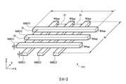
圖1為示出根據一些實施例的記憶體陣列的實例的方塊圖。1 is a block diagram illustrating an example of a memory array in accordance with some embodiments.
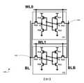
圖2為示出根據一些實施例的實例6T記憶胞的電路圖。2 is a circuit diagram illustrating an example 6T memory cell in accordance with some embodiments.
圖3為示出根據一些實施例的實例半導體結構的橫截面的方塊圖。3 is a block diagram illustrating a cross-section of an example semiconductor structure in accordance with some embodiments.
圖4為示出根據一些實施例的實例互連金屬層結構的方塊圖。4 is a block diagram illustrating an example interconnect metal layer structure in accordance with some embodiments.
圖5為示出根據一些實施例的實例互連金屬層結構的橫截面的方塊圖。5 is a block diagram illustrating a cross-section of an example interconnect metal layer structure in accordance with some embodiments.
圖6為示出根據一些實施例的實例半導體結構的橫截面的方塊圖。6 is a schematic diagram illustrating a cross-section of an example semiconductor structure in accordance with some embodimentsblock diagram.
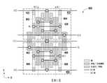
圖7為示出根據一些實施例的實例4Cpp FinFET SRAM胞單元的佈局圖。7 is a layout diagram illustrating an Example 4 Cpp FinFET SRAM cell in accordance with some embodiments.
圖8為示出根據一些實施例的實例4Cpp FinFET SRAM胞單元的電路圖。8 is a circuit diagram illustrating an Example 4 Cpp FinFET SRAM cell in accordance with some embodiments.
圖9為示出根據一些實施例的記憶胞單元陣列的實例陣列的方塊圖。9 is a block diagram illustrating an example array of memory cell arrays in accordance with some embodiments.
圖10為示出根據一些實施例的記憶胞單元陣列的另一實例陣列的方塊圖。10 is a block diagram illustrating another example array of memory cell arrays in accordance with some embodiments.
圖11為示出根據一些實施例的實例4Cpp FinFET SRAM胞單元的佈局圖。11 is a layout diagram illustrating an Example 4 Cpp FinFET SRAM cell in accordance with some embodiments.
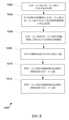
圖12為形成根據一些實施例的4Cpp FinFET SRAM胞單元的實例方法。12 is an example method of forming a 4Cpp FinFET SRAM cell in accordance with some embodiments.
以下揭露內容提供用於實施所提供主題的不同特徵的許多不同實施例或實例。下文描述組件及佈置的特定實例以簡化本揭露。當然,此等特定實例僅為實例且不意欲為限制性的。舉例而言,在以下描述中,第一特徵在第二特徵上方或第二特徵上形成可包含第一特徵與第二特徵直接接觸地形成的實施例,且亦可包含可在第一特徵與第二特徵之間形成額外特徵以使得第一特徵與第二特徵可不直接接觸的實施例。另外,本揭露可在各種實例中重複圖式元件標號及/或字母。此重複是出於簡單及清楚的目的,且自身並不指示所論述的各種實施例及/或組態之間的關係。The following disclosure provides many different embodiments or examples for implementing different features of the provided subject matter. Specific examples of components and arrangements are described below to simplify the present disclosure. Of course, these specific examples are merely examples and are not intended to be limiting. For example, in the following description, the formation of a first feature over or on a second feature may include embodiments in which the first feature is formed in direct contact with the second feature, and may also include embodiments that may be formed between the first feature and the second feature. Embodiments in which additional features are formed between the second features such that the first feature and the second feature may not be in direct contact. Additionally, the present disclosure may repeat drawing element numbers and/or letters in various instances. This repetition is for the purpose of simplicity and clarity, and does not in itself indicate a relationship between the various embodiments and/or configurations discussed.
此外,為易於描述,本文中可使用諸如「在......之下(beneath)」、「在......下方(below)」、「下部(lower)」、「在......之上(above)」、「上部(upper)」以及類似者的空間相對術語來描述如圖式中所示出的一個元件或特徵與另一元件或特徵的關係。除諸圖中所描繪的定向以外,空間相對術語意欲涵蓋元件在使用或操作中的不同定向。裝置可以其他方式定向(旋轉90度或處於其他定向),且本文中所使用的空間相對描述詞可同樣相應地進行解譯。Also, for ease of description, terms such as "beneath", "below", "lower", "below" may be used herein. Spatially relative terms such as "above", "upper" and the like are used to describe the relationship of one element or feature to another element or feature as illustrated in the figures. In addition to the orientation depicted in the figures, spatially relative terms are intended to encompass different orientations of elements in use or operation. The device may be otherwise oriented (rotated 90 degrees or at other orientations) and the spatially relative descriptors used herein interpreted accordingly.
靜態隨機存取記憶體(SRAM)元件具有記憶胞陣列,所述記憶胞陣列包含使用鰭式場效電晶體(FinFET)架構形成的電晶體。舉例而言,多晶矽結構可連接至在隔離材料上方延伸的半導體鰭。多晶矽結構充當FinFET電晶體的閘極,以使得施加至多晶矽結構的電壓決定連接至多晶矽結構的相對側上的鰭的源極/汲極(S/D)觸點之間的電子的流動。FinFET電晶體的臨界電壓為最小電壓,以使電晶體被視為「導通」,並使得可觀的電流可在S/D觸點之間流動。沿著鰭的長度且與鰭接觸的用於形成SRAM胞的多晶矽結構的數目可視為SRAM胞沿一個維度的「間距」,通常稱為「觸點多間距」或Cpp,且至少部分地決定了SRAM元件的密度。舉例而言,四觸點多間距(4Cpp)SRAM胞包含全部使用數個鰭形成的兩個傳輸閘極電晶體、兩個PMOS電晶體以及兩個NMOS電晶體,所述鰭具有沿其長度連接至鰭的四個多晶矽結構且具有連接至至少一些多晶矽結構之間的鰭的S/D觸點。Static random access memory (SRAM) devices have arrays of memory cells that include transistors formed using a fin field effect transistor (FinFET) architecture. For example, polysilicon structures may be connected to semiconductor fins extending over isolation material. The polysilicon structure acts as the gate of the FinFET transistor such that the voltage applied to the polysilicon structure determines the flow of electrons between source/drain (S/D) contacts connected to the fins on opposite sides of the polysilicon structure. The threshold voltage of a FinFET transistor is the minimum voltage for the transistor to be considered "on" and to allow appreciable current to flow between the S/D contacts. The number of polysilicon structures used to form the SRAM cell along the length of the fin and in contact with the fin can be considered as the "pitch" of the SRAM cell along one dimension, commonly referred to as "contact multi-pitch" or Cpp, and determines at least in part Density of SRAM elements. For example, a four-contact multi-pitch (4Cpp) SRAM cell includes two pass gate transistors, two PMOS transistors, and two NMOS transistors all formed using several fins with connections along their lengths Four polysilicon structures to the fins and have S/D contacts connected to the fins between at least some of the polysilicon structures.
在典型2Cpp FinFET SRAM架構的製造中,需要切割每個胞中的鰭的一部分的製程步驟才能形成6T SRAM胞。另外,在形成陣列中的每個胞的第一組觸點之後,需要額外處理步驟來形成某些共用觸點,所述共用觸點將記憶胞的第一反相器的第一對上拉/下拉電晶體的閘極連接至記憶胞的第二反相器的第二對電晶體的源極/汲極,以便形成交叉耦合的6T胞。這些共用觸點需要後續處理步驟,此是因為其在與源極/漏極觸點的正交方向上連接了胞組件,例如鰭、多晶矽以及觸點。In the fabrication of a typical 2Cpp FinFET SRAM architecture, a process step of cutting a portion of the fin in each cell is required to form a 6T SRAM cell. In addition, inAfter forming the first set of contacts for each cell in the array, additional processing steps are required to form certain common contacts that will memorize the first pair of pull-up/pull-down transistors of the first inverter of the cell. The gate of the memory cell is connected to the source/drain of the second pair of transistors of the second inverter of the memory cell to form a cross-coupled 6T cell. These common contacts require subsequent processing steps because they connect cell components such as fins, polysilicon, and contacts in an orthogonal direction to the source/drain contacts.
替代FinFET SRAM架構為4Cpp架構,其不需要切割每個胞中的鰭的一部分,且不需要具有後續處理步驟的共用觸點。然而,典型4Cpp架構導致擁擠的金屬層設計,例如位元線及互補位元線在同一跡線上運作,因此需要佈線設計解決方案及額外處理步驟才能在金屬層中實施這些解決方案。An alternative FinFET SRAM architecture is a 4Cpp architecture, which does not require cutting a portion of the fin in each cell, and does not require common contacts with subsequent processing steps. However, typical 4Cpp architectures result in crowded metal layer designs, such as bit lines and complementary bit lines operating on the same trace, thus requiring routing design solutions and additional processing steps to implement these solutions in the metal layers.
在本文中所揭露的一些實施例中,提供一種4Cpp FinFET SRAM架構,所述架構不需要切割每個胞中的鰭的一部分,不需要共用觸點,且簡化金屬層佈線。在一些實施例中,4Cpp胞包括共用位元線及互補位元線的兩個4Cpp位元胞。In some embodiments disclosed herein, a 4Cpp FinFET SRAM architecture is provided that does not require cutting a portion of the fin in each cell, does not require common contacts, and simplifies metal layer routing. In some embodiments, a 4Cpp cell includes two 4Cpp bit cells that share a bit line and a complementary bit line.
圖1為示出根據一些實施例的記憶體陣列10的一實例的方塊圖。圖1繪示具有多個記憶胞100或位元胞100的記憶體陣列10。一或多個周邊電路(圖中未示)可位於記憶體陣列10周邊或所述記憶體陣列內的一或多個區域處。記憶胞100與周邊電路可藉由互補位元線BL及互補位元線BLB耦合,且資料可經由互補位元線BL及互補位元線BLB讀取自及寫入至記憶胞100。FIG. 1 is a block diagram illustrating an example of a
圖2為示出根據一些實施例的實例記憶胞100的電路圖。記憶胞100包含但不限於六電晶體(six-transistor;6T)SRAM結構。在一些實施例中,可使用多於或少於六個電晶體來實施記憶胞100。舉例而言,記憶胞100在一些實施例中可使用4T SRAM結構、8T SRAM結構或10T SRAM結構,且在其他實施例中可包含記憶體類的位元胞或構建單元。記憶胞100包含由NMOS/PMOS電晶體對PU0與PD0(例如上拉電晶體0與下拉電晶體0)形成的第一反相器。記憶胞100亦包含由NMOS/PMOS電晶體對PU1與PD1形成的第二反相器以及存取電晶體/傳輸閘極PG0及PG1。電晶體PD0、電晶體PD1、電晶體PG0以及電晶體PG1包含n型金屬氧化物半導體(n-type metal-oxide-semiconductor;NMOS)電晶體,且電晶體PU0及電晶體PU1包含p型金屬氧化物半導體(p-type metal-oxide semiconductor;PMOS)電晶體。FIG. 2 is a circuit diagram illustrating an
將電源供應至每一反相器中,例如,電晶體PU0及電晶體PU1中之每一者的第一端子耦合至電源供應VDD,而電晶體PD0及電晶體PD1中之每一者的第一端子耦合至參考電壓VSS,例如接地。資料的一個位元(bit)儲存於記憶胞100中以作為節點Q處的電壓電平,且可由電路經由位元線BL讀取。對節點Q的存取受到傳輸閘極電晶體PG0控制。節點Qbar(
傳輸閘極電晶體PG0的閘極耦合至字元線WL。傳輸閘極電晶體PG0的第一源極/汲極(S/D)端子耦合至位元線BL,且傳輸閘極電晶體PG0的第二S/D端子耦合至電晶體PU0及電晶體PD0在節點Q處的第二端子。The gate of pass gate transistor PG0 is coupled to word line WL. A first source/drain (S/D) terminal of pass gate transistor PG0 is coupled to bit line BL, and a second S/D terminal of pass gate transistor PG0 is coupled to transistors PU0 and PD0 A second terminal at node Q.
類似地,傳輸閘極電晶體PG1的閘極耦合至字元線WL。傳輸閘極電晶體PG1的第一S/D端子耦合至互補位元線BLB,且傳輸閘極電晶體PG1的第二S/D第一端子耦合至電晶體PU1及電晶體PD1在節點Qbar處的第二端子。Similarly, the gate of pass gate transistor PG1 is coupled to word line WL. The first S/D terminal of pass gate transistor PG1 is coupled to complementary bit line BLB, andThe second S/D first terminal of pass gate transistor PG1 is coupled to the second terminals of transistor PU1 and transistor PD1 at node Qbar.
圖3為示出根據一些實施例的實例半導體結構的橫截面的方塊圖。在X軸及Z軸方向上繪示結構20,而Y軸方向與圖3中所示出的橫截面的平面正交。結構20包含基層110及互連層120。3 is a block diagram illustrating a cross-section of an example semiconductor structure in accordance with some embodiments. The
一般而言,基層110包含半導體基底,半導體基底又包含多晶矽區域(例如在本揭露中亦稱為「多晶矽(poly)」)、擴散區域、半導體阱(例如N阱、P阱、深N阱、深P阱)等,其中形成了半導體元件(例如電晶體、二極體等)。互連層120包含N個(例如整數個)導電層(例如金屬層M1至金屬層MN),其用於互連互連層120中的層內的元件並用於形成電性連接至外部元件等。互連層120大致上包含通孔、層級間介電材料、鈍化層、接合墊、封裝資源等。互連層120中的各金屬(例如導電)層M通常稱作金屬一層(M1)、金屬二層(M2)、金屬三層(M3)等。介電材料(例如高介電常數材料、低介電常數材料等)130位於各種金屬層M之間用以使金屬層M絕緣。基層110及互連層120通常分別被稱作前段結構及後段結構,這是因為其為半導體製作製程中的各別「前段生產線」(front end of line;FEOL)及「後段生產線(back end of line;BEOL)」。在一些實施例中,包含記憶胞、鎖定器(latches)以及正反器(flip-flops)的記憶體或儲存元件使用基層110及金屬層M中的一或多者來構建。Generally, the
圖4為示出根據一些實施例的實例互連金屬層結構200的方塊圖。金屬層結構200包含多個導電層M(例如M1、M2、M3等)。在所示實施例中,金屬層結構200示出僅兩個層(例如M2及M3),且繪示於圖5中且進一步在下文描述的實施例示出具有四個層(例如M1、M2、M3以及M4)的金屬層結構200的橫截面視圖。繪示於圖4及圖5中的層的數目用於示例,且具有不同數量的層(例如1至N個層)的金屬層結構200亦在所揭露實施例的範圍內。4 is a block diagram illustrating an example interconnect
在圖4中所示的實施例中,每一金屬層M包含層M2中的多個金屬條MB,例如金屬條MB21、金屬條MB22以及金屬條MB23;及層M3中的金屬條MB31、金屬條MB32、金屬條MB33。在一些實施例中,金屬條的形狀為圓柱形或一些其他形狀,且可為任何橫截面形狀。在所示實施例中,層M中的金屬條MB中之每一者實質上彼此平行。在所示實施例中,每一金屬層M2及金屬層M3包含三個金屬條MB,然而,每個金屬層M具有不同數目個金屬條MB的組態亦在所揭露實施例的範圍內。在一些實施例中,第一組金屬條MB(例如金屬層M1、金屬層M3、金屬層M5等中的金屬條MB)在第一方向(例如X軸方向)上延伸,而(例如金屬層M2、金屬層M4、金屬層M6等中的)第二組金屬條MB在第二方向(例如Y軸方向)上延伸,其中X軸方向垂直於Y軸方向。其中所有條MB在一個方向(例如X軸方向、Y軸方向或任何其他適宜的方向或方向的組合,包含非垂直方向)上延伸的不同組態亦在所揭露實施例的範圍內。在圖4中所示的實施例中,每一金屬條MB具有寬度Wbar。在一些實施例中,所有寬度Wbar具有相同尺寸,但所揭露實施例不限於此組態。視設計選擇而定,寬度Wbar可具有不同尺寸(例如一個寬度Wbar可短於/大於另一個)。兩個相鄰金屬條MB以例如距離D的距離間隔或分離。在一些實施例中,距離D經選擇為符合兩個金屬條MB之間的間距的最小值要求以在這些兩個條之間形成電容。在一些實施例中,金屬層結構200中的所有距離D具有相同尺寸,但所揭露實施例不限於此組態。亦即,距離D可具有不同尺寸(例如一個距離D可短於/長於另一個)。層M中的金屬條MB的厚度與層M厚度成比例,其可取決於製程技術,且不同組的層M可具有不同厚度。舉例而言,第一組的金屬層M(例如Mx)可具有第一厚度,第二組的金屬層M(例如My)可具有第二厚度,且金屬層的第三組(例如Mz)可具有第三厚度等,其中第一厚度、第二厚度以及第三厚度不同。在所示實施例中,金屬層結構200具有寬度W及長度L。In the embodiment shown in FIG. 4, each metal layer M includes a plurality of metal bars MB in layer M2, such as metal bar MB21, metal bar MB22 and metal bar MB23; and metal bar MB31, metal bar in layer M3 Strip MB32, metal strip MB33. In some embodiments, the shape of the metal strip is cylindrical or some other shape, and can be any cross-sectional shape. In the embodiment shown, each of the metal strips MB in layer M is substantially parallel to each other. In the illustrated embodiment, each metal layer M2 and metal layer M3 includes three metal bars MB, however, configurations where each metal layer M has a different number of metal bars MB are also within the scope of the disclosed embodiments. In some embodiments, the first set of metal stripes MB (eg, metal strips MB in metal layer M1, metal layer M3, metal layer M5, etc.) extend in a first direction (eg, the X-axis direction), while (eg, metal layer A second group of metal strips MB in M2, metal layer M4, metal layer M6, etc.) extends in a second direction (eg, a Y-axis direction), where the X-axis direction is perpendicular to the Y-axis direction. Different configurations in which all bars MB extend in one direction (eg, the X-axis direction, the Y-axis direction, or any other suitable direction or combination of directions, including non-perpendicular directions) are also within the scope of the disclosed embodiments. In the embodiment shown in FIG. 4, each metal bar MB has a width Wbar. In some embodiments, all widths Wbar have the same size, but the disclosed embodiments are not limited to this configuration. Depending on design choices, the width Wbar can have different dimensions (eg one width Wbar can be shorter/greater than the other)indivual). Two adjacent metal strips MB are spaced or separated by a distance such as a distance D. In some embodiments, the distance D is selected to meet the minimum requirement for the spacing between the two metal strips MB to form a capacitance between the two strips. In some embodiments, all distances D in the
圖5為示出根據一些實施例的實例互連金屬層結構200的橫截面的方塊圖。在所示實施例中,金屬層結構200包含具有平行於X軸定向的金屬條MB的金屬層M1及金屬層M3,所述金屬條例如金屬跡線、導線、導體等;以及具有平行於Y軸且與M1金屬條及M3金屬條正交定向的金屬條MB的金屬層M2及金屬層M4。在所示實施例中,金屬層M藉由介電材料130分離。5 is a block diagram illustrating a cross-section of an example interconnect
圖6為示出根據一些實施例的實例半導體結構300的橫截面的方塊圖。所示實施例包含具有半導體結構的FEOL層以及具有互連金屬層結構的BEOL層。6 is a block diagram illustrating a cross-section of an
在所示實施例中,FEOL層示出傳輸閘極FinFET電晶體310。FinFET電晶體310包含半導體基底、鰭、隔離區域、多晶矽結構(例如多晶矽)、連接至鰭的導電觸點S及導電觸點D以及連接至多晶矽結構的導電G觸點。在所示實施例中,電流的傳導路徑為鰭(鰭亦可稱為擴散區域或氧化物擴散區域)。多晶矽結構充當閘極,從而允許在鰭中的電流自S(例如源極)觸點流向D(例如汲極)觸點。舉例而言,對於S觸點與D觸點之間的電壓電位,電流可在鰭中自S流動至D是取決於施加至多晶矽結構的電壓而定。若將小於臨界電壓的電壓施加至多晶矽,則不能夠使可觀的電流在鰭中自S觸點流動至D觸點,而電晶體310為「關閉(off)」。若將大於或等於臨界電壓的電壓施加至多晶矽,則可觀的電流經由鰭自S流動至D,而電晶體310為「開啟(on)」。在一些實施例中,S觸點、D觸點以及G觸點在FEOL層中的多個鰭與多晶矽結構之間形成連接,藉此連接一或多個電晶體的源極、汲極以及閘極。在一些實施例中,電晶體310的源極、汲極以及閘極連接至BEOL層中的互連金屬層結構。舉例而言,通常電晶體310的閘極連接至字元線,所述字元線為BEOL層中的互連金屬結構的層中的一者中的金屬條中的一者,且傳輸閘極電晶體310的S/D觸點將類似地連接至互補位元線BL及BLB,所述互補位元線BL及BLB為BEOL層中的金屬層中的一或多者中的金屬條的其他者。在一些實施例中,BEOL層用以將電晶體310連接至周邊電路,例如用於讀取/寫入操作。在所示實施例中,D觸點及G觸點使用通孔連接至BEOL層中的金屬條。舉例而言,Via1在D觸點至金屬條(例如位元線)之間形成連接,其中所述金屬條位於FEOL層上方的第一金屬層M1中。在所示實施例中,獨立的Via1將G觸點連接至M1層中的導電著陸墊,且Via2將導電著陸墊連接至M2層中的金屬條(例如字元線)。在一些實施例中,M1層中的導電著陸墊可由已在其金屬層的平面內經切割或斷開連接的金屬條所形成。舉例而言,導電著陸墊可由如圖5中所示出的金屬條MB11的金屬條形成,其中MB11已沿其在X軸方向上的長度在對應於其上方的金屬層中的MB22金屬條的任一側上的D的位置中經切割或斷開連接,從而形成導電隔離的短金屬條或接墊。In the illustrated embodiment, the FEOL layer shows the pass
圖7為示出根據一些實施例的實例4Cpp FinFET SRAM胞單元400的佈局圖。4Cpp FinFET SRAM胞單元400包含第一4Cpp記憶體位元胞,例如第一位元胞410以及第二位元胞450。圖7中示出的實施例亦包含第一金屬層(例如,如圖5中所示出的M1)中的金屬線及第二金屬層(例如,如圖5中所示出的M2)中的金屬線。在所示實施例中,第一位元胞410及第二位元胞450中之每一者形成了6T SRAM記憶胞,例如上述關於圖2所描述的記憶胞100,其包含電晶體PG0、電晶體PU0、電晶體PD0、電晶體PG1、電晶體PU1以及電晶體PD1。7 is a layout diagram illustrating an Example 4 Cpp
在所示實施例中,第一位元胞410包含鰭412及鰭414;多晶矽結構422、多晶矽結構424、多晶矽結構426以及多晶矽結構428;以及S/D觸點432、S/D觸點434以及S/D觸點436。第一位元胞410亦包含將FEOL層中的第一位元胞410的組件連接至BEOL層中的導線或跡線(例如金屬條)的通孔441、442、443、444、445、446、447、448。在所示實施例中,鰭412及鰭414沿第一方向(例如,如圖7中所示的X軸方向)具有較長尺寸(例如長度),且在第二方向(例如,Y軸方向)上彼此分離。多晶矽結構422至多晶矽結構428及S/D觸點432至S/D觸點436沿第二方向(例如,如圖7中所示的Y軸方向)具有較長尺寸(例如長度),且在第一方向(例如X軸方向)上彼此分離。在一些實施例中,鰭、多晶矽以及S/D觸點的長度具有並非其最長尺寸的長度,例如鰭、多晶矽以及S/D觸點可具有正方形、橢圓形、圓形或任何其他形狀。In the embodiment shown,
在所示實施例中,將電源供應至第一金屬層M1中的VDD線,且藉由通孔441將所述電源連接至第一位元胞410的電晶體PU0及電晶體PU1兩者的S/D觸點434。S/D觸點434在多晶矽結構424旁但不與多晶矽結構424接觸,而是連接至鰭412。多晶矽424亦連接至鰭412。S/D觸點432在與S/D觸點434相對的多晶矽424的相對側上(例如在負X軸方向上)且位於多晶矽424旁但不與多晶矽424接觸,而是連接至鰭412。S/D觸點434、鰭412、多晶矽424以及S/D觸點432形成PU0電晶體,其中S/D觸點434及S/D觸點432作為源極及汲極,且多晶矽424作為閘極。PU1電晶體由全部連接至鰭412的S/D觸點434、S/D觸點436以及多晶矽426形成,其中S/D觸點436在多晶矽426旁但不與多晶矽426接觸,且在與S/D觸點434相對的多晶矽426的相對側上。In the illustrated embodiment, power is supplied to the VDD line in the first metal layer M1, and the power is connected to both transistors PU0 and PU1 of the
在所示實施例中,S/D觸點432及S/D觸點436在第二方向上(例如在負Y軸上)自鰭412延伸且連接至鰭414。多晶矽結構424及多晶矽結構426類似地在第二方向上延伸且連接至鰭414。在所示實施例中,第二方向大體上與第一方向正交,且S/D觸點432、S/D觸點436以及多晶矽424及多晶矽426在鰭414上重複其如同鰭412的置放,也就是說,S/D觸點432、多晶矽424、多晶矽426以及S/D觸點436在正X軸方向上。在所示實施例中,S/D觸點404連接至多晶矽424與多晶矽426之間的鰭414,且藉由通孔494連接至M1金屬層中的VSS。S/D觸點432、鰭414、多晶矽424以及S/D觸點404形成PD0電晶體,其中S/D觸點432及S/D觸點404作為源極及汲極,且多晶矽424作為閘極。類似地,在正X軸方向上沿鰭414,PD1電晶體由全部連接至鰭414的S/D觸點404、多晶矽426以及S/D觸點436形成。在所示實施例中,PD0電晶體與PD1電晶體共用S/D觸點404,且藉此連接至M1層中的參考電壓VSS,例如接地。多晶矽424為PU0電晶體及PD0電晶體兩者的閘極,且如此,PU0電晶體與PD0電晶體的閘極如圖2中所示般連接。類似地,多晶矽426為PU1電晶體及PD1電晶體兩者的閘極,且如此,PU1電晶體與PD1電晶體的閘極如圖2中所示般連接。In the illustrated embodiment, S/
在所示實施例中,多晶矽422連接至S/D觸點432與S/D觸點402之間的鰭414,S/D觸點432與S/D觸點402亦各自連接至鰭414,從而形成傳輸閘極電晶體PG0。S/D觸點402藉由通孔492連接至M1金屬層中的位元線BL,藉此將電晶體PG0的源極/汲極端子連接至位元線BL。類似地,多晶矽428連接至S/D觸點436與S/D觸點406之間的鰭414,S/D觸點436與S/D觸點406亦各自連接至鰭414,從而形成傳輸閘極電晶體PG1。S/D觸點406藉由通孔496連接至M1金屬層中的互補位元線BLB,藉此將電晶體PG1的源極/汲極端子連接至互補位元線BLB。In the embodiment shown,
在所示實施例中,多晶矽426藉由M1層中的導線連接至S/D觸點432。在所示實例中,藉由以下操作來形成此連接:藉由通孔443將多晶矽426連接至M1層中的導線,以及藉由通孔442將S/D觸點432連接至M1層中的導線。如此,如圖2中所示出,PU1電晶體及PD1電晶體的閘極在節點Q處連接至PU0電晶體、PD0電晶體以及PG0電晶體中之每一者的S/D端子。類似地,多晶矽424藉由M1層中的導線連接至S/D觸點436。在所示實例中,藉由以下操作來形成此連接:藉由通孔447將多晶矽424連接至M1層中的導線,以及藉由通孔448將S/D觸點436連接至M1層中的導線。如此,如圖2中所示出,PU0電晶體及PD0電晶體的閘極在互補節點Qbar處連接至PU1電晶體、PD1電晶體以及PG1電晶體中之每一者的S/D端子。In the embodiment shown, the
在所示實施例中,多晶矽422與多晶矽428(例如PG0電晶體與PG1電晶體的閘極)由M1層中的導線連接。在所示實例中,藉由以下操作來形成此連接:藉由通孔444將多晶矽422連接至M1層中的導線,以及藉由通孔446將多晶矽428連接至M1層中的導線。M1層中的導線藉由通孔445連接至M2層中的導線,例如字元線WL0。如此,在所示實施例中,PG0電晶體及PG1電晶體的兩個閘極連接至如圖2中所示出的字元線WL0。在所示實施例中,連接PG0及PG1的閘極的第一金屬層M1中的導線具有與第二金屬層M2中的導線(例如字元線WL0)的長度尺寸正交的長度尺寸。In the embodiment shown,
在所示實施例中,第二位元胞450包含鰭452及鰭454、多晶矽結構462、多晶矽結構464、多晶矽結構466以及多晶矽結構468以及S/D觸點472、S/D觸點474以及S/D觸點476。第二位元胞450亦包含將FEOL層中的第二位元胞450的組件連接至BEOL層中的導線或跡線(例如金屬條)的通孔481、482、483、484、485、486、487、488。在所示實施例中,鰭452及鰭454沿第一方向(例如,如圖7中所示的X軸方向)具有較長尺寸(例如長度),且在第二方向(例如Y軸方向)上彼此分離。多晶矽結構462至468及S/D觸點472至S/D觸點476沿第二方向(例如,如圖7中所示的Y軸方向)具有較長尺寸(例如長度),且在第一方向(例如X軸方向)上彼此分離。在一些實施例中,鰭、多晶矽以及S/D觸點的長度具有不為其最長尺寸的長度,例如鰭、多晶矽以及S/D觸點可具有正方形、橢圓形、圓形或任何其他形狀。In the embodiment shown,
在所示實施例中,將電源供應至第一金屬層M1中的VDD線,且藉由通孔481將所述電源連接至第二位元胞450的電晶體PU0及電晶體PU1兩者的S/D觸點474。S/D觸點474在多晶矽結構464旁但不與多晶矽結構464接觸,而是連接至鰭452。多晶矽464亦連接至鰭452。S/D觸點472在與S/D觸點474相對的多晶矽464的相對側上(例如在負X軸方向上)且位於多晶矽464旁但不與多晶矽464接觸,而是連接至鰭452。S/D觸點474、鰭452、多晶矽464以及S/D觸點472形成PU0電晶體,其中S/D觸點474及S/D觸點472作為源極及汲極,且多晶矽464作為閘極。PU1電晶體由全部連接至鰭452的S/D觸點474、S/D觸點476以及多晶矽466形成,其中S/D觸點476在多晶矽466旁但不與多晶矽466接觸,且在與S/D觸點474相對的多晶矽466的相對側上。In the illustrated embodiment, power is supplied to the VDD line in the first metal layer M1, and the power is connected to both transistors PU0 and PU1 of the
在所示實施例中,S/D觸點472及S/D觸點476在第二方向上(例如在正Y軸上)自鰭452延伸且連接至鰭454。多晶矽結構464及多晶矽結構466類似地在第二方向上延伸且連接至鰭454。在所示實施例中,第二方向大體上與第一方向正交,且S/D觸點472、S/D觸點476以及多晶矽464及多晶矽466在鰭454上重複其如同鰭452的置放,也就是說,S/D觸點472、多晶矽464、多晶矽466以及S/D觸點476在正X軸方向上。在所示實施例中,S/D觸點404在負Y軸方向上自鰭414延伸,且連接至多晶矽464與多晶矽466之間的鰭454,且藉由如上文所描述的通孔494連接至M1金屬層中的VSS。如此,第一位元胞410與第二位元胞「共用」S/D觸點404。S/D觸點472、鰭454、多晶矽464以及S/D觸點404形成PD0電晶體,其中S/D觸點472及S/D觸點404作為源極及汲極,且多晶矽464作為閘極。類似地,在正X軸方向上沿鰭454,PD1電晶體由全部連接至鰭454的S/D觸點404、多晶矽466以及S/D觸點476形成。在所示實施例中,PD0電晶體與PD1電晶體共用S/D觸點404,且藉此連接至M1層中的參考電壓VSS,例如接地。多晶矽464為PU0電晶體及PD0電晶體兩者的閘極,且如此,PU0電晶體與PD0電晶體的閘極如圖2中所示般連接。類似地,多晶矽466為PU1電晶體及PD1電晶體兩者的閘極,且如此,PU1電晶體與PD1電晶體的閘極如圖2中所示般連接。In the illustrated embodiment, S/
在所示實施例中,多晶矽462連接至S/D觸點472與S/D觸點402之間的鰭454,S/D觸點472與S/D觸點402亦各自連接至鰭454,從而形成傳輸閘極電晶體PG0。在所示實施例中,S/D觸點402在負Y軸方向上自鰭414延伸,且連接至鰭454,且藉由如上文所描述的通孔492連接至M1金屬層中的位元線BL,藉此將電晶體PG0的源極/汲極端子連接至位元線BL。如此,第一位元胞410與第二位元胞「共用」S/D觸點402,且亦共用位元線BL。類似地,多晶矽468連接至S/D觸點476與S/D觸點406之間的鰭454,S/D觸點476與S/D觸點406亦各自連接至鰭414,從而形成傳輸閘極電晶體PG1。在所示實施例中,S/D觸點406在負Y軸方向上自鰭414延伸,且連接至鰭454,且藉由如上文所描述的通孔496連接至M1金屬層中的互補位元線BLB,藉此將電晶體PG1的源極/汲極端子連接至互補位元線BLB。如此,第一位元胞410與第二位元胞「共用」S/D觸點406,且亦共用互補位元線BLB。In the embodiment shown,
在所示實施例中,多晶矽464藉由M1層中的導線連接至S/D觸點476。在所示實例中,藉由以下操作來形成此連接:藉由通孔483將多晶矽464連接至M1層中的導線,以及藉由通孔482將S/D觸點476連接至M1層中的導線。如此,如圖2中所示,PU0電晶體及PD0電晶體的閘極在節點Qbar處連接至PU1電晶體、PD1電晶體以及PG1電晶體中之每一者的S/D端子。類似地,多晶矽466藉由M1層中的導線連接至S/D觸點472。在所示實例中,藉由以下操作來形成此連接:藉由通孔487將多晶矽466連接至M1層中的導線,以及藉由通孔488將S/D觸點472連接至M1層中的導線。如此,如圖2中所示出,PU1電晶體及PD1電晶體的閘極在互補節點Q處連接至PU0電晶體、PD0電晶體以及PG0電晶體中之每一者的S/D端子。In the embodiment shown,
在所示實施例中,多晶矽462與多晶矽468(例如PG0電晶體與PG1電晶體的閘極)由M1層中的導線連接。在所示實例中,藉由以下操作來形成此連接:藉由通孔484將多晶矽462連接至M1層中的導線,以及藉由通孔486將多晶矽468連接至M1層中的導線。M1層中的導線藉由通孔485連接至M2層中的導線,例如字元線WL0。如此,在所示實施例中,PG0電晶體及PG1電晶體的兩個閘極連接至字元線WL1。在所示實施例中,連接PG0及PG1的閘極的第一金屬層M1中的導線具有與第二金屬層M2中的導線(例如字元線WL1)的長度尺寸正交的長度尺寸。In the embodiment shown,
如上文所描述,在圖7中所示的實例中,S/D觸點402、S/D觸點404以及S/D觸點406在4Cpp FinFET SRAM胞單元400的第一位元胞420與第二位元胞450之間共用。如此,S/D觸點402、S/D觸點404以及S/D觸點406可被視為第一位元胞410及第二位元胞450兩者的一部分。在一些實施例中,不需要額外或後續處理步驟來形成共用S/D觸點402、共用S/D觸點404以及共用S/D觸點406。As described above, in the example shown in FIG. 7 , S/
在圖7中所示的實例中,位元線BL及互補位元線BLB處於不同「跡線」,例如相同金屬層M1中的不同線,從而降低BEOL金屬層中的擁塞。舉例而言,在一些實施例中,在圖4及圖5中所示的圖示的命名法中,位元線BL對應於金屬條MB11,且互補位元線BLB對應於金屬條MB21。在一些實施例中,4Cpp FinFET SRAM胞單元400不需要切割鰭結構或區域。在一些實施例中,4Cpp FinFET SRAM胞單元400不需要某些共用觸點,例如需要後續處理步驟的共用觸點,此是因為所述共用觸點在與源極/汲極觸點正交的方向上連接胞組件,例如鰭、多晶矽以及S/D觸點。In the example shown in Figure 7, bit line BL and complementary bit line BLB are on different "traces", eg, different lines in the same metal layer Ml, thereby reducing congestion in the BEOL metal layer. For example, in some embodiments, in the nomenclature of the diagrams shown in FIGS. 4 and 5, bit line BL corresponds to metal bar MB11, and complementary bit line BLB corresponds to metal bar MB21. In some embodiments, the 4Cpp
圖8為示出根據一些實施例的實例4Cpp FinFET SRAM胞單元400的電路圖。圖8中所示的實例大體上對應於圖2中所示出的兩個6T SRAM胞,所述6T SRAM胞經佈置為連接至如圖1中所示的記憶體陣列10的記憶體陣列的列或行中的相同位元線BL及互補位元線BLB。在所示實例中,4Cpp FinFET SRAM胞單元400包含第一位元胞410及第二位元胞450。圖8中所示的實例表示圖7中所示出的FinFET佈局結構的電路圖。在所示實例中,共用連接點492將第一位元胞410及第二位元胞450連接至如圖7中所示出的位元線BL。類似地,共用連接點496將第一位元胞410及第二位元胞450連接至如圖7中所示出的互補位元線BLB。8 is a circuit diagram illustrating an Example 4 Cpp
圖9為示出根據一些實施例的記憶胞單元陣列的實例陣列600的方塊圖。陣列600包含以3×3網格圖案(grid pattern)佈置的九個記憶胞400。在所示實例中,記憶胞400對應於4Cpp FinFET SRAM胞單元400。圖9中所示的實例示出使用如4Cpp FinFET SRAM胞單元400的4Cpp FinFET SRAM架構的記憶體陣列元件的一個實例字元線及互補位元線佈置。9 is a block diagram illustrating an
在所示實施例中,位元胞410及位元胞450至位元線BL的連接藉由連接至共用S/D觸點402的通孔492來形成,共用S/D觸點402為位元胞410及位元胞450兩者的兩個傳輸閘極PG0電晶體的共用S/D觸點。類似地,位元胞410及位元胞450至互補位元線BLB的連接藉由連接至共用S/D觸點406的通孔496來形成,共用S/D觸點406為位元胞410及位元胞450兩者的兩個傳輸閘極PG1電晶體的共用S/D觸點。In the embodiment shown, the connection of
在所示實例中,在一行中的每一個位元胞410的字元線是共用的,且在一行中的每一個位元胞450的字元線是共用的。舉例而言,行C中的位元胞410的PG0電晶體及PG1電晶體的閘極中之每一者連接至WL1,且行C中的位元胞450的PG0電晶體及PG1電晶體的閘極中之每一者連接至WL0。類似地,在所示實例中,行B中的位元胞410連接至WL3,行B中的位元胞450連接至WL2,行A中的位元胞410連接至WL5,行A中的位元胞450連接至WL4。在所示實施例中,以每隔一個的方式連接至相鄰字元線的行中的每一位元胞,字元線佈置為「每隔一個」或「奇數-偶數」佈置。舉例而言,行C中的位元胞410中的全部連接至「奇數」字元線WL1,且行C中的位元胞450中的全部連接至「偶數」字元線WL0。在所示實施例中,行A及行B中的位元胞410類似地分別全部連接至「奇數」字元線WL5及WL3,且行A及行B中的位元胞450類似地分別全部連接至「偶數」字元線WL4及WL2。In the example shown, the word line for each
圖10為示出根據一些實施例的記憶胞單元陣列的另一實例陣列700的方塊圖。圖10中所示的實例表示對圖9中所示的字元線連接佈置的替代字元線連接佈置。10 is a block diagram illustrating another
在所示實施例中,參照連接至與相同行中的相鄰4Cpp FinFET SRAM胞單元400的第二位元胞450相同的字元線的第一4Cpp FinFET SRAM胞單元400的第一位元胞410,字元線佈置為「奇數-奇數、偶數-偶數」佈置。舉例而言,在所示實施例中,列1及行C中的胞單元400的第一位元胞410連接至與列2及行C中的胞單元400的第二位元胞450相同的字元線WL1。列2及行C中的胞單元400的第一位元胞410連接至與列3及行C中的胞單元400的第二位元胞450相同的字元線WL0,且所述圖案隨字元線連接在WL0與WL1之間切換而每兩個位元胞重複一次,所述位元胞在相鄰胞單元400中。In the embodiment shown, reference is made to the first bit cell of a first 4Cpp
圖11為示出根據一些實施例的實例4Cpp FinFET SRAM胞單元800的佈局圖。在所示實例中,4Cpp FinFET SRAM胞單元800包含連續氧化物限定邊緣上多晶矽(continuous poly on oxide definition edge;CPODE)圖案802、804、806以及808。Figure 11 is a diagram illustrating an Example 4Cpp FinFET SRAM in accordance with some embodimentsLayout of
在一些實施例中,當經由各種技術節點按比例縮小如金屬氧化物半導體場效電晶體(metal-oxide-semiconductor field-effect transistor;MOSFET)的半導體元件時,元件封裝密度及元件效能受到元件佈局及隔離挑戰。為避免相鄰元件(胞)之間的漏電,標準胞佈局採用形成於氧化矽限定(silicon oxide definition;OD)區域的邊緣上的虛設多晶矽區段,例如FinFET中的鰭,亦即OD邊緣上多晶矽(poly-on-OD-edge;PODE)。PODE有助於達成較佳元件效能及較佳多晶矽輪廓控制。鰭隔離結構在半導體鰭中具有氣隙以分離兩個相鄰胞,且具有介電頂蓋層以將氣隙的頂部封蓋以用於後續製程,如金屬著陸。氣隙具有極低的介電常數,且為極佳的電隔離器。因為在半導體鰭內形成氣隙,所以不需要額外區域來形成鰭隔離結構,且因此可縮小元件尺寸。In some embodiments, as semiconductor devices such as metal-oxide-semiconductor field-effect transistors (MOSFETs) are scaled down through various technology nodes, device packing density and device performance are affected by device layout and isolation challenges. To avoid leakage between adjacent elements (cells), standard cell layouts employ dummy polysilicon segments formed on the edges of silicon oxide definition (OD) regions, such as fins in FinFETs, on the OD edges Polysilicon (poly-on-OD-edge; PODE). PODE helps achieve better device performance and better polysilicon profile control. The fin isolation structure has an air gap in the semiconductor fin to separate two adjacent cells, and a dielectric capping layer to cap the top of the air gap for subsequent processes, such as metal landing. Air gaps have extremely low dielectric constants and are excellent electrical isolators. Because air gaps are formed within the semiconductor fins, no additional area is required to form the fin isolation structures, and thus device size can be reduced.
在一些實施例中,PODE結構在標準胞100的邊緣上形成,且用以在處理期間保護半導體鰭的末端。亦即,PODE多晶矽結構不電性連接為MOS元件的閘極,而是在電路中不具有功能的「虛設」結構。PODE結構覆蓋且保護胞中的鰭的末端,從而在處理期間提供額外的可靠性。In some embodiments, PODE structures are formed on the edges of
在一些實施例中,CPODE圖案或PODE圖案用以藉由移除虛設材料及半導體主體的部分以及甚至在虛設材料下的絕緣特徵的部分而形成溝槽。介電結構藉由用介電材料填充溝槽而形成,且CPODE圖案或PODE圖案無需額外罩幕。在一些實施例中,介電結構與形成如電容器的元件的其他部分中的其他CPODE結構同時形成。與形成其他CPODE結構同時形成介電結構有助於避免對額外罩幕的需要且降低生產成本。與其他方法相比,藉由使用CPODE或PODE圖案,降低了在胞之間導致雜訊增加、信號延遲、邏輯差錯以及積體電路故障的耦合效應。這是因為雜訊耦合路徑由於非導電材料而切斷。In some embodiments, a CPODE pattern or PODE pattern is used to form trenches by removing portions of the dummy material and the semiconductor body and even portions of insulating features under the dummy material. The dielectric structure is formed by filling the trenches with a dielectric material, and no additional mask is required for the CPODE pattern or PODE pattern. In some embodiments,The dielectric structure is formed concurrently with other CPODE structures in other parts of the element that form the capacitor. Forming the dielectric structure at the same time as other CPODE structures helps avoid the need for additional masks and reduces production costs. By using a CPODE or PODE pattern, coupling effects between cells that cause increased noise, signal delays, logic errors, and integrated circuit failures are reduced compared to other methods. This is because the noise coupling path is cut due to the non-conductive material.
在一些實施例中,可形成雙埠(dual-port;DP)4Cpp FinFET SRAM胞單元。舉例而言,4Cpp FinFET SRAM胞單元400的第一位元胞410及第二位元胞450可各自包含連接至第二位元線BL-2及第二互補位元線BL-2的兩個額外傳輸閘極電晶體。在一些實施例中,第二組互補位元線BL-2及互補位元線BLB-2可連接至不同周邊電路,藉此將至少兩個周邊電路連接至資料線,所述資料線可存取儲存於位元胞410及位元胞450中的資料並涉及位元胞410及位元胞450的讀取-寫入操作。在一些實施例中,對位元胞410及位元胞450的雙埠存取實現了對記憶體元件10的較快讀取-寫入速度。在一些實施例中,雙埠4Cpp FinFET SRAM胞單元中的兩個額外傳輸閘極電晶體可具有連接至第二組字元線(例如WL0-2及WL1-2)的閘極。與第二組互補位元線類似,第二組字元線可連接至不同周邊電路,藉此允許至少兩個周邊電路存取位元胞410及位元胞450中之每一者中的資料,且允許至少兩個周邊電路存取有關於位元胞410及位元胞450的讀取-寫入操作。在一些實施例中,雙埠位元線及連接可在第一位元胞410與第二位元胞450之間共用。In some embodiments, a dual-port (DP) 4Cpp FinFET SRAM cell can be formed. For example, the
圖12為形成根據一些實施例的4Cpp FinFET SRAM胞單元的實例方法1000。方法1000在步驟1002處開始,其中在第一位元胞及第二位元胞中形成多晶矽結構。舉例而言,多晶矽422、多晶矽424、多晶矽426以及多晶矽428形成,以與第一位元胞410中的兩個鰭412及鰭414接觸,且多晶矽462、多晶矽464、多晶矽466以及多晶矽468形成,以與第二位元胞450中的兩個鰭452及鰭454接觸,如上文關於圖7所示及描述。在一些實施例中,多晶矽結構形成具有四接觸多晶矽間距的6T SRAM位元胞中的FinFET電晶體的閘極。在步驟1004處,S/D觸點形成在多晶矽之間且與第一位元胞及第二位元胞中的鰭接觸。舉例而言,形成S/D觸點432、S/D觸點434以及S/D觸點436以橫跨鰭412及鰭414並與鰭412及鰭414接觸,且佈置於多晶矽422、多晶矽424、多晶矽426以及多晶矽428之間,如上述關於圖7所示及描述。類似地,形成S/D觸點472、S/D觸點474以及S/D觸點476以橫跨鰭452及鰭454並與鰭452及鰭454接觸,且佈置於多晶矽462、多晶矽464、多晶矽466以及多晶矽468之間,如上述關於圖7所示及描述。在步驟1006處,S/D觸點形成在第一位元胞及第二位元胞的鰭上且與所述鰭接觸,且至少由第一位元胞與第二位元胞的傳輸閘極電晶體共用。舉例而言,形成S/D觸點402、S/D觸點404以及S/D觸點406以橫跨鰭412及鰭452上並與鰭412及鰭452接觸,其中S/D觸點402由第一位元胞與第二位元胞的PG0電晶體共用,且S/D觸點406由第一位元胞與第二位元胞的PG1電晶體共用,如上述關於圖7所示及描述。在一些實施例中,第一位元胞與第二位元胞的共用S/D觸點連接至VDD,例如圖7的共用S/D觸點404。12 is a diagram of forming a 4Cpp FinFET SRAM cell according to some
在步驟1008處,將共用S/D觸點連接至位元線,例如第一金屬層M1中的互補位元線BL及互補位元線BLB。舉例而言,在第一位元胞與第二位元胞兩者的PG0電晶體之間共用的共用S/D觸點402連接至如圖7中所示的位元線BL,且在第一位元胞與第二位元胞兩者的PG1電晶體之間共用的共用S/D觸點406連接至如圖7中所示的互補位元線BLB。在一些實施例中,在此步驟處,第一位元胞及第二位元胞的上拉電晶體PU0及上拉電晶體PU1的S/D觸點連接至VDD,且第一位元胞及第二位元胞的下拉電晶體PD0及下拉電晶體PD1的S/D觸點連接至VSS。舉例而言,S/D觸點434及S/D觸點474藉由通孔441及通孔481連接至M1層中的VDD線,且S/D觸點404藉由通孔494連接至M1層中的VSS線,如上文在圖7中所示。在一些實施例中,位元線BL、BLB、VDD以及VSS在M1層中,且在其他實施例中,位元線BL、BLB、VDD以及VSS可在任何其他層或其組合中,且藉助於其他金屬層中的通孔及著陸墊而連接至各別S/D觸點,如上文關於圖6所示出及描述。At
在步驟1010處,將第一位元胞的傳輸閘極電晶體的閘極連接至第一字元線。舉例而言,如上述關於圖7所示及描述,電晶體PG0及電晶體PG1的閘極(例如多晶矽422及多晶矽428)分別連接至字元線WL0。在步驟1012處,將第二位元胞的傳輸閘極電晶體的閘極連接至第二字元線。舉例而言,如上述關於圖7所示及描述,電晶體PG0及電晶體PG1的閘極(例如多晶矽462及多晶矽468)分別連接至字元線WL1。At
在一些實施例中,字元線(例如WL0及WL1)在第二金屬層M2中。在其他實施例中,字元線可在任何其他層或其組合中,且藉助於其他金屬層中的通孔及著陸墊而連接至各別閘極或閘極觸點,如上文關於圖6所示出及描述。In some embodiments, word lines (eg, WL0 and WL1) are at the second goldIt belongs to layer M2. In other embodiments, the word lines may be in any other layer or combination and connected to respective gates or gate contacts by means of vias and landing pads in other metal layers, as above with respect to FIG. 6 shown and described.
藉由形成4Cpp FinFET SRAM胞單元以及包括4Cpp FinFET SRAM胞單元的記憶體元件10,處理及製造SRAM元件的複雜度及成本得以降低。形成4Cpp FinFET SRAM胞單元消除對切割位元胞中的OD及相關聯處理步驟的需要,從而形成共用觸點及相關聯處理步驟,且降低金屬層(例如位元線的金屬層)中的擁塞。By forming the 4Cpp FinFET SRAM cell and the
因此,所揭露實施例包含靜態隨機存取記憶(SRAM)胞,所述靜態隨機存取記憶胞包含四觸點多晶矽間距(4Cpp)鰭式場效電晶體(FinFET)架構,所述架構包含第一位元胞及第二位元胞。SRAM胞包含第一位元線及第一互補位元線,其中第一位元線及第一互補位元線由SRAM胞的第一位元胞與第二位元胞共用。SRAM胞包含連接至第一位元胞的第一字元線及連接至第二位元胞的第二字元線。Accordingly, disclosed embodiments include static random access memory (SRAM) cells including a four-contact polysilicon pitch (4Cpp) fin field effect transistor (FinFET) architecture including a first bit cell and second bit cell. The SRAM cell includes a first bit cell line and a first complementary bit cell line, wherein the first bit cell line and the first complementary bit cell line are shared by the first bit cell and the second bit cell of the SRAM cell. The SRAM cell includes a first word line connected to the first bit cell and a second word line connected to the second bit cell.
在一些實施例中,所述第一位元胞包括:第一多晶矽結構、第二多晶矽結構、第三多晶矽結構以及第四多晶矽結構,其中所述第一字元線連接至所述第一多晶矽結構以及所述第二多晶矽結構;第一傳輸閘極電晶體,具有包含所述第一多晶矽結構的閘極以及連接至所述第一位元線的源極/汲極(S/D)觸點;以及第二傳輸閘極電晶體,具有包含所述第二多晶矽結構的閘極以及連接至所述第一互補位元線的S/D觸點。所述第二位元胞包括:第一多晶矽結構、第二多晶矽結構、第三多晶矽結構以及第四多晶矽結構,其中所述第二字元線連接至所述第二位元胞的所述第一多晶矽結構及所述第二多晶矽結構;第一傳輸閘極電晶體,具有由所述第二位元胞的所述第一多晶矽結構形成的閘極以及連接至所述第一位元線的S/D觸點;以及第二傳輸閘極電晶體,具有由所述第二位元胞的所述第二多晶矽結構形成的閘極以及連接至所述第一互補位元線的S/D觸點。在一些實施例中,所述第一位元胞更包括:第一反相器,包括第一電晶體以及第二電晶體,所述第一電晶體以及所述第二電晶體各自具有包含所述第一位元胞的所述第三多晶矽結構的閘極以及連接至所述第一位元胞的所述第一傳輸閘極電晶體的所述S/D觸點的S/D觸點;以及第二反相器,包括第三電晶體以及第四電晶體,所述第三電晶體以及所述第四電晶體各自具有包含所述第一位元胞的所述第四多晶矽結構的閘極以及連接至所述第一位元胞的所述第二傳輸閘極電晶體的所述S/D觸點的S/D觸點。所述第二位元胞更包括:第一反相器,包括第一電晶體以及第二電晶體,所述第一電晶體以及所述第二電晶體各自具有包含所述第二位元胞的所述第三多晶矽結構的閘極以及連接至所述第二位元胞的所述第一傳輸閘極電晶體的所述S/D觸點的S/D觸點;以及第二反相器,包括第三電晶體以及第四電晶體,所述第三電晶體以及所述第四電晶體各自具有包含所述第二位元胞的所述第四多晶矽結構的閘極以及連接至所述第二位元胞的所述第二傳輸閘極電晶體的所述S/D觸點的S/D觸點。在一些實施例中,所述第一位元線包括第一金屬層中的第一金屬線,且其中所述第一互補位元線包括所述第一金屬層中的第二金屬線。在一些實施例中,所述第一字元線包括第二金屬層中的第一金屬線,且其中所述第二字元線包括所述第二金屬層中的第二金屬線。在一些實施例中,所述第一位元胞更包括所述第一金屬層中的第一觸點,所述第一位元胞的所述第一多晶矽結構以及所述第二多晶矽結構連接至所述第一觸點,且所述第一觸點連接至所述第二金屬層中的所述第一金屬線,且其中所述第二位元胞更包括所述第一金屬層中的第二觸點,所述第二位元胞的所述第一多晶矽結構以及所述第二多晶矽結構連接至所述第二觸點,且所述第二觸點連接至所述第二金屬層中的所述第二金屬線。在一些實施例中,所述第一位元胞以及所述第二位元胞中之每一者的所述第一多晶矽結構以及所述第二多晶矽結構中之每一者包含連續擴散邊緣上多晶矽(CPODE)圖案。在一些實施例中,所述SRAM胞更包括:第二位元線以及第二互補位元線,其中所述第二位元線以及所述第二位元互補線由所述SRAM胞的所述第一位元胞與所述第二位元胞共用;第三字元線,連接至所述第一位元胞;以及第四字元線,連接至所述第二位元胞。In some embodiments, the first cell includes: a first polysilicon structure, a second polysilicon structure, a third polysilicon structure, and a fourth polysilicon structure, wherein the first cell wire connected to the first polysilicon structure and the second polysilicon structure; a first transfer gate transistor having a gate including the first polysilicon structure and connected to the first bit source/drain (S/D) contacts for an element line; and a second transfer gate transistor having a gate including the second polysilicon structure and a connection to the first complementary bit line S/D contacts. The second bit cell includes:a first polysilicon structure, a second polysilicon structure, a third polysilicon structure, and a fourth polysilicon structure, wherein the second word line is connected to the first polysilicon of the second bit cell a polysilicon structure and the second polysilicon structure; a first transfer gate transistor having a gate formed by the first polysilicon structure of the second bit cell and connected to the first transfer gate transistor an S/D contact for a bit cell; and a second pass gate transistor having a gate formed by the second polysilicon structure of the second bit cell and connected to the first complementary S/D contacts for bit lines. In some embodiments, the first cell further includes: a first inverter including a first transistor and a second transistor, each of the first transistor and the second transistor having the the gate of the third polysilicon structure of the first cell and the S/D of the S/D contact of the first pass gate transistor connected to the first cell a contact; and a second inverter including a third transistor and a fourth transistor, the third transistor and the fourth transistor each having the fourth multi-element including the first cell The gate of the crystalline silicon structure and the S/D contact of the S/D contact connected to the second pass gate transistor of the first cell. The second bit cell further includes: a first inverter including a first transistor and a second transistor, each of the first transistor and the second transistor having the second bit cell the gate of the third polysilicon structure and the S/D contact of the S/D contact of the first pass gate transistor connected to the second bit cell; and a second an inverter including a third transistor and a fourth transistor, each of the third transistor and the fourth transistor having a gate of the fourth polysilicon structure including the second bit cell and an S/D contact connected to the S/D contact of the second pass gate transistor of the second bit cell.In some embodiments, the first bit line includes a first metal line in a first metal layer, and wherein the first complementary bit line includes a second metal line in the first metal layer. In some embodiments, the first word line includes a first metal line in a second metal layer, and wherein the second word line includes a second metal line in the second metal layer. In some embodiments, the first cell further includes a first contact in the first metal layer, the first polysilicon structure of the first cell, and the second polysilicon. The crystalline silicon structure is connected to the first contact, and the first contact is connected to the first metal line in the second metal layer, and wherein the second bit cell further includes the first A second contact in a metal layer, the first polysilicon structure and the second polysilicon structure of the second bit cell are connected to the second contact, and the second contact The point is connected to the second metal line in the second metal layer. In some embodiments, each of the first polysilicon structure and the second polysilicon structure of each of the first bit cell and the second bit cell includes Continuously diffused polysilicon on edge (CPODE) pattern. In some embodiments, the SRAM cell further includes: a second bit line and a second complementary bit line, wherein the second bit line and the second complementary bit line are formed by all of the SRAM cells. The first bit cell is shared with the second bit cell; a third word line is connected to the first bit cell; and a fourth word line is connected to the second bit cell.
根據其他所揭露實施例,形成靜態隨機存取記憶(SRAM)胞的方法包含形成包含第一位元胞及第二位元胞的四觸點多晶矽間距(4Cpp)鰭式場效電晶體(FinFET)架構。所述方法包含將第一位元線連接至第一位元胞及第二位元胞中之每一者,以及將第一互補位元線連接至第一位元胞及第二位元胞中之每一者。所述方法更包含將第一字元線連接至第一位元胞,以及將第二字元線連接至第二位元胞。According to other disclosed embodiments, a method of forming a static random access memory (SRAM) cell includes forming a four-contact polysilicon pitch (4Cpp) fin field effect transistor (FinFET) including a first bit cell and a second bit cell Architecture. The method includes connecting a first bit line to each of the first bit cell and the second bit cell, and connectingThe first complementary bit line is connected to each of the first bit cell and the second bit cell. The method further includes connecting the first word line to the first bit cell and connecting the second word line to the second bit cell.
在一些實施例中,形成所述第一位元胞包括:在所述第一位元胞中形成第一多晶矽結構、第二多晶矽結構、第三多晶矽結構以及第四多晶矽結構;形成第一傳輸閘極電晶體,所述第一傳輸閘極電晶體具有包含所述第一多晶矽結構的閘極;以及形成第二傳輸閘極電晶體,所述第二傳輸閘極電晶體具有包含所述第二多晶矽結構的閘極。形成所述第二位元胞包括:在所述第一位元胞中形成第一多晶矽結構、第二多晶矽結構、第三多晶矽結構以及第四多晶矽結構;形成第一傳輸閘極電晶體,所述第一傳輸閘極電晶體具有包含所述第二位元胞的所述第一多晶矽結構的閘極;以及形成第二傳輸閘極電晶體,所述第二傳輸閘極電晶體具有包含所述第二位元胞的所述第二多晶矽結構的閘極。在一些實施例中,將所述第一位元線連接至所述第一位元胞以及所述第二位元胞中之每一者更包括將所述第一位元胞以及所述第二位元胞中之每一者的所述第一多晶矽結構中之每一者連接至所述第一位元線,且其中將所述第一互補位元線連接至所述第一位元胞以及所述第二位元胞中之每一者更包括將所述第一位元胞以及所述第二位元胞中之每一者的所述第二多晶矽結構中之每一者連接至所述第一互補位元線。在一些實施例中,形成所述第一位元胞更包括:形成包括第一電晶體及第二電晶體的第一反相器,所述第一電晶體以及所述第二電晶體各自具有包含所述第一位元胞的所述第三多晶矽結構的閘極以及連接至所述第一位元胞的所述第一傳輸閘極電晶體的S/D觸點的S/D觸點;以及形成包括第三電晶體以及第四電晶體的第二反相器,所述第三電晶體以及所述第四電晶體各自具有包含所述第一位元胞的所述第四多晶矽結構的閘極以及連接至所述第一位元胞的所述第二傳輸閘極電晶體的S/D觸點的S/D觸點。所述形成所述第二位元胞更包括:形成包括第一電晶體以及第二電晶體的第一反相器,所述第一電晶體以及所述第二電晶體各自具有包含所述第二位元胞的所述第三多晶矽結構的閘極以及連接至所述第二位元胞的所述第一傳輸閘極電晶體的S/D觸點的S/D觸點;以及形成包括第三電晶體以及第四電晶體的第二反相器,所述第三電晶體以及所述第四電晶體各自具有包含所述第二位元胞的所述第四多晶矽結構的閘極以及連接至所述第二位元胞的所述第二傳輸閘極電晶體的S/D觸點的S/D觸點。在一些實施例中,所述第一位元線包括第一金屬層中的第一金屬線,且其中所述第一互補位元線包括所述第一金屬層中的第二金屬線。在一些實施例中,所述第一字元線包括第二金屬層中的第一金屬線,且其中所述第二字元線包括所述第二金屬層中的第二金屬線。在一些實施例中,將所述第一字元線連接至所述第一位元胞更包括:在所述第一金屬層中形成第一觸點;將所述第一位元胞的所述第一多晶矽結構及所述第二多晶矽結構連接至所述第一觸點;以及將所述第一觸點連接至所述第二金屬層中的所述第一金屬線。將所述第二字元線連接至所述第二位元胞更包括:在所述第一金屬層中形成第二觸點;將所述第二位元胞的所述第一多晶矽結構及所述第二多晶矽結構連接至所述第二觸點;以及將所述第二觸點連接至所述第二金屬層中的所述第二金屬線。在一些實施例中,所述第一位元胞以及所述第二位元胞中之每一者的所述第一多晶矽結構以及所述第二多晶矽結構中之每一者包含連續擴散邊緣上多晶矽(CPODE)圖案。在一些實施例中,所述形成靜態隨機存取記憶胞的方法,更包括:將第二位元線連接至所述第一位元胞以及所述第二位元胞中之每一者;將第二互補位元線連接至所述第一位元胞以及所述第二位元胞中之每一者;將第三字元線連接至所述第一位元胞;以及將第四字元線連接至所述第二位元胞。In some embodiments, forming the first cell includes forming a first polysilicon structure, a second polysilicon structure, a third polysilicon structure, and a fourth polysilicon structure in the first cell cell a crystalline silicon structure; forming a first transfer gate transistor having a gate comprising the first polysilicon structure; and forming a second transfer gate transistor, the second A transfer gate transistor has a gate including the second polysilicon structure. forming the second bit cell includes: forming a first polysilicon structure, a second polysilicon structure, a third polysilicon structure and a fourth polysilicon structure in the first bit cell; forming a first polysilicon structure a transfer gate transistor having a gate of the first polysilicon structure including the second bit cell; and forming a second transfer gate transistor, the A second pass gate transistor has a gate of the second polysilicon structure including the second bit cell. In some embodiments, connecting the first bit cell line to each of the first bit cell and the second bit cell further comprises connecting the first bit cell and the second bit cell Each of the first polysilicon structures of each of the two bit cells is connected to the first bit line, and wherein the first complementary bit line is connected to the first Each of the bit cell and the second bit cell further includes combining the first bit cell and each of the second bit cell in the second polysilicon structure Each is connected to the first complementary bit line. In some embodiments, forming the first cell further includes: forming a first inverter including a first transistor and a second transistor, the firstA transistor and the second transistor each have a gate comprising the third polysilicon structure of the first cell and the first transfer gate electrode connected to the first cell an S/D contact of an S/D contact of a crystal; and a second inverter formed including a third transistor and a fourth transistor, the third transistor and the fourth transistor each having a a gate of the fourth polysilicon structure of the first cell and an S/D contact connected to the S/D contact of the second pass gate transistor of the first cell . The forming of the second bit cell further includes: forming a first inverter including a first transistor and a second transistor, the first transistor and the second transistor each having a structure including the first transistor. A gate of the third polysilicon structure of a two bit cell and an S/D contact connected to an S/D contact of the first pass gate transistor of the second bit cell; and forming a second inverter including a third transistor and a fourth transistor each having the fourth polysilicon structure including the second bit cell and an S/D contact connected to the S/D contact of the second pass gate transistor of the second bit cell. In some embodiments, the first bit line includes a first metal line in a first metal layer, and wherein the first complementary bit line includes a second metal line in the first metal layer. In some embodiments, the first word line includes a first metal line in a second metal layer, and wherein the second word line includes a second metal line in the second metal layer. In some embodiments, connecting the first word line to the first bit cell further comprises: forming a first contact in the first metal layer; connecting all of the first bit cell connecting the first polysilicon structure and the second polysilicon structure to the first contact; and connecting the first contact to the first contact in the second metal layera metal wire. Connecting the second word line to the second bit cell further comprises: forming a second contact in the first metal layer; connecting the first polysilicon of the second bit cell a structure and the second polysilicon structure are connected to the second contact; and the second contact is connected to the second metal line in the second metal layer. In some embodiments, each of the first polysilicon structure and the second polysilicon structure of each of the first bit cell and the second bit cell includes Continuously diffused polysilicon on edge (CPODE) pattern. In some embodiments, the method of forming a static random access memory cell further comprises: connecting a second bit line to each of the first bit cell and the second bit cell; connecting a second complementary bit line to each of the first bit cell and the second bit cell; connecting a third word line to the first bit cell; and connecting a fourth A word line is connected to the second bit cell.
根據又其他所揭露實施例,記憶體陣列包含以多個列及多個行佈置的多個記憶胞,多個記憶胞中之每一者包含四觸點多晶矽間距(4Cpp)場效電晶體(FinFET)架構,所述架構包含第一位元胞及第二位元胞。記憶體陣列包含多個互補位元線對,其中記憶體陣列的第一列中的多個記憶胞中之每一者的第一位元胞與第二位元胞中之每一者共用第一互補位元線對,且記憶體陣列的第二列中的多個記憶胞中之每一者的第一位元胞與第二位元胞中之每一者共用第二互補位元線對。According to yet other disclosed embodiments, a memory array includes a plurality of memory cells arranged in a plurality of columns and a plurality of rows, each of the plurality of memory cells including a four-contact polysilicon pitch (4Cpp) field effect transistor ( FinFET) architecture including a first bit cell and a second bit cell. The memory array includes a plurality of complementary bit line pairs, wherein the first bit cell of each of the plurality of memory cells in the first column of the memory array shares the first bit cell with each of the second bit cells. a complementary bit line pair, and the first and second bit cells of each of the plurality of memory cells in the second row of the memory array share the second complementary bit line right.
在一些實施例中,所述記憶體陣列,更包括:多個字元線,其中所述多個記憶胞中之每一者的所述第一位元胞中之每一者在所述記憶體陣列的第一行中共用第一字元線,且所述多個記憶胞中之每一者的所述第二位元胞中之每一者在所述記憶體陣列的所述第一行中共用第二字元線,且其中所述多個記憶胞中之每一者的所述第一位元胞中之每一者在所述記憶體陣列的第二行中共用第三字元線,且所述多個記憶胞中之每一者的所述第二位元胞中之每一者在所述記憶體陣列的所述第二行中共用第四字元線。在一些實施例中,所述記憶體陣列,更包括:多個字元線,其中所述多個記憶胞中之每一者的所述第一位元胞中之每一者在所述記憶體陣列的第一列中與相鄰第二列中的所述多個記憶胞中之每一者的所述第二位元胞共用第一字元線,且所述多個記憶胞中之每一者的所述第二位元胞中之每一者在所述記憶體陣列的所述第一列中與所述相鄰第二列中的所述多個記憶胞中之每一者的所述第一位元胞共用第二字元線。In some embodiments, the memory array further includes: a plurality of word lines, wherein each of the first bit cells of each of the plurality of memory cells is in the memory The first word line is shared in the first row of the volume array, and the plurality of recordseach of the second bit cells of each of the memory cells share a second word line in the first row of the memory array, and wherein each of the plurality of memory cells Each of the first bit cells of each share a third word line in a second row of the memory array, and the first bit cells of each of the plurality of memory cells Each of the two-bit cells shares a fourth word line in the second row of the memory array. In some embodiments, the memory array further includes: a plurality of word lines, wherein each of the first bit cells of each of the plurality of memory cells is in the memory The second bit cell of each of the plurality of memory cells in the first column of the volume array and the adjacent second column share a first word line, and one of the plurality of memory cells each of the second bit cells of each in the first row of the memory array and each of the plurality of memory cells in the adjacent second row The first cell of , shares the second word line.
本揭露概述各種實施例以使得本領域的技術人員可更佳地理解本揭露的態樣。本領域的技術人員應瞭解,其可易於使用本揭露作為設計或修改用於實現本文中所引入實施例的相同目的及/或達成相同優點的其他製程及結構的基礎。本領域的技術人員亦應認識到,此類等效構造並不脫離本揭露的精神及範疇,且本領域的技術人員可在不脫離本揭露的精神及範疇的情況下在本文中作出各種改變、替代以及更改。The present disclosure summarizes various embodiments so that those skilled in the art may better understand aspects of the present disclosure. Those skilled in the art should appreciate that they may readily use the present disclosure as a basis for designing or modifying other processes and structures for carrying out the same purposes and/or achieving the same advantages of the embodiments introduced herein. Those skilled in the art should also realize that such equivalent constructions do not depart from the spirit and scope of the present disclosure, and those skilled in the art can make various changes herein without departing from the spirit and scope of the present disclosure , substitutions, and changes.
100:位元胞100: bit cell
BL:位元線BL: bit line
BLB:互補位元線BLB: Complementary Bit Line
PD0:電晶體PD0: Transistor
PD1:電晶體PD1: Transistor
PG0:電晶體PG0: Transistor
PG1:電晶體PG1: Transistor
PU0:電晶體PU0: Transistor
PU1:電晶體PU1: Transistor
Q、Qbar(
VDD:電源供應VDD: power supply
VSS:參考電壓VSS: reference voltage
WL:字元線WL: word line
Claims (10)
Translated fromChineseApplications Claiming Priority (2)
| Application Number | Priority Date | Filing Date | Title |
|---|---|---|---|
| US16/589,806US11088151B2 (en) | 2019-10-01 | 2019-10-01 | 4Cpp SRAM cell and array |
| US16/589,806 | 2019-10-01 |
Publications (2)
| Publication Number | Publication Date |
|---|---|
| TW202115874A TW202115874A (en) | 2021-04-16 |
| TWI754385Btrue TWI754385B (en) | 2022-02-01 |
Family
ID=74872732
Family Applications (1)
| Application Number | Title | Priority Date | Filing Date |
|---|---|---|---|
| TW109132724ATWI754385B (en) | 2019-10-01 | 2020-09-22 | Sram cell, method of forming the same, and memory array |
Country Status (5)
| Country | Link |
|---|---|
| US (3) | US11088151B2 (en) |
| KR (1) | KR102332369B1 (en) |
| CN (1) | CN112599164B (en) |
| DE (1) | DE102019128275A1 (en) |
| TW (1) | TWI754385B (en) |
Families Citing this family (16)
| Publication number | Priority date | Publication date | Assignee | Title |
|---|---|---|---|---|
| US12051674B2 (en)* | 2012-12-22 | 2024-07-30 | Monolithic 3D Inc. | 3D semiconductor device and structure with metal layers |
| CN111952304B (en)* | 2019-05-17 | 2023-05-26 | 中芯国际集成电路制造(上海)有限公司 | SRAM memory and forming method thereof |
| CN112018042B (en)* | 2019-05-30 | 2023-10-24 | 中芯国际集成电路制造(上海)有限公司 | Semiconductor device and method of forming the same |
| US11744059B2 (en)* | 2019-12-12 | 2023-08-29 | Qualcomm Incorporated | Fin field-effect transistor (FinFET) static random access memory (SRAM) having pass-gate transistors with offset gate contact regions |
| US11289474B2 (en)* | 2020-04-20 | 2022-03-29 | Globalfoundries U.S. Inc. | Passive devices over polycrystalline semiconductor fins |
| KR20230004012A (en) | 2021-06-30 | 2023-01-06 | 삼성전자주식회사 | Dual port sram cell and design method thereof |
| CN114203706A (en)* | 2021-12-14 | 2022-03-18 | 复旦大学 | Memory cell structure of static random access memory and memory |
| CN114203704A (en)* | 2021-12-14 | 2022-03-18 | 复旦大学 | Memory Cell Structure and Memory of Static Random Access Memory |
| CN116403999A (en)* | 2021-12-23 | 2023-07-07 | 联华电子股份有限公司 | Layout pattern of static random access memory |
| US20230363132A1 (en)* | 2022-05-03 | 2023-11-09 | Taiwan Semiconductor Manufacturing Company, Ltd. | Varying the po space in semiconductor layouts |
| CN117174040A (en)* | 2022-05-25 | 2023-12-05 | 深圳晶微峰光电科技有限公司 | Pixel circuit, display device and display driving method |
| CN117174038A (en)* | 2022-05-25 | 2023-12-05 | 深圳晶微峰光电科技有限公司 | Pixel circuit, display device and display driving method |
| US12260903B2 (en)* | 2022-07-12 | 2025-03-25 | Taiwan Semiconductor Manufacturing Company, Ltd. | Memory devices with improved bit line loading |
| US20240054273A1 (en)* | 2022-08-09 | 2024-02-15 | Taiwan Semiconductor Manufacturing Company Ltd. | Memory device with backside interconnection for power rail and bitline and method of forming the same |
| CN115602205A (en)* | 2022-09-23 | 2023-01-13 | 上海华力集成电路制造有限公司(Cn) | Delay unit layout structure, delay module layout structure and delay circuit |
| US20240404588A1 (en)* | 2023-06-02 | 2024-12-05 | Taiwan Semiconductor Manufacturing Company, Ltd. | Fly shared bit line on 4-cpp static random access memory (sram) cell and array |
Citations (3)
| Publication number | Priority date | Publication date | Assignee | Title |
|---|---|---|---|---|
| US20160064067A1 (en)* | 2014-08-26 | 2016-03-03 | Qualcomm Incorporated | Three-port bit cell having increased width |
| TW201721810A (en)* | 2015-11-30 | 2017-06-16 | 台灣積體電路製造股份有限公司 | Integrated circuit structure |
| TW201822343A (en)* | 2013-03-11 | 2018-06-16 | 台灣積體電路製造股份有限公司 | Static random access memory device |
Family Cites Families (19)
| Publication number | Priority date | Publication date | Assignee | Title |
|---|---|---|---|---|
| US8625334B2 (en)* | 2011-12-16 | 2014-01-07 | Taiwan Semiconductor Manufacturing Company, Ltd. | Memory cell |
| US9030863B2 (en)* | 2013-09-26 | 2015-05-12 | Qualcomm Incorporated | Read/write assist for memories |
| US9953986B2 (en)* | 2013-12-20 | 2018-04-24 | Intel Corporation | Method and apparatus for improving read margin for an SRAM bit-cell |
| US9721956B2 (en) | 2014-05-15 | 2017-08-01 | Taiwan Semiconductor Manufacturing Company Limited | Methods, structures and devices for intra-connection structures |
| US9741452B2 (en)* | 2015-02-23 | 2017-08-22 | Qualcomm Incorporated | Read-assist circuits for memory bit cells employing a P-type field-effect transistor (PFET) read port(s), and related memory systems and methods |
| US9653281B2 (en)* | 2015-06-22 | 2017-05-16 | Qualcomm Incorporated | Structure and method for tunable memory cells including fin field effect transistors |
| US9886996B2 (en)* | 2015-10-19 | 2018-02-06 | Taiwan Semiconductor Manufacturing Co., Ltd. | SRAM cell for interleaved wordline scheme |
| US10411019B2 (en) | 2015-10-20 | 2019-09-10 | Taiwan Semiconductor Manufacturing Co., Ltd. | SRAM cell word line structure with reduced RC effects |
| US9496269B1 (en)* | 2015-10-29 | 2016-11-15 | Taiwan Semiconductor Manufacturing Co., Ltd. | Static random access memory |
| KR20180028020A (en)* | 2016-09-07 | 2018-03-15 | 르네사스 일렉트로닉스 가부시키가이샤 | Semiconductor device |
| US9812324B1 (en)* | 2017-01-13 | 2017-11-07 | Globalfoundries Inc. | Methods to control fin tip placement |
| US10553275B2 (en)* | 2017-04-18 | 2020-02-04 | Taiwan Semiconductor Manufacturing Company, Ltd. | Device having write assist circuit including memory-adapted transistors and method for making the same |
| US20190108873A1 (en)* | 2017-10-10 | 2019-04-11 | GlobalFoundries, Inc. | Integrated circuits including a static random access memory cell having enhanced read/write performance, methods of forming the integrated circuits, and methods of operating the integrated circuits |
| US10381068B2 (en)* | 2017-12-20 | 2019-08-13 | International Business Machines Corporation | Ultra dense and stable 4T SRAM cell design having NFETs and PFETs |
| US20190385657A1 (en)* | 2018-06-19 | 2019-12-19 | Intel Corporation | High density negative differential resistance based memory |
| US10553646B2 (en)* | 2018-06-28 | 2020-02-04 | Microsemi Soc Corp. | Circuit and layout for resistive random-access memory arrays |
| US10553643B2 (en)* | 2018-06-28 | 2020-02-04 | Microsemi Soc Corp. | Circuit and layout for resistive random-access memory arrays having two bit lines per column |
| US10818677B2 (en)* | 2018-07-16 | 2020-10-27 | Taiwan Semiconductor Manufacturing Co., Ltd. | Layout of static random access memory periphery circuit |
| US11018142B2 (en)* | 2018-07-16 | 2021-05-25 | Taiwan Semiconductor Manufacturing Company, Ltd. | Memory cell and method of manufacturing the same |
- 2019
- 2019-10-01USUS16/589,806patent/US11088151B2/enactiveActive
- 2019-10-21DEDE102019128275.6Apatent/DE102019128275A1/enactivePending
- 2019-12-30KRKR1020190178248Apatent/KR102332369B1/enactiveActive
- 2020
- 2020-09-22TWTW109132724Apatent/TWI754385B/enactive
- 2020-09-29CNCN202011046157.XApatent/CN112599164B/enactiveActive
- 2021
- 2021-08-09USUS17/397,371patent/US11997843B2/enactiveActive
- 2024
- 2024-04-23USUS18/643,753patent/US20240349473A1/enactivePending
Patent Citations (3)
| Publication number | Priority date | Publication date | Assignee | Title |
|---|---|---|---|---|
| TW201822343A (en)* | 2013-03-11 | 2018-06-16 | 台灣積體電路製造股份有限公司 | Static random access memory device |
| US20160064067A1 (en)* | 2014-08-26 | 2016-03-03 | Qualcomm Incorporated | Three-port bit cell having increased width |
| TW201721810A (en)* | 2015-11-30 | 2017-06-16 | 台灣積體電路製造股份有限公司 | Integrated circuit structure |
Also Published As
| Publication number | Publication date |
|---|---|
| US20210366915A1 (en) | 2021-11-25 |
| US11088151B2 (en) | 2021-08-10 |
| CN112599164B (en) | 2024-04-30 |
| KR20210039894A (en) | 2021-04-12 |
| US11997843B2 (en) | 2024-05-28 |
| US20210098467A1 (en) | 2021-04-01 |
| TW202115874A (en) | 2021-04-16 |
| KR102332369B1 (en) | 2021-12-01 |
| DE102019128275A1 (en) | 2021-04-01 |
| CN112599164A (en) | 2021-04-02 |
| US20240349473A1 (en) | 2024-10-17 |
Similar Documents
| Publication | Publication Date | Title |
|---|---|---|
| TWI754385B (en) | Sram cell, method of forming the same, and memory array | |
| US11676654B2 (en) | SRAM structure with reduced capacitance and resistance | |
| US20220130843A1 (en) | Two-Port SRAM Structure | |
| CN108122916B (en) | static random access memory device | |
| CN103151071B (en) | For the method and apparatus of FINFET unit | |
| US10147729B2 (en) | Structures, devices and methods for memory devices | |
| CN103151070B (en) | For the method and apparatus of FinFET SRAM array integrated circuit | |
| US9349436B2 (en) | Semiconductor memory and method of making the same | |
| KR20130083358A (en) | Sram cells and arrays | |
| TW201803086A (en) | Layout pattern of static random access memory | |
| US20220037336A1 (en) | Memory device and method for forming thereof | |
| US20210082494A1 (en) | Circuit for reducing voltage degradation caused by parasitic resistance in a memory device | |
| US10411022B1 (en) | SRAM structure | |
| TWI845102B (en) | Memory device and memory structure | |
| CN111341360B (en) | Dual-port SRAM | |
| US12424274B2 (en) | Memory device and manufacturing thereof | |
| US11189340B1 (en) | Circuit in memory device for parasitic resistance reduction | |
| US11201158B2 (en) | SRAM structure |