TWI751857B - Light-emitting substrate and display device - Google Patents
Light-emitting substrate and display deviceDownload PDFInfo
- Publication number
- TWI751857B TWI751857BTW109145939ATW109145939ATWI751857BTW I751857 BTWI751857 BTW I751857BTW 109145939 ATW109145939 ATW 109145939ATW 109145939 ATW109145939 ATW 109145939ATW I751857 BTWI751857 BTW I751857B
- Authority
- TW
- Taiwan
- Prior art keywords
- light
- voltage
- emitting
- lines
- line
- Prior art date
Links
Images


Classifications
- G—PHYSICS
- G02—OPTICS
- G02F—OPTICAL DEVICES OR ARRANGEMENTS FOR THE CONTROL OF LIGHT BY MODIFICATION OF THE OPTICAL PROPERTIES OF THE MEDIA OF THE ELEMENTS INVOLVED THEREIN; NON-LINEAR OPTICS; FREQUENCY-CHANGING OF LIGHT; OPTICAL LOGIC ELEMENTS; OPTICAL ANALOGUE/DIGITAL CONVERTERS
- G02F1/00—Devices or arrangements for the control of the intensity, colour, phase, polarisation or direction of light arriving from an independent light source, e.g. switching, gating or modulating; Non-linear optics
- G02F1/01—Devices or arrangements for the control of the intensity, colour, phase, polarisation or direction of light arriving from an independent light source, e.g. switching, gating or modulating; Non-linear optics for the control of the intensity, phase, polarisation or colour
- G02F1/13—Devices or arrangements for the control of the intensity, colour, phase, polarisation or direction of light arriving from an independent light source, e.g. switching, gating or modulating; Non-linear optics for the control of the intensity, phase, polarisation or colour based on liquid crystals, e.g. single liquid crystal display cells
- G02F1/133—Constructional arrangements; Operation of liquid crystal cells; Circuit arrangements
- G02F1/1333—Constructional arrangements; Manufacturing methods
- G02F1/1335—Structural association of cells with optical devices, e.g. polarisers or reflectors
- G02F1/1336—Illuminating devices
- H—ELECTRICITY
- H10—SEMICONDUCTOR DEVICES; ELECTRIC SOLID-STATE DEVICES NOT OTHERWISE PROVIDED FOR
- H10D—INORGANIC ELECTRIC SEMICONDUCTOR DEVICES
- H10D86/00—Integrated devices formed in or on insulating or conducting substrates, e.g. formed in silicon-on-insulator [SOI] substrates or on stainless steel or glass substrates
- H10D86/40—Integrated devices formed in or on insulating or conducting substrates, e.g. formed in silicon-on-insulator [SOI] substrates or on stainless steel or glass substrates characterised by multiple TFTs
- H10D86/60—Integrated devices formed in or on insulating or conducting substrates, e.g. formed in silicon-on-insulator [SOI] substrates or on stainless steel or glass substrates characterised by multiple TFTs wherein the TFTs are in active matrices
- G—PHYSICS
- G09—EDUCATION; CRYPTOGRAPHY; DISPLAY; ADVERTISING; SEALS
- G09G—ARRANGEMENTS OR CIRCUITS FOR CONTROL OF INDICATING DEVICES USING STATIC MEANS TO PRESENT VARIABLE INFORMATION
- G09G3/00—Control arrangements or circuits, of interest only in connection with visual indicators other than cathode-ray tubes
- G09G3/20—Control arrangements or circuits, of interest only in connection with visual indicators other than cathode-ray tubes for presentation of an assembly of a number of characters, e.g. a page, by composing the assembly by combination of individual elements arranged in a matrix no fixed position being assigned to or needed to be assigned to the individual characters or partial characters
- G09G3/34—Control arrangements or circuits, of interest only in connection with visual indicators other than cathode-ray tubes for presentation of an assembly of a number of characters, e.g. a page, by composing the assembly by combination of individual elements arranged in a matrix no fixed position being assigned to or needed to be assigned to the individual characters or partial characters by control of light from an independent source
- G09G3/3406—Control of illumination source
- G09G3/342—Control of illumination source using several illumination sources separately controlled corresponding to different display panel areas, e.g. along one dimension such as lines
- G09G3/3426—Control of illumination source using several illumination sources separately controlled corresponding to different display panel areas, e.g. along one dimension such as lines the different display panel areas being distributed in two dimensions, e.g. matrix
- G—PHYSICS
- G02—OPTICS
- G02F—OPTICAL DEVICES OR ARRANGEMENTS FOR THE CONTROL OF LIGHT BY MODIFICATION OF THE OPTICAL PROPERTIES OF THE MEDIA OF THE ELEMENTS INVOLVED THEREIN; NON-LINEAR OPTICS; FREQUENCY-CHANGING OF LIGHT; OPTICAL LOGIC ELEMENTS; OPTICAL ANALOGUE/DIGITAL CONVERTERS
- G02F1/00—Devices or arrangements for the control of the intensity, colour, phase, polarisation or direction of light arriving from an independent light source, e.g. switching, gating or modulating; Non-linear optics
- G02F1/01—Devices or arrangements for the control of the intensity, colour, phase, polarisation or direction of light arriving from an independent light source, e.g. switching, gating or modulating; Non-linear optics for the control of the intensity, phase, polarisation or colour
- G02F1/13—Devices or arrangements for the control of the intensity, colour, phase, polarisation or direction of light arriving from an independent light source, e.g. switching, gating or modulating; Non-linear optics for the control of the intensity, phase, polarisation or colour based on liquid crystals, e.g. single liquid crystal display cells
- G02F1/133—Constructional arrangements; Operation of liquid crystal cells; Circuit arrangements
- G02F1/1333—Constructional arrangements; Manufacturing methods
- G02F1/1335—Structural association of cells with optical devices, e.g. polarisers or reflectors
- G02F1/1336—Illuminating devices
- G02F1/133602—Direct backlight
- G02F1/133603—Direct backlight with LEDs
- G—PHYSICS
- G02—OPTICS
- G02F—OPTICAL DEVICES OR ARRANGEMENTS FOR THE CONTROL OF LIGHT BY MODIFICATION OF THE OPTICAL PROPERTIES OF THE MEDIA OF THE ELEMENTS INVOLVED THEREIN; NON-LINEAR OPTICS; FREQUENCY-CHANGING OF LIGHT; OPTICAL LOGIC ELEMENTS; OPTICAL ANALOGUE/DIGITAL CONVERTERS
- G02F1/00—Devices or arrangements for the control of the intensity, colour, phase, polarisation or direction of light arriving from an independent light source, e.g. switching, gating or modulating; Non-linear optics
- G02F1/01—Devices or arrangements for the control of the intensity, colour, phase, polarisation or direction of light arriving from an independent light source, e.g. switching, gating or modulating; Non-linear optics for the control of the intensity, phase, polarisation or colour
- G02F1/13—Devices or arrangements for the control of the intensity, colour, phase, polarisation or direction of light arriving from an independent light source, e.g. switching, gating or modulating; Non-linear optics for the control of the intensity, phase, polarisation or colour based on liquid crystals, e.g. single liquid crystal display cells
- G02F1/133—Constructional arrangements; Operation of liquid crystal cells; Circuit arrangements
- G02F1/1333—Constructional arrangements; Manufacturing methods
- G02F1/1335—Structural association of cells with optical devices, e.g. polarisers or reflectors
- G02F1/1336—Illuminating devices
- G02F1/133602—Direct backlight
- G02F1/133612—Electrical details
- G—PHYSICS
- G09—EDUCATION; CRYPTOGRAPHY; DISPLAY; ADVERTISING; SEALS
- G09G—ARRANGEMENTS OR CIRCUITS FOR CONTROL OF INDICATING DEVICES USING STATIC MEANS TO PRESENT VARIABLE INFORMATION
- G09G3/00—Control arrangements or circuits, of interest only in connection with visual indicators other than cathode-ray tubes
- G09G3/20—Control arrangements or circuits, of interest only in connection with visual indicators other than cathode-ray tubes for presentation of an assembly of a number of characters, e.g. a page, by composing the assembly by combination of individual elements arranged in a matrix no fixed position being assigned to or needed to be assigned to the individual characters or partial characters
- G09G3/22—Control arrangements or circuits, of interest only in connection with visual indicators other than cathode-ray tubes for presentation of an assembly of a number of characters, e.g. a page, by composing the assembly by combination of individual elements arranged in a matrix no fixed position being assigned to or needed to be assigned to the individual characters or partial characters using controlled light sources
- G09G3/30—Control arrangements or circuits, of interest only in connection with visual indicators other than cathode-ray tubes for presentation of an assembly of a number of characters, e.g. a page, by composing the assembly by combination of individual elements arranged in a matrix no fixed position being assigned to or needed to be assigned to the individual characters or partial characters using controlled light sources using electroluminescent panels
- G09G3/32—Control arrangements or circuits, of interest only in connection with visual indicators other than cathode-ray tubes for presentation of an assembly of a number of characters, e.g. a page, by composing the assembly by combination of individual elements arranged in a matrix no fixed position being assigned to or needed to be assigned to the individual characters or partial characters using controlled light sources using electroluminescent panels semiconductive, e.g. using light-emitting diodes [LED]
- G09G3/3208—Control arrangements or circuits, of interest only in connection with visual indicators other than cathode-ray tubes for presentation of an assembly of a number of characters, e.g. a page, by composing the assembly by combination of individual elements arranged in a matrix no fixed position being assigned to or needed to be assigned to the individual characters or partial characters using controlled light sources using electroluminescent panels semiconductive, e.g. using light-emitting diodes [LED] organic, e.g. using organic light-emitting diodes [OLED]
- G09G3/3225—Control arrangements or circuits, of interest only in connection with visual indicators other than cathode-ray tubes for presentation of an assembly of a number of characters, e.g. a page, by composing the assembly by combination of individual elements arranged in a matrix no fixed position being assigned to or needed to be assigned to the individual characters or partial characters using controlled light sources using electroluminescent panels semiconductive, e.g. using light-emitting diodes [LED] organic, e.g. using organic light-emitting diodes [OLED] using an active matrix
- G09G3/3258—Control arrangements or circuits, of interest only in connection with visual indicators other than cathode-ray tubes for presentation of an assembly of a number of characters, e.g. a page, by composing the assembly by combination of individual elements arranged in a matrix no fixed position being assigned to or needed to be assigned to the individual characters or partial characters using controlled light sources using electroluminescent panels semiconductive, e.g. using light-emitting diodes [LED] organic, e.g. using organic light-emitting diodes [OLED] using an active matrix with pixel circuitry controlling the voltage across the light-emitting element
- G—PHYSICS
- G09—EDUCATION; CRYPTOGRAPHY; DISPLAY; ADVERTISING; SEALS
- G09G—ARRANGEMENTS OR CIRCUITS FOR CONTROL OF INDICATING DEVICES USING STATIC MEANS TO PRESENT VARIABLE INFORMATION
- G09G3/00—Control arrangements or circuits, of interest only in connection with visual indicators other than cathode-ray tubes
- G09G3/20—Control arrangements or circuits, of interest only in connection with visual indicators other than cathode-ray tubes for presentation of an assembly of a number of characters, e.g. a page, by composing the assembly by combination of individual elements arranged in a matrix no fixed position being assigned to or needed to be assigned to the individual characters or partial characters
- G09G3/34—Control arrangements or circuits, of interest only in connection with visual indicators other than cathode-ray tubes for presentation of an assembly of a number of characters, e.g. a page, by composing the assembly by combination of individual elements arranged in a matrix no fixed position being assigned to or needed to be assigned to the individual characters or partial characters by control of light from an independent source
- G09G3/3406—Control of illumination source
- G09G3/3413—Details of control of colour illumination sources
- H—ELECTRICITY
- H01—ELECTRIC ELEMENTS
- H01L—SEMICONDUCTOR DEVICES NOT COVERED BY CLASS H10
- H01L25/00—Assemblies consisting of a plurality of semiconductor or other solid state devices
- H01L25/16—Assemblies consisting of a plurality of semiconductor or other solid state devices the devices being of types provided for in two or more different subclasses of H10B, H10D, H10F, H10H, H10K or H10N, e.g. forming hybrid circuits
- H01L25/167—Assemblies consisting of a plurality of semiconductor or other solid state devices the devices being of types provided for in two or more different subclasses of H10B, H10D, H10F, H10H, H10K or H10N, e.g. forming hybrid circuits comprising optoelectronic devices, e.g. LED, photodiodes
- H—ELECTRICITY
- H10—SEMICONDUCTOR DEVICES; ELECTRIC SOLID-STATE DEVICES NOT OTHERWISE PROVIDED FOR
- H10D—INORGANIC ELECTRIC SEMICONDUCTOR DEVICES
- H10D86/00—Integrated devices formed in or on insulating or conducting substrates, e.g. formed in silicon-on-insulator [SOI] substrates or on stainless steel or glass substrates
- H10D86/40—Integrated devices formed in or on insulating or conducting substrates, e.g. formed in silicon-on-insulator [SOI] substrates or on stainless steel or glass substrates characterised by multiple TFTs
- H10D86/441—Interconnections, e.g. scanning lines
- G—PHYSICS
- G09—EDUCATION; CRYPTOGRAPHY; DISPLAY; ADVERTISING; SEALS
- G09G—ARRANGEMENTS OR CIRCUITS FOR CONTROL OF INDICATING DEVICES USING STATIC MEANS TO PRESENT VARIABLE INFORMATION
- G09G2300/00—Aspects of the constitution of display devices
- G09G2300/04—Structural and physical details of display devices
- G09G2300/0421—Structural details of the set of electrodes
- G09G2300/0426—Layout of electrodes and connections
- G—PHYSICS
- G09—EDUCATION; CRYPTOGRAPHY; DISPLAY; ADVERTISING; SEALS
- G09G—ARRANGEMENTS OR CIRCUITS FOR CONTROL OF INDICATING DEVICES USING STATIC MEANS TO PRESENT VARIABLE INFORMATION
- G09G2320/00—Control of display operating conditions
- G09G2320/02—Improving the quality of display appearance
- G09G2320/0233—Improving the luminance or brightness uniformity across the screen
- G—PHYSICS
- G09—EDUCATION; CRYPTOGRAPHY; DISPLAY; ADVERTISING; SEALS
- G09G—ARRANGEMENTS OR CIRCUITS FOR CONTROL OF INDICATING DEVICES USING STATIC MEANS TO PRESENT VARIABLE INFORMATION
- G09G2320/00—Control of display operating conditions
- G09G2320/06—Adjustment of display parameters
- G09G2320/0626—Adjustment of display parameters for control of overall brightness
Landscapes
- Physics & Mathematics (AREA)
- Engineering & Computer Science (AREA)
- General Physics & Mathematics (AREA)
- Nonlinear Science (AREA)
- Computer Hardware Design (AREA)
- Theoretical Computer Science (AREA)
- Mathematical Physics (AREA)
- Chemical & Material Sciences (AREA)
- Crystallography & Structural Chemistry (AREA)
- Optics & Photonics (AREA)
- Microelectronics & Electronic Packaging (AREA)
- Power Engineering (AREA)
- Condensed Matter Physics & Semiconductors (AREA)
- Devices For Indicating Variable Information By Combining Individual Elements (AREA)
- Electroluminescent Light Sources (AREA)
- Liquid Crystal (AREA)
- Arrangement Of Elements, Cooling, Sealing, Or The Like Of Lighting Devices (AREA)
- Planar Illumination Modules (AREA)
- Led Device Packages (AREA)
Abstract
Translated fromChineseDescription
Translated fromChinese本公開的實施例涉及一種發光基板及顯示裝置。Embodiments of the present disclosure relate to a light-emitting substrate and a display device.
隨著發光二極體技術的發展,採用亞毫米量級甚至微米量級的發光二極體的背光源得到了廣泛的應用。由此,不僅可以使利用該背光源的例如透射式顯示產品的畫面對比度達到有機發光二極體(Organic Light-Emitting Diode,OLED)顯示產品的水準,還可以使產品保留液晶顯示(Liquid Crystal Display,LCD)的技術優勢,進而提升畫面的顯示效果,為使用者提供更優質的視覺體驗。With the development of light-emitting diode technology, backlight sources using light-emitting diodes of sub-millimeter or even micrometer scale have been widely used. In this way, not only the screen contrast of a transmissive display product using the backlight source, for example, can reach the level of an organic light-emitting diode (Organic Light-Emitting Diode, OLED) display product, but also a liquid crystal display (Liquid Crystal Display) product can be retained. , LCD) technical advantages, thereby improving the display effect of the screen and providing users with a better visual experience.
本公開至少一個實施例提供一種發光基板,包括多個發光單元、多條第一電壓線和多條第一傳輸線,其中,所述多個發光單元沿第一方向和第二方向排列為N列M行的N*M陣列,所述第一方向與所述第二方向交叉,所述多個發光單元每個包括第一電壓端,所述多條第一電壓線與多行發光單元一一對應,且配置為傳輸第一電壓信號,所述第一電壓線包括依序連接的第一部分、第一連接部和第二部分,所述第一部分沿所述第二方向延伸,且與對應行的第1列發光單元至第Y列發光單元的第一電壓端電連接,所述多條第一電壓線中至少一條第一電壓線的第二部分的延伸方向與所述第一方向和所述第二方向均具有夾角,所述第一連接部位於第Y列發光單元與第Y+1列發光單元的交界處,且配置為使所述第一部分與所述第二部分電連接,所述多條第一傳輸線與所述多行發光單元一一對應,所述第一傳輸線與對應行的第Y+1列發光單元至第N列發光單元的第一電壓端電連接,以及與對應行的發光單元對應的第一電壓線的第一連接部電連接,N為大於0的整數,M為大於0的整數,0<Y<N且Y為整數。At least one embodiment of the present disclosure provides a light-emitting substrate, comprising a plurality of light-emitting units, a plurality of first voltage lines, and a plurality of first transmission lines, wherein the plurality of light-emitting units are arranged in N columns along a first direction and a second direction An N*M array of M rows, the first direction intersects the second direction, each of the plurality of light-emitting units includes a first voltage terminal, and the plurality of first voltage lines are one-to-one with the plurality of rows of light-emitting units Correspondingly, and configured to transmit a first voltage signal, the first voltage line includes a first portion, a first connection portion and a second portion connected in sequence, the first portion extending along the second direction and corresponding to the row The first voltage terminal of the light-emitting unit in the first column is electrically connected to the first voltage terminal of the light-emitting unit in the Y-th column. Each of the second directions has an included angle, the first connection portion is located at the junction of the light-emitting unit in the Y-th column and the light-emitting unit in the Y+1-th column, and is configured to electrically connect the first part and the second part, so The plurality of first transmission lines are in one-to-one correspondence with the plurality of rows of light-emitting units, the first transmission lines are electrically connected to the first voltage terminals of the light-emitting units in the Y+1th column to the Nth column of light-emitting units in the corresponding row, and the corresponding The first connection parts of the first voltage lines corresponding to the light-emitting units of the row are electrically connected, N is an integer greater than 0, M is an integer greater than 0, 0<Y<N and Y is an integer.
例如,本公開一實施例提供的發光基板還包括多條第二電壓線和多條第二傳輸線,其中,所述多個發光單元每個還包括第二電壓端,所述多條第二電壓線與所述多行發光單元一一對應,且配置為傳輸第二電壓信號,所述第二電壓線包括依序連接的第三部分、第二連接部和第四部分,所述第三部分沿所述第二方向延伸,且與對應行的第1列發光單元至第Y列發光單元的第二電壓端電連接,所述多條第二電壓線中至少一條第二電壓線的第四部分的延伸方向與所述第一方向和所述第二方向均具有夾角,所述第二連接部位於第Y列發光單元與第Y+1列發光單元的交界處,且配置為使所述第三部分與所述第四部分電連接,所述多條第二傳輸線與所述多行發光單元一一對應,所述第二傳輸線與對應行的第Y+1列發光單元至第N列發光單元的第二電壓端電連接,以及與對應行的發光單元對應的第二電壓線的第二連接部電連接。For example, the light-emitting substrate provided by an embodiment of the present disclosure further includes a plurality of second voltage lines and a plurality of second transmission lines, wherein each of the plurality of light-emitting units further includes a second voltage terminal, and the plurality of second voltage lines The lines are in one-to-one correspondence with the plurality of rows of light-emitting units, and are configured to transmit a second voltage signal. The second voltage line includes a third part, a second connection part, and a fourth part connected in sequence, and the third part extending along the second direction and electrically connected to the second voltage terminals of the light-emitting units in the first column to the Y-th column of the corresponding row, and the fourth voltage terminal of at least one second voltage line in the plurality of second voltage lines The extension direction of the part has an included angle with both the first direction and the second direction, the second connection part is located at the junction of the light-emitting unit in the Y-th column and the light-emitting unit in the Y+1-th column, and is configured so that the The third part is electrically connected to the fourth part, the plurality of second transmission lines are in one-to-one correspondence with the plurality of rows of light-emitting units, and the second transmission lines are associated with the light-emitting units in the Y+1th column to the Nth column in the corresponding row The second voltage terminals of the light-emitting units are electrically connected, and the second connection parts of the second voltage lines corresponding to the light-emitting units of the corresponding row are electrically connected.
例如,在本公開一實施例提供的發光基板中,Y=N-1或Y=N-2。For example, in the light-emitting substrate provided by an embodiment of the present disclosure, Y=N-1 or Y=N-2.
例如,在本公開一實施例提供的發光基板中,所述第一電壓線與所述第一傳輸線位於不同的膜層,所述不同的膜層在未設置過孔的位置處彼此絕緣。For example, in the light-emitting substrate provided by an embodiment of the present disclosure, the first voltage line and the first transmission line are located in different film layers, and the different film layers are insulated from each other at positions where no vias are provided.
例如,在本公開一實施例提供的發光基板中,所述第二電壓線與所述第二傳輸線位於不同的膜層,所述不同的膜層在未設置過孔的位置處彼此絕緣。For example, in the light-emitting substrate provided by an embodiment of the present disclosure, the second voltage line and the second transmission line are located in different film layers, and the different film layers are insulated from each other at the positions where the via holes are not provided.
例如,在本公開一實施例提供的發光基板中,所述第一電壓線和所述第二電壓線位於同一層,所述第一傳輸線和所述第二傳輸線位於同一層。For example, in the light-emitting substrate provided by an embodiment of the present disclosure, the first voltage line and the second voltage line are located on the same layer, and the first transmission line and the second transmission line are located on the same layer.
例如,在本公開一實施例提供的發光基板中,所述第一電壓信號為驅動電壓信號,所述第二電壓信號為公共電壓信號,所述第一電壓信號的電位大於所述第二電壓信號的電位;或者,所述第一電壓信號為公共電壓信號,所述第二電壓信號為驅動電壓信號,所述第一電壓信號的電位小於所述第二電壓信號的電位。For example, in the light-emitting substrate provided by an embodiment of the present disclosure, the first voltage signal is a driving voltage signal, the second voltage signal is a common voltage signal, and the potential of the first voltage signal is greater than the second voltage signal potential; or, the first voltage signal is a common voltage signal, the second voltage signal is a driving voltage signal, and the potential of the first voltage signal is smaller than the potential of the second voltage signal.
例如,本公開一實施例提供的發光基板還包括綁定區,其中,所述綁定區位於所述發光基板靠近第N列發光單元的邊緣,所述綁定區包括多個綁定管腳,所述第一電壓線的第二部分與所述多個綁定管腳至少之一電連接,所述第二電壓線的第四部分與所述多個綁定管腳至少之一電連接。For example, the light-emitting substrate provided by an embodiment of the present disclosure further includes a binding area, wherein the binding area is located at an edge of the light-emitting substrate close to the light-emitting unit in the Nth column, and the binding area includes a plurality of binding pins , the second part of the first voltage line is electrically connected to at least one of the plurality of binding pins, and the fourth part of the second voltage line is electrically connected to at least one of the plurality of binding pins .
例如,在本公開一實施例提供的發光基板中,所述第一電壓線的第一部分在所述第一方向上的寬度大於所述第一傳輸線在所述第一方向上的寬度,所述第二電壓線的第四部分在所述第一方向上的寬度大於所述第二傳輸線在所述第一方向上的寬度。For example, in the light-emitting substrate provided by an embodiment of the present disclosure, the width of the first portion of the first voltage line in the first direction is greater than the width of the first transmission line in the first direction, and the The width of the fourth portion of the second voltage line in the first direction is greater than the width of the second transmission line in the first direction.
例如,在本公開一實施例提供的發光基板中,所述多條第一傳輸線中至少一條第一傳輸線沿所述第二方向延伸,所述多條第二傳輸線中至少一條第二傳輸線沿所述第二方向延伸。For example, in the light-emitting substrate provided by an embodiment of the present disclosure, at least one first transmission line among the plurality of first transmission lines extends along the second direction, and at least one second transmission line among the plurality of second transmission lines extends along the second direction. extending in the second direction.
例如,本公開一實施例提供的發光基板還包括沿所述第一方向延伸的多條第三電壓線和多條第四電壓線,其中,所述多條第三電壓線在平行於所述發光基板的平面內的正投影與所述多條第一電壓線在平行於所述發光基板的平面內的正投影交疊,且所述多條第三電壓線透過過孔與所述多條第一電壓線電連接,所述多條第四電壓線在平行於所述發光基板的平面內的正投影與所述多條第二電壓線在平行於所述發光基板的平面內的正投影交疊,且所述多條第四電壓線透過過孔與所述多條第二電壓線電連接,所述多條第三電壓線和所述多條第四電壓線位於同一層。For example, the light-emitting substrate provided by an embodiment of the present disclosure further includes a plurality of third voltage lines and a plurality of fourth voltage lines extending along the first direction, wherein the plurality of third voltage lines are parallel to the The orthographic projection in the plane of the light-emitting substrate overlaps with the orthographic projection of the plurality of first voltage lines in the plane parallel to the light-emitting substrate, and the plurality of third voltage lines pass through the via holes and the plurality of The first voltage lines are electrically connected, and the orthographic projections of the plurality of fourth voltage lines in a plane parallel to the light-emitting substrate and the orthographic projections of the plurality of second voltage lines in a plane parallel to the light-emitting substrate overlapping, and the plurality of fourth voltage lines are electrically connected to the plurality of second voltage lines through via holes, and the plurality of third voltage lines and the plurality of fourth voltage lines are located on the same layer.
例如,在本公開一實施例提供的發光基板中,所述多個發光單元每個還包括驅動電路和多個發光元件;所述驅動電路包括第一輸入端、第二輸入端、輸出端和公共電壓端,所述公共電壓端與所述第二電壓端電連接;所述多個發光元件依次串聯,並且連接在所述第一電壓端和所述輸出端之間;所述驅動電路配置為根據所述第一輸入端接收的第一輸入信號和所述第二輸入端接收的第二輸入信號在第一時段內透過所述輸出端輸出中繼信號,以及在第二時段內透過所述輸出端提供驅動信號至依次串聯的所述多個發光元件。For example, in the light-emitting substrate provided by an embodiment of the present disclosure, each of the plurality of light-emitting units further includes a driving circuit and a plurality of light-emitting elements; the driving circuit includes a first input end, a second input end, an output end and A common voltage terminal, the common voltage terminal is electrically connected to the second voltage terminal; the plurality of light-emitting elements are connected in series in sequence and connected between the first voltage terminal and the output terminal; the driving circuit configuration In order to output a relay signal through the output terminal in a first period according to the first input signal received by the first input terminal and the second input signal received by the second input terminal, and transmit a relay signal through the output terminal in the second period The output terminal provides a driving signal to the plurality of light-emitting elements connected in series in sequence.
例如,在本公開一實施例提供的發光基板中,所述多個發光元件包括多個微型發光二極體。For example, in the light-emitting substrate provided by an embodiment of the present disclosure, the plurality of light-emitting elements include a plurality of miniature light-emitting diodes.
本公開至少一個實施例還提供一種顯示裝置,包括:顯示面板和如本公開任一實施例所述的發光基板,其中,所述顯示面板具有顯示側和與所述顯示側相對的非顯示側,所述發光基板設置在所述顯示面板的非顯示側以作為背光單元。At least one embodiment of the present disclosure further provides a display device, comprising: a display panel and the light-emitting substrate according to any embodiment of the present disclosure, wherein the display panel has a display side and a non-display side opposite to the display side , the light-emitting substrate is arranged on the non-display side of the display panel as a backlight unit.
為使本公開實施例的目的、技術方案和優點更加清楚,下面將結合本公開實施例的附圖,對本公開實施例的技術方案進行清楚、完整地描述。顯然,所描述的實施例是本公開的一部分實施例,而不是全部的實施例。基於所描述的本公開的實施例,本領域普通技術人員在無需創造性勞動的前提下所獲得的所有其他實施例,都屬於本公開保護的範圍。In order to make the purpose, technical solutions and advantages of the embodiments of the present disclosure more clear, the technical solutions of the embodiments of the present disclosure will be clearly and completely described below with reference to the accompanying drawings of the embodiments of the present disclosure. Obviously, the described embodiments are some, but not all, embodiments of the present disclosure. Based on the described embodiments of the present disclosure, all other embodiments obtained by those of ordinary skill in the art without creative efforts fall within the protection scope of the present disclosure.
除非另外定義,本公開使用的技術術語或者科學術語應當為本公開所屬領域內具有一般技能的人士所理解的通常意義。本公開中使用的“第一”、“第二”以及類似的詞語並不表示任何順序、數量或者重要性,而只是用來區分不同的組成部分。同樣,“一個”、“一”或者“該”等類似詞語也不表示數量限制,而是表示存在至少一個。“包括”或者“包含”等類似的詞語意指出現該詞前面的元件或者物件涵蓋出現在該詞後面列舉的元件或者物件及其等同,而不排除其他元件或者物件。“連接”或者“相連”等類似的詞語並非限定於物理的或者機械的連接,而是可以包括電性的連接,不管是直接的還是間接的。“上”、“下”、“左”、“右”等僅用於表示相對位置關係,當被描述物件的絕對位置改變後,則該相對位置關係也可能相應地改變。Unless otherwise defined, technical or scientific terms used in this disclosure shall have the ordinary meaning as understood by one of ordinary skill in the art to which this disclosure belongs. As used in this disclosure, "first," "second," and similar terms do not denote any order, quantity, or importance, but are merely used to distinguish the various components. Likewise, words such as "a," "an," or "the" do not denote a limitation of quantity, but rather denote the presence of at least one. "Comprises" or "comprising" and similar words mean that the elements or things appearing before the word encompass the elements or things recited after the word and their equivalents, but do not exclude other elements or things. Words like "connected" or "connected" are not limited to physical or mechanical connections, but may include electrical connections, whether direct or indirect. "Up", "Down", "Left", "Right", etc. are only used to indicate the relative positional relationship. When the absolute position of the described object changes, the relative positional relationship may also change accordingly.
在採用發光二極體的顯示產品中,迷你發光二極體(Mini Light Emitting Diode,Mini-LED)或微型發光二極體(Micro Light Emitting Diode,Micro-LED)的尺寸小且亮度高,可以大量應用於顯示裝置的背光模組中,並對背光進行精細調節,從而實現高動態範圍圖像(High-Dynamic Range,HDR)的顯示。當然,Mini-LED和Micro-LED也可以直接作為畫素,應用於顯示裝置的顯示面板中,以用於顯示。例如,Micro-LED的典型尺寸(例如長度)小於50微米,例如10微米~50微米;Mini-LED的典型尺寸(例如長度)為50微米~150微米,例如80微米~120微米。In display products using light-emitting diodes, Mini Light Emitting Diode (Mini-LED) or Micro Light Emitting Diode (Micro-LED) are small in size and high in brightness, and can It is widely used in backlight modules of display devices, and finely adjusts the backlight, so as to realize the display of High-Dynamic Range (HDR) images. Of course, Mini-LEDs and Micro-LEDs can also be directly used as pixels and applied to display panels of display devices for display. For example, a typical size (eg length) of a Micro-LED is less than 50 microns, eg, 10 to 50 microns; a typical size (eg, length) of a Mini-LED is 50 to 150 microns, eg, 80 to 120 microns.
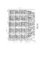
第1圖為一種發光基板的平面示意圖。如第1圖所示,在發光基板01中,多個發光單元002設置在襯底基板001上。例如,每個發光單元002包括驅動電路和多個發光元件。為了使發光元件發光,需要向每個發光單元002的第一電壓端003提供第一電壓信號,並且向每個發光單元002的第二電壓端004提供第二電壓信號。例如,第一電壓信號和第二電壓信號分別為驅動電壓信號和公共電壓信號,或者,第一電壓信號和第二電壓信號分別為公共電壓信號和驅動電壓信號。FIG. 1 is a schematic plan view of a light-emitting substrate. As shown in FIG. 1 , in a light-emitting
多條第一電壓線005和多條第二電壓線006沿行方向延伸,用於分別提供第一電壓信號和第二電壓信號。每個發光單元002的第一電壓端003與第一電壓線005電連接,每個發光單元002的第二電壓端004與第二電壓線006電連接。在發光基板01的邊緣設置有多個綁定管腳007,第一電壓線005和第二電壓線006需要與不同的綁定管腳007電連接,以便於接收與綁定管腳007綁定的控制電路或晶片所提供的驅動電壓信號和公共電壓信號。A plurality of
由於每個綁定管腳007的寬度與第一電壓線005和第二電壓線006的寬度不屬於同一個尺寸量級,且多個綁定管腳007中相鄰兩個綁定管腳007之間的間距更小,而第一電壓線005和第二電壓線006分別需要同時與各個發光單元002和綁定管腳007電連接,因此,第一電壓線005和第二電壓線006無法完全呈直線狀延伸。也即是,如第1圖所示,第一電壓線005包括第一部分005a和第二部分005b。第一部分005a沿行方向延伸,且從第一列發光單元002延伸至最後一列發光單元002。第二部分005b為斜向走線,且從最後一列發光單元002的外側一直延伸至襯底基板001邊緣處的綁定管腳007。類似地,第二電壓線006包括第一部分006a和第二部分006b。第一部分006a沿行方向延伸,且從第一列發光單元002延伸至最後一列發光單元002。第二部分006b為斜向走線,且從最後一列發光單元002的外側一直延伸至襯底基板001邊緣處的綁定管腳007。Since the width of each
依據上述設計準則,發光基板01中需要留出斜向走線區域008,則發光基板01的非顯示區(例如第1圖中下方的邊框)的寬度L1較大,不利於實現窄邊框設計。According to the above design criteria, the
本公開至少一個實施例提供一種發光基板及顯示裝置。該發光基板可以有效減小非顯示區寬度,減小非顯示區的尺寸,有利於實現窄邊框設計。At least one embodiment of the present disclosure provides a light-emitting substrate and a display device. The light-emitting substrate can effectively reduce the width of the non-display area and the size of the non-display area, which is beneficial to realize the design of narrow frame.
下面,將參考附圖詳細地說明本公開的實施例。應當注意的是,不同的附圖中相同的附圖標記將用於指代已描述的相同的元件。Hereinafter, embodiments of the present disclosure will be described in detail with reference to the accompanying drawings. It should be noted that the same reference numerals will be used in different drawings to refer to the same elements that have been described.
本公開至少一個實施例提供一種發光基板,該發光基板包括多個發光單元、多條第一電壓線和多條第一傳輸線。多個發光單元沿第一方向和第二方向排列為N列M行的N*M陣列,第一方向與第二方向交叉,多個發光單元每個包括第一電壓端。多條第一電壓線與多行發光單元一一對應,且配置為傳輸第一電壓信號。第一電壓線包括依序連接的第一部分、第一連接部和第二部分。第一部分沿第二方向延伸,且與對應行的第1列發光單元至第Y列發光單元的第一電壓端電連接。多條第一電壓線中至少一條第一電壓線的第二部分的延伸方向與第一方向和第二方向均具有夾角。第一連接部位於第Y列發光單元與第Y+1列發光單元的交界處,且配置為使第一部分與第二部分電連接。多條第一傳輸線與多行發光單元一一對應,第一傳輸線與對應行的第Y+1列發光單元至第N列發光單元的第一電壓端電連接,以及與對應行的發光單元對應的第一電壓線的第一連接部電連接。N為大於0的整數,M為大於0的整數,0<Y<N且Y為整數。At least one embodiment of the present disclosure provides a light-emitting substrate including a plurality of light-emitting units, a plurality of first voltage lines, and a plurality of first transmission lines. The plurality of light emitting units are arranged in an N*M array of N columns and M rows along the first direction and the second direction, the first direction and the second direction intersect, and each of the plurality of light emitting units includes a first voltage terminal. The plurality of first voltage lines are in one-to-one correspondence with the plurality of rows of light-emitting units, and are configured to transmit first voltage signals. The first voltage line includes a first portion, a first connection portion, and a second portion connected in sequence. The first portion extends along the second direction and is electrically connected to the first voltage terminals of the light-emitting units in the first column to the Y-th column in the corresponding row. The extension direction of the second portion of at least one of the plurality of first voltage lines has an included angle with both the first direction and the second direction. The first connection part is located at the junction of the light-emitting unit in the Y-th column and the light-emitting unit in the Y+1-th column, and is configured to electrically connect the first part and the second part. The plurality of first transmission lines are in one-to-one correspondence with the plurality of rows of light-emitting units, the first transmission lines are electrically connected to the first voltage terminals of the light-emitting units in the Y+1th column to the Nth column of light-emitting units in the corresponding row, and correspond to the light-emitting units in the corresponding row The first connection portion of the first voltage line is electrically connected. N is an integer greater than 0, M is an integer greater than 0, 0<Y<N and Y is an integer.
第2圖為本公開一些實施例提供的一種發光基板的平面示意圖,第3圖為第2圖所示的發光基板的發光單元的排列示意圖。如第2圖和第3圖所示,發光基板10包括襯底基板101和在襯底基板101上陣列排列的多個發光單元100,以及還包括設置在襯底基板101上的多條第一電壓線21和多條第一傳輸線22。FIG. 2 is a schematic plan view of a light-emitting substrate according to some embodiments of the present disclosure, and FIG. 3 is a schematic diagram of the arrangement of light-emitting units of the light-emitting substrate shown in FIG. 2 . As shown in FIGS. 2 and 3 , the light-emitting
例如,多個發光單元100沿第一方向和第二方向排列為N列M行的N*M陣列,N為大於0的整數,M為大於0的整數。例如,第一方向與第二方向交叉。例如,在一些示例中,每一列發光單元100沿第一方向排列,每一行發光單元100沿第二方向排列,第一方向與第二方向垂直,第一方向為列方向,第二方向為行方向。當然,本公開的實施例不限於此,第一方向和第二方向可以為任意的方向,只需使第一方向和第二方向交叉即可。For example, the plurality of light emitting
例如,多個發光單元100不限於沿直線排列,也可以沿曲線排列、沿環形排列或按照任意的方式排列,這可以根據實際需求而定,本公開的實施例對此不作限制。例如,發光單元100的數量可以根據實際需求而定,例如根據發光基板10的尺寸和所需要的亮度而定,雖然第2圖中示出了4列5行發光單元100,但是應當理解,發光單元100的數量不限於此。例如,襯底基板101可以為塑膠基板、矽基板、陶瓷基板、玻璃基板、石英基板等,襯底基板101中包括有單層或多層線路,本公開的實施例對此不作限制。For example, the plurality of light emitting
第4圖為第2圖所示的發光基板的一個發光單元的示意圖。例如,如第4圖所示,對於多個發光單元100,每個發光單元100均包括驅動電路110、多個發光元件120、第一電壓端31和第二電壓端32。FIG. 4 is a schematic diagram of one light-emitting unit of the light-emitting substrate shown in FIG. 2 . For example, as shown in FIG. 4 , for a plurality of light emitting
驅動電路110包括第一輸入端Di、第二輸入端Pwr、輸出端OT和公共電壓端GND。第一輸入端Di接收第一輸入信號,該第一輸入信號例如為位址信號,以用於選通相應位址的驅動電路110。例如,不同的驅動電路110的位址可以相同或不同。第一輸入信號可以為8bit的位址信號,透過解析該位址信號可以獲知待傳輸的位址。第二輸入端Pwr接收第二輸入信號,第二輸入信號例如為電力線載波通信信號。例如,第二輸入信號不僅為驅動電路110提供電能,還向驅動電路110傳輸通信資料,該通信資料可用於控制相應的發光單元100的發光時間,進而控制其視覺上的發光亮度。輸出端OT可在不同的時段內分別輸出不同的信號,例如分別輸出中繼信號和驅動信號。例如,中繼信號為提供給其他驅動電路110的位址信號,也即是,其他驅動電路110的第一輸入端Di接收該中繼信號以作為第一輸入信號,從而獲取位址信號。例如,驅動信號可以為驅動電流,用於驅動發光元件120發光。公共電壓端GND接收公共電壓信號,例如接地信號。例如,公共電壓端GND與第二電壓端32電連接。The driving
驅動電路110配置為根據第一輸入端Di接收的第一輸入信號和第二輸入端Pwr接收的第二輸入信號在第一時段內透過輸出端OT輸出中繼信號,以及在第二時段內透過輸出端OT提供驅動信號至依次串聯的多個發光元件120。在第一時段內,輸出端OT輸出中繼信號,該中繼信號被提供給其他驅動電路110以使其他驅動電路110獲得位址信號。在第二時段內,輸出端OT輸出驅動信號,該驅動信號被提供給依次串聯的多個發光元件120,使得發光元件120在第二時段內發光。The driving
例如,第一時段與第二時段為不同的時段,第一時段例如可以早於第二時段。第一時段可以與第二時段連續相接,第一時段的結束時刻即為第二時段的開始時刻;或者,第一時段與第二時段中間還可以有其他時段,該其他時段可以用於實現其他需要的功能,該其他時段也可以僅用於使第一時段和第二時段間隔開,以避免輸出端OT在第一時段和第二時段的信號彼此干擾。For example, the first time period and the second time period are different time periods, and the first time period may be earlier than the second time period, for example. The first time period can be continuously connected with the second time period, and the end time of the first time period is the start time of the second time period; For other required functions, the other period can also be used only to separate the first period and the second period, so as to prevent the signals of the output terminal OT from interfering with each other in the first period and the second period.
例如,多個發光元件120依次串聯,並且連接在第一電壓端31和輸出端OT之間。例如,多個發光元件120可以包括多個微型發光二極體(Micro-LED)或多個迷你發光二極體(Mini-LED),也即是,任意一個發光元件120可以為Micro-LED或Mini-LED。例如,每個發光元件120包括正極(+)和負極(-)(或者,也可稱為陽極和陰極),多個發光元件120的正極和負極依序首尾串聯,從而在第一電壓端31和輸出端OT之間形成電流路徑。第一電壓端31提供驅動電壓信號,例如在需要使發光元件120發光的時段(第二時段)內為高電壓,而在其他時段內為低電壓。由此,在第二時段內,驅動電壓信號(例如驅動電流)從第一電壓端31依次流經多個發光元件120,然後流入驅動電路110的輸出端OT。多個發光元件120在驅動電流流過時發光,透過控制驅動電流的持續時間,可以控制發光元件120的發光時間,從而控制視覺上的發光亮度。For example, a plurality of
例如,如第4圖所示,在一些示例中,一個發光單元100包括6個發光元件120,該6個發光元件120排列為2列3行。例如,按照從左至右、從上至下的方式給該6個發光元件120依次編號為(1, 1)、(1, 2)、(1, 3)、(2, 1)、(2, 2)和(2, 3),編號在第4圖中示出。例如,將6個發光元件120串聯時,以位置(2, 1)處的發光元件120作為串聯的起點,依次連接(1, 1)、(2, 2)、(1, 2)、(2, 3)和(1, 3)位置處的發光元件120,以位置(1, 3)處的發光元件120作為串聯的終點。例如,位置(2, 1)處的發光元件120的正極連接第一電壓端31,位置(1, 3)處的發光元件120的負極連接驅動電路110的輸出端OT。採用這種分佈方式和串聯方式,可以有效避免走線交疊,便於設計和製備,並且,串聯線路上任意的相鄰兩個發光元件120之間的走線的彎折形狀和長度大致相同,使得線路本身的電阻較為均衡,可以提高負載均衡性,提高電路的穩定性。For example, as shown in FIG. 4, in some examples, one light-emitting
例如,在同一個發光單元100中,多個(例如6個)發光元件120陣列排列,可以使發光更為均勻。驅動電路110位於多個發光元件120構成的陣列的空隙中。For example, in the same light-emitting
需要說明的是,本公開的實施例中,每個發光單元100中的發光元件120的數量不受限制,可以為4個、5個、7個、8個等任意數量,而不限於6個。多個發光元件120可以採用任意的排列方式,例如按照所需要的圖案排列,而不限於矩陣排列方式。驅動電路110的設置位置不受限制,可以設置在發光元件120彼此之間的任意空隙中,這可以根據實際需求而定,本公開的實施例對此不作限制。It should be noted that, in the embodiments of the present disclosure, the number of light-emitting
需要說明的是,第一電壓端31可以接收驅動電壓信號並將該驅動電壓信號提供給發光元件120,也可以接受公共電壓信號並將該公共電壓信號提供給發光元件120,這可以根據驅動電路110的實際工作方式和多個發光元件120的串聯方式而定,本公開的實施例對此不作限制。例如,驅動電壓信號的電位大於公共電壓信號的電位,公共電壓信號例如為接地信號。It should be noted that the
需要說明的是,第4圖所示的發光單元100的構成方式僅為一個示例,不應理解為對本公開實施例的限制。例如,在其他一些示例中,發光單元100可以僅包括發光元件120,而不再需要設置驅動電路110,這該情形下,可以採用被動矩陣(Passive Matrix,PM)驅動方式來驅動各個發光元件120。例如,在再一些示例中,也可以在發光單元100中設置包含薄膜電晶體(Thin Film Transistor,TFT)的電路,採用主動矩陣(Active Matrix,AM)驅動方式,利用該電路對發光元件120進行主動驅動,該電路例如為通常的畫素電路且還可以包括電容等器件,在該情形下,可以省略前述的驅動電路110。發光單元100還可以採用其他任意適用的構成方式,本公開的實施例對此不作限制。It should be noted that the structure of the light-emitting
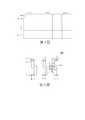
第5A圖為第2圖所示的發光基板的第一電壓線和第二電壓線的放大示意圖,第5B圖為第2圖所示的發光基板中位於最後一列的一個發光單元與第一電壓線和第二電壓線的連接關係示意圖。FIG. 5A is an enlarged schematic view of the first voltage line and the second voltage line of the light-emitting substrate shown in FIG. 2 , and FIG. 5B is a light-emitting unit located in the last column of the light-emitting substrate shown in FIG. 2 and the first voltage Schematic diagram of the connection relationship between the line and the second voltage line.
例如,如第2圖、第5A圖和第5B圖所示,多條第一電壓線21與多行發光單元100一一對應,且配置為傳輸第一電壓信號。例如,該第一電壓信號為驅動電壓信號或公共電壓信號。第一電壓線21包括依序連接的第一部分211、第一連接部213和第二部分212。例如,對於同一條第一電壓線21,第一部分211沿第一方向的寬度大於第二部分212沿第一方向的寬度。例如,對於同一條第一電壓線21,第一部分211在不同位置處沿第一方向的寬度可以相等,第二部分212在不同位置處沿第一方向的寬度可以不同。例如,從與第一連接部213相接的一端到與綁定管腳41(將在後文描述)相接的一端,第二部分212沿第一方向的寬度例如逐漸減小,也即是,第二部分212逐漸收窄,從而滿足佈線設計需求。For example, as shown in FIG. 2 , FIG. 5A and FIG. 5B , the plurality of
例如,第一部分211沿第二方向延伸,且與對應行的第1列發光單元100至第Y列發光單元100的第一電壓端31電連接,例如透過過孔實現電連接。在第2圖的示例中,第一部分211與對應行的第1列發光單元100至第3列發光單元100的第一電壓端31電連接。For example, the
需要說明的是,第2圖中的第一電壓線21所在的膜層位於發光元件120更靠近襯底基板101的一側,因此,第一電壓線21的第一部分211可以延伸至發光單元100中靠近第一電壓端31的發光元件120的正極下方並透過過孔與該發光元件120的正極電連接(也即與第一電壓端31電連接),也即是,第一電壓線21將第一電壓信號傳輸至該發光元件120的正極(也即傳輸至第一電壓端31)。雖然第2圖中發光元件120的負極與第一電壓線21交疊,但是由於兩者位於不同的膜層,因此發光元件120的負極不與第一電壓線21電連接。It should be noted that the film layer where the
多條第一電壓線21中至少一條第一電壓線21的第二部分212的延伸方向與第一方向和第二方向均具有夾角。例如,該夾角可以大於0度且小於90度(例如20~70度,40~60度,或者45度),該延伸方向與第一方向的夾角和該延伸方向與第二方向的夾角可以相同或不同。例如,在第2圖的示例中,至少一條第一電壓線21的第二部分212斜向延伸,也即,與列方向和行方向均具有夾角。需要說明的是,可以一些第一電壓線21的第二部分212斜向延伸,也可以全部第一電壓線21的第二部分212均斜向延伸,這可以根據實際佈線需求而定,本公開的實施例對此不作限制。The extending direction of the
第一連接部213位於第Y列發光單元100與第Y+1列發光單元100的交界處,且配置為使第一部分211與第二部分212電連接,0<Y<N且Y為整數。例如,在第2圖的示例中,第一連接部213位於第3列發光單元100與第4列發光單元100的交界處,此時Y=3,N=4,Y=N-1。例如,第一連接部213實際上為第一電壓線21的彎折部分,以使第一電壓線21的延伸方向改變。需要說明的是,第一連接部213涵蓋的區域不受限制,第一連接部213可以不僅包括第一電壓線21的彎折部分,還可以包括第一電壓線21沿第二方向延伸的線段中的一部分,還可以包括第一電壓線21斜向延伸的線段中的一部分,本公開的實施例對此不作限制。The
多條第一傳輸線22與多行發光單元100一一對應。第一傳輸線22與對應行的第Y+1列發光單元100至第N列發光單元100的第一電壓端31電連接,以及與對應行的發光單元100對應的第一電壓線21的第一連接部213電連接。例如,在第2圖的示例中,第一傳輸線22與對應行的第4列發光單元100的第一電壓端31電連接,以及與對應行的發光單元100對應的第一電壓線21的第一連接部213電連接,由此使得第4列發光單元100的第一電壓端31與第一電壓線21實現電連接,從而可以接收第一電壓線21提供的第一電壓信號。此時,Y=3,N=4,Y=N-1。The plurality of
例如,第一電壓線21與第一傳輸線22位於不同層,由此可以方便佈線。例如,可以透過過孔實現第一電壓線21與第一傳輸線22的電連接。當然,本公開的實施例不限於此,第一電壓線21與第一傳輸線22也可以位於同一層,只要能實現相應的電連接且不會與其他結構短路即可。例如,第一電壓線21的第一部分211在第一方向上的寬度大於第一傳輸線22在第一方向上的寬度。For example, the
需要說明的是,在本公開的說明中,位於“不同層”是指位於不同的膜層,這些不同的膜層在未設置過孔的位置處彼此絕緣。例如,當需要使位於不同的膜層中的走線(例如第一電壓線21和第一傳輸線22)彼此電連接時,可以透過設置過孔的方式使位於不同的膜層中的走線實現電連接。例如,這些不同的膜層是在不同的程序中製備的,例如先採用第一程序製備這些不同的膜層中的一個膜層,然後再採用第二程序製備這些不同的膜層中的另一個膜層。例如,在實施第一程序之後且實施第二程序之前,還可以採用第三程序製備絕緣層,該絕緣層位於不同的膜層之間,以使不同的膜層在未設置過孔的位置處彼此絕緣。例如,第一程序、第二程序和第三程序可以相同或不同。例如,在垂直於襯底基板101的方向上,不同的膜層距襯底基板101的距離不同。也即是,在不同的膜層中,一個膜層距襯底基板101較近,而另一個膜層距襯底基板101較遠。在後文的說明中,位於“不同層”的含義可參考上文描述,不再贅述。It should be noted that, in the description of the present disclosure, being located in "different layers" refers to being located in different film layers, and these different film layers are insulated from each other at the positions where the via holes are not provided. For example, when it is necessary to electrically connect the traces located in different film layers (for example, the
需要說明的是,在本公開的說明中,位於“同一層”是指位於同一個膜層。例如,位於同一個膜層中的走線可以在同一個程序中製備,例如透過一次圖案化程序形成所需要的走線。例如,在垂直於襯底基板101的方向上,位於同一個膜層中的走線距襯底基板101的距離相同或基本相同。也即是,該膜層中的走線距離襯底基板101的遠近程度相同或基本相同。在後文的說明中,位於“同一層”的含義可參考上文描述,不再贅述。It should be noted that, in the description of the present disclosure, being in the "same layer" means being in the same film layer. For example, traces in the same film layer can be prepared in the same process, eg, through a patterning process to form the desired traces. For example, in a direction perpendicular to the
在第2圖所示的示例中,由於第一電壓線21的第一部分211沿第二方向(也即行方向)延伸,位於同一行的第1列發光單元100至第3列發光單元100的第一電壓端31位於第一電壓線21在襯底基板101上的正投影內(例如位於第一部分211在襯底基板101上的正投影內),因此,對於第1列發光單元100至第3列發光單元100,可以透過在第一電壓端31的位置設置過孔以實現第一電壓端31與第一電壓線21的電連接。第一電壓線21的第二部分212斜向延伸,第4列發光單元100的第一電壓端31位於第一電壓線21在襯底基板101上的正投影之外(例如位於第二部分212在襯底基板101上的正投影之外),因此,對於第4列發光單元100,無法透過在第一電壓端31的位置設置過孔來實現第一電壓端31與第一電壓線21的電連接,而是需要透過設置第一傳輸線22來使第一電壓端31與第一電壓線21電連接。In the example shown in FIG. 2 , since the
透過使第一電壓線21從距離發光基板10的邊緣(例如第2圖所示的發光基板10的下邊緣)較遠的位置開始斜向延伸並逐漸收窄,既保證了各列發光單元100中的第一電壓端31與第一電壓線21之間的電連接,又可以有效縮小斜向走線區域,減小發光基板10的邊框,使得非顯示區寬度L2較小,有助於減小發光基板10的非顯示區的尺寸,有利於實現窄邊框設計。By making the
需要說明的是,在該示例中,第一傳輸線22沿第二方向延伸至第一連接部213,並透過過孔與第一連接部213電連接,從而便於第一傳輸線22的佈線,有利於簡化版圖設計。但是,本公開的實施例不限於此,第一傳輸線22也可以沿任意的方向延伸並且與第一電壓線21的任意部分(例如第一部分211或第二部分212)實現電連接,這可以根據實際需求而定,例如根據實際佈線設計而定,本公開的實施例對此不作限制。It should be noted that, in this example, the
例如,如第2圖、第5A圖和第5B圖所示,該發光基板10還包括多條第二電壓線23和多條第二傳輸線24。多條第二電壓線23與多行發光單元100一一對應,且配置為傳輸第二電壓信號。例如,該第二電壓信號為公共電壓信號或驅動電壓信號。需要說明的是,若前述的第一電壓信號為驅動電壓信號,則該第二電壓信號為公共電壓信號,且第一電壓信號的電位大於第二電壓信號的電位;若前述的第一電壓信號為公共電壓信號,則該第二電壓信號為驅動電壓信號,且第一電壓信號的電位小於第二電壓信號的電位。例如,公共電壓信號為接地信號。第一電壓信號和第二電壓信號的具體電位和信號類型可以根據實際需求而定,例如根據發光單元100的結構形式和工作方式而定,本公開的實施例對此不作限制。For example, as shown in FIG. 2 , FIG. 5A and FIG. 5B , the light-emitting
例如,第二電壓線23包括依序連接的第三部分231、第二連接部233和第四部分232。例如,對於同一條第二電壓線23,第三部分231沿第一方向的寬度大於第四部分232沿第一方向的寬度。例如,對於同一條第二電壓線23,第三部分231在不同位置處沿第一方向的寬度可以相等,第四部分232在不同位置處沿第一方向的寬度可以不同。例如,從與第二連接部233相接的一端到與綁定管腳41(將在後文描述)相接的一端,第四部分232沿第一方向的寬度例如逐漸減小,也即是,第四部分232逐漸收窄,從而滿足佈線設計需求。For example, the
例如,第三部分231沿第二方向延伸,且與對應行的第1列發光單元100至第Y列發光單元100的第二電壓端32電連接,例如透過過孔實現電連接。在第2圖的示例中,第三部分231與對應行的第1列發光單元100至第3列發光單元100的第二電壓端32電連接。For example, the
需要說明的是,第2圖中的第二電壓線23所在的膜層位於驅動電路110更靠近襯底基板101的一側,因此,第二電壓線23的第三部分231可以延伸至驅動電路110的公共電壓端GND下方並透過過孔與該驅動電路110的公共電壓端GND電連接(也即與第二電壓端32電連接),也即是,第二電壓線23將第二電壓信號傳輸至該驅動電路110的公共電壓端GND(也即傳輸至第二電壓端32)。雖然第2圖中驅動電路110的其他埠以及發光元件120與第二電壓線23交疊,但是由於第二電壓線23位於與驅動電路110和發光元件120所在的膜層不同的膜層,因此驅動電路110的其他埠和發光元件120不與第二電壓線23電連接。It should be noted that the film layer where the
多條第二電壓線23中至少一條第二電壓線23的第四部分232的延伸方向與第一方向和第二方向均具有夾角。例如,該夾角可以大於0度且小於90度(例如20~70度,40~60度,或者45度),該延伸方向與第一方向的夾角和該延伸方向與第二方向的夾角可以相同或不同。例如,在第2圖的示例中,至少一條第二電壓線23的第四部分232斜向延伸,也即,與列方向和行方向均具有夾角。需要說明的是,可以一些第二電壓線23的第四部分232斜向延伸,也可以全部第二電壓線23的第四部分232均斜向延伸,這可以根據實際佈線需求而定,本公開的實施例對此不作限制。The extending direction of the
第二連接部233位於第Y列發光單元100與第Y+1列發光單元100的交界處,且配置為使第三部分231與第四部分232電連接,0<Y<N且Y為整數。例如,在第2圖的示例中,第二連接部233位於第3列發光單元100與第4列發光單元100的交界處,此時Y=3,N=4,Y=N-1。例如,第二連接部233實際上為第二電壓線23的彎折部分,以使第二電壓線23的延伸方向改變。需要說明的是,第二連接部233涵蓋的區域不受限制,第二連接部233可以不僅包括第二電壓線23的彎折部分,還可以包括第二電壓線23沿第二方向延伸的線段中的一部分,還可以包括第二電壓線23斜向延伸的線段中的一部分,本公開的實施例對此不作限制。The
多條第二傳輸線24與多行發光單元100一一對應。第二傳輸線24與對應行的第Y+1列發光單元100至第N列發光單元100的第二電壓端32電連接,以及與對應行的發光單元100對應的第二電壓線23的第二連接部233電連接。例如,在第2圖的示例中,第二傳輸線24與對應行的第4列發光單元100的第二電壓端32電連接,以及與對應行的發光單元100對應的第二電壓線23的第二連接部233電連接,由此使得第4列發光單元100的第二電壓端32與第二電壓線23實現電連接,從而可以接收第二電壓線23提供的第二電壓信號。此時,Y=3,N=4,Y=N-1。The plurality of
例如,第二電壓線23與第二傳輸線24位於不同層,由此可以方便佈線。例如,可以透過過孔實現第二電壓線23與第二傳輸線24的電連接。當然,本公開的實施例不限於此,第二電壓線23與第二傳輸線24也可以位於同一層,只要能實現相應的電連接且不會與其他結構短路即可。例如,第二電壓線23的第四部分232在第一方向上的寬度大於第二傳輸線24在第一方向上的寬度。For example, the
例如,第一電壓線21和第二電壓線23可以位於同一層,第一傳輸線22和第二傳輸線24可以位於同一層,第一電壓線21與第一傳輸線22位於不同層。由此,可以利用兩個膜層來設置第一電壓線21、第二電壓線23、第一傳輸線22和第二傳輸線24,第一電壓線21和第二電壓線23位於其中一個膜層,第一傳輸線22和第二傳輸線24位於其中另一個膜層,從而可以簡化程序,且避免短路。For example, the
在第2圖所示的示例中,由於第二電壓線23的第三部分231沿第二方向(也即行方向)延伸,位於同一行的第1列發光單元100至第3列發光單元100的第二電壓端32位於第二電壓線23在襯底基板101上的正投影內(例如位於第三部分231在襯底基板101上的正投影內),因此,對於第1列發光單元100至第3列發光單元100,可以透過在第二電壓端32的位置設置過孔以實現第二電壓端32與第二電壓線23的電連接。第二電壓線23的第四部分232斜向延伸,第4列發光單元100的第二電壓端32位於第二電壓線23在襯底基板101上的正投影之外(例如位於第四部分232在襯底基板101上的正投影之外),因此,對於第4列發光單元100,無法透過在第二電壓端32的位置設置過孔來實現第二電壓端32與第二電壓線23的電連接,而是需要透過設置第二傳輸線24來使第二電壓端32與第二電壓線23電連接。In the example shown in FIG. 2 , since the
透過使第二電壓線23從距離發光基板10的邊緣(例如第2圖所示的發光基板10的下邊緣)較遠的位置開始斜向延伸並逐漸收窄,既保證了各列發光單元100中的第二電壓端32與第二電壓線23之間的電連接,又可以有效縮小斜向走線區域,減小發光基板10的邊框,使得非顯示區寬度L2較小,有助於減小發光基板10的非顯示區的尺寸,有利於實現窄邊框設計。By making the
需要說明的是,在該示例中,第二傳輸線24沿第二方向延伸至第二連接部233,並透過過孔與第二連接部233電連接,從而便於第二傳輸線24的佈線,有利於簡化版圖設計。但是,本公開的實施例不限於此,第二傳輸線24也可以沿任意的方向延伸並且與第二電壓線23的任意部分(例如第三部分231或第四部分232)實現電連接,這可以根據實際需求而定,例如根據實際佈線設計而定,本公開的實施例對此不作限制。It should be noted that, in this example, the
需要說明的是,本公開的實施例中,Y可以等於N-1,也可以等於N-2,還可以為其他數值,本公開的實施例對此不作限制。當Y=N-1時,第一電壓線21和第二電壓線23從最後一列發光單元100與倒數第二列發光單元100的交界處開始斜向延伸。當Y=N-2時,第一電壓線21和第二電壓線23從倒數第二列發光單元100與倒數第三列發光單元100的交界處開始斜向延伸。當Y等於其他數值時,第一電壓線21和第二電壓線23可以從更遠離發光基板10的邊緣(例如第2圖中所示的發光基板10的下邊緣)的位置開始斜向延伸。由此,可以根據發光基板10的實際佈線需求調節第一電壓線21和第二電壓線23的延伸方式,以實現窄邊框設計。It should be noted that, in the embodiments of the present disclosure, Y may be equal to N-1, may also be equal to N-2, or may be other numerical values, which are not limited in the embodiments of the present disclosure. When Y=N-1, the
需要說明的是,本公開的實施例中,可以僅第一電壓線21採用上述佈線方式(即從第Y列發光單元100與第Y+1列發光單元100的交界處開始斜向延伸),也可以僅第二電壓線23採用上述佈線方式(即從第Y列發光單元100與第Y+1列發光單元100的交界處開始斜向延伸),還可以第一電壓線21和第二電壓線23均採用上述佈線方式,本公開的實施例對此不作限制。例如,當第一電壓線21和第二電壓線23均採用上述佈線方式時,第一電壓線21開始斜向延伸的位置與第二電壓線23開始斜向延伸的位置可以相同或不同,也即,對應於第一電壓線21的Y值與對應於第二電壓線23的Y值可以相同或不同,本公開的實施例對此不作限制。It should be noted that, in the embodiment of the present disclosure, only the
需要說明的是,在第2圖所示的發光基板10中,第一電壓線21沿第一方向的寬度與第二電壓線23沿第一方向的寬度不同,第一電壓線21更窄,而第二電壓線23更寬,這僅是為了在第2圖中更清晰地區分第一電壓線21和第二電壓線23,而不應理解為對本公開實施例的限制。第一電壓線21與第二電壓線23可以具有相同或基本相同的寬度,第一電壓線21的寬度也可以大於或小於第二電壓線23的寬度,這可以根據實際需求而定,本公開的實施例對此不作限制。It should be noted that, in the light-emitting
需要說明的是,本公開的實施例中,多條第一傳輸線22中至少一條第一傳輸線22沿第二方向延伸,也即是,可以僅一條第一傳輸線22沿第二方向延伸,也可以一些第一傳輸線22沿第二方向延伸,還可以全部第一傳輸線22沿第二方向延伸,這可以根據實際佈線需求而定,本公開的實施例對此不作限制。類似地,多條第二傳輸線24中至少一條第二傳輸線24沿第二方向延伸,也即是,可以僅一條第二傳輸線24沿第二方向延伸,也可以一些第二傳輸線24沿第二方向延伸,還可以全部第二傳輸線24沿第二方向延伸,這可以根據實際佈線需求而定,本公開的實施例對此不作限制。透過使第一傳輸線22和第二傳輸線24沿第二方向延伸,可以縮短第一傳輸線22和第二傳輸線24的長度,從而減小傳輸電阻。It should be noted that, in the embodiment of the present disclosure, at least one
例如,如第2圖所示,發光基板10還包括綁定區BR,該綁定區BR位於發光基板10靠近第N列發光單元100的邊緣,例如,第2圖所示的發光基板10的下邊緣。綁定區BR包括多個綁定管腳41,第一電壓線21的第二部分212與多個綁定管腳41至少之一電連接,第二電壓線23的第四部分232與多個綁定管腳41至少之一電連接。例如,每條第一電壓線21的第二部分212可以與一個或多個綁定管腳41電連接,類似地,每條第二電壓線23的第四部分232也可以與一個或多個綁定管腳41電連接。同一條第一電壓線21與多個綁定管腳41電連接或者同一條第二電壓線23與多個綁定管腳41電連接,可以提高連接可靠性,降低傳輸電阻。綁定區BR中的綁定管腳41可以透過柔性電路板與另行設置的控制電路或晶片電連接,從而便於接收該控制電路或晶片傳輸的第一電壓信號和第二電壓信號,並將第一電壓信號和第二電壓信號傳輸至第一電壓線21和第二電壓線23。For example, as shown in FIG. 2 , the light-emitting
例如,如第2圖所示,該發光基板10還包括多條位址轉接線130,多條位址轉接線130沿第一方向延伸且配置為傳輸第一輸入信號。For example, as shown in FIG. 2 , the light-emitting
例如,發光基板10中的多個發光單元100排列為N列M行且劃分為多組,每組發光單元100包括X列M行共X*M個發光單元100,多條位址轉接線130與多組發光單元100一一對應。此時,發光單元100劃分為N/X組。例如,在第2圖所示的示例中,每組發光單元100包括2列5行共10個發光單元100,因此,每2列發光單元100對應一條位址轉接線130,發光基板10中的位址轉接線130的數量為N/2。例如,0<X≤N且X為整數。For example, the plurality of light-emitting
例如,在同一組發光單元100中,X*M個發光單元100根據行列分佈位置依次編號。例如,在一些示例中,如第6A圖所示,X*M個發光單元按照Z形逐列逐行依次編號,第6A圖中每個矩形表示一個發光單元100,各個發光單元100的編號標注在各個矩形中。例如,在另一些示例中,如第6B圖所示,X*M個發光單元按照S形逐列逐行依次編號,類似地,第6B圖中每個矩形表示一個發光單元100,各個發光單元100的編號標注在各個矩形中。需要說明的是,發光單元100根據行列分佈位置依次編號的方式不限於上文描述的方式,也可以根據其他方式進行編號,使得多個發光單元100的連接方式可靈活調節,本公開的實施例對此不作限制。For example, in the same group of light-emitting
例如,如第2圖和第4圖所示,在同一組發光單元100中,編號為1的發光單元100的驅動電路110的第一輸入端Di與該組發光單元100對應的位址轉接線130電連接,編號為P的發光單元100的驅動電路110的輸出端OT與編號為P+1的發光單元100的驅動電路110的第一輸入端Di電連接,編號為P+1的發光單元100的驅動電路110的第一輸入端Di接收編號為P的發光單元100的驅動電路110的輸出端OT輸出的中繼信號以作為第一輸入信號。例如,0<P<X*M且P為整數。For example, as shown in FIGS. 2 and 4, in the same group of light-emitting
例如,當採用第6A圖所示的編號方式時,對於編號為1的一組發光單元100(即發光基板10最上側的一組發光單元100,或者稱為第一組發光單元100),位於第一列第一行的發光單元100的驅動電路110的第一輸入端Di與該組發光單元100對應的位址轉接線130電連接,各個發光單元100的驅動電路110的輸出端OT與後一個發光單元100的驅動電路110的第一輸入端Di電連接(最後一個發光單元100的驅動電路110的輸出端OT不與其他驅動電路110連接)。對於編號為2的一組發光單元100(即緊鄰第一組發光單元100的一組發光單元100,或者稱為第二組發光單元100),位於第三列第一行的發光單元100的驅動電路110的第一輸入端Di與該組發光單元100對應的位址轉接線130電連接,各個發光單元100的驅動電路110的輸出端OT與後一個發光單元100的驅動電路110的第一輸入端Di電連接,其連接方式與第一組發光單元100類似。For example, when the numbering method shown in FIG. 6A is adopted, for a group of light-emitting
透過上述連接方式,在每組發光單元100中,只有第一個發光單元100的驅動電路110的第一輸入端Di與位址轉接線130電連接,而其他發光單元100的驅動電路110的第一輸入端Di接收前一個發光單元100的驅動電路110輸出的中繼信號作為第一輸入信號。由此,對於一組發光單元100,只需要透過一條位址轉接線130提供一個第一輸入信號(即位址信號),便可以使該組發光單元100中的所有發光單元100均獲得各自的位址信號。這樣極大地減少了信號線的數量,節省了佈線空間,並且簡化了控制方式。Through the above connection method, in each group of light-emitting
例如,如第2圖和第4圖所示,該發光基板10還包括多條電壓轉接線140。多條電壓轉接線140沿第一方向延伸且配置為傳輸第二輸入信號,多條電壓轉接線140與N列發光單元100一一對應。例如,每列發光單元100對應一條電壓轉接線140,發光基板10中的電壓轉接線140的數量為N。例如,如第2圖所示,第一列發光單元100、第二列發光單元100、第三列發光單元100、第四列發光單元100分別對應一條電壓轉接線140。For example, as shown in FIG. 2 and FIG. 4 , the light-emitting
例如,對於一列發光單元100,發光單元100中的驅動電路110的第二輸入端Pwr與包括該驅動電路110的發光單元100所在列對應的電壓轉接線140電連接。也即是,一列發光單元10中所有的驅動電路110的第二輸入端Pwr均與該列對應的電壓轉接線140電連接,以接收第二輸入信號。For example, for a column of light-emitting
例如,如第2圖所示,該發光基板10還包括沿第二方向延伸的多條源位址線150和多條源電壓線160。For example, as shown in FIG. 2 , the light-emitting
例如,多條源位址線150與多條位址轉接線130一一對應電連接,且配置為傳輸第一輸入信號。例如,源位址線150的數量與位址轉接線130的數量相等,均等於N/X,也即是,當發光單元100劃分為N/X組時,每組發光單元100對應一條源位址線150和一條位址轉接線130,該源位址線150和位址轉接線130將第一輸入信號傳輸至該組發光單元100中的第一個發光單元100。For example, the plurality of
例如,多條源電壓線160與多組發光單元100一一對應,每條源電壓線160與對應的一組發光單元100對應的多條電壓轉接線140電連接,且配置為傳輸第二輸入信號。例如,源電壓線160的數量為N/X,也即是,當發光單元100劃分為N/X組時,每組發光單元100對應一條源電壓線160,該源電壓線160將第二輸入信號傳輸至與該組發光單元100對應的多條電壓轉接線140,從而為該組發光單元100中的所有發光單元100提供第二輸入信號。例如,對應於同一組發光單元100的源位址線150和源電壓線160相鄰設置,且位於多行發光單元100的空隙中。For example, a plurality of
需要說明的是,在同一組發光單元100中,所有發光單元100的驅動電路110的第二輸入端Pwr與相應的電壓轉接線140電連接,這些電壓轉接線140連接到同一條源電壓線160。由此,對於一組發光單元100,只需要透過一條源電壓線160提供一個第二輸入信號,便可以使該組發光單元100中的所有發光單元100均獲得第二輸入信號。這樣極大地減少了信號線的數量,節省了佈線空間,並且簡化了控制方式。It should be noted that, in the same group of light-emitting
例如,在該發光基板10中,源位址線150的數量和源電壓線160的數量均為N/X。For example, in the light-emitting
例如,在一些示例中,在襯底基板101之上,源位址線150與源電壓線160位於同一層,電壓轉接線140與位址轉接線130位於同一層,源位址線150與位址轉接線130位於不同層。也即是,源位址線150與源電壓線160採用一次圖案化程序(例如光刻程序)製備,電壓轉接線140與位址轉接線130採用另一次圖案化程序製備,源位址線150與源電壓線160所在的膜層和電壓轉接線140與位址轉接線130所在的膜層之間設置有絕緣層,透過貫穿絕緣層的過孔使相應的走線電連接。透過這種方式,可以簡化製備程序,並且能夠相容通常的半導體膜層製備程序,提高生產效率。For example, in some examples, on the
例如,在該發光基板10中,第一電壓線21、第一傳輸線22、第二電壓線23和第二傳輸線24各自所在的膜層與位址轉接線130、電壓轉接線140、源位址線150和源電壓線160各自所在的膜層可以根據實際需求確定,這些膜層可以相同或不同,本公開的實施例對此不作限制。For example, in the light-emitting
第7圖為本公開一些實施例提供的一種發光基板的佈線設計局部示意圖,第7圖例如為第2圖中區域C1的一種佈線設計示意圖。例如,如第7圖所示,第一傳輸線22由多條線段(例如4條線段)依序連接而構成,這些線段中的一部分線段沿第二方向延伸,另一部分線段沿第一方向延伸,從而使發光單元100的第一電壓端31與第一電壓線21的第一連接部213電連接。類似地,第二傳輸線24由多條線段(例如2條線段)依序連接而構成,這些線段中的一部分線段沿第二方向延伸,另一部分線段沿第一方向延伸,從而使發光單元100的第二電壓端32與第二電壓線23的第二連接部233電連接。FIG. 7 is a partial schematic diagram of a wiring design of a light-emitting substrate according to some embodiments of the present disclosure, and FIG. 7 is, for example, a schematic diagram of a wiring design of the region C1 in FIG. 2 . For example, as shown in FIG. 7, the
需要說明的是,在本公開的說明中,第一傳輸線22沿第二方向延伸是指第一傳輸線22的至少部分線段沿第二方向延伸,而並非指第一傳輸線22完全嚴格地沿第二方向延伸。類似地,第二傳輸線24沿第二方向延伸是指第二傳輸線24的至少部分線段沿第二方向延伸,而並非指第二傳輸線24完全嚴格地沿第二方向延伸。It should be noted that, in the description of the present disclosure, the extension of the
例如,如第7圖所示,第一電壓線21的第二部分212從第N-1列發光單元100與第N列發光單元100的交界處開始斜向延伸,第一傳輸線22的一端透過過孔與第一電壓端31電連接,第一傳輸線22的另一端透過過孔與第一電壓線21的第一連接部分213電連接。類似地,第二電壓線23的第四部分232從第N-1列發光單元100與第N列發光單元100的交界處開始斜向延伸,第二傳輸線24的一端透過過孔與第二電壓端32電連接,第二傳輸線24的另一端透過過孔與第二電壓線23的第二連接部分233電連接。For example, as shown in FIG. 7 , the
第8圖為本公開一些實施例提供的另一種發光基板的平面示意圖。例如,在一些示例中,如第8圖所示,該發光基板10還包括沿第一方向延伸的多條第三電壓線25和多條第四電壓線26。該發光基板10的其他結構與第2圖所示的發光基板10基本相同,此處不再贅述。FIG. 8 is a schematic plan view of another light-emitting substrate provided by some embodiments of the present disclosure. For example, in some examples, as shown in FIG. 8 , the
例如,多條第三電壓線25在平行於發光基板10的平面內的正投影與多條第一電壓線21在平行於發光基板10的平面內的正投影交疊,且多條第三電壓線25透過過孔與多條第一電壓線21電連接。例如,多條第四電壓線26在平行於發光基板10的平面內的正投影與多條第二電壓線23在平行於發光基板10的平面內的正投影交疊,且多條第四電壓線26透過過孔與多條第二電壓線23電連接。例如,多條第三電壓線25和多條第四電壓線26位於同一層。For example, the orthographic projections of the plurality of third voltage lines 25 in the plane parallel to the
例如,多條第三電壓線25透過過孔與多條第一電壓線21電連接且形成網格狀走線,多條第四電壓線26透過過孔與多條第二電壓線23電連接且形成網格狀走線,從而可以減小傳輸電阻,提高發光基板10內的電壓一致性。例如,第三電壓線25和第四電壓線26位於同一層,且與位址轉接線130和電壓轉接線140位於同一層。由於第三電壓線25、第四電壓線26、位址轉接線130和電壓轉接線140均沿第一方向延伸,因此四者可以設置在同一層且彼此不會交疊,從而簡化結構,簡化製備程序。例如,第三電壓線25和第四電壓線26所在的膜層與第一電壓線21和第二電壓線23所在的膜層不同。For example, the plurality of third voltage lines 25 are electrically connected to the plurality of
需要說明的是,本公開的實施例中,第一電壓線21、第二電壓線23、第三電壓線25和第四電壓線26的長度和寬度可以設置為任意數值,其長度可以相同或不同,其寬度也可以相同或不同,這可以根據實際需求而定,本公開的實施例對此不作限制。It should be noted that, in the embodiment of the present disclosure, the lengths and widths of the
需要說明的是,本公開的實施例中,發光基板10還可以包括更多的結構和部件,各個結構和部件的設置方式可以根據實際需求而定,從而實現多樣化的功能,本公開的實施例對此不作限制。It should be noted that, in the embodiment of the present disclosure, the light-emitting
本公開至少一個實施例還提供一種顯示裝置,該顯示裝置包括顯示面板和本公開任一實施例提供的發光基板。該顯示裝置可以有效減小非顯示區寬度,減小非顯示區的尺寸,有利於實現窄邊框設計。At least one embodiment of the present disclosure further provides a display device including a display panel and the light-emitting substrate provided in any embodiment of the present disclosure. The display device can effectively reduce the width of the non-display area and the size of the non-display area, which is beneficial to realize the narrow frame design.
第9圖為本公開一些實施例提供的一種顯示裝置的剖面示意圖。例如,如第9圖所示,在一些實施例中,顯示裝置50包括顯示面板510和發光基板520。例如,發光基板520可以為本公開任一實施例提供的發光基板,例如前述的發光基板10。FIG. 9 is a schematic cross-sectional view of a display device according to some embodiments of the present disclosure. For example, as shown in FIG. 9 , in some embodiments, the display device 50 includes a
例如,顯示面板510具有顯示側P1和與顯示側P1相對的非顯示側P2,發光基板520設置在顯示面板510的非顯示側P2以作為背光單元。例如,發光基板520可以作為面光源向顯示面板510提供背光。例如,顯示面板510可以為LCD面板、電子紙顯示面板等,本公開的實施例對此不作限制。For example, the
例如,顯示裝置50可以為LCD裝置、電子紙顯示裝置等,或者也可以為其他具有顯示功能的裝置等,本公開的實施例對此不作限制。例如,顯示裝置50可以為手機、平板電腦、電視機、顯示器、筆記型電腦、數位相框、導航儀、電子書等任何具有顯示功能的產品或部件,本公開的實施例對此不作限制。For example, the display device 50 may be an LCD device, an electronic paper display device, etc., or may also be other devices having a display function, etc., which are not limited in the embodiments of the present disclosure. For example, the display device 50 may be any product or component with a display function, such as a mobile phone, a tablet computer, a television, a monitor, a notebook computer, a digital photo frame, a navigator, an electronic book, etc., which is not limited by the embodiments of the present disclosure.
需要說明的是,本公開實施例提供的發光基板10既可以作為背光單元應用到上述顯示裝置50中,也可以單獨作為具有顯示功能或發光功能的基板使用,本公開的實施例對此不作限制。It should be noted that the light-emitting
關於該顯示裝置50的詳細說明和技術效果可以參考上文中關於發光基板10的描述,此處不再贅述。該顯示裝置50還可以包括更多的元件和結構,這可以根據實際需求而定,本公開的實施例對此不作限制。For the detailed description and technical effects of the display device 50, reference may be made to the above description of the light-emitting
有以下幾點需要說明: (1)本公開實施例附圖只涉及到本公開實施例涉及到的結構,其他結構可參考通常設計。 (2)在不衝突的情況下,本公開的實施例及實施例中的特徵可以相互組合以得到新的實施例。The following points need to be noted: (1) The drawings of the embodiments of the present disclosure only relate to the structures involved in the embodiments of the present disclosure, and other structures may refer to general designs. (2) The embodiments of the present disclosure and the features in the embodiments may be combined with each other to obtain new embodiments without conflict.
以上所述,僅為本公開的具體實施方式,但本公開的保護範圍並不局限於此,本公開的保護範圍應以所述請求項的保護範圍為准。The above descriptions are only specific embodiments of the present disclosure, but the protection scope of the present disclosure is not limited thereto, and the protection scope of the present disclosure should be subject to the protection scope of the claims.
01,10,520:發光基板 002,100:發光單元 003,004,31,32:電壓端 005,006,21,22,25,26:電壓線 007,41:綁定管腳 005a,006a,211:第一部分 005b,006b,212:第二部分 231:第三部分 232:第四部分 001,101:襯底基板 008:走線區域 L1:寬度 C1:區域 L2:非顯示區寬度 BR:綁定區 22,24:傳輸線 110:驅動電路 120:發光元件 130:位址轉接線 140:電壓轉接線 150:源位址線 160:源電壓線 Di,Pwr:輸入端 OT:輸出端 GND:公共電壓端 213,233:連接部 50:顯示裝置 510:顯示面板 P1:顯示側 P2:非顯示側01,10,520: Light-emitting substrate 002,100: Light unit 003,004,31,32:
為了更清楚地說明本公開實施例的技術方案,下面將對實施例的附圖作簡單地介紹,顯而易見地,下面描述中的附圖僅僅涉及本公開的一些實施例,而非對本公開的限制。 第1圖為一種發光基板的平面示意圖; 第2圖為本公開一些實施例提供的一種發光基板的平面示意圖; 第3圖為第2圖所示的發光基板的發光單元的排列示意圖; 第4圖為第2圖所示的發光基板中一個發光單元的示意圖; 第5A圖為第2圖所示的發光基板的第一電壓線和第二電壓線的放大示意圖; 第5B圖為第2圖所示的發光基板中位於最後一列的一個發光單元與第一電壓線和第二電壓線的連接關係示意圖; 第6A圖和第6B圖為本公開一些實施例提供的發光基板的發光單元的編號方式示意圖; 第7圖為本公開一些實施例提供的一種發光基板的佈線設計局部示意圖; 第8圖為本公開一些實施例提供的另一種發光基板的平面示意圖;以及 第9圖為本公開一些實施例提供的一種顯示裝置的剖面示意圖。In order to explain the technical solutions of the embodiments of the present disclosure more clearly, the accompanying drawings of the embodiments will be briefly introduced below. Obviously, the drawings in the following description only relate to some embodiments of the present disclosure, rather than limit the present disclosure. . Figure 1 is a schematic plan view of a light-emitting substrate; FIG. 2 is a schematic plan view of a light-emitting substrate provided by some embodiments of the present disclosure; FIG. 3 is a schematic diagram of the arrangement of light-emitting units of the light-emitting substrate shown in FIG. 2; FIG. 4 is a schematic diagram of a light-emitting unit in the light-emitting substrate shown in FIG. 2; FIG. 5A is an enlarged schematic view of the first voltage line and the second voltage line of the light-emitting substrate shown in FIG. 2; FIG. 5B is a schematic diagram of the connection relationship between a light-emitting unit located in the last column of the light-emitting substrate shown in FIG. 2 and the first voltage line and the second voltage line; FIGS. 6A and 6B are schematic diagrams of numbering methods of light-emitting units of a light-emitting substrate according to some embodiments of the present disclosure; FIG. 7 is a partial schematic diagram of a wiring design of a light-emitting substrate according to some embodiments of the present disclosure; FIG. 8 is a schematic plan view of another light-emitting substrate provided by some embodiments of the present disclosure; and FIG. 9 is a schematic cross-sectional view of a display device according to some embodiments of the present disclosure.
C1:區域 L2:非顯示區寬度 BR:綁定區 10:發光基板 21,23:電壓線 22,24:傳輸線 31,32:電壓端 41:綁定管腳 100:發光單元 101:襯底基板 130:位址轉接線 140:電壓轉接線 150:源位址線 160:源電壓線C1: Area L2: non-display area width BR: binding region 10: Light-emitting
Claims (14)
Translated fromChineseApplications Claiming Priority (2)
| Application Number | Priority Date | Filing Date | Title |
|---|---|---|---|
| CN202010536696.5 | 2020-06-12 | ||
| CN202010536696.5ACN113805378B (en) | 2020-06-12 | 2020-06-12 | Light-emitting substrate and display device |
Publications (2)
| Publication Number | Publication Date |
|---|---|
| TW202147287A TW202147287A (en) | 2021-12-16 |
| TWI751857Btrue TWI751857B (en) | 2022-01-01 |
Family
ID=78845160
Family Applications (1)
| Application Number | Title | Priority Date | Filing Date |
|---|---|---|---|
| TW109145939ATWI751857B (en) | 2020-06-12 | 2020-12-24 | Light-emitting substrate and display device |
Country Status (7)
| Country | Link |
|---|---|
| US (1) | US11791347B2 (en) |
| EP (1) | EP4067983B1 (en) |
| JP (1) | JP7662637B2 (en) |
| KR (2) | KR102833377B1 (en) |
| CN (1) | CN113805378B (en) |
| TW (1) | TWI751857B (en) |
| WO (1) | WO2021249120A1 (en) |
Families Citing this family (8)
| Publication number | Priority date | Publication date | Assignee | Title |
|---|---|---|---|---|
| CN111812888A (en)* | 2020-07-10 | 2020-10-23 | 深圳市华星光电半导体显示技术有限公司 | Mini LED backlight module, preparation method thereof and display panel |
| CN112669761B (en)* | 2020-12-01 | 2023-05-05 | 厦门天马微电子有限公司 | Display panel, manufacturing method thereof, and display device |
| TWI802171B (en)* | 2021-12-23 | 2023-05-11 | 友達光電股份有限公司 | Display device |
| EP4206807B1 (en)* | 2022-01-01 | 2025-08-06 | LG Display Co., Ltd. | Display apparatus having a back-light unit having light-emitting chips |
| WO2023206278A1 (en)* | 2022-04-28 | 2023-11-02 | 京东方科技集团股份有限公司 | Display panel and manufacturing method therefor, and display apparatus |
| CN118865866B (en)* | 2022-06-30 | 2025-10-03 | 上海天马微电子有限公司 | Driver board, display panel, and display device |
| CN115084185B (en)* | 2022-07-15 | 2025-08-22 | Tcl华星光电技术有限公司 | Light-emitting substrate and display device |
| CN117859204A (en)* | 2022-08-09 | 2024-04-09 | 京东方科技集团股份有限公司 | Substrate and electronic device |
Citations (4)
| Publication number | Priority date | Publication date | Assignee | Title |
|---|---|---|---|---|
| TW201715276A (en)* | 2015-10-16 | 2017-05-01 | 群創光電股份有限公司 | Display device |
| TWI642979B (en)* | 2018-05-03 | 2018-12-01 | 達方電子股份有限公司 | Backlight apparatus |
| US10468396B2 (en)* | 2016-12-30 | 2019-11-05 | Lg Display Co., Ltd. | Display device and multi-screen display device using the same |
| TW201944128A (en)* | 2018-04-18 | 2019-11-16 | 友達光電股份有限公司 | Device substrate, display panel and tiled display |
Family Cites Families (27)
| Publication number | Priority date | Publication date | Assignee | Title |
|---|---|---|---|---|
| JP2010060873A (en)* | 2008-09-04 | 2010-03-18 | Sony Corp | Image display device |
| TWI391731B (en) | 2009-04-21 | 2013-04-01 | Wintek Corp | Flat display panel |
| TWI469123B (en)* | 2012-08-09 | 2015-01-11 | Au Optronics Corp | Display panel |
| KR102163358B1 (en) | 2014-07-21 | 2020-10-12 | 엘지디스플레이 주식회사 | Display Device |
| CN104934458A (en) | 2015-06-29 | 2015-09-23 | 合肥京东方光电科技有限公司 | Display substrate, manufacturing method for display substrate and display apparatus |
| US10475876B2 (en)* | 2016-07-26 | 2019-11-12 | X-Celeprint Limited | Devices with a single metal layer |
| KR102687420B1 (en)* | 2016-08-25 | 2024-07-22 | 엘지디스플레이 주식회사 | Display panel and display device |
| CN106444199A (en)* | 2016-12-23 | 2017-02-22 | 厦门天马微电子有限公司 | Array substrate, display panel and display device |
| KR102734610B1 (en) | 2016-12-30 | 2024-11-25 | 엘지디스플레이 주식회사 | Liquid crystal display device |
| CN106873222B (en)* | 2017-04-20 | 2020-08-04 | 武汉华星光电技术有限公司 | Display panel and display of narrow frame |
| US20190157248A1 (en) | 2017-11-20 | 2019-05-23 | Century Micro Display Technology (Shenzhen) Co., Ltd. | Micro led display panel with narrow border |
| CN108287436B (en) | 2018-01-31 | 2021-03-02 | 武汉华星光电技术有限公司 | Backlight module and liquid crystal display device |
| CN108321281A (en) | 2018-03-30 | 2018-07-24 | 南方科技大学 | micro-L ED display panel and micro-L ED display device |
| CN108732837B (en)* | 2018-05-29 | 2019-10-18 | 武汉华星光电技术有限公司 | Tft array substrate and liquid crystal display panel |
| CN110890020B (en)* | 2018-09-09 | 2022-06-28 | 群创光电股份有限公司 | electronic device |
| US11069668B2 (en)* | 2018-09-09 | 2021-07-20 | Innolux Corporation | Electronic device for reducing a border edge of the non-display areas |
| KR102559818B1 (en) | 2018-09-21 | 2023-07-26 | 삼성디스플레이 주식회사 | Method for arranging light emitting device and method for manufacturing display device including the same |
| CN109413233B (en) | 2018-10-29 | 2021-01-15 | 北京小米移动软件有限公司 | terminal |
| TWI682224B (en) | 2018-12-04 | 2020-01-11 | 友達光電股份有限公司 | Light-emitting module, driving chip, and driving method |
| CN109450539B (en) | 2018-12-24 | 2020-07-14 | 厦门天马微电子有限公司 | Mobile terminal and L IFI signal transceiving method of mobile terminal |
| CN109585462B (en) | 2019-01-23 | 2024-12-13 | 京东方科技集团股份有限公司 | Array substrate and manufacturing method thereof, flexible display panel, and spliced screen |
| CN109949711B (en) | 2019-03-29 | 2021-08-31 | 上海天马微电子有限公司 | Display panel, display device and manufacturing method of display panel |
| CN110323257B (en)* | 2019-04-12 | 2021-05-14 | 武汉天马微电子有限公司 | Array substrate, display panel and display device |
| CN110286534A (en)* | 2019-06-19 | 2019-09-27 | 武汉天马微电子有限公司 | Array substrate, display panel and display device thereof |
| CN110265454A (en)* | 2019-06-25 | 2019-09-20 | 上海天马微电子有限公司 | Display panel, manufacturing method thereof and display device |
| CN110503898A (en) | 2019-08-28 | 2019-11-26 | 京东方科技集团股份有限公司 | Micro-light-emitting diode display panel, preparation method, spliced display panel, and device |
| CN111161639B (en)* | 2020-01-03 | 2022-04-19 | 厦门天马微电子有限公司 | Display panel and display device |
- 2020
- 2020-06-12CNCN202010536696.5Apatent/CN113805378B/enactiveActive
- 2020-12-24TWTW109145939Apatent/TWI751857B/enactive
- 2021
- 2021-05-17USUS17/781,850patent/US11791347B2/enactiveActive
- 2021-05-17KRKR1020227017959Apatent/KR102833377B1/enactiveActive
- 2021-05-17JPJP2022533547Apatent/JP7662637B2/enactiveActive
- 2021-05-17WOPCT/CN2021/094028patent/WO2021249120A1/ennot_activeCeased
- 2021-05-17EPEP21823073.8Apatent/EP4067983B1/enactiveActive
- 2021-05-17KRKR1020257021445Apatent/KR20250108747A/enactivePending
Patent Citations (4)
| Publication number | Priority date | Publication date | Assignee | Title |
|---|---|---|---|---|
| TW201715276A (en)* | 2015-10-16 | 2017-05-01 | 群創光電股份有限公司 | Display device |
| US10468396B2 (en)* | 2016-12-30 | 2019-11-05 | Lg Display Co., Ltd. | Display device and multi-screen display device using the same |
| TW201944128A (en)* | 2018-04-18 | 2019-11-16 | 友達光電股份有限公司 | Device substrate, display panel and tiled display |
| TWI642979B (en)* | 2018-05-03 | 2018-12-01 | 達方電子股份有限公司 | Backlight apparatus |
Also Published As
| Publication number | Publication date |
|---|---|
| KR102833377B1 (en) | 2025-07-11 |
| WO2021249120A1 (en) | 2021-12-16 |
| EP4067983B1 (en) | 2025-04-02 |
| US11791347B2 (en) | 2023-10-17 |
| CN113805378B (en) | 2022-07-26 |
| JP2023528706A (en) | 2023-07-06 |
| US20230028746A1 (en) | 2023-01-26 |
| TW202147287A (en) | 2021-12-16 |
| EP4067983A1 (en) | 2022-10-05 |
| KR20250108747A (en) | 2025-07-15 |
| CN113805378A (en) | 2021-12-17 |
| EP4067983A4 (en) | 2023-06-28 |
| KR20230022828A (en) | 2023-02-16 |
| JP7662637B2 (en) | 2025-04-15 |
Similar Documents
| Publication | Publication Date | Title |
|---|---|---|
| TWI751857B (en) | Light-emitting substrate and display device | |
| CN112151696B (en) | Display panel and display device | |
| CN113130463B (en) | A light-emitting substrate, its preparation method, and a display device | |
| CN111128048B (en) | Display panel and display device | |
| TWI767473B (en) | Light-emitting substrate and driving method thereof, and display device | |
| WO2022160203A1 (en) | Driving backplate, display panel, and display device | |
| US20240404959A1 (en) | Wiring substrate, array substrate and light emitting module having control regions arranged into control region rows and control region columns | |
| CN111948859A (en) | Display substrate and display device | |
| CN115938227A (en) | Display panel and display device | |
| WO2022104752A1 (en) | Light-emitting substrate and display device | |
| CN116456771A (en) | Display panel and display device | |
| CN115064121A (en) | Display panel and display device | |
| CN115084185A (en) | Light-emitting substrate and display device | |
| CN114783365A (en) | Display module and display device | |
| CN113498490B (en) | Light-emitting substrate and display device | |
| CN111857448A (en) | Display module and preparation method thereof, and display device | |
| CN116249400A (en) | Display substrate and display device | |
| CN115273735A (en) | Display panel and display device | |
| WO2022266795A9 (en) | Driving backplane and manufacturing method therefor, and display device | |
| CN222721937U (en) | Display substrate, display device | |
| CN115315812B (en) | Display substrate and display device | |
| WO2023077269A1 (en) | Display substrate and display device | |
| WO2022222066A1 (en) | Display substrate, display panel, and display apparatus | |
| CN118076168A (en) | Display panel, display module and display device | |
| CN115132757A (en) | Array substrate, display panel and display device |