TWI750814B - Semiconductor device and manufacturing method thereof - Google Patents
Semiconductor device and manufacturing method thereofDownload PDFInfo
- Publication number
- TWI750814B TWI750814BTW109132407ATW109132407ATWI750814BTW I750814 BTWI750814 BTW I750814BTW 109132407 ATW109132407 ATW 109132407ATW 109132407 ATW109132407 ATW 109132407ATW I750814 BTWI750814 BTW I750814B
- Authority
- TW
- Taiwan
- Prior art keywords
- oxide semiconductor
- layer
- semiconductor layer
- film
- electrode layer
- Prior art date
Links
Images


Classifications
- H—ELECTRICITY
- H10—SEMICONDUCTOR DEVICES; ELECTRIC SOLID-STATE DEVICES NOT OTHERWISE PROVIDED FOR
- H10D—INORGANIC ELECTRIC SEMICONDUCTOR DEVICES
- H10D30/00—Field-effect transistors [FET]
- H10D30/60—Insulated-gate field-effect transistors [IGFET]
- H10D30/67—Thin-film transistors [TFT]
- H10D30/674—Thin-film transistors [TFT] characterised by the active materials
- H10D30/6755—Oxide semiconductors, e.g. zinc oxide, copper aluminium oxide or cadmium stannate
- H—ELECTRICITY
- H01—ELECTRIC ELEMENTS
- H01L—SEMICONDUCTOR DEVICES NOT COVERED BY CLASS H10
- H01L21/00—Processes or apparatus adapted for the manufacture or treatment of semiconductor or solid state devices or of parts thereof
- H01L21/02—Manufacture or treatment of semiconductor devices or of parts thereof
- H01L21/02104—Forming layers
- H01L21/02107—Forming insulating materials on a substrate
- H01L21/02109—Forming insulating materials on a substrate characterised by the type of layer, e.g. type of material, porous/non-porous, pre-cursors, mixtures or laminates
- H01L21/02112—Forming insulating materials on a substrate characterised by the type of layer, e.g. type of material, porous/non-porous, pre-cursors, mixtures or laminates characterised by the material of the layer
- H01L21/02123—Forming insulating materials on a substrate characterised by the type of layer, e.g. type of material, porous/non-porous, pre-cursors, mixtures or laminates characterised by the material of the layer the material containing silicon
- H01L21/02164—Forming insulating materials on a substrate characterised by the type of layer, e.g. type of material, porous/non-porous, pre-cursors, mixtures or laminates characterised by the material of the layer the material containing silicon the material being a silicon oxide, e.g. SiO2
- H—ELECTRICITY
- H01—ELECTRIC ELEMENTS
- H01L—SEMICONDUCTOR DEVICES NOT COVERED BY CLASS H10
- H01L21/00—Processes or apparatus adapted for the manufacture or treatment of semiconductor or solid state devices or of parts thereof
- H01L21/02—Manufacture or treatment of semiconductor devices or of parts thereof
- H01L21/02104—Forming layers
- H01L21/02107—Forming insulating materials on a substrate
- H01L21/02109—Forming insulating materials on a substrate characterised by the type of layer, e.g. type of material, porous/non-porous, pre-cursors, mixtures or laminates
- H01L21/02112—Forming insulating materials on a substrate characterised by the type of layer, e.g. type of material, porous/non-porous, pre-cursors, mixtures or laminates characterised by the material of the layer
- H01L21/02123—Forming insulating materials on a substrate characterised by the type of layer, e.g. type of material, porous/non-porous, pre-cursors, mixtures or laminates characterised by the material of the layer the material containing silicon
- H01L21/0217—Forming insulating materials on a substrate characterised by the type of layer, e.g. type of material, porous/non-porous, pre-cursors, mixtures or laminates characterised by the material of the layer the material containing silicon the material being a silicon nitride not containing oxygen, e.g. SixNy or SixByNz
- H—ELECTRICITY
- H01—ELECTRIC ELEMENTS
- H01L—SEMICONDUCTOR DEVICES NOT COVERED BY CLASS H10
- H01L21/00—Processes or apparatus adapted for the manufacture or treatment of semiconductor or solid state devices or of parts thereof
- H01L21/02—Manufacture or treatment of semiconductor devices or of parts thereof
- H01L21/02104—Forming layers
- H01L21/02107—Forming insulating materials on a substrate
- H01L21/02225—Forming insulating materials on a substrate characterised by the process for the formation of the insulating layer
- H01L21/0226—Forming insulating materials on a substrate characterised by the process for the formation of the insulating layer formation by a deposition process
- H01L21/02263—Forming insulating materials on a substrate characterised by the process for the formation of the insulating layer formation by a deposition process deposition from the gas or vapour phase
- H01L21/02271—Forming insulating materials on a substrate characterised by the process for the formation of the insulating layer formation by a deposition process deposition from the gas or vapour phase deposition by decomposition or reaction of gaseous or vapour phase compounds, i.e. chemical vapour deposition
- H01L21/02274—Forming insulating materials on a substrate characterised by the process for the formation of the insulating layer formation by a deposition process deposition from the gas or vapour phase deposition by decomposition or reaction of gaseous or vapour phase compounds, i.e. chemical vapour deposition in the presence of a plasma [PECVD]
- H—ELECTRICITY
- H10—SEMICONDUCTOR DEVICES; ELECTRIC SOLID-STATE DEVICES NOT OTHERWISE PROVIDED FOR
- H10D—INORGANIC ELECTRIC SEMICONDUCTOR DEVICES
- H10D30/00—Field-effect transistors [FET]
- H10D30/60—Insulated-gate field-effect transistors [IGFET]
- H10D30/67—Thin-film transistors [TFT]
- H10D30/6704—Thin-film transistors [TFT] having supplementary regions or layers in the thin films or in the insulated bulk substrates for controlling properties of the device
- H10D30/6713—Thin-film transistors [TFT] having supplementary regions or layers in the thin films or in the insulated bulk substrates for controlling properties of the device characterised by the properties of the source or drain regions, e.g. compositions or sectional shapes
- H—ELECTRICITY
- H10—SEMICONDUCTOR DEVICES; ELECTRIC SOLID-STATE DEVICES NOT OTHERWISE PROVIDED FOR
- H10D—INORGANIC ELECTRIC SEMICONDUCTOR DEVICES
- H10D30/00—Field-effect transistors [FET]
- H10D30/60—Insulated-gate field-effect transistors [IGFET]
- H10D30/67—Thin-film transistors [TFT]
- H10D30/6729—Thin-film transistors [TFT] characterised by the electrodes
- H10D30/6737—Thin-film transistors [TFT] characterised by the electrodes characterised by the electrode materials
- H10D30/6739—Conductor-insulator-semiconductor electrodes
- H—ELECTRICITY
- H10—SEMICONDUCTOR DEVICES; ELECTRIC SOLID-STATE DEVICES NOT OTHERWISE PROVIDED FOR
- H10D—INORGANIC ELECTRIC SEMICONDUCTOR DEVICES
- H10D30/00—Field-effect transistors [FET]
- H10D30/60—Insulated-gate field-effect transistors [IGFET]
- H10D30/67—Thin-film transistors [TFT]
- H10D30/6757—Thin-film transistors [TFT] characterised by the structure of the channel, e.g. transverse or longitudinal shape or doping profile
- H—ELECTRICITY
- H10—SEMICONDUCTOR DEVICES; ELECTRIC SOLID-STATE DEVICES NOT OTHERWISE PROVIDED FOR
- H10D—INORGANIC ELECTRIC SEMICONDUCTOR DEVICES
- H10D62/00—Semiconductor bodies, or regions thereof, of devices having potential barriers
- H10D62/80—Semiconductor bodies, or regions thereof, of devices having potential barriers characterised by the materials
- H—ELECTRICITY
- H10—SEMICONDUCTOR DEVICES; ELECTRIC SOLID-STATE DEVICES NOT OTHERWISE PROVIDED FOR
- H10D—INORGANIC ELECTRIC SEMICONDUCTOR DEVICES
- H10D64/00—Electrodes of devices having potential barriers
- H10D64/20—Electrodes characterised by their shapes, relative sizes or dispositions
- H10D64/27—Electrodes not carrying the current to be rectified, amplified, oscillated or switched, e.g. gates
- H10D64/311—Gate electrodes for field-effect devices
- H10D64/411—Gate electrodes for field-effect devices for FETs
- H10D64/511—Gate electrodes for field-effect devices for FETs for IGFETs
- H10D64/512—Disposition of the gate electrodes, e.g. buried gates
- H—ELECTRICITY
- H10—SEMICONDUCTOR DEVICES; ELECTRIC SOLID-STATE DEVICES NOT OTHERWISE PROVIDED FOR
- H10D—INORGANIC ELECTRIC SEMICONDUCTOR DEVICES
- H10D64/00—Electrodes of devices having potential barriers
- H10D64/60—Electrodes characterised by their materials
- H10D64/66—Electrodes having a conductor capacitively coupled to a semiconductor by an insulator, e.g. MIS electrodes
- H10D64/68—Electrodes having a conductor capacitively coupled to a semiconductor by an insulator, e.g. MIS electrodes characterised by the insulator, e.g. by the gate insulator
- H10D64/681—Electrodes having a conductor capacitively coupled to a semiconductor by an insulator, e.g. MIS electrodes characterised by the insulator, e.g. by the gate insulator having a compositional variation, e.g. multilayered
- H10D64/685—Electrodes having a conductor capacitively coupled to a semiconductor by an insulator, e.g. MIS electrodes characterised by the insulator, e.g. by the gate insulator having a compositional variation, e.g. multilayered being perpendicular to the channel plane
- H—ELECTRICITY
- H10—SEMICONDUCTOR DEVICES; ELECTRIC SOLID-STATE DEVICES NOT OTHERWISE PROVIDED FOR
- H10D—INORGANIC ELECTRIC SEMICONDUCTOR DEVICES
- H10D64/00—Electrodes of devices having potential barriers
- H10D64/60—Electrodes characterised by their materials
- H10D64/66—Electrodes having a conductor capacitively coupled to a semiconductor by an insulator, e.g. MIS electrodes
- H10D64/68—Electrodes having a conductor capacitively coupled to a semiconductor by an insulator, e.g. MIS electrodes characterised by the insulator, e.g. by the gate insulator
- H10D64/693—Electrodes having a conductor capacitively coupled to a semiconductor by an insulator, e.g. MIS electrodes characterised by the insulator, e.g. by the gate insulator the insulator comprising nitrogen, e.g. nitrides, oxynitrides or nitrogen-doped materials
- H—ELECTRICITY
- H10—SEMICONDUCTOR DEVICES; ELECTRIC SOLID-STATE DEVICES NOT OTHERWISE PROVIDED FOR
- H10D—INORGANIC ELECTRIC SEMICONDUCTOR DEVICES
- H10D99/00—Subject matter not provided for in other groups of this subclass
Landscapes
- Engineering & Computer Science (AREA)
- Physics & Mathematics (AREA)
- Power Engineering (AREA)
- Condensed Matter Physics & Semiconductors (AREA)
- General Physics & Mathematics (AREA)
- Manufacturing & Machinery (AREA)
- Computer Hardware Design (AREA)
- Microelectronics & Electronic Packaging (AREA)
- Chemical Kinetics & Catalysis (AREA)
- Plasma & Fusion (AREA)
- Chemical & Material Sciences (AREA)
- Thin Film Transistor (AREA)
- Solid State Image Pick-Up Elements (AREA)
- Electroluminescent Light Sources (AREA)
- Devices For Indicating Variable Information By Combining Individual Elements (AREA)
- Liquid Crystal (AREA)
- Electrodes Of Semiconductors (AREA)
- Formation Of Insulating Films (AREA)
- Physical Deposition Of Substances That Are Components Of Semiconductor Devices (AREA)
- Encapsulation Of And Coatings For Semiconductor Or Solid State Devices (AREA)
Abstract
Description
Translated fromChinese在本說明書等中公開的發明係關於一種半導體裝置及半導體裝置的製造方法。The invention disclosed in this specification and the like relates to a semiconductor device and a method for manufacturing the semiconductor device.
注意,本說明書等中的半導體裝置是指藉由利用半導體特性而能夠工作的所有裝置,因此電光裝置、影像顯示裝置、半導體電路以及電子裝置都是半導體裝置。Note that semiconductor devices in this specification and the like refer to all devices that can operate by utilizing semiconductor characteristics, and thus electro-optical devices, video display devices, semiconductor circuits, and electronic devices are all semiconductor devices.
使用形成在具有絕緣表面的基板上的半導體薄膜構成電晶體的技術受到關注。該電晶體被廣泛地應用於電子裝置如積體電路(IC)、影像顯示裝置(有時簡稱為顯示裝置)等。作為可以應用於電晶體的半導體薄膜,矽類半導體材料被廣泛地周知,而作為其他材料氧化物半導體受到注目。A technique of constructing a transistor using a semiconductor thin film formed on a substrate having an insulating surface is attracting attention. The transistors are widely used in electronic devices such as integrated circuits (ICs), image display devices (sometimes simply referred to as display devices), and the like. Silicon-based semiconductor materials are widely known as semiconductor thin films that can be applied to transistors, and oxide semiconductors are attracting attention as other materials.
例如,公開了作為氧化物半導體使用氧化鋅或In-Ga-Zn類氧化物半導體來製造電晶體的技術(參照專利文獻1及專利文獻2)。For example, a technique for producing a transistor using zinc oxide or an In-Ga-Zn-based oxide semiconductor as an oxide semiconductor is disclosed (refer to
另外,在非專利文獻1中已公開有具有層疊有組成不同的氧化物半導體的結構的電晶體。In addition, Non-Patent
[專利文獻1]日本專利申請公開第2007-123861號公報[Patent Document 1] Japanese Patent Application Laid-Open No. 2007-123861
[專利文獻2]日本專利申請公開第2007-96055號公報[Patent Document 2] Japanese Patent Application Laid-Open No. 2007-96055
[非專利文獻1]Masashi Ono et al., “Novel High Performance IGZO-TFT with High Mobility over 40 cm2/Vs and High Photostability Incorporated Oxygen Diffusion”, IDW’11 Late-News Paper, pp. 1689-1690[Non-Patent Document 1] Masashi Ono et al., "Novel High Performance IGZO-TFT with High Mobility over 40 cm2 /Vs and High Photostability Incorporated Oxygen Diffusion", IDW'11 Late-News Paper, pp. 1689-1690
在使用氧化物半導體的電晶體中,當在氧化物半導體層與接觸於該氧化物半導體層的層的介面存在有陷阱能階(也稱為介面態)時,成為電晶體的電特性(例如,臨界電壓或亞臨界值擺幅值(S值))變動的原因。In a transistor using an oxide semiconductor, when a trap level (also referred to as an interface state) exists at the interface between the oxide semiconductor layer and the layer in contact with the oxide semiconductor layer, the electrical characteristics of the transistor (for example, , the reason for the variation of the threshold voltage or sub-threshold swing value (S value).
例如,在底閘極型電晶體中,當源極電極層及汲極電極層的構成元素擴散到氧化物半導體層的背通道時,該構成元素形成陷阱能階,來使電晶體的電特性變動。此外,藉由在氧化物半導體層與閘極絕緣層之間的介面存在陷阱能階,也有時引起電晶體的電特性的變動。For example, in a bottom gate type transistor, when a constituent element of the source electrode layer and the drain electrode layer diffuses into the back channel of the oxide semiconductor layer, the constituent element forms a trap level, which improves the electrical characteristics of the transistor. change. In addition, the existence of trap levels at the interface between the oxide semiconductor layer and the gate insulating layer may also cause fluctuations in the electrical characteristics of the transistor.
於是,本發明的一個方式的目的之一是提供一種在使用氧化物半導體的半導體裝置中抑制電特性的變動的可靠性高的半導體裝置。Then, an object of one aspect of the present invention is to provide a highly reliable semiconductor device that suppresses fluctuations in electrical characteristics in a semiconductor device using an oxide semiconductor.
在本發明的一個方式中,在包含氧化物半導體的底閘極型電晶體中,至少具有接觸於源極電極層及汲極電極層的第一氧化物半導體層和設置在該第一氧化物半導體層與閘極絕緣層之間的第二氧化物半導體層的疊層結構。在上述結構中,藉由將第二氧化物半導體層用作電晶體的主要的電流路徑(通道)且將第一氧化物半導體層用作用來抑制擴散源極電極層及汲極電極層的構成元素的緩衝層,可以抑制電晶體的電特性變動。更明確地說,例如可以採用以下結構。In one embodiment of the present invention, in a bottom gate including an oxide semiconductorIn a polar-type transistor, at least a first oxide semiconductor layer in contact with the source electrode layer and the drain electrode layer and a second oxide semiconductor layer disposed between the first oxide semiconductor layer and the gate insulating layer are provided the stacked structure. In the above structure, the source electrode layer and the drain electrode layer are configured by using the second oxide semiconductor layer as the main current path (channel) of the transistor and the first oxide semiconductor layer as the source electrode layer and the drain electrode layer for suppressing diffusion. The buffer layer of the element can suppress the variation of the electrical characteristics of the transistor. More specifically, for example, the following structures can be adopted.
本發明的一個方式是一種半導體裝置,包括:閘極電極層;閘極電極層上的閘極絕緣層;隔著閘極絕緣層重疊於閘極電極層的氧化物半導體疊層;以及電連接於氧化物半導體疊層的源極電極層及汲極電極層,其中,氧化物半導體疊層包括接觸於源極電極層及汲極電極層的第一氧化物半導體層和設置在第一氧化物半導體層與閘極絕緣層之間的第二氧化物半導體層,第一氧化物半導體層至少包含銦及鎵且銦的組成為鎵的組成以下,第二氧化物半導體層至少包含銦及鎵且銦的組成大於鎵的組成,並且,第一氧化物半導體層作為雜質包含源極電極層及汲極電極層的構成元素。One aspect of the present invention is a semiconductor device including: a gate electrode layer; a gate insulating layer on the gate electrode layer; an oxide semiconductor stack stacked on the gate electrode layer with the gate insulating layer interposed therebetween; and an electrical connection The source electrode layer and the drain electrode layer of the oxide semiconductor stack, wherein the oxide semiconductor stack includes a first oxide semiconductor layer contacting the source electrode layer and the drain electrode layer, and a first oxide semiconductor layer disposed on the first oxide semiconductor layer. The second oxide semiconductor layer between the semiconductor layer and the gate insulating layer, the first oxide semiconductor layer at least contains indium and gallium and the composition of indium is below the composition of gallium, the second oxide semiconductor layer at least contains indium and gallium and The composition of indium is larger than the composition of gallium, and the first oxide semiconductor layer contains the constituent elements of the source electrode layer and the drain electrode layer as impurities.
本發明的一個方式是一種半導體裝置,包括:閘極電極層;閘極電極層上的閘極絕緣層;隔著閘極絕緣層重疊於閘極電極層的氧化物半導體疊層;以及電連接於氧化物半導體疊層的源極電極層及汲極電極層,其中,氧化物半導體疊層包括接觸於源極電極層及汲極電極層的第一氧化物半導體層、接觸於閘極絕緣層的第三氧化物半導體層及設置在第一氧化物半導體層與第三氧化物半導體層之間的第二氧化物半導體層,第一氧化物半導體層及第三氧化物半導體層至少包含銦及鎵且銦的組成為鎵的組成以下,第二氧化物半導體層至少包含銦及鎵且銦的組成大於鎵的組成,並且,第一氧化物半導體層作為雜質包含源極電極層及汲極電極層的構成元素。One aspect of the present invention is a semiconductor device including: a gate electrode layer; a gate insulating layer on the gate electrode layer; an oxide semiconductor stack stacked on the gate electrode layer with the gate insulating layer interposed therebetween; and an electrical connection in the source electrode layer and the drain electrode layer of the oxide semiconductor stack, wherein the oxide semiconductor stack includes a first oxide layer in contact with the source electrode layer and the drain electrode layera material semiconductor layer, a third oxide semiconductor layer in contact with the gate insulating layer, and a second oxide semiconductor layer disposed between the first oxide semiconductor layer and the third oxide semiconductor layer, the first oxide semiconductor layer and the The third oxide semiconductor layer contains at least indium and gallium, and the composition of indium is equal to or less than the composition of gallium, the second oxide semiconductor layer contains at least indium and gallium, and the composition of indium is larger than that of gallium, and the first oxide semiconductor layer serves as a The impurities include constituent elements of the source electrode layer and the drain electrode layer.
本發明的一個方式是一種半導體裝置,包括:閘極電極層;閘極電極層上的閘極絕緣層;隔著閘極絕緣層重疊於閘極電極層的氧化物半導體疊層;以及電連接於氧化物半導體疊層的源極電極層及汲極電極層,其中,氧化物半導體疊層包括接觸於源極電極層及汲極電極層的第一氧化物半導體層、接觸於閘極絕緣層的第三氧化物半導體層及設置在第一氧化物半導體層與第三氧化物半導體層之間的第二氧化物半導體層,第一氧化物半導體層及第三氧化物半導體層至少包含銦及鎵且銦的組成為鎵的組成以下,第二氧化物半導體層至少包含銦及鎵且銦的組成大於鎵的組成,第一氧化物半導體層作為雜質包含源極電極層及汲極電極層的構成元素,並且,第三氧化物半導體層作為雜質包含閘極絕緣層的構成元素。One aspect of the present invention is a semiconductor device including: a gate electrode layer; a gate insulating layer on the gate electrode layer; an oxide semiconductor stack stacked on the gate electrode layer with the gate insulating layer interposed therebetween; and an electrical connection In the source electrode layer and the drain electrode layer of the oxide semiconductor stack, wherein the oxide semiconductor stack includes a first oxide semiconductor layer in contact with the source electrode layer and the drain electrode layer, and a gate insulating layer in contact with The third oxide semiconductor layer and the second oxide semiconductor layer disposed between the first oxide semiconductor layer and the third oxide semiconductor layer, the first oxide semiconductor layer and the third oxide semiconductor layer at least contain indium and The composition of gallium and indium is below the composition of gallium, the second oxide semiconductor layer contains at least indium and gallium, and the composition of indium is greater than the composition of gallium, and the first oxide semiconductor layer includes the source electrode layer and the drain electrode layer as impurities. constituent element, and the third oxide semiconductor layer contains the constituent element of the gate insulating layer as an impurity.
在上述半導體裝置中的任一個中,源極電極層及汲極電極層較佳為包含銅。In any of the above-described semiconductor devices, the source electrode layer and the drain electrode layer preferably contain copper.
在上述半導體裝置中的任一個中,閘極絕緣層也可以包括氮化矽膜。In any of the above-described semiconductor devices, the gate insulating layer may also include a silicon nitride film.
根據本發明的一個方式的結構的效果可以如下所述那樣說明。注意,以下說明只不過是一個考察而已。The effects of the configuration according to one aspect of the present invention can be explained as follows. Note that the following description is merely an investigation.
本發明的一個方式的電晶體包括:接觸於源極電極層及汲極電極層的第一氧化物半導體層;以及成為電晶體的主要的電流路徑(通道)的第二氧化物半導體層。在此,第一氧化物半導體層用作用來抑制源極電極層及汲極電極層的構成元素擴散到通道的緩衝層。藉由設置第一氧化物半導體層,可以抑制該構成元素擴散到第一氧化物半導體層與第二氧化物半導體層的介面及第二氧化物半導體層中。A transistor according to one embodiment of the present invention includes: a first oxide semiconductor layer in contact with the source electrode layer and the drain electrode layer; and a second oxide semiconductor layer serving as a main current path (channel) of the transistor. Here, the first oxide semiconductor layer functions as a buffer layer for suppressing diffusion of constituent elements of the source electrode layer and the drain electrode layer into the channel. By providing the first oxide semiconductor layer, diffusion of the constituent element into the interface between the first oxide semiconductor layer and the second oxide semiconductor layer and into the second oxide semiconductor layer can be suppressed.
此外,藉由使應用第一氧化物半導體層的金屬氧化物的能隙(帶隙)大於應用第二氧化物半導體層的金屬氧化物的能隙,可以在第二氧化物半導體層與第一氧化物半導體層之間形成導電帶能帶偏移(conduction band offset),所以是較佳的。當在氧化物半導體疊層中存在有導電帶能帶偏移時,在第二氧化物半導體層中載流子流過,而在第一氧化物半導體層介面及第一氧化物半導體層中載流子不移動,由此即使當在背通道一側存在有起因於金屬元素的擴散的陷阱能階時也不容易受到該陷阱能階的影響。由此,可以實現電晶體的電特性的穩定化。In addition, by making the energy gap (band gap) of the metal oxide to which the first oxide semiconductor layer is applied larger than the energy gap of the metal oxide to which the second oxide semiconductor layer is applied, it is possible to connect the second oxide semiconductor layer with the first oxide semiconductor layer. It is preferable that a conduction band offset is formed between the oxide semiconductor layers. When there is a conduction band shift in the oxide semiconductor stack, carriers flow in the second oxide semiconductor layer, and carriers are carried in the interface between the first oxide semiconductor layer and the first oxide semiconductor layer. Since the carrier does not move, even when a trap level due to the diffusion of the metal element exists on the back channel side, it is not easily influenced by the trap level. Thereby, stabilization of the electrical characteristics of the transistor can be achieved.
另外,本發明的一個方式的電晶體更佳為除了上述第一氧化物半導體層及第二氧化物半導體層之外還包括設置在第二氧化物半導體層與閘極絕緣層之間並接觸於閘極絕緣層的第三氧化物半導體層。第三氧化物半導體層包含選自第二氧化物半導體層的構成元素中的一個或多個金屬元素並具有與第二氧化物半導體層相同的性質。因此,藉由設置第三氧化物半導體層,可以使用作通道的第二氧化物半導體層的閘極絕緣層一側的介面穩定化。就是說,第三氧化物半導體層用作用來防止該介面的劣化的緩衝層。尤其是,藉由抑制在通道的閘極絕緣層一側的介面載流子被捕捉,可以減少電晶體的光劣化(例如,光負偏壓劣化),而可以得到可靠性高的電晶體。In addition, the transistor according to one embodiment of the present invention preferably includes, in addition to the first oxide semiconductor layer and the second oxide semiconductor layer, a transistor provided between the second oxide semiconductor layer and the gate insulating layer and in contact with the first oxide semiconductor layer and the second oxide semiconductor layer. The third oxide semiconductor layer of the gate insulating layer. The third oxide semiconductor layer includes selectedOne or more metal elements from among the constituent elements of the second oxide semiconductor layer and have the same properties as those of the second oxide semiconductor layer. Therefore, by providing the third oxide semiconductor layer, the interface on the gate insulating layer side of the second oxide semiconductor layer serving as a channel can be stabilized. That is, the third oxide semiconductor layer serves as a buffer layer for preventing deterioration of the interface. In particular, by suppressing trapping of interface carriers on the side of the gate insulating layer of the channel, optical deterioration of the transistor (eg, optical negative bias deterioration) can be reduced, and a highly reliable transistor can be obtained.
此外,與第一氧化物半導體層同樣,藉由使應用第三氧化物半導體層的金屬氧化物的能隙大於應用第二氧化物半導體層的金屬氧化物的能隙,可以在第三氧化物半導體層與第二氧化物半導體層之間形成導電帶能帶偏移,所以是較佳的。在通常的MISFET中,在閘極絕緣層與半導體的介面也產生陷阱能階等,而使FET的電特性劣化。但是,藉由設置第三氧化物半導體層,成為載流子流過離閘極絕緣層遠的區域的結構(所謂埋入通道),由此可以降低上述介面的影響。In addition, similarly to the first oxide semiconductor layer, by making the energy gap of the metal oxide to which the third oxide semiconductor layer is applied larger than the energy gap of the metal oxide to which the second oxide semiconductor layer is applied, the third oxide semiconductor layer can be It is preferable that a conduction band shift is formed between the semiconductor layer and the second oxide semiconductor layer. In a normal MISFET, trap levels and the like are also generated at the interface between the gate insulating layer and the semiconductor, thereby deteriorating the electrical characteristics of the FET. However, by providing the third oxide semiconductor layer, the carrier flows through a region far from the gate insulating layer (so-called buried channel), thereby reducing the influence of the interface described above.
當作為第一氧化物半導體、第二氧化物半導體及第三氧化物半導體應用由相同構成元素構成並具有不同組成的金屬氧化物時,例如,作為第一氧化物半導體、第二氧化物半導體及第三氧化物半導體可以使用至少含有銦及鎵的金屬氧化物。在此,對其他金屬元素的銦的組成的比率越大,金屬氧化物的場效應遷移率越高,並且對其他金屬元素的鎵的比率越大,金屬氧化物的能隙越大。因此,作為成為通道形成區的第二氧化物半導體,較佳為使用銦的組成大於鎵的組成的金屬氧化物,並且作為用作緩衝層的第一氧化物半導體及第三氧化物半導體,較佳為使用銦的組成為鎵的組成以下的金屬氧化物。When metal oxides composed of the same constituent elements and having different compositions are used as the first oxide semiconductor, the second oxide semiconductor, and the third oxide semiconductor, for example, as the first oxide semiconductor, the second oxide semiconductor, and the For the third oxide semiconductor, a metal oxide containing at least indium and gallium can be used. Here, the larger the composition ratio of indium to other metal elements, the higher the field effect mobility of the metal oxide, and the larger the ratio of gallium to other metal elements, the larger the energy gap of the metal oxide. Therefore, asIt is preferable to use a metal oxide whose composition of indium is larger than that of gallium as the second oxide semiconductor to be the channel formation region, and as the first oxide semiconductor and the third oxide semiconductor to be used as the buffer layer, it is preferable to use The composition of indium is a metal oxide below the composition of gallium.
根據本發明的一個方式,可以提供一種在包含氧化物半導體的電晶體中可以抑制電特性的變動的可靠性高的半導體裝置。According to one aspect of the present invention, it is possible to provide a highly reliable semiconductor device capable of suppressing fluctuations in electrical characteristics in a transistor including an oxide semiconductor.
300:電晶體300: Transistor
310:電晶體310: Transistor
320:電晶體320: Transistor
330:電晶體330: Transistor
400:基板400: Substrate
402:閘極電極層402: gate electrode layer
403:閘極絕緣層403: gate insulating layer
403a:閘極絕緣層403a: gate insulating layer
403b:閘極絕緣層403b: Gate insulating layer
403c:閘極絕緣層403c: Gate insulating layer
404:閘極絕緣層404: gate insulating layer
406:閘極絕緣層406: Gate insulating layer
408:氧化物半導體疊層408: Oxide semiconductor stack
408a:氧化物半導體層408a: oxide semiconductor layer
408b:氧化物半導體層408b: oxide semiconductor layer
408c:氧化物半導體層408c: oxide semiconductor layer
410a:源極電極層410a: source electrode layer
410b:汲極電極層410b: drain electrode layer
412:絕緣層412: Insulation layer
491:共用電位線491: common potential line
492:共同電極492: Common Electrode
500:基板500: Substrate
502:閘極絕緣層502: gate insulating layer
502a:閘極絕緣層502a: Gate insulating layer
502b:閘極絕緣層502b: Gate insulating layer
502c:閘極絕緣層502c: Gate insulating layer
504:層間絕緣層504: Interlayer insulating layer
505:濾色片層505: color filter layer
506:絕緣層506: Insulation layer
507:分隔壁507: Dividing Wall
510:電晶體510: Transistor
511a:閘極電極層511a: gate electrode layer
511b:閘極電極層511b: gate electrode layer
512:氧化物半導體疊層512: Oxide semiconductor stack
512a:氧化物半導體層512a: oxide semiconductor layer
512b:氧化物半導體層512b: oxide semiconductor layer
513a:導電層513a: Conductive layer
513b:導電層513b: Conductive layer
520:電容元件520: Capacitive element
521a:導電層521a: Conductive layer
521b:導電層521b: Conductive layer
522:氧化物半導體疊層522: Oxide semiconductor stack
522a:氧化物半導體層522a: oxide semiconductor layer
522b:氧化物半導體層522b: oxide semiconductor layer
523:導電層523: Conductive layer
525:絕緣層525: Insulation layer
530:佈線層交叉部530: Intersection of wiring layer
533:導電層533: Conductive layer
540:發光元件540: Light-emitting element
541:電極層541: Electrode layer
542:電致發光層542: Electroluminescent layer
543:電極層543: Electrode layer
601:基板601: Substrate
602:光電二極體602: Photodiode
606a:半導體膜606a: Semiconductor film
606b:半導體膜606b: Semiconductor film
606c:半導體膜606c: Semiconductor film
608:黏合層608: Adhesive layer
613:基板613: Substrate
631:閘極絕緣層631: gate insulating layer
632:絕緣層632: Insulation layer
633:層間絕緣層633: interlayer insulating layer
634:層間絕緣層634: interlayer insulating layer
640:電晶體640: Transistor
641a:電極層641a: Electrode layer
641b:電極層641b: Electrode layer
642:電極層642: Electrode layer
643:導電層643: Conductive layer
645:導電層645: Conductive layer
656:電晶體656: Transistor
658:光電二極體重設信號線658: Photodiode reset signal line
659:閘極信號線659: Gate signal line
671:光電感測器輸出信號線671: Photoelectric sensor output signal line
672:光電感測器基準信號線672: Photoelectric sensor reference signal line
4001:基板4001: Substrate
4002:像素部4002: Pixel Department
4003:信號線驅動電路4003: Signal line driver circuit
4004:掃描線驅動電路4004: Scan line driver circuit
4005:密封材料4005: Sealing material
4006:基板4006: Substrate
4008:液晶層4008: Liquid Crystal Layer
4010:電晶體4010: Transistor
4011:電晶體4011: Transistor
4013:液晶元件4013: Liquid Crystal Elements
4015:連接端子電極4015: Connection terminal electrode
4016:端子電極4016: Terminal electrode
4018:FPC4018: FPC
4019:各向異性導電層4019: Anisotropic Conductive Layers
4020:閘極絕緣層4020: Gate insulating layer
4031:電極層4031: Electrode layer
4032:絕緣層4032: Insulation layer
4033:絕緣層4033: Insulation layer
4034:電極層4034: Electrode Layer
4035:間隔物4035: Spacer
4038:絕緣層4038: Insulation layer
9000:桌子9000: table
9001:外殼9001: Shell
9002:桌腿9002: table legs
9003:顯示部9003: Display Department
9004:表示按鈕9004: Represents the button
9005:電源供應線9005: Power Supply Cord
9033:夾子9033: Clip
9034:開關9034: switch
9035:電源開關9035: Power switch
9036:開關9036: switch
9038:操作開關9038: Operation switch
9100:電視機9100: TV
9101:外殼9101: Shell
9103:顯示部9103: Display Department
9105:支架9105: Bracket
9107:顯示部9107: Display Department
9109:操作鍵9109: Operation keys
9110:遙控器9110: Remote control
9201:主體9201: Subject
9202:外殼9202: Shell
9203:顯示部9203: Display Department
9204:鍵盤9204: Keyboard
9205:外部連接埠9205: External port
9206:指向裝置9206: Pointing Device
9630:外殼9630: Shell
9631:顯示部9631: Display Department
9631a:顯示部9631a: Display part
9631b:顯示部9631b: Display part
9632a:區域9632a: Area
9632b:區域9632b: Area
9633:太陽能電池9633: Solar Cell
9634:充放電控制電路9634: Charge and discharge control circuit
9635:電池9635: Battery
9636:DCDC轉換器9636: DCDC Converter
9637:轉換器9637: Converter
9638:操作鍵9638: Operation keys
9639:按鈕9639: button
在圖式中:In the schema:
圖1A至圖1C是示出半導體裝置的一個方式的平面圖及剖面圖;1A to 1C are a plan view and a cross-sectional view showing one embodiment of a semiconductor device;
圖2A至圖2D是示出半導體裝置的一個方式的平面圖、剖面圖及能帶圖;2A to 2D are a plan view, a cross-sectional view, and an energy band diagram showing one embodiment of a semiconductor device;
圖3A至圖3D是示出半導體裝置的製造方法的一個例子的圖;3A to 3D are diagrams illustrating an example of a method of manufacturing a semiconductor device;
圖4A至圖4C是說明半導體裝置的一個方式的圖;4A to 4C are diagrams illustrating one embodiment of a semiconductor device;
圖5是說明半導體裝置的一個方式的圖;FIG. 5 is a diagram illustrating one embodiment of a semiconductor device;
圖6A和圖6B是說明半導體裝置的一個方式的圖;6A and 6B are diagrams illustrating one embodiment of a semiconductor device;
圖7A和圖7B是說明半導體裝置的一個方式的圖;7A and 7B are diagrams illustrating one embodiment of a semiconductor device;
圖8A至圖8C是示出電子裝置的圖;8A to 8C are diagrams illustrating electronic devices;
圖9A至圖9C是示出電子裝置的圖;9A to 9C are diagrams illustrating electronic devices;
圖10A和圖10B是示出半導體裝置的一個方式的剖面圖;10A and 10B are cross-sectional views illustrating one embodiment of a semiconductor device;
圖11A至圖11C是說明半導體裝置的一個方式的圖;11A to 11C are diagrams illustrating one embodiment of the semiconductor device;
圖12是示出實施例中的SSDP-SIMS的測量結果的圖;12 is a diagram showing measurement results of SSDP-SIMS in the embodiment;
圖13是說明半導體裝置的一個方式的圖。FIG. 13 is a diagram illustrating one embodiment of a semiconductor device.
下面,參照圖式對本發明的實施方式進行詳細說明。但是,所屬技術領域的普通技術人員可以很容易地理解一個事實,就是本發明的方式及詳細內容可以被變換為各種各樣的形式而不侷限於以下說明。因此,本發明不應該被解釋為僅侷限在以下所示的實施方式所記載的內容中。Hereinafter, embodiments of the present invention will be described in detail with reference to the drawings. However, those skilled in the art can easily understand the fact that the modes and details of the present invention can be changed into various forms without being limited to the following description. Therefore, the present invention should not be construed as being limited only to the contents described in the embodiments shown below.
另外,在以下說明的本發明的結構中,在不同的圖式之間共同使用相同的元件符號來表示相同的部分或具有相同功能的部分,而省略其重複說明。另外,當表示具有相同功能的部分時有時使用相同的陰影線,而不特別附加元件符號。In addition, in the structure of the present invention described below, the same reference numerals are used in common between different drawings to denote the same parts or parts having the same function, and repeated descriptions thereof will be omitted. In addition, the same hatching is sometimes used when denoting parts having the same function, and no symbol is particularly attached.
另外,在本說明書所說明的每個圖式中,每個結構的大小、膜的厚度或區域為了清晰可見而有時被誇大。因此,它們不一定侷限於圖式中所示的尺度。In addition, in each of the drawings described in this specification, the size of each structure, the thickness of the film or the region is sometimes exaggerated for clarity. Therefore, they are not necessarily limited to the dimensions shown in the drawings.
注意,在本說明書等中,為了方便起見,附加了第一、第二等序數詞,而其並不表示製程順序或疊層順序。此外,其在本說明書等中不表示用來特定發明的事項的固有名稱。Note that in this specification and the like, ordinal numbers such as first and second are added for the sake of convenience, and they do not indicate a process sequence or a stacking sequence. In addition, it does not show the proper name of the matter for specifying invention in this specification etc.. FIG.
注意,在本說明書中,“平行”是指兩條直線形成的角度為-10°以上且10°以下,因此也包括角度為-5°以上且5°以下的情況。另外,“垂直”是指兩條直線形成的角度為80°以上且100°以下,因此也包括角度為85°以上且95°以下的情況。Note that, in this specification, "parallel" means that the angle formed by the two straight lines is -10° or more and 10° or less, and thus also includes the case where the angle is -5° or more and 5° or less. In addition, "perpendicular" means that the angle formed by the two straight lines is 80° or more and 100° or less, and therefore includes the case where the angle is 85° or more and 95° or less.
在本說明書中,六方晶系包括三方晶系和菱方晶系。In this specification, the hexagonal crystal system includes the trigonal crystal system and the rhombohedral crystal system.
在本實施方式中,參照圖1A至圖3D對半導體裝置及半導體裝置的製造方法的一個方式進行說明。在本實施方式中,作為半導體裝置的一個例子示出包括氧化物半導體層的底閘極型電晶體。In this embodiment mode, one embodiment of a semiconductor device and a method of manufacturing the semiconductor device will be described with reference to FIGS. 1A to 3D . In this embodiment mode, a bottom gate transistor including an oxide semiconductor layer is shown as an example of a semiconductor device.
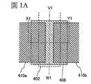
圖1A至圖1C示出電晶體300的結構實例。圖1A是電晶體300的平面圖,圖1B是沿著圖1A的點劃線X1-Y1的剖面圖,並且圖1C是沿著圖1A的點劃線V1-W1的剖面圖。1A to 1C illustrate a structural example of the
電晶體300包括:設置在具有絕緣表面的基板400上的閘極電極層402;閘極電極層402上的閘極絕緣層404;接觸於閘極絕緣層404上並重疊於閘極電極層402的氧化物半導體疊層408;以及電連接於氧化物半導體疊層408的源極電極層410a及汲極電極層410b。另外,電晶體300的構成要素也可以包括覆蓋源極電極層410a及汲極電極層410b並接觸於氧化物半導體疊層408的絕緣層412。The
在電晶體300中,氧化物半導體疊層408包括:接觸於源極電極層410a及汲極電極層410b的氧化物半導體層408a;以及設置在氧化物半導體層408b與閘極絕緣層404之間的氧化物半導體層408b。In the
在氧化物半導體疊層408中,氧化物半導體層408b是形成電晶體300的通道的區域。此外,設置在氧化物半導體層408b的背通道一側的氧化物半導體層408a用作防止源極電極層410a及汲極電極層410b的構成元素擴散到氧化物半導體層408b的緩衝層。就是說,氧化物半導體層408a作為雜質包含源極電極層410a及汲極電極層410b的構成元素。藉由設置該緩衝層,可以抑制在電晶體300的通道中形成陷阱能階,由此可以抑制起因於陷阱能階的S值的增大。因此,藉由抑制電晶體的電特性的不均勻或隨時間的劣化,可以提供可靠性高的半導體裝置。In the
氧化物半導體層408a及氧化物半導體層408b既可以使氧化物半導體層408a與氧化物半導體層408b的構成元素彼此不同,又可以使兩者的構成元素相同但組成不同。但是,作為用作電晶體300的通道的氧化物半導體層408b,較佳為應用場效應遷移率高的氧化物半導體。In the
例如,當使氧化物半導體層408a及氧化物半導體層408b的構成元素相同並使用至少含有銦及鎵的氧化物半導體時,作為氧化物半導體層408b較佳為使用銦的組成大於鎵的組成的氧化物半導體,作為氧化物半導體層408a,較佳為使用銦的組成為鎵的組成以下的氧化物半導體。For example, when the constituent elements of the
在氧化物半導體中,重金屬的s軌道主要有助於載流子傳導,並藉由使銦的含有率增多來呈現s軌道的重疊較多的傾向。因此,藉由在氧化物半導體層408b中使銦的組成大於鎵的組成,可以與銦的組成為鎵的組成以下的氧化物相比具有高場效應遷移率。In an oxide semiconductor, the s orbital of a heavy metal mainly contributes to carrier conduction, and by increasing the content of indium, the s orbital tends to overlap more. Therefore, by making the composition of indium larger than that of gallium in the
另外,由於對其他的金屬元素的鎵的比率越大,金屬氧化物的能隙越大,所以氧化物半導體層408a藉由使銦的組成為鎵的組成以下來具有比氧化物半導體層408b大的能隙。因此,可以在氧化物半導體層408b與氧化物半導體層408a之間形成導電帶能帶偏移,所以是較佳的。此外,由於鎵的氧缺損的形成能量比銦大,所以鎵不容易產生氧缺損。由此,與銦的組成大於鎵的組成的金屬氧化物相比,銦的組成為鎵的組成以下的金屬氧化物具有穩定的特性。由此,可以使電晶體300的背通道一側進一步穩定化。In addition, the larger the ratio of gallium to other metal elements, the larger the energy gap of the metal oxide. Therefore, the
例如,在將In-Ga-Zn類氧化物半導體用於氧化物半導體層408a及氧化物半導體層408b時,作為氧化物半導體層408a,可以使用具有In:Ga:Zn=1:1:1(=1/3:1/3:1/3)、In:Ga:Zn=1:3:2(=1/6:3/6:2/6)、In:Ga:Zn=2:4:3(=2/9:4/9:3/9)或In:Ga:Zn=1:5:3(=1/9:5/9:3/9)的組成(原子數比)的In-Ga-Zn類氧化物或與該組成相似的金屬氧化物。作為氧化物半導體層408b,可以使用具有In:Ga:Zn=3:1:2(=3/6:1/6:2/6)、In:Ga:Zn=4:2:3(=4/9:2/9:3/9)、In:Ga:Zn=5:1:3(=5/9:1/9:3/9)、In:Ga:Zn=5:3:4(=5/12:3/12:4/12)、In:Ga:Zn=6:2:4(=6/12:2/12:4/12)或In:Ga:Zn=7:1:3(=7/11:1/11:3/11)的組成(原子數比)的In-Ga-Zn類氧化物或與該組成相似的金屬氧化物。For example, when an In-Ga-Zn-based oxide semiconductor is used for the
注意,例如In、Ga、Zn的組成為In:Ga:Zn=a:b:c(a+b+c=1)的氧化物的組成近於組成為In:Ga:Zn=A:B:C(A+B+C=1)的氧化物的組成是指a、b、c滿足(a-A)2+(b-B)2+(c-C)2
注意,應用於氧化物半導體疊層408的金屬氧化物不侷限於此,根據所需要的電特性(場效應遷移率、臨界值、偏差等)而使用適當的組成的材料,即可。另外,較佳為採用適當的載流子濃度、雜質濃度、缺陷密度、金屬元素及氧的原子數比、原子間距離以及密度等,以得到所需要的電特性。例如,也可以包含其他金屬元素代替鎵。或者,也可以使用不包含鋅的金屬氧化物。但是,在所應用的金屬氧化物的組成中包含鋅時,較容易使被形成的氧化物半導體層成為後述的CAAC-OS(C-Axis Aligned Crystalline Oxide Semiconductor:c軸配向結晶氧化物半導體)膜,所以是較佳的。Note that the metal oxide applied to the
另外,氧化物半導體層可以利用濺射法形成,並藉由使濺射靶材包含銦,可以降低在成膜時產生微粒。由此,較佳為使氧化物半導體層408a及氧化物半導體層408b包含銦。In addition, the oxide semiconductor layer can be formed by a sputtering method, and by including indium in the sputtering target, generation of particles during film formation can be reduced. Therefore, it is preferable that the
下面,對氧化物半導體層的結構進行說明。Next, the structure of the oxide semiconductor layer will be described.
氧化物半導體層大致分為單晶氧化物半導體層和非單晶氧化物半導體層。非單晶氧化物半導體層包括非晶氧化物半導體層、微晶氧化物半導體層、多晶氧化物半導體層及CAAC-OS膜等。The oxide semiconductor layer is roughly classified into a single crystal oxide semiconductor layer and a non-single crystal oxide semiconductor layer. The non-single crystal oxide semiconductor layer includes an amorphous oxide semiconductor layer, a microcrystalline oxide semiconductor layer, a polycrystalline oxide semiconductor layer, a CAAC-OS film, and the like.
非晶氧化物半導體層具有無序的原子排列並不具有結晶成分。其典型例子是在微小區域中也不具有結晶部而膜整體具有完全的非晶結構的氧化物半導體層。The amorphous oxide semiconductor layer has a disordered atomic arrangement and does not have a crystalline component. A typical example of this is an oxide semiconductor layer in which the entire film has a complete amorphous structure without even having a crystal part in a minute region.
微晶氧化物半導體層例如包括1nm以上且小於10nm的尺寸的微晶(也稱為奈米晶)。因此,微晶氧化物半導體層的原子排列的有序度比非晶氧化物半導體層高。因此,微晶氧化物半導體層的缺陷態密度低於非晶氧化物半導體層。The microcrystalline oxide semiconductor layer includes, for example, microcrystals (also referred to as nanocrystals) having a size of 1 nm or more and less than 10 nm. Therefore, the order degree of atomic arrangement of the microcrystalline oxide semiconductor layer is higher than that of the amorphous oxide semiconductor layer. Therefore, the density of defect states of the microcrystalline oxide semiconductor layer is lower than that of the amorphous oxide semiconductor layer.
CAAC-OS膜是包含多個結晶部的氧化物半導體層之一,大部分的結晶部的尺寸為能夠容納於一邊短於100nm的立方體內的尺寸。因此,有時包括在CAAC-OS膜中的結晶部的尺寸為能夠容納於一邊短於10nm、短於5nm或短於3nm的立方體內的尺寸。CAAC-OS膜的缺陷態密度低於微晶氧化物半導體層。下面,對CAAC-OS膜進行詳細的說明。The CAAC-OS film is one of oxide semiconductor layers including a plurality of crystal parts, and most of the crystal parts have a size that can be accommodated in a cube with one side shorter than 100 nm. Therefore, the size of the crystal part included in the CAAC-OS film is sometimes a size that can be accommodated in a cube whose one side is shorter than 10 nm, shorter than 5 nm, or shorter than 3 nm. The defect state density of the CAAC-OS film is lower than that of the microcrystalline oxide semiconductor layer. Next, the CAAC-OS film will be described in detail.
在CAAC-OS膜的透射電子顯微鏡(TEM:Transmission Electron Microscope)影像中,觀察不到結晶部與結晶部之間的明確的邊界,即晶界(grain boundary)。因此,在CAAC-OS膜中,不容易發生起因於晶界的電子遷移率的降低。In the transmission electron microscope (TEM: Transmission Electron Microscope) image of the CAAC-OS film, a clear boundary between crystal parts, that is, a grain boundary (grain boundary) was not observed. Therefore, in the CAAC-OS film, the cause does not easily occurDecreased electron mobility at grain boundaries.
根據從大致平行於樣本面的方向觀察的CAAC-OS膜的TEM影像(剖面TEM影像)可知在結晶部中金屬原子排列為層狀。各金屬原子層具有反映形成CAAC-OS膜的面(也稱為被形成面)或CAAC-OS膜的頂面的凸凹的形狀並以平行於CAAC-OS膜的被形成面或頂面的方式排列。From the TEM image (cross-sectional TEM image) of the CAAC-OS film observed from the direction substantially parallel to the sample surface, it was found that the metal atoms were arranged in layers in the crystal portion. Each metal atomic layer has a shape reflecting the convex and concave shape of the surface on which the CAAC-OS film is formed (also referred to as the surface to be formed) or the top surface of the CAAC-OS film and is parallel to the surface to be formed or the top surface of the CAAC-OS film arrangement.
另一方面,根據從大致垂直於樣本面的方向觀察的CAAC-OS膜的TEM影像(平面TEM影像)可知在結晶部中金屬原子排列為三角形狀或六角形狀。但是,在不同的結晶部之間金屬原子的排列沒有規律性。On the other hand, from the TEM image (planar TEM image) of the CAAC-OS film observed from the direction substantially perpendicular to the sample surface, it was found that the metal atoms were arranged in a triangular shape or a hexagonal shape in the crystal part. However, there is no regularity in the arrangement of metal atoms between different crystal parts.
由剖面TEM影像及平面TEM影像可知,CAAC-OS膜的結晶部具有配向性。From the cross-sectional TEM image and the planar TEM image, it can be seen that the crystal portion of the CAAC-OS film has orientation.
使用X射線繞射(XRD:X-Ray Diffraction)裝置對CAAC-OS膜進行結構分析。例如,當利用out-of-plane法分析包括InGaZnO4的結晶的CAAC-OS膜時,在繞射角(2θ)為31°附近時出現峰值。由於該峰值來源於InGaZnO4結晶的(009)面,由此可以確認CAAC-OS膜中的結晶具有c軸配向性,並且c軸朝向大致垂直於CAAC-OS膜的被形成面或頂面的方向。Structural analysis of the CAAC-OS film was performed using an X-ray diffraction (XRD: X-Ray Diffraction) apparatus.For example, when a CAAC-OS film including a crystal of InGaZnO 4 is analyzed by the out-of-plane method, a peak appears when the diffraction angle (2θ) is around 31°. This peak is derived (009) plane of the InGaZnO4 crystal, whereby it was confirmed CAAC-OS film having a crystal c-axis orientation and the c-axes substantially perpendicular to the CAAC-OS film formation surface or a top surface direction.
另一方面,當利用從大致垂直於c軸的方向使X線入射到樣本的in-plane法分析CAAC-OS膜時,在2θ為56°附近時出現峰值。該峰值來源於InGaZnO4結晶的(110)面。在此,將2θ固定為56°附近並在以樣本面的法線向量為軸(


由上述結果可知,在具有c軸配向的CAAC-OS膜中,雖然a軸及b軸的方向在結晶部之間不同,但是c軸都朝向平行於被形成面或頂面的法線向量的方向。因此,在上述剖面TEM影像中觀察到的排列為層狀的各金屬原子層相當於與結晶的ab面平行的面。From the above results, in the CAAC-OS film having the c-axis alignment, although the directions of the a-axis and the b-axis are different between the crystal parts, the c-axis is oriented parallel to the normal vector of the surface to be formed or the top surface. direction. Therefore, each metal atomic layer arranged in a layered shape observed in the cross-sectional TEM image corresponds to a plane parallel to the ab plane of the crystal.
注意,結晶部在形成CAAC-OS膜或進行加熱處理等晶化處理時形成。如上所述,結晶的c軸朝向平行於CAAC-OS膜的被形成面或頂面的法線向量的方向。由此,例如,當CAAC-OS膜的形狀因蝕刻等而發生改變時,結晶的c軸不一定平行於CAAC-OS膜的被形成面或頂面的法線向量。Note that the crystallized portion is formed when forming the CAAC-OS film or performing crystallization treatment such as heat treatment. As described above, the c-axis of the crystal is oriented in the direction parallel to the normal vector of the surface or top surface of the CAAC-OS film. Thus, for example, when the shape of the CAAC-OS film is changed by etching or the like, the c-axis of the crystal is not necessarily parallel to the normal vector of the surface on which the CAAC-OS film is formed or the top surface.
此外,CAAC-OS膜中的晶化度不一定均勻。例如,當CAAC-OS膜的結晶部是由CAAC-OS膜的頂面近旁的結晶成長而形成時,有時頂面附近的晶化度高於被形成面附近的晶化度。另外,當對CAAC-OS膜添加雜質時,被添加了雜質的區域的晶化度改變,所以有時CAAC-OS膜中的晶化度根據區域而不同。Furthermore, the degree of crystallinity in the CAAC-OS film is not necessarily uniform. For example, when the crystal part of the CAAC-OS film is formed by the growth of crystals near the top surface of the CAAC-OS film, the crystallinity near the top surface may be higher than the crystallinity near the surface to be formed. In addition, when an impurity is added to the CAAC-OS film, the degree of crystallinity of the region to which the impurity is added changes, so the degree of crystallinity in the CAAC-OS film may differ depending on the region.
注意,當利用out-of-plane法分析包括InGaZnO4結晶的CAAC-OS膜時,除了在2θ為31°附近的峰值之外,有時還在2θ為36°附近觀察到峰值。2θ為36°附近的峰值意味著CAAC-OS膜的一部分中含有不具有c軸配向的結晶。較佳的是,在CAAC-OS膜中在2θ為31°附近時出現峰值而在2θ為36°附近時不出現峰值。Note that when the CAAC-OS film including the InGaZnO 4 crystal was analyzed by the out-of-plane method, in addition to the peak around 31° in 2θ, a peak was sometimes observed around 36° in 2θ. A peak near 36° in 2θ means that a part of the CAAC-OS film contains crystals that do not have c-axis alignment. Preferably, in the CAAC-OS film, the peak appears when 2θ is around 31° and the peak does not appear when 2θ is around 36°.
在使用CAAC-OS膜的電晶體中,起因於可見光或紫外光的照射的電特性的變動小。因此,該電晶體具有高可靠性。In the transistor using the CAAC-OS film, variation in electrical properties due to irradiation with visible light or ultraviolet light is small. Therefore, the transistor has high reliability.
注意,氧化物半導體層例如也可以是包括非晶氧化物半導體層、微晶氧化物半導體層和CAAC-OS膜中的兩種以上的疊層膜。Note that the oxide semiconductor layer may be, for example, a stacked film including two or more of an amorphous oxide semiconductor layer, a microcrystalline oxide semiconductor layer, and a CAAC-OS film.
CAAC-OS膜例如可以使用多晶的金屬氧化物半導體濺射靶材且利用濺射法形成。當離子碰撞到該濺射用靶材時,有時包含在濺射用靶材中的結晶區域從a-b面劈開,即具有平行於a-b面的面的平板狀或顆粒狀的濺射粒子剝離。此時,藉由該平板狀的濺射粒子保持結晶狀態到達基板,可以形成CAAC-OS膜。The CAAC-OS film can be formed by a sputtering method using, for example, a polycrystalline metal oxide semiconductor sputtering target. When ions collide with the sputtering target, the crystal region included in the sputtering target may be cleaved from the a-b plane, that is, tabular or granular sputtering particles having a plane parallel to the a-b plane may be peeled off. At this time, the CAAC-OS film can be formed by the flat sputtered particles reaching the substrate while maintaining the crystalline state.
另外,為了形成CAAC-OS膜,較佳為應用如下條件。In addition, in order to form the CAAC-OS film, the following conditions are preferably applied.
藉由降低成膜時的雜質的混入,可以抑制因雜質導致的結晶狀態損壞。例如,可以降低存在於成膜室內的雜質(氫、水、二氧化碳及氮等)的濃度。另外,可以降低成膜氣體中的雜質濃度。明確而言,使用露點為-80℃以下,較佳為-100℃以下的成膜氣體。By reducing the contamination of impurities during film formation, it is possible to suppress deterioration of the crystal state due to impurities. For example, the concentration of impurities (hydrogen, water, carbon dioxide, nitrogen, etc.) existing in the film formation chamber can be reduced. In addition, the impurity concentration in the film-forming gas can be reduced. Specifically, a film-forming gas having a dew point of -80°C or lower, preferably -100°C or lower is used.
另外,藉由提高成膜時的基板加熱溫度,在濺射粒子附著到基板之後發生濺射粒子的遷移。明確而言,在將基板加熱溫度設定為100℃以上且740℃以下,較佳為200℃以上且500℃以下的狀態下進行成膜。藉由提高成膜時的基板加熱溫度,當平板狀的濺射粒子到達基板時,在基板上發生遷移,濺射粒子的平坦的面附著到基板。In addition, by increasing the substrate heating temperature during film formation, sputtering particlesMigration of sputtered particles occurs after attachment to the substrate. Specifically, film formation is performed in a state where the substrate heating temperature is set to 100° C. or higher and 740° C. or lower, preferably 200° C. or higher and 500° C. or lower. By increasing the substrate heating temperature during film formation, when the flat sputtered particles reach the substrate, they migrate on the substrate, and the flat surfaces of the sputtered particles adhere to the substrate.
另外,較佳的是,藉由增高成膜氣體中的氧比例並對電力進行最優化,減輕成膜時的電漿損傷。將成膜氣體中的氧比例設定為30vol%以上,較佳為100vol%。In addition, it is preferable to reduce the plasma damage during film formation by increasing the oxygen ratio in the film formation gas and optimizing the electric power. The oxygen ratio in the film-forming gas is set to 30 vol% or more, preferably 100 vol%.
以下,作為濺射用金屬氧化物靶材的一個例子,示出In-Ga-Zn-O化合物靶材。Hereinafter, an In-Ga-Zn-O compound target is shown as an example of the metal oxide target for sputtering.
將InOX粉末、GaOY粉末及ZnOZ粉末以預定的比率混合,進行加壓處理,然後在1000℃以上且1500℃以下的溫度下進行加熱處理,由此得到作為多晶的In-Ga-Zn-O化合物靶材。另外,X、Y及Z為任意正數。在此,InOX粉末、GaOY粉末及ZnOZ粉末的預定的莫耳數比例如為2:2:1、8:4:3、3:1:1、1:1:1、4:2:3或3:1:2。另外,粉末的種類及其混合莫耳數比可以根據所製造的濺射用靶材適當地改變。InOX powder, GaOY powder, and ZnOZ powder are mixed at a predetermined ratio, subjected to pressure treatment, and then heat-treated at a temperature of 1000° C. or higher and 1500° C. or lower, thereby obtaining In-Ga- Zn-O compound target. In addition, X, Y and Z are arbitrary positive numbers. Here,the predetermined molar ratios of the InO X powder, the GaOY powder, and the ZnOZ powder are, for example, 2:2:1, 8:4:3, 3:1:1, 1:1:1, and 4:2 :3 or 3:1:2. In addition, the kind of powder and its mixed molar ratio can be appropriately changed according to the sputtering target to be produced.
另外,也可以使氧化物半導體層408a的結晶性與氧化物半導體層408b不同。但是,作為用作電晶體300的通道的氧化物半導體層408b,較佳為應用CAAC-OS膜。此外,在氧化物半導體層408b是CAAC-OS膜時,在氧化物半導體層408b上並與其接觸的氧化物半導體層408a中發生前驅物(precursor)的排列,藉由使該層具有所謂秩序性,有時可以使氧化物半導體層408a成為CAAC-OS膜。在設置在背通道一側的氧化物半導體層408a是非晶氧化物半導體的情況下,由於形成源極電極層410a及汲極電極層410b時的蝕刻處理容易產生氧缺損而被n型化。因此,較佳為將具有結晶性的氧化物半導體應用於氧化物半導體層408a。In addition, the crystallinity of the
此外,在本實施方式中,氧化物半導體層408a和氧化物半導體層408b是使用相同構成元素形成的氧化物半導體疊層。此時,根據材料或成膜條件,各氧化物半導體層之間的介面有時不明確。因此,在圖1A至圖1C中,以虛線示意性地示出氧化物半導體層408a和氧化物半導體層408b的介面。這是與後面的各圖式同樣。In addition, in this embodiment mode, the
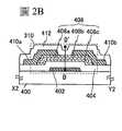
圖2A至圖2C示出電晶體310的結構實例。圖2A是電晶體310的平面圖,圖2B是沿著圖2A的點劃線X2-Y2的剖面圖,圖2C是沿著圖2A的點劃線V2-W2的剖面圖。與圖1A至圖1C所示的電晶體300同樣,圖2A至圖2C所示的電晶體310包括:設置在具有絕緣表面的基板400上的閘極電極層402;閘極電極層402上的閘極絕緣層404;接觸於閘極絕緣層404上並重疊於閘極電極層402的氧化物半導體疊層408;以及電連接於氧化物半導體疊層408的源極電極層410a及汲極電極層410b。另外,電晶體310的構成要素也可以包括覆蓋源極電極層410a及汲極電極層410b並接觸於氧化物半導體疊層408的絕緣層412。2A to 2C illustrate a structural example of the
電晶體310與電晶體300不同之處是:電晶體310在氧化物半導體層408b與閘極絕緣層404之間包括氧化物半導體層408c。就是說,在電晶體310中,氧化物半導體疊層408具有氧化物半導體層408a、氧化物半導體層408b及氧化物半導體層408c的疊層結構。The difference between the
注意,除了氧化物半導體層408c之外,電晶體310的結構與電晶體300相同,而可以參照關於電晶體300的說明。Note that the structure of the
藉由在電晶體310中的形成通道的氧化物半導體層408b與閘極絕緣層404之間設置氧化物半導體層408c,成為載流子流過離閘極絕緣層404遠的區域的結構(所謂埋入通道)。由此,可以使閘極絕緣層404與通道的介面穩定化,而可以抑制在該介面形成陷阱能階。由此,防止電晶體的劣化,尤其是光負偏壓劣化等光劣化,而可以製造可靠性高的電晶體。By arranging the
在含有銦和鎵的金屬氧化物中,對其他金屬元素的鎵的組成的比率越大,能隙越大。此外,由於氧化物半導體層408c與氧化物半導體層408b之間的帶隙之差形成導電帶能帶偏移。因此,當作為氧化物半導體層408c使用銦的組成為鎵的組成以下的金屬氧化物時,在氧化物半導體層408b中能夠有效地形成通道,所以是較佳的。In the metal oxide containing indium and gallium, the larger the composition ratio of gallium to other metal elements, the larger the energy gap. Further, a conduction band energy band shift is formed due to the difference in the band gap between the
在將In-Ga-Zn類氧化物半導體用於氧化物半導體層408c時,作為氧化物半導體層408c,可以使用具有In:Ga:Zn=1:1:1(=1/3:1/3:1/3)、In:Ga:Zn=1:3:2(=1/6:3/6:2/6)、In:Ga:Zn=2:4:3(=2/9:4/9:3/9)或In:Ga:Zn=1:5:3(=1/9:5/9:3/9)的組成(原子數比)的In-Ga-Zn類氧化物或與該組成相似的氧化物。另外,作為氧化物半導體層408a和氧化物半導體層408c較佳為都使用銦的組成為鎵的組成以下的金屬氧化物。在此,氧化物半導體層408a的組成與氧化物半導體層408c的組成既可以是相同,又可以是不同。When an In-Ga-Zn-based oxide semiconductor is used for the
另外,一般而言,氧化物半導體層的大部分利用濺射法形成。另一方面,當對氧化物半導體層進行蝕刻時,有時被離子化的稀有氣體元素(例如,氬)或從濺射靶材表面彈出的粒子將閘極絕緣層等的成為氧化物半導體層的被形成面的膜的粒子彈出。因此,從成為被形成面的膜彈出的粒子作為雜質元素進入到氧化物半導體層。尤其是,有高濃度的雜質元素進入到被形成面附近的氧化物半導體層中的擔憂。另外,當雜質元素殘留在被形成面附近的氧化物半導體層中時,該氧化物半導體層高電阻化而成為電晶體的電特性的下降的原因。In addition, in general, most of the oxide semiconductor layers are formed by the sputtering method. On the other hand, when the oxide semiconductor layer is etched, ionized rare gas elements (eg, argon) or particles ejected from the surface of the sputtering target may turn the gate insulating layer or the like into an oxide semiconductor layer. The particles of the film formed by the surface are ejected. Therefore, the particles ejected from the film to be the surface to be formed enter the oxide semiconductor layer as impurity elements. In particular, there is a concern that a high concentration of impurity elements may enter the oxide semiconductor layer in the vicinity of the surface to be formed. In addition, when the impurity element remains in the oxide semiconductor layer in the vicinity of the surface to be formed, the resistance of the oxide semiconductor layer is increased, which causes a decrease in the electrical characteristics of the transistor.
然而,在圖2A至圖2C所示的電晶體310中,藉由在形成通道的氧化物半導體層408b與閘極絕緣層404之間包括氧化物半導體層408c,可以抑制閘極絕緣層404的構成元素擴散到通道中。就是說,氧化物半導體層408c有時作為雜質包含閘極絕緣層404的構成元素(例如,矽)。藉由包括氧化物半導體層408c,可以使電晶體310的電特性進一步穩定化,而可以提供可靠性高的半導體裝置。However, in the
另外,圖2D是示出圖2B中的厚度方向(D-D’間)上的能帶圖。在本實施方式中,使用In-Ga-Zn類氧化物半導體形成氧化物半導體層408a至氧化物半導體層408c。此外,作為氧化物半導體層408g及氧化物半導體層408c應用銦的組成為鎵的組成以下的金屬氧化物,作為氧化物半導體層408b應用銦的組成大於鎵的組成的金屬氧化物。由此,如圖2D的能帶圖所示,本實施方式所示的氧化物半導體疊層408能夠構成所謂埋入通道。In addition, Fig. 2D is a diagram showing an energy band diagram in the thickness direction (between D-D') in Fig. 2B . In this embodiment mode, the
以下,使用圖3A至圖3D示出電晶體310的製造方法的一個例子。Hereinafter, an example of a method of manufacturing the
首先,在具有絕緣表面的基板400上形成閘極電極層402(包括用與此相同的層形成的佈線)。First, a gate electrode layer 402 (including wiring formed with the same layer) is formed on a
對可用作具有絕緣表面的基板400的基板沒有特別的限制,但是基板400需要至少具有能夠承受後面進行的熱處理的程度的耐熱性。例如,可以使用玻璃基板如硼矽酸鋇玻璃和硼矽酸鋁玻璃等、陶瓷基板、石英基板、藍寶石基板等。另外,作為基板400,可以採用以矽或碳化矽等為材料的單晶半導體基板或多晶半導體基板、以矽鍺為材料的化合物半導體基板、SOI基板等,並且也可以使用在這些基板上設置有半導體元件的基板。此外,也可以在基板400上形成基底絕緣層。There is no particular limitation on the substrate that can be used as the
可以使用諸如鉬、鈦、鉭、鎢、鋁、銅、鉻、釹、鈧等的金屬材料或以這些材料為主要成分的合金材料來形成閘極電極層402。此外,閘極電極層402可以使用以摻雜有磷等雜質元素的多晶矽膜為代表的半導體膜、鎳矽化物等矽化物膜。閘極電極層402既可以是單層結構,又可以是疊層結構。也可以使閘極電極層402具有錐形形狀,例如可以將錐角設定為15°以上且70°以下。在此,錐角是指具有錐形形狀的層的側面與該層的底面之間的角度。The
另外,作為閘極電極層402的材料還可以使用氧化銦氧化錫、含有氧化鎢的氧化銦、含有氧化鎢的氧化銦鋅、含有氧化鈦的氧化銦、含有氧化鈦的氧化銦錫、氧化銦氧化鋅、添加有氧化矽的氧化銦錫等導電材料。In addition, as the material of the
或者,作為閘極電極層402的材料還可以使用含有氮的In-Ga-Zn類氧化物、含有氮的In-Sn類氧化物、含有氮的In-Ga類氧化物、含有氮的In-Zn類氧化物、含有氮的Sn類氧化物、含有氮的In類氧化物、金屬氮化物膜(氮化銦膜、氮化鋅膜、氮化鉭模、氮化鎢膜等)。由於上述材料具有5電子伏特以上的功函數,所以藉由使用上述材料形成閘極電極層402,可以使電晶體的臨界電壓成為正值,由此可以實現常截止(normally-off)的開關電晶體。Alternatively, as the material of the
接著,以覆蓋閘極電極層402的方式在閘極電極層402上形成閘極絕緣層404(參照圖3A)。作為閘極絕緣層404,藉由電漿CVD法、濺射法等以單層或疊層形成包含選自氧化矽膜、氧氮化矽膜、氮氧化矽膜、氮化矽膜、氧化鋁膜、氧化鉿膜、氧化釔膜、氧化鋯膜、氧化鎵膜、氧化鉭膜、氧化鎂膜、氧化鑭膜、氧化鈰膜和氧化釹膜中的一種以上的絕緣膜。Next, a
另外,在閘極絕緣層404中,接觸於後面形成的氧化物半導體疊層408的區域較佳是氧化物絕緣層,更佳為包括氧過剩區。為了在閘極絕緣層404設置氧過剩區,例如在氧氛圍下形成閘極絕緣層404即可。或者,也可以將氧引入到成膜後的閘極絕緣層404中而形成氧過剩區。作為氧的引入方法,可以使用離子植入法、離子摻雜法、電漿浸沒離子佈植技術、電漿處理等。In addition, in the
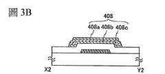
接著,在閘極絕緣層404上依次形成成為氧化物半導體層408c的氧化物半導體膜、成為氧化物半導體層408b的氧化物半導體膜及成為氧化物半導體層408a的氧化物半導體膜,藉由利用光微影法的蝕刻處理將這些氧化物半導體膜加工為島狀,來形成氧化物半導體疊層408(參照圖3B)。Next, an oxide semiconductor film to become the
氧化物半導體層408c、氧化物半導體層408b及氧化物半導體層408a分別既可以是非晶氧化物半導體,又可以是結晶氧化物半導體。但是,作為用作電晶體310的通道的氧化物半導體層408b,較佳為使用結晶氧化物半導體。此外,藉由對非晶氧化物半導體進行熱處理,可以形成結晶氧化物半導體。將使非晶氧化物半導體晶化的熱處理的溫度設定為250℃以上且700℃以下,較佳為400℃以上,更佳為500℃以上,進一步較佳為550℃以上。該熱處理也可以兼作製程中的其他加熱處理。The
作為各氧化物半導體膜的成膜方法,可以適當地利用濺射法、MBE(Molecular Beam Epitaxy:分子束磊晶)法、CVD法、脈衝雷射沉積法、ALD(Atomic Layer Deposition:原子層沉積)法等。As the film-forming method of each oxide semiconductor film, it can be appropriately usedSputtering method, MBE (Molecular Beam Epitaxy: molecular beam epitaxy) method, CVD method, pulsed laser deposition method, ALD (Atomic Layer Deposition: atomic layer deposition) method, etc.
當形成氧化物半導體膜時,較佳為盡可能地降低膜中的氫濃度。為了降低氫濃度,例如,在藉由濺射法進行成膜時,作為供應到濺射裝置的成膜室內的氛圍氣體適當地使用:如氫、水、羥基或者氫化物等雜質被去除的高純度的稀有氣體(典型的有氬)、氧、稀有氣體和氧的混合氣體。When forming an oxide semiconductor film, it is preferable to reduce the hydrogen concentration in the film as much as possible. In order to reduce the hydrogen concentration, for example, when forming a film by the sputtering method, it is appropriate to use it as an atmosphere gas supplied into the film forming chamber of the sputtering apparatus: a high level of which impurities such as hydrogen, water, hydroxyl or hydride are removed. Pure rare gas (typically argon), oxygen, a mixture of rare gas and oxygen.
另外,藉由在去除殘留在成膜室內的水分的同時引入去除了氫及水分的濺射氣體來進行成膜,可以降低形成的氧化物半導體膜的氫濃度。為了去除殘留在成膜室內的水分,較佳為使用吸附型真空泵,例如,低溫泵、離子泵、鈦昇華泵。此外,也可以使用具備冷阱的渦輪泵。由於低溫泵對如氫分子、水(H2O)等包含氫原子的化合物(較佳為還包括包含碳原子的化合物)等進行排出的能力較高,所以可以降低使用該低溫泵進行排氣的成膜室中形成的膜中的雜質濃度。In addition, the hydrogen concentration of the oxide semiconductor film to be formed can be reduced by introducing a sputtering gas from which hydrogen and moisture have been removed while removing the moisture remaining in the film-forming chamber to form a film. In order to remove the moisture remaining in the film-forming chamber, it is preferable to use an adsorption-type vacuum pump, for example, a cryopump, an ion pump, and a titanium sublimation pump. In addition, a turbo pump with a cold trap can also be used. Since the cryopump has a high ability to discharge compounds containing hydrogen atoms such as hydrogen molecules, water (H2 O) (preferably, compounds containing carbon atoms), etc., the use of the cryopump for exhaust gas can be reduced. The impurity concentration in the film formed in the film formation chamber.
另外,較佳為以不暴露於大氣的方式連續地形成閘極絕緣層404和氧化物半導體膜。藉由以不暴露於大氣的方式連續地形成閘極絕緣層404和氧化物半導體膜,可以防止氫或氫化合物(例如,水等)附著於氧化物半導體膜表面,所以可以抑制雜質的混入。In addition, it is preferable to continuously form the
另外,在藉由濺射法形成氧化物半導體膜的情況下,使用於成膜的金屬氧化物靶材的相對密度(填充率)為90%以上且100%以下,較佳為95%以上且99.9%以下。藉由使用相對密度高的金屬氧化物靶材,可以形成緻密的膜。In addition, in the case of forming the oxide semiconductor film by the sputtering method,The relative density (filling rate) of the metal oxide target used for film formation is 90% or more and 100% or less, preferably 95% or more and 99.9% or less. A dense film can be formed by using a metal oxide target with a high relative density.
另外,為了降低有可能包含在氧化物半導體膜中的雜質的濃度,在將基板400保持為高溫的狀態下形成氧化物半導體膜也是有效的。將加熱基板400的溫度設定為150℃以上且450℃以下,較佳為將基板溫度設定為200℃以上且350℃以下即可。另外,藉由在進行成膜時以高溫加熱基板,可以形成結晶氧化物半導體膜。In addition, in order to reduce the concentration of impurities that may be contained in the oxide semiconductor film, it is also effective to form the oxide semiconductor film while maintaining the
當作為氧化物半導體層(例如,氧化物半導體層408b)使用CAAC-OS膜時,作為獲得該CAAC-OS膜的方法,例如可以將成膜溫度設定為200℃以上且450℃以下來形成氧化物半導體膜,而實現大致垂直於其表面的c軸配向。或者,也可以在形成薄的氧化物半導體膜之後,進行200℃以上且700℃以下的加熱處理,而實現大致垂直於其表面的c軸配向。或者,也可以在形成薄的第一層之後,進行200℃以上且700℃以下的加熱處理,然後形成第二層,而實現大致垂直於其表面的c軸配向。When a CAAC-OS film is used as the oxide semiconductor layer (for example, the
用於氧化物半導體層408a至氧化物半導體層408c的氧化物半導體至少含有銦(In)。尤其較佳為含有銦及鋅(Zn)。此外,作為用來減小使用該氧化物半導體的電晶體的電特性的不均勻的穩定劑(stabilizer),較佳為除了上述元素以外還含有鎵(Ga)。The oxide semiconductor used for the
另外,如上所述,作為用作用來降低陷阱能階的影響的緩衝層的氧化物半導體層408a及氧化物半導體層408c,較佳為使用銦的組成為鎵的組成以下的金屬氧化物,作為成為通道形成區的氧化物半導體層408b,較佳為使用銦的組成大於鎵的組成的金屬氧化物。In addition, as described above, as the
此外,作為穩定劑,也可以代替鎵(Ga)或加上鎵(Ga)還包含錫(Sn)、鉿(Hf)、鋁(Al)和鋯(Zr)中的一種或多種。另外,作為其他穩定劑,也可以含有鑭系元素的鑭(La)、鈰(Ce)、鐠(Pr)、釹(Nd)、釤(Sm)、銪(Eu)、釓(Gd)、鋱(Tb)、鏑(Dy)、鈥(Ho)、鉺(Er)、銩(Tm)、鐿(Yb)、鎦(Lu)中的一種或多種。In addition, as a stabilizer, one or more of tin (Sn), hafnium (Hf), aluminum (Al), and zirconium (Zr) may also be included in place of or in addition to gallium (Ga). In addition, as other stabilizers, lanthanum (La), cerium (Ce), pyridine (Pr), neodymium (Nd), samarium (Sm), europium (Eu), gadolinium (Gd), and xiuminium may be contained as other stabilizers. One or more of (Tb), dysprosium (Dy), ∥ (Ho), erbium (Er), tin (Tm), ytterbium (Yb), and tium (Lu).
例如,作為氧化物半導體,可以使用:氧化銦、氧化錫、氧化鋅;二元金屬氧化物的In-Zn類氧化物、In-Mg類氧化物、In-Ga類氧化物;三元金屬氧化物的In-Ga-Zn類氧化物、In-Al-Zn類氧化物、In-Sn-Zn類氧化物、In-Hf-Zn類氧化物、In-La-Zn類氧化物、In-Ce-Zn類氧化物、In-Pr-Zn類氧化物、In-Nd-Zn類氧化物、In-Sm-Zn類氧化物、In-Eu-Zn類氧化物、In-Gd-Zn類氧化物、In-Tb-Zn類氧化物、In-Dy-Zn類氧化物、In-Ho-Zn類氧化物、In-Er-Zn類氧化物、In-Tm-Zn類氧化物、In-Yb-Zn類氧化物、In-Lu-Zn類氧化物;以及四元金屬氧化物的In-Sn-Ga-Zn類氧化物、In-Hf-Ga-Zn類氧化物、In-Al-Ga-Zn類氧化物、In-Sn-Al-Zn類氧化物、In-Sn-Hf-Zn類氧化物、In-Hf-Al-Zn類氧化物。For example, as oxide semiconductors, indium oxide, tin oxide, and zinc oxide can be used; In-Zn-based oxides, In-Mg-based oxides, and In-Ga-based oxides of binary metal oxides; Ternary metal oxides In-Ga-Zn-based oxides, In-Al-Zn-based oxides, In-Sn-Zn-based oxides, In-Hf-Zn-based oxides, In-La-Zn-based oxides, In-Ce -Zn-based oxides, In-Pr-Zn-based oxides, In-Nd-Zn-based oxides, In-Sm-Zn-based oxides, In-Eu-Zn-based oxides, In-Gd-Zn-based oxides , In-Tb-Zn-based oxides, In-Dy-Zn-based oxides, In-Ho-Zn-based oxides, In-Er-Zn-based oxides, In-Tm-Zn-based oxides, In-Yb- Zn-based oxides, In-Lu-Zn-based oxides; and In-Sn-Ga-Zn-based oxides, In-Hf-Ga-Zn-based oxides, In-Al-Ga-Zn-based oxides of quaternary metal oxides Oxides, In-Sn-Al-Zn Oxides, In-Sn-Hf-Zn Oxides,In-Hf-Al-Zn type oxide.
例如,In-Ga-Zn類氧化物是指作為主要成分含有In、Ga、Zn的氧化物,對In、Ga、Zn的比率沒有限制。此外,也可以含有In、Ga、Zn以外的金屬元素。For example, the In-Ga-Zn-based oxide refers to an oxide containing In, Ga, and Zn as main components, and the ratio of In, Ga, and Zn is not limited. In addition, metal elements other than In, Ga, and Zn may be contained.
另外,作為氧化物半導體,也可以使用以InMO3(ZnO)m(m>0,且m不是整數)表示的材料。注意,M表示選自Ga、Fe、Mn和Co中的一種金屬元素或多種金屬元素。另外,作為氧化物半導體,也可以使用以In2SnO5(ZnO)n(n>0,且n是整數)表示的材料。In addition, as an oxide semiconductor,a material represented by InMO 3 (ZnO)m (m>0, and m is not an integer) can also be used. Note that M represents a metal element or metal elements selected from Ga, Fe, Mn, and Co. In addition, as the oxide semiconductor,a material represented by In 2 SnO5 (ZnO)n (n>0, and n is an integer) can also be used.
較佳為對氧化物半導體疊層408進行用來去除過剩的氫(包括水及羥基)(脫水化或脫氫化)的加熱處理。將加熱處理的溫度設定為300℃以上且700℃以下或低於基板的應變點。加熱處理可以在減壓下或氮氛圍下等進行。藉由進行該加熱處理可以去除賦予n型導電性的雜質的氫。The
另外,用於脫水化或脫氫化的加熱處理只要在形成氧化物半導體膜之後就可以在電晶體的製程中的任何時序進行。另外,用於脫水化或脫氫化的加熱處理也可以多次進行,還可以兼作其他加熱處理。In addition, the heat treatment for dehydration or dehydrogenation may be performed at any timing in the process of the transistor as long as the oxide semiconductor film is formed. In addition, the heat treatment for dehydration or dehydrogenation may be performed multiple times, and may also serve as other heat treatments.
在加熱處理中,氮或氦、氖、氬等稀有氣體較佳為不包含水、氫等。另外,較佳為將引入到加熱處理裝置中的氮或氦、氖、氬等稀有氣體的純度設定為6N(99.9999%)以上,較佳為設定為7N(99.99999%)以上(即,將雜質濃度設定為1ppm以下,較佳為設定為0.1ppm以下)。In the heat treatment, it is preferable that nitrogen or noble gases such as helium, neon, and argon do not contain water, hydrogen, and the like. In addition, the purity of nitrogen, helium, neon, argon and other rare gases introduced into the heat treatment device is preferably set to 6N (99.9999%) or more, preferably 7N (99.99999%) or more (that is, impurities The concentration is set to 1 ppm or less, preferably set to0.1ppm or less).
另外,可以在藉由加熱處理對氧化物半導體層(或氧化物半導體疊層)進行加熱之後,在維持該加熱溫度的狀態下或在從該加熱溫度降溫的過程中,對相同爐內引入高純度的氧氣體、高純度的一氧化二氮氣體或超乾燥空氣(使用CRDS(Cavity Ring Down laser Spectroscopy:光腔衰蕩光譜法)方式的露點計進行測試時的水分量是20ppm(露點換算為-55℃)以下,較佳的是1ppm以下,更佳的是10ppb以下的空氣)。較佳為不使氧氣體或一氧化二氮氣體包含水、氫等。或者,較佳為將引入到加熱處理裝置中的氧氣體或一氧化二氮氣體的純度設定為6N以上,較佳為7N以上(也就是說,將氧氣體或一氧化二氮氣體中的雜質濃度設定為1ppm以下,較佳為設定為0.1ppm以下)。即使在利用脫水化處理或脫氫化處理的雜質排出製程中氧化物半導體的主要構成要素的氧減少,也可以藉由利用氧氣體或一氧化二氮氣體供給氧,來使氧化物半導體層高度純化且電性i型(本質)化。In addition, after the oxide semiconductor layer (or oxide semiconductor stack) is heated by the heat treatment, a high temperature can be introduced into the same furnace while maintaining the heating temperature or in the process of decreasing the temperature from the heating temperature. The moisture content of pure oxygen gas, high-purity nitrous oxide gas, or ultra-dry air (using a dew point meter of CRDS (Cavity Ring Down laser Spectroscopy: cavity ring-down spectroscopy) method) is 20 ppm (the dew point is converted to -55°C) or less, preferably 1 ppm or less, more preferably 10 ppb or less of air). It is preferable not to contain water, hydrogen or the like in the oxygen gas or the nitrous oxide gas. Alternatively, the purity of the oxygen gas or nitrous oxide gas introduced into the heat treatment device is preferably set to 6N or more, preferably 7N or more (that is, the impurities in the oxygen gas or nitrous oxide gas are The concentration is set to 1 ppm or less, preferably 0.1 ppm or less). Even if oxygen is reduced in the impurity removal process by dehydration treatment or dehydrogenation treatment, the oxide semiconductor layer can be highly purified by supplying oxygen with oxygen gas or nitrous oxide gas. And electrical i-type (essential) change.
另外,當進行脫水化處理或脫氫化處理時氧有可能脫離而減少,所以可以對經過脫水化處理或脫氫化處理的氧化物半導體層引入氧(至少包括氧自由基、氧原子和氧離子中的一種)來對該層供應氧。In addition, when dehydration treatment or dehydrogenation treatment is performed, oxygen may be desorbed and reduced. Therefore, oxygen (at least oxygen radicals, oxygen atoms and oxygen ions) can be introduced into the oxide semiconductor layer subjected to dehydration treatment or dehydrogenation treatment. a) to supply oxygen to the layer.
藉由對經過脫水化處理或脫氫化處理的氧化物半導體層引入氧而供應氧,可以使氧化物半導體層高度純化且i型(本質)化。包含高度純化了且i型(本質)化了的氧化物半導體的電晶體的電特性變動被抑制,所以該電晶體在電性上穩定。By introducing oxygen to the oxide semiconductor layer subjected to the dehydration treatment or dehydrogenation treatment and supplying oxygen, the oxide semiconductor layer can be highly purified and i-typed (intrinsic). Contains highly purified and i-type (essential) oxygenSince variations in electrical characteristics of the compound semiconductor transistor are suppressed, the transistor is electrically stable.
當對氧化物半導體層引入氧時,既可以對氧化物半導體層直接引入氧,又可以以透過在後面形成的絕緣層的方式對氧化物半導體層引入氧。作為氧(至少包括氧自由基、氧原子和氧離子中的一種)的引入方法,可以使用離子植入法、離子摻雜法、電漿浸沒離子佈植技術、電漿處理等。另外,可以使用含有氧的氣體進行氧的引入處理。作為含有氧的氣體,可以使用氧、一氧化二氮、二氧化氮、二氧化碳、一氧化碳等。此外,在氧的引入處理中,也可以使含有氧的氣體包含稀有氣體。When oxygen is introduced into the oxide semiconductor layer, oxygen may be directly introduced into the oxide semiconductor layer, or oxygen may be introduced into the oxide semiconductor layer through an insulating layer formed later. As an introduction method of oxygen (including at least one of oxygen radicals, oxygen atoms, and oxygen ions), ion implantation, ion doping, plasma immersion ion implantation, plasma treatment, and the like can be used. In addition, the oxygen introduction treatment may be performed using an oxygen-containing gas. As the oxygen-containing gas, oxygen, nitrous oxide, nitrogen dioxide, carbon dioxide, carbon monoxide and the like can be used. In addition, in the oxygen introduction treatment, a rare gas may be contained in the oxygen-containing gas.
例如當藉由離子植入法對氧化物半導體層注入氧離子時,可以將劑量設定為1×10¹³ions/cm2以上且5×1016ions/cm2以下。For example, when implanting oxygen ions into the oxide semiconductor layer by an ion implantation method, the dose can be set to 1×10¹³ ions/cm2 or more and 5×10¹⁶ ions/cm2 or less.
另外,對氧化物半導體層供應氧的製程只要在形成氧化物半導體膜之後就可以在電晶體的製程中的任何時序進行。另外,氧的引入也可以多次進行。In addition, the process of supplying oxygen to the oxide semiconductor layer may be performed at any timing in the process of the transistor as long as the oxide semiconductor film is formed. In addition, the introduction of oxygen may be performed multiple times.
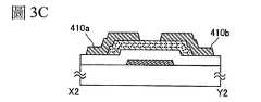
接著,在氧化物半導體疊層408上形成導電膜並對其進行加工來形成源極電極層410a及汲極電極層410b(包括用與此相同的層形成的佈線)(參照圖3C)。Next, a conductive film is formed on the
作為源極電極層410a及汲極電極層410b,例如可以使用含有選自Al、Cr、Cu、Ta、Ti、Mo、W中的元素的金屬膜或以上述元素為成分的金屬氮化物膜(氮化鈦膜、氮化鉬膜、氮化鎢膜)等。另外,還可以在Al、Cu等的金屬膜的下側和上側中的一者或兩者上層疊Ti、Mo、W等的高熔點金屬膜或它們的金屬氮化物膜(氮化鈦膜、氮化鉬膜、氮化鎢膜)。另外,源極電極層410a及汲極電極層410b也可以使用導電金屬氧化物形成。導電金屬氧化物例如可以使用氧化銦(In2O3)、氧化錫(SnO2)、氧化鋅(ZnO)、氧化銦氧化錫(In2O3-SnO2)、氧化銦氧化鋅(In2O3-ZnO)或者使這些金屬氧化物材料含有氧化矽的材料。As the
另外,作為源極電極層410a及汲極電極層410b可以使用含有氮的In-Ga-Zn-O膜、含有氮的In-Sn-O膜、含有氮的In-Ga-O膜、含有氮的In-Zn-O膜、含有氮的Sn-O膜、含有氮的In-O膜等金屬氮化物膜。由於這些膜含有與氧化物半導體疊層408相同的構成元素,所以可以使源極電極層410a或汲極電極層410b與氧化物半導體疊層408之間的介面穩定。In addition, as the
此外,當作為源極電極層410a及汲極電極層410b應用包含銅的導電膜時可以降低佈線電阻,所以是較佳的。一般而言,由於銅容易擴散到半導體或氧化矽膜中,所以有可能使半導體裝置的操作不穩定而使良率明顯降低。但是,由於電晶體310包括接觸於源極電極層410a及汲極電極層410b並用作用來抑制該電極層的構成元素(在此,銅)擴散的緩衝層的氧化物半導體層408a,所以可以降低因銅的擴散而產生的背通道一側的陷阱能階的影響,較佳的是完全抑制背通道一側的陷阱能階的影響。In addition, it is preferable to apply a conductive film containing copper as the
接著,以覆蓋源極電極層410a、汲極電極層410b以及露出的氧化物半導體疊層408的方式形成絕緣層412(參照圖3D)。Next, an insulating
絕緣層412可以利用電漿CVD法、濺射法並使用氧化矽膜、氧化鎵膜、氧化鋁膜、氮化矽膜、氧氮化矽膜、氧氮化鋁膜或者氮氧化矽膜等的單層或疊層形成。注意,當作為絕緣層412形成氧化物絕緣層時,能夠利用該氧化物絕緣層將氧供應到氧化物半導體疊層408,所以是較佳的。The insulating
可以在形成絕緣層412之後進行加熱處理。將加熱處理的溫度較佳為設定為200℃以上,例如可以設定為220℃。The heat treatment may be performed after the insulating
藉由上述步驟可以形成本實施方式的電晶體310。Through the above steps, the
本實施方式所示的電晶體包括:用作抑制源極電極層或汲極電極層的構成元素擴散到通道中的緩衝層的第一氧化物半導體層;以及用作通道的第二氧化物半導體層。由此,可以降低能夠在電晶體的背通道一側形成的介面態的影響。另外,更佳的是,本實施方式所示的電晶體設置在用作通道的氧化物半導體層與閘極絕緣層之間並包括用作用來防止通道的閘極絕緣層一側的介面的劣化的緩衝層的第三氧化物半導體層。藉由包括第三氧化物半導體層,可以減少電晶體的光劣化(例如,光負偏壓劣化),而可以提供可靠性高的半導體裝置。The transistor shown in this embodiment mode includes: a first oxide semiconductor layer serving as a buffer layer for suppressing diffusion of constituent elements of a source electrode layer or a drain electrode layer into a channel; and a second oxide semiconductor layer serving as a channel Floor. Thereby, the influence of the interface state that can be formed on the back channel side of the transistor can be reduced. In addition, it is more preferable that the transistor shown in this embodiment mode is provided between the oxide semiconductor layer serving as the channel and the gate insulating layer and includes the interface serving as the gate insulating layer serving as the channel to prevent deterioration of the side the third oxide semiconductor layer of the buffer layer. By including the third oxide semiconductor layer, optical deterioration of the transistor (eg, optical negative bias deterioration) can be reduced, and a semiconductor device with high reliability can be provided.
以上,本實施方式所示的結構、方法等可以與其他實施方式所示的結構、方法等適當地組合而使用。As described above, the structures, methods, and the like shown in this embodiment can be combined with other implementations.The structures, methods, and the like shown in the embodiments are used in combination as appropriate.
在本實施方式中,參照圖10A和圖10B說明與實施方式1不同的半導體裝置的一個方式。明確而言,說明具有與實施方式1所示的電晶體不同的閘極絕緣層的結構的電晶體。In this embodiment mode, an embodiment of a semiconductor device different from
圖10A示出電晶體320的結構實例。與圖2A至圖2D所示的電晶體310同樣,圖10A所示的電晶體320包括:設置在具有絕緣表面的基板400上的閘極電極層402;閘極電極層402上的閘極絕緣層403、406;接觸於閘極絕緣層406並重疊於閘極電極層402的氧化物半導體疊層408;以及電連接於氧化物半導體疊層408的源極電極層410a及汲極電極層410b。在電晶體320中,氧化物半導體疊層408包括:接觸於閘極絕緣層406的氧化物半導體層408c;在氧化物半導體層408c上並與其接觸的氧化物半導體層408b;在氧化物半導體層408b上並與其接觸的接觸於源極電極層410a及汲極電極層410b的氧化物半導體層408a。另外,電晶體320的構成要素也可以包括覆蓋源極電極層410a及汲極電極層410b並接觸於氧化物半導體疊層408的絕緣層412。FIG. 10A shows an example of the structure of the
電晶體320與電晶體310不同之處是:電晶體320作為閘極絕緣層具有第一閘極絕緣層403與第二閘極絕緣層406的疊層結構,該第一閘極絕緣層403從閘極電極層402一側包括閘極絕緣層403a、閘極絕緣層403b及閘極絕緣層403c。The difference between the
注意,除了閘極絕緣層之外,電晶體320的結構與電晶體310相同,而可以參照關於電晶體310的說明。Note that the structure of the
在電晶體320中,作為第一閘極絕緣層403應用包含氮的矽膜。由於包含氮的矽膜的相對介電常數比氧化矽膜高而在獲得與氧化矽膜相等的靜電電容時包含氮的矽膜需要的厚度大,所以可以使閘極絕緣層在物理上厚膜化。由此,可以抑制電晶體320的絕緣耐壓的下降。再者,藉由提高絕緣耐壓可以抑制半導體裝置的靜電損壞。In the
此外,作為接觸於氧化物半導體疊層408的第二閘極絕緣層406,應用包含氧的絕緣層如氧化矽膜、氧化鎵膜、氧化鋁膜等。第二閘極絕緣層406較佳為包括包含超過化學計量組成的氧的區域(氧過剩區)。這是因為如下緣故:藉由與氧化物半導體疊層408接觸的絕緣層包括氧過剩區域,可以向氧化物半導體疊層408供應氧,由此可以防止氧從氧化物半導體疊層408脫離並填補氧缺陷。為了在第二閘極絕緣層406設置氧過剩區,例如在氧氛圍下形成第二閘極絕緣層406即可。或者,也可以將氧引入到成膜後的第二閘極絕緣層406中而形成氧過剩區。Further, as the second
雖然作為應用於第一閘極絕緣層403的含有氮的矽膜例如可以舉出氮化矽膜、氮氧化矽膜、氧氮化矽膜,但是由於對氧的氮含量越多介電常數越高,所以較佳為採用氮化矽膜。此外,由於與氧化矽的能隙8eV相比氮化矽的能隙低,為5.5eV,相應的固有電阻也低,所以藉由使用氮化矽膜可以進一步提高耐ESD(Electro-Static Discharge;靜電放電)性能。注意,在本說明書中,“氧氮化矽膜”是指在其組成中氧含量多於氮含量的膜,而“氮氧化矽膜”是指在其組成中氮含量多於氧含量的膜。As the silicon film containing nitrogen applied to the first
接觸於閘極電極層402的閘極絕緣層403a是氨含量至少小於閘極絕緣層403b的包含氮的矽膜。由於氮原子上的孤電子對的作用,氨用作金屬錯合物的配體。因此,例如在將銅用於閘極電極層402的情況下,如果以與該閘極電極層接觸的方式形成氨含量多的閘極絕緣層,則藉由如下算式1所示的反應銅有可能擴散到閘極絕緣層中。The

在電晶體320中,藉由以與閘極電極層402接觸的方式形成氨含量低(至少比閘極絕緣層403b低)的閘極絕緣層403a,可以抑制閘極電極層402的材料(例如,銅)擴散到第一閘極絕緣層403中。換句話說,閘極絕緣層403a可以用作構成閘極電極層402的金屬材料的障壁膜。藉由設置閘極絕緣層403a,可以進一步提高電晶體的可靠性。In the
閘極絕緣層403b是具有比閘極絕緣層403a厚的膜厚且減少膜中缺陷的包含氮的矽膜。例如,將閘極絕緣層403b的厚度設定為300nm以上且400nm以下。另外,在藉由電子自旋共振(ESR:Electron Spin Resonance)法測量的信號中在Nc中心(g值為2.003)出現的信號的自旋密度為1×10¹⁷spins/cm3以下,較佳為5×1016spins/cm3以下的包含氮的矽膜。如此,藉由作為閘極絕緣層403b使用減少膜中缺陷且厚度大(例如,300nm以上)的包含氮的矽膜,例如可以將閘極絕緣層403b的ESD耐性提高到300V以上。The
此外,閘極絕緣層403c是減少氫濃度的包含氮的矽膜。將閘極絕緣層403c的氫濃度設定為至少比閘極絕緣層403b低的濃度。例如,在利用電漿CVD法形成閘極絕緣層403c的情況下,藉由使包含在供應氣體中的氫的濃度低於用來形成閘極絕緣層403b的供應氣體,可以使閘極絕緣層403c的氫濃度低於閘極絕緣層403b。明確而言,當作為閘極絕緣層403b及閘極絕緣層403c形成氮化矽膜時,使用來形成閘極絕緣層403b的供應氣體中的氨流量低於用來形成閘極絕緣層403c的供應氣體中的氨流量,或者在不使用氨的情況下形成閘極絕緣層403c即可。Further, the
作為閘極絕緣層403c設置減少氫濃度的氮化矽膜,這樣可以抑制氫或氫化合物(例如,水)混入到第二閘極絕緣層406及氧化物半導體疊層408。由於藉由接合氫與氧化物半導體其一部分成為施體,生成作為載流子的電子而有可能成為使電晶體的臨界電壓向負方向漂移(shift)的要因,所以藉由作為閘極絕緣層403c設置減少氫濃度的氮化矽膜,可以使電晶體具有穩定的電特性。另外,藉由作為閘極絕緣層403c設置減少氫濃度的氮化矽膜,閘極絕緣層403c還用作防止閘極絕緣層403b所含有的氫或氫化合物等雜質擴散到氧化物半導體疊層408中的障壁膜。A silicon nitride film with reduced hydrogen concentration is provided as the
在本實施方式中,作為構成第一閘極絕緣層403的閘極絕緣層403a、閘極絕緣層403b及閘極絕緣層403c使用氮化矽膜,作為第二閘極絕緣層406使用氧氮化矽膜,各閘極絕緣層利用電漿CVD法連續地形成。明確而言,在供應矽烷(SiH4)與氮(N2)的混合氣體形成用作閘極絕緣層403a的氮化矽膜之後,將供應氣體轉換為矽烷(SiH4)、氮(N2)及氨(NH3)的混合氣體而形成用作閘極絕緣層403b的氮化矽膜,然後將供應氣體轉換為矽烷(SiH4)與氮(N2)的混合氣體形成用作閘極絕緣層403c的氮化矽膜,然後將供應氣體轉換為矽烷(SiH4)與一氧化二氮(N2O)的混合氣體形成用作第二閘極絕緣層406的氧氮化矽膜。In this embodiment, a silicon nitride film is used as the
將閘極絕緣層403a的厚度設定為30nm以上且100nm以下,較佳為設定為30nm以上且50nm以下。另外,較佳為將用來防止電晶體的靜電破壞而設置的閘極絕緣層403b的厚度設定為300nm以上且400nm以下,較佳為將用作防止氫擴散到氧化物半導體疊層408中的障壁膜的閘極絕緣層403c的厚度設定為25nm以上且150nm以下。此外,較佳為將第二閘極絕緣層406的厚度設定為25nm以上且100nm以下。注意,較佳為適當地調節各閘極絕緣層的厚度,來使第一閘極絕緣層403的厚度(閘極絕緣層403a、閘極絕緣層403b及閘極絕緣層403c的厚度的總和)與第二閘極絕緣層406的厚度的總和為355nm以上且550nm以下。The thickness of the
另外,如圖10B所示的電晶體330所示,也可以組合包括第一閘極絕緣層403及第二閘極絕緣層406的疊層的閘極絕緣層和包括氧化物半導體層408b及氧化物半導體層408a的疊層的氧化物半導體疊層408而使用。In addition, as shown in the
本實施方式所示的電晶體包括:用作抑制源極電極層或汲極電極層的構成元素擴散到通道中的緩衝層的第一氧化物半導體層;以及用作通道的第二氧化物半導體層。由此,可以降低能夠在電晶體的背通道一側形成的介面態的影響。另外,更佳的是,本實施方式所示的電晶體設置在用作通道的氧化物半導體層與閘極絕緣層之間並包括用作用來防止通道的閘極絕緣層一側的介面的劣化的緩衝層的第三氧化物半導體層。藉由包括第三氧化物半導體層,可以減少電晶體的光劣化(例如,光負偏壓劣化),而可以提供可靠性高的半導體裝置。The transistor shown in this embodiment mode includes: a first oxide semiconductor layer serving as a buffer layer for suppressing diffusion of constituent elements of a source electrode layer or a drain electrode layer into a channel; and a second oxide semiconductor layer serving as a channel Floor. Thereby, the influence of the interface state that can be formed on the back channel side of the transistor can be reduced. In addition, it is more preferable that the transistor shown in this embodiment mode is provided between the oxide semiconductor layer serving as the channel and the gate insulating layer and includes the interface serving as the gate insulating layer serving as the channel to prevent deterioration of the side the third oxide semiconductor layer of the buffer layer. By including the third oxide semiconductor layer, optical deterioration of the transistor (eg, optical negative bias deterioration) can be reduced, and a semiconductor device with high reliability can be provided.
另外,本實施方式所示的電晶體作為閘極絕緣層包括具有包含氮的矽膜的第一閘極絕緣層以及包含氧的第二閘極絕緣層的疊層。該第一閘極絕緣層包括:用作對閘極電極層的構成元素(例如,銅)的障壁膜的包含氮的矽膜;厚度大(例如,300nm厚)且減少膜中缺陷的包含氮的矽膜;以及減少氫濃度的對氫具有阻擋性的包含氮的矽膜。因此,本實施方式的電晶體的電特性變動及靜電破壞得到抑制。藉由使用這種電晶體,可以以高良率地製造高可靠性的半導體裝置。In addition, the transistor described in this embodiment mode includes, as a gate insulating layer, a stack of a first gate insulating layer including a silicon film containing nitrogen and a second gate insulating layer including oxygen. The first gate insulating layer includes: a nitrogen-containing silicon film serving as a barrier film to a constituent element (eg, copper) of the gate electrode layer; a nitrogen-containing silicon film having a large thickness (eg, 300 nm thick) and reducing defects in the film a silicon film; and a nitrogen-containing silicon film having a hydrogen barrier property to reduce the hydrogen concentration.Therefore, variation in electrical characteristics and electrostatic breakdown of the transistor of the present embodiment are suppressed. By using such a transistor, a highly reliable semiconductor device can be manufactured with a high yield.
以上,本實施方式所示的結構、方法等可以與其他實施方式所示的結構、方法等適當地組合而使用。As described above, the structures, methods, and the like shown in this embodiment can be used in combination with the structures, methods, and the like shown in other embodiments as appropriate.
藉由使用實施方式1或2所示的電晶體可以製造具有顯示功能的半導體裝置(也稱為顯示裝置)。此外,藉由將包括電晶體的驅動電路的一部分或全部與像素部一體地形成在相同的基板上,可以形成系統整合型面板(system-on-panel)。By using the transistor shown in
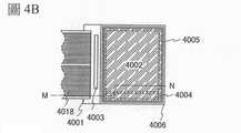
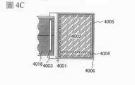
在圖4A中,以圍繞設置在基板4001上的像素部4002的方式設置密封材料4005,使用基板4006進行密封。在圖4A中,在基板4001上的與由密封材料4005圍繞的區域不同的區域中安裝有使用單晶半導體膜或多晶半導體膜形成在IC晶片或另行準備的基板上的掃描線驅動電路4004、信號線驅動電路4003。此外,藉由信號線驅動電路4003和掃描線驅動電路4004供應到像素部4002的各種信號及電位由FPC(Flexible printed circuit:撓性印刷電路)4018a及4018b供應。In FIG. 4A , a sealing
在圖4B和圖4C中,以圍繞設置在基板4001上的像素部4002和掃描線驅動電路4004的方式設置有密封材料4005。此外,在像素部4002和掃描線驅動電路4004上設置有基板4006。因此,像素部4002、掃描線驅動電路4004與顯示元件一起由基板4001、密封材料4005以及基板4006密封。在圖4B和圖4C中,在基板4001上的與由密封材料4005圍繞的區域不同的區域中安裝有使用單晶半導體膜或多晶半導體膜形成在IC晶片或另行準備的基板上的信號線驅動電路4003。在圖4B和圖4C中,藉由信號線驅動電路4003和掃描線驅動電路4004供應到像素部4002的各種信號及電位由FPC4018供應。In FIGS. 4B and 4C , a sealing
此外,圖4B和圖4C示出另行形成信號線驅動電路4003並且將該信號線驅動電路4003安裝到基板4001的例子,但是不侷限於該結構。既可以另行形成掃描線驅動電路並進行安裝,又可以僅另行形成信號線驅動電路的一部分或者掃描線驅動電路的一部分並進行安裝。4B and 4C illustrate an example in which the signal
另外,對另行形成的驅動電路的連接方法沒有特別的限制,而可以採用COG(Chip On Glass:玻璃上晶片)方法、打線接合方法、TAB(Tapc Automated Bonding:捲帶式自動接合)方法等。圖4A是藉由COG方法安裝信號線驅動電路4003、掃描線驅動電路4004的例子,圖4B是藉由COG方法安裝信號線驅動電路4003的例子,圖4C是藉由TAB方法安裝信號線驅動電路4003的例子。The connection method of the separately formed driver circuit is not particularly limited, and COG (Chip On Glass) method, wire bonding method, TAB (Tapc Automated Bonding) method, etc. can be used. 4A is an example of mounting the signal
此外,顯示裝置包括顯示元件處於密封狀態的面板和在該面板中安裝有包括控制器的IC等狀態的模組。注意,本說明書中的顯示裝置是指影像顯示裝置、顯示裝置或光源(包括照明設備)。另外,顯示裝置除了密封有顯示元件的面板之外還包括:安裝有諸如FPC或TCP的連接器的模組;在TCP的端部設置有印刷線路板的模組;或者藉由COG方法將IC(積體電路)直接安裝到顯示元件的模組。Further, the display device includes a panel in which the display element is in a sealed state, and a module in which an IC including a controller is mounted in the panel. Note that the display device in this specification refers to an image display device, a display device, or a light source (including lighting equipment). In addition, the display device has a display other than sealing.In addition to the panel showing the components, there are: a module mounted with a connector such as an FPC or a TCP; a module provided with a printed circuit board at the end of the TCP; or an IC (integrated circuit) directly mounted by the COG method to the module of the display element.
此外,設置在基板上的像素部及掃描線驅動電路具有多個電晶體,可以應用實施方式1或2所示的電晶體。In addition, the pixel portion and the scanning line driver circuit provided on the substrate have a plurality of transistors, and the transistors described in
作為設置在顯示裝置中的顯示元件,可以使用液晶元件(也稱為液晶顯示元件)、發光元件(也稱為發光顯示元件)。發光元件包括由電流或電壓控制亮度的元件,明確而言,包括無機EL(Electro Luminescence:電致發光)、有機EL等。此外,也可以應用電子墨水顯示裝置(電子紙)等的對比度因電作用而發生變化的顯示媒介。As the display element provided in the display device, a liquid crystal element (also referred to as a liquid crystal display element) and a light-emitting element (also referred to as a light-emitting display element) can be used. The light-emitting element includes an element whose luminance is controlled by current or voltage, and specifically includes inorganic EL (Electro Luminescence), organic EL, and the like. In addition, a display medium in which the contrast ratio of an electronic ink display device (electronic paper) or the like is changed by electric action can also be applied.
使用圖4A至圖5對半導體裝置的一個方式進行說明。圖5相當於沿著圖4B的線M-N的剖面圖。圖5示出將液晶元件用作顯示元件的液晶顯示裝置的例子。One form of the semiconductor device will be described with reference to FIGS. 4A to 5 . FIG. 5 corresponds to a cross-sectional view taken along line M-N of FIG. 4B . FIG. 5 shows an example of a liquid crystal display device using a liquid crystal element as a display element.
但是,只要顯示裝置以設置在像素部4002中的電晶體4010電連接到顯示元件的方式構成並該顯示元件能夠進行顯示就沒有特別的限制,而可以使用各種各樣的顯示元件。However, the display device is not particularly limited as long as the
如圖4A至圖5所示那樣,半導體裝置包括連接端子電極4015及端子電極4016,連接端子電極4015及端子電極4016藉由各向異性導電層4019電連接到FPC4018(4018a、4018b)所具有的端子。As shown in FIGS. 4A to 5 , the semiconductor device includes a
連接端子電極4015由與第一電極層4034相同的導電層形成,並且,端子電極4016由與電晶體4010、4011的源極電極層及汲極電極層相同的導電層形成。The
此外,設置在基板4001上的像素部4002、掃描線驅動電路4004具有多個電晶體,圖4A至圖5例示出像素部4002所包括的電晶體4010以及掃描線驅動電路4004所包括的電晶體4011。在圖5中,在電晶體4010、4011上設置有絕緣層4032。In addition, the
作為電晶體4010、4011,可以使用實施方式1或2所示的電晶體。在本實施方式中示出應用具有與實施方式1所示的電晶體310相同的結構的電晶體的例子。電晶體4010、4011是底閘極結構的電晶體。As the
電晶體4010、4011包括:用作用來抑制源極電極層或汲極電極層的構成元素擴散到通道的緩衝層的第一氧化物半導體層;用作通道的第二氧化物半導體層;以及設置在用作通道的氧化物半導體層與閘極絕緣層之間並用作用來防止通道與閘極絕緣層的介面劣化的緩衝層的第三氧化物半導體層。因此,電晶體4010、4011是降低有可能形成在背通道一側的介面態的影響並減少電晶體的光劣化(例如光負偏壓劣化)的可靠性高的電晶體。The
此外,可以在與驅動電路用的電晶體4011的氧化物半導體層的通道形成區域重疊的位置還設置導電層。藉由將導電層設置在與氧化物半導體層的通道形成區域重疊的位置,可以進一步降低電晶體4011的臨界電壓的變化量。此外,導電層的電位可以與電晶體4011的閘極電極層的電位相同或不同,並且,還可以將導電層用作第二閘極電極層。此外,導電層的電位可以處於浮動狀態。In addition, a conductive layer may be further provided at a position overlapping the channel formation region of the oxide semiconductor layer of the
此外,該導電層還具有遮蔽外部的電場,即不使外部的電場作用到內部(包括電晶體的電路部)的功能(尤其是,遮蔽靜電的靜電遮蔽功能)。藉由利用導電層的遮蔽功能,可以防止由於靜電等外部的電場的影響而使電晶體的電特性變動。In addition, the conductive layer also has a function of shielding an external electric field, ie, preventing an external electric field from acting on the interior (including the circuit portion of the transistor) (especially, an electrostatic shielding function of shielding static electricity). By utilizing the shielding function of the conductive layer, it is possible to prevent the electrical characteristics of the transistor from changing due to the influence of an external electric field such as static electricity.
在圖5中,液晶元件4013包括第一電極層4034、第二電極層4031以及液晶層4008。另外,以夾持液晶層4008的方式設置有用作配向膜的絕緣層4038、4033。第二電極層4031設置在基板4006一側,第一電極層4034和第二電極層4031隔著液晶層4008而層疊。In FIG. 5 , the liquid crystal element 4013 includes a
作為第一電極層4034、第二電極層4031,可以使用含有氧化鎢的銦氧化物、含有氧化鎢的銦鋅氧化物、含有氧化鈦的銦氧化物、含有氧化鈦的銦錫氧化物、銦錫氧化物、銦鋅氧化物、添加有氧化矽的銦錫氧化物、石墨烯等具有透光性的導電材料。As the
此外,第一電極層4034、第二電極層4031可以使用鎢(W)、鉬(Mo)、鋯(Zr)、鉿(Hf)、釩(V)、鈮(Nb)、鉭(Ta)、鉻(Cr)、鈷(Co)、鎳(Ni)、鈦(Ti)、鉑(Pt)、鋁(Al)、銅(Cu)、銀(Ag)等金屬、其合金或者其金屬氮化物中的一種或多種來形成。In addition, for the
此外,第一電極層4034、第二電極層4031可以使用包括導電高分子(也稱為導電聚合體)的導電組成物來形成。作為導電高分子,可以使用所謂的π電子共軛類導電高分子。例如,可以舉出聚苯胺或其衍生物、聚吡咯或其衍生物、聚噻吩或其衍生物或者由苯胺、吡咯和噻吩中的兩種以上構成的共聚物或其衍生物等。In addition, the
此外,間隔物4035是藉由對絕緣層進行選擇性地蝕刻而獲得的柱狀間隔物,並且它是為了控制液晶層4008的厚度(單元間隙(cell gap))而設置的。另外,也可以使用球狀間隔物。Further, the
當作為顯示元件使用液晶元件時,可以使用熱致液晶、鐵電液晶、反鐵電液晶等。上述液晶材料既可以是低分子化合物又可以是高分子化合物。上述液晶材料(液晶組成物)根據條件而呈現膽固醇相、近晶相、立方相、手性向列相、各向同性相等。When a liquid crystal element is used as the display element, a thermotropic liquid crystal, a ferroelectric liquid crystal, an antiferroelectric liquid crystal, or the like can be used. The above-mentioned liquid crystal material may be either a low molecular compound or a high molecular compound. The above-mentioned liquid crystal material (liquid crystal composition) exhibits a cholesteric phase, a smectic phase, a cubic phase, a chiral nematic phase, and an isotropic phase depending on conditions.
另外,也可以作為液晶層4008使用不使用配向膜的呈現藍相的液晶組成物。此時,液晶層4008與第一電極層4034和第二電極層4031接觸。藍相是液晶相的一種,是指當使膽固醇相液晶的溫度上升時即將從膽固醇相轉變到各向同性相之前出現的相。使用混合了液晶及手性試劑的液晶組成物可以呈現藍相。此外,為了擴大呈現藍相的溫度範圍,對呈現藍相的液晶組成物添加聚合性單體及聚合引發劑等,藉由進行高分子穩定化的處理來可以形成液晶層。由於呈現藍相的液晶組成物的回應時間短,並且其具有光學各向同性,所以不需要配向處理,且視角依賴性小。另外,由於不需要設置配向膜而不需要摩擦處理,因此可以防止由於摩擦處理而引起的靜電損壞,並可以降低製程中的液晶顯示裝置的故障、破損。因此,可以提高液晶顯示裝置的生產率。In addition, as the
此外,液晶材料的固有電阻為1×10⁹Ω.cm以上,較佳為1×10¹¹Ω.cm以上,更佳為1×10¹²Ω.cm以上。另外,本說明書中的固有電阻值為在20℃下測量的值。In addition, the intrinsic resistance of the liquid crystal material is 1×10⁹ Ω. cm or more, preferably 1×10¹¹ Ω. cm or more, more preferably 1×10¹² Ω. cm or more. In addition, the intrinsic resistance value in this specification is the value measured at 20 degreeC.
考慮到配置在像素部中的電晶體的洩漏電流等而以能夠在所定的期間中保持電荷的方式設定設置在液晶顯示裝置中的儲存電容器的大小。根據電晶體的關態電流(off-state current)等設定儲存電容器的大小即可。藉由使用具有本說明書所公開的氧化物半導體層的電晶體,設置具有各像素中的液晶電容的1/3以下,較佳為1/5以下的電容的儲存電容器,就足夠了。The size of the storage capacitor provided in the liquid crystal display device is set so that the electric charge can be retained for a predetermined period in consideration of leakage current of the transistor arranged in the pixel portion, and the like. The size of the storage capacitor may be set according to the off-state current of the transistor and the like. By using a transistor having the oxide semiconductor layer disclosed in this specification, it is sufficient to provide a storage capacitor having a capacitance equal to or less than 1/3, preferably 1/5 or less of the liquid crystal capacitance in each pixel.
使用本說明書所公開的氧化物半導體層的電晶體可以將截止狀態下的電流值(關態電流值)控制為低。因此,可以延長影像信號等電信號的保持時間,也可以延長寫入間隔。因此,可以降低更新工作的頻率,所以有抑制耗電量的效果。The transistor using the oxide semiconductor layer disclosed in this specification can control the current value (off-state current value) in the off state to be low. Therefore, the holding time of electric signals such as video signals can be extended, and the writing interval can also be extended. Therefore, the frequency of the update operation can be reduced, so there is an effect of suppressing power consumption.
此外,使用本說明書所公開的氧化物半導體層的電晶體可以得到較高的場效應遷移率,所以能夠進行高速驅動。例如,藉由將這種電晶體用於液晶顯示裝置,可以在同一基板上形成像素部的開關電晶體及用於驅動電路部的驅動電晶體。另外,在像素部中也藉由使用這種電晶體,可以提供高品質的影像。In addition, since a transistor using the oxide semiconductor layer disclosed in this specification can obtain a high field-effect mobility, it can be driven at a high speed. For example, by using such a transistor for a liquid crystal display device, a switching transistor for a pixel portion and a driving transistor for a driving circuit portion can be formed on the same substrate. In addition, by using such a transistor also in the pixel portion,High-quality images can be provided.
液晶顯示裝置可以採用TN(Twisted Nematic:扭曲向列)模式、IPS(In-Plane-Switching:平面內轉換)模式、FFS(Fringe Field Switching:邊緣電場轉換)模式、ASM(Axially Symmetric aligned Micro-cell:軸對稱排列微單元)模式、OCB(Optical Compensated Birefringence:光學補償彎曲)模式、FLC(Ferroelectric Liquid Crystal:鐵電性液晶)模式、AFLC(Anti Ferroelectric Liquid Crystal:反鐵電性液晶)模式等。The liquid crystal display device can adopt TN (Twisted Nematic) mode, IPS (In-Plane-Switching: in-plane switching) mode, FFS (Fringe Field Switching: fringe electric field switching) mode, ASM (Axially Symmetrically aligned Micro-cell) mode : Axisymmetric arrangement of microcells) mode, OCB (Optical Compensated Birefringence: Optical Compensation Bend) mode, FLC (Ferroelectric Liquid Crystal: Ferroelectric Liquid Crystal) mode, AFLC (Anti Ferroelectric Liquid Crystal: Antiferroelectric Liquid Crystal) mode and the like.
此外,也可以使用常黑型液晶顯示裝置,例如採用垂直配向(VA)模式的透過型液晶顯示裝置。作為垂直配向模式,可以舉出幾個例子,例如可以使用MVA(Multi-Domain Vertical Alignment:多象限垂直配向)模式、PVA(Patterned Vertical Alignment:垂直配向構型)模式、ASV(Advanced Super View:高級超視覺)模式等。另外,也可以用於VA型液晶顯示裝置。VA型液晶顯示裝置是一種控制液晶顯示面板的液晶分子的排列的方式。VA型液晶顯示裝置是在不被施加電壓時液晶分子朝向垂直於面板的方向的方式。此外,也可以使用將像素(pixel)分成幾個區域(子像素)且使分子分別倒向不同方向的被稱為多域化或多域設計的方法。In addition, a normally black type liquid crystal display device, such as a transmissive type liquid crystal display device employing a vertical alignment (VA) mode, may also be used. As the vertical alignment mode, several examples can be given. For example, MVA (Multi-Domain Vertical Alignment: multi-quadrant vertical alignment) mode, PVA (Patterned Vertical Alignment: vertical alignment configuration) mode, ASV (Advanced Super View: advanced) mode can be used Hypervision) mode, etc. In addition, it can also be used for a VA type liquid crystal display device. The VA type liquid crystal display device is a method of controlling the arrangement of liquid crystal molecules of a liquid crystal display panel. The VA type liquid crystal display device is a system in which liquid crystal molecules are oriented in a direction perpendicular to the panel when no voltage is applied. In addition, a method called multi-domain or multi-domain design in which a pixel is divided into several regions (sub-pixels) and the molecules are reversed in different directions can also be used.
此外,在顯示裝置中,適當地設置黑矩陣(遮光層)、偏振構件、相位差構件、抗反射構件等的光學構件(光學基板)等。例如,也可以使用利用偏振基板以及相位差基板的圓偏振。此外,作為光源,也可以使用背光、側光燈等。Further, in the display device, optical members (optical substrates) such as a black matrix (light shielding layer), a polarizing member, a retardation member, an antireflection member, and the like are appropriately provided. For example, it is also possible to use a polarizing substrate and a phaseCircular polarization of parallax substrates. Moreover, as a light source, a backlight, an edge light, etc. can also be used.
此外,作為像素部中的顯示方式,可以採用逐行掃描方式或隔行掃描方式等。此外,作為當進行彩色顯示時在像素中控制的顏色因素,不侷限於RGB(R表示紅色,G表示綠色,B表示藍色)這三種顏色。例如,也可以採用RGBW(W表示白色)或對RGB追加黃色(yellow)、青色(cyan)、洋紅色(magenta)等中的一種顏色以上的顏色。另外,各個色素的點的顯示區域的大小可以不同。但是,所公開的發明不侷限於彩色顯示的顯示裝置,而也可以應用於單色顯示的顯示裝置。In addition, as a display method in the pixel portion, a progressive scan method, an interlace scan method, or the like can be adopted. Further, as color factors controlled in pixels when performing color display, it is not limited to three colors of RGB (R represents red, G represents green, and B represents blue). For example, RGBW (W represents white) or one or more colors of yellow, cyan, and magenta may be added to RGB. In addition, the size of the display area of the dots of the respective dyes may be different. However, the disclosed invention is not limited to display devices of color display, but can also be applied to display devices of monochrome display.
圖11A至圖11C示出在圖5所示的顯示裝置中將用來電連接於設置在基板4006上的第二電極層4031的共同連接部(焊盤部)形成在基板4001上的例子。11A to 11C illustrate an example in which a common connection portion (pad portion) for electrically connecting to the
共同連接部配置在與用來黏合基板4001和基板4006的密封材料重疊的位置,並且藉由密封材料所包含的導電粒子與第二電極層4031電連接。或者,也可以在不與密封材料重疊的位置(像素部以外)設置共同連接部,並且,以與共同連接部重疊的方式將包括導電粒子的膏劑與密封材料另行設置,而與第二電極層4031電連接。The common connection portion is disposed at a position overlapping with the sealing material for bonding the
圖11A是共同連接部的剖面圖,圖11A相當於沿著圖11B所示的俯視圖中的線G1-G2的剖面。11A is a cross-sectional view of the common connection portion, and FIG. 11A corresponds to a cross-section taken along the line G1 - G2 in the plan view shown in FIG. 11B .
共用電位線491設置在閘極絕緣層4020上並利用與圖5所示的電晶體4010、4011的源極電極層或汲極電極層相同的材料及製程製造。The common
此外,共用電位線491由絕緣層4032覆蓋,並且絕緣層4032在與共用電位線491重疊的位置具有多個開口部。該開口部藉由與連接電晶體4010的源極電極層和汲極電極層中的一方與第一電極層4034的接觸孔相同的製程來形成。Further, the common
另外,共同電極492設置在絕緣層4032上,並利用與連接端子電極4015和像素部的第一電極層4034相同的材料及製程而形成。In addition, the
如此,可以與像素部4002的切換元件的製程共同地形成共同連接部。In this way, the common connection portion can be formed together with the manufacturing process of the switching element of the
共同電極492是與包括在密封材料中的導電粒子接觸的電極,與基板4006的第二電極層4031電連接。The
另外,如圖11C所示,共用電位線491也可以利用與電晶體4010、4011的閘極電極層相同的材料及製程而形成。In addition, as shown in FIG. 11C , the common
在圖11C所示的共同連接部中,共用電位線491設置在閘極絕緣層4020及絕緣層4032的下層中,並且閘極絕緣層4020及絕緣層4032在與共用電位線491重疊的位置具有多個開口部。該開口部在藉由與連接電晶體4010的源極電極層和汲極電極層中的一方與第一電極層4034的接觸孔相同的製程對絕緣層4032進行蝕刻之後,對閘極絕緣層4020選擇性地進行蝕刻來形成。In the common connection portion shown in FIG. 11C , the common
此外,作為顯示裝置所包括的顯示元件,可以應用利用電致發光的發光元件。利用電致發光的發光元件根據發光材料是有機化合物還是無機化合物被區分,一般地,前者被稱為有機EL元件,而後者被稱為無機EL元件。In addition, as the display element included in the display device, it is possible to apply theLight-emitting element using electroluminescence. Light-emitting elements utilizing electroluminescence are classified according to whether the light-emitting material is an organic compound or an inorganic compound, and generally, the former is called an organic EL element and the latter is called an inorganic EL element.
在有機EL元件中,藉由對發光元件施加電壓,電子及電洞分別從一對電極注入到包括發光性有機化合物的層,於是電流流過。並且,藉由這些載流子(電子及電洞)的重新結合,發光性有機化合物形成激發態,當從該激發態回到基態時發光。由於這種機制,這種發光元件被稱為電流激發型發光元件。在本實施方式中,示出作為發光元件使用有機EL元件的例子。In the organic EL element, by applying a voltage to the light-emitting element, electrons and holes are injected from a pair of electrodes into a layer including a light-emitting organic compound, respectively, and current flows. Then, by the recombination of these carriers (electrons and holes), the light-emitting organic compound forms an excited state, and emits light when returning from the excited state to the ground state. Due to this mechanism, such a light-emitting element is called a current-excitation type light-emitting element. In this embodiment mode, an example in which an organic EL element is used as a light-emitting element is shown.
無機EL元件根據其元件結構而分類為分散型無機EL元件和薄膜型無機EL元件。分散型無機EL元件具有發光材料的粒子分散在黏合劑中的發光層,其發光機制是利用施體能階和受體能階的施體-受體重新結合型發光。薄膜型無機EL元件具有發光層夾在介電層之間且該介電層由電極夾住的結構,其發光機制是利用金屬離子的內殼層電子躍遷的定域型發光(localized type light emission)。在此,作為發光元件使用有機EL元件進行說明。Inorganic EL elements are classified into dispersion-type inorganic EL elements and thin-film-type inorganic EL elements according to their element structures. The dispersion-type inorganic EL element has a light-emitting layer in which particles of a light-emitting material are dispersed in a binder, and its light-emitting mechanism is donor-acceptor recombination type light emission using a donor level and an acceptor level. The thin-film inorganic EL element has a structure in which a light-emitting layer is sandwiched between dielectric layers and the dielectric layer is sandwiched by electrodes. ). Here, an organic EL element is used as a light-emitting element for description.
為了取出發光,使發光元件的一對電極中的至少一個具有透光性即可。並且,在基板上形成電晶體及發光元件,作為發光元件,有:從與基板相反一側的表面取出發光的頂部發射結構的發光元件;從基板一側的表面取出發光的底部發射結構的發光元件;以及從基板一側及與基板相反一側的表面取出發光的雙面發射結構的發光元件,可以應用上述任一種發射結構的發光元件。In order to extract light emission, at least one of the pair of electrodes of the light-emitting element may be made translucent. In addition, a transistor and a light-emitting element are formed on the substrate. As the light-emitting element, there are: a light-emitting element of a top-emission structure that emits light from the surface opposite to the substrate; a light-emitting element of a bottom-emission structure that emits light from the surface of the substrate side elements; and light-emitting elements with a double-sided emission structure that emit light from the surface of the substrate side and the opposite side of the substrate, which can beA light-emitting element with any of the above-mentioned emission structures is applied.
圖6A、圖6B及圖13示出作為顯示元件使用發光元件的發光裝置的例子。6A , 6B and 13 show an example of a light-emitting device using a light-emitting element as a display element.
圖6A是發光裝置的剖面圖,圖6A中的以點劃線S1-T1、S2-T2及S3-T3切斷的剖面相當於圖6B。另外,圖13相當於圖6A中的以點劃線S4-T4切斷的剖面圖。另外,在圖6A的平面圖中,省略電致發光層542及第二電極層543而未圖示。FIG. 6A is a cross-sectional view of the light-emitting device, and the cross-sections cut along the dot-and-dash lines S1-T1, S2-T2, and S3-T3 in FIG. 6A correspond to FIG. 6B. In addition, FIG. 13 corresponds to the cross-sectional view cut|disconnected by the dashed-dotted line S4-T4 in FIG. 6A. In addition, in the plan view of FIG. 6A , the
圖6A和圖6B所示的發光裝置在基板500上具有電晶體510、電容元件520、佈線層交叉部530,電晶體510與發光元件540電連接。另外,圖6A和圖6B示出經過基板500從發光元件540取光的底面發射型結構的發光裝置。The light-emitting device shown in FIGS. 6A and 6B includes a
作為電晶體510,可以使用實施方式1或2所示的電晶體。在本實施方式中示出應用具有與實施方式2所示的電晶體330相同的結構的電晶體的例子。電晶體510是底閘極結構的電晶體。As the
電晶體510包括:閘極電極層511a、閘極電極層511b;包括閘極絕緣層502a、閘極絕緣層502b及閘極絕緣層502c的閘極絕緣層502;包括氧化物半導體層512b及氧化物半導體層512a的氧化物半導體疊層512;以及用作源極電極層或汲極電極層的導電層513a、導電層513b。另外,在電晶體510上形成有絕緣層525。The
電容元件520包括:導電層521a、導電層521b;閘極絕緣層502;包括氧化物半導體層522b及氧化物半導體層522a的氧化物半導體疊層522;以及導電層523。並且,以由導電層521a、導電層521b以及導電層523夾著閘極絕緣層502及氧化物半導體疊層522的結構來形成電容器。The
佈線層交叉部530是閘極電極層511a、閘極電極層511b和導電層533的交叉部,並且閘極電極層511a、閘極電極層511b和導電層533隔著閘極絕緣層502交叉。The
在本實施方式中,作為閘極電極層511a及導電層521a使用30nm厚的鈦膜,作為閘極電極層511b及導電層521b使用200nm厚的銅膜。因此,閘極電極層具有鈦膜和銅膜的疊層結構。In the present embodiment, a titanium film having a thickness of 30 nm is used as the
電晶體510包括:用作通道的氧化物半導體層512b;以及用作用來抑制導電層513a及導電層513b的構成元素擴散到通道的緩衝層的氧化物半導體層512a。因此,電晶體510是降低有可能形成在背通道一側的介面態的影響的可靠性高的電晶體。The
此外,電晶體510包括:用作閘極絕緣層502c的氨的含量少的用作阻擋銅的障壁膜的含有氮的矽膜;用作閘極絕緣層502a的厚度大(例如,300nm厚)且缺陷少的含有氮的矽膜;以及用作閘極絕緣層502b的氫濃度低的含有氮的矽膜。藉由採用上述結構,可以改善電晶體510的電特性,還可以防止電晶體510的靜電破壞。由此,可以以高良率地製造高可靠性的半導體裝置。In addition, the
在電晶體510、電容元件520、佈線層交叉部530上形成有層間絕緣層504,並且在層間絕緣層504上的與發光元件540重疊的區域設置有彩色濾光層505。在層間絕緣層504及彩色濾光層505上設置有用作平坦化絕緣層的絕緣層506。An interlayer insulating
在絕緣層506上設置有包含依次層疊第一電極層541、電致發光層542、第二電極層543的疊層結構的發光元件540。藉由在到達導電層513a且形成在絕緣層506及層間絕緣層504中的開口中第一電極層541與導電層513a接觸,發光元件540與電晶體510電連接。此外,以覆蓋第一電極層541的一部分及該開口的方式設置有隔壁507。On the insulating
作為絕緣層506可以使用1500nm厚的感光性丙烯酸膜,作為隔壁507可以使用1500nm厚的感光性聚醯亞胺膜。As the insulating
作為彩色濾光層505,例如可以使用彩色的透光樹脂。作為彩色透光樹脂,可以使用感光性有機樹脂、非感光性有機樹脂。當使用感光性有機樹脂層時,可以減少光阻遮罩數量而簡化製程,所以是較佳的。As the
彩色是指如黑色、灰色和白色等無彩色以外的顏色。彩色濾光層由只使彩色的光透過的材料形成。至於彩色,可以使用紅色、綠色、藍色等。另外,還可以使用青色(cyan)、洋紅色(magenta)、黃色(yellow)等。只使彩色的光透過意味著:透過彩色濾光層的光在其彩色的光的波長中具有峰值。關於彩色濾光層的厚度,可以根據所包含的著色材料的濃度與光的透過率的關係適當地控制為最適合的膜厚度即可。例如,將彩色濾光層505的厚度設定為1500nm以上且2000nm以下,即可。Color refers to colors other than achromatic colors such as black, gray and white. The color filter layer is formed of a material that transmits only colored light. As for the color, red, green, blue, etc. can be used. In addition, cyan, magenta, yellow, or the like can also be used. Passing only colored light means: the light passing through the color filter layer is in its colored lighthas a peak at the wavelength of . The thickness of the color filter layer may be appropriately controlled to an optimum film thickness according to the relationship between the concentration of the coloring material contained and the transmittance of light. For example, the thickness of the
隔壁507使用有機絕緣材料或無機絕緣材料形成。尤其是,較佳為使用感光樹脂材料,在第一電極層541上形成開口部,並且將該開口部的側壁形成為具有連續曲率的傾斜面。The
電致發光層542可以使用一個層構成,也可以使用多個層的疊層構成。The
為了防止氧、氫、水分、二氧化碳等侵入到發光元件540中,也可以在第二電極層543及隔壁507上形成保護膜。作為保護膜,可以形成氮化矽膜、氮氧化矽膜、DLC膜等。A protective film may be formed on the
另外,為了不使氧、氫、水分、二氧化碳等侵入到發光元件540,也可以藉由蒸鍍法形成覆蓋發光元件540的包含有機化合物的層。In addition, in order to prevent oxygen, hydrogen, moisture, carbon dioxide, etc. from entering the light-emitting
另外,如果需要,也可以在發光元件的射出表面上適當地設置諸如偏光板或者圓偏光板(包括橢圓偏光板)、相位差板(λ/4板,λ/2板)、彩色濾光片等的光學薄膜。此外,也可以在偏光板或圓偏光板上設置防反射膜。例如,可以進行抗眩光處理,該處理是利用表面的凹凸來擴散反射光而可以降低眩光的處理。In addition, if necessary, a polarizing plate or a circular polarizing plate (including an elliptical polarizing plate), a retardation plate (λ/4 plate, λ/2 plate), a color filter can also be appropriately provided on the exit surface of the light-emitting element. and other optical films. In addition, an antireflection film may be provided on a polarizing plate or a circular polarizing plate. For example, anti-glare treatment, which can reduce glare by diffusing reflected light by the unevenness of the surface, can be performed.
此外,作為顯示裝置,也可以提供驅動電子墨水的電子紙。電子紙也稱為電泳顯示裝置(電泳顯示器),並具有如下優點:與紙同樣的易讀性;其耗電量比其他顯示裝置的耗電量低;形狀薄且輕。In addition, as a display device, electricity for driving electronic ink can also be provided.Sub paper. Electronic paper is also called an electrophoretic display device (electrophoretic display), and has the following advantages: the same legibility as paper; its power consumption is lower than that of other display devices; its shape is thin and light.
作為電泳顯示裝置,可以有各種各樣的形式,但是它是包括具有正電荷的第一粒子和具有負電荷的第二粒子的多個微膠囊分散在溶劑中,並且,藉由對微膠囊施加電場,使微膠囊中的粒子向彼此相反的方向移動,以只顯示集合在一側的粒子的顏色的裝置。另外,第一粒子或第二粒子包括染料,當沒有電場時不移動。此外,第一粒子的顏色和第二粒子的顏色不同(包括無色)。As the electrophoretic display device, various forms are possible, but it is one in which a plurality of microcapsules including first particles having a positive charge and second particles having a negative charge are dispersed in a solvent, and by applying An electric field that causes the particles in the microcapsules to move in opposite directions to each other, so that only the colors of the particles gathered on one side are displayed. Additionally, either the first particle or the second particle includes a dye and does not move in the absence of an electric field. In addition, the color of the first particles and the color of the second particles are different (including colorless).
分散有上述微囊的溶劑被稱為電子墨水。還可以藉由使用彩色濾光片、具有色素的粒子來進行彩色顯示。The solvent in which the above-mentioned microcapsules are dispersed is called electronic ink. Color display can also be performed by using color filters and particles with pigments.
另外,作為用作平坦化絕緣層的絕緣層506,可以使用丙烯酸樹脂、聚醯亞胺樹脂、苯並環丁烯類樹脂、聚醯胺樹脂、環氧樹脂等具有耐熱性的有機材料。此外,除了上述有機材料以外,還可以使用矽氧烷類樹脂、PSG(磷矽玻璃)、BPSG(硼磷矽玻璃)等低介電常數材料(low-k材料)。另外,也可以藉由層疊多個由上述材料形成的絕緣層形成絕緣層506。In addition, as the insulating
對絕緣層506的形成方法沒有特別的限制,可以根據其材料利用濺射法、旋塗法、浸漬法、噴塗法、液滴噴射法(噴墨法等)、印刷法(絲網印刷、膠版印刷等)等。The formation method of the insulating
作為第一電極層541、第二電極層543,可以應用與圖5所示的顯示裝置的第一電極層4034、第二電極層4031相同的材料。As the
在本實施方式中,圖6A和圖6B所示的發光裝置是底部發射型,所以第一電極層541具有透光性,第二電極層543具有反射性。因此,當作為第一電極層541使用金屬膜時,將該金屬膜的厚度形成得薄到具有透光性的程度。當作為第二電極層543使用具有透過性的導電層時,可以層疊具有反射性的導電層。In this embodiment mode, the light-emitting device shown in FIG. 6A and FIG. 6B is a bottom emission type, so the
此外,也可以設置驅動電路保護用的保護電路。保護電路較佳為使用非線性元件構成。In addition, a protection circuit for driving circuit protection may be provided. The protection circuit is preferably constructed using nonlinear elements.
如上所述,藉由應用實施方式1或2所示的電晶體,可以提供具有各種各樣的功能的半導體裝置。As described above, by applying the transistor described in
本實施方式所示的結構、方法等可以與其他實施方式所示的結構、方法等適當地組合而實施。The structures, methods, and the like shown in this embodiment can be implemented in combination with structures, methods, and the like shown in other embodiments as appropriate.
藉由使用實施方式1或2所示的電晶體,可以製造具有讀取目標物的資訊的影像感測器功能的半導體裝置。By using the transistor shown in
圖7A示出具有影像感測器功能的半導體裝置的一個例子。圖7A是光電感測器的等效電路,而圖7B是示出光電感測器的一部分的剖面圖。FIG. 7A shows an example of a semiconductor device having an image sensor function. FIG. 7A is an equivalent circuit of the photoelectric sensor, and FIG. 7B is a cross-sectional view showing a part of the photoelectric sensor.
光電二極體602的一個電極電連接到光電二極體重設信號線658,而光電二極體602的另一個電極電連接到電晶體640的閘極。電晶體640的源極和汲極中的一個電連接到光電感測器基準信號線672,而電晶體640的源極和汲極中的另一個電連接到電晶體656的源極和汲極中的一個。電晶體656的閘極電連接到閘極信號線659,電晶體656的源極和汲極中的另一個電連接到光電感測器輸出信號線671。One electrode of the
注意,在本說明書的電路圖中,為了使使用氧化物半導體層的電晶體一目了然,將使用氧化物半導體層的電晶體的符號表示為“OS”。在圖7A中,電晶體640、656可以應用實施方式1或2所示的電晶體,是使用氧化物半導體層的電晶體。在本實施方式中示出應用具有與實施方式1所示的電晶體320相同的結構的電晶體的例子。電晶體640是底閘極結構的電晶體。Note that, in the circuit diagrams of this specification, in order to make the transistor using the oxide semiconductor layer clear at a glance, the symbol of the transistor using the oxide semiconductor layer is denoted as “OS”. In FIG. 7A , the
圖7B是示出光電感測器中的光電二極體602和電晶體640的剖面圖,其中在具有絕緣表面的基板601(元件基板)上設置有用作感測器的光電二極體602和電晶體640。藉由使用黏合層608,在光電二極體602和電晶體640上設置有基板613。7B is a cross-sectional view showing the
在電晶體640上設置有絕緣層632、層間絕緣層633以及層間絕緣層634。光電二極體602具有:形成在層間絕緣層633上的電極層641b;在電極層641b上依次層疊的第一半導體膜606a、第二半導體膜606b、第三半導體膜606c;設置在層間絕緣層634上的藉由第一半導體膜至第三半導體膜與電極層641b電連接的電極層642;以及設置在與電極層641b同樣的層中的與電極層642電連接的電極層641a。An insulating
電極層641b與形成在層間絕緣層634中的導電層643電連接,並且電極層642藉由電極層641a與導電層645電連接。導電層645與電晶體640的閘極電極層電連接,並且光電二極體602與電晶體640電連接。The
在此,例示出一種pin型光電二極體,其中層疊用作第一半導體膜606a的具有p型導電型的半導體膜、用作第二半導體膜606b的高電阻的半導體膜(i型半導體膜)、用作第三半導體膜606c的具有n型導電型的半導體膜。Here, a pin-type photodiode is exemplified in which a semiconductor film having a p-type conductivity type serving as the
第一半導體膜606a是p型半導體膜,而可以由包含賦予p型的雜質元素的非晶矽膜形成。使用包含屬於週期表中的第13族的雜質元素(例如,硼(B))的半導體材料氣體藉由電漿CVD法來形成第一半導體膜606a。作為半導體材料氣體,可以使用矽烷(SiH4)。另外,可以使用Si2H6、SiH2Cl2、SiHCl3、SiCl4、SiF4等。另外,也可以使用如下方法:在形成不包含雜質元素的非晶矽膜之後,使用擴散法或離子植入法將雜質元素導入到該非晶矽膜。較佳為在使用離子植入法等導入雜質元素之後進行加熱等來使雜質元素擴散。在此情況下,作為形成非晶矽膜的方法,可以使用LPCVD法、氣相生長法或濺射法等。較佳為將第一半導體膜606a的厚度設定為10nm以上且50nm以下。The
第二半導體膜606b是i型半導體膜(本質半導體膜),由非晶矽膜形成。為了形成第二半導體膜606b,藉由電漿CVD法使用半導體材料氣體來形成非晶矽膜。作為半導體材料氣體,可以使用矽烷(SiH4)。或者,也可以使用Si2H6、SiH2Cl2、SiHCl3、SiCl4或SiF4等。也可以藉由LPCVD法、氣相生長法、濺射法等形成第二半導體膜606b。較佳為將第二半導體膜606b的厚度設定為200nm以上且1000nm以下。The
第三半導體膜606c是n型半導體膜,由包含賦予n型的雜質元素的非晶矽膜形成。使用包含屬於週期表中的第15族的雜質元素(例如,磷(P))的半導體材料氣體藉由電漿CVD法形成第三半導體膜606c。作為半導體材料氣體,可以使用矽烷(SiH4)。或者,也可以使用Si2H6、SiH2Cl2、SiHCl3、SiCl4或SiF4等。另外,也可以使用如下方法:在形成不包含雜質元素的非晶矽膜之後,使用擴散法或離子植入法將雜質元素導入到該非晶矽膜。較佳為在使用離子植入法等導入雜質元素之後進行加熱等來使雜質元素擴散。在此情況下,作為形成非晶矽膜的方法,可以使用LPCVD法、氣相生長法或濺射法等。較佳為將第三半導體膜606c的厚度設定為20nm以上且200nm以下。The
此外,第一半導體膜606a、第二半導體膜606b以及第三半導體膜606c也可以不使用非晶半導體形成,而使用多晶半導體或微晶半導體(Semi Amorphous Semiconductor:SAS)形成。In addition, the
此外,由於藉由光電效應生成的電洞的遷移率低於電子的遷移率,因此當將p型半導體膜側的表面用作光接收面時,pin型光電二極體具有較好的特性。在此示出將光電二極體602從形成有pin型光電二極體的基板601的面接收的光轉換為電信號的例子。此外,來自其導電型與用作光接收面的半導體膜一側相反的半導體膜一側的光是干擾光,因此,電極層較佳為使用具有遮光性的導電層。另外,也可以將n型半導體膜一側的表面用作光接收面。In addition, since the mobility of holes generated by the photoelectric effect is lower than that of electricTherefore, when the surface on the p-type semiconductor film side is used as a light-receiving surface, the pin-type photodiode has better characteristics. Here, an example of converting light received by the
電晶體640包括:用作用來抑制源極電極層或汲極電極層的構成元素擴散到通道的緩衝層的第一氧化物半導體層;用作通道的第二氧化物半導體層;以及設置在用作通道的氧化物半導體層與閘極絕緣層631之間並用作用來防止通道與閘極絕緣層631的介面劣化的緩衝層的第三氧化物半導體層。因此,電晶體640是降低有可能形成在背通道一側的介面態的影響並減少電晶體的光劣化(例如光負偏壓劣化)的可靠性高的電晶體。The
藉由使用絕緣材料且根據其材料使用濺射法、電漿CVD法、旋塗法、浸漬法、噴塗法、液滴噴射法(噴墨法等)、印刷法(絲網印刷、膠版印刷)等,來可以形成絕緣層632、層間絕緣層633、634。By using an insulating material and depending on its material, a sputtering method, a plasma CVD method, a spin coating method, a dipping method, a spraying method, a droplet ejection method (inkjet method, etc.), a printing method (screen printing, offset printing) etc., the insulating
作為層間絕緣層633、634,較佳為採用用來減少表面凹凸的用作平坦化絕緣層的絕緣層。作為層間絕緣層633、634,例如可以使用聚醯亞胺樹脂、丙烯酸樹脂、苯並環丁烯類樹脂、聚醯胺樹脂、環氧樹脂等具有耐熱性的有機絕緣材料。此外,除了上述有機絕緣材料以外,還可以使用低介電常數材料(low-k材料)、矽氧烷類樹脂、PSG(磷矽玻璃)、BPSG(硼磷矽玻璃)等的單層或疊層。As the
藉由檢測入射到光電二極體602的光,可以讀取檢測目標的資訊。另外,在讀取檢測目標的資訊時,可以使用背光等的光源。By detecting the light incident on the
本實施方式所示的結構、方法等可以與其他實施方式所示的結構、方法等適當地組合而實施。The structures, methods, and the like shown in this embodiment can be implemented in combination with structures, methods, and the like shown in other embodiments as appropriate.
本說明書所公開的半導體裝置可以應用於各種電子裝置(也包括遊戲機)。作為電子裝置,可以舉出電視機(也稱為電視或電視接收機)、用於電腦等的顯示器、數位相機、數位攝影機、數位相框、行動電話機、可攜式遊戲機、可攜式資訊終端、音頻再生裝置、遊戲機(彈珠機(pachinko machine)或投幣機(slot machine)等)、外殼遊戲機。圖8A至圖8C示出上述電子裝置的具體例子。The semiconductor device disclosed in this specification can be applied to various electronic devices (including game machines). Examples of electronic devices include televisions (also referred to as televisions or television receivers), monitors for computers, digital cameras, digital video cameras, digital photo frames, mobile phones, portable game consoles, and portable information terminals. , audio reproduction device, game machine (pachinko machine or slot machine, etc.), shell game machine. 8A to 8C illustrate specific examples of the above-described electronic device.
圖8A示出具有顯示部的桌子9000。在桌子9000中,外殼9001組裝有顯示部9003,利用顯示部9003可以顯示影像。另外,示出利用四個桌腿9002支撐外殼9001的結構。另外,外殼9001具有用於供應電力的電源供應線9005。FIG. 8A shows a table 9000 having a display portion. In the table 9000, a
可以將上述實施方式中任一個所示的半導體裝置用於顯示部9003,由此可以對電子裝置賦予高可靠性。The semiconductor device described in any of the above-mentioned embodiments can be used forThe
顯示部9003具有觸屏輸入功能,藉由用手指等按觸顯示於桌子9000的顯示部9003中的顯示按鈕9004來可以進行屏面操作或資訊輸入,並且顯示部9003也可以用作如下控制裝置,即藉由使其具有能夠與其他家電產品進行通信的功能或能夠控制其他家電產品的功能,而藉由屏面操作控制其他家電產品。例如,藉由使用實施方式3所示的具有影像感測器功能的半導體裝置,可以使顯示部9003具有觸屏輸入功能。The
另外,利用設置於外殼9001的鉸鏈也可以將顯示部9003的屏面以垂直於地板的方式立起來,從而也可以將桌子用作電視機。雖然當在小房間裏設置大屏面的電視機時自由使用的空間變小,但是若在桌子內安裝有顯示部則可以有效地利用房間的空間。In addition, the screen of the
圖8B示出電視機9100的一個例子。在電視機9100中,外殼9101組裝有顯示部9103,並且利用顯示部9103可以顯示影像。此外,在此示出利用支架9105支撐外殼9101的結構。FIG. 8B shows an example of the
藉由利用外殼9101所具備的操作開關、另外提供的遙控器9110,可以進行電視機9100的操作。藉由利用遙控器9110所具備的操作鍵9109,可以進行頻道及音量的操作,並可以對在顯示部9103上顯示的影像進行操作。此外,也可以採用在遙控器9110中設置顯示從該遙控器9110輸出的資訊的顯示部9107的結構。The
圖8B所示的電視機9100具備接收機及數據機等。電視機9100可以利用接收機接收一般的電視廣播。再者,電視機9100藉由數據機連接到有線或無線方式的通信網路,也可以進行單向(從發送者到接收者)或雙向(發送者和接收者之間或接收者之間等)的資訊通信。The
可以將上述實施方式中任一個所示的半導體裝置用於顯示部9103、9107,而能夠對電視機及遙控器賦予高可靠性。The semiconductor device described in any of the above-described embodiments can be used for the
圖8C示出電腦,該電腦包括主體9201、外殼9202、顯示部9203、鍵盤9204、外部連接埠9205、指向裝置9206等。8C shows a computer, which includes a
可以將上述實施方式中任一個所示的半導體裝置用於顯示部9203,而能夠對電腦賦予高可靠性。The semiconductor device described in any of the above-described embodiments can be used for the
圖9A和圖9B是能夠折疊的平板終端。圖9A是打開的狀態,並且平板終端包括外殼9630、顯示部9631a、顯示部9631b、顯示模式切換開關9034、電源開關9035、省電模式切換開關9036、卡子9033以及操作開關9038。9A and 9B are tablet terminals that can be folded. 9A is an open state, and the tablet terminal includes a
可以將上述實施方式中任一個所示的半導體裝置用於顯示部9631a、9631b,而能夠實現可靠性高的平板終端。The semiconductor device described in any of the above-described embodiments can be used for the
在顯示部9631a中,可以將其一部分用作觸摸屏的區域9632a,並且可以藉由按觸所顯示的操作鍵9638來輸入資料。此外,作為一個例子在此示出:顯示部9631a的一半只具有顯示的功能,並且另一半具有觸摸屏的功能,但是不侷限於該結構。也可以採用顯示部9631a的全部區域具有觸摸屏的功能的結構。例如,可以使顯示部9631a的整個面顯示鍵盤按鈕來將其用作觸摸屏,並且將顯示部9631b用作顯示幕面。In the
此外,顯示部9631b也與顯示部9631a同樣,可以將其一部分用作觸摸屏的區域9632b。此外,藉由使用手指或觸控筆等按觸觸摸屏的顯示鍵盤顯示切換按鈕9639的位置,可以在顯示部9631b顯示鍵盤按鈕。In addition, the
此外,也可以對觸摸屏的區域9632a和觸摸屏的區域9632b同時進行按觸輸入。In addition, the touch input may be simultaneously performed on the
另外,顯示模式切換開關9034能夠進行豎屏顯示和橫屏顯示等顯示的方向的切換以及黑白顯示或彩色顯示等的切換等。根據內置於平板終端中的光感測器所檢測的使用時的外光的光量,省電模式切換開關9036可以將顯示的亮度設定為最適合的亮度。平板終端除了光感測器以外還可以內置陀螺儀和加速度感測器等檢測傾斜度的感測器等的其他檢測裝置。In addition, the display
此外,圖9A示出顯示部9631b的顯示面積與顯示部9631a的顯示面積相同的例子,但是不侷限於此,一方的尺寸和另一方的尺寸可以不同,並且它們的顯示品質也可以不同。例如顯示部9631a和顯示部9631b中的一方可以進行比另一方更高精細的顯示。9A shows an example in which the display area of the
圖9B是合上的狀態,並且平板終端包括外殼9630、太陽能電池9633、充放電控制電路9634。此外,在圖9B中,作為充放電控制電路9634的一個例子示出具有電池9635和DCDC轉換器9636的結構。9B is a closed state, and the tablet terminal includes a
此外,平板終端可以折疊,因此不使用時可以合上外殼9630。因此,可以保護顯示部9631a和顯示部9631b,而可以提供一種具有良好的耐久性且從長期使用的觀點來看具有良好的可靠性的平板終端。Additionally, the tablet terminal can be folded so that the
此外,圖9A和圖9B所示的平板終端還可以具有如下功能:顯示各種各樣的資訊(靜態影像、動態影像、文字影像等);將日曆、日期或時刻等顯示在顯示部上;對顯示在顯示部上的資訊進行操作或編輯的觸摸輸入;藉由各種各樣的軟體(程式)控制處理等。In addition, the tablet terminal shown in FIG. 9A and FIG. 9B may also have the following functions: display various information (still images, moving images, text images, etc.); display the calendar, date or time, etc. on the display unit; Touch input to operate or edit the information displayed on the display unit; control processing by various software (programs), etc.
藉由利用安裝在平板終端的表面上的太陽能電池9633,可以將電力供應到觸摸屏、顯示部或影像信號處理部等。注意,太陽能電池9633可以設置在外殼9630的一面或兩面,因此可以進行高效的電池9635的充電。另外,當作為電池9635使用鋰離子電池時,有可以實現小型化等的優點。By using the
另外,參照圖9C所示的方塊圖對圖9B所示的充放電控制電路9634的結構和工作進行說明。圖9C示出太陽能電池9633、電池9635、DCDC轉換器9636、轉換器9637、開關SW1至SW3以及顯示部9631,電池9635、DCDC轉換器9636、轉換器9637、開關SW1至SW3對應於圖9B所示的充放電控制電路9634。In addition, the configuration and operation of the charge/
首先,說明在利用外光使太陽能電池9633發電時的工作的例子。使用DCDC轉換器9636對太陽能電池所產生的電力進行升壓或降壓以使它成為用來對電池9635進行充電的電壓。並且,當利用來自太陽能電池9633的電力使顯示部9631工作時使開關SW1導通,並且,利用轉換器9637將其升壓或降壓到顯示部9631所需要的電壓。另外,當不進行顯示部9631中的顯示時,可以採用使SW1截止且使SW2導通來對電池9635進行充電的結構。First, when the
注意,作為發電單元的一個例子示出太陽能電池9633,但是不侷限於此,也可以使用壓電元件(piezoelectric element)或熱電轉換元件(珀耳帖元件(Peltier element))等其他發電單元進行電池9635的充電。例如,也可以使用以無線(不接觸)的方式能夠收發電力來進行充電的無線電力傳輸模組或組合其他充電方法進行充電。Note that the
本實施方式所示的結構、方法等可以與其他實施方式所示的結構、方法等適當地組合而實施。The structures, methods, and the like shown in this embodiment can be implemented in combination with structures, methods, and the like shown in other embodiments as appropriate.
在本實施例中,示出在層疊有氧化物半導體層的電晶體中對各氧化物半導體層所含有的源極電極層或汲極電極層的構成元素的濃度進行測量的結果。明確而言,示出作為源極電極層及汲極電極層形成包括銅膜的電極層並對各氧化物半導體層中的銅的濃度進行測量的結果。利用SSDP-SIMS(Substrate Side Depth Profile Secondary Ion Mass Spectrometry)測量銅濃度。This example shows the results of measuring the concentration of the constituent elements of the source electrode layer or the drain electrode layer contained in each oxide semiconductor layer in a transistor in which oxide semiconductor layers are stacked. Specifically, the results of measuring the concentration of copper in each oxide semiconductor layer by forming an electrode layer including a copper film as the source electrode layer and the drain electrode layer are shown. Using SSDP-SIMS (Substrate Side Depth Profile Secondary IonMass Spectrometry) to measure copper concentration.
以下說明在本實施例中用於測量的電晶體的製造方法。在本實施例中,製造具有與實施方式1的電晶體300相同的結構的電晶體。以下,使用與電晶體300相同的符號進行說明。A method of manufacturing the transistor used for measurement in this embodiment will be described below. In this example, a transistor having the same structure as that of the
首先,在基板400上作為閘極電極層402形成厚度為100nm的鎢膜。First, a tungsten film having a thickness of 100 nm is formed on the
接著,作為覆蓋閘極電極層402的閘極絕緣層404,利用電漿CVD法連續地形成50nm厚的氮化矽膜和200nm厚的氧氮化矽膜。Next, as the
藉由將電漿CVD設備的處理室的壓力控制為60Pa,用27.12MHz的高頻電源供應150W的功率,將基板溫度設定為350℃,供應矽烷和氮的混合氣體(SiH4:N2=50sccm:5000sccm),來形成氮化矽膜。另外,該電漿CVD設備是電極面積為6000cm2的平行平板型電漿CVD設備。另外,藉由在相同的處理室內將壓力設定為40Pa,在維持高頻電源的功率及基板溫度的狀態下供應矽烷和一氧化二氮的混合氣體(SiH4:N2O=20sccm:3000sccm),來形成氧氮化矽膜。By controlling the pressure of the processing chamber of the plasma CVD apparatus to 60 Pa, supplying a power of 150 W with a high-frequency power supply of 27.12 MHz, setting the substrate temperature to 350° C., and supplying a mixed gas of silane and nitrogen (SiH4 : N2 = 50sccm: 5000sccm) to form a silicon nitride film. In addition, this plasma CVD apparatus is a parallel plate type plasma CVD apparatuswith an electrode area of 6000 cm 2 . In addition, by setting the pressure to 40 Pa in the same processing chamber, a mixed gas of silane and nitrous oxide (SiH4 : N2 O=20 sccm: 3000 sccm) was supplied while maintaining the power of the high-frequency power supply and the temperature of the substrate. , to form a silicon oxynitride film.
接著,藉由利用使用In:Ga:Zn=1:1:1[原子數比]的金屬氧化物靶材的濺射法,在閘極絕緣層404上形成厚度為10nm的氧化物半導體層408b。成膜條件為如下:氧50%氛圍下;壓力為0.6Pa;功率為5kW;基板溫度為170℃。Next, an
然後,藉由利用使用In:Ga:Zn=3:1:2[原子數比]的金屬氧化物靶材的濺射法,在氧化物半導體層408b上形成厚度為30nm的氧化物半導體層408a。成膜條件為如下:氧50%氛圍下;壓力為0.6Pa;功率為5kW;基板溫度為170℃。Then, an
在將氧化物半導體層408a及氧化物半導體層408b加工為島狀的氧化物半導體疊層408之後,在氮氛圍下以450℃的溫度對氧化物半導體疊層408進行1小時的加熱處理,然後在氮及氧氛圍下以450℃的溫度對氧化物半導體疊層408進行1小時的加熱處理。After the
接著,形成接觸於氧化物半導體疊層408的源極電極層410a及汲極電極層410b。Next, the
在本實施例中,藉由在閘極絕緣層404及氧化物半導體疊層408上層疊厚度為35nm的鈦膜和厚度為200nm的銅膜並對該鈦膜及銅膜的一部分選擇性地進行蝕刻,來形成源極電極層410a及汲極電極層410b。In the present embodiment, a titanium film having a thickness of 35 nm and a copper film having a thickness of 200 nm are stacked on the
然後,作為覆蓋氧化物半導體疊層408、源極電極層410a及汲極電極層410b的絕緣層412,藉由電漿CVD法形成厚度為400nm的氧氮化矽膜。Then, as the insulating
藉由將電漿CVD設備的處理室的壓力控制為200Pa,用27.12MHz的高頻電源供應1500W的功率,將基板溫度設定為220℃,供應矽烷和一氧化二氮的混合氣體(SiH4:N2O=160sccm:4000sccm),來形成氧氮化矽膜。By controlling the pressure of the processing chamber of the plasma CVD equipment to 200Pa, supplying a power of 1500W with a high-frequency power supply of 27.12MHz, setting the substrate temperature to 220°C, and supplying a mixed gas of silane and nitrous oxide (SiH4 : N2 O = 160 sccm: 4000 sccm) to form a silicon oxynitride film.
在氮及氧氛圍下以300℃的溫度進行1小時的加熱處理,然後作為平坦化膜形成厚度為1.5μm的丙烯酸樹脂膜。此後,在氮氛圍下以250℃的溫度進行1小時的加熱處理。A heat treatment was performed at a temperature of 300° C. for 1 hour under a nitrogen and oxygen atmosphere, and then an acrylic resin film having a thickness of 1.5 μm was formed as a planarizing film. After that, heat treatment was performed at a temperature of 250° C. for 1 hour under a nitrogen atmosphere.
藉由上述步驟製造本實施例的電晶體。The transistor of this embodiment is manufactured through the above steps.
使用SSDP-SIMS測量氧化物半導體疊層408的包含在所製造的電晶體中的銅的濃度。圖12示出SSDP-SIMS的測量結果。注意,對源極電極層410a與汲極電極層410b之間的區域(形成通道的區域)進行測量。The concentration of copper contained in the fabricated transistor of the
由圖12可知,雖然觀察到源極電極層410a及汲極電極層410b的構成元素的銅擴散到氧化物半導體疊層408內,但是該銅只擴散到氧化物半導體層408a內,由此確認到不到達用作電晶體的電流路徑(通道)的氧化物半導體層408b。As can be seen from FIG. 12 , although copper, which is a constituent element of the
如上所述,藉由在氧化物半導體疊層408中的成為電流路徑的氧化物半導體層408b的背通道一側設置氧化物半導體層408a,可以將該氧化物半導體層408a用作用來抑制源極電極層410a及汲極電極層410b的構成元素擴散的緩衝層。由此可知,可以抑制包括氧化物半導體疊層408的電晶體的電特性變動。As described above, by providing the
410a:源極電極層410a: source electrode layer
402:閘極電極層402: gate electrode layer
408:氧化物半導體疊層408: Oxide semiconductor stack
410b:汲極電極層410b: drain electrode layer
408a、408b:氧化物半導體層408a, 408b: oxide semiconductor layers
412:絕緣層412: Insulation layer
300:電晶體300: Transistor
404:閘極絕緣層404: gate insulating layer
400:基板400: Substrate
Claims (6)
Translated fromChineseApplications Claiming Priority (2)
| Application Number | Priority Date | Filing Date | Title |
|---|---|---|---|
| JP2012125432 | 2012-05-31 | ||
| JP2012-125432 | 2012-05-31 |
Publications (2)
| Publication Number | Publication Date |
|---|---|
| TW202103326A TW202103326A (en) | 2021-01-16 |
| TWI750814Btrue TWI750814B (en) | 2021-12-21 |
Family
ID=49669122
Family Applications (7)
| Application Number | Title | Priority Date | Filing Date |
|---|---|---|---|
| TW102118657ATWI573272B (en) | 2012-05-31 | 2013-05-27 | Semiconductor device |
| TW108103886ATWI707476B (en) | 2012-05-31 | 2013-05-27 | Semiconductor device and manufacturing method thereof |
| TW107124076ATWI691083B (en) | 2012-05-31 | 2013-05-27 | Semiconductor device and manufacturing method thereof |
| TW105139486ATWI637519B (en) | 2012-05-31 | 2013-05-27 | Semiconductor device and method of manufacturing semiconductor device |
| TW109132407ATWI750814B (en) | 2012-05-31 | 2013-05-27 | Semiconductor device and manufacturing method thereof |
| TW110146003ATWI810740B (en) | 2012-05-31 | 2013-05-27 | Semiconductor device and manufacturing method thereof |
| TW112126646ATWI860782B (en) | 2012-05-31 | 2013-05-27 | Semiconductor device and manufacturing method thereof |
Family Applications Before (4)
| Application Number | Title | Priority Date | Filing Date |
|---|---|---|---|
| TW102118657ATWI573272B (en) | 2012-05-31 | 2013-05-27 | Semiconductor device |
| TW108103886ATWI707476B (en) | 2012-05-31 | 2013-05-27 | Semiconductor device and manufacturing method thereof |
| TW107124076ATWI691083B (en) | 2012-05-31 | 2013-05-27 | Semiconductor device and manufacturing method thereof |
| TW105139486ATWI637519B (en) | 2012-05-31 | 2013-05-27 | Semiconductor device and method of manufacturing semiconductor device |
Family Applications After (2)
| Application Number | Title | Priority Date | Filing Date |
|---|---|---|---|
| TW110146003ATWI810740B (en) | 2012-05-31 | 2013-05-27 | Semiconductor device and manufacturing method thereof |
| TW112126646ATWI860782B (en) | 2012-05-31 | 2013-05-27 | Semiconductor device and manufacturing method thereof |
Country Status (6)
| Country | Link |
|---|---|
| US (3) | US9496408B2 (en) |
| JP (9) | JP6227282B2 (en) |
| KR (3) | KR102388690B1 (en) |
| CN (2) | CN104380473B (en) |
| TW (7) | TWI573272B (en) |
| WO (1) | WO2013180040A1 (en) |
Families Citing this family (312)
| Publication number | Priority date | Publication date | Assignee | Title |
|---|---|---|---|---|
| KR102119914B1 (en) | 2012-05-31 | 2020-06-05 | 가부시키가이샤 한도오따이 에네루기 켄큐쇼 | Semiconductor device and manufacturing method thereof |
| US8901557B2 (en) | 2012-06-15 | 2014-12-02 | Semiconductor Energy Laboratory Co., Ltd. | Semiconductor device |
| KR102113160B1 (en) | 2012-06-15 | 2020-05-20 | 가부시키가이샤 한도오따이 에네루기 켄큐쇼 | Semiconductor device |
| KR102161077B1 (en) | 2012-06-29 | 2020-09-29 | 가부시키가이샤 한도오따이 에네루기 켄큐쇼 | Semiconductor device |
| JP6310194B2 (en) | 2012-07-06 | 2018-04-11 | 株式会社半導体エネルギー研究所 | Semiconductor device |
| JP6134598B2 (en) | 2012-08-02 | 2017-05-24 | 株式会社半導体エネルギー研究所 | Semiconductor device |
| WO2014021442A1 (en) | 2012-08-03 | 2014-02-06 | Semiconductor Energy Laboratory Co., Ltd. | Oxide semiconductor stacked film and semiconductor device |
| CN104584229B (en) | 2012-08-10 | 2018-05-15 | 株式会社半导体能源研究所 | Semiconductor device and manufacturing method thereof |
| JP6220597B2 (en) | 2012-08-10 | 2017-10-25 | 株式会社半導体エネルギー研究所 | Semiconductor device |
| US9929276B2 (en) | 2012-08-10 | 2018-03-27 | Semiconductor Energy Laboratory Co., Ltd. | Semiconductor device and method for manufacturing the same |
| KR102171650B1 (en) | 2012-08-10 | 2020-10-29 | 가부시키가이샤 한도오따이 에네루기 켄큐쇼 | Semiconductor device and manufacturing method thereof |
| US9245958B2 (en) | 2012-08-10 | 2016-01-26 | Semiconductor Energy Laboratory Co., Ltd. | Semiconductor device and method for manufacturing the same |
| WO2014024808A1 (en) | 2012-08-10 | 2014-02-13 | Semiconductor Energy Laboratory Co., Ltd. | Semiconductor device and manufacturing method thereof |
| TWI799011B (en) | 2012-09-14 | 2023-04-11 | 日商半導體能源研究所股份有限公司 | Semiconductor device and method for fabricating the same |
| TW202431646A (en) | 2012-09-24 | 2024-08-01 | 日商半導體能源研究所股份有限公司 | Semiconductor device |
| WO2014046222A1 (en) | 2012-09-24 | 2014-03-27 | Semiconductor Energy Laboratory Co., Ltd. | Display device |
| KR102094568B1 (en) | 2012-10-17 | 2020-03-27 | 가부시키가이샤 한도오따이 에네루기 켄큐쇼 | Semiconductor device and method for manufacturing the same |
| WO2014061535A1 (en) | 2012-10-17 | 2014-04-24 | Semiconductor Energy Laboratory Co., Ltd. | Semiconductor device |
| KR102220279B1 (en) | 2012-10-19 | 2021-02-24 | 가부시키가이샤 한도오따이 에네루기 켄큐쇼 | Method for forming multilayer film including oxide semiconductor film and method for manufacturing semiconductor device |
| US9287411B2 (en) | 2012-10-24 | 2016-03-15 | Semiconductor Energy Laboratory Co., Ltd. | Semiconductor device and method for manufacturing the same |
| TWI608616B (en) | 2012-11-15 | 2017-12-11 | 半導體能源研究所股份有限公司 | Semiconductor device |
| TWI624949B (en) | 2012-11-30 | 2018-05-21 | 半導體能源研究所股份有限公司 | Semiconductor device |
| KR102207028B1 (en) | 2012-12-03 | 2021-01-22 | 가부시키가이샤 한도오따이 에네루기 켄큐쇼 | Semiconductor device |
| DE112013006219T5 (en) | 2012-12-25 | 2015-09-24 | Semiconductor Energy Laboratory Co., Ltd. | Semiconductor device and its manufacturing method |
| US9391096B2 (en) | 2013-01-18 | 2016-07-12 | Semiconductor Energy Laboratory Co., Ltd. | Semiconductor device and method for manufacturing the same |
| TWI618252B (en) | 2013-02-12 | 2018-03-11 | 半導體能源研究所股份有限公司 | Semiconductor device |
| US9231111B2 (en) | 2013-02-13 | 2016-01-05 | Semiconductor Energy Laboratory Co., Ltd. | Semiconductor device |
| US9190527B2 (en) | 2013-02-13 | 2015-11-17 | Semiconductor Energy Laboratory Co., Ltd. | Semiconductor device and manufacturing method of semiconductor device |
| KR102238682B1 (en) | 2013-02-28 | 2021-04-08 | 가부시키가이샤 한도오따이 에네루기 켄큐쇼 | Semiconductor device and method for manufacturing the same |
| KR102153110B1 (en) | 2013-03-06 | 2020-09-07 | 가부시키가이샤 한도오따이 에네루기 켄큐쇼 | Semiconductor film and semiconductor device |
| US10304859B2 (en) | 2013-04-12 | 2019-05-28 | Semiconductor Energy Laboratory Co., Ltd. | Semiconductor device having an oxide film on an oxide semiconductor film |
| TWI620324B (en) | 2013-04-12 | 2018-04-01 | 半導體能源研究所股份有限公司 | Semiconductor device |
| KR102222344B1 (en) | 2013-05-02 | 2021-03-02 | 가부시키가이샤 한도오따이 에네루기 켄큐쇼 | Semiconductor device |
| KR102210298B1 (en) | 2013-05-09 | 2021-01-29 | 가부시키가이샤 한도오따이 에네루기 켄큐쇼 | Semiconductor device and manufacturing method thereof |
| DE102014019794B4 (en) | 2013-05-20 | 2024-10-24 | Semiconductor Energy Laboratory Co., Ltd. | semiconductor device |
| KR102282108B1 (en) | 2013-06-13 | 2021-07-26 | 가부시키가이샤 한도오따이 에네루기 켄큐쇼 | Semiconductor device |
| US20150008428A1 (en) | 2013-07-08 | 2015-01-08 | Semiconductor Energy Laboratory Co., Ltd. | Semiconductor device and method for manufacturing semiconductor device |
| US9006736B2 (en) | 2013-07-12 | 2015-04-14 | Semiconductor Energy Laboratory Co., Ltd. | Semiconductor device |
| JP2015053477A (en) | 2013-08-05 | 2015-03-19 | 株式会社半導体エネルギー研究所 | Semiconductor device and manufacturing method of semiconductor device |
| TWI646690B (en) | 2013-09-13 | 2019-01-01 | 半導體能源研究所股份有限公司 | Semiconductor device and manufacturing method thereof |
| US9425217B2 (en)* | 2013-09-23 | 2016-08-23 | Semiconductor Energy Laboratory Co., Ltd. | Semiconductor device |
| DE102014220672A1 (en) | 2013-10-22 | 2015-05-07 | Semiconductor Energy Laboratory Co., Ltd. | Semiconductor device |
| KR102264987B1 (en)* | 2013-12-02 | 2021-06-16 | 가부시키가이샤 한도오따이 에네루기 켄큐쇼 | Display device |
| US9627413B2 (en) | 2013-12-12 | 2017-04-18 | Semiconductor Energy Laboratory Co., Ltd. | Semiconductor device and display device |
| TWI666770B (en) | 2013-12-19 | 2019-07-21 | 日商半導體能源研究所股份有限公司 | Semiconductor device |
| WO2015097596A1 (en)* | 2013-12-26 | 2015-07-02 | Semiconductor Energy Laboratory Co., Ltd. | Semiconductor device |
| TWI675004B (en)* | 2014-02-21 | 2019-10-21 | 日商半導體能源研究所股份有限公司 | Semiconductor film, transistor, semiconductor device, display device, and electronic appliance |
| TWI663726B (en) | 2014-05-30 | 2019-06-21 | Semiconductor Energy Laboratory Co., Ltd. | Semiconductor device, module and electronic device |
| CN106796367B (en) | 2014-09-05 | 2020-10-09 | 夏普株式会社 | Liquid crystal display panel |
| US9991393B2 (en)* | 2014-10-16 | 2018-06-05 | Semiconductor Energy Laboratory Co., Ltd. | Semiconductor device, module, and electronic device |
| WO2016084699A1 (en) | 2014-11-28 | 2016-06-02 | シャープ株式会社 | Semiconductor device and production method therefor |
| JP6427595B2 (en) | 2014-11-28 | 2018-11-21 | シャープ株式会社 | Semiconductor device and method of manufacturing the same |
| WO2016084700A1 (en) | 2014-11-28 | 2016-06-02 | シャープ株式会社 | Semiconductor device and method for manufacturing same |
| WO2016084687A1 (en) | 2014-11-28 | 2016-06-02 | シャープ株式会社 | Semiconductor device and method for producing same |
| US10141453B2 (en) | 2014-12-25 | 2018-11-27 | Sharp Kabushiki Kaisha | Semiconductor device |
| WO2016104185A1 (en)* | 2014-12-26 | 2016-06-30 | シャープ株式会社 | Display device |
| US10396210B2 (en)* | 2014-12-26 | 2019-08-27 | Semiconductor Energy Laboratory Co., Ltd. | Semiconductor device with stacked metal oxide and oxide semiconductor layers and display device including the semiconductor device |
| WO2016104216A1 (en)* | 2014-12-26 | 2016-06-30 | シャープ株式会社 | Semiconductor device, display device and method for manufacturing semiconductor device |
| KR102775945B1 (en)* | 2015-02-12 | 2025-03-07 | 가부시키가이샤 한도오따이 에네루기 켄큐쇼 | Oxide semiconductor film and semiconductor device |
| US9818880B2 (en)* | 2015-02-12 | 2017-11-14 | Semiconductor Energy Laboratory Co., Ltd. | Semiconductor device and display device including the semiconductor device |
| CN107406966B (en) | 2015-03-03 | 2020-11-20 | 株式会社半导体能源研究所 | Oxide semiconductor film, semiconductor device including the oxide semiconductor film, and display device including the semiconductor device |
| TWI718125B (en)* | 2015-03-03 | 2021-02-11 | 日商半導體能源研究所股份有限公司 | Semiconductor device and manufacturing method thereof |
| WO2016148067A1 (en) | 2015-03-19 | 2016-09-22 | シャープ株式会社 | Liquid crystal display panel |
| US9842938B2 (en) | 2015-03-24 | 2017-12-12 | Semiconductor Energy Laboratory Co., Ltd. | Semiconductor device and display device including semiconductor device |
| KR20160114511A (en) | 2015-03-24 | 2016-10-05 | 가부시키가이샤 한도오따이 에네루기 켄큐쇼 | Method for manufacturing semiconductor device |
| US10096715B2 (en) | 2015-03-26 | 2018-10-09 | Semiconductor Energy Laboratory Co., Ltd. | Semiconductor device, method for manufacturing the same, and electronic device |
| US9806200B2 (en) | 2015-03-27 | 2017-10-31 | Semiconductor Energy Laboratory Co., Ltd. | Semiconductor device |
| WO2016157016A1 (en)* | 2015-03-27 | 2016-10-06 | Semiconductor Energy Laboratory Co., Ltd. | Transistor and electronic device |
| US20160308067A1 (en)* | 2015-04-17 | 2016-10-20 | Ishiang Shih | Metal oxynitride transistor devices |
| CN104916703B (en)* | 2015-05-07 | 2018-07-31 | 京东方科技集团股份有限公司 | A kind of oxide thin film transistor, array substrate and display device |
| US10276593B2 (en) | 2015-06-05 | 2019-04-30 | Sharp Kabushiki Kaisha | Active matrix substrate and method for manufacturing same, display device using active matrix substrate |
| WO2017002724A1 (en)* | 2015-06-30 | 2017-01-05 | シャープ株式会社 | Liquid crystal display device |
| WO2017018241A1 (en) | 2015-07-24 | 2017-02-02 | シャープ株式会社 | Display device and method for driving same |
| US10283645B2 (en) | 2015-07-27 | 2019-05-07 | Sharp Kabushiki Kaisha | Semiconductor device and method for manufacturing same |
| US20170040158A1 (en)* | 2015-08-06 | 2017-02-09 | Applied Materials, Inc. | Low temperature ald on semiconductor and metallic surfaces |
| JP6524858B2 (en)* | 2015-08-24 | 2019-06-05 | オムロンヘルスケア株式会社 | Pulse wave measuring device |
| WO2017037564A1 (en)* | 2015-08-28 | 2017-03-09 | Semiconductor Energy Laboratory Co., Ltd. | Oxide semiconductor, transistor, and semiconductor device |
| JP6526215B2 (en) | 2015-09-24 | 2019-06-05 | シャープ株式会社 | Semiconductor device and method of manufacturing the same |
| WO2017061526A1 (en) | 2015-10-09 | 2017-04-13 | シャープ株式会社 | Scanning antenna and method for driving same |
| CN107210534B (en) | 2015-10-09 | 2018-10-09 | 夏普株式会社 | TFT substrate uses the scanning antenna of the TFT substrate and the manufacturing method of TFT substrate |
| US10297694B2 (en) | 2015-10-14 | 2019-05-21 | Sharp Kabushiki Kaisha | Semiconductor device and method for manufacturing same |
| US10756409B2 (en) | 2015-10-15 | 2020-08-25 | Sharp Kabushiki Kaisha | Scanning antenna and method for manufacturing same |
| WO2017065097A1 (en) | 2015-10-15 | 2017-04-20 | シャープ株式会社 | Scanning antenna and method for manufacturing same |
| JP6139044B1 (en) | 2015-10-15 | 2017-05-31 | シャープ株式会社 | Scanning antenna and manufacturing method thereof |
| US10657917B2 (en) | 2015-10-19 | 2020-05-19 | Sharp Kabushiki Kaisha | Shift register and display device including same |
| WO2017069213A1 (en) | 2015-10-22 | 2017-04-27 | シャープ株式会社 | Liquid crystal display panel and method for driving same |
| US10991326B2 (en) | 2015-10-22 | 2021-04-27 | Sharp Kabushiki Kaisha | Liquid crystal display panel and correction method therefor |
| CN108292685B (en) | 2015-11-24 | 2020-10-30 | 夏普株式会社 | Semiconductor device and manufacturing method of semiconductor device |
| WO2017094548A1 (en)* | 2015-12-01 | 2017-06-08 | シャープ株式会社 | Active matrix substrate and liquid crystal display panel comprising same |
| US10497330B2 (en) | 2015-12-02 | 2019-12-03 | Sharp Kabushiki Kaisha | Display device that performs pause driving |
| US20180356660A1 (en)* | 2015-12-09 | 2018-12-13 | Sharp Kabushiki Kaisha | Active matrix substrate and liquid crystal display panel provided with same |
| US10714633B2 (en) | 2015-12-15 | 2020-07-14 | Semiconductor Energy Laboratory Co., Ltd. | Semiconductor device and display device |
| WO2017115672A1 (en) | 2015-12-28 | 2017-07-06 | シャープ株式会社 | Scanned antenna and method for manufacturing same |
| CN113105213A (en) | 2015-12-29 | 2021-07-13 | 株式会社半导体能源研究所 | Metal oxide film and semiconductor device |
| WO2017119338A1 (en) | 2016-01-04 | 2017-07-13 | シャープ株式会社 | Display device |
| KR102233786B1 (en) | 2016-01-18 | 2021-03-29 | 가부시키가이샤 한도오따이 에네루기 켄큐쇼 | Metal oxide film, semiconductor device, and display device |
| WO2017126438A1 (en) | 2016-01-20 | 2017-07-27 | シャープ株式会社 | Liquid crystal display panel and method for manufacturing same |
| CN108496244B (en) | 2016-01-27 | 2021-04-13 | 夏普株式会社 | Semiconductor device and method of manufacturing the same |
| WO2017131078A1 (en)* | 2016-01-28 | 2017-08-03 | シャープ株式会社 | Active matrix substrate and method for manufacturing same |
| US10498019B2 (en) | 2016-01-29 | 2019-12-03 | Sharp Kabushiki Kaisha | Scanning antenna |
| WO2017130489A1 (en) | 2016-01-29 | 2017-08-03 | シャープ株式会社 | Scanning antenna |
| JP6796086B2 (en) | 2016-02-05 | 2020-12-02 | 株式会社半導体エネルギー研究所 | Semiconductor device |
| CN109121438B (en) | 2016-02-12 | 2022-02-18 | 株式会社半导体能源研究所 | Semiconductor device and display device including the same |
| JP6970511B2 (en)* | 2016-02-12 | 2021-11-24 | 株式会社半導体エネルギー研究所 | Transistor |
| JP6554224B2 (en) | 2016-02-16 | 2019-07-31 | シャープ株式会社 | Scanning antenna |
| WO2017142032A1 (en) | 2016-02-19 | 2017-08-24 | シャープ株式会社 | Scanning antenna and method for manufacturing same |
| US10510781B2 (en) | 2016-02-22 | 2019-12-17 | Sharp Kabushiki Kaisha | Semiconductor device and method for manufacturing semiconductor device |
| US10629630B2 (en) | 2016-03-02 | 2020-04-21 | Sharp Kabushiki Kaisha | Active matrix substrate, and liquid crystal display device provided with active matrix substrate |
| WO2017149428A1 (en) | 2016-03-04 | 2017-09-08 | Semiconductor Energy Laboratory Co., Ltd. | Semiconductor device, manufacturing method thereof, and display device including the semiconductor device |
| KR20180123028A (en) | 2016-03-11 | 2018-11-14 | 가부시키가이샤 한도오따이 에네루기 켄큐쇼 | Semiconductor equipment, a method of manufacturing the semiconductor device, and a display device including the semiconductor device |
| US11081790B2 (en) | 2016-03-11 | 2021-08-03 | Sharp Kabushiki Kaisha | Scanned antenna and method of inspecting scanned antenna |
| CN108780758A (en) | 2016-03-14 | 2018-11-09 | 夏普株式会社 | The manufacturing method of semiconductor device and semiconductor device |
| WO2017159625A1 (en) | 2016-03-15 | 2017-09-21 | シャープ株式会社 | Active matrix substrate |
| DE112017001488T5 (en) | 2016-03-22 | 2018-12-20 | Semiconductor Energy Laboratory Co., Ltd. | Semiconductor device and display device comprising the same |
| WO2017170133A1 (en) | 2016-03-29 | 2017-10-05 | シャープ株式会社 | Scanning antenna, method for inspecting scanning antenna, and method for manufacturing scanning antenna |
| WO2017170219A1 (en) | 2016-03-31 | 2017-10-05 | シャープ株式会社 | Active matrix substrate, manufacturing method therefor and display device |
| US10942408B2 (en) | 2016-04-01 | 2021-03-09 | Semiconductor Energy Laboratory Co., Ltd. | Composite oxide semiconductor, semiconductor device using the composite oxide semiconductor, and display device including the semiconductor device |
| US10388738B2 (en) | 2016-04-01 | 2019-08-20 | Semiconductor Energy Laboratory Co., Ltd. | Composite oxide semiconductor and method for manufacturing the same |
| US11302717B2 (en)* | 2016-04-08 | 2022-04-12 | Semiconductor Energy Laboratory Co., Ltd. | Transistor and method for manufacturing the same |
| CN115332356A (en) | 2016-04-13 | 2022-11-11 | 株式会社半导体能源研究所 | Semiconductor device and display device including the same |
| KR20170126398A (en)* | 2016-05-09 | 2017-11-17 | 가부시키가이샤 한도오따이 에네루기 켄큐쇼 | Semiconductor device and display device including the semiconductor device |
| US10573641B2 (en) | 2016-05-16 | 2020-02-25 | Sharp Kabushiki Kaisha | TFT substrate, scanning antenna provided with TFT substrate, and method for producing TFT substrate |
| KR102656977B1 (en) | 2016-05-20 | 2024-04-12 | 가부시키가이샤 한도오따이 에네루기 켄큐쇼 | Semiconductor device or display device including the same |
| US10043659B2 (en) | 2016-05-20 | 2018-08-07 | Semiconductor Energy Laboratory Co., Ltd. | Semiconductor device or display device including the same |
| US10637156B2 (en)* | 2016-05-27 | 2020-04-28 | Sharp Kabushiki Kaisha | Scanning antenna and method for manufacturing scanning antenna |
| JP6589058B2 (en) | 2016-05-30 | 2019-10-09 | シャープ株式会社 | Scanning antenna |
| US10461197B2 (en) | 2016-06-03 | 2019-10-29 | Semiconductor Energy Laboratory Co., Ltd. | Sputtering target, oxide semiconductor, oxynitride semiconductor, and transistor |
| WO2017212363A1 (en) | 2016-06-06 | 2017-12-14 | Semiconductor Energy Laboratory Co., Ltd. | Sputtering apparatus, sputtering target, and method for forming semiconductor film with the sputtering apparatus |
| US10663823B2 (en) | 2016-06-09 | 2020-05-26 | Sharp Kabushiki Kaisha | TFT substrate, scanning antenna provided with TFT substrate, and method for producing TFT substrate |
| US10811770B2 (en) | 2016-06-10 | 2020-10-20 | Sharp Kabushiki Kaisha | Scanning antenna |
| CN109564944B (en)* | 2016-07-19 | 2021-12-28 | 夏普株式会社 | TFT substrate, scanning antenna provided with TFT substrate, and method for manufacturing TFT substrate |
| WO2018021093A1 (en) | 2016-07-26 | 2018-02-01 | シャープ株式会社 | Scanning antenna and scanning antenna production method |
| WO2018021154A1 (en) | 2016-07-27 | 2018-02-01 | シャープ株式会社 | Scanning antenna, scanning antenna drive method, and liquid crystal device |
| CN109478718B (en) | 2016-07-28 | 2021-01-15 | 夏普株式会社 | scan antenna |
| WO2018021247A1 (en) | 2016-07-29 | 2018-02-01 | シャープ株式会社 | Tft substrate, scanning antenna provided with tft substrate and method for producing tft substrate |
| US10998629B2 (en) | 2016-08-08 | 2021-05-04 | Sharp Kabushiki Kaisha | Scanned antenna |
| CN109643848B (en) | 2016-08-12 | 2021-04-13 | 夏普株式会社 | Scanning antenna |
| US10957268B2 (en) | 2016-08-12 | 2021-03-23 | Sharp Kabushiki Kaisha | Active-matrix substrate and display device |
| WO2018038209A1 (en) | 2016-08-26 | 2018-03-01 | シャープ株式会社 | Scanning antenna and method of manufacturing scanning antenna |
| US10777587B2 (en) | 2016-09-02 | 2020-09-15 | Sharp Kabushiki Kaisha | Active matrix substrate and display device provided with active matrix substrate |
| CN109661696B (en) | 2016-09-05 | 2021-04-13 | 夏普株式会社 | Active matrix substrate and manufacturing method thereof |
| US20190228828A1 (en)* | 2016-09-05 | 2019-07-25 | Sharp Kabushiki Kaisha | Semiconductor device |
| CN109643735B (en) | 2016-09-12 | 2022-12-16 | 株式会社半导体能源研究所 | Display device and electronic equipment |
| JP6618628B2 (en) | 2016-09-27 | 2019-12-11 | シャープ株式会社 | Semiconductor device and manufacturing method thereof |
| TWI880886B (en) | 2016-10-07 | 2025-04-21 | 日商半導體能源研究所股份有限公司 | Display device and electronic device |
| US10825843B2 (en) | 2016-10-19 | 2020-11-03 | Sharp Kabushiki Kaisha | Active matrix substrate and method for producing same |
| WO2018074361A1 (en) | 2016-10-19 | 2018-04-26 | シャープ株式会社 | Tft substrate |
| WO2018079350A1 (en) | 2016-10-27 | 2018-05-03 | シャープ株式会社 | Tft substrate, scanning antenna provided with tft substrate and method for producing tft substrate |
| WO2018088278A1 (en) | 2016-11-09 | 2018-05-17 | シャープ株式会社 | Tft substrate, scanning antenna provided with tft substrate, and method for producing tft substrate |
| KR102661122B1 (en)* | 2016-11-21 | 2024-04-26 | 삼성디스플레이 주식회사 | Display device and method for fabricating the same |
| WO2018101089A1 (en) | 2016-11-29 | 2018-06-07 | シャープ株式会社 | Liquid crystal device, method for measuring residual dc voltage in liquid crystal device, method for driving liquid crystal device, and method for manufacturing liquid crystal device |
| JP6734934B2 (en) | 2016-12-08 | 2020-08-05 | シャープ株式会社 | TFT substrate, scanning antenna provided with TFT substrate, and method for manufacturing TFT substrate |
| CN110050351B (en) | 2016-12-09 | 2022-06-10 | 夏普株式会社 | TFT substrate, scanning antenna provided with TFT substrate, and manufacturing method of TFT substrate |
| WO2018123660A1 (en)* | 2016-12-27 | 2018-07-05 | シャープ株式会社 | Semiconductor device provided with oxide semiconductor tft |
| CN110121765B (en) | 2016-12-27 | 2023-04-28 | 夏普株式会社 | Method for manufacturing semiconductor device and film forming apparatus |
| US10992040B2 (en) | 2016-12-28 | 2021-04-27 | Sharp Kabushiki Kaisha | TFT substrate, scanning antenna comprising TFT substrate, and method for producing TFT substrate |
| JP6640759B2 (en)* | 2017-01-11 | 2020-02-05 | 株式会社アルバック | Vacuum processing equipment |
| CN110192306B (en) | 2017-01-13 | 2021-02-05 | 夏普株式会社 | Scanning antenna and method for manufacturing scanning antenna |
| CN110226193A (en) | 2017-01-27 | 2019-09-10 | 夏普株式会社 | Active-matrix substrate and the display device for using it |
| WO2018143098A1 (en) | 2017-02-06 | 2018-08-09 | シャープ株式会社 | Active matrix substrate and liquid crystal display apparatus |
| JP7154136B2 (en) | 2017-02-07 | 2022-10-17 | 株式会社半導体エネルギー研究所 | Manufacturing method of semiconductor device |
| WO2018150962A1 (en) | 2017-02-15 | 2018-08-23 | シャープ株式会社 | Active matrix substrate |
| CN110312962A (en) | 2017-02-20 | 2019-10-08 | 夏普株式会社 | Active-matrix substrate and liquid crystal display device |
| WO2018159389A1 (en) | 2017-02-28 | 2018-09-07 | シャープ株式会社 | Tft substrate, scanning antenna provided with tft substrate, and method for manufacturing tft substrate |
| US10833422B2 (en) | 2017-03-03 | 2020-11-10 | Sharp Kabushiki Kaisha | TFT substrate and scanning antenna provided with TFT substrate |
| TWI778959B (en)* | 2017-03-03 | 2022-10-01 | 日商半導體能源硏究所股份有限公司 | Semiconductor device and method for manufacturing the same |
| CN110383493B (en) | 2017-03-09 | 2023-06-02 | 夏普株式会社 | Active matrix substrate and method for manufacturing same |
| WO2018168639A1 (en) | 2017-03-14 | 2018-09-20 | シャープ株式会社 | Semiconductor device and method for producing same |
| US11038001B2 (en) | 2017-03-27 | 2021-06-15 | Sharp Kabushiki Kaisha | Active matrix substrate and method for producing same |
| WO2018180617A1 (en) | 2017-03-27 | 2018-10-04 | シャープ株式会社 | Active matrix substrate, liquid crystal display device, and organic el display device |
| US10818766B2 (en) | 2017-03-30 | 2020-10-27 | Sharp Kabushiki Kaisha | Active matrix substrate and liquid crystal display panel |
| CN110462843B (en) | 2017-04-06 | 2023-07-07 | 夏普株式会社 | TFT substrate and scanning antenna provided with same |
| CN110462842B (en) | 2017-04-07 | 2022-05-17 | 夏普株式会社 | TFT substrate, scanning antenna including TFT substrate, and method of manufacturing TFT substrate |
| US10937812B2 (en) | 2017-04-07 | 2021-03-02 | Sharp Kabushiki Kaisha | TFT substrate, scanning antenna provided with TFT substrate, and method for producing TFT substrate |
| US11145268B2 (en) | 2017-04-10 | 2021-10-12 | Sharp Kabushiki Kaisha | Active matrix substrate including setting thin film transistor and resetting thin film transistor and display device including same |
| WO2018199037A1 (en)* | 2017-04-28 | 2018-11-01 | シャープ株式会社 | Active matrix substrate and manufacturing method therfor |
| WO2018212100A1 (en) | 2017-05-18 | 2018-11-22 | シャープ株式会社 | Active matrix substrate and production method therefor |
| CN117116946A (en) | 2017-05-19 | 2023-11-24 | 株式会社半导体能源研究所 | Semiconductor device, display device, and method for manufacturing semiconductor device |
| WO2018221294A1 (en) | 2017-05-31 | 2018-12-06 | シャープ株式会社 | Active matrix substrate and method of manufacturing same |
| CN110709999A (en) | 2017-05-31 | 2020-01-17 | 夏普株式会社 | TFT substrate and scanning antenna with TFT substrate |
| CN110730984B (en) | 2017-06-08 | 2021-12-03 | 夏普株式会社 | Active matrix substrate and display device |
| US11112628B2 (en) | 2017-06-16 | 2021-09-07 | Sharp Kabushiki Kaisha | Liquid crystal display device including common electrode control circuit |
| WO2019044546A1 (en) | 2017-08-29 | 2019-03-07 | シャープ株式会社 | Active matrix substrate and display device |
| JP2019049590A (en) | 2017-09-08 | 2019-03-28 | シャープ株式会社 | Active matrix substrate and de-multiplexer circuit |
| JP2019050323A (en) | 2017-09-12 | 2019-03-28 | シャープ株式会社 | Active matrix substrate and demultiplexer circuit |
| JP2019062090A (en) | 2017-09-27 | 2019-04-18 | シャープ株式会社 | TFT substrate, scanning antenna provided with TFT substrate, and method of manufacturing TFT substrate |
| JP6578334B2 (en) | 2017-09-27 | 2019-09-18 | シャープ株式会社 | TFT substrate and scanning antenna equipped with TFT substrate |
| JP6684769B2 (en) | 2017-09-28 | 2020-04-22 | シャープ株式会社 | Active matrix substrate, liquid crystal display device, organic EL display device, and method of manufacturing active matrix substrate |
| JP2019066505A (en) | 2017-09-28 | 2019-04-25 | シャープ株式会社 | Liquid crystal display |
| JP2019087552A (en) | 2017-11-01 | 2019-06-06 | シャープ株式会社 | METHOD FOR MANUFACTURING THIN FILM TRANSISTOR, AND THIN FILM TRANSISTOR |
| CN111357086A (en) | 2017-11-02 | 2020-06-30 | 株式会社半导体能源研究所 | semiconductor device |
| JP2019091794A (en) | 2017-11-14 | 2019-06-13 | シャープ株式会社 | Semiconductor device |
| JP2019091835A (en) | 2017-11-16 | 2019-06-13 | シャープ株式会社 | Tft substrate, scanning antenna comprising the same, and method of manufacturing tft substrate |
| KR102704499B1 (en) | 2017-12-22 | 2024-09-11 | 가부시키가이샤 한도오따이 에네루기 켄큐쇼 | semiconductor devices |
| US11322442B2 (en) | 2018-01-05 | 2022-05-03 | Semiconductor Energy Laboratory Co., Ltd. | Semiconductor device including transistor with oxide semiconductor and method for manufacturing the semiconductor device |
| KR102588958B1 (en) | 2018-01-19 | 2023-10-12 | 가부시키가이샤 한도오따이 에네루기 켄큐쇼 | Manufacturing method of semiconductor device |
| JP2019134032A (en) | 2018-01-30 | 2019-08-08 | シャープ株式会社 | Tft substrate, scanning antenna comprising the same, and method of manufacturing tft substrate |
| US11417687B2 (en) | 2018-02-08 | 2022-08-16 | Semiconductor Energy Laboratory Co., Ltd. | Display device |
| JP7300442B2 (en) | 2018-03-01 | 2023-06-29 | 株式会社半導体エネルギー研究所 | Manufacturing method of semiconductor device |
| JP2019153656A (en) | 2018-03-02 | 2019-09-12 | シャープ株式会社 | Active matrix substrate and demultiplexer circuit |
| CN111742397B (en) | 2018-03-02 | 2024-06-28 | 株式会社半导体能源研究所 | Semiconductor device and method for manufacturing the same |
| JP6706638B2 (en) | 2018-03-07 | 2020-06-10 | シャープ株式会社 | Semiconductor device and manufacturing method thereof |
| WO2019175698A1 (en) | 2018-03-12 | 2019-09-19 | 株式会社半導体エネルギー研究所 | Metal oxide, and transistor having metal oxide |
| JP7242633B2 (en) | 2018-03-16 | 2023-03-20 | 株式会社半導体エネルギー研究所 | SEMICONDUCTOR DEVICE AND METHOD FOR MANUFACTURING SEMICONDUCTOR DEVICE |
| US10756116B2 (en) | 2018-03-20 | 2020-08-25 | Sharp Kabushiki Kaisha | Active matrix substrate having thin film transistors that each include copper gate electrode and oxide semiconductor layer |
| KR20250057083A (en) | 2018-03-23 | 2025-04-28 | 가부시키가이샤 한도오따이 에네루기 켄큐쇼 | Semiconductor device |
| JP6757353B2 (en) | 2018-03-28 | 2020-09-16 | シャープ株式会社 | Active matrix board and display device |
| JP6757352B2 (en) | 2018-03-28 | 2020-09-16 | シャープ株式会社 | Active matrix board and display device |
| JP7245230B2 (en) | 2018-03-29 | 2023-03-23 | 株式会社半導体エネルギー研究所 | SEMICONDUCTOR DEVICE AND METHOD FOR MANUFACTURING SEMICONDUCTOR DEVICE |
| JP6753885B2 (en) | 2018-04-16 | 2020-09-09 | シャープ株式会社 | How to fix defects in active matrix boards, display devices, and active matrix boards |
| JP7275112B2 (en) | 2018-04-20 | 2023-05-17 | 株式会社半導体エネルギー研究所 | semiconductor equipment |
| KR102551354B1 (en)* | 2018-04-20 | 2023-07-04 | 삼성전자 주식회사 | Semiconductor light emitting devices and methods of manufacturing the same |
| JP7247176B2 (en) | 2018-05-17 | 2023-03-28 | 株式会社半導体エネルギー研究所 | Display device and electronic device |
| WO2020003055A1 (en) | 2018-06-29 | 2020-01-02 | 株式会社半導体エネルギー研究所 | Method for fabricating semiconductor device |
| DE102019004521B4 (en) | 2018-07-02 | 2025-02-06 | Sharp Kabushiki Kaisha | ACTIVE MATRIX SUBSTRATE AND METHOD FOR PRODUCING AN ACTIVE MATRIX SUBSTRATE |
| WO2020012276A1 (en) | 2018-07-09 | 2020-01-16 | 株式会社半導体エネルギー研究所 | Semiconductor device |
| TW202032242A (en) | 2018-08-03 | 2020-09-01 | 日商半導體能源研究所股份有限公司 | Semiconductor device |
| US11069796B2 (en) | 2018-08-09 | 2021-07-20 | Semiconductor Energy Laboratory Co., Ltd. | Manufacturing method of semiconductor device |
| JP6868069B2 (en) | 2018-09-19 | 2021-05-12 | シャープ株式会社 | Liquid crystal display device with touch sensor using active matrix board and active matrix board |
| JP6804603B2 (en) | 2018-09-19 | 2020-12-23 | シャープ株式会社 | Manufacturing method of active matrix substrate and manufacturing method of liquid crystal display device with touch sensor using active matrix substrate |
| JP6799123B2 (en) | 2018-09-19 | 2020-12-09 | シャープ株式会社 | Active matrix substrate and its manufacturing method |
| JP2020053759A (en) | 2018-09-25 | 2020-04-02 | シャープ株式会社 | Scanning antenna and TFT substrate |
| CN112805838B (en) | 2018-10-10 | 2024-09-20 | 株式会社半导体能源研究所 | Semiconductor devices |
| CN112997335A (en) | 2018-11-02 | 2021-06-18 | 株式会社半导体能源研究所 | Semiconductor device with a plurality of semiconductor chips |
| WO2020089733A1 (en) | 2018-11-02 | 2020-05-07 | 株式会社半導体エネルギー研究所 | Semiconductor device |
| US12100747B2 (en) | 2018-11-02 | 2024-09-24 | Semiconductor Energy Laboratory Co., Ltd. | Semiconductor device |
| KR20210098981A (en) | 2018-12-06 | 2021-08-11 | 가부시키가이샤 한도오따이 에네루기 켄큐쇼 | Display device and method of manufacturing display device |
| JP7027571B2 (en) | 2018-12-12 | 2022-03-01 | シャープ株式会社 | Manufacturing method of scanning antenna and scanning antenna |
| CN113196457B (en) | 2018-12-12 | 2023-06-13 | 夏普株式会社 | Scanning antenna and method of manufacturing scanning antenna |
| JP7027572B2 (en) | 2018-12-12 | 2022-03-01 | シャープ株式会社 | Manufacturing method of scanning antenna and scanning antenna |
| US10921669B2 (en) | 2019-01-18 | 2021-02-16 | Sharp Kabushiki Kaisha | Display device and active matrix substrate |
| CN109888019B (en)* | 2019-01-29 | 2021-04-02 | 中山大学 | Heterostructure oxide thin film transistor based on quasi-modulation doping effect |
| KR20210127183A (en) | 2019-02-15 | 2021-10-21 | 가부시키가이샤 한도오따이 에네루기 켄큐쇼 | Method of manufacturing a semiconductor device |
| TW202508972A (en) | 2019-02-22 | 2025-03-01 | 日商半導體能源研究所股份有限公司 | Metal oxide film, semiconductor device, and method for evaluating metal oxide film |
| WO2020178654A1 (en) | 2019-03-01 | 2020-09-10 | 株式会社半導体エネルギー研究所 | Semiconductor device |
| US12136674B2 (en) | 2019-03-01 | 2024-11-05 | Semiconductor Energy Laboratory Co., Ltd. | Semiconductor device |
| JP7284613B2 (en) | 2019-03-29 | 2023-05-31 | シャープ株式会社 | Active matrix substrate and manufacturing method thereof |
| CN110112074A (en)* | 2019-05-08 | 2019-08-09 | 深圳市华星光电半导体显示技术有限公司 | Oxide thin film transistor device and manufacturing method thereof |
| WO2020229920A1 (en) | 2019-05-10 | 2020-11-19 | 株式会社半導体エネルギー研究所 | Semiconductor device and method for operating semiconductor device |
| CN113785346A (en) | 2019-05-10 | 2021-12-10 | 株式会社半导体能源研究所 | Display device |
| US11431106B2 (en) | 2019-06-04 | 2022-08-30 | Sharp Kabushiki Kaisha | TFT substrate, method for manufacturing TFT substrate, and scanned antenna |
| CN112054031B (en)* | 2019-06-06 | 2023-06-27 | 夏普株式会社 | Active matrix substrate and manufacturing method thereof |
| US10976626B2 (en) | 2019-06-14 | 2021-04-13 | Sharp Kabushiki Kaisha | Display device |
| JP7637619B2 (en)* | 2019-06-21 | 2025-02-28 | 株式会社半導体エネルギー研究所 | Metal oxides and semiconductor devices |
| US11314136B2 (en) | 2019-06-28 | 2022-04-26 | Sharp Kabushiki Kaisha | Active matrix substrate and display device |
| US12120918B2 (en) | 2019-06-28 | 2024-10-15 | Semiconductor Energy Laboratory Co., Ltd. | Display device |
| KR20210010333A (en) | 2019-07-19 | 2021-01-27 | 가부시키가이샤 한도오따이 에네루기 켄큐쇼 | Semiconductor device |
| CN112305819B (en) | 2019-07-26 | 2024-04-02 | 夏普株式会社 | Liquid crystal display device having a light shielding layer |
| US20220320340A1 (en) | 2019-08-09 | 2022-10-06 | Semiconductor Energy Laboratory Co., Ltd. | Semiconductor device and method for manufacturing semiconductor device |
| US11476282B2 (en) | 2019-08-09 | 2022-10-18 | Sharp Kabushiki Kaisha | Active matrix substrate and method for manufacturing same |
| KR102837373B1 (en)* | 2019-08-19 | 2025-07-23 | 삼성디스플레이 주식회사 | Display device |
| KR20210035553A (en)* | 2019-09-24 | 2021-04-01 | 삼성전자주식회사 | Domain switching device and method of manufacturing the same |
| JP7646556B2 (en) | 2019-10-11 | 2025-03-17 | 株式会社半導体エネルギー研究所 | Display device and electronic device |
| US11682681B2 (en) | 2019-10-17 | 2023-06-20 | Sharp Kabushiki Kaisha | Active matrix substrate and method for manufacturing same |
| US11079636B2 (en) | 2019-10-25 | 2021-08-03 | Sharp Kabushiki Kaisha | Active matrix substrate, liquid crystal display device with touch sensor using active matrix substrate, and method for manufacturing active matrix substrate |
| JP7393927B2 (en) | 2019-11-29 | 2023-12-07 | シャープ株式会社 | lcd display panel |
| CN112987382B (en) | 2019-12-13 | 2023-11-07 | 夏普株式会社 | Liquid crystal display device having a light shielding layer |
| JP7471075B2 (en) | 2019-12-17 | 2024-04-19 | シャープ株式会社 | Active matrix substrate and its manufacturing method |
| WO2021130585A1 (en) | 2019-12-25 | 2021-07-01 | 株式会社半導体エネルギー研究所 | Display apparatus and electronic equipment |
| JP7299834B2 (en) | 2019-12-26 | 2023-06-28 | シャープ株式会社 | Active matrix substrate, in-cell touch panel liquid crystal display device provided with active matrix substrate, and method for manufacturing active matrix substrate |
| JP7372832B2 (en) | 2019-12-26 | 2023-11-01 | シャープ株式会社 | Liquid crystal display device and its manufacturing method |
| US11637132B2 (en) | 2020-02-07 | 2023-04-25 | Sharp Kabushiki Kaisha | Active matrix substrate and method for manufacturing same |
| US11557679B2 (en) | 2020-03-02 | 2023-01-17 | Sharp Kabushiki Kaisha | Active matrix substrate and display device |
| TW202414057A (en) | 2020-03-20 | 2024-04-01 | 日商半導體能源研究所股份有限公司 | Semiconductor device and method for manufacturing semiconductor device |
| US11631704B2 (en) | 2020-04-21 | 2023-04-18 | Sharp Kabushiki Kaisha | Active matrix substrate and display device |
| US11502115B2 (en) | 2020-04-21 | 2022-11-15 | Sharp Kabushiki Kaisha | Active matrix substrate and method for manufacturing same |
| JP2021192406A (en) | 2020-06-05 | 2021-12-16 | シャープ株式会社 | Active matrix substrate and method of manufacturing the same |
| CN113838938A (en) | 2020-06-24 | 2021-12-24 | 京东方科技集团股份有限公司 | Thin film transistor and its manufacturing method, array substrate and electronic device |
| JP2022014107A (en) | 2020-07-06 | 2022-01-19 | シャープ株式会社 | Active matrix substrate and manufacturing method for the same |
| JP2022014108A (en)* | 2020-07-06 | 2022-01-19 | シャープ株式会社 | Active matrix substrate and its manufacturing method |
| JP7502965B2 (en) | 2020-10-29 | 2024-06-19 | シャープ株式会社 | Liquid crystal display device |
| JP2022072419A (en) | 2020-10-29 | 2022-05-17 | シャープ株式会社 | Liquid crystal display device |
| WO2022106953A1 (en) | 2020-11-17 | 2022-05-27 | 株式会社半導体エネルギー研究所 | Semiconductor device and method of manufacturing semiconductor device |
| US12100711B2 (en) | 2020-12-04 | 2024-09-24 | Sharp Kabushiki Kaisha | Active matrix substrate and method for manufacturing same |
| KR20220079442A (en) | 2020-12-04 | 2022-06-13 | 가부시키가이샤 한도오따이 에네루기 켄큐쇼 | Display device and manufacturing method of display device |
| US12159573B2 (en) | 2020-12-06 | 2024-12-03 | Semiconductor Energy Laboratory Co., Ltd. | Display system and electronic device |
| US11581340B2 (en) | 2020-12-15 | 2023-02-14 | Sharp Kabushiki Kaisha | Active matrix substrate |
| JPWO2022130086A1 (en) | 2020-12-15 | 2022-06-23 | ||
| JP2022100714A (en) | 2020-12-24 | 2022-07-06 | シャープ株式会社 | Active matrix substrate and manufacturing method therefor |
| JP7589050B2 (en)* | 2021-01-15 | 2024-11-25 | 株式会社ジャパンディスプレイ | Semiconductor device manufacturing method |
| CN114883340A (en) | 2021-02-05 | 2022-08-09 | 夏普株式会社 | Active Matrix Substrate |
| JP2022158302A (en) | 2021-04-01 | 2022-10-17 | シャープ株式会社 | Liquid crystal display device and manufacturing method thereof |
| US20240170555A1 (en) | 2021-04-16 | 2024-05-23 | Semiconductor Energy Laboratory Co., Ltd. | Semiconductor device and method for manufacturing semiconductor device |
| JP2022167632A (en) | 2021-04-23 | 2022-11-04 | シャープディスプレイテクノロジー株式会社 | Active matrix substrate, method for manufacturing active matrix substrate, and liquid crystal display with touch sensor using active matrix substrate |
| KR20240007175A (en) | 2021-05-13 | 2024-01-16 | 가부시키가이샤 한도오따이 에네루기 켄큐쇼 | Semiconductor device, display device, and method of manufacturing semiconductor device |
| JP2022178523A (en) | 2021-05-20 | 2022-12-02 | シャープディスプレイテクノロジー株式会社 | Active matrix substrate and liquid crystal display device |
| JP2022191755A (en) | 2021-06-16 | 2022-12-28 | シャープディスプレイテクノロジー株式会社 | Semiconductor device |
| JP2023007092A (en) | 2021-07-01 | 2023-01-18 | シャープディスプレイテクノロジー株式会社 | Active matrix substrate and method of manufacturing the same |
| US11644715B2 (en) | 2021-07-08 | 2023-05-09 | Sharp Display Technology Corporation | Liquid crystal display device comprising a plurality of pixels each having a reflective region with a reflective electrode and a transmissive region with a transparent electrode |
| JP2023038651A (en) | 2021-09-07 | 2023-03-17 | シャープディスプレイテクノロジー株式会社 | Active matrix substrate and liquid crystal display |
| CN113809163B (en)* | 2021-09-17 | 2023-11-24 | 武汉天马微电子有限公司 | Metal oxide transistor, display panel and display device |
| JP7723758B2 (en) | 2021-11-22 | 2025-08-14 | シャープディスプレイテクノロジー株式会社 | Active matrix substrate and liquid crystal display device |
| JP2023076275A (en) | 2021-11-22 | 2023-06-01 | シャープディスプレイテクノロジー株式会社 | Active matrix substrate and liquid crystal display device |
| US12368222B2 (en)* | 2021-11-26 | 2025-07-22 | Innolux Corporation | Electronic device comprising first and second metal patterns arranged with first and second insulating patterns in a specified configuration |
| JP7488807B2 (en) | 2021-11-30 | 2024-05-22 | シャープディスプレイテクノロジー株式会社 | Active matrix substrate, liquid crystal display device, and method for manufacturing active matrix substrate |
| CN114420764B (en)* | 2022-01-14 | 2025-06-17 | 深圳市华星光电半导体显示技术有限公司 | Metal oxide thin film transistor, display panel and preparation method thereof |
| US11830454B2 (en) | 2022-02-07 | 2023-11-28 | Sharp Display Technology Corporation | Active matrix substrate and display device |
| US12040399B2 (en)* | 2022-03-17 | 2024-07-16 | Renesas Electronics Corporation | Semiconductor device |
| US20230335605A1 (en) | 2022-04-15 | 2023-10-19 | Semiconductor Energy Laboratory Co., Ltd. | Semiconductor device |
| JP2023163521A (en) | 2022-04-28 | 2023-11-10 | シャープディスプレイテクノロジー株式会社 | liquid crystal display device |
| JP2023163682A (en) | 2022-04-28 | 2023-11-10 | シャープディスプレイテクノロジー株式会社 | Active matrix substrate and liquid crystal display device |
| US20230378372A1 (en)* | 2022-05-19 | 2023-11-23 | Taiwan Semiconductor Manufacturing Company Ltd. | Semiconductor device and method of manufacturing semiconductor device |
| CN119678669A (en) | 2022-08-10 | 2025-03-21 | 株式会社半导体能源研究所 | Shift Register |
| US12078903B2 (en) | 2022-09-09 | 2024-09-03 | Sharp Display Technology Corporation | Active matrix substrate and liquid crystal display device |
| JP2024046379A (en) | 2022-09-22 | 2024-04-03 | シャープディスプレイテクノロジー株式会社 | Active matrix substrate and liquid crystal display device |
| KR102524042B1 (en) | 2022-11-07 | 2023-04-21 | (주)루슨트코리아 | Motor or generator that can change velocity and efficiency range due to change of velocity |
| JP2024074484A (en) | 2022-11-21 | 2024-05-31 | シャープディスプレイテクノロジー株式会社 | Liquid crystal display device |
| JP2024074483A (en) | 2022-11-21 | 2024-05-31 | シャープディスプレイテクノロジー株式会社 | Liquid crystal display device |
| US12117697B2 (en) | 2022-11-29 | 2024-10-15 | Sharp Display Technology Corporation | Liquid crystal display device |
| WO2024218627A1 (en)* | 2023-04-20 | 2024-10-24 | 株式会社半導体エネルギー研究所 | Semiconductor device and method for manufacturing semiconductor device |
| JP2025015136A (en) | 2023-07-20 | 2025-01-30 | シャープディスプレイテクノロジー株式会社 | Liquid crystal display device |
| JP2025039124A (en) | 2023-09-08 | 2025-03-21 | シャープディスプレイテクノロジー株式会社 | Liquid crystal display device |
Citations (3)
| Publication number | Priority date | Publication date | Assignee | Title |
|---|---|---|---|---|
| JP2010073881A (en)* | 2008-09-18 | 2010-04-02 | Fujifilm Corp | Thin-film field-effect transistor, and display device using the same |
| TW201044582A (en)* | 2009-02-20 | 2010-12-16 | Semiconductor Energy Lab | Thin film transistor, method for manufacturing the same, and semiconductor device |
| US20110057186A1 (en)* | 2009-09-04 | 2011-03-10 | Semiconductor Energy Laboratory Co., Ltd. | Transistor and display device |
Family Cites Families (171)
| Publication number | Priority date | Publication date | Assignee | Title |
|---|---|---|---|---|
| JPS60198861A (en) | 1984-03-23 | 1985-10-08 | Fujitsu Ltd | Thin film transistor |
| JPH0244256B2 (en) | 1987-01-28 | 1990-10-03 | Kagaku Gijutsucho Mukizaishitsu Kenkyushocho | INGAZN2O5DESHIMESARERUROTSUHOSHOKEINOSOJOKOZOOJUSURUKAGOBUTSUOYOBISONOSEIZOHO |
| JPH0244260B2 (en) | 1987-02-24 | 1990-10-03 | Kagaku Gijutsucho Mukizaishitsu Kenkyushocho | INGAZN5O8DESHIMESARERUROTSUHOSHOKEINOSOJOKOZOOJUSURUKAGOBUTSUOYOBISONOSEIZOHO |
| JPS63210023A (en) | 1987-02-24 | 1988-08-31 | Natl Inst For Res In Inorg Mater | Compound having a hexagonal layered structure represented by InGaZn↓4O↓7 and its manufacturing method |
| JPH0244258B2 (en) | 1987-02-24 | 1990-10-03 | Kagaku Gijutsucho Mukizaishitsu Kenkyushocho | INGAZN3O6DESHIMESARERUROTSUHOSHOKEINOSOJOKOZOOJUSURUKAGOBUTSUOYOBISONOSEIZOHO |
| JPH0244262B2 (en) | 1987-02-27 | 1990-10-03 | Kagaku Gijutsucho Mukizaishitsu Kenkyushocho | INGAZN6O9DESHIMESARERUROTSUHOSHOKEINOSOJOKOZOOJUSURUKAGOBUTSUOYOBISONOSEIZOHO |
| JPH0244263B2 (en) | 1987-04-22 | 1990-10-03 | Kagaku Gijutsucho Mukizaishitsu Kenkyushocho | INGAZN7O10DESHIMESARERUROTSUHOSHOKEINOSOJOKOZOOJUSURUKAGOBUTSUOYOBISONOSEIZOHO |
| JPH05251705A (en) | 1992-03-04 | 1993-09-28 | Fuji Xerox Co Ltd | Thin-film transistor |
| JP3479375B2 (en) | 1995-03-27 | 2003-12-15 | 科学技術振興事業団 | Metal oxide semiconductor device in which a pn junction is formed with a thin film transistor made of a metal oxide semiconductor such as cuprous oxide, and methods for manufacturing the same |
| KR100394896B1 (en) | 1995-08-03 | 2003-11-28 | 코닌클리케 필립스 일렉트로닉스 엔.브이. | A semiconductor device including a transparent switching element |
| JP3625598B2 (en) | 1995-12-30 | 2005-03-02 | 三星電子株式会社 | Manufacturing method of liquid crystal display device |
| JP4170454B2 (en) | 1998-07-24 | 2008-10-22 | Hoya株式会社 | Article having transparent conductive oxide thin film and method for producing the same |
| JP2000150861A (en) | 1998-11-16 | 2000-05-30 | Tdk Corp | Oxide thin film |
| JP3276930B2 (en) | 1998-11-17 | 2002-04-22 | 科学技術振興事業団 | Transistor and semiconductor device |
| EP1063693B1 (en)* | 1998-12-14 | 2016-06-29 | LG Display Co., Ltd. | Method for manufacturing a wiring member on a thin-film transistor substate suitable for a liquid crystal display |
| TW460731B (en) | 1999-09-03 | 2001-10-21 | Ind Tech Res Inst | Electrode structure and production method of wide viewing angle LCD |
| JP4089858B2 (en) | 2000-09-01 | 2008-05-28 | 国立大学法人東北大学 | Semiconductor device |
| KR20020038482A (en) | 2000-11-15 | 2002-05-23 | 모리시타 요이찌 | Thin film transistor array, method for producing the same, and display panel using the same |
| JP3997731B2 (en) | 2001-03-19 | 2007-10-24 | 富士ゼロックス株式会社 | Method for forming a crystalline semiconductor thin film on a substrate |
| JP2002289859A (en) | 2001-03-23 | 2002-10-04 | Minolta Co Ltd | Thin film transistor |
| JP3925839B2 (en) | 2001-09-10 | 2007-06-06 | シャープ株式会社 | Semiconductor memory device and test method thereof |
| JP4090716B2 (en) | 2001-09-10 | 2008-05-28 | 雅司 川崎 | Thin film transistor and matrix display device |
| JP4164562B2 (en) | 2002-09-11 | 2008-10-15 | 独立行政法人科学技術振興機構 | Transparent thin film field effect transistor using homologous thin film as active layer |
| WO2003040441A1 (en) | 2001-11-05 | 2003-05-15 | Japan Science And Technology Agency | Natural superlattice homologous single crystal thin film, method for preparation thereof, and device using said single crystal thin film |
| JP2002270617A (en) | 2001-12-28 | 2002-09-20 | Seiko Instruments Inc | Semiconductor device |
| JP4083486B2 (en) | 2002-02-21 | 2008-04-30 | 独立行政法人科学技術振興機構 | Method for producing LnCuO (S, Se, Te) single crystal thin film |
| CN1445821A (en) | 2002-03-15 | 2003-10-01 | 三洋电机株式会社 | Forming method of ZnO film and ZnO semiconductor layer, semiconductor element and manufacturing method thereof |
| JP3933591B2 (en) | 2002-03-26 | 2007-06-20 | 淳二 城戸 | Organic electroluminescent device |
| US7339187B2 (en) | 2002-05-21 | 2008-03-04 | State Of Oregon Acting By And Through The Oregon State Board Of Higher Education On Behalf Of Oregon State University | Transistor structures |
| JP2004022625A (en) | 2002-06-13 | 2004-01-22 | Murata Mfg Co Ltd | Semiconductor device and method of manufacturing the semiconductor device |
| US7105868B2 (en) | 2002-06-24 | 2006-09-12 | Cermet, Inc. | High-electron mobility transistor with zinc oxide |
| US7067843B2 (en) | 2002-10-11 | 2006-06-27 | E. I. Du Pont De Nemours And Company | Transparent oxide semiconductor thin film transistors |
| JP4166105B2 (en) | 2003-03-06 | 2008-10-15 | シャープ株式会社 | Semiconductor device and manufacturing method thereof |
| JP2004273732A (en) | 2003-03-07 | 2004-09-30 | Sharp Corp | Active matrix substrate and manufacturing method thereof |
| JP4108633B2 (en) | 2003-06-20 | 2008-06-25 | シャープ株式会社 | THIN FILM TRANSISTOR, MANUFACTURING METHOD THEREOF, AND ELECTRONIC DEVICE |
| US7262463B2 (en) | 2003-07-25 | 2007-08-28 | Hewlett-Packard Development Company, L.P. | Transistor including a deposited channel region having a doped portion |
| US7145174B2 (en) | 2004-03-12 | 2006-12-05 | Hewlett-Packard Development Company, Lp. | Semiconductor device |
| US7297977B2 (en) | 2004-03-12 | 2007-11-20 | Hewlett-Packard Development Company, L.P. | Semiconductor device |
| US7282782B2 (en) | 2004-03-12 | 2007-10-16 | Hewlett-Packard Development Company, L.P. | Combined binary oxide semiconductor device |
| CN1998087B (en) | 2004-03-12 | 2014-12-31 | 独立行政法人科学技术振兴机构 | Amorphous oxide and thin film transistor |
| US7211825B2 (en) | 2004-06-14 | 2007-05-01 | Yi-Chi Shih | Indium oxide-based thin film transistors and circuits |
| JP2006100760A (en) | 2004-09-02 | 2006-04-13 | Casio Comput Co Ltd | Thin film transistor and manufacturing method thereof |
| US7285501B2 (en) | 2004-09-17 | 2007-10-23 | Hewlett-Packard Development Company, L.P. | Method of forming a solution processed device |
| US7298084B2 (en) | 2004-11-02 | 2007-11-20 | 3M Innovative Properties Company | Methods and displays utilizing integrated zinc oxide row and column drivers in conjunction with organic light emitting diodes |
| EP2453481B1 (en) | 2004-11-10 | 2017-01-11 | Canon Kabushiki Kaisha | Field effect transistor with amorphous oxide |
| AU2005302964B2 (en) | 2004-11-10 | 2010-11-04 | Canon Kabushiki Kaisha | Field effect transistor employing an amorphous oxide |
| US7453065B2 (en) | 2004-11-10 | 2008-11-18 | Canon Kabushiki Kaisha | Sensor and image pickup device |
| US7829444B2 (en) | 2004-11-10 | 2010-11-09 | Canon Kabushiki Kaisha | Field effect transistor manufacturing method |
| KR100953596B1 (en) | 2004-11-10 | 2010-04-21 | 캐논 가부시끼가이샤 | Light emitting device |
| US7791072B2 (en) | 2004-11-10 | 2010-09-07 | Canon Kabushiki Kaisha | Display |
| US7863611B2 (en) | 2004-11-10 | 2011-01-04 | Canon Kabushiki Kaisha | Integrated circuits utilizing amorphous oxides |
| US7579224B2 (en) | 2005-01-21 | 2009-08-25 | Semiconductor Energy Laboratory Co., Ltd. | Method for manufacturing a thin film semiconductor device |
| TWI445178B (en) | 2005-01-28 | 2014-07-11 | Semiconductor Energy Lab | Semiconductor device, electronic device, and method of manufacturing semiconductor device |
| TWI505473B (en) | 2005-01-28 | 2015-10-21 | Semiconductor Energy Lab | Semiconductor device, electronic device, and method of manufacturing semiconductor device |
| US7858451B2 (en) | 2005-02-03 | 2010-12-28 | Semiconductor Energy Laboratory Co., Ltd. | Electronic device, semiconductor device and manufacturing method thereof |
| US7948171B2 (en) | 2005-02-18 | 2011-05-24 | Semiconductor Energy Laboratory Co., Ltd. | Light emitting device |
| US20060197092A1 (en) | 2005-03-03 | 2006-09-07 | Randy Hoffman | System and method for forming conductive material on a substrate |
| US8681077B2 (en) | 2005-03-18 | 2014-03-25 | Semiconductor Energy Laboratory Co., Ltd. | Semiconductor device, and display device, driving method and electronic apparatus thereof |
| US7544967B2 (en) | 2005-03-28 | 2009-06-09 | Massachusetts Institute Of Technology | Low voltage flexible organic/transparent transistor for selective gas sensing, photodetecting and CMOS device applications |
| US7645478B2 (en) | 2005-03-31 | 2010-01-12 | 3M Innovative Properties Company | Methods of making displays |
| US8300031B2 (en) | 2005-04-20 | 2012-10-30 | Semiconductor Energy Laboratory Co., Ltd. | Semiconductor device comprising transistor having gate and drain connected through a current-voltage conversion element |
| JP2006344849A (en) | 2005-06-10 | 2006-12-21 | Casio Comput Co Ltd | Thin film transistor |
| US7402506B2 (en) | 2005-06-16 | 2008-07-22 | Eastman Kodak Company | Methods of making thin film transistors comprising zinc-oxide-based semiconductor materials and transistors made thereby |
| US7691666B2 (en) | 2005-06-16 | 2010-04-06 | Eastman Kodak Company | Methods of making thin film transistors comprising zinc-oxide-based semiconductor materials and transistors made thereby |
| US7507618B2 (en) | 2005-06-27 | 2009-03-24 | 3M Innovative Properties Company | Method for making electronic devices using metal oxide nanoparticles |
| KR100711890B1 (en) | 2005-07-28 | 2007-04-25 | 삼성에스디아이 주식회사 | OLED display and manufacturing method thereof |
| JP2007059128A (en) | 2005-08-23 | 2007-03-08 | Canon Inc | Organic EL display device and manufacturing method thereof |
| JP5116225B2 (en) | 2005-09-06 | 2013-01-09 | キヤノン株式会社 | Manufacturing method of oxide semiconductor device |
| JP2007073705A (en) | 2005-09-06 | 2007-03-22 | Canon Inc | Oxide semiconductor channel thin film transistor and method for manufacturing the same |
| JP4280736B2 (en) | 2005-09-06 | 2009-06-17 | キヤノン株式会社 | Semiconductor element |
| JP4850457B2 (en) | 2005-09-06 | 2012-01-11 | キヤノン株式会社 | Thin film transistor and thin film diode |
| JP5064747B2 (en) | 2005-09-29 | 2012-10-31 | 株式会社半導体エネルギー研究所 | Semiconductor device, electrophoretic display device, display module, electronic device, and method for manufacturing semiconductor device |
| JP5078246B2 (en) | 2005-09-29 | 2012-11-21 | 株式会社半導体エネルギー研究所 | Semiconductor device and manufacturing method of semiconductor device |
| EP1770788A3 (en) | 2005-09-29 | 2011-09-21 | Semiconductor Energy Laboratory Co., Ltd. | Semiconductor device having oxide semiconductor layer and manufacturing method thereof |
| JP5037808B2 (en) | 2005-10-20 | 2012-10-03 | キヤノン株式会社 | Field effect transistor using amorphous oxide, and display device using the transistor |
| CN101577231B (en) | 2005-11-15 | 2013-01-02 | 株式会社半导体能源研究所 | Semiconductor device and method of manufacturing the same |
| TWI292281B (en) | 2005-12-29 | 2008-01-01 | Ind Tech Res Inst | Pixel structure of active organic light emitting diode and method of fabricating the same |
| US7867636B2 (en) | 2006-01-11 | 2011-01-11 | Murata Manufacturing Co., Ltd. | Transparent conductive film and method for manufacturing the same |
| JP4977478B2 (en) | 2006-01-21 | 2012-07-18 | 三星電子株式会社 | ZnO film and method of manufacturing TFT using the same |
| US7576394B2 (en) | 2006-02-02 | 2009-08-18 | Kochi Industrial Promotion Center | Thin film transistor including low resistance conductive thin films and manufacturing method thereof |
| US7977169B2 (en) | 2006-02-15 | 2011-07-12 | Kochi Industrial Promotion Center | Semiconductor device including active layer made of zinc oxide with controlled orientations and manufacturing method thereof |
| JP5084160B2 (en)* | 2006-03-20 | 2012-11-28 | キヤノン株式会社 | Thin film transistor and display device |
| KR20070101595A (en) | 2006-04-11 | 2007-10-17 | 삼성전자주식회사 | ZnO TFT |
| US20070252928A1 (en) | 2006-04-28 | 2007-11-01 | Toppan Printing Co., Ltd. | Structure, transmission type liquid crystal display, reflection type display and manufacturing method thereof |
| JP5028033B2 (en) | 2006-06-13 | 2012-09-19 | キヤノン株式会社 | Oxide semiconductor film dry etching method |
| JP4999400B2 (en) | 2006-08-09 | 2012-08-15 | キヤノン株式会社 | Oxide semiconductor film dry etching method |
| JP4609797B2 (en) | 2006-08-09 | 2011-01-12 | Nec液晶テクノロジー株式会社 | Thin film device and manufacturing method thereof |
| JP4332545B2 (en) | 2006-09-15 | 2009-09-16 | キヤノン株式会社 | Field effect transistor and manufacturing method thereof |
| JP4274219B2 (en) | 2006-09-27 | 2009-06-03 | セイコーエプソン株式会社 | Electronic devices, organic electroluminescence devices, organic thin film semiconductor devices |
| JP5164357B2 (en) | 2006-09-27 | 2013-03-21 | キヤノン株式会社 | Semiconductor device and manufacturing method of semiconductor device |
| US7622371B2 (en) | 2006-10-10 | 2009-11-24 | Hewlett-Packard Development Company, L.P. | Fused nanocrystal thin film semiconductor and method |
| US7772021B2 (en) | 2006-11-29 | 2010-08-10 | Samsung Electronics Co., Ltd. | Flat panel displays comprising a thin-film transistor having a semiconductive oxide in its channel and methods of fabricating the same for use in flat panel displays |
| JP2008140684A (en) | 2006-12-04 | 2008-06-19 | Toppan Printing Co Ltd | Color EL display and manufacturing method thereof |
| JP5305630B2 (en) | 2006-12-05 | 2013-10-02 | キヤノン株式会社 | Manufacturing method of bottom gate type thin film transistor and manufacturing method of display device |
| KR101303578B1 (en) | 2007-01-05 | 2013-09-09 | 삼성전자주식회사 | Etching method of thin film |
| US8207063B2 (en) | 2007-01-26 | 2012-06-26 | Eastman Kodak Company | Process for atomic layer deposition |
| KR100851215B1 (en) | 2007-03-14 | 2008-08-07 | 삼성에스디아이 주식회사 | Thin film transistor and organic light emitting display device using same |
| US7795613B2 (en) | 2007-04-17 | 2010-09-14 | Toppan Printing Co., Ltd. | Structure with transistor |
| KR101325053B1 (en) | 2007-04-18 | 2013-11-05 | 삼성디스플레이 주식회사 | Thin film transistor substrate and manufacturing method thereof |
| KR20080094300A (en) | 2007-04-19 | 2008-10-23 | 삼성전자주식회사 | Thin film transistors and methods of manufacturing the same and flat panel displays comprising thin film transistors |
| KR101334181B1 (en) | 2007-04-20 | 2013-11-28 | 삼성전자주식회사 | Thin Film Transistor having selectively crystallized channel layer and method of manufacturing the same |
| CN101663762B (en) | 2007-04-25 | 2011-09-21 | 佳能株式会社 | Oxynitride semiconductor |
| KR101345376B1 (en) | 2007-05-29 | 2013-12-24 | 삼성전자주식회사 | Fabrication method of ZnO family Thin film transistor |
| JP5377940B2 (en)* | 2007-12-03 | 2013-12-25 | 株式会社半導体エネルギー研究所 | Semiconductor device |
| CN101897031B (en)* | 2007-12-13 | 2013-04-17 | 出光兴产株式会社 | Field-effect transistor using oxide semiconductor and manufacturing method thereof |
| US8202365B2 (en) | 2007-12-17 | 2012-06-19 | Fujifilm Corporation | Process for producing oriented inorganic crystalline film, and semiconductor device using the oriented inorganic crystalline film |
| JP4555358B2 (en) | 2008-03-24 | 2010-09-29 | 富士フイルム株式会社 | Thin film field effect transistor and display device |
| KR100941850B1 (en) | 2008-04-03 | 2010-02-11 | 삼성모바일디스플레이주식회사 | Thin film transistor, its manufacturing method, and flat panel display device comprising thin film transistor |
| KR100963027B1 (en) | 2008-06-30 | 2010-06-10 | 삼성모바일디스플레이주식회사 | Thin film transistor, its manufacturing method, and flat panel display device comprising thin film transistor |
| KR100963026B1 (en) | 2008-06-30 | 2010-06-10 | 삼성모바일디스플레이주식회사 | Thin film transistor, its manufacturing method, and flat panel display device comprising thin film transistor |
| EP2146379B1 (en)* | 2008-07-14 | 2015-01-28 | Samsung Electronics Co., Ltd. | Transistor comprising ZnO based channel layer |
| JP2010040552A (en)* | 2008-07-31 | 2010-02-18 | Idemitsu Kosan Co Ltd | Thin film transistor and manufacturing method thereof |
| JP5345456B2 (en) | 2008-08-14 | 2013-11-20 | 富士フイルム株式会社 | Thin film field effect transistor |
| JP4623179B2 (en) | 2008-09-18 | 2011-02-02 | ソニー株式会社 | Thin film transistor and manufacturing method thereof |
| JP5451280B2 (en) | 2008-10-09 | 2014-03-26 | キヤノン株式会社 | Wurtzite crystal growth substrate, manufacturing method thereof, and semiconductor device |
| KR20160072845A (en)* | 2008-10-24 | 2016-06-23 | 가부시키가이샤 한도오따이 에네루기 켄큐쇼 | Semiconductor device and method for manufacturing the same |
| TWI656645B (en) | 2008-11-13 | 2019-04-11 | 日商半導體能源研究所股份有限公司 | Semiconductor device and method of manufacturing same |
| KR101034686B1 (en) | 2009-01-12 | 2011-05-16 | 삼성모바일디스플레이주식회사 | Organic light emitting display device and manufacturing method thereof |
| KR101648927B1 (en) | 2009-01-16 | 2016-08-17 | 가부시키가이샤 한도오따이 에네루기 켄큐쇼 | Semiconductor device and manufacturing method thereof |
| JP5606682B2 (en) | 2009-01-29 | 2014-10-15 | 富士フイルム株式会社 | Thin film transistor, method for manufacturing polycrystalline oxide semiconductor thin film, and method for manufacturing thin film transistor |
| JP5512144B2 (en)* | 2009-02-12 | 2014-06-04 | 富士フイルム株式会社 | Thin film transistor and manufacturing method thereof |
| WO2010098101A1 (en) | 2009-02-27 | 2010-09-02 | 株式会社アルバック | Transistor, transistor manufacturing method, and manufacturing device thereof |
| TWI535023B (en)* | 2009-04-16 | 2016-05-21 | 半導體能源研究所股份有限公司 | Semiconductor device and method of manufacturing same |
| JP5564331B2 (en) | 2009-05-29 | 2014-07-30 | 株式会社半導体エネルギー研究所 | Method for manufacturing semiconductor device |
| JP4415062B1 (en) | 2009-06-22 | 2010-02-17 | 富士フイルム株式会社 | THIN FILM TRANSISTOR AND METHOD FOR PRODUCING THIN FILM TRANSISTOR |
| JP4571221B1 (en) | 2009-06-22 | 2010-10-27 | 富士フイルム株式会社 | IGZO-based oxide material and method for producing IGZO-based oxide material |
| WO2011013596A1 (en)* | 2009-07-31 | 2011-02-03 | Semiconductor Energy Laboratory Co., Ltd. | Semiconductor device and manufacturing method thereof |
| WO2011034012A1 (en) | 2009-09-16 | 2011-03-24 | Semiconductor Energy Laboratory Co., Ltd. | Logic circuit, light emitting device, semiconductor device, and electronic device |
| CN102549757A (en) | 2009-09-30 | 2012-07-04 | 佳能株式会社 | Thin-film transistor |
| EP2486594B1 (en)* | 2009-10-08 | 2017-10-25 | Semiconductor Energy Laboratory Co., Ltd. | Oxide semiconductor device |
| KR102143040B1 (en) | 2009-10-16 | 2020-08-11 | 가부시키가이샤 한도오따이 에네루기 켄큐쇼 | Liquid crystal display device and electronic apparatus having the same |
| JP5604081B2 (en)* | 2009-11-11 | 2014-10-08 | 出光興産株式会社 | High mobility field effect transistor using oxide semiconductor |
| JP5596963B2 (en)* | 2009-11-19 | 2014-09-24 | 出光興産株式会社 | Sputtering target and thin film transistor using the same |
| KR101802406B1 (en) | 2009-11-27 | 2017-11-28 | 가부시키가이샤 한도오따이 에네루기 켄큐쇼 | Semiconductor device and method for manufacturing the same |
| WO2011065210A1 (en)* | 2009-11-28 | 2011-06-03 | Semiconductor Energy Laboratory Co., Ltd. | Stacked oxide material, semiconductor device, and method for manufacturing the semiconductor device |
| WO2011065243A1 (en)* | 2009-11-28 | 2011-06-03 | Semiconductor Energy Laboratory Co., Ltd. | Semiconductor device and manufacturing method thereof |
| KR102241766B1 (en) | 2009-12-04 | 2021-04-19 | 가부시키가이샤 한도오따이 에네루기 켄큐쇼 | Semiconductor device and manufacturing method thereof |
| JP5497417B2 (en) | 2009-12-10 | 2014-05-21 | 富士フイルム株式会社 | THIN FILM TRANSISTOR, MANUFACTURING METHOD THEREOF, AND APPARATUS HAVING THE THIN FILM TRANSISTOR |
| WO2011070929A1 (en)* | 2009-12-11 | 2011-06-16 | Semiconductor Energy Laboratory Co., Ltd. | Semiconductor device and electronic device |
| KR101097322B1 (en)* | 2009-12-15 | 2011-12-23 | 삼성모바일디스플레이주식회사 | Thin film transistor, method of manufacturing the thin film transistor and organic electroluminiscent device having the thin film transistor |
| JP2011138934A (en) | 2009-12-28 | 2011-07-14 | Sony Corp | Thin film transistor, display device, and electronic equipment |
| KR101603246B1 (en)* | 2009-12-31 | 2016-03-15 | 엘지디스플레이 주식회사 | Thin film transistor |
| JP5251889B2 (en)* | 2010-01-12 | 2013-07-31 | トヨタ自動車株式会社 | Deceleration support system |
| JP2011187506A (en)* | 2010-03-04 | 2011-09-22 | Sony Corp | Thin-film transistor, method of manufacturing the thin-film transistor, and display device |
| KR101878206B1 (en)* | 2010-03-05 | 2018-07-16 | 가부시키가이샤 한도오따이 에네루기 켄큐쇼 | Manufacturing method of oxide semiconductor film and manufacturing method of transistor |
| US8884282B2 (en) | 2010-04-02 | 2014-11-11 | Semiconductor Energy Laboratory Co., Ltd. | Semiconductor device |
| KR102276768B1 (en) | 2010-04-02 | 2021-07-13 | 가부시키가이샤 한도오따이 에네루기 켄큐쇼 | Semiconductor device |
| US9190522B2 (en) | 2010-04-02 | 2015-11-17 | Semiconductor Energy Laboratory Co., Ltd. | Semiconductor device having an oxide semiconductor |
| KR102436902B1 (en) | 2010-04-02 | 2022-08-25 | 가부시키가이샤 한도오따이 에네루기 켄큐쇼 | Semiconductor device |
| US9147768B2 (en) | 2010-04-02 | 2015-09-29 | Semiconductor Energy Laboratory Co., Ltd. | Semiconductor device having an oxide semiconductor and a metal oxide film |
| US9196739B2 (en) | 2010-04-02 | 2015-11-24 | Semiconductor Energy Laboratory Co., Ltd. | Semiconductor device including oxide semiconductor film and metal oxide film |
| KR101803730B1 (en) | 2010-04-09 | 2017-12-01 | 가부시키가이샤 한도오따이 에네루기 켄큐쇼 | Semiconductor device |
| JP5606787B2 (en) | 2010-05-18 | 2014-10-15 | 富士フイルム株式会社 | Thin film transistor manufacturing method, thin film transistor, image sensor, X-ray sensor, and X-ray digital imaging apparatus |
| KR20130077839A (en) | 2010-05-21 | 2013-07-09 | 가부시키가이샤 한도오따이 에네루기 켄큐쇼 | Semiconductor device and method of manufacturing the same |
| WO2011145634A1 (en) | 2010-05-21 | 2011-11-24 | Semiconductor Energy Laboratory Co., Ltd. | Semiconductor device |
| JP5403527B2 (en)* | 2010-07-02 | 2014-01-29 | 合同会社先端配線材料研究所 | Semiconductor device |
| JP5453663B2 (en)* | 2010-07-02 | 2014-03-26 | 合同会社先端配線材料研究所 | Thin film transistor |
| US8759820B2 (en)* | 2010-08-20 | 2014-06-24 | Semiconductor Energy Laboratory Co., Ltd. | Semiconductor device |
| US8603841B2 (en)* | 2010-08-27 | 2013-12-10 | Semiconductor Energy Laboratory Co., Ltd. | Manufacturing methods of semiconductor device and light-emitting display device |
| JP5806043B2 (en) | 2010-08-27 | 2015-11-10 | 株式会社半導体エネルギー研究所 | Method for manufacturing semiconductor device |
| JP5626978B2 (en)* | 2010-09-08 | 2014-11-19 | 富士フイルム株式会社 | THIN FILM TRANSISTOR, MANUFACTURING METHOD THEREOF, AND APPARATUS HAVING THE THIN FILM TRANSISTOR |
| US8797487B2 (en)* | 2010-09-10 | 2014-08-05 | Semiconductor Energy Laboratory Co., Ltd. | Transistor, liquid crystal display device, and manufacturing method thereof |
| US8546161B2 (en) | 2010-09-13 | 2013-10-01 | Semiconductor Energy Laboratory Co., Ltd. | Manufacturing method of thin film transistor and liquid crystal display device |
| US8835917B2 (en) | 2010-09-13 | 2014-09-16 | Semiconductor Energy Laboratory Co., Ltd. | Semiconductor device, power diode, and rectifier |
| KR20180124158A (en)* | 2010-09-15 | 2018-11-20 | 가부시키가이샤 한도오따이 에네루기 켄큐쇼 | Liquid crystal display device and manufacturing method thereof |
| JP2012094853A (en)* | 2010-09-30 | 2012-05-17 | Kobe Steel Ltd | Wiring structure |
| JP2012160679A (en) | 2011-02-03 | 2012-08-23 | Sony Corp | Thin-film transistor, display device, and electronic apparatus |
| JP5052693B1 (en)* | 2011-08-12 | 2012-10-17 | 富士フイルム株式会社 | Thin film transistor and manufacturing method thereof, display device, image sensor, X-ray sensor, and X-ray digital imaging device |
| KR102119914B1 (en) | 2012-05-31 | 2020-06-05 | 가부시키가이샤 한도오따이 에네루기 켄큐쇼 | Semiconductor device and manufacturing method thereof |
| US8901557B2 (en) | 2012-06-15 | 2014-12-02 | Semiconductor Energy Laboratory Co., Ltd. | Semiconductor device |
| KR102113160B1 (en) | 2012-06-15 | 2020-05-20 | 가부시키가이샤 한도오따이 에네루기 켄큐쇼 | Semiconductor device |
- 2013
- 2013-05-20CNCN201380028160.0Apatent/CN104380473B/enactiveActive
- 2013-05-20CNCN201710788148.XApatent/CN107591316B/enactiveActive
- 2013-05-20KRKR1020217033370Apatent/KR102388690B1/enactiveActive
- 2013-05-20WOPCT/JP2013/064555patent/WO2013180040A1/enactiveApplication Filing
- 2013-05-20KRKR1020147036201Apatent/KR102071545B1/enactiveActive
- 2013-05-20KRKR1020197003807Apatent/KR102316107B1/enactiveActive
- 2013-05-23USUS13/900,894patent/US9496408B2/enactiveActive
- 2013-05-27TWTW102118657Apatent/TWI573272B/enactive
- 2013-05-27TWTW108103886Apatent/TWI707476B/ennot_activeIP Right Cessation
- 2013-05-27TWTW107124076Apatent/TWI691083B/enactive
- 2013-05-27TWTW105139486Apatent/TWI637519B/enactive
- 2013-05-27TWTW109132407Apatent/TWI750814B/enactive
- 2013-05-27TWTW110146003Apatent/TWI810740B/enactive
- 2013-05-27TWTW112126646Apatent/TWI860782B/enactive
- 2013-05-30JPJP2013114033Apatent/JP6227282B2/enactiveActive
- 2016
- 2016-10-11USUS15/290,442patent/US9741865B2/ennot_activeExpired - Fee Related
- 2017
- 2017-07-13USUS15/648,914patent/US9899536B2/enactiveActive
- 2017-10-11JPJP2017197320Apatent/JP6460610B2/enactiveActive
- 2018
- 2018-12-24JPJP2018240440Apatent/JP2019062233A/ennot_activeWithdrawn
- 2019
- 2019-01-22JPJP2019008223Apatent/JP6694976B2/enactiveActive
- 2020
- 2020-04-20JPJP2020074488Apatent/JP6907377B2/enactiveActive
- 2021
- 2021-06-30JPJP2021108364Apatent/JP7135168B2/enactiveActive
- 2022
- 2022-08-31JPJP2022137603Apatent/JP7362861B2/enactiveActive
- 2023
- 2023-10-04JPJP2023172797Apatent/JP7521092B2/enactiveActive
- 2024
- 2024-07-10JPJP2024110745Apatent/JP2024150522A/enactivePending
Patent Citations (3)
| Publication number | Priority date | Publication date | Assignee | Title |
|---|---|---|---|---|
| JP2010073881A (en)* | 2008-09-18 | 2010-04-02 | Fujifilm Corp | Thin-film field-effect transistor, and display device using the same |
| TW201044582A (en)* | 2009-02-20 | 2010-12-16 | Semiconductor Energy Lab | Thin film transistor, method for manufacturing the same, and semiconductor device |
| US20110057186A1 (en)* | 2009-09-04 | 2011-03-10 | Semiconductor Energy Laboratory Co., Ltd. | Transistor and display device |
Also Published As
Similar Documents
| Publication | Publication Date | Title |
|---|---|---|
| JP7135168B2 (en) | semiconductor equipment | |
| TWI777675B (en) | Semiconductor device | |
| TWI767117B (en) | Semiconductor device | |
| JP6130747B2 (en) | Semiconductor device |