TWI749682B - Isolation structure for bond pad structure and manufacturing method thereof - Google Patents
Isolation structure for bond pad structure and manufacturing method thereofDownload PDFInfo
- Publication number
- TWI749682B TWI749682BTW109126324ATW109126324ATWI749682BTW I749682 BTWI749682 BTW I749682BTW 109126324 ATW109126324 ATW 109126324ATW 109126324 ATW109126324 ATW 109126324ATW I749682 BTWI749682 BTW I749682B
- Authority
- TW
- Taiwan
- Prior art keywords
- bonding pad
- semiconductor substrate
- isolation structure
- layer
- dielectric
- Prior art date
Links
- 238000002955isolationMethods0.000titleclaimsabstractdescription190
- 238000004519manufacturing processMethods0.000titledescription7
- 239000000758substrateSubstances0.000claimsabstractdescription289
- 239000004065semiconductorSubstances0.000claimsabstractdescription274
- 238000000034methodMethods0.000claimsdescription135
- 239000000463materialSubstances0.000claimsdescription14
- 238000000059patterningMethods0.000claimsdescription3
- 239000010410layerSubstances0.000description245
- 238000005530etchingMethods0.000description40
- VYPSYNLAJGMNEJ-UHFFFAOYSA-NSilicium dioxideChemical compoundO=[Si]=OVYPSYNLAJGMNEJ-UHFFFAOYSA-N0.000description36
- 230000000873masking effectEffects0.000description22
- 235000012431wafersNutrition0.000description21
- 235000012239silicon dioxideNutrition0.000description16
- 239000000377silicon dioxideSubstances0.000description16
- XUIMIQQOPSSXEZ-UHFFFAOYSA-NSiliconChemical compound[Si]XUIMIQQOPSSXEZ-UHFFFAOYSA-N0.000description13
- 229910052710siliconInorganic materials0.000description13
- 239000010703siliconSubstances0.000description13
- 229910052751metalInorganic materials0.000description10
- 239000002184metalSubstances0.000description10
- 238000001312dry etchingMethods0.000description9
- 238000001039wet etchingMethods0.000description8
- 239000003989dielectric materialSubstances0.000description6
- 238000005240physical vapour depositionMethods0.000description6
- RYGMFSIKBFXOCR-UHFFFAOYSA-NCopperChemical compound[Cu]RYGMFSIKBFXOCR-UHFFFAOYSA-N0.000description5
- 229910052782aluminiumInorganic materials0.000description5
- XAGFODPZIPBFFR-UHFFFAOYSA-NaluminiumChemical compound[Al]XAGFODPZIPBFFR-UHFFFAOYSA-N0.000description5
- 230000015572biosynthetic processEffects0.000description5
- 229910052802copperInorganic materials0.000description5
- 239000010949copperSubstances0.000description5
- 238000005137deposition processMethods0.000description5
- 229910052581Si3N4Inorganic materials0.000description4
- WPPDFTBPZNZZRP-UHFFFAOYSA-Naluminum copperChemical compound[Al].[Cu]WPPDFTBPZNZZRP-UHFFFAOYSA-N0.000description4
- 238000000231atomic layer depositionMethods0.000description4
- 229910044991metal oxideInorganic materials0.000description4
- 150000004706metal oxidesChemical class0.000description4
- HQVNEWCFYHHQES-UHFFFAOYSA-Nsilicon nitrideChemical compoundN12[Si]34N5[Si]62N3[Si]51N64HQVNEWCFYHHQES-UHFFFAOYSA-N0.000description4
- 229910052814silicon oxideInorganic materials0.000description4
- 238000010586diagramMethods0.000description3
- 230000005670electromagnetic radiationEffects0.000description3
- 239000011521glassSubstances0.000description3
- 239000012212insulatorSubstances0.000description3
- 230000002829reductive effectEffects0.000description3
- WFKWXMTUELFFGS-UHFFFAOYSA-NtungstenChemical compound[W]WFKWXMTUELFFGS-UHFFFAOYSA-N0.000description3
- 229910052721tungstenInorganic materials0.000description3
- 239000010937tungstenSubstances0.000description3
- 238000005229chemical vapour depositionMethods0.000description2
- 230000007423decreaseEffects0.000description2
- 230000009977dual effectEffects0.000description2
- 238000007772electroless platingMethods0.000description2
- 238000009713electroplatingMethods0.000description2
- 229910000449hafnium oxideInorganic materials0.000description2
- WIHZLLGSGQNAGK-UHFFFAOYSA-Nhafnium(4+);oxygen(2-)Chemical compound[O-2].[O-2].[Hf+4]WIHZLLGSGQNAGK-UHFFFAOYSA-N0.000description2
- 238000009434installationMethods0.000description2
- 238000012986modificationMethods0.000description2
- 230000004048modificationEffects0.000description2
- TWNQGVIAIRXVLR-UHFFFAOYSA-Noxo(oxoalumanyloxy)alumaneChemical compoundO=[Al]O[Al]=OTWNQGVIAIRXVLR-UHFFFAOYSA-N0.000description2
- BPUBBGLMJRNUCC-UHFFFAOYSA-Noxygen(2-);tantalum(5+)Chemical compound[O-2].[O-2].[O-2].[O-2].[O-2].[Ta+5].[Ta+5]BPUBBGLMJRNUCC-UHFFFAOYSA-N0.000description2
- 238000000623plasma-assisted chemical vapour depositionMethods0.000description2
- 238000007517polishing processMethods0.000description2
- HBMJWWWQQXIZIP-UHFFFAOYSA-Nsilicon carbideChemical compound[Si+]#[C-]HBMJWWWQQXIZIP-UHFFFAOYSA-N0.000description2
- 229910010271silicon carbideInorganic materials0.000description2
- 238000004544sputter depositionMethods0.000description2
- 229910001936tantalum oxideInorganic materials0.000description2
- 230000000295complement effectEffects0.000description1
- 239000013078crystalSubstances0.000description1
- 238000005520cutting processMethods0.000description1
- 230000003247decreasing effectEffects0.000description1
- 230000004927fusionEffects0.000description1
- 230000010365information processingEffects0.000description1
- 230000010354integrationEffects0.000description1
- 230000000670limiting effectEffects0.000description1
- 230000003287optical effectEffects0.000description1
- 230000003647oxidationEffects0.000description1
- 238000007254oxidation reactionMethods0.000description1
- 229910021420polycrystalline siliconInorganic materials0.000description1
- 229920005591polysiliconPolymers0.000description1
- 239000011241protective layerSubstances0.000description1
- 230000005855radiationEffects0.000description1
- 229910000679solderInorganic materials0.000description1
- 239000000126substanceSubstances0.000description1
- 238000007740vapor depositionMethods0.000description1
Images


Classifications
- H—ELECTRICITY
- H01—ELECTRIC ELEMENTS
- H01L—SEMICONDUCTOR DEVICES NOT COVERED BY CLASS H10
- H01L24/00—Arrangements for connecting or disconnecting semiconductor or solid-state bodies; Methods or apparatus related thereto
- H01L24/01—Means for bonding being attached to, or being formed on, the surface to be connected, e.g. chip-to-package, die-attach, "first-level" interconnects; Manufacturing methods related thereto
- H01L24/02—Bonding areas ; Manufacturing methods related thereto
- H01L24/07—Structure, shape, material or disposition of the bonding areas after the connecting process
- H01L24/08—Structure, shape, material or disposition of the bonding areas after the connecting process of an individual bonding area
- H—ELECTRICITY
- H01—ELECTRIC ELEMENTS
- H01L—SEMICONDUCTOR DEVICES NOT COVERED BY CLASS H10
- H01L24/00—Arrangements for connecting or disconnecting semiconductor or solid-state bodies; Methods or apparatus related thereto
- H01L24/01—Means for bonding being attached to, or being formed on, the surface to be connected, e.g. chip-to-package, die-attach, "first-level" interconnects; Manufacturing methods related thereto
- H01L24/02—Bonding areas ; Manufacturing methods related thereto
- H01L24/03—Manufacturing methods
- H—ELECTRICITY
- H01—ELECTRIC ELEMENTS
- H01L—SEMICONDUCTOR DEVICES NOT COVERED BY CLASS H10
- H01L24/00—Arrangements for connecting or disconnecting semiconductor or solid-state bodies; Methods or apparatus related thereto
- H01L24/01—Means for bonding being attached to, or being formed on, the surface to be connected, e.g. chip-to-package, die-attach, "first-level" interconnects; Manufacturing methods related thereto
- H01L24/02—Bonding areas ; Manufacturing methods related thereto
- H01L24/04—Structure, shape, material or disposition of the bonding areas prior to the connecting process
- H01L24/05—Structure, shape, material or disposition of the bonding areas prior to the connecting process of an individual bonding area
- H—ELECTRICITY
- H10—SEMICONDUCTOR DEVICES; ELECTRIC SOLID-STATE DEVICES NOT OTHERWISE PROVIDED FOR
- H10F—INORGANIC SEMICONDUCTOR DEVICES SENSITIVE TO INFRARED RADIATION, LIGHT, ELECTROMAGNETIC RADIATION OF SHORTER WAVELENGTH OR CORPUSCULAR RADIATION
- H10F39/00—Integrated devices, or assemblies of multiple devices, comprising at least one element covered by group H10F30/00, e.g. radiation detectors comprising photodiode arrays
- H10F39/011—Manufacture or treatment of image sensors covered by group H10F39/12
- H10F39/014—Manufacture or treatment of image sensors covered by group H10F39/12 of CMOS image sensors
- H—ELECTRICITY
- H10—SEMICONDUCTOR DEVICES; ELECTRIC SOLID-STATE DEVICES NOT OTHERWISE PROVIDED FOR
- H10F—INORGANIC SEMICONDUCTOR DEVICES SENSITIVE TO INFRARED RADIATION, LIGHT, ELECTROMAGNETIC RADIATION OF SHORTER WAVELENGTH OR CORPUSCULAR RADIATION
- H10F39/00—Integrated devices, or assemblies of multiple devices, comprising at least one element covered by group H10F30/00, e.g. radiation detectors comprising photodiode arrays
- H10F39/011—Manufacture or treatment of image sensors covered by group H10F39/12
- H10F39/026—Wafer-level processing
- H—ELECTRICITY
- H10—SEMICONDUCTOR DEVICES; ELECTRIC SOLID-STATE DEVICES NOT OTHERWISE PROVIDED FOR
- H10F—INORGANIC SEMICONDUCTOR DEVICES SENSITIVE TO INFRARED RADIATION, LIGHT, ELECTROMAGNETIC RADIATION OF SHORTER WAVELENGTH OR CORPUSCULAR RADIATION
- H10F39/00—Integrated devices, or assemblies of multiple devices, comprising at least one element covered by group H10F30/00, e.g. radiation detectors comprising photodiode arrays
- H10F39/10—Integrated devices
- H10F39/12—Image sensors
- H10F39/18—Complementary metal-oxide-semiconductor [CMOS] image sensors; Photodiode array image sensors
- H10F39/182—Colour image sensors
- H—ELECTRICITY
- H10—SEMICONDUCTOR DEVICES; ELECTRIC SOLID-STATE DEVICES NOT OTHERWISE PROVIDED FOR
- H10F—INORGANIC SEMICONDUCTOR DEVICES SENSITIVE TO INFRARED RADIATION, LIGHT, ELECTROMAGNETIC RADIATION OF SHORTER WAVELENGTH OR CORPUSCULAR RADIATION
- H10F39/00—Integrated devices, or assemblies of multiple devices, comprising at least one element covered by group H10F30/00, e.g. radiation detectors comprising photodiode arrays
- H10F39/10—Integrated devices
- H10F39/12—Image sensors
- H10F39/199—Back-illuminated image sensors
- H—ELECTRICITY
- H10—SEMICONDUCTOR DEVICES; ELECTRIC SOLID-STATE DEVICES NOT OTHERWISE PROVIDED FOR
- H10F—INORGANIC SEMICONDUCTOR DEVICES SENSITIVE TO INFRARED RADIATION, LIGHT, ELECTROMAGNETIC RADIATION OF SHORTER WAVELENGTH OR CORPUSCULAR RADIATION
- H10F39/00—Integrated devices, or assemblies of multiple devices, comprising at least one element covered by group H10F30/00, e.g. radiation detectors comprising photodiode arrays
- H10F39/80—Constructional details of image sensors
- H10F39/807—Pixel isolation structures
- H—ELECTRICITY
- H10—SEMICONDUCTOR DEVICES; ELECTRIC SOLID-STATE DEVICES NOT OTHERWISE PROVIDED FOR
- H10F—INORGANIC SEMICONDUCTOR DEVICES SENSITIVE TO INFRARED RADIATION, LIGHT, ELECTROMAGNETIC RADIATION OF SHORTER WAVELENGTH OR CORPUSCULAR RADIATION
- H10F39/00—Integrated devices, or assemblies of multiple devices, comprising at least one element covered by group H10F30/00, e.g. radiation detectors comprising photodiode arrays
- H10F39/80—Constructional details of image sensors
- H10F39/811—Interconnections
- H—ELECTRICITY
- H01—ELECTRIC ELEMENTS
- H01L—SEMICONDUCTOR DEVICES NOT COVERED BY CLASS H10
- H01L2224/00—Indexing scheme for arrangements for connecting or disconnecting semiconductor or solid-state bodies and methods related thereto as covered by H01L24/00
- H01L2224/01—Means for bonding being attached to, or being formed on, the surface to be connected, e.g. chip-to-package, die-attach, "first-level" interconnects; Manufacturing methods related thereto
- H01L2224/02—Bonding areas; Manufacturing methods related thereto
- H01L2224/0212—Auxiliary members for bonding areas, e.g. spacers
- H01L2224/02122—Auxiliary members for bonding areas, e.g. spacers being formed on the semiconductor or solid-state body
- H01L2224/02233—Auxiliary members for bonding areas, e.g. spacers being formed on the semiconductor or solid-state body not in direct contact with the bonding area
- H01L2224/0225—Structure of the auxiliary member
- H01L2224/02251—Multilayer auxiliary member
- H—ELECTRICITY
- H01—ELECTRIC ELEMENTS
- H01L—SEMICONDUCTOR DEVICES NOT COVERED BY CLASS H10
- H01L2224/00—Indexing scheme for arrangements for connecting or disconnecting semiconductor or solid-state bodies and methods related thereto as covered by H01L24/00
- H01L2224/01—Means for bonding being attached to, or being formed on, the surface to be connected, e.g. chip-to-package, die-attach, "first-level" interconnects; Manufacturing methods related thereto
- H01L2224/02—Bonding areas; Manufacturing methods related thereto
- H01L2224/0212—Auxiliary members for bonding areas, e.g. spacers
- H01L2224/02122—Auxiliary members for bonding areas, e.g. spacers being formed on the semiconductor or solid-state body
- H01L2224/02233—Auxiliary members for bonding areas, e.g. spacers being formed on the semiconductor or solid-state body not in direct contact with the bonding area
- H01L2224/02255—Shape of the auxiliary member
- H—ELECTRICITY
- H01—ELECTRIC ELEMENTS
- H01L—SEMICONDUCTOR DEVICES NOT COVERED BY CLASS H10
- H01L2224/00—Indexing scheme for arrangements for connecting or disconnecting semiconductor or solid-state bodies and methods related thereto as covered by H01L24/00
- H01L2224/01—Means for bonding being attached to, or being formed on, the surface to be connected, e.g. chip-to-package, die-attach, "first-level" interconnects; Manufacturing methods related thereto
- H01L2224/02—Bonding areas; Manufacturing methods related thereto
- H01L2224/0212—Auxiliary members for bonding areas, e.g. spacers
- H01L2224/02122—Auxiliary members for bonding areas, e.g. spacers being formed on the semiconductor or solid-state body
- H01L2224/02233—Auxiliary members for bonding areas, e.g. spacers being formed on the semiconductor or solid-state body not in direct contact with the bonding area
- H01L2224/0226—Material of the auxiliary member
- H—ELECTRICITY
- H01—ELECTRIC ELEMENTS
- H01L—SEMICONDUCTOR DEVICES NOT COVERED BY CLASS H10
- H01L2224/00—Indexing scheme for arrangements for connecting or disconnecting semiconductor or solid-state bodies and methods related thereto as covered by H01L24/00
- H01L2224/01—Means for bonding being attached to, or being formed on, the surface to be connected, e.g. chip-to-package, die-attach, "first-level" interconnects; Manufacturing methods related thereto
- H01L2224/02—Bonding areas; Manufacturing methods related thereto
- H01L2224/03—Manufacturing methods
- H01L2224/034—Manufacturing methods by blanket deposition of the material of the bonding area
- H01L2224/03444—Manufacturing methods by blanket deposition of the material of the bonding area in gaseous form
- H01L2224/0345—Physical vapour deposition [PVD], e.g. evaporation, or sputtering
- H—ELECTRICITY
- H01—ELECTRIC ELEMENTS
- H01L—SEMICONDUCTOR DEVICES NOT COVERED BY CLASS H10
- H01L2224/00—Indexing scheme for arrangements for connecting or disconnecting semiconductor or solid-state bodies and methods related thereto as covered by H01L24/00
- H01L2224/01—Means for bonding being attached to, or being formed on, the surface to be connected, e.g. chip-to-package, die-attach, "first-level" interconnects; Manufacturing methods related thereto
- H01L2224/02—Bonding areas; Manufacturing methods related thereto
- H01L2224/03—Manufacturing methods
- H01L2224/034—Manufacturing methods by blanket deposition of the material of the bonding area
- H01L2224/0346—Plating
- H01L2224/03462—Electroplating
- H—ELECTRICITY
- H01—ELECTRIC ELEMENTS
- H01L—SEMICONDUCTOR DEVICES NOT COVERED BY CLASS H10
- H01L2224/00—Indexing scheme for arrangements for connecting or disconnecting semiconductor or solid-state bodies and methods related thereto as covered by H01L24/00
- H01L2224/01—Means for bonding being attached to, or being formed on, the surface to be connected, e.g. chip-to-package, die-attach, "first-level" interconnects; Manufacturing methods related thereto
- H01L2224/02—Bonding areas; Manufacturing methods related thereto
- H01L2224/03—Manufacturing methods
- H01L2224/034—Manufacturing methods by blanket deposition of the material of the bonding area
- H01L2224/0346—Plating
- H01L2224/03464—Electroless plating
- H—ELECTRICITY
- H01—ELECTRIC ELEMENTS
- H01L—SEMICONDUCTOR DEVICES NOT COVERED BY CLASS H10
- H01L2224/00—Indexing scheme for arrangements for connecting or disconnecting semiconductor or solid-state bodies and methods related thereto as covered by H01L24/00
- H01L2224/01—Means for bonding being attached to, or being formed on, the surface to be connected, e.g. chip-to-package, die-attach, "first-level" interconnects; Manufacturing methods related thereto
- H01L2224/02—Bonding areas; Manufacturing methods related thereto
- H01L2224/03—Manufacturing methods
- H01L2224/036—Manufacturing methods by patterning a pre-deposited material
- H01L2224/0361—Physical or chemical etching
- H—ELECTRICITY
- H01—ELECTRIC ELEMENTS
- H01L—SEMICONDUCTOR DEVICES NOT COVERED BY CLASS H10
- H01L2224/00—Indexing scheme for arrangements for connecting or disconnecting semiconductor or solid-state bodies and methods related thereto as covered by H01L24/00
- H01L2224/01—Means for bonding being attached to, or being formed on, the surface to be connected, e.g. chip-to-package, die-attach, "first-level" interconnects; Manufacturing methods related thereto
- H01L2224/02—Bonding areas; Manufacturing methods related thereto
- H01L2224/03—Manufacturing methods
- H01L2224/036—Manufacturing methods by patterning a pre-deposited material
- H01L2224/03622—Manufacturing methods by patterning a pre-deposited material using masks
- H—ELECTRICITY
- H01—ELECTRIC ELEMENTS
- H01L—SEMICONDUCTOR DEVICES NOT COVERED BY CLASS H10
- H01L2224/00—Indexing scheme for arrangements for connecting or disconnecting semiconductor or solid-state bodies and methods related thereto as covered by H01L24/00
- H01L2224/01—Means for bonding being attached to, or being formed on, the surface to be connected, e.g. chip-to-package, die-attach, "first-level" interconnects; Manufacturing methods related thereto
- H01L2224/02—Bonding areas; Manufacturing methods related thereto
- H01L2224/04—Structure, shape, material or disposition of the bonding areas prior to the connecting process
- H01L2224/0401—Bonding areas specifically adapted for bump connectors, e.g. under bump metallisation [UBM]
- H—ELECTRICITY
- H01—ELECTRIC ELEMENTS
- H01L—SEMICONDUCTOR DEVICES NOT COVERED BY CLASS H10
- H01L2224/00—Indexing scheme for arrangements for connecting or disconnecting semiconductor or solid-state bodies and methods related thereto as covered by H01L24/00
- H01L2224/01—Means for bonding being attached to, or being formed on, the surface to be connected, e.g. chip-to-package, die-attach, "first-level" interconnects; Manufacturing methods related thereto
- H01L2224/02—Bonding areas; Manufacturing methods related thereto
- H01L2224/04—Structure, shape, material or disposition of the bonding areas prior to the connecting process
- H01L2224/05—Structure, shape, material or disposition of the bonding areas prior to the connecting process of an individual bonding area
- H01L2224/0554—External layer
- H01L2224/0555—Shape
- H01L2224/05552—Shape in top view
- H01L2224/05553—Shape in top view being rectangular
- H—ELECTRICITY
- H01—ELECTRIC ELEMENTS
- H01L—SEMICONDUCTOR DEVICES NOT COVERED BY CLASS H10
- H01L2224/00—Indexing scheme for arrangements for connecting or disconnecting semiconductor or solid-state bodies and methods related thereto as covered by H01L24/00
- H01L2224/01—Means for bonding being attached to, or being formed on, the surface to be connected, e.g. chip-to-package, die-attach, "first-level" interconnects; Manufacturing methods related thereto
- H01L2224/02—Bonding areas; Manufacturing methods related thereto
- H01L2224/04—Structure, shape, material or disposition of the bonding areas prior to the connecting process
- H01L2224/05—Structure, shape, material or disposition of the bonding areas prior to the connecting process of an individual bonding area
- H01L2224/0554—External layer
- H01L2224/0555—Shape
- H01L2224/05552—Shape in top view
- H01L2224/05554—Shape in top view being square
- H—ELECTRICITY
- H01—ELECTRIC ELEMENTS
- H01L—SEMICONDUCTOR DEVICES NOT COVERED BY CLASS H10
- H01L2224/00—Indexing scheme for arrangements for connecting or disconnecting semiconductor or solid-state bodies and methods related thereto as covered by H01L24/00
- H01L2224/01—Means for bonding being attached to, or being formed on, the surface to be connected, e.g. chip-to-package, die-attach, "first-level" interconnects; Manufacturing methods related thereto
- H01L2224/02—Bonding areas; Manufacturing methods related thereto
- H01L2224/04—Structure, shape, material or disposition of the bonding areas prior to the connecting process
- H01L2224/05—Structure, shape, material or disposition of the bonding areas prior to the connecting process of an individual bonding area
- H01L2224/0554—External layer
- H01L2224/0555—Shape
- H01L2224/05556—Shape in side view
- H01L2224/05557—Shape in side view comprising protrusions or indentations
- H—ELECTRICITY
- H01—ELECTRIC ELEMENTS
- H01L—SEMICONDUCTOR DEVICES NOT COVERED BY CLASS H10
- H01L2224/00—Indexing scheme for arrangements for connecting or disconnecting semiconductor or solid-state bodies and methods related thereto as covered by H01L24/00
- H01L2224/01—Means for bonding being attached to, or being formed on, the surface to be connected, e.g. chip-to-package, die-attach, "first-level" interconnects; Manufacturing methods related thereto
- H01L2224/02—Bonding areas; Manufacturing methods related thereto
- H01L2224/04—Structure, shape, material or disposition of the bonding areas prior to the connecting process
- H01L2224/05—Structure, shape, material or disposition of the bonding areas prior to the connecting process of an individual bonding area
- H01L2224/0554—External layer
- H01L2224/0555—Shape
- H01L2224/05556—Shape in side view
- H01L2224/05559—Shape in side view non conformal layer on a patterned surface
- H—ELECTRICITY
- H01—ELECTRIC ELEMENTS
- H01L—SEMICONDUCTOR DEVICES NOT COVERED BY CLASS H10
- H01L2224/00—Indexing scheme for arrangements for connecting or disconnecting semiconductor or solid-state bodies and methods related thereto as covered by H01L24/00
- H01L2224/01—Means for bonding being attached to, or being formed on, the surface to be connected, e.g. chip-to-package, die-attach, "first-level" interconnects; Manufacturing methods related thereto
- H01L2224/02—Bonding areas; Manufacturing methods related thereto
- H01L2224/04—Structure, shape, material or disposition of the bonding areas prior to the connecting process
- H01L2224/05—Structure, shape, material or disposition of the bonding areas prior to the connecting process of an individual bonding area
- H01L2224/0554—External layer
- H01L2224/0556—Disposition
- H01L2224/05571—Disposition the external layer being disposed in a recess of the surface
- H—ELECTRICITY
- H01—ELECTRIC ELEMENTS
- H01L—SEMICONDUCTOR DEVICES NOT COVERED BY CLASS H10
- H01L2224/00—Indexing scheme for arrangements for connecting or disconnecting semiconductor or solid-state bodies and methods related thereto as covered by H01L24/00
- H01L2224/01—Means for bonding being attached to, or being formed on, the surface to be connected, e.g. chip-to-package, die-attach, "first-level" interconnects; Manufacturing methods related thereto
- H01L2224/02—Bonding areas; Manufacturing methods related thereto
- H01L2224/04—Structure, shape, material or disposition of the bonding areas prior to the connecting process
- H01L2224/05—Structure, shape, material or disposition of the bonding areas prior to the connecting process of an individual bonding area
- H01L2224/0554—External layer
- H01L2224/05599—Material
- H01L2224/056—Material with a principal constituent of the material being a metal or a metalloid, e.g. boron [B], silicon [Si], germanium [Ge], arsenic [As], antimony [Sb], tellurium [Te] and polonium [Po], and alloys thereof
- H01L2224/05617—Material with a principal constituent of the material being a metal or a metalloid, e.g. boron [B], silicon [Si], germanium [Ge], arsenic [As], antimony [Sb], tellurium [Te] and polonium [Po], and alloys thereof the principal constituent melting at a temperature of greater than or equal to 400°C and less than 950°C
- H01L2224/05624—Aluminium [Al] as principal constituent
- H—ELECTRICITY
- H01—ELECTRIC ELEMENTS
- H01L—SEMICONDUCTOR DEVICES NOT COVERED BY CLASS H10
- H01L2224/00—Indexing scheme for arrangements for connecting or disconnecting semiconductor or solid-state bodies and methods related thereto as covered by H01L24/00
- H01L2224/01—Means for bonding being attached to, or being formed on, the surface to be connected, e.g. chip-to-package, die-attach, "first-level" interconnects; Manufacturing methods related thereto
- H01L2224/02—Bonding areas; Manufacturing methods related thereto
- H01L2224/04—Structure, shape, material or disposition of the bonding areas prior to the connecting process
- H01L2224/05—Structure, shape, material or disposition of the bonding areas prior to the connecting process of an individual bonding area
- H01L2224/0554—External layer
- H01L2224/05599—Material
- H01L2224/056—Material with a principal constituent of the material being a metal or a metalloid, e.g. boron [B], silicon [Si], germanium [Ge], arsenic [As], antimony [Sb], tellurium [Te] and polonium [Po], and alloys thereof
- H01L2224/05638—Material with a principal constituent of the material being a metal or a metalloid, e.g. boron [B], silicon [Si], germanium [Ge], arsenic [As], antimony [Sb], tellurium [Te] and polonium [Po], and alloys thereof the principal constituent melting at a temperature of greater than or equal to 950°C and less than 1550°C
- H01L2224/05647—Copper [Cu] as principal constituent
- H—ELECTRICITY
- H01—ELECTRIC ELEMENTS
- H01L—SEMICONDUCTOR DEVICES NOT COVERED BY CLASS H10
- H01L2224/00—Indexing scheme for arrangements for connecting or disconnecting semiconductor or solid-state bodies and methods related thereto as covered by H01L24/00
- H01L2224/01—Means for bonding being attached to, or being formed on, the surface to be connected, e.g. chip-to-package, die-attach, "first-level" interconnects; Manufacturing methods related thereto
- H01L2224/10—Bump connectors; Manufacturing methods related thereto
- H01L2224/12—Structure, shape, material or disposition of the bump connectors prior to the connecting process
- H01L2224/13—Structure, shape, material or disposition of the bump connectors prior to the connecting process of an individual bump connector
- H01L2224/13001—Core members of the bump connector
- H01L2224/13005—Structure
- H01L2224/13007—Bump connector smaller than the underlying bonding area, e.g. than the under bump metallisation [UBM]
- H—ELECTRICITY
- H01—ELECTRIC ELEMENTS
- H01L—SEMICONDUCTOR DEVICES NOT COVERED BY CLASS H10
- H01L2224/00—Indexing scheme for arrangements for connecting or disconnecting semiconductor or solid-state bodies and methods related thereto as covered by H01L24/00
- H01L2224/01—Means for bonding being attached to, or being formed on, the surface to be connected, e.g. chip-to-package, die-attach, "first-level" interconnects; Manufacturing methods related thereto
- H01L2224/10—Bump connectors; Manufacturing methods related thereto
- H01L2224/12—Structure, shape, material or disposition of the bump connectors prior to the connecting process
- H01L2224/13—Structure, shape, material or disposition of the bump connectors prior to the connecting process of an individual bump connector
- H01L2224/13001—Core members of the bump connector
- H01L2224/13099—Material
- H01L2224/131—Material with a principal constituent of the material being a metal or a metalloid, e.g. boron [B], silicon [Si], germanium [Ge], arsenic [As], antimony [Sb], tellurium [Te] and polonium [Po], and alloys thereof
- H—ELECTRICITY
- H01—ELECTRIC ELEMENTS
- H01L—SEMICONDUCTOR DEVICES NOT COVERED BY CLASS H10
- H01L24/00—Arrangements for connecting or disconnecting semiconductor or solid-state bodies; Methods or apparatus related thereto
- H01L24/01—Means for bonding being attached to, or being formed on, the surface to be connected, e.g. chip-to-package, die-attach, "first-level" interconnects; Manufacturing methods related thereto
- H01L24/10—Bump connectors ; Manufacturing methods related thereto
- H01L24/12—Structure, shape, material or disposition of the bump connectors prior to the connecting process
- H01L24/13—Structure, shape, material or disposition of the bump connectors prior to the connecting process of an individual bump connector
- H—ELECTRICITY
- H01—ELECTRIC ELEMENTS
- H01L—SEMICONDUCTOR DEVICES NOT COVERED BY CLASS H10
- H01L2924/00—Indexing scheme for arrangements or methods for connecting or disconnecting semiconductor or solid-state bodies as covered by H01L24/00
- H01L2924/0001—Technical content checked by a classifier
- H01L2924/00014—Technical content checked by a classifier the subject-matter covered by the group, the symbol of which is combined with the symbol of this group, being disclosed without further technical details
- H—ELECTRICITY
- H01—ELECTRIC ELEMENTS
- H01L—SEMICONDUCTOR DEVICES NOT COVERED BY CLASS H10
- H01L2924/00—Indexing scheme for arrangements or methods for connecting or disconnecting semiconductor or solid-state bodies as covered by H01L24/00
- H01L2924/053—Oxides composed of metals from groups of the periodic table
- H—ELECTRICITY
- H10—SEMICONDUCTOR DEVICES; ELECTRIC SOLID-STATE DEVICES NOT OTHERWISE PROVIDED FOR
- H10F—INORGANIC SEMICONDUCTOR DEVICES SENSITIVE TO INFRARED RADIATION, LIGHT, ELECTROMAGNETIC RADIATION OF SHORTER WAVELENGTH OR CORPUSCULAR RADIATION
- H10F39/00—Integrated devices, or assemblies of multiple devices, comprising at least one element covered by group H10F30/00, e.g. radiation detectors comprising photodiode arrays
- H10F39/80—Constructional details of image sensors
- H10F39/805—Coatings
- H10F39/8053—Colour filters
Landscapes
- Engineering & Computer Science (AREA)
- Computer Hardware Design (AREA)
- Microelectronics & Electronic Packaging (AREA)
- Power Engineering (AREA)
- Manufacturing & Machinery (AREA)
- Solid State Image Pick-Up Elements (AREA)
- Internal Circuitry In Semiconductor Integrated Circuit Devices (AREA)
Abstract
Description
Translated fromChinese本發明的實施例是有關於一種隔離結構及其製造方法,特別是有關於一種用於接合墊結構的隔離結構及其製造方法。The embodiment of the present invention relates to an isolation structure and a manufacturing method thereof, and particularly relates to an isolation structure used for a bonding pad structure and a manufacturing method thereof.
具有圖像感測器的積體電路(Integrated circuits,IC)廣泛用於例如攝影機和手機等現代電子裝置。互補金屬氧化物半導體(complementary metal-oxide semiconductor,CMOS)裝置已成為常用的IC圖像感測器。相較於電荷耦合裝置(charge-coupled devices,CCD),CMOS圖像感測器由於低功耗、小尺寸、快速資訊處理、資訊的直接輸出以及低製造成本而日益受到青睞。CMOS圖像感測器包含一些類型例如前側照明式(front-side illuminated,FSI)圖像感測器和背側照明式(back-side illuminated,BSI)圖像感測器。Integrated circuits (IC) with image sensors are widely used in modern electronic devices such as cameras and mobile phones. Complementary metal-oxide semiconductor (CMOS) devices have become commonly used IC image sensors. Compared with charge-coupled devices (CCD), CMOS image sensors are increasingly popular due to their low power consumption, small size, fast information processing, direct output of information, and low manufacturing costs. CMOS image sensors include some types such as front-side illuminated (FSI) image sensors and back-side illuminated (BSI) image sensors.
根據一些實施例,一種半導體裝置結構包括半導體基板、接合墊以及接合墊隔離結構。半導體基板具有背側表面及與背側表面相對的前側表面,接合墊延伸穿過半導體基板,接合墊隔離結構設置在半導體基板內,其中接合墊隔離結構從半導體基板的前側表面延伸到背側表面,接合墊隔離結構圍繞接合墊連續延伸。According to some embodiments, a semiconductor device structure includes a semiconductor substrate,Bonding pad and bonding pad isolation structure. The semiconductor substrate has a backside surface and a frontside surface opposite to the backside surface. The bonding pads extend through the semiconductor substrate, and the bonding pad isolation structure is provided in the semiconductor substrate, wherein the bonding pad isolation structure extends from the front side surface of the semiconductor substrate to the backside surface , The bonding pad isolation structure continuously extends around the bonding pad.
根據一些實施例,一種半導體裝置結構包括半導體基板、內連線結構、接合墊以及接合墊隔離結構。半導體基板上覆於載體基板,光偵測器設置在半導體基板中,內連線結構設置在半導體基板與載體基板之間,其中上部導電線層設置在內連線結構中,接合墊延伸穿過半導體基板到內連線結構,其中接合墊接觸上部導電線層且具有設置在半導體基板上方的頂表面,其中接合墊與光偵測器橫向偏移,接合墊隔離結構設置在半導體基板內,其中接合墊隔離結構連續環繞接合墊的外部側壁。According to some embodiments, a semiconductor device structure includes a semiconductor substrate, an interconnect structure, a bonding pad, and a bonding pad isolation structure. The semiconductor substrate is overlaid on the carrier substrate, the photodetector is arranged in the semiconductor substrate, the interconnection structure is arranged between the semiconductor substrate and the carrier substrate, the upper conductive wire layer is arranged in the interconnection structure, and the bonding pad extends through The semiconductor substrate to the interconnect structure, wherein the bonding pad is in contact with the upper conductive line layer and has a top surface disposed above the semiconductor substrate, wherein the bonding pad and the photodetector are laterally offset, and the bonding pad isolation structure is disposed in the semiconductor substrate, wherein The bonding pad isolation structure continuously surrounds the outer sidewall of the bonding pad.
根據一些實施例,一種用於形成半導體裝置結構的方法包括在半導體基板中形成接合墊隔離結構,使接合墊隔離結構從半導體基板的前側表面延伸到背側表面、在半導體基板的前側表面上形成內連線結構,其中內連線結構包含導電線層、使半導體基板的前側表面圖案化以界定接合墊開口且暴露出導電線層的上表面,其中接合墊開口橫向設置在接合墊隔離結構的內部側壁之間、以及在接合墊開口中形成接合墊,使接合墊從半導體基板延伸到導電線層並由接合墊隔離結構連續環繞。According to some embodiments, a method for forming a semiconductor device structure includes forming a bonding pad isolation structure in a semiconductor substrate, such that the bonding pad isolation structure extends from a front side surface of the semiconductor substrate to a back side surface, and is formed on the front side surface of the semiconductor substrate. An interconnection structure, wherein the interconnection structure includes a conductive wire layer, the front side surface of the semiconductor substrate is patterned to define the bonding pad opening and expose the upper surface of the conductive wire layer, wherein the bonding pad opening is laterally arranged on the bonding pad isolation structure A bonding pad is formed between the inner sidewalls and in the bonding pad opening, so that the bonding pad extends from the semiconductor substrate to the conductive line layer and is continuously surrounded by the bonding pad isolation structure.
100、500、600、700、800:積體晶片100, 500, 600, 700, 800: integrated chip
101a:裝置區101a: Installation area
101b:接合墊區101b: Bonding pad area
102:載體基板102: carrier substrate
103:內連線介電結構103: Inner connection dielectric structure
104:內連線結構104: Internal connection structure
106:導通孔106: Via
108:導電線108: Conductive thread
108a:上部導電線層108a: Upper conductive thread layer
110:半導體基板110: Semiconductor substrate
110bs:背側110bs: back side
110fs:前側110fs: front side
110is:內部側壁110is: inner side wall
110us:上表面110us: upper surface
112:淺溝槽隔離結構112: Shallow trench isolation structure
114:接合墊隔離結構114: Bonding pad isolation structure
114a:第一接合墊隔離層114a: first bonding pad isolation layer
114b:第二接合墊隔離層114b: Second bonding pad isolation layer
116:接合墊116: Bonding pad
116a:上部導電主體116a: upper conductive body
116b:導電突部116b: conductive protrusion
116o:接墊開口116o: Pad opening
116ts:頂表面116ts: top surface
118:介電結構118: Dielectric structure
120:半導體裝置120: Semiconductor device
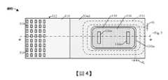
200、400:俯視圖200, 400: top view
300:圖像感測器300: Image sensor
302:光偵測器302: Light Detector
304a:第一介電層304a: first dielectric layer
304b:第二介電層304b: second dielectric layer
304c:第三介電層304c: third dielectric layer
304d:第四介電層304d: fourth dielectric layer
306:蝕刻停止層306: Etch Stop Layer
308:第一柵格層308: The first grid layer
310:第二柵格層310: The second grid layer
312:柵格結構312: grid structure
314:濾色器314: color filter
502:大致上筆直的線502: Roughly straight line
702:裝置STI結構702: Device STI structure
802:第一絕緣層802: first insulating layer
804:第二絕緣層804: second insulating layer
900、1000、1100、1200、1300、1400、1500、1600、1700、1800、1900、2000、2100、2300、2400、2500、2600、2700、2800、2900、3000、3200、3300、3400、3500、3600、3700、3800:剖面圖900, 1000, 1100, 1200, 1300, 1400, 1500, 1600, 1700, 1800, 1900, 2000, 2100, 2300, 2400, 2500, 2600, 2700, 2800, 2900, 3000, 3200, 3300, 3400, 3500, 3600, 3700, 3800: section view
902:掩蔽層902: masking layer
1002:深溝槽隔離層1002: deep trench isolation layer
1202:介電保護層1202: Dielectric protective layer
1302:柱塞開口1302: Plunger opening
1702:柱塞結構1702: Plunger structure
1802、2402:接合墊開口1802, 2402: Bonding pad opening
2002:接合墊層2002: Bonding cushion
2200:第一方法2200: The first method
2202、2204、2206、2208、2210、2212、2214、2216、2218、3102、3104、3106、3108、3110、3112、3114、3116、3118、3120、3902、3904、3906、3908、3910:動作2202, 2204, 2206, 2208, 2210, 2212, 2214, 2216, 2218, 31023104, 3106, 3108, 3110, 3112, 3114, 3116, 3118, 3120, 3902, 3904, 3906, 3908, 3910: Action
3100:第二方法3100: The second method
3402:接合墊隔離開口3402: Bonding pad isolation opening
3502:第一DTI層3502: The first DTI layer
3504:第二DTI層3504: The second DTI layer
3900:第三方法3900: third method
d1、d2、dv:距離d1 , d2 , dv : distance
Fig.1:圖1Fig.1: Picture 1
Fig.2:圖2Fig. 2: Fig. 2
Fig.3:圖3Fig. 3: Figure 3
Fig.4:圖4Fig. 4: Fig. 4
h1、h2、hbp、hd1:高度h1 , h2 , hbp , hd1 : height
Ti、Ts:厚度Ti , Ts : thickness
W1:寬度W1 : width
結合附圖閱讀以下詳細說明,會最佳地理解本發明的各個態樣。應注意,根據行業中的標準慣例,各種特徵並非按比例繪製。事實上,為論述清晰起見,可任意增大或減小各種特徵的尺寸。Each aspect of the present invention will be best understood by reading the following detailed description in conjunction with the accompanying drawings. It should be noted that, according to standard practices in the industry, various features are not drawn to scale. In fact, for clarity of discussion, the size of various features can be increased or decreased arbitrarily.
圖1示出包含延伸穿過半導體基板的接合墊的積體晶片的一些實施例的剖面圖。Figure 1 shows a cross-sectional view of some embodiments of an integrated wafer including bond pads extending through a semiconductor substrate.
圖2示出如由圖1及圖2中的切割線指示的圖1的IC的一些替代實施例的俯視圖。FIG. 2 shows a top view of some alternative embodiments of the IC of FIG. 1 as indicated by the cut lines in FIG. 1 and FIG. 2.
圖3示出包含與多個光偵測器橫向偏移的接合墊的圖像感測器的一些實施例的剖面圖。Figure 3 shows a cross-sectional view of some embodiments of an image sensor including bond pads laterally offset from a plurality of light detectors.
圖4示出如由圖3及圖4中的切割線指示的圖3的圖像感測器的一些替代實施例的俯視圖。Fig. 4 shows a top view of some alternative embodiments of the image sensor of Fig. 3 as indicated by the cut lines in Figs. 3 and 4.
圖5、圖6A、圖6B、圖7以及圖8示出包圍接合墊的接合墊隔離結構的一些替代實施例的剖面圖。5, 6A, 6B, 7 and 8 show cross-sectional views of some alternative embodiments of the bonding pad isolation structure surrounding the bonding pad.
圖9到圖21示出用於形成包圍接合墊的接合墊隔離結構的第一方法的一些實施例的一系列剖面圖。Figures 9-21 show a series of cross-sectional views of some embodiments of a first method for forming a bond pad isolation structure surrounding a bond pad.
圖22示出圖9到圖21的第一方法的一些實施例的方塊圖。Fig. 22 shows a block diagram of some embodiments of the first method of Figs. 9-21.
圖23到圖30示出用於形成包圍接合墊的接合墊隔離結構的第二方法的一些實施例的一系列剖面圖。Figures 23-30 show a series of cross-sectional views of some embodiments of a second method for forming a bond pad isolation structure surrounding a bond pad.
圖31示出圖23到圖30的第二方法的一些實施例的方塊圖。FIG. 31 shows a block diagram of some embodiments of the second method of FIGS. 23-30.
圖32到圖38示出用於形成包圍接合墊的接合墊隔離結構的第三方法的一些實施例的一系列剖面圖。Figures 32 to 38 show a method for forming a bonding pad isolation structure surrounding the bonding padA series of cross-sectional views of some embodiments of the third method.
圖39示出圖32到圖38的第三方法的一些實施例的方塊圖。FIG. 39 shows a block diagram of some embodiments of the third method of FIGS. 32 to 38.
以下揭露內容提供用於實作本發明的不同特徵的諸多不同的實施例或實例。以下闡述組件及排列的具體實例以簡化本揭露內容。當然,該些僅為實例且不旨在進行限制。舉例而言,以下說明中將第一特徵形成於第二特徵「之上」或第二特徵「上」可包括其中第一特徵及第二特徵被形成為直接接觸的實施例,且亦可包括其中第一特徵與第二特徵之間可形成有附加特徵、進而使得所述第一特徵與所述第二特徵可能不直接接觸的實施例。另外,本發明可能在各種實例中重複使用參考編號及/或字母。此種重複使用是出於簡潔及清晰的目的,但自身並不表示所論述的各種實施例及/或配置之間的關係。The following disclosure provides many different embodiments or examples for implementing different features of the present invention. Specific examples of components and arrangements are described below to simplify the disclosure. Of course, these are only examples and are not intended to be limiting. For example, in the following description, forming the first feature "on" or the second feature "on" may include an embodiment in which the first feature and the second feature are formed in direct contact, and may also include An embodiment in which additional features may be formed between the first feature and the second feature, so that the first feature and the second feature may not directly contact each other. In addition, the present invention may reuse reference numbers and/or letters in various examples. Such repeated use is for the purpose of brevity and clarity, but does not itself represent the relationship between the various embodiments and/or configurations discussed.
另外,為了易於描述圖中所示的一個元件或特徵與另一元件或特徵的關係,本文中可使用例如「在...下」、「在...下方」、「下部」、「上覆」、及「上部」等空間相對用語。除了圖中所繪示的取向之外,所述空間相對用語亦旨在涵蓋裝置在使用或操作時的不同取向。設備可被另外取向(旋轉90度或在其他取向),而本文所用的空間相對描述語可同樣相應地作出解釋。In addition, in order to easily describe the relationship between one element or feature shown in the figure and another element or feature, for example, "under", "below", "lower", "on" can be used herein. Relative terms such as "overlay" and "upper". In addition to the orientations depicted in the figure, the relative terms of space are also intended to cover different orientations of the device in use or operation. The device can be oriented in other ways (rotated by 90 degrees or in other orientations), and the spatial relative descriptors used herein can also be interpreted accordingly.
積體晶片通常包括沿著基板的前側佈置的多個金屬內連線層。多個金屬內連線層配置成將佈置在基板內的裝置(例如電晶體、光偵測器等)電性連接在一起。背側照射式CMOS圖像感測器(Back-side illuminated CMOS image sensor,BSI-CIS)包括光偵測器(photodetector),所述光偵測器接近於基板的背側而佈置於基板內,使光偵測器能夠沿著基板的背側接收光。藉由沿著基板的背側接收光,入射光不穿過多個金屬內連線層,藉此增加光偵測器的光學效率。Integrated wafers generally include multiple metal interconnect layers arranged along the front side of the substrate. The multiple metal interconnection layers are configured to connect devices (e.g., electricalCrystal, light detector, etc.) are electrically connected together. The back-side illuminated CMOS image sensor (BSI-CIS) includes a photodetector, which is arranged in the substrate close to the backside of the substrate, The light detector can receive light along the back side of the substrate. By receiving light along the back side of the substrate, the incident light does not pass through multiple metal interconnection layers, thereby increasing the optical efficiency of the photodetector.
借助於沿著基板的背側接收光的BSI-CIS,具有BSI-CIS的基板通常置於呈暴露出基板的背側的前側向下配置形式的封裝結構內。因為暴露出基板的背側,所以接合墊通常沿著基板的背側佈置且連接到金屬內連線層。接合墊可具有若干不同配置。舉例來說,接合墊可設置在接合墊開口內,所述接合墊開口延伸穿過基板的前側到基板的背側。為了將接合墊與基板電性隔離,介電結構沿著基板的界定接合墊開口的側壁設置。然而,沿著接合墊開口設置介電結構增加了與製造BSI-CIS相關聯的複雜度、時間以及成本。另外,接合墊的頂表面可設置在基板的背側下方。這可增加由光偵測器接收的光,然而,這將降低接合墊與另一接合結構之間的接合的可靠性。此外,接合墊可包括在基板的背側上方延伸的上部導電區段,藉此增加接合墊與另一接合結構之間的接合的可靠性。然而,在此類實施例中,上部導電區段可將光從光偵測器反射開,藉此降低從光偵測器再現(reproduce)的圖像的可靠性及/或品質。By means of the BSI-CIS that receives light along the back side of the substrate, the substrate with the BSI-CIS is usually placed in a package structure in the form of a front side downwardly exposing the back side of the substrate. Because the backside of the substrate is exposed, the bonding pads are usually arranged along the backside of the substrate and connected to the metal interconnection layer. The bonding pad can have several different configurations. For example, the bonding pad may be disposed in the bonding pad opening, which extends through the front side of the substrate to the back side of the substrate. In order to electrically isolate the bonding pad from the substrate, the dielectric structure is disposed along the sidewall of the substrate that defines the bonding pad opening. However, arranging the dielectric structure along the bonding pad opening increases the complexity, time, and cost associated with manufacturing BSI-CIS. In addition, the top surface of the bonding pad may be disposed under the back side of the substrate. This can increase the light received by the photodetector, however, it will reduce the reliability of the bonding between the bonding pad and another bonding structure. In addition, the bonding pad may include an upper conductive section extending above the back side of the substrate, thereby increasing the reliability of the bonding between the bonding pad and another bonding structure. However, in such embodiments, the upper conductive section can reflect light away from the photodetector, thereby reducing the reliability and/or quality of the image reproduced from the photodetector.
因此,在一些實施例中,本公開涉及一種包含包圍接合墊的接合墊隔離結構的積體晶片。積體晶片包含佈置在基板內的多個光偵測器。接合墊區在與光偵測器橫向偏移的位置處延伸穿過基板到金屬內連線(metal interconnect wire),所述金屬內連線佈置在沿著基板的前側設置的內連線介電結構內。接合墊設置在接合墊區內且從基板的前側延伸到基板的背側並電性耦接到金屬內連線。在一些實施例中,接合墊直接接觸基板的上表面且接觸基板的側壁。接合墊隔離結構具有環形形狀且橫向包圍接合墊。另外,接合墊隔離結構從基板的背側延伸到前側,藉此將接合墊與設置在基板上及/或基板內的裝置(例如光偵測器及/或電晶體)電性隔離。接合墊與基板接觸減少了與形成接合墊相關聯的複雜度、時間以及成本。另外,接合墊隔離結構防止從接合墊到設置在基板上及/或基板內的裝置的“洩漏”(即電流流動)。Therefore, in some embodiments, the present disclosure relates to aThe bonding pad of the pad isolates the integrated wafer of the structure. The integrated wafer includes a plurality of light detectors arranged in a substrate. The bonding pad area extends across the substrate to a metal interconnect wire at a position laterally offset from the photodetector, and the metal interconnect wire is arranged on an interconnect dielectric disposed along the front side of the substrate. Within the structure. The bonding pad is arranged in the bonding pad area and extends from the front side of the substrate to the back side of the substrate and is electrically coupled to the metal interconnection. In some embodiments, the bonding pad directly contacts the upper surface of the substrate and contacts the sidewall of the substrate. The bonding pad isolation structure has a ring shape and laterally surrounds the bonding pad. In addition, the bonding pad isolation structure extends from the backside to the front side of the substrate, thereby electrically isolating the bonding pads from devices (such as photodetectors and/or transistors) disposed on and/or in the substrate. Contacting the bonding pads with the substrate reduces the complexity, time, and cost associated with forming bonding pads. In addition, the bonding pad isolation structure prevents "leakage" (ie, current flow) from the bonding pad to the device provided on and/or within the substrate.
圖1示出具有設置在接合墊區101b內的接合墊116的積體晶片100的一些實施例的剖面圖。FIG. 1 shows a cross-sectional view of some embodiments of an
積體晶片100包含沿著半導體基板110(例如矽基板)的前側110fs設置的內連線結構104。內連線結構104上覆於載體基板102(例如矽基板),其中內連線結構104設置在半導體基板110與載體基板102之間。內連線結構104包含佈置在內連線介電結構103內的多個內連線層。多個內連線層在導電線108與導通孔106之間交替。導電線108配置成提供橫向連接(即平行於載體基板102的上表面的連接),而導通孔106配置成提供相鄰導電線108之間的豎直連接。導電線108包含上部導電線層108a。介電結構118上覆於半導體基板110的背側110bs。淺溝槽隔離(shallow trench isolation,STI)結構112設置在半導體基板110內並且沿著內連線介電結構103的上表面延伸。The
接合墊區101b在與裝置區101a橫向偏移的位置處延伸穿過半導體基板110到上部導電線層108a。在一些實施例中,裝置區101a包含設置在半導體基板110內及/或半導體基板110上的一個或多個半導體裝置120(例如電晶體、電阻器、變容器等)及/或光偵測器(未示出)。接合墊116和接合墊隔離結構114設置在接合墊區101b內。接合墊116包含上部導電主體116a和位於上部導電主體116a之下的導電突部116b。上部導電主體116a包括與導電突部116b相同的材料(例如鋁、銅)。在一些實施例中,上部導電主體116a直接上覆於半導體基板110的上表面110us且直接接觸所述上表面110us。在此類實施例中,導電突部116b直接接觸半導體基板110的側壁,並且從上部導電主體116a延伸到上部導電線層108a。另外,上部導電主體116a具有界定上覆於導電突部116b的接墊開口116o的側壁。接合墊116可配置成將一個或多個半導體裝置120電性耦接到另一積體晶片(未示出)。在一些實施例中,上部導電主體116a與半導體基板110的內部側壁110is橫向偏移非零距離(non-zero distance)。The
接合墊隔離結構114與接合墊116的外部側壁橫向偏移且包圍所述外部側壁。在一些實施例中,接合墊隔離結構114包括與半導體基板110不同的材料(例如二氧化矽)。接合墊隔離結構114可從半導體基板110的前側110fs延伸到背側110bs。在一些實施例中,接合墊隔離結構114具有高度h1,所述高度h1大於或等於半導體基板110的高度h2。接合墊隔離結構114配置成將接合墊116與設置在半導體基板110內及/或半導體基板110上的其它裝置(例如半導體裝置120)及/或摻雜區(未示出)電性隔離。這可減少及/或防止接合墊116與設置在半導體基板110內及/或半導體基板110上的其它裝置及/或摻雜區之間的“洩漏”(即電流流動),藉此增加積體晶片100的可靠性和承受能力。另外,在一些實施例中,當接合墊116直接接觸半導體基板110時,可減少與形成積體晶片100相關聯的複雜度、成本以及時間。The outer sidewalls of the bonding
圖2示出如由圖1和圖2中的切割線指示的圖1的積體晶片100的一些替代實施例的俯視圖200。為了便於說明,已從圖2的俯視圖200省略圖1的介電結構118。FIG. 2 shows a
如圖2中所示出,接合墊隔離結構114具有環狀形狀,其中接合墊隔離結構114的內部側壁完全包圍接合墊116的外部側壁。接合墊隔離結構114的內部側壁與接合墊隔離結構114的外部側壁橫向偏移距離d1。在一些實施例中,距離d1是非零的。當從上方觀察時,接合墊隔離結構114具有帶圓化邊緣的矩形/正方形形狀,然而,接合墊隔離結構114可具有其它形狀,例如圓形/橢圓形狀。當從上方觀察時,接合墊116具有帶圓化邊緣的矩形/正方形形狀,然而,接合墊116可具有其它形狀,例如圓形/橢圓形狀。在一些實施例中,接合墊隔離結構114的形狀對應於接合墊116的形狀。另外,接合墊116的界定接墊開口116o的側壁彼此橫向偏移非零距離。在一些實施例中,焊料凸塊(未示出)可橫向設置在接墊開口116o之間。當從上方觀察時,接墊開口116o可例如具有正方形/矩形形狀。接合墊隔離結構114連續環繞接合墊116的外部側壁且從半導體基板110的前側(圖1的前側110fs)延伸到背側(圖1的背側110bs)。因此,接合墊隔離結構114將接合墊116與設置在半導體基板110內及/或半導體基板110上的其它半導體裝置及/或摻雜區電性隔離。STI結構112直接位於接合墊116之下。在一些實施例中,接合墊116的外部側壁在STI結構112的外部側壁之間橫向隔開。As shown in FIG. 2, the bonding
圖3示出包含與多個光偵測器302橫向偏移的接合墊116的圖像感測器300的一些實施例的剖面圖。FIG. 3 shows a cross-sectional view of some embodiments of an
半導體基板110上覆於載體基板102。在一些實施例中,半導體基板110及/或載體基板102可例如分別為塊狀基板(例如塊狀矽基板)、絕緣體上矽(silicon-on-insulator,SOI)基板或一些其它合適的基板。多個光偵測器302設置在半導體基板110內。在一些實施例中,光偵測器302分別從半導體基板110的背側110bs延伸到背側110bs下方的點。在另外的實施例中,所述點位於半導體基板110的前側110fs處,所述前側110fs與半導體基板110的背側110bs相對。內連線結構104沿著半導體基板110的前側110fs設置。內連線結構104包含內連線介電結構103、多個導電線108以及多個導通孔106。半導體基板110藉由內連線結構104接合到載體基板102。在一些實施例中,導電線108及/或導通孔106可例如分別為或包括鋁、銅、鋁銅、鎢等。在一些實施例中,內連線介電結構103可例如包括一個或多個介電層(例如二氧化矽)。The
介電結構118上覆於半導體基板110的背側110bs。在一些實施例中,介電結構118包含一個或多個介電層,例如第一介電層304a、第二介電層304b、第三介電層304c以及第四介電層304d。在一些實施例中,第一介電層304a可例如為或包括金屬氧化物,例如氧化鋁(aluminum oxide)或另一合適的氧化物。第二介電層304b可例如為或包括金屬氧化物,例如氧化鉿(hafnium oxide)或另一合適的氧化物。第三介電層304c可例如為或包括金屬氧化物,例如氧化鉭(tantalum oxide)或另一合適的氧化物。第四介電層304d可例如為或包括氧化物(例如二氧化矽、另一合適的氧化物)、未摻雜矽玻璃(undoped silicon glass,USG)、多晶矽、另一合適的介電質及/或可具有在約500埃到3,000埃的範圍內的厚度。介電結構118可配置成保護半導體基板110的背側110bs。The
蝕刻停止層306上覆於介電結構118。第一柵格層308上覆於蝕刻停止層306,並且第二柵格層310上覆於第一柵格層308。柵格(grid)結構312包含豎直地位於光偵測器302上方的第一柵格層308和第二柵格層310的區段。柵格結構312橫向地位於光偵測器302周圍和之間以界定多個濾色器開口。多個濾色器(color filter)314佈置在多個濾色器開口內且上覆於多個光偵測器302。柵格結構312包括折射率小於濾色器314的折射率的介電材料。由於較低折射率,柵格結構312充當用於將入射電磁輻射(即光)導引到對應光偵測器302的輻射導件(radiation guide)。另外,濾色器314分別配置成阻斷入射電磁輻射的第一頻率範圍,同時將入射電磁輻射的第二頻率範圍(與第一頻率範圍不同)傳遞到下伏的光偵測器302。The
在一些實施例中,蝕刻停止層306可例如為或包括碳化矽、氮化矽等及/或可具有約1,500埃的厚度。在一些實施例中,第一柵格層308可例如為或包括氧化物(例如二氧化矽或另一合適的氧化物)及/或可具有約5,600埃的厚度。在另外的實施例中,第二柵格層310可例如為或包括氧化物(例如氮氧化矽或另一合適的氧化物)及/或可具有約1,500埃的厚度。在再一些實施例中,第一柵格層308可為或包括金屬,例如鎢、另一合適的金屬等。在此類實施例中,柵格結構312可配置為包括一個或多個金屬層和一個或多個介電層的組合柵格結構。在另外的實施例中,柵格結構312可配置為包括一個或多個介電層的介電柵格結構。In some embodiments, the
一個或多個半導體裝置120(例如電晶體、電阻器等)可設置在半導體基板的前側110fs內及/或半導體基板的前側110fs上。在此類實施例中,一個或多個半導體裝置120可例如為像素裝置,例如轉移電晶體(transfer transistor)、源極跟隨器電晶體(source follower transistor)、復位電晶體(reset transistor)等。一個或多個半導體裝置120、光偵測器302以及柵格結構312橫向佈置在圖像感測器300的裝置區101a內。裝置區101a與圖像感測器300的接合墊區101b橫向偏移。接合墊116和接合墊隔離結構114橫向佈置在圖像感測器300的接合墊區101b內。因此,在一些實施例中,接合墊116和接合墊隔離結構114與光偵測器302及/或一個或多個半導體裝置120橫向偏移非零距離。One or more semiconductor devices 120 (for example, transistors, resistors, etc.) may be disposed in the front side 110fs of the semiconductor substrate and/or on the front side 110fs of the semiconductor substrate. In such an embodiment, the one or
接合墊116配置成藉由內連線結構104將一個或多個半導體裝置120及/或光偵測器302電性耦接到另一積體晶片(未示出)。在一些實施例中,接合墊116直接接觸半導體基板110的上表面110us,並且具有延伸穿過半導體基板110到上部導電線層108a的突部。在此類實施例中,突部直接接觸設置在半導體基板110的上表面110us下方的半導體基板110的側壁。突部延伸穿過淺溝槽隔離(shallow trench isolation,STI)結構112和內連線介電結構103。另外,接合墊116具有界定上覆於接合墊116的突部的接墊開口116o的側壁。在另外的實施例中,接合墊116與半導體基板110的上部側壁和介電結構118的側壁橫向偏移距離d2。在一些實施例中,距離d2是非零的,使接合墊116可與介電結構118電性隔離。另外,在此類實施例中,藉由非零距離d2,可保護半導體基板110的上部側壁及/或介電結構118的側壁以免受到對接合墊116執行的接合製程的影響(即以免受到施加到接合墊116的向下的力的影響)。這可增加圖像感測器300的結構完整性。在一些實施例中,接合墊116的頂表面與介電結構118的頂表面(未示出)對準(例如參看圖5)。接合墊116具有界定為從半導體基板110的上表面110us到接合墊116的頂表面的接合墊高度hbp。在一些實施例中,接合墊高度hbp為約12,000埃。The
接合墊隔離結構114橫向包圍接合墊116,其中接合墊隔離結構114從半導體的背側110bs延伸到前側110fs下方的點。因此,接合墊隔離結構114將接合墊116與一個或多個半導體裝置120及/或光偵測器302電性隔離,藉此防止接合墊116與相鄰裝置之間的“洩漏”(即電流流動)。這提高了圖像感測器300的性能、穩定性以及可靠性。接合墊隔離結構114具有高度h1,所述高度h1大於半導體基板110的高度h2。接合墊隔離結構114的底表面豎直地位於半導體基板110的前側110fs下方,間隔距離dv。在一些實施例中,距離dv是非零的,其中接合墊隔離結構114延伸到內連線介電結構103中。在一些實施例中,如果接合墊隔離結構114的底表面位於前側110fs上方(即距離dv為負及/或高度h1小於高度h2),那麼“洩漏”可出現在接合墊116與一個或多個半導體裝置120及/或光偵測器302之間,藉此降低圖像感測器300的性能。接合墊隔離結構114可例如為或包括氧化物,例如二氧化矽或氮化矽、氮氧化矽等。The bond
圖4示出如由圖3和圖4中的切割線指示的圖3的圖像感測器300的一些替代實施例的俯視圖400。FIG. 4 shows a
如圖4中所示出,接合墊隔離結構114具有環狀形狀,其中接合墊隔離結構114的內部側壁完全包圍接合墊116的外部側壁。接合墊116的外部側壁與半導體基板110的內部側壁110is橫向偏移距離d2。在一些實施例中,距離d2是非零的。濾色器314佈置成包括行和列的陣列且分別上覆於光偵測器(圖3的光偵測器302)。在一些實施例中,當從上方觀察時,濾色器314分別具有矩形/正方形形狀及/或圓形/橢圓形狀(未示出)。As shown in FIG. 4, the bonding
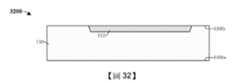
圖5示出具有由接合墊隔離結構114包圍的接合墊116的積體晶片500的一些替代實施例的剖面圖。FIG. 5 shows a cross-sectional view of some alternative embodiments of an
接合墊116的頂表面116ts和介電結構118的頂表面分別沿著大致上筆直的線502對準。在一些實施例中,大致上筆直的線502平行於半導體基板110的背側110bs。在另外的實施例中,接合墊116的頂表面116ts位於介電結構118的頂表面上方(未示出)。另外,接合墊隔離結構114具有傾斜側壁,其中接合墊隔離結構114的寬度W1從半導體基板110的背側110bs到半導體基板110的前側110fs連續增大。在此類實施例中,在形成積體晶片500期間,接合墊隔離結構114可例如已經與STI結構112同時形成或在形成STI結構112之後且在形成內連線結構104之前形成。在一些實施例中,例如大致上筆直的線502配置為平坦的水平線。在另外的實施例中,大致上筆直的線502可在與沿著接合墊116的頂表面116ts設置的平坦的水平線相距-25埃到25埃的範圍內變化或在與所述平坦的水平線相距-5埃到5埃的範圍內變化。在再一些實施例中,在沿著大致上筆直的線502設置的第一點與沿著大致上筆直的線502設置的第二點之間界定出一個角度,其中所述第一點與所述第二點橫向偏移並且所述角度為約180度。The top surface 116ts of the
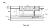
圖6A示出具有由接合墊隔離結構114包圍的接合墊116的積體晶片600的一些替代實施例的剖面圖。FIG. 6A shows a cross-sectional view of some alternative embodiments of an
接合墊隔離結構114從半導體基板110的背側110bs延伸到半導體基板110的前側110fs下方的點。在一些實施例中,接合墊隔離結構114的底表面可與半導體基板110的前側110fs對準(未示出)。接合墊隔離結構114具有傾斜側壁,其中接合墊隔離結構114的寬度W1從半導體基板110的背側110bs到半導體基板110的前側110fs連續減小。在此類實施例中,在形成積體晶片600期間,接合墊隔離結構114可例如已在形成內連線結構104之後形成。The bond
圖6B示出圖6A的積體晶片600的一些替代實施例的剖面圖,其中接合墊隔離結構114在STI結構112的外部側壁之間橫向隔開。FIG. 6B shows a cross-sectional view of some alternative embodiments of the
圖7示出具有與接合墊區101b橫向偏移的裝置區101a的積體晶片700的一些替代實施例的剖面圖。Figure 7 shows a cross-sectional view of some alternative embodiments of an
裝置STI結構702設置在裝置區101a內,其中裝置STI結構702包括與STI結構112相同的材料。在一些實施例中,裝置STI結構702具有分別與STI結構112的底表面和頂表面對準的底表面和頂表面。在另外的實施例中,裝置STI結構702具有環形形狀且包圍設置在半導體基板110內及/或半導體基板110上的至少一個半導體裝置120。裝置STI結構702可進一步增加半導體裝置120與接合墊116之間的電性隔離。另外,接合墊隔離結構114的底表面與STI結構112的底表面及/或裝置STI結構702的底表面對準。在一些實施例中,STI結構112在接合墊隔離結構114的外部側壁之間連續延伸,其中STI結構112進一步增加接合墊116與設置在半導體基板110上及/或半導體基板110內的其它裝置(例如半導體裝置120、光偵測器(未示出)等)之間的電性隔離。在另外的實施例中,STI結構112和接合墊隔離結構114包括相同材料,其中接合墊隔離結構114是STI結構112的突部。The
圖8示出具有圍繞接合墊116設置的接合墊隔離結構114的積體晶片800的一些替代實施例的剖面圖。FIG. 8 shows a cross-sectional view of some alternative embodiments of an
第一絕緣層802沿著介電結構118的側壁和半導體基板110的側壁設置。第一絕緣層802設置在接合墊116與半導體基板110的上表面110us之間。接合墊116包含設置在半導體基板110的上表面110us上方的導電主體和從所述導電主體延伸到上部導電線層108a的導電突部。第二絕緣層804沿著第一絕緣層802的側壁且沿著接合墊116的突部的側壁設置。第二絕緣層804設置在半導體基板110的側壁與接合墊116的突部之間,其中第二絕緣層804圍繞相應的突部連續延伸。第一絕緣層802和第二絕緣層804分別配置成將接合墊116與半導體基板110電性隔離。這進一步提高了積體晶片800的性能和可靠性。在一些實施例中,第一絕緣層802可例如為或包括氧化物,例如二氧化矽、未摻雜矽玻璃二氧化矽(undoped silicon glass silicon dioxide,USGOX)、另一合適的氧化物等。在一些實施例中,第二絕緣層804可例如為或包括氧化物,例如二氧化矽、USGOX、另一合適的氧化物等。The first insulating
圖9到圖21示出根據本公開的各個方面的形成包含接合墊隔離結構的積體晶片的第一方法的一些實施例的剖面圖900到剖面圖2100,所述接合墊隔離結構包圍接合墊。雖參照第一方法描述圖9到圖21中所示的剖面圖900到剖面圖2100,但應瞭解,圖9到圖21中所示的結構不限於所述方法而實際上可單獨獨立於所述方法。雖然將圖9到圖21描述為一系列動作,但應瞭解,這些動作不限於所述動作的次序可在其它實施例中更改,並且所公開的方法還適用於其它結構。在其它實施例中,示出及/或描述的一些動作可完全或部分地省略。9 to 21 show
如圖9的剖面圖900所示,提供半導體基板110且在所述半導體基板110的前側110fs上形成掩蔽層902。在一些實施例中,半導體基板110可例如為塊狀基板(例如塊狀矽基板)、絕緣體上矽(SOI)基板或一些其它合適的基板。在半導體基板110的前側110fs上形成淺溝槽隔離(STI)結構112。在一些實施例中,用於形成STI結構112的製程可包含:選擇性地蝕刻半導體基板110以形成延伸到半導體基板110的前側110fs中的溝槽;以及(例如藉由化學氣相沉積(chemical vapor deposition,CVD)、物理氣相沉積(physical vapor deposition,PVD)、原子層沉積(atomic layer deposition,ALD)、熱氧化(thermal oxidation)等)用介電材料(例如二氧化矽、碳化矽等)填充溝槽。在另外的實施例中,藉由使半導體基板110的未掩蔽部分暴露於配置成選擇性地去除半導體基板110的未掩蔽部分的一種或多種蝕刻劑來選擇性地蝕刻半導體基板110。掩蔽層902可例如為或包括氮氧化矽(silicon-oxy-nitride)。As shown in the
如圖10的剖面圖1000所示,在半導體基板110上方及其中形成深溝槽隔離(deep trench isolation,DTI)層1002。在一些實施例中,用於形成DTI層1002的製程包含:在掩蔽層902和STI結構112上方形成第二掩蔽層;根據所述第二掩蔽層來使半導體基板110和掩蔽層902圖案化,藉此在半導體基板110中形成DTI開口;(例如藉由電漿增強CVD(plasma-enhanced CVD,PECVD)製程、高深寬比製程(high aspect ratio process,HARP)、PVD或另一合適的沉積製程)在半導體基板110上方形成DTI材料(例如氧化矽、氮化矽、氮氧化矽、電漿增強氧化物(plasma-enhanced oxide,PEOX)、另一合適的介電材料等),其中DTI材料填充DTI開口。在一些實施例中,形成DTI材料包含:在第二介電層(例如包括氮化矽)上方形成第一介電層(例如包括氧化矽),第二介電層對DTI開口進行加襯(line),並且第一介電層填充DTI開口的其餘部分。在一些實施例中,DTI層1002的底表面設置在半導體基板110的背側110bs上方。在一些實施例中,藉由例如CVD、PVD、ALD或另一合適的沉積製程來形成DTI層1002。在一些實施例中,DTI層1002具有在約12,000埃到15,000埃的範圍內或大於20,000埃的高度hd1。As shown in the
如圖11的剖面圖1100所示,對DTI層(圖10的DTI層1002)執行平坦化製程,藉此界定接合墊隔離結構114。在一些實施例中,平坦化製程包含:對DTI層(圖10的DTI層1002)及/或STI結構112執行化學機械平坦化(chemical-mechanical planarization,CMP),直到到達半導體基板110的前側110fs為止。在另外的實施例中,平坦化製程可去除掩蔽層902。在一些實施例中,在執行平坦化製程之後,接合墊隔離結構114具有大於2微米的高度h1。在另外的實施例中,接合墊隔離結構114的寬度W1從前側110fs到半導體基板110的背側110bs上方的點連續減小。As shown in the
在一些實施例中,平坦化製程包含:對DTI層(圖10的DTI層1002)執行CMP,直到暴露出STI結構112的頂表面為止,藉此界定接合墊隔離結構114(未示出)。在此類實施例中,如圖7的剖面圖所示出,STI結構112的上表面和接合墊隔離結構114的上表面分別與半導體基板110的前側110fs豎直地偏移。另外,在此類實施例中,在執行平坦化之後,執行去除製程以去除掩蔽層902(未示出)。In some embodiments, the planarization process includes: performing CMP on the DTI layer (
如圖12的剖面圖1200所示,在半導體基板110的前側110fs上形成內連線結構104。內連線結構104包含內連線介電結構103、多個導電線108以及多個導通孔106。在一些實施例中,內連線介電結構103可為或包括一個或多個層間介電(inter-level dielectric,ILD)層。一個或多個ILD層可例如為或包括氧化物,如二氧化矽或另一合適的氧化物。在一些實施例中,用於形成內連線結構104的製程包含:藉由單鑲嵌製程或雙鑲嵌製程來形成導通孔106和導電線108。舉例來說,導通孔106的第一層和導電線108的第一層可分別藉由單鑲嵌製程來形成。另外,在此類實施例中,製程包含:藉由反覆執行雙鑲嵌製程來形成導電線108和導通孔106的其餘層。在一些實施例中,導電線108及/或導通孔106可例如分別為或包括鋁、銅、鋁銅、鎢等。As shown in the
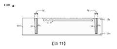
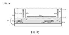
如圖13的剖面圖1300所示,圖12的結構經旋轉180度,並且內連線結構104接合到載體基板102。在一些實施例中,接合製程可包括熔融接合(fusion bonding)製程。在一些實施例中,載體基板102可例如為塊狀基板(例如塊狀矽基板)、絕緣體上矽(SOI)基板或一些其它合適的基板。在一些實施例中,在執行接合製程之後,對半導體基板110執行薄化製程,直到暴露出接合墊隔離結構114為止。在此類實施例中,薄化製程將半導體基板110的初始厚度Ti減小到厚度Ts。在一些實施例中,厚度Ts等於接合墊隔離結構114的高度h1。在另外的實施例中,藉由機械研磨製程、CMP、一些其它薄化製程或前述內容的任何組合來執行薄化製程。舉例來說,薄化製程可完全由機械研磨製程執行。As shown in the
如圖14的剖面圖1400所示,在半導體基板110的背側110bs上方形成介電結構118。在一些實施例中,介電結構118包含一個或多個介電層,例如第一介電層304a、第二介電層304b、第三介電層304c以及第四介電層304d。在一些實施例中,第一介電層304a、第二介電層304b、第三介電層304c及/或第四介電層304d可分別藉由CVD、PVD、ALD或另一合適的沉積製程來形成。在另外的實施例中,第一介電層、第二介電層、第三介電層和第四介電層304a-d可分別包括彼此不同的介電材料。舉例來說,第一介電層304a可包括氧化鋁,第二介電層304b可包括氧化鉿,第三介電層304c可包括氧化鉭,並且第四介電層304d可包括二氧化矽。第四介電層304d可例如具有約1,300埃的厚度。另外,在介電結構118上方形成介電保護層1202。介電保護層1202可包括氧化物(例如二氧化矽)及/或可在後續處理步驟期間充當介電結構118的硬質遮罩(hard mask)保護層。在一些實施例中,介電保護層1202可例如具有約4,500埃的厚度。在此類實施例中,介電保護層1202的厚度足夠大(例如約4,500埃),使得第四介電層的厚度未在後續處理步驟(例如圖15的第一蝕刻製程及/或圖16的第二蝕刻製程)期間減小。在一些實施例中,介電結構118具有約2,000埃的厚度t1。As shown in the
如圖15的剖面圖1500所示,對介電保護層1202、介電結構118以及半導體基板110執行第一蝕刻製程,藉此形成柱塞開口(plug opening)1302。在一些實施例中,第一蝕刻製程可包含:執行濕式蝕刻製程、乾式蝕刻製程或另一合適的蝕刻製程。在一些實施例中,第一蝕刻製程包含:在介電保護層1202上方形成掩蔽層(未示出);使介電保護層1202的未掩蔽區和底層暴露於一種或多種蝕刻劑,藉此界定柱塞開口1302;以及執行去除製程以去除掩蔽層。As shown in the
如圖16的剖面圖1600所示,對STI結構112、內連線介電結構103以及介電保護層(介電保護層1202)執行第二蝕刻製程。這擴大柱塞開口1302且暴露出上部導電線層108a的上表面。在一些實施例中,第二蝕刻製程可包含:執行濕式蝕刻製程、乾式蝕刻製程或另一合適的蝕刻製程。在一些實施例中,第二蝕刻製程可包含:對圖15的結構執行毯覆式乾式蝕刻(blanket dry etch)製程。在此類實施例中,可藉由毯覆式乾式蝕刻製程來去除介電保護層(介電保護層1202)及/或在執行第二蝕刻製程之後,第四介電層304d的厚度可例如為約1,300埃。As shown in the
如圖17的剖面圖1700所示,在柱塞開口1302的至少一部分內形成柱塞結構1702。在一些實施例中,柱塞結構1702的上表面設置在半導體基板110的背側110bs下方。在一些實施例中,用於形成柱塞結構1702的製程包含:在柱塞開口1302內形成柱塞材料;以及執行回蝕(etch back)製程(例如乾式蝕刻製程、濕式蝕刻製程等)以去除柱塞材料的至少一部分,藉此界定柱塞結構1702。As shown in the
如圖18的剖面圖1800所示,對介電結構118和半導體基板110執行第三蝕刻製程,藉此界定接合墊開口1802。第三蝕刻製程界定半導體基板110的上表面110us,其中半導體基板110的上表面110us位於柱塞結構1702的上表面下方。在一些實施例中,第三蝕刻製程可包含:執行濕式蝕刻製程、乾式蝕刻製程或另一合適的蝕刻製程。在一些實施例中,第三蝕刻製程包含:在介電結構118上方形成掩蔽層(未示出);使介電結構118和半導體基板110的未掩蔽區暴露於一種或多種蝕刻劑,藉此界定接合墊開口1802;以及執行去除製程以去除掩蔽層。As shown in the
如圖19的剖面圖1900所示,執行柱塞去除製程以去除柱塞結構1702,藉此擴大接合墊開口1802且暴露出上部導電線層108a的上表面。在一些實施例中,柱塞去除製程包含:執行濕式灰化(wet ash)製程及/或乾式灰化(dry ash)製程,接著執行濕式蝕刻製程。As shown in the
如圖20的剖面圖2000所示,在圖19的結構上方形成接合墊層2002。在一些實施例中,可例如藉由無電式鍍覆、電鍍、濺射或另一合適的沉積製程來沉積及/或生長接合墊層2002。在另外的實施例中,接合墊層2002可例如為或包括鋁、銅、鋁銅等。在一些實施例中,接合墊層2002可包括與導通孔106及/或導電線108相同的材料。As shown in the
如圖21的剖面圖2100所示,對接合墊層(圖20的接合墊層2002)執行第四蝕刻製程,藉此界定接合墊116。接合墊116與半導體基板110和介電結構118的側壁橫向偏移距離d2。在一些實施例中,距離d2是非零的。在另外的實施例中,第四蝕刻製程包含:在接合墊層(圖20的接合墊層2002)上方形成掩蔽層(未示出);使接合墊層(圖20的接合墊層2002)的未掩蔽區暴露於一種或多種蝕刻劑,藉此界定接合墊116;以及執行去除製程以去除掩蔽層。As shown in the
雖然圖9到圖13描述在半導體基板110的前側110fs上形成內連線結構104之前形成接合墊隔離結構114,但應瞭解,形成接合墊隔離結構114不限於此類製造方法。舉例來說,在一些實施例中,可在形成內連線結構104之後形成接合墊隔離結構114,其中接合墊隔離結構114延伸到內連線介電結構103的上表面中(例如參照圖6A的積體晶片600)。在此類實施例中,接合墊隔離結構114可例如在圖13的薄化製程之後但在形成介電結構118之前形成。在再一些實施例中,接合墊隔離結構114可例如在形成接合墊116之後形成。在此類實施例中,接合墊隔離結構114延伸穿過介電結構118到半導體基板110的前側110fs(未示出)。Although FIGS. 9 to 13 describe the formation of the bonding
圖22示出根據本公開的形成積體電路的第一方法2200。雖然將第一方法2200示出及/或描述為一系列動作或事件,但應瞭解,所述方法不限於所示出的次序或動作。因此,在一些實施例中,動作可以與所示出的不同次序進行及/或可同時進行。另外,在一些實施例中,所示出的動作或事件可細分成多個動作或事件,其可與其它動作或子動作在不同時間進行或同時進行。在一些實施例中,可省略一些所示出的動作或事件,並且可包含其它未示出的動作或事件。FIG. 22 shows a
在動作2202處,在半導體基板的前側上形成淺溝槽隔離(STI)結構。圖9示出對應於動作2202的一些實施例的剖面圖900。At
在動作2204處,在半導體基板中形成接合墊隔離結構。接合墊隔離結構從半導體基板的前側延伸到半導體基板的背側。圖10和圖11示出對應於動作2204的一些實施例的剖面圖1000和剖面圖1100。At
在動作2206處,在半導體基板的前側上形成內連線結構。內連線結構包含上部導電線層。圖12示出對應於動作2206的一些實施例的剖面圖1200。At
在動作2208處,在半導體基板的背側上方形成介電結構。圖14示出對應於動作2208的一些實施例的剖面圖1400。At
在動作2210處,執行蝕刻製程以界定半導體基板中的柱塞開口,藉此暴露出上部導電線層的上表面。圖15和圖16示出對應於動作2210的一些實施例的剖面圖1500和剖面圖1600。At
在動作2212處,在柱塞開口中形成柱塞。柱塞的上表面設置在半導體基板的前側與背側之間。圖17示出對應於動作2212的一些實施例的剖面圖1700。At
在動作2214處,使介電結構和半導體基板圖案化,藉此界定接合墊開口和半導體基板的上表面。圖18示出對應於動作2214的一些實施例的剖面圖1800。At
在動作2216處,去除柱塞,藉此擴大接合墊開口且暴露出上部導電線層的上表面。圖19示出對應於動作2216的一些實施例的剖面圖1900。At
在動作2218處,在接合墊開口中形成接合墊。接合墊隔離結構圍繞接合墊連續延伸。圖20和圖21示出對應於動作2218的一些實施例的剖面圖2000和剖面圖2100。At
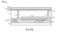
圖23到圖30示出根據本公開的各個方面的形成包含接合墊隔離結構的積體晶片的第二方法的一些實施例的剖面圖2300到剖面圖3000,所述接合墊隔離結構包圍接合墊。雖參照第二方法描述圖23到圖30中所示的剖面圖2300到剖面圖3000,但應瞭解,圖23到圖30中所示的結構不限於所述方法而實際上可單獨獨立於所述方法。雖然將圖23到圖30描述為一系列動作,但應瞭解,這些動作不限於所述動作的次序可在其它實施例中更改,並且所公開的方法還適用於其它結構。在其它實施例中,示出及/或描述的一些動作可完全或部分地省略。Figures 23 to 30 show
如圖23的剖面圖2300所示,在半導體基板110上方形成介電結構118。在一些實施例中,如圖9到圖14中所示出及/或描述形成圖23的結構。As shown in the
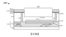
如圖24的剖面圖2400所示,對介電結構118和半導體基板110執行第一蝕刻製程,藉此形成接合墊開口2402。在一些實施例中,第一蝕刻製程可例如為或包括乾式蝕刻製程、濕式蝕刻製程或另一合適的蝕刻製程。在一些實施例中,第一蝕刻製程包含:在介電結構118上方形成掩蔽層(未示出);使介電結構118和半導體基板110的未掩蔽區暴露於一種或多種蝕刻劑,藉此界定接合墊開口2402;以及執行去除製程以去除掩蔽層。在一些實施例中,第一蝕刻製程界定設置在半導體基板110的背側110bs下方的半導體基板110的上表面110us。As shown in the
如圖25的剖面圖2500所示,在介電結構118和半導體基板110上方形成第一絕緣層802,其中第一絕緣層802對接合墊開口2402的至少一部分進行加襯。在一些實施例中,第一絕緣層802可例如為或包括氧化物(如氧化矽或另一合適的氧化物)及/或具有約4,500埃的厚度。在另外的實施例中,第一絕緣層802的厚度足夠大(例如約4,500埃),使第四介電層304d的厚度未在後續處理步驟(例如圖28的第三蝕刻製程)期間減小。As shown in the
如圖26的剖面圖2600所示,對第一絕緣層802和半導體基板110執行第二蝕刻製程,藉此擴大接合墊開口2402且暴露出STI結構112的上表面。在一些實施例中,第二蝕刻製程包含:在第一絕緣層802上方形成掩蔽層(未示出);使第一絕緣層802和半導體基板110的未掩蔽區暴露於一種或多種蝕刻劑,藉此暴露出STI結構112的上表面;以及執行去除製程以去除掩蔽層。As shown in the
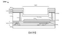
如圖27的剖面圖2700所示,在第一絕緣層802和半導體基板110上方形成第二絕緣層804。第二絕緣層804對接合墊開口2402進行加襯。在一些實施例中,第二絕緣層804可例如藉由PVD、CVD或另一合適的沉積製程來形成。在一些實施例中,第二絕緣層804可例如為或包括氧化物,如氧化矽或另一合適的氧化物。As shown in the
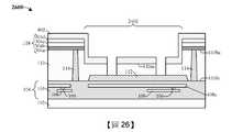
如圖28的剖面圖2800所示,對第一絕緣層802和第二絕緣層804、STI結構112以及內連線介電結構103執行第三蝕刻製程,藉此暴露出上部導電線層108a的上表面。在一些實施例中,第三蝕刻製程可包含執行濕式蝕刻製程、乾式蝕刻製程或另一合適的蝕刻製程。在另外的實施例中,第三蝕刻製程可包含:對圖27的結構執行毯覆式乾式蝕刻製程,藉此從第四介電層304d的上表面去除第一絕緣層802。在此類實施例中,在第三蝕刻製程之後,第四介電層304d的厚度可為約1,300埃。As shown in the
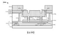
如圖29的剖面圖2900所示,在接合墊開口2402中形成接合墊層2002。在一些實施例中,可例如藉由無電式鍍覆、電鍍、濺射或另一合適的沉積製程來沉積及/或生長接合墊層2002。在另外的實施例中,接合墊層2002可例如為或包括鋁、銅、鋁銅等。在另外的實施例中,接合墊層2002可包括與導通孔106及/或導電線108相同的材料。As shown in the
如圖30的剖面圖3000所示,對接合墊層(圖29的接合墊層2002)執行第四蝕刻製程,藉此界定接合墊116。接合墊116與第一絕緣層802和第二絕緣層804的側壁橫向偏移距離d2。在一些實施例中,距離d2是非零的。在另外的實施例中,第四蝕刻製程包含:在接合墊層(圖29的接合墊層2002)上方形成掩蔽層(未示出);使接合墊層(圖29的接合墊層2002)的未掩蔽區暴露於一種或多種蝕刻劑,藉此界定接合墊116;以及執行去除製程以去除掩蔽層。As shown in the
圖31示出根據本公開的形成積體電路的第二方法3100。雖然將第二方法3100示出及/或描述為一系列動作或事件,但應瞭解,所述方法不限於所示出的次序或動作。因此,在一些實施例中,動作可以與所示出的不同次序進行及/或可同時進行。另外,在一些實施例中,所示出的動作或事件可細分成多個動作或事件,其可與其它動作或子動作在不同時間進行或同時進行。在一些實施例中,可省略一些所示出的動作或事件,並且可包含其它未示出的動作或事件。FIG. 31 shows a
在動作3102處,在半導體基板的前側上形成淺溝槽隔離(STI)結構。圖9示出對應於動作3102的一些實施例的剖面圖900。At
在動作3104處,在半導體基板中形成接合墊隔離結構。接合墊隔離結構從半導體基板的前側延伸到半導體基板的背側。圖10和圖11示出對應於動作3104的一些實施例的剖面圖1000和剖面圖1100。At
在動作3106處,在半導體基板的前側上形成內連線結構。內連線結構包含上部導電線層。圖12示出對應於動作3106的一些實施例的剖面圖1200。At
在動作3108處,在半導體基板的背側上方形成介電結構。圖14示出對應於動作3108的一些實施例的剖面圖1400。At
在動作3110處,使介電結構和半導體基板圖案化,藉此界定接合墊開口。圖24示出對應於動作3110的一些實施例的剖面圖2400。At
在動作3112處,在介電結構和半導體基板上方形成第一絕緣層。第一絕緣層對接合墊開口進行加襯。圖25示出對應於動作3112的一些實施例的剖面圖2500。At
在動作3114處,使第一絕緣層和半導體基板圖案化,藉此擴大接合墊開口且暴露出STI結構的上表面。圖26示出對應於動作3114的一些實施例的剖面圖2600。At
在動作3116處,在第一絕緣層和STI結構上方形成第二絕緣層。圖27示出對應於動作3116的一些實施例的剖面圖2700。At
在動作3118處,使第一絕緣層和第二絕緣層、STI結構以及內連線結構圖案化,藉此暴露出上部導電線層的上表面且擴大接合墊開口。圖28示出對應於動作3118的一些實施例的剖面圖2800。At
在動作3120處,在接合墊開口中形成接合墊。接合墊隔離結構圍繞接合墊連續延伸。圖29和圖30示出對應於動作3120的一些實施例的剖面圖2900和剖面圖3000。At
圖32到圖38示出根據本公開的各個方面的形成包含接合墊隔離結構的積體晶片的第三方法的一些實施例的剖面圖3200到剖面圖3800,所述接合墊隔離結構包圍接合墊。雖參照第三方法描述圖32到圖38中所示的剖面圖3200到剖面圖3800,但應瞭解,圖32到圖38中所示的結構不限於所述方法而實際上可單獨獨立於所述方法。雖然將圖32到圖38描述為一系列動作,但應瞭解,這些動作不限於所述動作的次序可在其它實施例中更改,並且所公開的方法還適用於其它結構。在其它實施例中,示出及/或描述的一些動作可完全或部分地省略。32 to 38 show
如圖32的剖面圖3200所示,在半導體基板110的前側110fs上形成淺溝槽隔離(STI)結構112。在一些實施例中,如圖9到圖11中所示出及/或描述形成圖32的STI結構112。As shown in the
如圖33的剖面圖3300所示,在半導體基板110的前側110fs上形成內連線結構104。內連線結構104接合到載體基板102,並且在半導體基板110的背側110bs上方形成介電結構118。另外,在介電結構118上方形成介電保護層1202。在一些實施例中,如圖12到圖14中所示出及/或描述形成圖33的結構。As shown in the
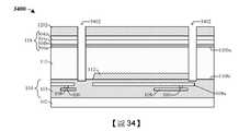
如圖34的剖面圖3400所示,對介電保護層1202、介電結構118以及半導體基板110執行蝕刻製程,藉此形成接合墊隔離開口3402。在一些實施例中,蝕刻製程可去除內連線介電結構103的至少一部分。在一些實施例中,蝕刻製程可包含執行濕式蝕刻製程、乾式蝕刻製程或另一合適的蝕刻製程。在一些實施例中,蝕刻製程包含:在介電保護層1202上方形成掩蔽層(未示出);使介電保護層1202的未掩蔽區和底層暴露於一種或多種蝕刻劑,藉此界定接合墊隔離開口3402;以及執行去除製程以去除掩蔽層。As shown in the
如圖35的剖面圖3500所示,在介電保護層1202上方和接合墊隔離開口(圖34的接合墊隔離開口3402)內形成第一DTI層3502和第二DTI層3504。在一些實施例中,省略第一DTI層3502,並且第二DTI層3504完全填充接合墊隔離開口(圖34的接合墊隔離開口3402)。在一些實施例中,第一DTI層3502可例如為或包括氧化物(如二氧化矽、另一合適的氧化物等)及/或可形成為約15,000埃的厚度。在另外的實施例中,第二DTI層3504可例如為或包括氮氧化矽、另一合適的介電材料等及/或可形成為約700埃的厚度。As shown in the
如圖36的剖面圖3600所示,對第一DTI層及/或第二DTI層(圖35的第一DTI層3502、第二DTI層3504)執行平坦化製程,藉此界定接合墊隔離結構114。接合墊隔離結構114可包括第一接合墊隔離層114a及/或第二接合墊隔離層114b。在一些實施例中,平坦化製程包含:對第一DTI層和第二DTI層(圖35的第一DTI層3502、第二DTI層3504)以及介電保護層1202執行化學機械平坦化(CMP)。在另外的實施例中,平坦化製程可減小介電保護層1202的厚度。As shown in the
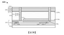
如圖37的剖面圖3700所示,接合墊116形成於半導體基板110中且由接合墊隔離結構114連續包圍。在一些實施例中,如圖15到圖21中所示出及/或描述形成圖37的結構。在另外的實施例中,如圖24到圖30中所示出及/或描述形成接合墊116。可藉由省略第一DTI層(圖35的第一DTI層3502)來形成圖37的結構,在所述結構中,接合墊隔離結構114包括第一接合墊隔離層114a。在一些實施例中,第一接合墊隔離層114a可例如為或包括二氧化矽、另一合適的氧化物等。As shown in the
如圖38的剖面圖3800所示,接合墊116形成於半導體基板110中且由接合墊隔離結構114連續包圍。在一些實施例中,如圖15到圖21中所示出及/或描述形成圖38的結構。在另外的實施例中,如圖24到圖30中所示出及/或描述形成接合墊116。接合墊隔離結構114包括第一接合墊隔離層114a和第二接合墊隔離層114b。在一些實施例中,第一接合墊隔離層114a可例如為或包括二氧化矽、另一合適的氧化物等。在另外的實施例中,第二接合墊隔離層114b可例如為或包括氮氧化矽、另一合適的介電材料等。As shown in the
圖39示出根據本公開的形成積體電路的第三方法3900。雖然將第三方法3900示出及/或描述為一系列動作或事件,但應瞭解,所述方法不限於所示出的次序或動作。因此,在一些實施例中,動作可以與所示出的不同次序進行及/或可同時進行。另外,在一些實施例中,所示出的動作或事件可細分成多個動作或事件,其可與其它動作或子動作在不同時間進行或同時進行。在一些實施例中,可省略一些所示出的動作或事件,並且可包含其它未示出的動作或事件。FIG. 39 shows a
在動作3902處,在半導體基板的前側上形成淺溝槽隔離(STI)結構。圖32示出對應於動作3902的一些實施例的剖面圖3200。At
在動作3904處,在半導體基板的前側上形成內連線結構。內連線結構包含上部導電線層。圖33示出對應於動作3904的一些實施例的剖面圖3300。At
在動作3906處,在半導體基板的背側上方形成介電結構。圖33示出對應於動作3906的一些實施例的剖面圖3300。At
在動作3908處,在半導體基板和介電結構中形成接合墊隔離結構。接合墊隔離結構從半導體基板的前側延伸到半導體基板的背側。圖35和圖36示出對應於動作3908的一些實施例的剖面圖3500和剖面圖3600。At
在動作3910處,在半導體基板中形成接合墊。接合墊隔離結構圍繞接合墊連續延伸。圖37和圖38示出對應於動作3910的一些實施例的剖面圖3700和剖面圖3800。At
因此,在一些實施例中,本公開涉及一種與裝置區橫向偏移的接合墊區。所述接合墊區包含延伸穿過半導體基板到內連線結構的接合墊。接合墊隔離結構設置在半導體基板內且連續包圍接合墊的外部側壁。Therefore, in some embodiments, the present disclosure relates to a bond pad region that is laterally offset from the device region. The bonding pad region includes bonding pads extending through the semiconductor substrate to the interconnect structure. The bonding pad isolation structure is arranged in the semiconductor substrate and continuously surrounds the outer sidewall of the bonding pad.
在一些實施例中,本公開提供一種半導體裝置結構,所述半導體裝置結構包含:半導體基板,具有背側表面和與所述背側表面相對的前側表面;接合墊,延伸穿過半導體基板;以及接合墊隔離結構,設置在半導體基板內,其中所述接合墊隔離結構從半導體基板的前側表面延伸到背側表面,以及其中接合墊隔離結構圍繞接合墊連續延伸。In some embodiments, the present disclosure provides a semiconductor device structure including: a semiconductor substrate having a backside surface and a frontside surface opposite to the backside surface; bonding pads extending through the semiconductor substrate; and The bonding pad isolation structure is arranged in the semiconductor substrate, wherein the bonding pad isolation structure extends from the front side surface to the back side surface of the semiconductor substrate, and the bonding pad isolation structure continuously extends around the bonding pad.
在一些實施例中,所述接合墊直接接觸所述半導體基板的上表面及側壁。在一些實施例中,所述接合墊包括導電主體以及導電突部,導電主體直接接觸所述半導體基板的上表面,其中所述導電主體的頂表面豎直地位於所述半導體基板的所述背側表面上方,導電突部從所述導電主體延伸到所述半導體基板的所述前側表面下方的點,其中所述導電突部直接接觸所述半導體基板的側壁,以及所述導電突部的頂表面與所述半導體基板的所述上表面對準。在一些實施例中,半導體裝置結構更包括多個光偵測器以及介電結構,多個光偵測器設置在所述半導體基板內,其中所述光偵測器與所述接合墊隔離結構橫向偏移非零距離,介電結構設置在所述半導體基板的所述背側表面上方,其中所述介電結構的所述頂表面與所述接合墊的頂表面對準。在一些實施例中,半導體裝置結構更包括電晶體,電晶體在所述光偵測器與所述接合墊隔離結構之間橫向設置在所述半導體基板的所述前側表面上。在一些實施例中,半導體裝置結構更包括內連線結構,內連線結構沿著所述半導體基板的所述前側表面設置,其中所述內連線結構包含設置在內連線介電結構內的導電線層,所述接合墊延伸穿過所述內連線介電結構且接觸所述導電線層。在一些實施例中,所述接合墊隔離結構的底表面設置在所述半導體基板的所述前側表面下方,所述接合墊隔離結構延伸到所述內連線介電結構中。在一些實施例中,所述接合墊隔離結構具有比所述半導體基板的高度更大的高度。在一些實施例中,半導體裝置結構更包括第一絕緣層以及第二絕緣層,第一絕緣層沿著所述半導體基板的第一相對側壁及所述半導體基板的上表面設置,其中所述接合墊的下表面直接接觸所述第一絕緣層的上表面,所述第一相對側壁從所述背側表面連續延伸到所述半導體基板的所述上表面,第二絕緣層從所述半導體基板的所述上表面延伸到所述半導體基板的所述前側表面上方的點,其中所述第二絕緣層將所述接合墊與所述半導體基板隔開。在一些實施例中,所述接合墊的上部側壁與所述第一絕緣層的側壁橫向偏移,其中所述第二絕緣層沿著所述接合墊的下部側壁從所述接合墊的所述下表面延伸到所述前側表面上方的所述點。In some embodiments, the bonding pad directly contacts the upper surface and sidewalls of the semiconductor substrate. In some embodiments, the bonding pad includes a conductive body and a conductive protrusion, the conductive body directly contacts the upper surface of the semiconductor substrate, and the top surface of the conductive body is vertically located on the back of the semiconductor substrate. Side tableAbove the surface, a conductive protrusion extends from the conductive body to a point below the front surface of the semiconductor substrate, wherein the conductive protrusion directly contacts the sidewall of the semiconductor substrate, and the top surface of the conductive protrusion Align with the upper surface of the semiconductor substrate. In some embodiments, the semiconductor device structure further includes a plurality of photodetectors and a dielectric structure, the plurality of photodetectors are disposed in the semiconductor substrate, wherein the photodetector and the bonding pad isolation structure The lateral offset is non-zero distance, a dielectric structure is disposed above the backside surface of the semiconductor substrate, wherein the top surface of the dielectric structure is aligned with the top surface of the bonding pad. In some embodiments, the semiconductor device structure further includes a transistor, and the transistor is laterally disposed on the front surface of the semiconductor substrate between the photodetector and the bonding pad isolation structure. In some embodiments, the semiconductor device structure further includes an interconnect structure disposed along the front side surface of the semiconductor substrate, wherein the interconnect structure includes an interconnect dielectric structure The conductive wire layer, the bonding pad extends through the interconnect dielectric structure and contacts the conductive wire layer. In some embodiments, the bottom surface of the bonding pad isolation structure is disposed below the front side surface of the semiconductor substrate, and the bonding pad isolation structure extends into the interconnect dielectric structure. In some embodiments, the bond pad isolation structure has a height greater than the height of the semiconductor substrate. In some embodiments, the semiconductor device structure further includes a first insulating layer and a second insulating layer. The first insulating layer is disposed along the first opposite sidewalls of the semiconductor substrate and the upper surface of the semiconductor substrate, wherein the bonding The lower surface of the pad directly contacts the upper surface of the first insulating layer, the first opposite sidewalls continuously extend from the backside surface to the upper surface of the semiconductor substrate, and the second insulating layerA layer extends from the upper surface of the semiconductor substrate to a point above the front side surface of the semiconductor substrate, wherein the second insulating layer separates the bonding pad from the semiconductor substrate. In some embodiments, the upper sidewall of the bonding pad is laterally offset from the sidewall of the first insulating layer, and the second insulating layer is moved from the sidewall of the bonding pad along the lower sidewall of the bonding pad. The lower surface extends to the point above the front side surface.
在一些實施例中,本公開提供一種半導體裝置結構,所述半導體裝置結構包含:半導體基板,上覆於載體基板,其中光偵測器設置在半導體基板中;內連線結構,設置在半導體基板與載體基板之間,其中上部導電線層設置在內連線結構中;接合墊,延伸穿過半導體基板到內連線結構,其中所述接合墊接觸上部導電線層且具有設置在半導體基板上方的頂表面,其中接合墊與光偵測器橫向偏移;以及接合墊隔離結構,設置在半導體基板內,其中所述接合墊隔離結構連續環繞接合墊的外部側壁。In some embodiments, the present disclosure provides a semiconductor device structure. The semiconductor device structure includes: a semiconductor substrate overlying a carrier substrate, wherein a photodetector is provided in the semiconductor substrate; an interconnect structure is provided on the semiconductor substrate Between the upper conductive wire layer and the carrier substrate, the upper conductive wire layer is arranged in the interconnect structure; the bonding pad extends through the semiconductor substrate to the interconnect structure, wherein the bonding pad is in contact with the upper conductive wire layer and is arranged above the semiconductor substrate The top surface of the bonding pad and the photodetector are laterally offset; and the bonding pad isolation structure is arranged in the semiconductor substrate, wherein the bonding pad isolation structure continuously surrounds the outer sidewall of the bonding pad.
在一些實施例中,所述接合墊隔離結構從所述半導體基板的所述頂表面延伸到所述內連線結構。在一些實施例中,所述接合墊隔離結構的內部側壁與所述接合墊的所述外部側壁橫向偏移非零距離。在一些實施例中,半導體裝置結構更包括介電結構以及柵格結構,介電結構上覆於所述半導體基板的頂表面,其中所述介電結構的頂表面沿著大致上筆直的線設置,柵格結構上覆於所述光偵測器,所述介電結構設置在所述柵格結構與所述半導體基板之間,並且所述接合墊的頂表面沿著所述大致上筆直的線設置。在一些實施例中,半導體裝置結構更包括淺溝槽隔離結構,淺溝槽隔離結構設置在所述半導體基板內且沿著所述內連線結構的上表面設置,所述接合墊包括導電突部,所述導電突部延伸穿過所述淺溝槽隔離結構到所述上部導電線層。在一些實施例中,所述接合墊隔離結構包括與所述淺溝槽隔離結構相同的材料。在一些實施例中,所述淺溝槽隔離結構橫向設置在所述接合墊隔離結構的內部側壁之間,以及所述淺溝槽隔離結構與所述接合墊隔離結構的所述內部側壁橫向偏移非零距離。In some embodiments, the bond pad isolation structure extends from the top surface of the semiconductor substrate to the interconnect structure. In some embodiments, the inner side wall of the bonding pad isolation structure is laterally offset from the outer side wall of the bonding pad by a non-zero distance. In some embodiments, the semiconductor device structure further includes a dielectric structure and a grid structure, the dielectric structure is overlying the top surface of the semiconductor substrate, wherein the top surface of the dielectric structure is arranged along a substantially straight line , The grid structure is overlying the photodetector, the dielectric structure is disposed between the grid structure and the semiconductor substrate, and the top surface of the bonding pad is along the substantially straight Stringset up. In some embodiments, the semiconductor device structure further includes a shallow trench isolation structure, the shallow trench isolation structure is disposed in the semiconductor substrate and is disposed along the upper surface of the interconnect structure, and the bonding pad includes conductive protrusions. Part, the conductive protrusion extends through the shallow trench isolation structure to the upper conductive line layer. In some embodiments, the bond pad isolation structure includes the same material as the shallow trench isolation structure. In some embodiments, the shallow trench isolation structure is laterally disposed between the inner sidewalls of the bonding pad isolation structure, and the shallow trench isolation structure is laterally offset from the inner sidewalls of the bonding pad isolation structure. Shift non-zero distance.
在一些實施例中,本公開提供一種用於形成半導體裝置結構的方法,所述方法包含:在半導體基板中形成接合墊隔離結構,其中所述接合墊隔離結構從半導體基板的前側表面延伸到背側表面;在半導體基板的前側表面上形成內連線結構,其中所述內連線結構包含導電線層;使半導體基板的前側表面圖案化以界定接合墊開口且暴露出導電線層的上表面,其中所述接合墊開口橫向設置在接合墊隔離結構的內部側壁之間;以及在接合墊開口中形成接合墊,其中所述接合墊從半導體基板延伸到導電線層,以及其中接合墊隔離結構連續環繞接合墊。In some embodiments, the present disclosure provides a method for forming a semiconductor device structure, the method comprising: forming a bonding pad isolation structure in a semiconductor substrate, wherein the bonding pad isolation structure extends from a front side surface of the semiconductor substrate to a back surface of the semiconductor substrate. Side surface; forming an interconnect structure on the front surface of the semiconductor substrate, wherein the interconnect structure includes a conductive wire layer; patterning the front surface of the semiconductor substrate to define the bonding pad opening and expose the upper surface of the conductive wire layer , Wherein the bonding pad opening is laterally arranged between the inner sidewalls of the bonding pad isolation structure; and forming a bonding pad in the bonding pad opening, wherein the bonding pad extends from the semiconductor substrate to the conductive line layer, and wherein the bonding pad isolation structure Continuously surround the bonding pad.
在一些實施例中,形成所述接合墊包括在所述半導體基板及所述內連線結構上方形成接合墊層,使所述接合墊層填充所述接合墊開口且直接接觸所述半導體基板,使所述接合墊層圖案化以界定所述接合墊,其中所述半導體基板包括上部側壁和在所述上部側壁之下的下部側壁,所述上部側壁及所述下部側壁界定所述接合墊開口,所述接合墊與所述上部側壁橫向偏移非零距離且直接接觸所述下部側壁。在一些實施例中,用於形成半導體裝置結構的方法更包括在所述半導體基板的所述前側表面上形成淺溝槽隔離結構,使所述淺溝槽隔離結構的外部側壁橫向地位於所述接合墊隔離結構的內部側壁之間,其中所述淺溝槽隔離結構包括與所述接合墊隔離結構相同的材料。In some embodiments, forming the bonding pad includes forming a bonding pad layer over the semiconductor substrate and the interconnect structure, so that the bonding pad layer fills the bonding pad opening and directly contacts the semiconductor substrate, The bonding pad layer is patterned to define the bonding pad, wherein the semiconductor substrate includes an upper side wall and a lower side wall below the upper side wall, the upper side wall and the lower side wall definingThe bonding pad opens, and the bonding pad is laterally offset from the upper side wall by a non-zero distance and directly contacts the lower side wall. In some embodiments, the method for forming a semiconductor device structure further includes forming a shallow trench isolation structure on the front side surface of the semiconductor substrate, so that the outer sidewall of the shallow trench isolation structure is laterally located on the Between the inner sidewalls of the bonding pad isolation structure, wherein the shallow trench isolation structure includes the same material as the bonding pad isolation structure.
雖然本發明已以實施例揭露如上,然其並非用以界定本發明的實施例,任何所屬技術領域中具有通常知識者,在不脫離本發明實施例的精神和範圍內,當可作些許的更動與潤飾,故本發明的保護範圍當視後附的申請專利範圍所界定者為準。Although the present invention has been disclosed in the above embodiments, it is not used to define the embodiments of the present invention. Anyone with ordinary knowledge in the technical field can do a little bit without departing from the spirit and scope of the embodiments of the present invention. Modifications and modifications, so the scope of protection of the present invention shall be subject to those defined by the attached patent scope.
100:積體晶片100: Integrated chip
101a:裝置區101a: Installation area
101b:接合墊區101b: Bonding pad area
102:載體基板102: carrier substrate
103:內連線介電結構103: Inner connection dielectric structure
104:內連線結構104: Internal connection structure
106:導通孔106: Via
108:導電線108: Conductive thread
108a:上部導電線層108a: Upper conductive thread layer
110:半導體基板110: Semiconductor substrate
110bs:背側110bs: back side
110fs:前側110fs: front side
110is:內部側壁110is: inner side wall
110us:上表面110us: upper surface
112:淺溝槽隔離結構112: Shallow trench isolation structure
114:接合墊隔離結構114: Bonding pad isolation structure
116:接合墊116: Bonding pad
116a:上部導電主體116a: upper conductive body
116b:導電突部116b: conductive protrusion
116o:接墊開口116o: Pad opening
118:介電結構118: Dielectric structure
120:半導體裝置120: Semiconductor device
Fig.2:圖2Fig. 2: Fig. 2
h1、h2:高度h1 , h2 : height
Claims (10)
Translated fromChineseApplications Claiming Priority (2)
| Application Number | Priority Date | Filing Date | Title |
|---|---|---|---|
| US16/532,781 | 2019-08-06 | ||
| US16/532,781US10991667B2 (en) | 2019-08-06 | 2019-08-06 | Isolation structure for bond pad structure |
Publications (2)
| Publication Number | Publication Date |
|---|---|
| TW202121673A TW202121673A (en) | 2021-06-01 |
| TWI749682Btrue TWI749682B (en) | 2021-12-11 |
Family
ID=74357156
Family Applications (1)
| Application Number | Title | Priority Date | Filing Date |
|---|---|---|---|
| TW109126324ATWI749682B (en) | 2019-08-06 | 2020-08-04 | Isolation structure for bond pad structure and manufacturing method thereof |
Country Status (3)
| Country | Link |
|---|---|
| US (4) | US10991667B2 (en) |
| CN (1) | CN112349736B (en) |
| TW (1) | TWI749682B (en) |
Families Citing this family (11)
| Publication number | Priority date | Publication date | Assignee | Title |
|---|---|---|---|---|
| MY201172A (en)* | 2018-09-19 | 2024-02-08 | Intel Corp | Stacked through-silicon vias for multi-device packages |
| US10991667B2 (en)* | 2019-08-06 | 2021-04-27 | Taiwan Semiconductor Manufacturing Co., Ltd. | Isolation structure for bond pad structure |
| CN111312654B (en)* | 2019-12-02 | 2022-06-28 | 武汉新芯集成电路制造有限公司 | Semiconductor device and method of manufacturing the same |
| US12396272B2 (en)* | 2021-01-18 | 2025-08-19 | Taiwan Semiconductor Manufacturing Company, Ltd. | Stilted pad structure |
| US11764103B2 (en)* | 2021-05-07 | 2023-09-19 | Taiwan Semiconductor Manufacturing Company, Ltd. | Semiconductor feature and method for manufacturing the same |
| CN115458671A (en)* | 2021-06-09 | 2022-12-09 | 澜起科技股份有限公司 | Integrated refrigerating device based on Peltier effect and manufacturing method thereof |
| JP7621894B2 (en)* | 2021-06-16 | 2025-01-27 | キオクシア株式会社 | Semiconductor device and its manufacturing method |
| US12136627B2 (en)* | 2021-06-24 | 2024-11-05 | Taiwan Semiconductor Manufacturing Company, Ltd. | 3DIC structure for high voltage device on a SOI substrate |
| US12034027B2 (en)* | 2021-08-20 | 2024-07-09 | Omnivision Technologies, Inc. | Semiconductor device contact pad and method of contact pad fabrication |
| TWI802973B (en)* | 2021-08-24 | 2023-05-21 | 矽品精密工業股份有限公司 | Substrate structure |
| US20250255023A1 (en)* | 2024-02-05 | 2025-08-07 | Globalfoundries Singapore Pte. Ltd. | Structures including a photodetector and multiple deep trenches |
Citations (10)
| Publication number | Priority date | Publication date | Assignee | Title |
|---|---|---|---|---|
| US20150255495A1 (en)* | 2014-03-07 | 2015-09-10 | Samsung Electronics Co., Ltd. | Image sensor and method of manufacturing the same |
| US20150318323A1 (en)* | 2014-05-05 | 2015-11-05 | Semiconductor Components Industries, Llc | Image sensors with reduced stack height |
| TW201637191A (en)* | 2015-03-05 | 2016-10-16 | 豪威科技股份有限公司 | Aerogel coated image sensor and manufacturing method thereof |
| TW201639136A (en)* | 2015-04-17 | 2016-11-01 | 台灣積體電路製造股份有限公司 | Image sensing device and method of manufacturing same |
| TW201735334A (en)* | 2016-03-24 | 2017-10-01 | 台灣積體電路製造股份有限公司 | Back side illumination image sensor and forming method thereof |
| TW201735383A (en)* | 2016-03-17 | 2017-10-01 | 台灣積體電路製造股份有限公司 | Image sensor device and method of manufacturing same |
| TW201806137A (en)* | 2016-08-04 | 2018-02-16 | 力晶科技股份有限公司 | Image sensor and manufacturing method thereof |
| US20190148439A1 (en)* | 2017-11-14 | 2019-05-16 | Samsung Electronics Co., Ltd. | Image sensors |
| TW201926656A (en)* | 2017-11-28 | 2019-07-01 | 台灣積體電路製造股份有限公司 | Semiconductor image sensing device and method of forming same |
| TW201926662A (en)* | 2017-11-24 | 2019-07-01 | 台灣積體電路製造股份有限公司 | Method for forming image sensing device |
Family Cites Families (36)
| Publication number | Priority date | Publication date | Assignee | Title |
|---|---|---|---|---|
| KR20090033636A (en)* | 2007-10-01 | 2009-04-06 | 삼성전자주식회사 | Image sensor and its manufacturing method |
| JP5853351B2 (en)* | 2010-03-25 | 2016-02-09 | ソニー株式会社 | SEMICONDUCTOR DEVICE, SEMICONDUCTOR DEVICE MANUFACTURING METHOD, AND ELECTRONIC DEVICE |
| US8283754B2 (en) | 2010-08-13 | 2012-10-09 | Taiwan Semiconductor Manufacturing Company, Ltd. | Seal ring structure with metal pad |
| JP2012064709A (en)* | 2010-09-15 | 2012-03-29 | Sony Corp | Solid state image pick-up device and electronic device |
| US8847380B2 (en)* | 2010-09-17 | 2014-09-30 | Tessera, Inc. | Staged via formation from both sides of chip |
| JP2012227478A (en)* | 2011-04-22 | 2012-11-15 | Panasonic Corp | Solid state image pickup device |
| US8435824B2 (en)* | 2011-07-07 | 2013-05-07 | Taiwan Semiconductor Manufacturing Company, Ltd. | Backside illumination sensor having a bonding pad structure and method of making the same |
| US8987855B2 (en) | 2011-08-04 | 2015-03-24 | Taiwan Semiconductor Manufacturing Company, Ltd. | Pad structures formed in double openings in dielectric layers |
| US9013022B2 (en) | 2011-08-04 | 2015-04-21 | Taiwan Semiconductor Manufacturing Company, Ltd. | Pad structure including glue layer and non-low-k dielectric layer in BSI image sensor chips |
| US8502389B2 (en)* | 2011-08-08 | 2013-08-06 | Taiwan Semiconductor Manufacturing Company, Ltd. | CMOS image sensor and method for forming the same |
| JP2013187360A (en)* | 2012-03-08 | 2013-09-19 | Sony Corp | Solid-state image pickup device and electronic apparatus |
| US9219032B2 (en)* | 2012-07-09 | 2015-12-22 | Qualcomm Incorporated | Integrating through substrate vias from wafer backside layers of integrated circuits |
| US8866250B2 (en)* | 2012-09-05 | 2014-10-21 | Taiwan Semiconductor Manufacturing Company, Ltd. | Multiple metal film stack in BSI chips |
| US8796805B2 (en)* | 2012-09-05 | 2014-08-05 | Taiwan Semiconductor Manufacturing Company, Ltd. | Multiple metal film stack in BSI chips |
| JP6041607B2 (en)* | 2012-09-28 | 2016-12-14 | キヤノン株式会社 | Manufacturing method of semiconductor device |
| US10270003B2 (en) | 2012-12-04 | 2019-04-23 | Taiwan Semiconductor Manufacturing Company, Ltd. | Method and apparatus for CMOS sensor packaging |
| JP2015119154A (en)* | 2013-12-20 | 2015-06-25 | ソニー株式会社 | Solid state image pickup element, solid state image pickup element manufacturing method and electronic apparatus |
| US9679936B2 (en)* | 2014-02-27 | 2017-06-13 | Semiconductor Components Industries, Llc | Imaging systems with through-oxide via connections |
| US9281338B2 (en) | 2014-04-25 | 2016-03-08 | Taiwan Semiconductor Manufacturing Company, Ltd. | Semiconductor image sensor device having back side illuminated image sensors with embedded color filters |
| CN104362162A (en)* | 2014-09-30 | 2015-02-18 | 武汉新芯集成电路制造有限公司 | Image sensor with landfill type color filter and manufacture method thereof |
| TW201637190A (en)* | 2015-03-25 | 2016-10-16 | Sony Corp | Solid-state imaging device and electronic device |
| US10217783B2 (en)* | 2015-04-08 | 2019-02-26 | Semiconductor Components Industries, Llc | Methods for forming image sensors with integrated bond pad structures |
| US9536810B1 (en)* | 2015-06-12 | 2017-01-03 | Taiwan Semiconductor Manufacturing Co., Ltd. | Flat pad structure for integrating complementary metal-oxide-semiconductor (CMOS) image sensor processes |
| US9704827B2 (en) | 2015-06-25 | 2017-07-11 | Taiwan Semiconductor Manufacturing Co., Ltd. | Hybrid bond pad structure |
| KR102437163B1 (en)* | 2015-08-07 | 2022-08-29 | 삼성전자주식회사 | Semiconductor device |
| US9881884B2 (en)* | 2015-08-14 | 2018-01-30 | Taiwan Semiconductor Manufacturing Co., Ltd. | Semiconductor device structure and method for forming the same |
| US10833119B2 (en) | 2015-10-26 | 2020-11-10 | Taiwan Semiconductor Manufacturing Co., Ltd. | Pad structure for front side illuminated image sensor |
| US9847359B2 (en)* | 2015-11-17 | 2017-12-19 | Semiconductor Components Industries, Llc | Image sensors with improved surface planarity |
| US10038025B2 (en) | 2015-12-29 | 2018-07-31 | Taiwan Semiconductor Manufacturing Co., Ltd. | Via support structure under pad areas for BSI bondability improvement |
| US10109666B2 (en) | 2016-04-13 | 2018-10-23 | Taiwan Semiconductor Manufacturing Co., Ltd. | Pad structure for backside illuminated (BSI) image sensors |
| FR3056332A1 (en) | 2016-09-21 | 2018-03-23 | Stmicroelectronics (Grenoble 2) Sas | DEVICE COMPRISING A 2D IMAGE SENSOR AND A DEPTH SENSOR |
| US10147754B2 (en)* | 2017-02-22 | 2018-12-04 | Omnivision Technologies, Inc. | Backside illuminated image sensor with improved contact area |
| US10249675B1 (en)* | 2017-09-18 | 2019-04-02 | OmniVision Technolgies, Inc. | Backside illuminated image sensor with self-aligned metal pad structures |
| US11164903B2 (en)* | 2019-05-24 | 2021-11-02 | Taiwan Semiconductor Manufacturing Co., Ltd. | Image sensor with pad structure |
| US10991667B2 (en)* | 2019-08-06 | 2021-04-27 | Taiwan Semiconductor Manufacturing Co., Ltd. | Isolation structure for bond pad structure |
| US11217547B2 (en)* | 2019-09-03 | 2022-01-04 | Taiwan Semiconductor Manufacturing Company, Ltd. | Bond pad structure with reduced step height and increased electrical isolation |
- 2019
- 2019-08-06USUS16/532,781patent/US10991667B2/enactiveActive
- 2020
- 2020-02-27CNCN202010124157.0Apatent/CN112349736B/enactiveActive
- 2020-08-04TWTW109126324Apatent/TWI749682B/enactive
- 2021
- 2021-04-21USUS17/236,360patent/US11694979B2/enactiveActive
- 2023
- 2023-05-17USUS18/318,887patent/US12400984B2/enactiveActive
- 2024
- 2024-05-10USUS18/660,276patent/US12424577B2/enactiveActive
Patent Citations (10)
| Publication number | Priority date | Publication date | Assignee | Title |
|---|---|---|---|---|
| US20150255495A1 (en)* | 2014-03-07 | 2015-09-10 | Samsung Electronics Co., Ltd. | Image sensor and method of manufacturing the same |
| US20150318323A1 (en)* | 2014-05-05 | 2015-11-05 | Semiconductor Components Industries, Llc | Image sensors with reduced stack height |
| TW201637191A (en)* | 2015-03-05 | 2016-10-16 | 豪威科技股份有限公司 | Aerogel coated image sensor and manufacturing method thereof |
| TW201639136A (en)* | 2015-04-17 | 2016-11-01 | 台灣積體電路製造股份有限公司 | Image sensing device and method of manufacturing same |
| TW201735383A (en)* | 2016-03-17 | 2017-10-01 | 台灣積體電路製造股份有限公司 | Image sensor device and method of manufacturing same |
| TW201735334A (en)* | 2016-03-24 | 2017-10-01 | 台灣積體電路製造股份有限公司 | Back side illumination image sensor and forming method thereof |
| TW201806137A (en)* | 2016-08-04 | 2018-02-16 | 力晶科技股份有限公司 | Image sensor and manufacturing method thereof |
| US20190148439A1 (en)* | 2017-11-14 | 2019-05-16 | Samsung Electronics Co., Ltd. | Image sensors |
| TW201926662A (en)* | 2017-11-24 | 2019-07-01 | 台灣積體電路製造股份有限公司 | Method for forming image sensing device |
| TW201926656A (en)* | 2017-11-28 | 2019-07-01 | 台灣積體電路製造股份有限公司 | Semiconductor image sensing device and method of forming same |
Also Published As
| Publication number | Publication date |
|---|---|
| US12400984B2 (en) | 2025-08-26 |
| CN112349736B (en) | 2025-03-11 |
| US12424577B2 (en) | 2025-09-23 |
| US10991667B2 (en) | 2021-04-27 |
| US20230290749A1 (en) | 2023-09-14 |
| US11694979B2 (en) | 2023-07-04 |
| US20210242153A1 (en) | 2021-08-05 |
| TW202121673A (en) | 2021-06-01 |
| US20240290740A1 (en) | 2024-08-29 |
| CN112349736A (en) | 2021-02-09 |
| US20210043593A1 (en) | 2021-02-11 |
Similar Documents
| Publication | Publication Date | Title |
|---|---|---|
| TWI749682B (en) | Isolation structure for bond pad structure and manufacturing method thereof | |
| TWI714329B (en) | Semiconductor structure and method of forming same | |
| US20230378139A1 (en) | 3DIC Interconnect Apparatus and Method | |
| US10157891B2 (en) | 3DIC interconnect apparatus and method | |
| US9960200B1 (en) | Selective deposition and planarization for a CMOS image sensor | |
| TWI688085B (en) | Semiconductor image sensor devices and methods of forming the same | |
| CN106252323A (en) | Flat Pad Structure for Integrated Complementary Metal Oxide Semiconductor (CMOS) Image Sensor Process | |
| CN117393574B (en) | Semiconductor structure and manufacturing method thereof | |
| KR20100028623A (en) | Imagers with contact plugs extending through the substrates thereof and imager fabrication methods | |
| TWI717795B (en) | Image sensor and method for forming the same | |
| US20220310692A1 (en) | Charge release layer to remove charge carriers from dielectric grid structures in image sensors | |
| KR100855405B1 (en) | Manufacturing Method of Image Sensor | |
| KR101038807B1 (en) | Image sensor and manufacturing method | |
| KR100856948B1 (en) | Image sensor manufacturing method | |
| CN101136424A (en) | Image sensor and its manufacturing method | |
| TWI870988B (en) | Image sensor integrated chip and method of forming the same | |
| TW201810632A (en) | Color filter device and forming method |