TWI748481B - Semiconductor device and method of forming the same - Google Patents
Semiconductor device and method of forming the sameDownload PDFInfo
- Publication number
- TWI748481B TWI748481BTW109117798ATW109117798ATWI748481BTW I748481 BTWI748481 BTW I748481BTW 109117798 ATW109117798 ATW 109117798ATW 109117798 ATW109117798 ATW 109117798ATW I748481 BTWI748481 BTW I748481B
- Authority
- TW
- Taiwan
- Prior art keywords
- semiconductor substrate
- vertical
- transfer gate
- front side
- trench isolation
- Prior art date
Links
- 239000004065semiconductorSubstances0.000titleclaimsabstractdescription138
- 238000000034methodMethods0.000titleclaimsdescription29
- 239000000758substrateSubstances0.000claimsabstractdescription157
- 238000002955isolationMethods0.000claimsabstractdescription111
- 238000009792diffusion processMethods0.000claimsdescription13
- 239000007772electrode materialSubstances0.000claimsdescription6
- 238000000059patterningMethods0.000claimsdescription4
- VYPSYNLAJGMNEJ-UHFFFAOYSA-NSilicium dioxideChemical compoundO=[Si]=OVYPSYNLAJGMNEJ-UHFFFAOYSA-N0.000description16
- 230000009471actionEffects0.000description14
- 239000003989dielectric materialSubstances0.000description14
- 238000010586diagramMethods0.000description11
- 230000003287optical effectEffects0.000description11
- 230000008569processEffects0.000description11
- 238000005468ion implantationMethods0.000description8
- 235000012239silicon dioxideNutrition0.000description8
- 239000000377silicon dioxideSubstances0.000description8
- 238000005530etchingMethods0.000description7
- 239000000463materialSubstances0.000description6
- 229920002120photoresistant polymerPolymers0.000description6
- 229910052751metalInorganic materials0.000description5
- 239000002184metalSubstances0.000description5
- 229910052581Si3N4Inorganic materials0.000description4
- 230000003213activating effectEffects0.000description4
- 239000006117anti-reflective coatingSubstances0.000description4
- 239000004020conductorSubstances0.000description4
- 230000010354integrationEffects0.000description4
- 238000001459lithographyMethods0.000description4
- HQVNEWCFYHHQES-UHFFFAOYSA-Nsilicon nitrideChemical compoundN12[Si]34N5[Si]62N3[Si]51N64HQVNEWCFYHHQES-UHFFFAOYSA-N0.000description4
- 125000006850spacer groupChemical group0.000description4
- 230000007704transitionEffects0.000description4
- RYGMFSIKBFXOCR-UHFFFAOYSA-NCopperChemical compound[Cu]RYGMFSIKBFXOCR-UHFFFAOYSA-N0.000description3
- 229910052802copperInorganic materials0.000description3
- 239000010949copperSubstances0.000description3
- 229910052782aluminiumInorganic materials0.000description2
- XAGFODPZIPBFFR-UHFFFAOYSA-NaluminiumChemical compound[Al]XAGFODPZIPBFFR-UHFFFAOYSA-N0.000description2
- WPPDFTBPZNZZRP-UHFFFAOYSA-Naluminum copperChemical compound[Al].[Cu]WPPDFTBPZNZZRP-UHFFFAOYSA-N0.000description2
- 239000000969carrierSubstances0.000description2
- 230000008859changeEffects0.000description2
- 238000005229chemical vapour depositionMethods0.000description2
- 238000005336crackingMethods0.000description2
- 238000000151depositionMethods0.000description2
- 238000005137deposition processMethods0.000description2
- 239000012212insulatorSubstances0.000description2
- 150000002739metalsChemical class0.000description2
- 229910021420polycrystalline siliconInorganic materials0.000description2
- 229920005591polysiliconPolymers0.000description2
- 230000005855radiationEffects0.000description2
- HBMJWWWQQXIZIP-UHFFFAOYSA-Nsilicon carbideChemical compound[Si+]#[C-]HBMJWWWQQXIZIP-UHFFFAOYSA-N0.000description2
- 229910010271silicon carbideInorganic materials0.000description2
- WFKWXMTUELFFGS-UHFFFAOYSA-NtungstenChemical compound[W]WFKWXMTUELFFGS-UHFFFAOYSA-N0.000description2
- 229910052721tungstenInorganic materials0.000description2
- 239000010937tungstenSubstances0.000description2
- 238000007740vapor depositionMethods0.000description2
- 238000013459approachMethods0.000description1
- 230000015572biosynthetic processEffects0.000description1
- 230000000295complement effectEffects0.000description1
- 230000008878couplingEffects0.000description1
- 238000010168coupling processMethods0.000description1
- 238000005859coupling reactionMethods0.000description1
- 239000013078crystalSubstances0.000description1
- 230000003247decreasing effectEffects0.000description1
- 238000001514detection methodMethods0.000description1
- 238000001312dry etchingMethods0.000description1
- 230000000694effectsEffects0.000description1
- 238000011065in-situ storageMethods0.000description1
- 238000004519manufacturing processMethods0.000description1
- 229910044991metal oxideInorganic materials0.000description1
- 150000004706metal oxidesChemical class0.000description1
- 229910021421monocrystalline siliconInorganic materials0.000description1
- 230000004044responseEffects0.000description1
- 230000035945sensitivityEffects0.000description1
- 238000004528spin coatingMethods0.000description1
- 238000006467substitution reactionMethods0.000description1
- 238000005019vapor deposition processMethods0.000description1
Images


Classifications
- H—ELECTRICITY
- H10—SEMICONDUCTOR DEVICES; ELECTRIC SOLID-STATE DEVICES NOT OTHERWISE PROVIDED FOR
- H10F—INORGANIC SEMICONDUCTOR DEVICES SENSITIVE TO INFRARED RADIATION, LIGHT, ELECTROMAGNETIC RADIATION OF SHORTER WAVELENGTH OR CORPUSCULAR RADIATION
- H10F39/00—Integrated devices, or assemblies of multiple devices, comprising at least one element covered by group H10F30/00, e.g. radiation detectors comprising photodiode arrays
- H10F39/80—Constructional details of image sensors
- H10F39/813—Electronic components shared by multiple pixels, e.g. one amplifier shared by two pixels
- H—ELECTRICITY
- H10—SEMICONDUCTOR DEVICES; ELECTRIC SOLID-STATE DEVICES NOT OTHERWISE PROVIDED FOR
- H10F—INORGANIC SEMICONDUCTOR DEVICES SENSITIVE TO INFRARED RADIATION, LIGHT, ELECTROMAGNETIC RADIATION OF SHORTER WAVELENGTH OR CORPUSCULAR RADIATION
- H10F39/00—Integrated devices, or assemblies of multiple devices, comprising at least one element covered by group H10F30/00, e.g. radiation detectors comprising photodiode arrays
- H10F39/80—Constructional details of image sensors
- H10F39/807—Pixel isolation structures
- H—ELECTRICITY
- H10—SEMICONDUCTOR DEVICES; ELECTRIC SOLID-STATE DEVICES NOT OTHERWISE PROVIDED FOR
- H10F—INORGANIC SEMICONDUCTOR DEVICES SENSITIVE TO INFRARED RADIATION, LIGHT, ELECTROMAGNETIC RADIATION OF SHORTER WAVELENGTH OR CORPUSCULAR RADIATION
- H10F39/00—Integrated devices, or assemblies of multiple devices, comprising at least one element covered by group H10F30/00, e.g. radiation detectors comprising photodiode arrays
- H10F39/011—Manufacture or treatment of image sensors covered by group H10F39/12
- H10F39/014—Manufacture or treatment of image sensors covered by group H10F39/12 of CMOS image sensors
- H—ELECTRICITY
- H10—SEMICONDUCTOR DEVICES; ELECTRIC SOLID-STATE DEVICES NOT OTHERWISE PROVIDED FOR
- H10F—INORGANIC SEMICONDUCTOR DEVICES SENSITIVE TO INFRARED RADIATION, LIGHT, ELECTROMAGNETIC RADIATION OF SHORTER WAVELENGTH OR CORPUSCULAR RADIATION
- H10F39/00—Integrated devices, or assemblies of multiple devices, comprising at least one element covered by group H10F30/00, e.g. radiation detectors comprising photodiode arrays
- H10F39/011—Manufacture or treatment of image sensors covered by group H10F39/12
- H10F39/018—Manufacture or treatment of image sensors covered by group H10F39/12 of hybrid image sensors
- H—ELECTRICITY
- H10—SEMICONDUCTOR DEVICES; ELECTRIC SOLID-STATE DEVICES NOT OTHERWISE PROVIDED FOR
- H10F—INORGANIC SEMICONDUCTOR DEVICES SENSITIVE TO INFRARED RADIATION, LIGHT, ELECTROMAGNETIC RADIATION OF SHORTER WAVELENGTH OR CORPUSCULAR RADIATION
- H10F39/00—Integrated devices, or assemblies of multiple devices, comprising at least one element covered by group H10F30/00, e.g. radiation detectors comprising photodiode arrays
- H10F39/011—Manufacture or treatment of image sensors covered by group H10F39/12
- H10F39/024—Manufacture or treatment of image sensors covered by group H10F39/12 of coatings or optical elements
- H—ELECTRICITY
- H10—SEMICONDUCTOR DEVICES; ELECTRIC SOLID-STATE DEVICES NOT OTHERWISE PROVIDED FOR
- H10F—INORGANIC SEMICONDUCTOR DEVICES SENSITIVE TO INFRARED RADIATION, LIGHT, ELECTROMAGNETIC RADIATION OF SHORTER WAVELENGTH OR CORPUSCULAR RADIATION
- H10F39/00—Integrated devices, or assemblies of multiple devices, comprising at least one element covered by group H10F30/00, e.g. radiation detectors comprising photodiode arrays
- H10F39/10—Integrated devices
- H10F39/12—Image sensors
- H10F39/18—Complementary metal-oxide-semiconductor [CMOS] image sensors; Photodiode array image sensors
- H10F39/182—Colour image sensors
- H—ELECTRICITY
- H10—SEMICONDUCTOR DEVICES; ELECTRIC SOLID-STATE DEVICES NOT OTHERWISE PROVIDED FOR
- H10F—INORGANIC SEMICONDUCTOR DEVICES SENSITIVE TO INFRARED RADIATION, LIGHT, ELECTROMAGNETIC RADIATION OF SHORTER WAVELENGTH OR CORPUSCULAR RADIATION
- H10F39/00—Integrated devices, or assemblies of multiple devices, comprising at least one element covered by group H10F30/00, e.g. radiation detectors comprising photodiode arrays
- H10F39/10—Integrated devices
- H10F39/12—Image sensors
- H10F39/199—Back-illuminated image sensors
- H—ELECTRICITY
- H10—SEMICONDUCTOR DEVICES; ELECTRIC SOLID-STATE DEVICES NOT OTHERWISE PROVIDED FOR
- H10F—INORGANIC SEMICONDUCTOR DEVICES SENSITIVE TO INFRARED RADIATION, LIGHT, ELECTROMAGNETIC RADIATION OF SHORTER WAVELENGTH OR CORPUSCULAR RADIATION
- H10F39/00—Integrated devices, or assemblies of multiple devices, comprising at least one element covered by group H10F30/00, e.g. radiation detectors comprising photodiode arrays
- H10F39/80—Constructional details of image sensors
- H10F39/802—Geometry or disposition of elements in pixels, e.g. address-lines or gate electrodes
- H10F39/8023—Disposition of the elements in pixels, e.g. smaller elements in the centre of the imager compared to larger elements at the periphery
- H—ELECTRICITY
- H10—SEMICONDUCTOR DEVICES; ELECTRIC SOLID-STATE DEVICES NOT OTHERWISE PROVIDED FOR
- H10F—INORGANIC SEMICONDUCTOR DEVICES SENSITIVE TO INFRARED RADIATION, LIGHT, ELECTROMAGNETIC RADIATION OF SHORTER WAVELENGTH OR CORPUSCULAR RADIATION
- H10F39/00—Integrated devices, or assemblies of multiple devices, comprising at least one element covered by group H10F30/00, e.g. radiation detectors comprising photodiode arrays
- H10F39/80—Constructional details of image sensors
- H10F39/803—Pixels having integrated switching, control, storage or amplification elements
- H10F39/8033—Photosensitive area
- H—ELECTRICITY
- H10—SEMICONDUCTOR DEVICES; ELECTRIC SOLID-STATE DEVICES NOT OTHERWISE PROVIDED FOR
- H10F—INORGANIC SEMICONDUCTOR DEVICES SENSITIVE TO INFRARED RADIATION, LIGHT, ELECTROMAGNETIC RADIATION OF SHORTER WAVELENGTH OR CORPUSCULAR RADIATION
- H10F39/00—Integrated devices, or assemblies of multiple devices, comprising at least one element covered by group H10F30/00, e.g. radiation detectors comprising photodiode arrays
- H10F39/80—Constructional details of image sensors
- H10F39/803—Pixels having integrated switching, control, storage or amplification elements
- H10F39/8037—Pixels having integrated switching, control, storage or amplification elements the integrated elements comprising a transistor
- H10F39/80373—Pixels having integrated switching, control, storage or amplification elements the integrated elements comprising a transistor characterised by the gate of the transistor
- H—ELECTRICITY
- H10—SEMICONDUCTOR DEVICES; ELECTRIC SOLID-STATE DEVICES NOT OTHERWISE PROVIDED FOR
- H10F—INORGANIC SEMICONDUCTOR DEVICES SENSITIVE TO INFRARED RADIATION, LIGHT, ELECTROMAGNETIC RADIATION OF SHORTER WAVELENGTH OR CORPUSCULAR RADIATION
- H10F39/00—Integrated devices, or assemblies of multiple devices, comprising at least one element covered by group H10F30/00, e.g. radiation detectors comprising photodiode arrays
- H10F39/80—Constructional details of image sensors
- H10F39/805—Coatings
- H10F39/8053—Colour filters
- H—ELECTRICITY
- H10—SEMICONDUCTOR DEVICES; ELECTRIC SOLID-STATE DEVICES NOT OTHERWISE PROVIDED FOR
- H10F—INORGANIC SEMICONDUCTOR DEVICES SENSITIVE TO INFRARED RADIATION, LIGHT, ELECTROMAGNETIC RADIATION OF SHORTER WAVELENGTH OR CORPUSCULAR RADIATION
- H10F39/00—Integrated devices, or assemblies of multiple devices, comprising at least one element covered by group H10F30/00, e.g. radiation detectors comprising photodiode arrays
- H10F39/80—Constructional details of image sensors
- H10F39/806—Optical elements or arrangements associated with the image sensors
- H10F39/8063—Microlenses
- H—ELECTRICITY
- H10—SEMICONDUCTOR DEVICES; ELECTRIC SOLID-STATE DEVICES NOT OTHERWISE PROVIDED FOR
- H10F—INORGANIC SEMICONDUCTOR DEVICES SENSITIVE TO INFRARED RADIATION, LIGHT, ELECTROMAGNETIC RADIATION OF SHORTER WAVELENGTH OR CORPUSCULAR RADIATION
- H10F39/00—Integrated devices, or assemblies of multiple devices, comprising at least one element covered by group H10F30/00, e.g. radiation detectors comprising photodiode arrays
- H10F39/80—Constructional details of image sensors
- H10F39/809—Constructional details of image sensors of hybrid image sensors
- H—ELECTRICITY
- H10—SEMICONDUCTOR DEVICES; ELECTRIC SOLID-STATE DEVICES NOT OTHERWISE PROVIDED FOR
- H10F—INORGANIC SEMICONDUCTOR DEVICES SENSITIVE TO INFRARED RADIATION, LIGHT, ELECTROMAGNETIC RADIATION OF SHORTER WAVELENGTH OR CORPUSCULAR RADIATION
- H10F39/00—Integrated devices, or assemblies of multiple devices, comprising at least one element covered by group H10F30/00, e.g. radiation detectors comprising photodiode arrays
- H10F39/80—Constructional details of image sensors
- H10F39/811—Interconnections
- H—ELECTRICITY
- H10—SEMICONDUCTOR DEVICES; ELECTRIC SOLID-STATE DEVICES NOT OTHERWISE PROVIDED FOR
- H10F—INORGANIC SEMICONDUCTOR DEVICES SENSITIVE TO INFRARED RADIATION, LIGHT, ELECTROMAGNETIC RADIATION OF SHORTER WAVELENGTH OR CORPUSCULAR RADIATION
- H10F39/00—Integrated devices, or assemblies of multiple devices, comprising at least one element covered by group H10F30/00, e.g. radiation detectors comprising photodiode arrays
- H10F39/011—Manufacture or treatment of image sensors covered by group H10F39/12
Landscapes
- Solid State Image Pick-Up Elements (AREA)
Abstract
Description
Translated fromChinese本發明實施例是有關於一種半導體元件及其形成方法。The embodiment of the present invention relates to a semiconductor device and a method of forming the same.
互補金屬氧化物半導體(Complementary metal-oxide semiconductor;CMOS)影像感測器用於諸如(例如)相機、平板電腦、智慧型電話等等的各種現代電子元件中。CMOS影像感測器可為前側照明(front-side illuminated;FSI)或背側照明(back-side illuminated;BSI)的。相較於FSI CMOS影像感測器,BSI CMOS影像感測器具有更佳靈敏度、更佳角度響應以及更大金屬佈線靈活性。Complementary metal-oxide semiconductor (CMOS) image sensors are used in various modern electronic components such as, for example, cameras, tablet computers, smart phones, and so on. The CMOS image sensor can be front-side illuminated (FSI) or back-side illuminated (BSI). Compared with FSI CMOS image sensors, BSI CMOS image sensors have better sensitivity, better angular response, and greater flexibility in metal wiring.
根據本揭露的實施例,一種半導體元件,包括半導體基底、光偵測器、轉移閘極、閘極介電質以及背側溝渠隔離結構。半導體基底包含前側及背側。光偵測器設置於所述半導體基底中。轉移閘極設置於所述光偵測器上方,所述轉移閘極具有橫向部分且具有垂直部分,所述橫向部分在所述半導體基底的所述前側上方延伸,所述垂直部分自所述橫向部分延伸至所述半導體基底的所述前側下方的第一深度。閘極介電質將所述轉移閘極的所述橫向部分及所述垂直部分與所述半導體基底分隔開。背側溝渠隔離結構自所述半導體基底的所述背側延伸至所述半導體基底的所述前側下方的第二深度,所述背側溝渠隔離結構橫向地包圍所述光偵測器及所述轉移閘極,且所述第二深度小於所述第一深度,使得所述背側溝渠隔離結構的最上部部分具有與所述轉移閘極的所述垂直部分的最下部部分的垂直重疊部分。According to an embodiment of the disclosure, a semiconductor device includes a semiconductor substrate, a photodetector, a transfer gate, a gate dielectric, and a backside trench isolation structure. The semiconductor substrate includes a front side and a back side. The light detector is arranged in the semiconductor substrate. The transfer gate is disposed above the photodetector, the transfer gate has a lateral part and a vertical part, and the lateral part is in the front of the semiconductor substrate.Extending above the side, the vertical portion extends from the lateral portion to a first depth below the front side of the semiconductor substrate. The gate dielectric separates the lateral portion and the vertical portion of the transfer gate from the semiconductor substrate. A backside trench isolation structure extends from the backside of the semiconductor substrate to a second depth below the front side of the semiconductor substrate, and the backside trench isolation structure laterally surrounds the photodetector and the The transfer gate, and the second depth is smaller than the first depth, so that the uppermost part of the back-side trench isolation structure has a vertical overlap with the lowermost part of the vertical part of the transfer gate.
根據本揭露的實施例,一種半導體元件的形成方法,包括:在半導體基底中形成分別對應於多個畫素的多個光偵測器;形成摻雜區,所述摻雜區橫向地包圍畫素且將所述畫素的光偵測器與多個相鄰畫素的多個光偵測器分隔開;在多個對應畫素上方形成多個轉移閘極電極,其中所述畫素的轉移閘極電極包含橫向部分及垂直部分,所述橫向部分在所述半導體基底的前側上方延伸,所述垂直部分自所述橫向部分延伸至所述半導體基底的所述前側下方的第一深度;形成背側溝渠結構,所述背側溝渠結構延伸至所述半導體基底的背側中且橫向地包圍所述畫素,所述背側溝渠結構實質上對準至所述摻雜區且接觸所述摻雜區,且小於整個延伸穿過所述半導體基底;以及藉由介電質來填充所述背側溝渠結構以形成背側溝渠隔離結構,所述背側溝渠隔離結構的最上部部分具有與所述轉移閘極電極的所述垂直部分的最下部部分的垂直重疊部分。According to an embodiment of the disclosure, a method for forming a semiconductor element includes: forming a plurality of photodetectors corresponding to a plurality of pixels in a semiconductor substrate; forming a doped region, the doped region laterally surrounding the picture Pixel and separate the photodetector of the pixel from the photodetector of a plurality of adjacent pixels; a plurality of transfer gate electrodes are formed above a plurality of corresponding pixels, wherein the pixel The transfer gate electrode includes a lateral portion and a vertical portion, the lateral portion extending above the front side of the semiconductor substrate, and the vertical portion extending from the lateral portion to a first depth below the front side of the semiconductor substrate Forming a back-side trench structure, the back-side trench structure extends to the back side of the semiconductor substrate and laterally surrounds the pixel, the back-side trench structure is substantially aligned to the doped region and contacts The doped region is smaller than the entire extension through the semiconductor substrate; and the back-side trench structure is filled with a dielectric to form a back-side trench isolation structure, the uppermost part of the back-side trench isolation structure There is a vertical overlap portion with the lowermost portion of the vertical portion of the transfer gate electrode.
根據本揭露的實施例,一種半導體元件,包括半導體基底、摻雜區、轉移閘極、光偵測器、浮置擴散區以及背側溝渠隔離結構。半導體基底包含前側及背側。摻雜區設置於所述半導體基底中且橫向地包圍所述半導體基底的畫素區,所述摻雜區自所述半導體基底的所述前側延伸至所述半導體基底的所述前側之下的第一深度。轉移閘極設置於所述半導體基底的所述畫素區上方,所述轉移閘極具有橫向部分且具有垂直部分,所述橫向部分在所述半導體基底的所述前側上方延伸,所述垂直部分延伸至所述半導體基底的所述前側下方的第二深度,其中閘極介電質將所述轉移閘極的所述橫向部分及所述垂直部分與所述半導體基底分隔開。光偵測器設置於所述畫素區中且設置於所述半導體基底中,所述光偵測器包含集極區,所述集極區具有在所述轉移閘極的所述橫向部分下方延伸的第一摻雜類型且設置至所述轉移閘極的所述垂直部分的第一側。浮置擴散區設置於所述畫素區中且設置於所述半導體基底中,所述浮置擴散區具有所述第一摻雜類型且設置至所述轉移閘極的所述垂直部分的第二側,所述浮置擴散區藉由通道區與所述集極區間隔開,所述通道區沿著所述轉移閘極的所述垂直部分的所述第二側延伸。背側溝渠隔離結構自所述半導體基底的所述背側延伸至所述半導體基底的所述前側下方的第三深度,所述背側溝渠隔離結構橫向地包圍所述光偵測器,且所述第三深度小於所述第一深度,使得所述轉移閘極的所述垂直部分的最下部部分具有與所述背側溝渠隔離結構的最上部部分的垂直重疊部分。According to an embodiment of the disclosure, a semiconductor device includes a semiconductor substrate, a doped region, a transfer gate, a photodetector, a floating diffusion region, and a backside trench spacer.Away from the structure. The semiconductor substrate includes a front side and a back side. The doped region is disposed in the semiconductor substrate and laterally surrounds the pixel region of the semiconductor substrate, and the doped region extends from the front side of the semiconductor substrate to below the front side of the semiconductor substrate The first depth. A transfer gate is disposed above the pixel region of the semiconductor substrate, the transfer gate has a lateral portion and a vertical portion, the lateral portion extends above the front side of the semiconductor substrate, and the vertical portion Extending to a second depth below the front side of the semiconductor substrate, wherein a gate dielectric separates the lateral portion and the vertical portion of the transfer gate from the semiconductor substrate. A photodetector is disposed in the pixel region and is disposed in the semiconductor substrate, the photodetector includes a collector region, and the collector region is located below the lateral portion of the transfer gate The extended first doping type is provided to the first side of the vertical portion of the transfer gate. A floating diffusion region is provided in the pixel region and in the semiconductor substrate, and the floating diffusion region has the first doping type and is provided to the second portion of the vertical portion of the transfer gate. On two sides, the floating diffusion region is separated from the collector region by a channel region, and the channel region extends along the second side of the vertical portion of the transfer gate. A backside trench isolation structure extends from the backside of the semiconductor substrate to a third depth below the front side of the semiconductor substrate, the backside trench isolation structure laterally surrounds the photodetector, and The third depth is smaller than the first depth, so that the lowermost part of the vertical part of the transfer gate has a vertical overlap with the uppermost part of the back-side trench isolation structure.
100、200、300、400、600:影像感測器100, 200, 300, 400, 600: image sensor
102:畫素102: Pixel
102a:第一畫素102a: the first pixel
102b:第二畫素102b: second pixel
102c:第三畫素102c: third pixel
102d:第四畫素102d: fourth pixel
104、1406:半導體基底104, 1406: semiconductor substrate
104b:背側104b: dorsal
104f:前側104f: front side
106:光偵測器106: Light detector
106a:第一光偵測器106a: The first light detector
106b:第二光偵測器106b: second light detector
106c:第三光偵測器106c: third light detector
106d:第四光偵測器106d: Fourth light detector
107:塊狀區107: Blocky Area
107a:第一塊狀區107a: The first block area
107b:第二塊狀區107b: The second block area
107c:第三塊狀區107c: The third block area
107d:第四塊狀區107d: The fourth block area
110:集極區110: Collector area
110a:第一集極區110a: The first collector area
110b:第二集極區110b: The second collector area
110c:第三集極區110c: The third collector area
110d:第四集極區110d: The fourth collector area
112:轉移電晶體112: Transfer Transistor
112a:第一轉移電晶體112a: The first transfer transistor
112b:第二轉移電晶體112b: second transfer transistor
112c:第三轉移電晶體112c: third transfer transistor
112d:第四轉移電晶體112d: Fourth transfer transistor
113:轉移閘極介電層113: Transfer gate dielectric layer
114a:第一橫向部分114a: The first horizontal part
114b:第二橫向部分114b: second horizontal part
114c:第三橫向部分114c: third horizontal part
114d:第四橫向部分114d: Fourth horizontal part
116:垂直部分116: vertical part
116a:第一垂直部分116a: The first vertical part
116b:第二垂直部分116b: second vertical part
116c:第三垂直部分116c: third vertical part
116d:第四垂直部分116d: Fourth vertical part
120:浮置節點120: Floating node
120a:第一浮置節點120a: the first floating node
121a:第一通道區121a: The first channel area
122:背側溝渠隔離結構122: Backside trench isolation structure
122a:第二軸線或平面122a: second axis or plane
122as:成角度及/或漸縮側壁122as: Angled and/or tapered sidewalls
122h:水平部分122h: horizontal part
122v、202v、302v:垂直區段122v, 202v, 302v: vertical section
122vs:垂直側壁122vs: vertical sidewall
124:內連線結構124: Internal connection structure
126、1404:電線126, 1404: Wire
128:接點128: Contact
130:通孔130: Through hole
132:金屬間介電層132: Intermetal dielectric layer
134:濾色器134: Color filter
134a:第一濾色器134a: first color filter
134b:第二濾色器134b: second color filter
136:微透鏡136: Micro lens
136a:第一微透鏡136a: The first micro lens
136b:第二微透鏡136b: second micro lens
138:入射光138: Incident light
202:摻雜區202: doped area
202a:第一軸線或平面202a: The first axis or plane
204:階梯狀特徵204: Stepped Features
302:背側介電質襯裡302: Backside dielectric lining
304:背側介電層304: Backside dielectric layer
306:屏蔽件306: Shield
308:蝕刻終止層308: Etch stop layer
312:側壁間隔件312: Sidewall spacer
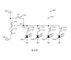
500、800:電路圖500, 800: circuit diagram
502:重設電晶體502: reset transistor
504:電源504: Power
506:源極隨耦器電晶體506: source follower transistor
508:輸出508: output
510:列選擇電晶體510: column selection transistor
900、1000、1100、1200、1300、1400、1500、1600、1700:橫截面視圖900, 1000, 1100, 1200, 1300, 1400, 1500, 1600, 1700: cross-sectional view
1002:溝渠硬罩幕1002: Ditch Hard Screen
1004:溝渠1004: ditch
1102:轉移閘極層1102: transfer gate layer
1402:積體電路晶片1402: Integrated Circuit Chip
1502:罩幕1502: hood
1504:背側溝渠結構1504: Backside trench structure
1800:方塊圖1800: block diagram
1802、1804、1806、1808、1810、1812、1814、1816:動作1802, 1804, 1806, 1808, 1810, 1812, 1814, 1816: action
d1:第一深度d1 : first depth
d2:第二深度d2 : second depth
d3:第三深度d3 : third depth
do:垂直重疊距離do : vertical overlap distance
h1:高度h1 : height
ts:整個厚度ts : the entire thickness
A-A':截面線A-A': Section line
DT:深度DT : Depth
WT:寬度WT : width
結合隨附圖式閱讀以下實施方式時會最佳地理解本揭露內容的態樣。應注意,根據業界中的標準慣例,各種特徵未按比例繪製。事實上,為論述清楚起見,可任意增大或減小各種特徵的尺寸。This disclosure will be best understood when you read the following embodiments in conjunction with the accompanying drawingsThe aspect of the content. It should be noted that, according to standard practices in the industry, various features are not drawn to scale. In fact, for clarity of discussion, the size of various features can be increased or decreased arbitrarily.
圖1A示出絕緣體上半導體(semiconductor-on-insulator)影像感測器的一些實施例的橫截面視圖。FIG. 1A shows a cross-sectional view of some embodiments of a semiconductor-on-insulator image sensor.
圖1B示出圖1A的影像感測器的一些實施例的簡化頂部佈局,其中每一畫素包含具有單一垂直閘極電極部分的轉移電晶體。FIG. 1B shows a simplified top layout of some embodiments of the image sensor of FIG. 1A, in which each pixel includes a transfer transistor with a single vertical gate electrode portion.
圖1C示出圖1A的影像感測器的一些其他實施例的簡化頂部佈局,其中每一畫素包含具有多個垂直閘極電極部分的轉移電晶體。FIG. 1C shows a simplified top layout of some other embodiments of the image sensor of FIG. 1A, in which each pixel includes a transfer transistor with a plurality of vertical gate electrode portions.
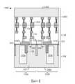
圖2A示出影像感測器的一些更詳細實施例的橫截面視圖。Figure 2A shows a cross-sectional view of some more detailed embodiments of the image sensor.
圖2B示出圖2A的影像感測器的一些實施例的簡化頂部佈局,其中每一畫素包含具有單一垂直閘極電極部分的轉移電晶體。FIG. 2B shows a simplified top layout of some embodiments of the image sensor of FIG. 2A, where each pixel includes a transfer transistor with a single vertical gate electrode portion.
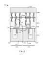
圖3A示出影像感測器的一些更詳細實施例的橫截面視圖。Figure 3A shows a cross-sectional view of some more detailed embodiments of the image sensor.
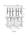
圖3B示出圖3A的影像感測器的一些實施例的簡化頂部佈局。FIG. 3B shows a simplified top layout of some embodiments of the image sensor of FIG. 3A.
圖4A示出包含在零閘極-源極電壓下正常導通(normally ON)的空乏模式垂直轉移閘極電晶體的影像感測器的一些更詳細實施例的橫截面視圖。4A shows a cross-sectional view of some more detailed embodiments of an image sensor including a depletion mode vertical transfer gate transistor that is normally ON at zero gate-source voltage.
圖4B及圖4C示出圖4A的影像感測器的一些實施例的簡化頂部佈局。4B and 4C show simplified top layouts of some embodiments of the image sensor of FIG. 4A.
圖5示出影像感測器的一些實施例的電路圖。Figure 5 shows a circuit diagram of some embodiments of the image sensor.
圖6示出影像感測器的一些更詳細實施例的橫截面視圖。Figure 6 shows a cross-sectional view of some more detailed embodiments of the image sensor.
圖7示出對應於圖6的影像感測器的一些實施例的簡化頂部佈局。FIG. 7 shows a simplified top view of some embodiments of the image sensor corresponding to FIG. 6layout.
圖8提供根據與圖6至圖7一致的一些實施例的影像感測器的電路圖。FIG. 8 provides a circuit diagram of an image sensor according to some embodiments consistent with FIG. 6 to FIG. 7.
圖9至圖17示出用於形成影像感測器的方法的一些實施例的一系列橫截面視圖。Figures 9-17 show a series of cross-sectional views of some embodiments of a method for forming an image sensor.
圖18示出圖9至圖17的方法的一些實施例的方塊圖。Figure 18 shows a block diagram of some embodiments of the methods of Figures 9-17.
本揭露內容提供用於實施本揭露內容的不同特徵的許多不同實施例或實例。下文描述組件及配置的具體實例以簡化本揭露內容。當然,此等具體實例僅為實例且並不意欲為限制性的。舉例而言,在以下描述中,第一特徵在第二特徵上方或第二特徵上形成可包含第一特徵與第二特徵直接接觸地形成的實施例,且亦可包含額外特徵可在第一特徵與第二特徵之間形成以使得第一特徵與第二特徵可能不直接接觸的實施例。此外,本揭露內容可在各種實例中重複附圖標號及/或字母。此重複是出於簡單及清楚的目的,且本身並不規定所論述的各種實施例及/或組態之間的關係。The disclosure provides many different embodiments or examples for implementing different features of the disclosure. Specific examples of components and configurations are described below to simplify the disclosure. Of course, these specific examples are only examples and are not intended to be limiting. For example, in the following description, the formation of the first feature above or on the second feature may include an embodiment in which the first feature is formed in direct contact with the second feature, and may also include additional features that may be formed on the first feature. An embodiment formed between the feature and the second feature such that the first feature and the second feature may not be in direct contact. In addition, the content of the present disclosure may repeat icon numbers and/or letters in various examples. This repetition is for the purpose of simplicity and clarity, and does not itself stipulate the relationship between the various embodiments and/or configurations discussed.
另外,為易於描述,本文中可使用諸如「在......之下(beneath)」、「在......下方(below)」、「下部(lower)」、「在......之上(above)」、「上部(upper)」以及類似者的空間相對術語來描述如圖式中所示出的一個部件或特徵與另一部件或特徵的關係。除圖式中所描繪的定向之外,空間相對術語意欲涵蓋元件在使用或操作中的不同定向。設備可以其他方式定向(旋轉90度或處於其他定向)且本文中所使用的空間相對描述詞可同樣相應地進行解譯。In addition, for ease of description, examples such as "below", "below", "lower", and "below" can be used in this article. ..... The spatial relative terms of "above", "upper" and the like describe the relationship between one component or feature and another component or feature as shown in the diagram. In addition to the orientations depicted in the drawings, spatially relative terms are intended to cover different orientations of elements in use or operation. The device can be oriented in other ways (rotated 90 degrees orHe is directed) and the spatial relative descriptors used in this article can be interpreted accordingly.
CMOS影像感測器用於諸如(例如)相機、平板電腦、智慧型電話等等的各種現代電子元件中。CMOS影像感測器包含以列及行配置於半導體基底上的畫素陣列。當入射光打在畫素上時,光的強度及/或色彩產生各別畫素的各別電訊號,且此等電訊號用來構建數位影像。理想情況下,來自每一畫素的電訊號將精確地僅對應於入射於所述畫素上的光,然而,來自一個畫素的光中的一些可能經由反射或折射「洩漏(leak)」至其他畫素,及/或在一個畫素處產生的電載子可能經由基底「洩漏」至另一畫素。此等及其他問題可能以各種方式體現,且可在一些情境中稱為串擾(cross-talk)、光暈(blooming)等。CMOS image sensors are used in various modern electronic components such as, for example, cameras, tablet computers, smart phones, and so on. The CMOS image sensor includes a pixel array arranged in columns and rows on a semiconductor substrate. When incident light hits a pixel, the intensity and/or color of the light generates individual electrical signals for each pixel, and these electrical signals are used to construct a digital image. Ideally, the electrical signal from each pixel will exactly correspond to the light incident on that pixel. However, some of the light from one pixel may "leak" through reflection or refraction. To other pixels, and/or electric carriers generated at one pixel may "leak" to another pixel through the substrate. These and other problems may manifest in various ways, and may be referred to as cross-talk, blooming, etc. in some contexts.
為限制此等效應,影像感測器包含相鄰畫素之間的背側隔離結構。一些背側隔離結構可自半導體基底的背側延伸穿過基底的整個厚度。儘管此類隔離結構提供良好隔離,然而已瞭解,此類結構使所得影像感測器易遭受開裂(crack)。因此,在本揭露內容的一些態樣中,背側隔離結構在未完全穿過基底延伸(例如,背側隔離結構僅部分地延伸至半導體基底中)的情況下自基底的背側朝向基底的前側延伸。另外,在此等實施例中,畫素的多個電晶體中的一或多者包含閘極電極,閘極電極具有向下延伸至基底的前側中的垂直部分。背側隔離結構具有與閘極電極的垂直部分的垂直重疊部分。此垂直重疊部分提供相鄰畫素之間的相當良好的隔離且降低開裂的風險,使得影像感測器可具有光偵測器之間的較高光學隔離及電隔離且可以高良率來製造。To limit these effects, the image sensor includes a backside isolation structure between adjacent pixels. Some backside isolation structures can extend from the backside of the semiconductor substrate through the entire thickness of the substrate. Although such isolation structures provide good isolation, it is understood that such structures make the resulting image sensor vulnerable to cracks. Therefore, in some aspects of the present disclosure, the backside isolation structure does not extend completely through the substrate (for example, the backside isolation structure only partially extends into the semiconductor substrate) from the backside of the substrate toward the bottom of the substrate. The front side extends. In addition, in these embodiments, one or more of the plurality of transistors of the pixel includes a gate electrode, and the gate electrode has a vertical portion extending down into the front side of the substrate. The backside isolation structure has a vertical overlap portion with the vertical portion of the gate electrode. This vertical overlap portion provides relatively good isolation between adjacent pixels and reduces the risk of cracking, so that the image sensor can have higher optical and electrical isolation between the photodetectors and can be manufactured with high yield.
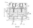
圖1A及圖1B(現在同時參看所述圖1A及所述圖1B)描繪影像感測器100的一些實施例。更特定而言,圖1A示出影像感測器100的橫截面視圖,且圖1B示出影像感測器100的對應頂視圖,如由截面線A-A'所指示。應瞭解,圖1A及圖1B為簡化圖式,且其他未示出特徵通常存在於實際實施方案中。另外,儘管圖1B繪示徑向設置於中心點周圍的四個畫素,但在其他實施例中,可使用其他配置--例如可在中心點周圍配置三個畫素、五個畫素等;或在其他實施例中畫素可不具有中心點。FIG. 1A and FIG. 1B (see also the FIG. 1A and the FIG. 1B at the same time) depict some embodiments of the
影像感測器100包含配置於半導體基底104中或上方的多個畫素。在所示出實例中,畫素102包含以柵格狀方式配置的第一畫素102a、第二畫素102b、第三畫素102c以及第四畫素102d,但總體而言可存在任何數目個畫素。由於多個畫素102通常具有彼此相同的特徵,故以下描述將在理解第一畫素102a的每一所描述特徵適用於其他個別畫素中的每一者的情況下來談論第一畫素102a,而非分別提出每一個別畫素的每一特徵。另外,應瞭解,雖然多個畫素102中的每一者通常具有彼此相同的特徵,但多個畫素(例如,第一畫素102a)中的一或多者可具有可相對於其他畫素(例如,第二畫素102b、第三畫素102c以及第四畫素102d)的佈局而略微旋轉及/或更改的佈局,例如以便將多個畫素102以柵格狀方式「平鋪(tile)」在一起。The
第一畫素102a包含第一光偵測器106a。第一光偵測器106a由光接面(photojunction)定義,其中基底104的第一塊狀區107a與第一集極(collector)區110a接觸。第一塊狀區107a與第一集極區110a具有相反摻雜類型,使得光接面可例如為PN接面或其他合適的光接面。舉例而言,第一塊狀區107a可為p型且第一集極區110a可為n型。第二畫素102b、第三畫素102c以及第四畫素102d分別包含第二光偵測器106b、第三光偵測器106c以及第四光偵測器106d;所述第二光偵測器106b、所述第三光偵測器106c以及所述第四光偵測器106d分別包含第二塊狀區107b、第三塊狀區107c以及第四塊狀區107d;以及第二集極區110b、第三集極區110c以及第四集極區110d。The
第一畫素102a更包含設置於第一光偵測器106a上方的第一轉移電晶體112a。第一轉移電晶體112a包括轉移閘極電極,所述轉移閘極電極包含在半導體基底104的前側104f上方延伸的第一橫向部分114a,及延伸至半導體基底104的前側104f下方的第一深度d1的第一垂直部分116a。第一垂直部分116a突出至第一集極區110a中,但藉由轉移閘極介電層113與第一集極區110a分隔開。轉移閘極介電層113可為或包括例如二氧化矽、高介電常數(k)介電質及/或一些其他合適的介電質。第一浮置節點120a具有與第一集極區110a相同的摻雜類型及與第一塊狀區107a相反的摻雜類型,使得第一通道區121a在第一塊狀區107a中與第一轉移閘極電極的第一垂直部分116a並排地延伸。第一轉移閘極電極可為或包括例如摻雜多晶矽及/或一些其他合適的導電材料,諸如金屬,包括銅、鎢、鋁或其他金屬。所示出實施例亦分別示出第二轉移電晶體112b、第三轉移電晶體112c以及第四轉移電晶體112d;所述第二轉移電晶體112b、所述第三轉移電晶體112c以及所述第四轉移電晶體112d分別具有第二橫向部分114b及第二垂直部分116b;第三橫向部分114c及第三垂直部分116c;以及第四橫向部分114d及第四垂直部分116d。The
背側溝渠隔離結構122自半導體基底104的背側104b延伸至半導體基底104的前側104f下方的第二深度d2,且橫向地包圍個別畫素的個別塊狀區以將多個光偵測器彼此電隔離且光學隔離。因此,背側溝渠隔離結構122自基底104的背側104b部分地朝向基底104的前側104f延伸,但不穿過基底104的整個厚度ts。背側溝渠隔離結構122可例如為或包括二氧化矽及/或一些其他合適的介電質。背側溝渠隔離結構包含若干環形結構,其中每一環形結構橫向地包圍對應畫素的塊狀區,且多個環形結構彼此拼接以提供柵格狀幾何形狀給背側溝渠隔離結構。The backside
第二深度d2小於第一深度d1,使得第一轉移電晶體電極的第一垂直部分116a的最下部部分與背側溝渠隔離結構122的最上部部分具有垂直重疊距離do。在一些實施例中,第一深度d1與第二深度d2的比例在大約1.05至2.0範圍內,及/或垂直重疊距離do在第一深度d1的5%至50%範圍內,及/或垂直重疊距離do在第二深度d2的5%至50%範圍內。在一些實施例中,第一深度d1在525奈米至1200奈米範圍內(且在一些實施例中為大約600奈米),第二深度d2在500奈米至1000奈米範圍內(且在一些實施例中為大約500奈米),且垂直重疊距離do在25奈米至700奈米範圍內(且在一些實施例中為大約100奈米)。另外,在一些實施例中,背側溝渠隔離結構122的高度h1在基底104的整個厚度ts的大約25%至基底104的整個厚度ts的大約95%範圍內,且在一些實施例中,垂直重疊距離do可在h1的大約5%至h1的大約50%範圍內。The second depth d2 is smaller than the first depth d1 , so that the lowermost portion of the first
內連線結構124設置於基底104的前側104f上方。內連線結構124包含堆疊於轉移電晶體上方的多個電線126、多個接點128以及多個通孔130。電線126及/或通孔130可為或包括相同材料、鋁銅、鋁、銅、一些其他合適的導電材料,或前述的任何組合。接點128可為或包括例如鎢、銅、鋁銅、一些其他合適的導電材料,或前述的任何組合。金屬間介電層132包圍電線126、接點128、通孔130以及基底104的前側上的其他結構。金屬間介電層132可為或包括例如二氧化矽、低k介電質、碳化矽、氮化矽、一些其他合適的介電質,或前述的任何組合。The
在一些實施例中,舉例而言,多個畫素102被配置為偵測不同波長的入射光,諸如紅光、綠光以及藍光。為有助於此偵測,畫素包含濾色器134(例如,第一畫素102a上方的第一濾色器134a、第二畫素102b上方的第二濾色器134b)及各別微透鏡136(第一畫素102a上方的第一微透鏡136a、第二畫素102b上方的第二微透鏡136b)。各種濾色器134例如根據拜耳濾波器(Bayer-filter)圖案來對不同波長的光進行濾波,使得多個畫素102偵測不同波長的光。因此,例如在操作期間,入射光138打在第一微透鏡136a上、經導引穿過對入射光138進行濾波的第一濾色器134a,且接著經濾波的光朝向第一畫素102a的第一光偵測器106a行進。經濾波的光接著與第一光偵測器106a相互作用以變換成電訊號,所述電訊號藉由畫素的電路(包含第一轉移電晶體112a及內連線結構124)來處理。因此,多個畫素102可經由此等電訊號共同產生數位影像資料。In some embodiments, for example, the plurality of
由於背側溝渠隔離結構122具有與第一轉移閘極電極的第一垂直部分116a的垂直重疊(垂直重疊距離do),故影像感測器100可具有第一光偵測器106a、第二光偵測器106b、第三光偵測器106c以及第四光偵測器106d之間的高光學隔離及高電隔離。高光學隔離可得到第一光偵測器106a、第二光偵測器106b、第三光偵測器106c以及第四光偵測器106d之間的低串擾及高調變轉移函數(modulation transfer function)。高電隔離可得到高滿井容量(full well capacity)且因此可得到高抗光暈,同時亦高效地製造。另外,儘管背側溝渠隔離結構122可原則上整個穿過基底104,但限制背側溝渠隔離結構的範圍限制了基底104開裂的風險,使得所示出的實施方案可提供比一些其他途徑更高的良率。Since the backside
儘管圖1B示出其中每一畫素包含具有單一垂直閘極電極部分的轉移電晶體的實例,但轉移電晶體亦可包含多個垂直閘極電極部分。因此,圖1C示出其中每一畫素包含具有兩個垂直閘極電極部分的轉移電晶體的另一實例。舉例而言,第一畫素包含第一轉移電晶體,所述第一轉移電晶體包含具有兩個第一垂直部分116a的閘極電極,所述兩個第一垂直部分116a在第一閘極電極的第一橫向部分114a下方間隔開。額外垂直閘極電極部分的存在可有助於使得電荷能夠更快地自光偵測器轉移至浮置節點。然而,如先前在圖1B中所示出的具有單一垂直閘極電極部分的實施例可在一些情況下提供具有更小佔據面積的畫素。Although FIG. 1B shows an example in which each pixel includes a transfer transistor having a single vertical gate electrode portion, the transfer transistor may also include a plurality of vertical gate electrode portions. Therefore, FIG. 1C shows another example in which each pixel includes a transfer transistor having two vertical gate electrode portions. For example, the first pixel includes a first transfer transistor, the first transfer transistor includes a gate electrode having two first
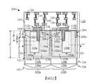
參看圖2A,提供影像感測器200的一些更詳細實施例的橫截面視圖。圖2B提供與圖2A一致的頂視圖的實例。影像感測器200可包括圖1A至圖1C中的影像感測器100的一些態樣(且反之亦然);且因此,上文關於圖1A至圖1C所解釋的特徵亦適用於圖2A至圖2B中的影像感測器200。2A, a cross-sectional view of some more detailed embodiments of the
如圖2A至圖2B中所示出,在一些實施例中,背側溝渠隔離結構122可具有成角度(angled)及/或漸縮(tapered)側壁122as,而非具有垂直側壁122vs的背側溝渠隔離結構122(亦參見圖1A),所述成角度及/或漸縮側壁122as愈靠近基底的前側104f則愈窄且愈靠近基底的背側104b則愈寬。另外,第一轉移閘極電極的第一垂直部分116a亦可為成角度的或漸縮的,使得第一垂直部分116a的最底部部分具有較窄側壁,而第一垂直部分116a的上部部分具有較寬側壁。另外,在一些實施例中,背側溝渠隔離結構122可具有水平部分122h,而第一塊狀區107a並非直接接觸第一濾色器134a(如先前在圖1A中所示出),所述水平部分122h覆蓋基底的背側104b以將基底104的第一塊狀區107a與第一濾色器134a分隔開。因此,在圖2A中,背側溝渠隔離結構122包括建立柵格狀結構以將多個畫素102彼此分隔開的多個垂直區段122v,以及覆蓋基底的背側104b的水平部分122h。As shown in FIGS. 2A to 2B, in some embodiments, the backside
除上文關於圖1A至圖1C所解釋的特徵之外,圖2A至圖2B的影像感測器200更包括摻雜區202,所述摻雜區202包含自基底的前側104f延伸至第三深度d3的多個垂直區段202v。摻雜區202設置於背側溝渠隔離結構122上方且橫向地包圍塊狀區107以形成類似於背側溝渠隔離結構122的柵格狀結構,藉此有助於進一步將畫素的第一光偵測器106a、第二光偵測器106b、第三光偵測器106c以及第四光偵測器106d彼此隔離。在一些實施例中,第三深度d3等於第二深度d2,因此摻雜區與背側溝渠隔離結構122的垂直區段122v的最上部部分接觸。因此,在一些實施例中,摻雜區202及背側溝渠隔離結構122共同跨越基底104的整個厚度ts。摻雜區202具有與塊狀區107相同且與浮置節點120及集極區110相反的摻雜類型。舉例而言,在一些實施例中,浮置節點120及集極區110可各自為n型半導體材料,且塊狀區107及摻雜區202為p型半導體材料。在一些實施例中,摻雜區202可具有大於塊狀區107的摻雜濃度--例如,摻雜區202可具有在1e16每立方公分至1e18每立方公分範圍內的第一摻雜濃度,且塊狀區107可具有在1e16每立方公分至1e18每立方公分範圍內的第二摻雜濃度。In addition to the features explained above with respect to FIGS. 1A to 1C, the
在一些實施例中,背側溝渠隔離結構122的多個垂直區段122v各自具有第一寬度,且摻雜區202的垂直區段202v各自具有與第一寬度相等的第二寬度,但第二寬度亦可小於或大於第一寬度。另外,歸因於摻雜區202及背側溝渠隔離結構122所形成的方式,摻雜區202可延伸,因此柵格狀結構的多個垂直區段202v具有對應於第一軸線或平面202a的中心軸線,且背側溝渠隔離結構122可延伸,因此柵格狀結構的垂直區段122v具有對應於第二軸線或平面122a的中心軸線,所述第二軸線或平面122a自第一軸線或平面202a略微偏移。此偏移可產生於在用以製造此等結構的微影製程期間出現的較小未對準,從而導致背側溝渠隔離結構122的側壁及/或中心軸線與摻雜區202的側壁及/或中心軸線未對準/偏移。另外,歸因於摻雜區202及背側溝渠隔離結構122所形成的方式,摻雜區202可具有向下延伸超過背側溝渠隔離結構122的最上部表面的最底部表面,使得第三深度d3略微大於第二深度d2,從而在摻雜區202的下部部分中產生階梯狀特徵204。In some embodiments, the
同樣,背側溝渠隔離結構122與轉移閘極電極的垂直部分116之間的垂直重疊(垂直重疊距離do)提供了具有光偵測器106之間的高光學隔離及高電隔離的影像感測器200。高光學隔離可得到第一光偵測器106a、第二光偵測器106b、第三光偵測器106c以及第四光偵測器106d之間的低串擾及高調變轉移函數。高電隔離可得到高滿井容量且因此可得到高抗光暈,同時亦高效地製造。Similarly, the vertical overlap (the vertical overlap distance do) between the
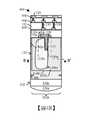
參看圖3A,提供影像感測器300的一些更詳細實施例的橫截面視圖,而圖3B提供與圖3A一致的頂視圖。影像感測器300可包括圖1A至圖1C中的影像感測器100的一些態樣(且反之亦然),及/或圖2A至圖2B中的影像感測器200的一些態樣(且反之亦然);且因此,上文關於圖1A至圖1C及/或圖2A至圖2B所解釋的特徵亦適用於圖3A至圖3B中的影像感測器300。Referring to FIG. 3A, a cross-sectional view of some more detailed embodiments of the
除先前所論述的特徵之外,圖3A至圖3B中的轉移電晶體亦包含設置於轉移閘極電極的側壁上的側壁間隔件312。側壁間隔件312可為或包括例如二氧化矽、氮化矽、一些其他合適的介電質,或前述的任何組合。In addition to the previously discussed features, the transfer transistor in FIGS. 3A to 3B also includes
另外,影像感測器300的背側溝渠隔離結構122由背側介電質襯裡302及背側介電層304定義。背側介電質襯裡302鑲襯基底104的背側且將背側溝渠隔離結構的背側介電層304與基底104的塊狀區107分隔開。背側介電質襯裡302可例如為或包括高k介電層及/或一些其他合適的介電質。背側介電層304可例如為或包括二氧化矽及/或一些其他合適的介電質。背側介電層304覆蓋基底104的背側上的背側介電質襯裡302且容納屏蔽件306。In addition, the backside
屏蔽件306防止自基底104的背側接收到的輻射照射於背側溝渠隔離結構122上。另外,屏蔽件306的側壁將自基底104的背側接收到的輻射朝向第一光偵測器106a、第二光偵測器106b、第三光偵測器106c以及第四光偵測器106d反射以減小串擾且增強影像感測器的量子效率。屏蔽件306包含多個區段,所述屏蔽件306的多個區段獨立於背側溝渠隔離結構122的多個區段且分別位於背側溝渠隔離結構122的多個區段之下。屏蔽件306可例如為或包括金屬及/或一些其他合適的反射性材料。The shielding
內連線結構124包含設置於金屬間介電(inter-metal dielectric;IMD)層132內的多個電線126、多個接點128、多個通孔130,所述IMD層132堆疊於基底104的前側上且藉由多個蝕刻終止層308彼此分隔開。IMD層132及蝕刻終止層308共同定義基底104的前側上的前側介電層。IMD層132可為或包括例如二氧化矽、低k介電質、一些其他合適的介電質,或前述的任何組合。蝕刻終止層308可為或包括例如氮化矽、碳化矽、一些其他合適的蝕刻終止材料,或前述的任何組合。The
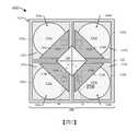
參看圖4A,提供影像感測器400的一些更詳細實施例的橫截面視圖,而圖4B提供與圖4A一致的頂視圖。影像感測器400可包括圖1A至圖1C中的影像感測器100的一些態樣(且反之亦然),及/或圖2A至圖2B中的影像感測器200的一些態樣(且反之亦然),及/或圖3A至圖3B中的影像感測器300的一些態樣(且反之亦然);且因此,上文關於圖1A至圖1C及/或圖2A至圖2B及/或圖3A至圖3B所解釋的特徵亦適用於圖4A至圖4B中的影像感測器400。Referring to FIG. 4A, a cross-sectional view of some more detailed embodiments of the
圖4A至圖4C共同描繪其中垂直轉移電晶體為空乏模式(depletion mode)電晶體的實例。因此,如圖4C中所繪示,在閘極電極的一些部分下方,集極區110a可為n型且可在第一浮置節點120a與第一集極110a之間持續延伸。因此,在不存在正閘極-源極電壓的情況下,轉移電晶體為「導通」(導電)的,且為了使電晶體截止,施加閘極-源極電壓以使來自閘極電極下方的集極區110a的載子空乏,藉此夾止(pinch off)電晶體且將第一浮置節點120a與第一集極區110a隔離。4A to 4C collectively depict an example in which the vertical transfer transistor is a depletion mode transistor. Therefore, as shown in FIG. 4C, under some parts of the gate electrode, the
參看圖5,提供包含圖1A至圖1B的影像感測器的一些實施例的電路圖500。Referring to FIG. 5, a circuit diagram 500 including some embodiments of the image sensor of FIGS. 1A to 1B is provided.
如所繪示,圖5的影像感測器包含一或多個畫素102,所述一或多個畫素102具有藉助於轉移電晶體112而電性連接的一或多個對應的光偵測器106。光偵測器106累積來自入射於光偵測器106上的光子的電荷(例如,電子)。轉移電晶體112選擇性地將電荷自光偵測器106轉移至影像感測器。重設電晶體502電連接於電源504與浮置節點之間以選擇性地清除浮置節點處的電荷。源極隨耦器(source follower)電晶體506電連接於電源504與輸出508之間,且藉由浮置節點120閘控,以允許在不移除電荷的情況下觀測到浮置節點120處的電荷。列選擇電晶體510電連接於源極隨耦器電晶體506與輸出508之間以選擇性地輸出與浮置節點120處的電壓成比例的電壓。As shown, the image sensor of FIG. 5 includes one or
在圖5的影像感測器的使用期間,畫素102經暴露於光學影像持續預定積分時段。在此時間段內,畫素102藉由累積與光偵測器106的集極區(未繪示)中的光強度成比例的電荷來記錄入射於光偵測器106上的光的強度。在預定積分時段之後,針對光偵測器106中的每一者讀取所累積電荷的量。在一些實施例中,藉由瞬時激活重設電晶體502以清除儲存於浮置節點120處的電荷來讀取光偵測器106的所累積電荷的量。此後,激活列選擇電晶體510,且藉由激活轉移電晶體112持續預定轉移時段來將光偵測器106的所累積電荷轉移至浮置節點120。在預定轉移時段期間,監測輸出508處的電壓。在預定轉移時段之後,在輸出508處觀測到的電壓的改變與在光偵測器106處所記錄的光的強度成比例。During the use of the image sensor of FIG. 5, the
圖6及圖7(現在同時參看所述圖6及所述圖7)描繪影像感測器600的一些實施例。更特定而言,圖6示出影像感測器600的橫截面視圖,且圖7示出影像感測器600的對應頂視圖,如由截面線A-A'所指示。圖6及圖7類似於圖1A至圖1B,不同之處在於圖1A至圖1B示出其中每一畫素具有單獨浮置擴散節點的情況,而圖6至圖7示出其中單一浮置節點120被多個畫素中的每一者共用的情況。在圖6至圖7中,單一浮置擴散節點120具有下部表面,所述下部表面與位於單一浮置節點120正下方的垂直區段302v的最上部表面形成接面。Figures 6 and 7 (referring to both the Figure 6 and Figure 7 now) depict some embodiments of the
圖8提供根據與圖6至圖7一致的一些實施例的影像感測器600的電路圖800。如所繪示,影像感測器600包含一或多個光偵測器(光偵測器106a至光偵測器106d),所述一或多個光偵測器分別藉助於對應轉移電晶體(轉移電晶體112a至轉移電晶體112d)而電性連接至浮置節點120。光偵測器106a至光偵測器106d累積來自入射於光偵測器106a至光偵測器106d上的光子的電荷(例如,電子)。轉移電晶體112a至轉移電晶體112d分別選擇性地將電荷自光偵測器106a至光偵測器106d轉移至浮置節點120。重設電晶體502電連接於電源504與浮置節點120之間以選擇性地清除浮置節點120處的電荷。源極隨耦器電晶體506電連接於電源504與輸出508之間,且藉由浮置節點120閘控,以允許在不移除電荷的情況下觀測到浮置節點120處的電荷。列選擇電晶體510電連接於源極隨耦器電晶體506與輸出508之間以選擇性地輸出與浮置節點120處的電壓成比例的電壓。FIG. 8 provides a circuit diagram 800 of the
在影像感測器600的使用期間,影像感測器600經暴露於光學影像持續預定積分時段。在此時間段內,影像感測器600藉由累積與光偵測器106a至光偵測器106d的集極區(未繪示)中的光強度成比例的電荷來記錄入射於光偵測器106a至光偵測器106d上的光的強度。在預定積分時段之後,針對光偵測器106a至光偵測器106d中的每一者讀取所累積電荷的量。在一些實施例中,藉由瞬時激活重設電晶體502以清除儲存於浮置節點120處的電荷來讀取光偵測器的所累積電荷的量。此後,激活列選擇電晶體510,且藉由激活對應光偵測器(例如,第一光偵測器106a)的轉移電晶體(例如,第一轉移電晶體112a)持續預定轉移時段來將光偵測器(例如,第一光偵測器106a)的所累積電荷轉移至浮置節點120。在預定轉移時段期間,監測輸出508處的電壓。隨著電荷轉移,輸出508處的電壓改變。在預定轉移時段之後,在輸出508處觀測到的電壓的改變與在光偵測器處所記錄的光的強度成比例。接著可類似地量測入射於其他光偵測器(例如,光偵測器106b至光偵測器106d)上的光。During the use of the
參看圖9至圖17,提供用於形成影像感測器的方法的一些實施例的一系列橫截面視圖900至橫截面視圖1700。9-17, a series of
如藉由圖9的橫截面視圖900所示出,在基底104中進行一系列選擇性摻雜製程以形成集極區110a、集極區110b以及摻雜區202。基底104包含前側104f及背側104b,且可例如為塊狀單晶矽基底、絕緣體上半導體(semiconductor or insulator;SOI)基底,或一些其他合適的半導體基底。As shown by the
集極區110a、集極區110b獨立於畫素,且共用共同摻雜類型,所述共同摻雜類型與塊狀區107及摻雜區202的摻雜類型相反。舉例而言,塊狀區107及摻雜區202可具有p型摻雜,且集極區110a、集極區110b可具有n型摻雜。舉例而言,摻雜區202可具有在1e16每立方公分至1e18每立方公分範圍內的摻雜濃度,塊狀區107可具有在1e16每立方公分至1e18每立方公分範圍內的摻雜濃度,且集極區110a、集極區110b可具有在1e16每立方公分至1e18每立方公分範圍內的摻雜濃度。The
在一些實施例中,選擇性摻雜製程藉由選擇性離子植入或一些其他合適的選擇性摻雜製程來進行。舉例而言,可進行第一選擇性離子植入以形成集極區110a、集極區110b,且可隨後進行第二選擇性離子植入以形成摻雜區202。選擇性離子植入可例如包括藉由微影形成光阻罩幕、利用適當位置上的光阻罩幕在基底104中進行離子植入,以及移除光阻罩幕。In some embodiments, the selective doping process is performed by selective ion implantation or some other suitable selective doping process. For example, a first selective ion implantation may be performed to form the
如藉由圖10的橫截面視圖1000所示出,溝渠硬罩幕1002形成於半導體基底104的前側104f上。溝渠硬罩幕1002具有所形成的轉移閘極電極的溝渠的佈局。溝渠硬罩幕1002可例如藉由沈積硬罩幕層且隨後使所述硬罩幕層圖案化成溝渠硬罩幕1002來形成。溝渠硬罩幕1002可為或包括例如氮化矽及/或一些其他合適的硬罩幕材料。As shown by the
亦藉由圖10的橫截面視圖1000所示出,在半導體基底104的前側104f中進行蝕刻。利用就位的溝渠硬罩幕1002進行蝕刻,且形成獨立於畫素102且分別位於畫素102處的多個溝渠1004。在一些實施例中,第一蝕刻形成具有約250奈米(nm)至450奈米、約250奈米至350奈米、約350奈米至450奈米或一些其他合適的值的深度DT的溝渠1004。另外,在一些實施例中,第一蝕刻形成具有約80奈米至150奈米、約80奈米至105奈米、約105奈米至150奈米或一些其他合適的值的寬度WT的溝渠1004。As also shown by the
如藉由圖11的橫截面視圖1100所示出,轉移閘極介電層113形成於基底104上。轉移閘極介電層113可為或包括例如二氧化矽及/或一些其他合適的介電質。另外,轉移閘極介電層113可例如藉由臨場蒸汽產生(in situ steam generation;ISSG)、氣相沈積或一些其他合適的生長及/或沈積製程來形成。As shown by the
亦藉由圖11的橫截面視圖1100所示出,轉移閘極層1102形成於轉移閘極介電層113上方。轉移閘極層1102可例如為或包括摻雜多晶矽及/或一些其他合適的導電材料。轉移閘極層1102可例如藉由氣相沈積及/或一些其他合適的沈積製程來形成。As also shown by the
如藉由圖12的橫截面視圖1200所示出,使轉移閘極層1102(參見圖11)圖案化以形成獨立於畫素102a、畫素102b且分別位於畫素102a、畫素102b處的多個轉移閘極電極。轉移閘極電極可例如具有如圖1B及/或圖2B及/或圖3B及/或圖4A中所繪示的頂部佈局。在一些實施例中,用於使轉移閘極層1102圖案化的製程包括:1)沈積抗反射塗層(antireflective coating;ARC);2)藉由微影/蝕刻製程使ARC及轉移閘極層1102圖案化;以及3)移除ARC。然而,其他製程亦可適用。As shown by the
亦藉由圖12的橫截面視圖1200所示出,多個浮置節點120形成於塊狀區107中。多個浮置節點120可獨立於畫素102a、畫素102b且分別位於畫素102a、畫素102b處。浮置節點120可例如具有如圖1B及/或圖2B及/或圖3B及/或圖4A中所繪示的頂部佈局。浮置節點120可例如藉由選擇性離子植入及/或一些其他合適的選擇性摻雜製程來形成。選擇性離子植入可例如包括藉由微影形成光阻罩幕、利用就位的光阻罩幕進行離子植入,以及移除光阻罩幕。As also shown by the
如藉由圖13的橫截面視圖1300所示出,金屬間介電層132形成於轉移閘極電極上方。金屬間介電層132可例如為或包括二氧化矽、低k介電質及/或一些其他合適的介電質。在一些實施例中,用於形成金屬間介電層132的製程包括:1)沈積金屬間介電層132;以及2)在金屬間介電層132的頂部表面中進行平坦化。如藉由圖13的橫截面視圖1300所進一步示出,內連線結構124形成於金屬間介電層132中及/或金屬間介電層132上方。內連線結構124包括多個電線126、多個接點128以及多個通孔130。As shown by the
如藉由圖14的橫截面視圖1400所示出,將圖13的結構垂直地翻轉且接合至積體電路(integrated circuit;IC)晶片1402。所述接合可例如為或包括混合接合或一些其他合適的接合。IC晶片1402僅經部分地繪示,但包括半導體基底1406以及沿著頂部表面的多個電線1404。IC晶片1402的電線1404與內連線結構124的電線126相配,且提供內連線結構124與IC晶片1402之間的電耦接。As shown by the
如藉由圖15的橫截面視圖1500所示出,罩幕1502形成於基底的背側上,且利用就位的罩幕進行蝕刻以形成背側溝渠結構1504。在一些實施例中,蝕刻為提供具有實質上垂直側壁的背側溝渠結構的乾式蝕刻,而在其他實施例中,蝕刻具有賦予側壁漸縮輪廓(例如,接近基底的背側更寬,且愈靠近基底的前側愈窄)的水平分量。As shown by the
如藉由圖16的橫截面視圖1600所示出,形成介電質以填充背側溝渠結構1504,藉此形成背側溝渠隔離結構122。在一些實施例中,例如經由化學氣相沈積(chemical vapor deposition;CVD)製程、電漿氣相沈積製程(plasma vapor deposition process;PVD)或旋塗製程來形成介電質。介電質與摻雜區202接觸以提供相鄰畫素之間的電隔離及光學隔離。當形成時,介電質的最上部部分具有與閘極電極的垂直部分的最下部部分的垂直重疊部分。此配置有助於限制在基底104中形成不合需求的開裂的風險,且提供相鄰畫素之間的良好電隔離及光學隔離。As shown by the
如藉由圖17的橫截面視圖1700所示出,濾色器134a、濾色器134b以及微透鏡136a、微透鏡136b接著形成於基底的背側上。As shown by the
儘管參看一方法來描述圖9至圖17,但應瞭解,圖9至圖17中所繪示的結構不限於所述方法,而是可與所述方法獨立分開。另外,儘管圖9至圖17經描述為一系列動作,但應瞭解,此等動作並非限制性的,而在其他實施例中,可改變動作的次序,且所揭露的方法亦適用於其他結構。在一些實施例中,可整個或部分地省略所示出及/或描述的一些動作。Although FIGS. 9 to 17 are described with reference to a method, it should be understood that the structure shown in FIGS. 9 to 17 is not limited to the method, but can be separated from the method independently.open. In addition, although FIGS. 9-17 are described as a series of actions, it should be understood that these actions are not limitative, and in other embodiments, the sequence of actions can be changed, and the disclosed method is also applicable to other structures . In some embodiments, some actions shown and/or described may be omitted in whole or in part.
參看圖18,提供圖9至圖17的方法的一些實施例的方塊圖1800。Referring to Figure 18, a block diagram 1800 of some embodiments of the methods of Figures 9-17 is provided.
在動作1802處,形成對應於半導體基底中的畫素的光偵測器,且形成橫向地包圍光偵測器及將相鄰光偵測器彼此分隔開的摻雜區。參見例如圖9。At
在動作1804處,在基底的前側中形成溝渠。所述溝渠延伸至光偵測器中。參見例如圖10。At
在動作1806處,形成閘極介電質及閘極電極材料以填充溝渠。使閘極電極材料圖案化以在對應畫素上方形成轉移閘極電極。參見例如圖11至圖12。At action 1806, a gate dielectric and gate electrode material are formed to fill the trench. The gate electrode material is patterned to form a transfer gate electrode above the corresponding pixel. See, for example, Figures 11-12.
在動作1808處,內連線結構形成於半導體基底的前側上方。參見例如圖13。At
在動作1810處,將積體晶片接合至內連線結構的上部表面。參見例如圖14。At
在動作1812處,形成延伸至半導體基底的背側中的背側溝渠結構。背側溝渠結構實質上對準至摻雜區且接觸所述摻雜區,且不完全延伸穿過基底。參見例如圖15。At
在動作1814處,背側溝渠結構填充有介電質以形成背側溝渠隔離結構。背側溝渠隔離結構的最上部部分具有與摻雜區的最下部部分的垂直重疊部分。參見例如圖16。At
在動作1816處,濾色器及微透鏡形成於半導體基底的背側上。參見例如圖17。At
儘管在本文中將圖18的方塊圖1800示出及描述為一系列動作或事件,但應瞭解,不應以限制性意義來解譯此類動作或事件的所示出排序。舉例而言,除本文中所示出及/或描述的動作或事件之外,一些動作可與其他動作或事件以不同次序及/或同時發生。另外,並非可要求所有所示出的動作以實施本文中描述的一或多個態樣或實施例,且本文中所描繪的動作中的一或多者可在一或多個單獨動作及/或階段中進行。Although the block diagram 1800 of FIG. 18 is shown and described herein as a series of actions or events, it should be understood that the illustrated ordering of such actions or events should not be interpreted in a restrictive sense. For example, in addition to the actions or events shown and/or described herein, some actions may occur in a different order and/or simultaneously with other actions or events. In addition, not all of the actions shown may be required to implement one or more aspects or embodiments described herein, and one or more of the actions described herein may be one or more separate actions and/ Or in the stage.
在一些實施例中,本申請案是關於一種影像感測器元件。光偵測器設置於半導體基底中,且轉移電晶體設置於光偵測器上方。所述轉移電晶體包含具有橫向部分及垂直部分的轉移閘極,所述橫向部分在所述半導體基底的前側上方延伸,所述垂直部分延伸至所述半導體基底的所述前側下方的第一深度。閘極介電質將所述橫向部分及所述垂直部分與所述半導體基底分隔開。背側溝渠隔離結構自所述半導體基底的背側延伸至所述半導體基底的所述前側下方的第二深度。所述背側溝渠隔離結構橫向地包圍所述光偵測器,且所述第二深度小於所述第一深度,使得所述轉移電晶體的所述垂直部分的最下部部分具有與所述背側溝渠隔離結構的最上部部分的垂直重疊部分。在實施例中,所述第一深度與所述第二深度的比例在大約1.05至2範圍內。在實施例中,所述第一深度在525奈米與1200奈米之間,且所述第二深度在500奈米與1000奈米之間。在實施例中,半導體元件更包括摻雜區,自所述半導體基底的所述前側延伸至所述第二深度以接觸所述背側溝渠隔離結構的所述最上部部分。在實施例中,所述背側溝渠隔離結構包含垂直隔離區段,所述垂直隔離區段沿所述垂直隔離區段的中心軸具有第一寬度,且所述摻雜區具有垂直摻雜區段,所述垂直摻雜區段沿所述垂直摻雜區段的中心軸具有第二寬度,其中所述垂直隔離區段的所述中心軸自所述垂直摻雜區段的所述中心軸偏移。在實施例中,所述摻雜區具有最底部表面,所述最底部表面向下延伸至所述半導體基底的所述前側下方的第三深度,所述摻雜區延伸超過所述背側溝渠隔離結構的最上部表面,使得所述第三深度略微大於所述第二深度,從而在所述摻雜區的下部部分中產生階梯狀特徵。在實施例中,所述背側溝渠隔離結構包含介電材料的環形結構,所述介電材料的所述環形結構直接接觸所述半導體基底。在實施例中,所述轉移閘極包含兩個垂直部分,所述兩個垂直部分自所述橫向部分延伸至所述半導體基底的所述前側下方的所述第一深度,其中所述兩個垂直部分由所述介電材料的所述環形結構橫向地包圍且彼此橫向地間隔開。在實施例中,所述背側溝渠隔離結構包含介電材料的環形結構,所述元件更包括襯裡,將所述介電材料的所述環形結構與所述半導體基底分隔開。在實施例中,半導體元件更包括摻雜區,所述摻雜區自所述半導體基底的所述前側延伸至所述第二深度以接觸所述襯裡的最上部部分。在實施例中,所述襯裡具有第一寬度,且所述摻雜區具有與所述第一寬度相等的第二寬度。在實施例中,所述背側溝渠隔離結構包含垂直隔離區段,所述垂直隔離區段沿所述垂直隔離區段的中心軸具有第一寬度,且所述摻雜區具有垂直摻雜區段,所述垂直摻雜區段沿所述垂直摻雜區段的中心軸具有第二寬度,其中所述垂直隔離區段的所述中心軸自所述垂直摻雜區段的所述中心軸偏移。In some embodiments, this application relates to an image sensor device. The light detector is arranged in the semiconductor substrate, and the transfer transistor is arranged above the light detector. The transfer transistor includes a transfer gate having a lateral portion and a vertical portion, the lateral portion extending above the front side of the semiconductor substrate, and the vertical portion extending to a first depth below the front side of the semiconductor substrate . The gate dielectric separates the lateral portion and the vertical portion from the semiconductor substrate. The backside trench isolation structure extends from the backside of the semiconductor substrate to a second depth below the front side of the semiconductor substrate. The back-side trench isolation structure laterally surrounds the photodetector, and the second depth is smaller than the first depth, so that the lowermost part of the vertical portion of the transfer transistor has a contact with the back The vertical overlap of the uppermost part of the side trench isolation structure. In an embodiment, the ratio of the first depth to the second depth is in the range of about 1.05 to 2. In an embodiment, the first depth is between 525 nanometers and 1200 nanometers, and the second depth is between 500 nanometers and 1000 nanometers. In an embodiment, the semiconductor element further includes a doped region extending from the front side of the semiconductor substrate to the second depth to contact the backThe uppermost part of the side trench isolation structure. In an embodiment, the backside trench isolation structure includes a vertical isolation section, the vertical isolation section has a first width along a central axis of the vertical isolation section, and the doped region has a vertical doped region Section, the vertical doping section has a second width along the central axis of the vertical doping section, wherein the central axis of the vertical isolation section is from the central axis of the vertical doping section Offset. In an embodiment, the doped region has a bottommost surface, the bottommost surface extends downward to a third depth below the front side of the semiconductor substrate, and the doped region extends beyond the backside trench Isolate the uppermost surface of the structure so that the third depth is slightly larger than the second depth, thereby generating stepped features in the lower portion of the doped region. In an embodiment, the backside trench isolation structure includes a ring structure of a dielectric material, and the ring structure of the dielectric material directly contacts the semiconductor substrate. In an embodiment, the transfer gate includes two vertical portions extending from the lateral portion to the first depth below the front side of the semiconductor substrate, wherein the two The vertical portions are laterally surrounded by the ring structure of the dielectric material and are laterally spaced apart from each other. In an embodiment, the backside trench isolation structure includes a ring structure of a dielectric material, and the device further includes a liner to separate the ring structure of the dielectric material from the semiconductor substrate. In an embodiment, the semiconductor device further includes a doped region that extends from the front side of the semiconductor substrate to the second depth to contact the uppermost part of the liner. In an embodiment, the liner has a first width, and the doped region has a second width equal to the first width. In an embodiment, the backside trench isolation structure includes a vertical isolation section, the vertical isolation section has a first width along a central axis of the vertical isolation section, and the doped region has a vertical doped region Section, the vertical doped section has along the central axis of the vertical doped sectionA second width, wherein the central axis of the vertical isolation section is offset from the central axis of the vertical doping section.
在一些實施例中,本申請案提供一種方法。在所述方法中,分別對應於多個畫素的多個光偵測器形成於半導體基底中。形成橫向地包圍且將相鄰光偵測器彼此分隔開的摻雜區。轉移閘極電極形成於對應畫素上方,其中轉移閘極電極包含橫向部分及垂直部分,所述橫向部分在所述半導體基底的前側上方延伸,所述垂直部分延伸至所述半導體基底的所述前側下方的第一深度。形成延伸至所述半導體基底的背側中的背側溝渠結構,所述背側溝渠結構實質上對準至所述摻雜區且接觸所述摻雜區,且小於整個延伸穿過所述半導體基底。所述背側溝渠結構填充有介電質以形成背側溝渠隔離結構,所述背側溝渠隔離結構的最上部部分具有與所述轉移閘極電極的所述垂直部分的最下部部分的垂直重疊部分。在實施例中,形成所述多個轉移閘極電極包括:形成進入所述半導體基底的前側的多個溝渠,所述多個溝渠延伸至所述多個光偵測器中;形成鑲襯所述多個溝渠的閘極介電質;在所述閘極介電質上方形成閘極電極材料以填充所述多個溝渠;以及使所述閘極電極材料圖案化以形成所述多個轉移閘極電極。在實施例中,方法更包括:在所述半導體基底的所述前側上方及所述多個轉移閘極電極上方形成內連線結構。在實施例中,方法更包括:在所述形成所述背側溝渠結構之前將積體晶片接合至所述內連線結構的上部表面。在實施例中,方法更包括:在形成所述背側溝渠隔離結構之後,在所述半導體基底的所述背側上形成濾色器;在所述半導體基底的所述背側的對面形成微透鏡在所述濾色器上。In some embodiments, this application provides a method. In the method, a plurality of photodetectors respectively corresponding to a plurality of pixels are formed in a semiconductor substrate. A doped region is formed that laterally surrounds and separates adjacent photodetectors from each other. The transfer gate electrode is formed above the corresponding pixel, wherein the transfer gate electrode includes a lateral portion and a vertical portion, the lateral portion extends above the front side of the semiconductor substrate, and the vertical portion extends to the semiconductor substrate. The first depth below the front side. A backside trench structure extending into the backside of the semiconductor substrate is formed, and the backside trench structure is substantially aligned to the doped region and in contact with the doped region, and is less than the entire length extending through the semiconductor Base. The backside trench structure is filled with a dielectric to form a backside trench isolation structure, and the uppermost portion of the backside trench isolation structure has a vertical overlap with the lowermost portion of the vertical portion of the transfer gate electrode part. In an embodiment, forming the plurality of transfer gate electrodes includes: forming a plurality of trenches into the front side of the semiconductor substrate, the plurality of trenches extending into the plurality of photodetectors; The gate dielectric of the plurality of trenches; forming a gate electrode material above the gate dielectric to fill the plurality of trenches; and patterning the gate electrode material to form the plurality of transfers Gate electrode. In an embodiment, the method further includes: forming an interconnect structure above the front side of the semiconductor substrate and above the plurality of transfer gate electrodes. In an embodiment, the method further includes: bonding an integrated wafer to the upper surface of the interconnect structure before the forming the backside trench structure. In an embodiment, the method further includes: after forming the backside trench isolation structure, forming a color filter on the backside of the semiconductor substrate; forming a micro Lens in the color filtersuperior.
在一些實施例中,本申請案進一步提供一種元件。所述元件包含半導體基底,所述半導體基底包含前側及背側。摻雜區設置於所述半導體基底中且橫向地包圍所述半導體基底的畫素區。所述摻雜區自所述半導體基底的所述前側延伸至所述半導體基底的所述前側之下的第一深度。轉移閘極設置於所述半導體基底的所述畫素區上方。所述轉移閘極具有在所述半導體基底的所述前側上方延伸的橫向部分,且具有延伸至所述半導體基底的所述前側下方的第二深度的垂直部分。閘極介電質將所述轉移閘極的所述橫向部分及所述垂直部分與所述半導體基底分隔開。光偵測器設置於所述畫素區中且設置於所述半導體基底中。所述光偵測器包含集極區,所述集極區具有在所述轉移閘極的所述橫向部分下方延伸的第一摻雜類型且設置至所述轉移閘極的所述垂直部分的第一側。浮置擴散區設置於所述畫素區中且設置於所述半導體基底中。所述浮置擴散區具有所述第一摻雜類型且設置至所述轉移閘極的所述垂直部分的第二側。所述浮置擴散區藉由通道區與所述集極區間隔開,所述通道區沿著所述轉移閘極的所述垂直部分的所述第二側延伸。背側溝渠隔離結構自所述半導體基底的所述背側延伸至所述半導體基底的所述前側下方的第三深度。所述背側溝渠隔離結構橫向地包圍所述光偵測器,且所述第三深度小於所述第一深度,使得所述轉移閘極的所述垂直部分的最下部部分具有與所述背側溝渠隔離結構的最上部部分的垂直重疊部分。在實施例中,所述背側溝渠隔離結構為介電材料的環形結構,且襯裡將所述介電材料的環形結構與所述半導體基底分隔開。在實施例中,所述背側溝渠隔離結構包含垂直隔離區段,所述垂直隔離區段沿所述垂直隔離區段的中心軸具有第一寬度,且所述摻雜區具有垂直摻雜區段,所述垂直摻雜區段沿所述垂直摻雜區段的中心軸具有第二寬度,其中所述垂直隔離區段的所述中心軸自所述垂直摻雜區段的所述中心軸偏移。In some embodiments, the application further provides an element. The device includes a semiconductor substrate, and the semiconductor substrate includes a front side and a back side. The doped region is disposed in the semiconductor substrate and laterally surrounds the pixel region of the semiconductor substrate. The doped region extends from the front side of the semiconductor substrate to a first depth below the front side of the semiconductor substrate. The transfer gate is arranged above the pixel area of the semiconductor substrate. The transfer gate has a lateral portion extending above the front side of the semiconductor substrate, and has a vertical portion extending to a second depth below the front side of the semiconductor substrate. The gate dielectric separates the lateral portion and the vertical portion of the transfer gate from the semiconductor substrate. The light detector is arranged in the pixel area and arranged in the semiconductor substrate. The photodetector includes a collector region having a first doping type extending under the lateral portion of the transfer gate and disposed to the vertical portion of the transfer gate The first side. The floating diffusion area is arranged in the pixel area and in the semiconductor substrate. The floating diffusion region has the first doping type and is disposed to the second side of the vertical portion of the transfer gate. The floating diffusion region is separated from the collector region by a channel region extending along the second side of the vertical portion of the transfer gate. The back side trench isolation structure extends from the back side of the semiconductor substrate to a third depth below the front side of the semiconductor substrate. The back-side trench isolation structure laterally surrounds the photodetector, and the third depth is smaller than the first depth, so that the lowermost part of the vertical portion of the transfer gate has a contact with the back The vertical overlap of the uppermost part of the side trench isolation structure. In an embodiment, the backside trench isolation structure is a ring structure of dielectric material, and a lining separates the ring structure of dielectric material from the semiconductor substrate. existIn an embodiment, the backside trench isolation structure includes a vertical isolation section, the vertical isolation section has a first width along a central axis of the vertical isolation section, and the doped region has a vertical doped section , The vertical doping section has a second width along the central axis of the vertical doping section, wherein the central axis of the vertical isolation section is offset from the central axis of the vertical doping section shift.
前文概述若干實施例的特徵,使得所屬技術領域中具有通常知識者可更好地理解本揭露內容的態樣。所屬技術領域中具有通常知識者應瞭解,其可易於使用本揭露內容作為設計或修改用於實施本文中所引入的實施例的相同目的且/或達成相同優點的其他製程及結構的基礎。所屬技術領域中具有通常知識者亦應認識到,此類等效構造並不脫離本揭露內容的精神及範圍,且所屬技術領域中具有通常知識者可在不脫離本揭露內容的精神及範圍的情況下在本文中作出各種改變、替代以及更改。The foregoing summarizes the features of several embodiments, so that those with ordinary knowledge in the relevant technical field can better understand the aspect of the disclosure. Those skilled in the art should understand that they can easily use this disclosure as a basis for designing or modifying other processes and structures for implementing the same purpose and/or achieving the same advantages of the embodiments introduced herein. Those with ordinary knowledge in the technical field should also realize that such equivalent structures do not deviate from the spirit and scope of the content of the disclosure, and those with ordinary knowledge in the technical field may not deviate from the spirit and scope of the content of the disclosure. Under the circumstances, various changes, substitutions and changes have been made in this article.
100:影像感測器100: Image sensor
102:畫素102: Pixel
102a:第一畫素102a: the first pixel
102b:第二畫素102b: second pixel
104:半導體基底104: Semiconductor substrate
104b:背側104b: dorsal
104f:前側104f: front side
106a:第一光偵測器106a: The first light detector
106b:第二光偵測器106b: second light detector
107a:第一塊狀區107a: The first block area
107b:第二塊狀區107b: The second block area
110a:第一集極區110a: The first collector area
110b:第二集極區110b: The second collector area
112a:第一轉移電晶體112a: The first transfer transistor
112b:第二轉移電晶體112b: second transfer transistor
113:轉移閘極介電層113: Transfer gate dielectric layer
114a:第一橫向部分114a: The first horizontal part
114b:第二橫向部分114b: second horizontal part
116a:第一垂直部分116a: The first vertical part
116b:第二垂直部分116b: second vertical part
120a:第一浮置節點120a: the first floating node
121a:第一通道區121a: The first channel area
122:背側溝渠隔離結構122: Backside trench isolation structure
122vs:垂直側壁122vs: vertical sidewall
124:內連線結構124: Internal connection structure
126:電線126: Wire
128:接點128: Contact
130:通孔130: Through hole
132:金屬間介電層132: Intermetal dielectric layer
134:濾色器134: Color filter
134a:第一濾色器134a: first color filter
134b:第二濾色器134b: second color filter
136:微透鏡136: Micro lens
136a:第一微透鏡136a: The first micro lens
136b:第二微透鏡136b: second micro lens
138:入射光138: Incident light
d1:第一深度d1 : first depth
d2:第二深度d2 : second depth
do:垂直重疊距離do : vertical overlap distance
h1:高度h1 : height
ts:整個厚度ts : the entire thickness
A-A':截面線A-A': Section line
Claims (10)
Translated fromChineseApplications Claiming Priority (2)
| Application Number | Priority Date | Filing Date | Title |
|---|---|---|---|
| US16/733,433 | 2020-01-03 | ||
| US16/733,433US11437420B2 (en) | 2020-01-03 | 2020-01-03 | Image sensor with overlap of backside trench isolation structure and vertical transfer gate |
Publications (2)
| Publication Number | Publication Date |
|---|---|
| TW202127644A TW202127644A (en) | 2021-07-16 |
| TWI748481Btrue TWI748481B (en) | 2021-12-01 |
Family
ID=76432336
Family Applications (1)
| Application Number | Title | Priority Date | Filing Date |
|---|---|---|---|
| TW109117798ATWI748481B (en) | 2020-01-03 | 2020-05-28 | Semiconductor device and method of forming the same |
Country Status (5)
| Country | Link |
|---|---|
| US (4) | US11437420B2 (en) |
| KR (1) | KR102405486B1 (en) |
| CN (1) | CN113078175B (en) |
| DE (1) | DE102020100097B4 (en) |
| TW (1) | TWI748481B (en) |
Families Citing this family (14)
| Publication number | Priority date | Publication date | Assignee | Title |
|---|---|---|---|---|
| JP2020013817A (en)* | 2018-07-13 | 2020-01-23 | ソニーセミコンダクタソリューションズ株式会社 | Solid-state imaging device and electronic equipment |
| TWI890682B (en)* | 2019-06-26 | 2025-07-21 | 日商索尼半導體解決方案公司 | Semiconductor device and method for manufacturing the same |
| US11355537B2 (en)* | 2019-10-16 | 2022-06-07 | Omnivision Technologies, Inc. | Vertical gate structure and layout in a CMOS image sensor |
| US11437420B2 (en)* | 2020-01-03 | 2022-09-06 | Taiwan Semiconductor Manufacturing Company, Ltd. | Image sensor with overlap of backside trench isolation structure and vertical transfer gate |
| KR102791695B1 (en)* | 2020-04-29 | 2025-04-07 | 에스케이하이닉스 주식회사 | Image Sensor |
| KR20220063830A (en)* | 2020-11-10 | 2022-05-18 | 삼성전자주식회사 | Image sensor |
| FR3125918A1 (en)* | 2021-07-28 | 2023-02-03 | Commissariat A L'energie Atomique Et Aux Energies Alternatives | Image sensor |
| JP7510396B2 (en)* | 2021-08-17 | 2024-07-03 | キヤノン株式会社 | Photoelectric conversion device, its manufacturing method and equipment |
| US20230299106A1 (en)* | 2022-03-16 | 2023-09-21 | Taiwan Semiconductor Manufacturing Company Ltd. | Image sensor integrated circuit with isolation structure and method |
| JPWO2023249016A1 (en)* | 2022-06-24 | 2023-12-28 | ||
| CN115274722B (en)* | 2022-06-30 | 2025-02-07 | 豪威科技(上海)有限公司 | Image sensor and method for manufacturing the same |
| US20240021641A1 (en)* | 2022-07-14 | 2024-01-18 | Taiwan Semiconductor Manufacturing Company, Ltd. | Dielectric structure for small pixel designs |
| US20240072090A1 (en)* | 2022-08-26 | 2024-02-29 | Taiwan Semiconductor Manufacturing Company, Ltd. | Stacked cmos image sensor |
| US20250120209A1 (en)* | 2023-10-04 | 2025-04-10 | Taiwan Semiconductor Manufacturing Company, Ltd. | Image sensor device and method of manufacturing the same |
Citations (4)
| Publication number | Priority date | Publication date | Assignee | Title |
|---|---|---|---|---|
| US20160086984A1 (en)* | 2014-09-19 | 2016-03-24 | Taiwan Semiconductor Manufacturing Co., Ltd. | Approach for Reducing Pixel Pitch using Vertical Transfer Gates and Implant Isolation Regions |
| US9425343B2 (en)* | 2013-09-03 | 2016-08-23 | Taiwan Semiconductor Manufacturing Co., Ltd. | Mechanisms for forming image sensor device |
| CN106169488A (en)* | 2015-05-22 | 2016-11-30 | 台湾积体电路制造股份有限公司 | The vertical transitions grid structure of backside illumination (BSI) complementary metal oxide semiconductors (CMOS) (CMOS) imageing sensor for using global shutter to capture |
| US9812482B2 (en)* | 2015-12-28 | 2017-11-07 | Taiwan Semiconductor Manufacturing Co., Ltd. | Frontside illuminated (FSI) image sensor with a reflector |
Family Cites Families (19)
| Publication number | Priority date | Publication date | Assignee | Title |
|---|---|---|---|---|
| US20080185596A1 (en)* | 2007-02-02 | 2008-08-07 | Tpo Displays Corp. | System for displaying images |
| JP5286691B2 (en)* | 2007-05-14 | 2013-09-11 | 三菱電機株式会社 | Photo sensor |
| KR101867488B1 (en) | 2012-01-10 | 2018-06-14 | 삼성전자주식회사 | Image sensor |
| KR101931658B1 (en)* | 2012-02-27 | 2018-12-21 | 삼성전자주식회사 | Unit pixel of image sensor and image sensor including the same |
| KR101989567B1 (en)* | 2012-05-31 | 2019-06-14 | 삼성전자주식회사 | Image sensor |
| US9356061B2 (en)* | 2013-08-05 | 2016-05-31 | Apple Inc. | Image sensor with buried light shield and vertical gate |
| KR102209097B1 (en)* | 2014-02-27 | 2021-01-28 | 삼성전자주식회사 | Image sensor and method of fabricating the same |
| KR102252647B1 (en)* | 2014-07-11 | 2021-05-17 | 삼성전자주식회사 | Pixel of an image sensor and image sensor |
| JP2016025255A (en)* | 2014-07-22 | 2016-02-08 | 株式会社東芝 | Semiconductor device and manufacturing method thereof |
| KR102435057B1 (en) | 2014-08-06 | 2022-08-23 | 삼성전자주식회사 | Pixel, image sensor having the pixel, and portable electronic device |
| KR102212138B1 (en)* | 2014-08-19 | 2021-02-04 | 삼성전자주식회사 | Unit pixel for image sensor and pixel array comprising the same |
| WO2016141388A1 (en)* | 2015-03-05 | 2016-09-09 | Dartmouth College | Gateless reset for image sensor pixels |
| US9812488B2 (en)* | 2015-05-19 | 2017-11-07 | Taiwan Semiconductor Manufacturing Company Ltd. | Backside illuminated image sensor and method of manufacturing the same |
| US9859325B2 (en)* | 2015-11-13 | 2018-01-02 | Taiwan Semiconductor Manufacturing Co., Ltd. | Complementary metal-oxide-semiconductor (CMOS) image sensor with silicon and silicon germanium |
| US10109666B2 (en)* | 2016-04-13 | 2018-10-23 | Taiwan Semiconductor Manufacturing Co., Ltd. | Pad structure for backside illuminated (BSI) image sensors |
| US10566380B2 (en)* | 2017-10-18 | 2020-02-18 | Omnivision Technologies, Inc. | Image sensor with dual trench isolation structures at different isolation structure depths |
| US10797091B2 (en)* | 2018-05-31 | 2020-10-06 | Taiwan Semiconductor Manufacturing Co., Ltd. | Semiconductor imaging device having improved dark current performance |
| US10790322B1 (en)* | 2019-08-19 | 2020-09-29 | Omnivision Technologies, Inc. | Image sensor for infrared sensing and fabrication method thereof |
| US11437420B2 (en)* | 2020-01-03 | 2022-09-06 | Taiwan Semiconductor Manufacturing Company, Ltd. | Image sensor with overlap of backside trench isolation structure and vertical transfer gate |
- 2020
- 2020-01-03USUS16/733,433patent/US11437420B2/enactiveActive
- 2020-01-06DEDE102020100097.9Apatent/DE102020100097B4/enactiveActive
- 2020-03-26KRKR1020200036962Apatent/KR102405486B1/enactiveActive
- 2020-05-28TWTW109117798Apatent/TWI748481B/enactive
- 2020-08-25CNCN202010863694.7Apatent/CN113078175B/enactiveActive
- 2022
- 2022-07-19USUS17/867,760patent/US11791361B2/enactiveActive
- 2023
- 2023-07-20USUS18/355,481patent/US12255219B2/enactiveActive
- 2025
- 2025-02-13USUS19/052,340patent/US20250185400A1/enactivePending
Patent Citations (4)
| Publication number | Priority date | Publication date | Assignee | Title |
|---|---|---|---|---|
| US9425343B2 (en)* | 2013-09-03 | 2016-08-23 | Taiwan Semiconductor Manufacturing Co., Ltd. | Mechanisms for forming image sensor device |
| US20160086984A1 (en)* | 2014-09-19 | 2016-03-24 | Taiwan Semiconductor Manufacturing Co., Ltd. | Approach for Reducing Pixel Pitch using Vertical Transfer Gates and Implant Isolation Regions |
| CN106169488A (en)* | 2015-05-22 | 2016-11-30 | 台湾积体电路制造股份有限公司 | The vertical transitions grid structure of backside illumination (BSI) complementary metal oxide semiconductors (CMOS) (CMOS) imageing sensor for using global shutter to capture |
| US9812482B2 (en)* | 2015-12-28 | 2017-11-07 | Taiwan Semiconductor Manufacturing Co., Ltd. | Frontside illuminated (FSI) image sensor with a reflector |
Also Published As
| Publication number | Publication date |
|---|---|
| US20250185400A1 (en) | 2025-06-05 |
| DE102020100097B4 (en) | 2023-07-06 |
| KR20210088394A (en) | 2021-07-14 |
| US11437420B2 (en) | 2022-09-06 |
| US20230361143A1 (en) | 2023-11-09 |
| CN113078175B (en) | 2024-03-22 |
| US11791361B2 (en) | 2023-10-17 |
| KR102405486B1 (en) | 2022-06-08 |
| DE102020100097A1 (en) | 2021-07-08 |
| CN113078175A (en) | 2021-07-06 |
| US20220367537A1 (en) | 2022-11-17 |
| TW202127644A (en) | 2021-07-16 |
| US20210210532A1 (en) | 2021-07-08 |
| US12255219B2 (en) | 2025-03-18 |
Similar Documents
| Publication | Publication Date | Title |
|---|---|---|
| TWI748481B (en) | Semiconductor device and method of forming the same | |
| US11581352B2 (en) | Increased optical path for long wavelength light by grating structure | |
| TWI675466B (en) | Cmos image sensor and method of forming image sensor | |
| US11158664B2 (en) | Band-pass filter for stacked sensor | |
| JP7595037B2 (en) | Image sensor and method for forming same | |
| TWI711171B (en) | Image sensor and method for forming the same | |
| TWI742013B (en) | Image sensor structure and method for manufacturing the same | |
| CN107275352B (en) | Photoelectric conversion device and camera | |
| TWI691066B (en) | A pixel sensor, method for forming same and an image sensor | |
| CN106972036A (en) | Integrated circuit and forming method thereof | |
| US12170302B2 (en) | Increased optical path for long wavelength light by grating structure | |
| US12278254B2 (en) | Band-pass filter for stacked sensor | |
| KR20230141394A (en) | Isolation structure to increase image sensor performance | |
| TWI717795B (en) | Image sensor and method for forming the same | |
| TWI710126B (en) | Image sensor, semiconductor structure for an image sensor and method for manufacturing thereof | |
| CN114335034A (en) | Integrated chip with composite deep groove isolation structure and forming method thereof | |
| TW202404059A (en) | Structure and method for backside-illuminated image device | |
| TW202230766A (en) | Image sensors and methods of forming the same | |
| KR20240114617A (en) | Image sensor | |
| TW202320348A (en) | Integrated circuit, cmos image sensors and manufacturing methods thereof |