TWI746303B - Layout of wordline and method of forming the same - Google Patents
Layout of wordline and method of forming the sameDownload PDFInfo
- Publication number
- TWI746303B TWI746303BTW109143020ATW109143020ATWI746303BTW I746303 BTWI746303 BTW I746303BTW 109143020 ATW109143020 ATW 109143020ATW 109143020 ATW109143020 ATW 109143020ATW I746303 BTWI746303 BTW I746303B
- Authority
- TW
- Taiwan
- Prior art keywords
- shaped
- character line
- character
- line
- mask
- Prior art date
Links
- 238000000034methodMethods0.000titleclaimsdescription32
- 239000000758substrateSubstances0.000claimsabstractdescription19
- 239000010410layerSubstances0.000claimsdescription39
- 125000006850spacer groupChemical group0.000claimsdescription24
- 239000000463materialSubstances0.000claimsdescription20
- 239000011241protective layerSubstances0.000claimsdescription9
- 238000000059patterningMethods0.000claimsdescription6
- 229910052710siliconInorganic materials0.000claimsdescription6
- 239000010703siliconSubstances0.000claimsdescription6
- 239000011295pitchSubstances0.000description11
- 229910045601alloyInorganic materials0.000description7
- 239000000956alloySubstances0.000description7
- 239000004065semiconductorSubstances0.000description7
- 229910017052cobaltInorganic materials0.000description6
- 239000010941cobaltSubstances0.000description6
- GUTLYIVDDKVIGB-UHFFFAOYSA-Ncobalt atomChemical compound[Co]GUTLYIVDDKVIGB-UHFFFAOYSA-N0.000description6
- 238000005530etchingMethods0.000description6
- 238000004519manufacturing processMethods0.000description6
- XUIMIQQOPSSXEZ-UHFFFAOYSA-NSiliconChemical compound[Si]XUIMIQQOPSSXEZ-UHFFFAOYSA-N0.000description5
- 230000000694effectsEffects0.000description4
- 150000004767nitridesChemical class0.000description4
- 229910021420polycrystalline siliconInorganic materials0.000description4
- 229920005591polysiliconPolymers0.000description4
- OKTJSMMVPCPJKN-UHFFFAOYSA-NCarbonChemical compound[C]OKTJSMMVPCPJKN-UHFFFAOYSA-N0.000description3
- 229910019001CoSiInorganic materials0.000description3
- 238000000231atomic layer depositionMethods0.000description3
- 229910052799carbonInorganic materials0.000description3
- 238000005229chemical vapour depositionMethods0.000description3
- 229910052751metalInorganic materials0.000description3
- 239000002184metalSubstances0.000description3
- 238000005240physical vapour depositionMethods0.000description3
- 229910021332silicideInorganic materials0.000description3
- FVBUAEGBCNSCDD-UHFFFAOYSA-Nsilicide(4-)Chemical compound[Si-4]FVBUAEGBCNSCDD-UHFFFAOYSA-N0.000description3
- JBRZTFJDHDCESZ-UHFFFAOYSA-NAsGaChemical compound[As]#[Ga]JBRZTFJDHDCESZ-UHFFFAOYSA-N0.000description2
- 229910000530Gallium indium arsenideInorganic materials0.000description2
- BOTDANWDWHJENH-UHFFFAOYSA-NTetraethyl orthosilicateChemical compoundCCO[Si](OCC)(OCC)OCCBOTDANWDWHJENH-UHFFFAOYSA-N0.000description2
- KXNLCSXBJCPWGL-UHFFFAOYSA-N[Ga].[As].[In]Chemical compound[Ga].[As].[In]KXNLCSXBJCPWGL-UHFFFAOYSA-N0.000description2
- -1aluminum indium arsenicChemical compound0.000description2
- 238000005137deposition processMethods0.000description2
- 238000010586diagramMethods0.000description2
- 238000005516engineering processMethods0.000description2
- BHEPBYXIRTUNPN-UHFFFAOYSA-Nhydridophosphorus(.) (triplet)Chemical compound[PH]BHEPBYXIRTUNPN-UHFFFAOYSA-N0.000description2
- 150000002739metalsChemical class0.000description2
- 238000001020plasma etchingMethods0.000description2
- 229910000967As alloyInorganic materials0.000description1
- 229910001218Gallium arsenideInorganic materials0.000description1
- GPXJNWSHGFTCBW-UHFFFAOYSA-NIndium phosphideChemical compound[In]#PGPXJNWSHGFTCBW-UHFFFAOYSA-N0.000description1
- 229910052581Si3N4Inorganic materials0.000description1
- 229910000577Silicon-germaniumInorganic materials0.000description1
- LEVVHYCKPQWKOP-UHFFFAOYSA-N[Si].[Ge]Chemical compound[Si].[Ge]LEVVHYCKPQWKOP-UHFFFAOYSA-N0.000description1
- 230000002411adverseEffects0.000description1
- FTWRSWRBSVXQPI-UHFFFAOYSA-Nalumanylidynearsane;gallanylidynearsaneChemical compound[As]#[Al].[As]#[Ga]FTWRSWRBSVXQPI-UHFFFAOYSA-N0.000description1
- 239000011248coating agentSubstances0.000description1
- 238000000576coating methodMethods0.000description1
- 150000001875compoundsChemical class0.000description1
- 229910000154gallium phosphateInorganic materials0.000description1
- HZXMRANICFIONG-UHFFFAOYSA-Ngallium phosphideChemical compound[Ga]#PHZXMRANICFIONG-UHFFFAOYSA-N0.000description1
- LWFNJDOYCSNXDO-UHFFFAOYSA-Kgallium;phosphateChemical compound[Ga+3].[O-]P([O-])([O-])=OLWFNJDOYCSNXDO-UHFFFAOYSA-K0.000description1
- 229910052732germaniumInorganic materials0.000description1
- GNPVGFCGXDBREM-UHFFFAOYSA-Ngermanium atomChemical compound[Ge]GNPVGFCGXDBREM-UHFFFAOYSA-N0.000description1
- 229910052738indiumInorganic materials0.000description1
- WPYVAWXEWQSOGY-UHFFFAOYSA-Nindium antimonideChemical compound[Sb]#[In]WPYVAWXEWQSOGY-UHFFFAOYSA-N0.000description1
- RPQDHPTXJYYUPQ-UHFFFAOYSA-Nindium arsenideChemical compound[In]#[As]RPQDHPTXJYYUPQ-UHFFFAOYSA-N0.000description1
- APFVFJFRJDLVQX-UHFFFAOYSA-Nindium atomChemical compound[In]APFVFJFRJDLVQX-UHFFFAOYSA-N0.000description1
- 230000001939inductive effectEffects0.000description1
- 238000001459lithographyMethods0.000description1
- 230000007935neutral effectEffects0.000description1
- 239000002245particleSubstances0.000description1
- HQVNEWCFYHHQES-UHFFFAOYSA-Nsilicon nitrideChemical compoundN12[Si]34N5[Si]62N3[Si]51N64HQVNEWCFYHHQES-UHFFFAOYSA-N0.000description1
- 238000004528spin coatingMethods0.000description1
- 238000000101transmission high energy electron diffractionMethods0.000description1
Images


Classifications
- H—ELECTRICITY
- H10—SEMICONDUCTOR DEVICES; ELECTRIC SOLID-STATE DEVICES NOT OTHERWISE PROVIDED FOR
- H10B—ELECTRONIC MEMORY DEVICES
- H10B41/00—Electrically erasable-and-programmable ROM [EEPROM] devices comprising floating gates
- H10B41/50—Electrically erasable-and-programmable ROM [EEPROM] devices comprising floating gates characterised by the boundary region between the core region and the peripheral circuit region
- H—ELECTRICITY
- H01—ELECTRIC ELEMENTS
- H01L—SEMICONDUCTOR DEVICES NOT COVERED BY CLASS H10
- H01L23/00—Details of semiconductor or other solid state devices
- H01L23/52—Arrangements for conducting electric current within the device in operation from one component to another, i.e. interconnections, e.g. wires, lead frames
- H01L23/522—Arrangements for conducting electric current within the device in operation from one component to another, i.e. interconnections, e.g. wires, lead frames including external interconnections consisting of a multilayer structure of conductive and insulating layers inseparably formed on the semiconductor body
- H01L23/528—Layout of the interconnection structure
- H—ELECTRICITY
- H01—ELECTRIC ELEMENTS
- H01L—SEMICONDUCTOR DEVICES NOT COVERED BY CLASS H10
- H01L21/00—Processes or apparatus adapted for the manufacture or treatment of semiconductor or solid state devices or of parts thereof
- H01L21/70—Manufacture or treatment of devices consisting of a plurality of solid state components formed in or on a common substrate or of parts thereof; Manufacture of integrated circuit devices or of parts thereof
- H01L21/71—Manufacture of specific parts of devices defined in group H01L21/70
- H01L21/768—Applying interconnections to be used for carrying current between separate components within a device comprising conductors and dielectrics
- H01L21/76801—Applying interconnections to be used for carrying current between separate components within a device comprising conductors and dielectrics characterised by the formation and the after-treatment of the dielectrics, e.g. smoothing
- H01L21/76802—Applying interconnections to be used for carrying current between separate components within a device comprising conductors and dielectrics characterised by the formation and the after-treatment of the dielectrics, e.g. smoothing by forming openings in dielectrics
- H01L21/76816—Aspects relating to the layout of the pattern or to the size of vias or trenches
- H—ELECTRICITY
- H10—SEMICONDUCTOR DEVICES; ELECTRIC SOLID-STATE DEVICES NOT OTHERWISE PROVIDED FOR
- H10B—ELECTRONIC MEMORY DEVICES
- H10B43/00—EEPROM devices comprising charge-trapping gate insulators
- H10B43/50—EEPROM devices comprising charge-trapping gate insulators characterised by the boundary region between the core and peripheral circuit regions
- H—ELECTRICITY
- H10—SEMICONDUCTOR DEVICES; ELECTRIC SOLID-STATE DEVICES NOT OTHERWISE PROVIDED FOR
- H10D—INORGANIC ELECTRIC SEMICONDUCTOR DEVICES
- H10D89/00—Aspects of integrated devices not covered by groups H10D84/00 - H10D88/00
- H10D89/10—Integrated device layouts
Landscapes
- Physics & Mathematics (AREA)
- Engineering & Computer Science (AREA)
- Condensed Matter Physics & Semiconductors (AREA)
- General Physics & Mathematics (AREA)
- Computer Hardware Design (AREA)
- Microelectronics & Electronic Packaging (AREA)
- Power Engineering (AREA)
- Geometry (AREA)
- Manufacturing & Machinery (AREA)
- Semiconductor Memories (AREA)
- Semiconductor Integrated Circuits (AREA)
Abstract
Description
Translated fromChinese本發明是關於半導體技術,特別關於是一種字元線布局及其形成方法。The present invention relates to semiconductor technology, in particular to a character line layout and its forming method.
由於快閃記憶體(flash memory)兼具高密度、低成本、可重複寫入以及電可抹除性等優點,近年來已成為非揮發性記憶體元件的主流,並廣泛地應用於各式可攜式電子產品中,例如:筆記型電腦、數位相機、手機、遊戲主機等相關可攜式電子產品。為了增加快閃記憶體裝置內的元件密度以及改善其整體表現,目前動態隨機存取記憶體裝置的製造技術持續朝向元件尺寸的微縮化而努力。Because flash memory has the advantages of high density, low cost, rewritable and electrically erasable, it has become the mainstream of non-volatile memory devices in recent years and has been widely used in various types. Among portable electronic products, such as: notebook computers, digital cameras, mobile phones, game consoles and other related portable electronic products. In order to increase the density of the components in the flash memory device and improve its overall performance, the current manufacturing technology of the dynamic random access memory device continues to work towards the miniaturization of the device size.
在半導體製造製程中,經常透過微影和蝕刻製程來圖案化各種部件。然而,當元件尺寸持續縮小時,許多挑戰隨之而生。舉例而言,在形成小尺寸的半導體結構時,圖案化製程(例如自對準雙重圖案化製程(Self-Align Double Patterning,SADP))的環境可能對半導體結構產生不利的影響,進而導致裝置可靠度或產率(yield)降低。In the semiconductor manufacturing process, various components are often patterned through lithography and etching processes. However, as component sizes continue to shrink, many challenges arise. For example, when forming a small-sized semiconductor structure, the environment of a patterning process (such as a self-aligned double patterning process (Self-Align Double Patterning, SADP)) may have an adverse effect on the semiconductor structure, resulting in a reliable device. Degree orThe yield (yield) is reduced.
雖然現有的快閃記憶體以及形成方法已大致符合需求,但並非在各方面都令人滿意。因此,仍需要改善快閃記憶體裝置以及形成方法,以克服元件尺寸縮小所產生的問題,提升製程容許度並降低製程成本。Although the existing flash memory and the forming method have roughly met the requirements, they are not satisfactory in all aspects. Therefore, there is still a need to improve the flash memory device and the forming method to overcome the problems caused by the reduction of the device size, improve the process tolerance and reduce the process cost.
本發明實施例提供一種字元線布局,包括:第一字元線組,位於基底上,且包括複數個L型第一字元線,每個第一字元線具有互相連接的第一線段及第二線段,其中第一線段沿第一方向延伸,第二線段沿第二方向延伸,且第一方向垂直第二方向;第二字元線組,位於基底上,且包括複數個L型第二字元線,每個第二字元線具有互相連接的第一線段及第二線段,其中第一線段沿第一方向延伸,第二線段沿第二方向延伸,其中第一字元線組與第二字元線組並列設置,且沿平行於第二方向的對稱軸互相對稱;以及I型第三字元線,設置於第一字元線組與第二字元線組之外側,且沿第一方向延伸並跨過所述對稱軸。An embodiment of the present invention provides a character line layout, including: a first character line group, located on a substrate, and including a plurality of L-shaped first character lines, each of the first character lines has a first line connected to each other Segment and second line segment, where the first line segment extends in the first direction, the second line segment extends in the second direction, and the first direction is perpendicular to the second direction; the second character line group is located on the base and includes a plurality of L-shaped second character lines, each second character line has a first line segment and a second line segment that are connected to each other, wherein the first line segment extends in a first direction, and the second line segment extends in a second direction. A character line group and a second character line group are arranged side by side, and are symmetrical to each other along a symmetry axis parallel to the second direction; and an I-type third character line is arranged on the first character line group and the second character line The line group is on the outer side, and extends along the first direction and crosses the symmetry axis.
本發明實施例提供一種字元線布局的形成方法,包括:提供基底;形成遮罩層於基底上;圖案化所述遮罩層,以形成圖案化遮罩層,包括複數個L型第一遮罩、複數個L型第二遮罩、及T型第三遮罩,其中所述L型第一遮罩與L型第二遮罩並列設置且互相對稱,且部分T型第三遮罩設置於所述L型第一遮罩與L型第二遮罩之間;形成複數個間隔物於圖案化遮罩層的側壁上;以及移除圖案化遮罩層並留下間隔物,其中所述間隔物形成如前述的字元線布局。An embodiment of the present invention provides a method for forming a character line layout, including: providing a substrate; forming a mask layer on the substrate; patterning the mask layer to form a patterned mask layer, including a plurality of L-shaped first A mask, a plurality of L-shaped second masks, and a T-shaped third mask, wherein the L-shaped first mask and the L-shaped second mask are arranged side by side and symmetrical to each other, and part of the T-shaped third mask Disposed between the L-shaped first mask and the L-shaped second mask; forming a plurality of spacers on the sidewalls of the patterned mask layer; and removing the figureForm the mask layer and leave spacers, wherein the spacers form the aforementioned character line layout.
10,20:字元線布局10, 20: Character line layout
100:基底100: base
101:第一字元線101: The first character line
101C,102C:連接線段101C, 102C: connecting line segment
101P1:第一字元線的第一線段101P1: The first line segment of the first character line
101P2:第一字元線的第二線段101P2: The second line segment of the first character line
102:第二字元線102: Second character line
102P1:第二字元線的第一線段102P1: The first line segment of the second character line
102P2:第二字元線的第二線段102P2: The second line segment of the second character line
103:第三字元線103: The third character line
104:保護層104: protective layer
110:圖案化遮罩層110: Patterned mask layer
111:第一遮罩111: first mask
111P1:第一遮罩的第一部分111P1: The first part of the first mask
111P2:第一遮罩的第二部分111P2: The second part of the first mask
112:第二遮罩112: second mask
112P1:第二遮罩的第一部分112P1: The first part of the second mask
112P2:第二遮罩的第二部分112P2: The second part of the second mask
113:第三遮罩113: Third Mask
113P1:第三遮罩的第一部分113P1: The first part of the third mask
113P2:第三遮罩的第二部分113P2: The second part of the third mask
114:間隔物材料層114: spacer material layer
114S:間隔物114S: Spacer
G1:第一字元線組G1: The first character line group
G2:第二字元線組G2: The second character line group
S:對稱軸S: axis of symmetry
X:第二方向X: second direction
Y:第一方向Y: first direction
D1,D2,D3:間距D1, D2, D3: spacing
W1,W2,W3:間距W1, W2, W3: pitch
W4,W5,W6:寬度W4, W5, W6: width
由以下的詳細敘述配合所附圖式,可最好地理解本發明實施例。應注意的是,依據在業界的標準做法,各種特徵並未按照比例繪製。事實上,可任意地放大或縮小各種元件的尺寸,以清楚地表現出本發明實施例之特徵。The embodiments of the present invention can be best understood from the following detailed description in conjunction with the accompanying drawings. It should be noted that, according to standard practices in the industry, the various features are not drawn to scale. In fact, the size of various elements can be arbitrarily enlarged or reduced to clearly show the characteristics of the embodiments of the present invention.
第1圖是根據本發明的一些實施例,繪示出字元線布局的上視圖。Figure 1 is a top view showing the layout of character lines according to some embodiments of the present invention.
第2圖是根據本發明的一些實施例,繪示出部分字元線布局的上視圖。Figure 2 is a top view showing the layout of part of the character lines according to some embodiments of the present invention.
第3至5圖是根據本發明的一些實施例,繪示出字元線布局的上視圖。Figures 3 to 5 are top views showing the layout of character lines according to some embodiments of the present invention.
第6A圖是根據本發明的一些實施例,繪示出形成字元線布局之中間階段的上視圖。FIG. 6A is a top view showing an intermediate stage of forming a character line layout according to some embodiments of the present invention.
第6B圖是根據本發明的一些實施例,繪示出形成字元線布局之中間階段的剖面示意圖。FIG. 6B is a schematic cross-sectional view showing an intermediate stage of forming a character line layout according to some embodiments of the present invention.
第6C圖是根據本發明的一些實施例,繪示出形成字元線布局之中間階段的部分上視圖。FIG. 6C is a partial top view showing an intermediate stage of forming a character line layout according to some embodiments of the present invention.
第7圖是根據本發明的一些實施例,繪示出形成字元線布局之中間階段的剖面示意圖。FIG. 7 is a schematic cross-sectional view showing an intermediate stage of forming a character line layout according to some embodiments of the present invention.
第8A圖是根據本發明的一些實施例,繪示出形成字元線布局之中間階段的上視圖。FIG. 8A is a top view showing an intermediate stage of forming a character line layout according to some embodiments of the present invention.
第8B圖是根據本發明的一些實施例,繪示出形成字元線布局之中間階段的剖面示意圖。FIG. 8B is a schematic cross-sectional view showing an intermediate stage of forming a character line layout according to some embodiments of the present invention.
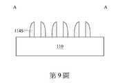
第9圖是根據本發明的一些實施例,繪示出字元線布局之剖面示意圖。FIG. 9 is a schematic cross-sectional view showing the layout of character lines according to some embodiments of the present invention.
第10及11圖是根據本發明的一些實施例,繪示出字元線布局之上視圖。Figures 10 and 11 are top views showing the layout of character lines according to some embodiments of the present invention.
第12圖是根據本發明的一些實施例,繪示出字元線布局之剖面示意圖。FIG. 12 is a schematic cross-sectional view showing the layout of character lines according to some embodiments of the present invention.
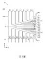
第1至3圖是根據本發明的一些實施例,繪示出字元線布局的上視圖。參照第1圖,字元線布局10包括:基底100、第一字元線組G1、第二字元線組G2、及I型第三字元線103。第一字元線組G1位於基底100上,且包括複數個L型第一字元線101。第二字元線組G2位於基底100上,且包括複數個L型第二字元線102。第一字元線組G1與第二字元線組G2並列設置,且沿平行於第二方向X的對稱軸S互相對稱。I型第三字元線103設置於第一字元線組G1與第二字元線組G2之外側,且沿第一方向Y延伸並跨過對稱軸S。一些實施例中,字元線布局10內的所有字元線皆沿對稱軸S對稱。應理解的是,圖式中所繪示的字元線數量僅是作為示例,而非用以限定本發明實施例,且字元線之兩端皆可延伸與其他部件連接,或字元線之其中一端可延伸與其他部件連接。Figures 1 to 3 are top views illustrating the layout of character lines according to some embodiments of the present invention. Referring to FIG. 1, the
第2圖進一步繪示第1圖之字元線布局10的局部示意圖,為使圖式簡潔以方便說明,僅繪示I型第三字元線103及一組互相對稱的L型第一字元線101及L型第二字元線102。參照第2圖,每個第一字元線101具有互相連接的第一線段101P1及第二線段101P2,其中第一線段101P1沿第一方向Y延伸,第二線段101P2沿第二方向X延伸,且第一方向Y垂直第二方向X。類似地,每個第二字元線102具有互相連接的第一線段102P1及第二線段102P2,其中第一線段102P1沿第一方向Y延伸,第二線段102P2沿第二方向X延伸。一些實施例中,上述的I型第三字元線103設置於第一字元線組G1與第二字元線組G2之外側係指I型第三字元線103設置於第一字元線組G1與第二字元線組G2在第二方向X之反向上(亦即-X方向)的一側。根據本發明的一些實施例,第一字元線組G1之互相連接的第一線段101P1與第二線段101P2於鄰近對稱軸S的位置互相連接,且第二字元線組G2之互相連接的第一線段102P1與第二線段102P2也於鄰近對稱軸S的位置互相連接。參照第一圖,在此些實施例中,第一字元線組G1的第一線段101P1與相應的第二線段101P2互相連接的位置隨第一字元線101遠離第三字元線103而遠離對稱軸S,且第二字元線組G2的第一線段102P1與相應的第二線段102P2互相連接的位置隨第二字元線102遠離第三字元線103而遠離對稱軸S。Figure 2 further shows a partial schematic diagram of the
再參照第1及2圖,一些實施例中,在第一字元線組G1中,在第一方向Y或第二方向X上相鄰的第一字元線101的間距相等,且在第二字元線組G2中,在第一方向Y或第二方向X上相鄰的第二字元線120的間距相等。詳細而言,在第一字元線組G1中,相鄰的第一線段101P1具有相同的間距W1,且相鄰的第二線段101P2具有相同的間距W2,而由於第一字元線組G1與第二字元線組G2沿對稱軸S互相對稱,因此在第二字元線組G2中,相鄰的第一線段102P1也具有相同的間距W1,且相鄰的第二線段102P2也具有相同的間距W2。根據本發明的一些實施例,間距W1大於20nm,且間距W2大於20nm。且在其他實施例中,第一字元線組G1中相鄰的第一線段101P1可具有不同的間距且相鄰的第二線段101P2也可具有不同的間距,而由於第一字元線組G1與第二字元線組G2沿對稱軸S互相對稱,因此在第二字元線組G2中,相鄰的第一線段102P1的間距及相鄰的第二線段102P2的間距分別與相對稱的第一字元線組G1中相鄰的第一線段101P1及相鄰的第二線段101P2之間距相同。Referring again to FIGS. 1 and 2, in some embodiments, in the first character line group G1, the distance between adjacent
一些實施例中,第三字元線103與第一字元線組G1及第二字元線組G2的間距W3大於或等於此些第一字元線101中相鄰的兩個第一線段101P1的間距W1及此些第二字元線102中相鄰的兩個第一線段102P1的間距W1。在一實施例中,間距W3可大於間距W1且間距W1大於20nm,在此情況下,第三字元線103可能因較遠離第一字元線組G1及第二字元線組G2,而未顯示於字元線布局的局部上視圖中。其他實施例中,在第一字元線101中,相鄰的兩個第一線段101P1之間距W1大於相鄰的兩個第二線段101P2之間距W2,且在第二字元線102中,相鄰的兩個第一線段102P1之間距W1大於相鄰的兩個第二線段102P2之間距W2。In some embodiments, the distance W3 between the
詳細而言,在字元線布局10中,設置於第一字元線組G1與第二字元線組G2之外側的第三字元線103,可使第一字元線組G1及第二字元線組G2的邊緣處不處於疏離環境,如前所述,可提昇製程容忍度或產率,並且可避免第一字元線組G1與第二字元線組G2在製程中發生斷裂或頸縮。在進一步的實施例中,可調整第三字元線103與第一字元線組G1及第二字元線組G2的間距W3、或第一字元線組G1及第二字元線組G2中的線段間距W1或W2,以達到對稱、均勻、或密集的字元線布局,以達到在不同製程條件或設計需求下,仍可提昇製程容忍度或產率,且避免字元線斷裂或頸縮。In detail, in the
參照第2圖,第一字元線101可具有連接線段101C,以連接第一線段101P1與第二線段101P2,且第二字元線102可具有連接線段102C,以連接第一線段102P1與第二線段102P2。在第2圖的示例中,連接線段101C及102C為直線。在其他實施例中,連接線段101C及102C為曲線,如第3圖所示。又或者第一字元線101的第一線段101P1與第二線段101P2可直接連接,且第二字元線102的第一線段102P1與第二線段102P2的連接處可直接連接,而不存在連接線段101C及102C,如第4圖所示。Referring to FIG. 2, the
參照第5圖,字元線布局10可包括複數個保護層104,設置於第一字元線101的第一線段101P1及第二字元線102的第一線段102P1上。一些實施例中,保護層104的材料包括未摻雜的矽。在其他實施例中,保護層104亦設置於第三字元線103上。在一些實施例中,第一字元線101、第二字元線102、及保護層104的材料可包括:碳、氮氧化矽、氮化物、氧化物、氧化物-氮化物-氧化物(ONO)、多晶矽、鈷、矽化鈷(CoSi2)、金屬、及阻抗材料。一些實施例中,第一字元線101及第二字元線102的材料不同於保護層104的材料。Referring to FIG. 5, the
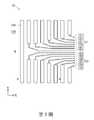
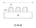
第6A及8A圖是根據本發明的一些實施例,繪示出形成字元線布局之中間階段的上視圖。第6B、7、及8B圖是根據本發明的一些實施例,繪示出形成字元線布局之中間階段的剖面示意圖。第6B圖為第6A圖中的結構沿直線AA的剖面示意圖。參照第6A及6B圖,提供基底100,形成遮罩材料層於基底100上並將其圖案化,以形成圖案化遮罩層110。如第6A圖所示,圖案化遮罩層110包括複數個L型第一遮罩111、複數個L型第二遮罩112、及T型第三遮罩113。前述複數個L型第一遮罩111與複數個L型第二遮罩112並列設置且互相對稱,且部分T型第三遮罩113設置於前述複數個L型第一遮罩111與L型第二遮罩112之間。應理解的是,圖式中所繪示的遮罩數量僅是作為示例,而非用以限定本發明。FIGS. 6A and 8A are top views illustrating an intermediate stage of forming a character line layout according to some embodiments of the present invention. FIGS. 6B, 7 and 8B are schematic cross-sectional views illustrating the intermediate stage of forming the character line layout according to some embodiments of the present invention. Figure 6B is a schematic cross-sectional view of the structure in Figure 6A along line AA. Referring to FIGS. 6A and 6B, a
一些實施例中,基底100可包括:元素半導體,包括矽或鍺;化合物半導體,包括砷化鎵(GaAs)、磷化鎵(GaP)、磷化銦(InP)、砷化銦(InAs)及/或銻化銦(InSb);合金半導體,包括矽鍺合金、磷砷鎵合金、砷鋁銦合金、砷鋁鎵合金、砷銦鎵合金、磷銦鎵合金及/或磷砷銦鎵合金、或前述材料之組合。其他實施例中,基底100可包括:碳、氮氧化矽、氮化物、氧化物、氧化物、氧化物-氮化物-氧化物(ONO)、多晶矽、鈷、矽化鈷(CoSi2)、金屬、及阻抗材料。圖案化遮罩層110的材料可包括:氧化物、氮化物(例如氮化矽)、氮氧化物(例如氮氧化矽)、或其他適合的材料,例如四乙氧基矽烷(tetraethyl orthosilicate,TEOS)、碳、氧化物-氮化物-氧化物(ONO)、多晶矽、鈷、矽化鈷(CoSi2)、金屬、及阻抗材料,且可使用沉積製程來形成,例如:化學氣相沉積(CVD)、物理氣相沉積(PVD)、原子層沉積(ALD)、旋轉塗佈(spin-on coating)等等。In some embodiments, the
第6C圖是根據一些實施例,繪示出圖案化遮罩層110的局部示意圖。為使圖式簡潔以方便說明,僅繪示T型第三遮罩113及一組互相對稱的L型第一遮罩111及L型第二遮罩112。參照第6C圖,每個L型第一遮罩111具有互相連接的第一部分111P1及第二部分111P2,第一部分111P1沿第一方向Y延伸,第二部分111P2沿第二方向X延伸。每個L型第二遮罩112具有互相連接的第一部分112P1及第二部分112P2,第一部分112P1沿第一方向Y延伸,第二部分112P2沿第二方向X延伸,且所述L型第一遮罩111與所述L型第二遮罩112沿平行於第二方向X的對稱軸S互相對稱。T型第三遮罩113包括互相連接的第一部分113P1及第二部分113P2,第一部分113P1設置於L型第一遮罩111與L型第二遮罩112之外側,沿第一方向Y延伸並跨過對稱軸S,且第二部分113P2設置於對稱軸S上,沿第二方向X延伸。此處的外側係指T型第三遮罩113的第一部分113P1設置於L型第一遮罩111與L型第二遮罩112在第二方向X之反向上(亦即-X方向)的一側。根據本發明的一些實施例,圖案化遮罩層110為對稱結構且具有奇數個遮罩,舉例而言,在第6A圖中,圖案化遮罩層110可包括複數個L型第一遮罩111、複數個L型第二遮罩112、及一個T型第三遮罩113,因為複數個L型第一遮罩111與複數個L型第二遮罩112沿對稱軸S互相對稱,所以L型第一遮罩111的數量(例如n個)與L型第二遮罩112的數量相同,其數量和為2的倍數(2n個),並加上一個T型第三遮罩113,因此圖案化遮罩層110的遮罩數量為奇數(2n+1)。FIG. 6C is a partial schematic diagram illustrating the patterned
參照第6A及6C圖,一些實施例中,T型第三遮罩113的第一部分113P1與所述複數個L型第一遮罩111及L型第二遮罩112的間距D3等於所述複數個L型第一遮罩111中相鄰的兩個第一部分111P1之間距D1及所述複數個L型第二遮罩112中相鄰的兩個第一部分112P1之間距D1。一些實施例中,所述複數個L型第一遮罩111中相鄰的兩個第二部分111P2之間距D2及所述複數個L型第二遮罩112中相鄰的兩個第二部分112P2之間距D2小於前述的間距D1。在第6A圖所示的一些實施例中,所述間距D1大於20nm、間距D2大於20nm、且間距D3大於20nm。一些實施例中,L型第一遮罩111的第一部分111P1及L型第二遮罩112的第一部分112P1的寬度W4等於前述的間距D3以及T型第三遮罩113的第一部分113P1的寬度W6。一些實施例中,L型第一遮罩111的第一部分111P1及L型第二遮罩112的第一部分112P1的寬度W4大於L型第一遮罩111的第二部分111P2及L型第二遮罩112的第二部分112P2的寬度W5。在第6C圖所示的一些實施例中,所述寬度W4大於20nm、寬度W5大於20nm、且寬度W6大於20nm。根據本發明的一些實施例,T型第三遮罩113的設計為中間較寬而兩側較窄,舉例而言,參照第6C圖,T型第三遮罩113的中間部分在第二方向X上的寬度範圍介於W6與W7之間(其中寬度W7大於W6,且寬度W7可大於30nm),其大於兩側的T型第三遮罩113的第一部分113P1的寬度W6,前述配置可使裝置在低電阻態(Low Resistance State,LRS)時得到較大的電流,而在高電阻態(High Resistance State,HRS)時可得到較小的電流值。Referring to FIGS. 6A and 6C, in some embodiments, the distance D3 between the first portion 113P1 of the T-shaped
接著參照第7圖,順應性沉積間隔物材料層114於基底100上及圖案化遮罩層110的頂表面和側壁上。間隔物材料層114的材料包括:氧化物、氮化物、或多晶矽。間隔物材料層114的沉積製程可包括:化學氣相沉積、物理氣相沉積、原子層沉積、旋轉塗佈等等。Next, referring to FIG. 7, a
參照第8A及8B圖,第8B圖為第8A圖中的結構沿直線AA的剖面示意圖,蝕刻間隔物材料層114,露出部分基底100之頂表面及圖案化遮罩層110的頂表面,以形成複數個間隔物114S於圖案化遮罩層110的側壁上。詳細而言,前述蝕刻製程移除部分基底100的頂表面及圖案化遮罩層110的頂表面上的間隔物材料層114。如第8A圖所示,間隔物114S形成於L型第一遮罩111、L型第二遮罩112、以及T型第三遮罩113的側壁上。一些實施例中,蝕刻製程可包括:反應式離子蝕刻(RIE)、中性粒子束蝕刻(NBE)、感應耦合電漿蝕刻(inductive coupled plasma etch)、其他適合的蝕刻製程、或前述之組合。Referring to Figures 8A and 8B, Figure 8B is a schematic cross-sectional view of the structure in Figure 8A along line AA. The
參照第1及9圖,移除圖案化遮罩層110並留下間隔物114S,形成如第1圖所示的字元線布局10。第9圖為第1圖所示的字元線布局10沿直線AA的剖面示意圖。一些實施例中,可使用前述的蝕刻製程來移除圖案化遮罩層110,也可使用剝離(strip)製程、灰化(ash)製程、或前述之組合。Referring to FIGS. 1 and 9, the patterned
本發明實施例之字元線布局的形成方法,提供具有對稱性的圖案化遮罩層,使所欲的間隔物(或字元線)在製程中不處於疏離的環境,可避免所欲的間隔物在製程中斷裂或頸縮,以提昇裝置的性能和可靠度。舉例而言,參照第8A圖,在T型第三遮罩113遠離L型第一遮罩111及L型第二遮罩112之側壁上的間隔物,可使在T型第三遮罩113靠近L型第一遮罩111及L型第二遮罩112之側壁上的間隔物在製程中不處於疏離的環境,以避免因疏離環境的製程條件不同造成的斷裂或頸縮。一些實施例中,在T型第三遮罩113遠離L型第一遮罩111及L型第二遮罩112之側壁上的間隔物也可稱為輔助間隔物,此輔助間隔物對應於移除圖案化遮罩層110後形成的字元線布局10中的第三字元線103。The method for forming the character line layout of the embodiment of the present invention provides a patterned mask layer with symmetry, so that the desired spacers (or character lines) are not in the manufacturing process.Being in an isolated environment can prevent the desired spacer from breaking or necking during the manufacturing process, so as to improve the performance and reliability of the device. For example, referring to FIG. 8A, the spacers on the sidewalls of the T-shaped
本發明實施例之字元線布局的形成方法,還提供了具有奇數個遮罩的對稱圖案化遮罩層(例如第6A圖所繪示的實施例),使所欲的間隔物不處於疏離環境或非對稱結構,亦具有前述的技術效果。The method for forming the character line layout of the embodiment of the present invention also provides a symmetrically patterned mask layer with an odd number of masks (for example, the embodiment shown in FIG. 6A), so that the desired spacers are not separated from each other. The environment or asymmetric structure also has the aforementioned technical effects.
一些實施例中,在移除圖案化遮罩層110以形成第1圖所示的字元線布局10之後,可移除第三字元線103,以形成如第10圖所示的字元線布局20,字元線布局20與字元線布局10的配置類似,其中字元線布局20不包含第三字元線103。一些實施例中,可形成複數個保護層104於字元線布局20的L型第一字元線101的第一線段101P1上及L型第二字元線102的第一線段102P1上,如第11及12圖所示,第12圖為第11圖所示的字元線布局20沿直線AA的剖面示意圖。一些實施例中,第12圖為第5圖所示的字元線布局10沿直線AA的剖面示意圖。除了前述的效果外,此些實施例中的保護層104可在後續的製程階段中保護下方部件,或作為遮罩。In some embodiments, after the patterned
綜上所述,本發明實施例提供字元線布局,包括對稱性的字元線布局,可避免字元線在製程中斷裂或頸縮,並提升裝置可靠度、製程容忍度、或產率。本發明實施例亦提供字元線布局的形成方法,包括形成對稱性的圖案化遮罩層,可在圖案化製程期間提供不疏離的環境,以避免字元線斷裂或頸縮,具有改善製程容忍度的效果。In summary, the embodiments of the present invention provide character line layouts, including symmetrical character line layouts, which can prevent character lines from breaking or necking during the manufacturing process, and improve device reliability, process tolerance, or productivity . The embodiment of the present invention also provides a method for forming a character line layout, including forming a symmetrical patterned mask layer, which can provide a non-distancing environment during the patterning process to avoid breakage or necking of the character line, and improve the process The effect of tolerance.
20:字元線布局20: Character line layout
100:基底100: base
101:第一字元線101: The first character line
102:第二字元線102: Second character line
G1:第一字元線組G1: The first character line group
G2:第二字元線組G2: The second character line group
S:對稱軸S: axis of symmetry
Claims (10)
Translated fromChinesePriority Applications (2)
| Application Number | Priority Date | Filing Date | Title |
|---|---|---|---|
| TW109143020ATWI746303B (en) | 2020-12-07 | 2020-12-07 | Layout of wordline and method of forming the same |
| US17/345,391US11515252B2 (en) | 2020-12-07 | 2021-06-11 | Layout of wordline and method of forming the same |
Applications Claiming Priority (1)
| Application Number | Priority Date | Filing Date | Title |
|---|---|---|---|
| TW109143020ATWI746303B (en) | 2020-12-07 | 2020-12-07 | Layout of wordline and method of forming the same |
Publications (2)
| Publication Number | Publication Date |
|---|---|
| TWI746303Btrue TWI746303B (en) | 2021-11-11 |
| TW202223896A TW202223896A (en) | 2022-06-16 |
Family
ID=79907667
Family Applications (1)
| Application Number | Title | Priority Date | Filing Date |
|---|---|---|---|
| TW109143020ATWI746303B (en) | 2020-12-07 | 2020-12-07 | Layout of wordline and method of forming the same |
Country Status (2)
| Country | Link |
|---|---|
| US (1) | US11515252B2 (en) |
| TW (1) | TWI746303B (en) |
Families Citing this family (2)
| Publication number | Priority date | Publication date | Assignee | Title |
|---|---|---|---|---|
| US20190390341A1 (en)* | 2018-06-26 | 2019-12-26 | Lam Research Corporation | Deposition tool and method for depositing metal oxide films on organic materials |
| TWI746303B (en)* | 2020-12-07 | 2021-11-11 | 華邦電子股份有限公司 | Layout of wordline and method of forming the same |
Citations (4)
| Publication number | Priority date | Publication date | Assignee | Title |
|---|---|---|---|---|
| US20080106922A1 (en)* | 2006-11-02 | 2008-05-08 | Joon-Min Park | Semiconductor memory device and layout structure of word line contacts |
| US8406028B1 (en)* | 2011-10-31 | 2013-03-26 | Taiwan Semiconductor Manufacturing Co., Ltd. | Word line layout for semiconductor memory |
| US20160099248A1 (en)* | 2013-05-16 | 2016-04-07 | Ps5 Luxco S.A.R.L. | Semiconductor memory device with improved active area/word line layout |
| CN110349960A (en)* | 2019-07-08 | 2019-10-18 | 上海华虹宏力半导体制造有限公司 | The domain structure of embedded flash memory, embedded flash memory and forming method thereof |
Family Cites Families (18)
| Publication number | Priority date | Publication date | Assignee | Title |
|---|---|---|---|---|
| TW503396B (en)* | 1999-12-03 | 2002-09-21 | Hitachi Ltd | Semiconductor device |
| TW519738B (en)* | 2001-12-05 | 2003-02-01 | Winbond Electronics Corp | Extended type capacitor manufacturing method and device of memory |
| KR100454131B1 (en)* | 2002-06-05 | 2004-10-26 | 삼성전자주식회사 | Semiconductor device having line-shaped patterns and method for layout for the same |
| US6905930B2 (en)* | 2003-11-14 | 2005-06-14 | United Microelectronics Corp. | Memory device and fabrication method thereof |
| KR100614660B1 (en)* | 2005-06-01 | 2006-08-22 | 삼성전자주식회사 | Data line of semiconductor memory device and forming method thereof |
| KR20070092549A (en) | 2006-03-10 | 2007-09-13 | 주식회사 하이닉스반도체 | How to insert an auxiliary pattern into the exposure mask |
| KR100801742B1 (en) | 2006-06-29 | 2008-02-11 | 주식회사 하이닉스반도체 | How to form a photo mask |
| KR101618749B1 (en)* | 2009-02-27 | 2016-05-09 | 삼성전자주식회사 | Method of forming patterns for semiconductor device |
| US8461053B2 (en)* | 2010-12-17 | 2013-06-11 | Spansion Llc | Self-aligned NAND flash select-gate wordlines for spacer double patterning |
| US8728940B2 (en)* | 2012-01-26 | 2014-05-20 | Micron Technology, Inc. | Memory arrays and methods of forming same |
| US9806093B2 (en)* | 2015-12-22 | 2017-10-31 | Sandisk Technologies Llc | Through-memory-level via structures for a three-dimensional memory device |
| KR102432379B1 (en)* | 2017-10-16 | 2022-08-12 | 삼성전자주식회사 | Semiconductor device |
| US11018151B2 (en)* | 2018-09-26 | 2021-05-25 | Sandisk Technologies Llc | Three-dimensional flat NAND memory device including wavy word lines and method of making the same |
| US20200371426A1 (en)* | 2019-05-22 | 2020-11-26 | Winbond Electronics Corp. | Anti-static photomask |
| US10872857B1 (en)* | 2019-06-18 | 2020-12-22 | Sandisk Technologies Llc | Three-dimensional memory device containing through-array contact via structures between dielectric barrier walls and methods of making the same |
| KR102732446B1 (en)* | 2020-01-17 | 2024-11-21 | 삼성전자주식회사 | Wiring structures and vertical memory devices including the same |
| TWI754408B (en)* | 2020-10-06 | 2022-02-01 | 華邦電子股份有限公司 | Method for forming semiconductor memory structure |
| TWI746303B (en)* | 2020-12-07 | 2021-11-11 | 華邦電子股份有限公司 | Layout of wordline and method of forming the same |
- 2020
- 2020-12-07TWTW109143020Apatent/TWI746303B/enactive
- 2021
- 2021-06-11USUS17/345,391patent/US11515252B2/enactiveActive
Patent Citations (4)
| Publication number | Priority date | Publication date | Assignee | Title |
|---|---|---|---|---|
| US20080106922A1 (en)* | 2006-11-02 | 2008-05-08 | Joon-Min Park | Semiconductor memory device and layout structure of word line contacts |
| US8406028B1 (en)* | 2011-10-31 | 2013-03-26 | Taiwan Semiconductor Manufacturing Co., Ltd. | Word line layout for semiconductor memory |
| US20160099248A1 (en)* | 2013-05-16 | 2016-04-07 | Ps5 Luxco S.A.R.L. | Semiconductor memory device with improved active area/word line layout |
| CN110349960A (en)* | 2019-07-08 | 2019-10-18 | 上海华虹宏力半导体制造有限公司 | The domain structure of embedded flash memory, embedded flash memory and forming method thereof |
Also Published As
| Publication number | Publication date |
|---|---|
| TW202223896A (en) | 2022-06-16 |
| US20220181249A1 (en) | 2022-06-09 |
| US11515252B2 (en) | 2022-11-29 |
Similar Documents
| Publication | Publication Date | Title |
|---|---|---|
| US7368362B2 (en) | Methods for increasing photo alignment margins | |
| US8916441B2 (en) | FinFET device and methods of fabrication | |
| TWI746303B (en) | Layout of wordline and method of forming the same | |
| US20120171867A1 (en) | Method for fabricating fine pattern by using spacer patterning technology | |
| KR102112941B1 (en) | Semiconductor devices comprising conductive lines and method of forming semiconductor devices | |
| US10410886B2 (en) | Methods of fabricating a semiconductor device | |
| CN106356299A (en) | Semiconductor structure with self-aligned spacer and manufacturing method thereof | |
| JP2010258224A (en) | Nonvolatile semiconductor memory device and manufacturing method thereof | |
| TWI734530B (en) | Semiconductor structure and method for forming the same | |
| CN114765156B (en) | Word line layout and forming method thereof | |
| CN101236899A (en) | Method for manufacturing grid | |
| US11804381B2 (en) | Conductive wire structure | |
| US7429527B2 (en) | Method of manufacturing self-aligned contact openings | |
| US11068635B2 (en) | Method of designing a mask and method of manufacturing a semiconductor device using the same | |
| CN113611745A (en) | Manufacturing method of semiconductor device | |
| CN114678323A (en) | Semiconductor device and method of forming the same | |
| CN111261695B (en) | Semiconductor structures and methods of forming them | |
| CN115132777B (en) | Semiconductor structure, forming method thereof and memory | |
| TWI845239B (en) | Semiconductor structure and method for forming the same | |
| CN111640758A (en) | Semiconductor device and method of forming the same | |
| CN114068567B (en) | Semiconductor structure and method for forming the same | |
| US20240389321A1 (en) | Method of manufacturing memory device | |
| US20250324587A1 (en) | Semiconductor structure and method for forming the same | |
| US20250192041A1 (en) | Wiring structures and methods of manufacturing the same | |
| KR20090077195A (en) | Semiconductor device and manufacturing method |