TWI745842B - Micro-luminescence element, micro-luminescence diode and micro-luminescence diode transfer method - Google Patents
Micro-luminescence element, micro-luminescence diode and micro-luminescence diode transfer methodDownload PDFInfo
- Publication number
- TWI745842B TWI745842BTW109102770ATW109102770ATWI745842BTW I745842 BTWI745842 BTW I745842BTW 109102770 ATW109102770 ATW 109102770ATW 109102770 ATW109102770 ATW 109102770ATW I745842 BTWI745842 BTW I745842B
- Authority
- TW
- Taiwan
- Prior art keywords
- micro
- light
- emitting diode
- intermediate layer
- micro light
- Prior art date
Links
Images


Classifications
- H—ELECTRICITY
- H01—ELECTRIC ELEMENTS
- H01L—SEMICONDUCTOR DEVICES NOT COVERED BY CLASS H10
- H01L25/00—Assemblies consisting of a plurality of semiconductor or other solid state devices
- H01L25/03—Assemblies consisting of a plurality of semiconductor or other solid state devices all the devices being of a type provided for in a single subclass of subclasses H10B, H10D, H10F, H10H, H10K or H10N, e.g. assemblies of rectifier diodes
- H01L25/10—Assemblies consisting of a plurality of semiconductor or other solid state devices all the devices being of a type provided for in a single subclass of subclasses H10B, H10D, H10F, H10H, H10K or H10N, e.g. assemblies of rectifier diodes the devices having separate containers
- H01L25/13—Assemblies consisting of a plurality of semiconductor or other solid state devices all the devices being of a type provided for in a single subclass of subclasses H10B, H10D, H10F, H10H, H10K or H10N, e.g. assemblies of rectifier diodes the devices having separate containers the devices being of a type provided for in group H10H20/00
- H—ELECTRICITY
- H10—SEMICONDUCTOR DEVICES; ELECTRIC SOLID-STATE DEVICES NOT OTHERWISE PROVIDED FOR
- H10H—INORGANIC LIGHT-EMITTING SEMICONDUCTOR DEVICES HAVING POTENTIAL BARRIERS
- H10H20/00—Individual inorganic light-emitting semiconductor devices having potential barriers, e.g. light-emitting diodes [LED]
- H10H20/80—Constructional details
- H10H20/85—Packages
- H10H20/8506—Containers
- H—ELECTRICITY
- H01—ELECTRIC ELEMENTS
- H01L—SEMICONDUCTOR DEVICES NOT COVERED BY CLASS H10
- H01L21/00—Processes or apparatus adapted for the manufacture or treatment of semiconductor or solid state devices or of parts thereof
- H01L21/67—Apparatus specially adapted for handling semiconductor or electric solid state devices during manufacture or treatment thereof; Apparatus specially adapted for handling wafers during manufacture or treatment of semiconductor or electric solid state devices or components ; Apparatus not specifically provided for elsewhere
- H01L21/683—Apparatus specially adapted for handling semiconductor or electric solid state devices during manufacture or treatment thereof; Apparatus specially adapted for handling wafers during manufacture or treatment of semiconductor or electric solid state devices or components ; Apparatus not specifically provided for elsewhere for supporting or gripping
- H01L21/6835—Apparatus specially adapted for handling semiconductor or electric solid state devices during manufacture or treatment thereof; Apparatus specially adapted for handling wafers during manufacture or treatment of semiconductor or electric solid state devices or components ; Apparatus not specifically provided for elsewhere for supporting or gripping using temporarily an auxiliary support
- H—ELECTRICITY
- H10—SEMICONDUCTOR DEVICES; ELECTRIC SOLID-STATE DEVICES NOT OTHERWISE PROVIDED FOR
- H10H—INORGANIC LIGHT-EMITTING SEMICONDUCTOR DEVICES HAVING POTENTIAL BARRIERS
- H10H20/00—Individual inorganic light-emitting semiconductor devices having potential barriers, e.g. light-emitting diodes [LED]
- H10H20/01—Manufacture or treatment
- H10H20/011—Manufacture or treatment of bodies, e.g. forming semiconductor layers
- H10H20/018—Bonding of wafers
- H—ELECTRICITY
- H10—SEMICONDUCTOR DEVICES; ELECTRIC SOLID-STATE DEVICES NOT OTHERWISE PROVIDED FOR
- H10H—INORGANIC LIGHT-EMITTING SEMICONDUCTOR DEVICES HAVING POTENTIAL BARRIERS
- H10H20/00—Individual inorganic light-emitting semiconductor devices having potential barriers, e.g. light-emitting diodes [LED]
- H10H20/01—Manufacture or treatment
- H10H20/036—Manufacture or treatment of packages
- H—ELECTRICITY
- H10—SEMICONDUCTOR DEVICES; ELECTRIC SOLID-STATE DEVICES NOT OTHERWISE PROVIDED FOR
- H10H—INORGANIC LIGHT-EMITTING SEMICONDUCTOR DEVICES HAVING POTENTIAL BARRIERS
- H10H20/00—Individual inorganic light-emitting semiconductor devices having potential barriers, e.g. light-emitting diodes [LED]
- H10H20/80—Constructional details
- H10H20/84—Coatings, e.g. passivation layers or antireflective coatings
- H—ELECTRICITY
- H10—SEMICONDUCTOR DEVICES; ELECTRIC SOLID-STATE DEVICES NOT OTHERWISE PROVIDED FOR
- H10H—INORGANIC LIGHT-EMITTING SEMICONDUCTOR DEVICES HAVING POTENTIAL BARRIERS
- H10H20/00—Individual inorganic light-emitting semiconductor devices having potential barriers, e.g. light-emitting diodes [LED]
- H10H20/80—Constructional details
- H10H20/85—Packages
- H—ELECTRICITY
- H01—ELECTRIC ELEMENTS
- H01L—SEMICONDUCTOR DEVICES NOT COVERED BY CLASS H10
- H01L2221/00—Processes or apparatus adapted for the manufacture or treatment of semiconductor or solid state devices or of parts thereof covered by H01L21/00
- H01L2221/67—Apparatus for handling semiconductor or electric solid state devices during manufacture or treatment thereof; Apparatus for handling wafers during manufacture or treatment of semiconductor or electric solid state devices or components; Apparatus not specifically provided for elsewhere
- H01L2221/683—Apparatus for handling semiconductor or electric solid state devices during manufacture or treatment thereof; Apparatus for handling wafers during manufacture or treatment of semiconductor or electric solid state devices or components; Apparatus not specifically provided for elsewhere for supporting or gripping
- H01L2221/68304—Apparatus for handling semiconductor or electric solid state devices during manufacture or treatment thereof; Apparatus for handling wafers during manufacture or treatment of semiconductor or electric solid state devices or components; Apparatus not specifically provided for elsewhere for supporting or gripping using temporarily an auxiliary support
- H01L2221/68363—Apparatus for handling semiconductor or electric solid state devices during manufacture or treatment thereof; Apparatus for handling wafers during manufacture or treatment of semiconductor or electric solid state devices or components; Apparatus not specifically provided for elsewhere for supporting or gripping using temporarily an auxiliary support used in a transfer process involving transfer directly from an origin substrate to a target substrate without use of an intermediate handle substrate
- H—ELECTRICITY
- H01—ELECTRIC ELEMENTS
- H01L—SEMICONDUCTOR DEVICES NOT COVERED BY CLASS H10
- H01L2221/00—Processes or apparatus adapted for the manufacture or treatment of semiconductor or solid state devices or of parts thereof covered by H01L21/00
- H01L2221/67—Apparatus for handling semiconductor or electric solid state devices during manufacture or treatment thereof; Apparatus for handling wafers during manufacture or treatment of semiconductor or electric solid state devices or components; Apparatus not specifically provided for elsewhere
- H01L2221/683—Apparatus for handling semiconductor or electric solid state devices during manufacture or treatment thereof; Apparatus for handling wafers during manufacture or treatment of semiconductor or electric solid state devices or components; Apparatus not specifically provided for elsewhere for supporting or gripping
- H01L2221/68304—Apparatus for handling semiconductor or electric solid state devices during manufacture or treatment thereof; Apparatus for handling wafers during manufacture or treatment of semiconductor or electric solid state devices or components; Apparatus not specifically provided for elsewhere for supporting or gripping using temporarily an auxiliary support
- H01L2221/68381—Details of chemical or physical process used for separating the auxiliary support from a device or wafer
- H01L2221/68386—Separation by peeling
- H—ELECTRICITY
- H01—ELECTRIC ELEMENTS
- H01L—SEMICONDUCTOR DEVICES NOT COVERED BY CLASS H10
- H01L25/00—Assemblies consisting of a plurality of semiconductor or other solid state devices
- H01L25/03—Assemblies consisting of a plurality of semiconductor or other solid state devices all the devices being of a type provided for in a single subclass of subclasses H10B, H10D, H10F, H10H, H10K or H10N, e.g. assemblies of rectifier diodes
- H01L25/04—Assemblies consisting of a plurality of semiconductor or other solid state devices all the devices being of a type provided for in a single subclass of subclasses H10B, H10D, H10F, H10H, H10K or H10N, e.g. assemblies of rectifier diodes the devices not having separate containers
- H01L25/075—Assemblies consisting of a plurality of semiconductor or other solid state devices all the devices being of a type provided for in a single subclass of subclasses H10B, H10D, H10F, H10H, H10K or H10N, e.g. assemblies of rectifier diodes the devices not having separate containers the devices being of a type provided for in group H10H20/00
- H01L25/0753—Assemblies consisting of a plurality of semiconductor or other solid state devices all the devices being of a type provided for in a single subclass of subclasses H10B, H10D, H10F, H10H, H10K or H10N, e.g. assemblies of rectifier diodes the devices not having separate containers the devices being of a type provided for in group H10H20/00 the devices being arranged next to each other
- H—ELECTRICITY
- H10—SEMICONDUCTOR DEVICES; ELECTRIC SOLID-STATE DEVICES NOT OTHERWISE PROVIDED FOR
- H10H—INORGANIC LIGHT-EMITTING SEMICONDUCTOR DEVICES HAVING POTENTIAL BARRIERS
- H10H20/00—Individual inorganic light-emitting semiconductor devices having potential barriers, e.g. light-emitting diodes [LED]
- H10H20/01—Manufacture or treatment
- H10H20/034—Manufacture or treatment of coatings
Landscapes
- Engineering & Computer Science (AREA)
- Microelectronics & Electronic Packaging (AREA)
- Power Engineering (AREA)
- Physics & Mathematics (AREA)
- Condensed Matter Physics & Semiconductors (AREA)
- General Physics & Mathematics (AREA)
- Computer Hardware Design (AREA)
- Manufacturing & Machinery (AREA)
- Led Devices (AREA)
- Led Device Packages (AREA)
Abstract
Translated fromChineseDescription
Translated fromChinese本發明是有關於一種半導體製造領域,特別是指一種微發光元件、微發光二極體,及微發光二極體轉移方法。The present invention relates to the field of semiconductor manufacturing, in particular to a micro-light-emitting element, micro-light-emitting diode, and a method for transferring the micro-light-emitting diode.
微型發光二極體(Micro LED)是目前熱門研究的下一代顯示器的光源。微型發光二極體顯示器具有低功率消耗、高亮度、超高解析度、超高色彩飽和度、回應速度快、能耗低,及壽命長等優點。此外,微型發光二極體顯示器的功率消耗量約為液晶顯示器(LCD)的10%或有機發光二極體顯示器(OLED)的50%。而與同樣是自發光的OLED相比較,亮度高了30倍,且解析度可以達到1500PPI(像素密度,Pixels Per Inch)。微型發光二極體顯示器的的這些明顯的優勢,使得它有望取代現在的OLED和LCD,成為下一代的顯示器。微型發光二極體目前還無法量產,是因為目前還有許多技術難題需要克服,其中一個重要的技術難題就是如何提高轉印良率。Micro LED (Micro LED) is the light source of the next-generation display that is currently hotly researched. Miniature LED displays have the advantages of low power consumption, high brightness, ultra-high resolution, ultra-high color saturation, fast response speed, low energy consumption, and long life. In addition, the power consumption of a micro light emitting diode display is about 10% of that of a liquid crystal display (LCD) or 50% of an organic light emitting diode display (OLED). Compared with the self-luminous OLED, the brightness is 30 times higher, and the resolution can reach 1500PPI (Pixels Per Inch). These obvious advantages of the miniature light-emitting diode display make it expected to replace the current OLED and LCD and become the next-generation display. Miniature light-emitting diodes cannot be mass-produced at present because there are still many technical problems that need to be overcome. One of the important technical problems is how to improve the transfer yield.
例如天津三安光電有限公司的專利申請(公開號:CN107681034A)中提及的微發光製作技術,利用熱固性材料製作支撐柱支撐芯粒,使器件置於待拾取狀態,而在該案提供的器件基礎上通過壓模壓印方式巨量轉移芯粒。For example, the micro-luminescence manufacturing technology mentioned in the patent application of Tianjin San'an Optoelectronics Co., Ltd. (Publication No.: CN107681034A) uses thermosetting materials to make support columns to support the core particles, so that the device is placed in the state of being picked up, and the device provided in this case On the basis, a huge amount of core particles are transferred by means of stamping and imprinting.
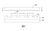
參看圖1和圖2,雖然該案工藝製作的器件可以用來對倒裝型微發光二極體100進行巨量轉移,但利用壓模壓印200對該器件進行壓印的過程中,由於熱固性材料製作的支撐柱310對微發光二極體100的粘附力大於支撐柱310內部本身的斷裂強度,支撐柱310在粘附力的外加載荷作用下,應力達到支撐柱310材料的斷裂強度而產生斷裂。該斷裂位置難以掌控,殘餘的支撐柱311附著在微發光二極體100表面,在一些情況下,該殘餘的支撐柱311高度高於微發光二極體100電極的高度,殘留高度太高就無法完成後續微發光二極體100的固晶工藝,嚴重影響了固晶工藝的良率。1 and 2, although the device manufactured by the process of this case can be used to transfer a large amount of the flip-chip
因此,本發明的第一目的,即在提供一種可以大幅減少在微發光二極體表面的支撐柱殘留的微發光元件。Therefore, the first object of the present invention is to provide a micro light emitting element that can greatly reduce the residual support posts on the surface of the micro light emitting diode.
於是,本發明微發光元件包含基架,包括柱狀結構;至少一個微發光二極體,在一些情況下可以由一系列微發光二極體組成陣列排布,微發光二極體通過柱狀結構而與基架連接,微發光二極體由柱狀結構提供支撐;柱狀結構與微發光二極體連接的一端位於微發光二極體表面的凹槽內,柱狀結構的材料為高分子聚合物。Therefore, the micro-light-emitting element of the present invention includes a base frame, including a columnar structure; at least one micro-light-emitting diode may be arranged in an array by a series of micro-light-emitting diodes in some cases, and the micro-light-emitting diodes pass through the columnar structure. The structure is connected to the base frame, and the micro-light-emitting diode is supported by the columnar structure; the end of the columnar structure connected to the micro-light-emitting diode is located in the groove on the surface of the micro-light-emitting diode, and the material of the columnar structure is high Molecular polymers.
本發明的第二目的,即在提供一種微發光二極體。該微發光二極體為上述微發光元件為待拾取狀態下的器件,且對該器件進行壓模壓印拾取轉移微發光元件而得。The second objective of the present invention is to provide a micro light emitting diode. The micro-light-emitting diode is a device in which the above-mentioned micro-light-emitting element is in a state to be picked up, and the micro-light-emitting element is picked up and transferred by stamping and embossing the device.
本發明微發光二極體,包含發光外延層,具有N型層、P型層和兩者之間的發光層;N型電極,與N型層連接;P型電極,與P型層連接;微發光二極體具有相對應的第一表面和第二表面,第一表面具有凹槽,凹槽用於容置一柱狀結構,一方面供該柱狀結構向微發光二極體傳遞支撐力,一方面提供與柱狀結構的粘附力,凹槽為第一中間層構成;第一中間層對高分子聚合物的粘合力大於高分子聚合物對發光外延層的粘合力。The micro light-emitting diode of the present invention includes a light-emitting epitaxial layer with an N-type layer, a P-type layer and a light-emitting layer between the two; an N-type electrode connected to the N-type layer; a P-type electrode connected to the P-type layer; The micro-light-emitting diode has a corresponding first surface and a second surface. The first surface has a groove. The groove is used to accommodate a columnar structure. On the one hand, the columnar structure can transfer support to the micro-light-emitting diode. On the one hand, it provides adhesion to the columnar structure, and the groove is composed of the first intermediate layer; the adhesion of the first intermediate layer to the high molecular polymer is greater than the adhesion of the high molecular polymer to the light-emitting epitaxial layer.
本發明的第三目的,即在提供一種用於巨量轉移微發光二極體的工藝方法。The third objective of the present invention is to provide a process method for mass transfer of micro light-emitting diodes.
本發明巨量微發光二極體轉移方法,包含以下步驟:步驟1,提供襯底,襯底上陣列式間隔排布有複數顆微發光二極體,在微發光二極體的表面及其之間裸露的襯底表面製作第一中間層;步驟2,在微發光二極體表面先沉積上犧牲材料,然後在犧牲材料和第一中間層上製作凹槽;步驟3,在犧牲材料上和第一中間層中的凹槽內製作第二中間層;步驟4,在第二中間層上製作支撐層;步驟5,提供一鍵合基架;步驟6,將鍵合基架和支撐層鍵合;步驟7,剝離襯底,裸露出微發光二極體和第一中間層;步驟8,依次去除裸露的第一中間層和犧牲材料。The method for transferring a large amount of micro-light-emitting diodes of the present invention includes the following steps: step 1, providing a substrate, on which a plurality of micro-light-emitting diodes are arranged at intervals in an array, on the surface of the micro-light-emitting diodes and The first intermediate layer is made on the exposed substrate surface; step 2, the sacrificial material is deposited on the surface of the micro light emitting diode, and then grooves are made on the sacrificial material and the first intermediate layer; step 3, on the sacrificial material And the groove in the first intermediate layer to make a second intermediate layer;
本發明的功效在於:在轉移過程中,減少或者消除微發光二極體上柱狀結構斷裂殘留,避免工藝殘留物過高影響後續微發光二極體共晶到電路板。The effect of the present invention is to reduce or eliminate the fracture residue of the columnar structure on the micro-light-emitting diode during the transfer process, and avoid excessive process residues from affecting the subsequent micro-light-emitting diode eutectic to the circuit board.
本發明的其它特徵和優點將在隨後的說明書中闡述,並且,部分地從說明書中變得顯而易見,或者通過實施本發明而瞭解。本發明的目的和其他優點可通過在說明書、申請專利範圍以及附圖中所特別指出的結構來實現和獲得。Other features and advantages of the present invention will be described in the following description, and partly become obvious from the description, or understood by implementing the present invention. The purpose and other advantages of the present invention can be realized and obtained through the structures specifically pointed out in the specification, the scope of the patent application and the drawings.
應當理解,本發明所使用的術語僅出於描述具體實施方式的目的,而不是旨在限制本發明。進一步理解,當在本發明中使用術語“包含”、"包括"時,用於表明陳述的特徵、整體、步驟、元件、和/或的存在,而不排除一個或多個其他特徵、整體、步驟、元件、和/或它們的組合的存在或增加。It should be understood that the terms used in the present invention are only for the purpose of describing specific embodiments, and are not intended to limit the present invention. It is further understood that when the terms "comprising" and "including" are used in the present invention, they are used to indicate the existence of the stated features, wholes, steps, elements, and/or without excluding one or more other features, wholes, The presence or addition of steps, elements, and/or combinations thereof.
在本發明被詳細描述前,應當注意在以下的說明內容中,類似的元件是以相同的編號來表示。Before the present invention is described in detail, it should be noted that in the following description, similar elements are denoted by the same numbers.
參看圖3,在本發明的實施例一中,提供一種微發光元件。該微發光元件包含具有穩固作用的基架,在本實施例中基架作為一個整體由藍寶石晶片320和旋塗的高分子聚合物構成,藍寶石晶片320也可以用玻璃和矽襯底替代,高分子聚合物作為支撐層330,例如由BCB膠(苯并環丁烯)構成,基架包括由BCB膠構成的柱狀結構310;至少一個微發光二極體100,以陣列式分佈為例,微發光二極體100通過柱狀結構310而與基架連接,微發光二極體100由柱狀結構310提供支撐;柱狀結構310與微發光二極體100連接的一端位於微發光二極體100表面,該表面優選為非出光表面。Referring to FIG. 3, in the first embodiment of the present invention, a micro light-emitting element is provided. The micro light-emitting element includes a base frame with a stable effect. In this embodiment, the base frame as a whole is composed of a
柱狀結構柱徑是一致的,例如圓柱結構。柱狀結構310的柱徑是變化的,例如柱狀結構310為柱徑上端小、下端大的凸台結構,與微發光二極體100接觸的一端的柱徑小於遠離微發光二極體100接觸的一端的柱徑,從上至下逐步變粗,該結構的優勢在於柱狀結構310與微發光二極體100的接觸面小,粘合力與接觸面積成正比,在保證柱狀結構310對微發光二極體100穩定支撐作用的前提下,降低兩者的粘合力,從上至下逐步變粗的柱狀結構310具有更強的斷裂強度,降低粘合力、增強斷裂強度降低柱狀結構310與微發光二極體100在壓模壓印作用下分離時斷裂的可能性,從而提高微發光二極體100拾取轉移的良率。The column diameter is the same in columnar structures, such as cylindrical structures. The column diameter of the
參看圖4,在本發明的實施例二中,提供一種微發光元件。該微發光元件的柱狀結構310的柱徑是變化的,且在柱狀結構310中設計應力集中區域,例如柱狀結構310具有一小面積截面,該小面積截面與其附近的截面相比具有更小的橫截面積。Referring to FIG. 4, in the second embodiment of the present invention, a micro light-emitting element is provided. The column diameter of the
具體來說,小面積截面與柱狀結構310的其他區域相比,具有更小的橫截面積,採用曲線型的柱狀結構310。該實施例中,小面積截面為柱狀結構310的應力集中面312,在壓模壓印對微發光元件中的微發光二極體100施加壓力,壓力從微發光二極體100傳導到柱狀結構310,柱狀結構310在應力集中面312斷裂,實現斷裂位置可控,應力集中面312的中心位置的高度可以設計低於電極的高度,保證斷裂後的柱狀結構低於電極的高度,保證在後續共晶鍵合工藝中殘餘的柱狀結構不干涉電極共晶。Specifically, the small-area cross-section has a smaller cross-sectional area than other regions of the
在實施例二的一個變形實施例中,在柱狀結構310中設計應力缺陷區域,應力缺陷區域實現柱狀結構310斷裂面的可控性,例如在柱狀結構310中設計多孔結構,應力缺陷區域的中心位置的高度可以設計低於電極的高度,保證斷裂後殘餘的柱狀結構低於電極的高度,保證在後續共晶鍵合工藝中殘餘的柱狀結構不干涉電極共晶。In a modified embodiment of the second embodiment, the stress defect area is designed in the
參看圖5,在本發明的實施例三中,在微發光二極體100與柱狀結構310之間加入第一中間層110,第一中間層110至少兼顧有過渡作用,由於微發光二極體100巨量轉移工藝中,難免涉及到蝕刻,蝕刻的化學反應會產生氣泡,氣泡對微發光二極體100產生衝擊力,以氮化鎵基微發光二極體為例,通常情況,氮化鎵與高分子聚合物的粘附性不佳,因此柱狀結構310和微發光二極體100之間的粘合需要得到充分的保障,而第一中間層110保證了微發光二極體100與柱狀結構310具有足夠的粘合力,由粘合力提供穩定的支撐,在本實施例中第一中間層110包括二氧化矽、氧化鋁或者氮化矽,高分子聚合物包括苯并環丁烯、矽膠或者紫外UV膠,相比氮化鎵,第一中間層110與高分子聚合物有更優良的粘附性。此外,第一中間層110對柱狀結構310的粘合力大於柱狀結構310對微發光二極體100的粘合力。Referring to FIG. 5, in the third embodiment of the present invention, a first
參看圖6,在本發明的實施例四中,在微發光二極體100與柱狀結構310之間加入第二中間層120,例如第二中間層120包括犧牲層,即在微發光二極體100與柱狀結構310之間加入犧牲層,在轉移過程中通過去除部分或者全部犧牲層,實現微發光二極體100與柱狀結構310的分離,選擇性去除工藝有助於保證微發光二極體100分離後無殘留柱狀結構,在轉移得到的微發光二極體100表面,僅殘留部分犧牲層材料或者完全無殘留,在本實施例中,犧牲層材料為光敏膠例如光阻或者紫外UV膠,也可以是二氧化矽等易於移除的材料。Referring to FIG. 6, in the fourth embodiment of the present invention, a second
本實施例中,在壓模壓印200對微發光二極體100轉移時,壓模壓印200先向下壓微發光二極體100,利用壓力產生粘附,接著利用粘附產生的吸力向上提起微發光二極體100,該吸力例如凡德瓦力。在本實施例中,第二中間層120對柱狀結構310的粘附力需小於柱狀結構310內的分子間作用力,即可保證第二中間層120與柱狀結構310脫離時,柱狀結構310內部不因為脫離時的拉力過大產生斷裂。In this embodiment, when the
參看圖7,在實施例四的第一個變形實施例中,第二中間層120的表面具有孔洞結構121,該孔洞結構121減小了第二中間層120與柱狀結構310的接觸面積,從而降低第二中間層120與柱狀結構310的脫離難度。具體來說,第二中間層120具有第一表面和第二表面,其中第一表面為上表面,位於靠近微發光二極體的一側,第二表面為下表面,位於靠近柱狀結構310的一側,孔洞結構121位於第一表面和/或第二表面。Referring to FIG. 7, in the first modified embodiment of the fourth embodiment, the surface of the second
跟本實施例相近的一種設計可應用於該實施例三中,即可以將第一中間層110遠離發光外延層的表面設計為多孔表面,多孔表面用於與柱狀結構310相連接,起到同樣的降低第一中間層110與柱狀結構310粘合力的作用。A design similar to this embodiment can be applied to the third embodiment, that is, the surface of the first
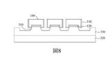
參看圖8,在實施例四的第二個變形實施例中,微發光元件既包括第一中間層110,也包括第二中間層120,第二中間層120包括跟第一中間層110粘附性較好的材料,以第一中間層110為二氧化矽製作的鈍化(passivation)保護層為例,第二中間層120選擇鉻或者鈦,第二中間層120與高分子聚合物的粘附性低於第一中間層110與高分子聚合物的粘附性,因此柱狀結構310較容易與第二中間層120脫離,脫離過程中,柱狀結構310不產生斷裂,脫離後的微發光二極體100上未見到高分子聚合物殘留。Referring to FIG. 8, in the second modified embodiment of the fourth embodiment, the micro light-emitting element includes both the first
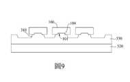
參看圖9,在本發明的實施例五中,為了在保證無高分子聚合物殘留的前提下簡化工藝,本實施例在微發光二極體100製作凹槽101,用於承接柱狀結構310,傳遞支撐力,柱狀結構310與界定出凹槽101的凹槽面104的底面部和側面部接觸。凹槽101位於微發光二極體100的非發光面一側或者直接位於非發光面上。Referring to FIG. 9, in the fifth embodiment of the present invention, in order to simplify the process under the premise of ensuring that there is no polymer residue, a
本實施例五具體工藝步驟包括步驟1至步驟9。The specific process steps of the fifth embodiment include step 1 to step 9.
參看圖10,步驟1,提供生長襯底130,生長襯底130通過光罩蝕刻出陣列式間隔排布的複數顆微發光二極體100,本實施例的微發光二極體100採用倒裝式結構,在微發光二極體100的表面及其之間裸露的生長襯底130表面製作第一中間層110,第一中間層110為PV保護層,材料包括二氧化矽、氧化鋁或者氮化矽。Referring to FIG. 10, step 1, a
步驟2,在微發光二極體100表面先沉積上犧牲材料140,然後在犧牲材料140和第一中間層110上製作凹槽101;在犧牲材料140和第一中間層110上凹槽101的深度為1000埃至2500埃。凹槽101的深度不宜太深,太深則粘附力過強,容易導致柱狀結構310斷裂,根據實驗結果最佳深度為1800埃至2000埃。Step 2:
步驟3,在犧牲材料140和第一中間層110中的凹槽101內製作第二中間層120;該第二中間層120較薄,圖中未標出犧牲材料140上的第二中間層120,並適當放大了凹槽101內第二中間層120的厚度,第二中間層120為鉻或者鈦。Step 3. A second
參看圖11,步驟4,在第二中間層120上製作支撐層330,例如採用高分子聚合物來形成該支撐層330,本實施例中高分子聚合物可選用BCB膠、紫外光敏膠或者光阻膠,在一些情況下,支撐層330也可以選用金屬,例如金、銦、鎳或者錫,支撐層330填充了凹槽101,形成柱狀結構310。Referring to FIG. 11,
步驟5,提供一鍵合基架321,在鍵合基架321待鍵合的一側也旋塗上膠層(圖未示),鍵合基架例如採用藍寶石、矽或者玻璃晶片。
步驟6,將鍵合基架321和支撐層330通過鍵合基架321的膠層鍵合。Step 6, bonding the
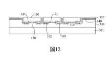
參看圖12,步驟7,剝離生長襯底130,例如採用雷射剝離工藝,移除生長襯底130後裸露出微發光二極體100和第一中間層110。Referring to FIG. 12, step 7, the
參看圖13和圖14,步驟8,依次去除裸露的第一中間層110、犧牲材料140以及其上的第二中間層120,使微發光二極體100獨立支撐在柱狀結構310上,至少保留部分凹槽101內的第二中間層120。該保留的第二中間層120由於位於凹槽101內,在去除過程中得以保留,構成了本實施例的微發光元件。13 and 14, step 8, sequentially remove the exposed first
參看圖15,步驟9,利用壓模壓印200對微發光二極體100遠離柱狀結構310的一面進行壓印,將微發光二極體100與柱狀結構310分離,拾取得微發光二極體100。Referring to FIG. 15, step 9, using stamping 200 to imprint the side of the micro
參看圖16和圖17,凹槽101內第二中間層120的高度低於微發光二極體100的P型電極102和N型電極103的高度,由於設置了凹槽101內的第二中間層120,保證了柱狀結構310與第一中間層110良好脫離,基本無柱狀結構310斷裂的情況。16 and 17, the height of the second
參看圖18,根據實施例五製備得到微發光二極體100,包含:發光外延層,具有N型層、P型層和兩者之間的發光層,因非關鍵要素未在圖中標示;P型電極102與P型層電連接;N型電極103與N型層電連接;微發光二極體100具有相對應的第一表面和第二表面,第一表面具有凹槽101,凹槽101用於與柱狀結構310對接,柱狀結構310於凹槽101內向微發光二極體100提供支撐,以倒裝微發光二極體100為例,凹槽101與兩個電極位於同面,凹槽101位於微發光二極體100的下表面,即不位於出光面上,避免降低出光效率。Referring to FIG. 18, a micro light-emitting
在凹槽101由第一中間層110構成,相對直接用發光外延層構成,第一中間層110具有足夠的粘合力。此外,第一中間層110對高分子聚合物的粘合力大於高分子聚合物對發光外延層的粘合力。凹槽101開口沿遠離發光外延層一側逐漸增大。The
第一中間層110包括二氧化矽、氧化鋁或者氮化矽,高分子聚合物包括苯并環丁烯、矽膠或者紫外UV膠。凹槽101的槽內具有第二中間層120。第二中間層120對高分子聚合物的粘附力,小於高分子聚合物內的分子間作用力。第二中間層120的材料包括鉻或者鈦。若凹槽101內殘留有高分子聚合物,則殘留的高分子聚合物的高度也不高於P型電極102和N型電極103。The first
綜上所述,在轉移過程中,減少或者消除微發光二極體上柱狀結構斷裂殘留,避免工藝殘留物過高影響後續微發光二極體共晶到電路板,故確實能達成本發明的目的。In summary, during the transfer process, the columnar structure fracture residue on the micro-light-emitting diode is reduced or eliminated, and the process residue is too high to affect the subsequent micro-light-emitting diode eutectic to the circuit board, so it can indeed achieve the cost of the invention. the goal of.
惟以上所述者,僅為本發明的實施例而已,當不能以此限定本發明實施的範圍,凡是依本發明申請專利範圍及專利說明書內容所作的簡單的等效變化與修飾,皆仍屬本發明專利涵蓋的範圍內。However, the above are only examples of the present invention. When the scope of implementation of the present invention cannot be limited by this, all simple equivalent changes and modifications made in accordance with the scope of the patent application of the present invention and the content of the patent specification still belong to Within the scope covered by the patent of the present invention.
100:微發光二極體101:凹槽104:凹槽面102:P型電極103:N型電極110:第一中間層120:第二中間層121:孔洞結構310:柱狀結構312:應力集中面321:鍵合基架320:藍寶石晶片330:支撐層200:壓模壓印130:生長襯底140:犧牲材料100: micro light emitting diode101: Groove104: Groove surface102: P-type electrode103: N-type electrode110: The first middle layer120: The second middle layer121: Hole structure310: Columnar structure312: Stress Concentration Surface321: Bonding base frame320: Sapphire wafer330: support layer200: stamping130: growth substrate140: Sacrificial Material
本發明的其他的特徵及功效,將於參照圖式的實施方式中清楚地呈現,其中:圖1~圖2為先前技術的巨量微發光二極體的轉移方法的示意圖;圖3為實施例一的微發光元件示意圖;圖4為實施例二的微發光元件示意圖;圖5為實施例三的微發光元件示意圖;圖6為實施例四的微發光元件示意圖;圖7~圖8為實施例四的變形實施例的微發光元件示意圖;圖9為實施例五的微發光元件示意圖;圖10~圖15為實施例五的微發光二極體轉移工藝示意圖;圖16~圖17為實施例五轉移得到的微發光二極體實物照片;及圖18為實施例五轉移得到的微發光二極體示意圖。Other features and effects of the present invention will be clearly presented in the embodiments with reference to the drawings, in which:Figures 1 to 2 are schematic diagrams of the transfer method of a huge amount of micro-light-emitting diodes in the prior art;Fig. 3 is a schematic diagram of the micro light emitting element of the first embodiment;4 is a schematic diagram of the micro light-emitting element of the second embodiment;Fig. 5 is a schematic diagram of the micro light-emitting element of the third embodiment;Fig. 6 is a schematic diagram of a micro light-emitting element of the fourth embodiment;7 to 8 are schematic diagrams of the micro light-emitting element of a modified embodiment of the fourth embodiment;Fig. 9 is a schematic diagram of the micro light-emitting element of the fifth embodiment;10 to 15 are schematic diagrams of the transfer process of the micro light-emitting diode according to the fifth embodiment;Figures 16 to 17 are photos of the micro light-emitting diodes transferred in Example 5; andFig. 18 is a schematic diagram of a micro light emitting diode obtained by transferring in Example 5.
100:微發光二極體100: micro light emitting diode
102:P型電極102: P-type electrode
103:N型電極103: N-type electrode
110:第一中間層110: The first middle layer
120:第二中間層120: The second middle layer
310:柱狀結構310: Columnar structure
321:鍵合基架321: Bonding base frame
330:支撐層330: support layer
Claims (32)
Translated fromChineseApplications Claiming Priority (2)
| Application Number | Priority Date | Filing Date | Title |
|---|---|---|---|
| PCT/CN2019/079577WO2020191593A1 (en) | 2019-03-25 | 2019-03-25 | Micro light emitting assembly, micro light emitting diode, and transfer printing method for micro light emitting diode |
| WOPCT/CN2019/079577 | 2019-03-25 |
Publications (2)
| Publication Number | Publication Date |
|---|---|
| TW202036931A TW202036931A (en) | 2020-10-01 |
| TWI745842Btrue TWI745842B (en) | 2021-11-11 |
Family
ID=70202062
Family Applications (1)
| Application Number | Title | Priority Date | Filing Date |
|---|---|---|---|
| TW109102770ATWI745842B (en) | 2019-03-25 | 2020-01-30 | Micro-luminescence element, micro-luminescence diode and micro-luminescence diode transfer method |
Country Status (6)
| Country | Link |
|---|---|
| US (1) | US20220005794A1 (en) |
| JP (1) | JP7154371B2 (en) |
| KR (2) | KR102544715B1 (en) |
| CN (1) | CN111033737B (en) |
| TW (1) | TWI745842B (en) |
| WO (1) | WO2020191593A1 (en) |
Families Citing this family (15)
| Publication number | Priority date | Publication date | Assignee | Title |
|---|---|---|---|---|
| TWI759839B (en)* | 2020-08-31 | 2022-04-01 | 錼創顯示科技股份有限公司 | Micro-led display device and manufacturing method of the same |
| DE102020102952B4 (en)* | 2020-02-05 | 2024-09-19 | OSRAM Opto Semiconductors Gesellschaft mit beschränkter Haftung | METHOD FOR SELECTING SEMICONDUCTOR COMPONENTS |
| WO2022006723A1 (en)* | 2020-07-06 | 2022-01-13 | 重庆康佳光电技术研究院有限公司 | Led chip transfer method, display back plate and fabricating method therefor, and display device |
| CN112018145B (en)* | 2020-08-31 | 2023-06-27 | 錼创显示科技股份有限公司 | Micro light emitting diode display assembly and manufacturing method thereof |
| CN112366247B (en)* | 2020-10-22 | 2021-10-08 | 中国电子科技集团公司第五十五研究所 | A kind of preparation method of transfer printing integrated top incident InGaAs detector |
| EP4174963A4 (en)* | 2020-10-30 | 2023-08-23 | BOE Technology Group Co., Ltd. | Light emitting diode substrate and manufacturing method therefor, and display apparatus |
| CN114122050A (en)* | 2020-11-23 | 2022-03-01 | 伊乐视有限公司 | Mass transfer method for microscopic light-emitting diode displays based on fluidic assembly |
| CN112510127B (en)* | 2020-12-21 | 2022-04-05 | 厦门大学 | Manufacturing method of suspension LED device |
| EP4275232A4 (en)* | 2021-01-08 | 2024-10-16 | Jade Bird Display (Shanghai) Limited | Systems and methods for led structures that increase current flow density |
| CN113421954B (en)* | 2021-05-21 | 2023-06-09 | 友达光电股份有限公司 | Display device and method for manufacturing the same |
| CN115706131B (en)* | 2021-08-10 | 2025-02-18 | 重庆康佳光电科技有限公司 | Huge amount transfer method, temporary substrate, transfer substrate and LED display device |
| CN116013945A (en)* | 2021-10-21 | 2023-04-25 | 重庆康佳光电技术研究院有限公司 | Weakened structure and manufacturing method thereof, transfer method of light-emitting device |
| KR20240119922A (en)* | 2023-01-30 | 2024-08-07 | 삼성전자주식회사 | Micro light emitting diode chip and method for manufacturing thereof |
| CN116207126B (en)* | 2023-03-27 | 2025-07-25 | 天马新型显示技术研究院(厦门)有限公司 | Micro-light-emitting element array, micro-light-emitting element transferring method and display device |
| WO2025116062A1 (en)* | 2023-11-28 | 2025-06-05 | 엘지전자 주식회사 | Transfer method of semiconductor light-emitting device for display pixels |
Citations (6)
| Publication number | Priority date | Publication date | Assignee | Title |
|---|---|---|---|---|
| TW201327911A (en)* | 2011-11-18 | 2013-07-01 | Luxvue Technology Corp | Method of forming a micro light emitting diode array |
| TW201330320A (en)* | 2011-11-18 | 2013-07-16 | Luxvue Technology Corp | Method for forming a micro-light emitting diode structure and an array of micro-light emitting diode structures having an electrically insulating layer |
| US20150372052A1 (en)* | 2014-06-18 | 2015-12-24 | X-Celeprint Limited | Micro assembled led displays and lighting elements |
| TW201622102A (en)* | 2014-10-17 | 2016-06-16 | 英特爾股份有限公司 | Micro LED display and assembly |
| US20160336486A1 (en)* | 2015-05-13 | 2016-11-17 | Au Optronics Corporation | Micro-light-emitting diode device and method for manufacturing the same |
| TW201841392A (en)* | 2017-02-10 | 2018-11-16 | 南韓商流明斯有限公司 | Micro light emitting diode module and manufacturing method thereof |
Family Cites Families (25)
| Publication number | Priority date | Publication date | Assignee | Title |
|---|---|---|---|---|
| JPH09148225A (en)* | 1995-11-27 | 1997-06-06 | Hitachi Ltd | Substrate holder and microfabrication device using the same |
| CN1300859C (en)* | 1997-01-31 | 2007-02-14 | 松下电器产业株式会社 | Light emitting element |
| KR101081135B1 (en)* | 2010-03-15 | 2011-11-07 | 엘지이노텍 주식회사 | Light emitting device, method for fabricating the light emitting device and light emitting device package |
| US9161448B2 (en)* | 2010-03-29 | 2015-10-13 | Semprius, Inc. | Laser assisted transfer welding process |
| US9269878B2 (en)* | 2011-05-27 | 2016-02-23 | Lg Innotek Co., Ltd. | Light emitting device and light emitting apparatus |
| KR101969334B1 (en)* | 2011-11-16 | 2019-04-17 | 엘지이노텍 주식회사 | Light emitting device and light emitting apparatus having the same |
| US8518204B2 (en)* | 2011-11-18 | 2013-08-27 | LuxVue Technology Corporation | Method of fabricating and transferring a micro device and an array of micro devices utilizing an intermediate electrically conductive bonding layer |
| US9773750B2 (en)* | 2012-02-09 | 2017-09-26 | Apple Inc. | Method of transferring and bonding an array of micro devices |
| US20130292719A1 (en)* | 2012-05-04 | 2013-11-07 | Chi Mei Lighting Technology Corp. | Light-emitting diode structure and method for manufacturing the same |
| US8835940B2 (en)* | 2012-09-24 | 2014-09-16 | LuxVue Technology Corporation | Micro device stabilization post |
| US9035279B2 (en)* | 2013-07-08 | 2015-05-19 | LuxVue Technology Corporation | Micro device with stabilization post |
| US9768345B2 (en)* | 2013-12-20 | 2017-09-19 | Apple Inc. | LED with current injection confinement trench |
| US9450147B2 (en)* | 2013-12-27 | 2016-09-20 | Apple Inc. | LED with internally confined current injection area |
| US10468363B2 (en)* | 2015-08-10 | 2019-11-05 | X-Celeprint Limited | Chiplets with connection posts |
| KR102150819B1 (en)* | 2015-12-22 | 2020-09-01 | 애플 인크. | Led sidewall processing to mitigate non-radiative recombination |
| EP3542394B1 (en)* | 2016-11-15 | 2025-09-24 | X Display Company Technology Limited | Micro-transfer-printable flip-chip structures and manufacturing methods thereof |
| US10395966B2 (en)* | 2016-11-15 | 2019-08-27 | X-Celeprint Limited | Micro-transfer-printable flip-chip structures and methods |
| WO2018156877A1 (en)* | 2017-02-24 | 2018-08-30 | Massachusetts Institute Of Technology | Apparatus and methods for curved focal plane array |
| CN107170771B (en)* | 2017-05-23 | 2019-12-24 | 深圳市华星光电技术有限公司 | Packaging structure of micro-LED array substrate and packaging method thereof |
| CN107154374B (en)* | 2017-05-23 | 2019-09-10 | 深圳市华星光电技术有限公司 | Micro- transfer method |
| CN107818931B (en)* | 2017-09-30 | 2021-10-19 | 厦门市三安光电科技有限公司 | Transfer method and transfer device for semiconductor micro-components |
| CN107933064B (en)* | 2017-11-10 | 2019-05-07 | 上海天马微电子有限公司 | Transfer printing substrate and manufacturing method thereof |
| CN108231968B (en)* | 2017-12-11 | 2020-02-11 | 厦门市三安光电科技有限公司 | Micro light emitting diode and transfer method thereof |
| CN108364971B (en)* | 2018-03-20 | 2021-03-30 | 厦门市三安光电科技有限公司 | Micro light emitting element, micro light emitting diode and transfer method thereof |
| KR20200005235A (en)* | 2018-07-06 | 2020-01-15 | (주)포인트엔지니어링 | Transfer head for micro led |
- 2019
- 2019-03-25CNCN201980003930.3Apatent/CN111033737B/enactiveActive
- 2019-03-25JPJP2021500864Apatent/JP7154371B2/enactiveActive
- 2019-03-25KRKR1020217010914Apatent/KR102544715B1/enactiveActive
- 2019-03-25KRKR1020237019840Apatent/KR102676899B1/enactiveActive
- 2019-03-25WOPCT/CN2019/079577patent/WO2020191593A1/ennot_activeCeased
- 2020
- 2020-01-30TWTW109102770Apatent/TWI745842B/enactive
- 2021
- 2021-09-23USUS17/448,539patent/US20220005794A1/enactivePending
Patent Citations (10)
| Publication number | Priority date | Publication date | Assignee | Title |
|---|---|---|---|---|
| TW201327911A (en)* | 2011-11-18 | 2013-07-01 | Luxvue Technology Corp | Method of forming a micro light emitting diode array |
| TW201330323A (en)* | 2011-11-18 | 2013-07-16 | Luxvue Technology Corp | Microluminescent diode |
| TW201330320A (en)* | 2011-11-18 | 2013-07-16 | Luxvue Technology Corp | Method for forming a micro-light emitting diode structure and an array of micro-light emitting diode structures having an electrically insulating layer |
| TW201709559A (en)* | 2011-11-18 | 2017-03-01 | Apple Inc | Method of forming a micro-light emitting diode array |
| US20150372052A1 (en)* | 2014-06-18 | 2015-12-24 | X-Celeprint Limited | Micro assembled led displays and lighting elements |
| US20160343772A1 (en)* | 2014-06-18 | 2016-11-24 | X-Celeprint Limited | Micro assembled led displays and lighting elements |
| TW201622102A (en)* | 2014-10-17 | 2016-06-16 | 英特爾股份有限公司 | Micro LED display and assembly |
| US20160336486A1 (en)* | 2015-05-13 | 2016-11-17 | Au Optronics Corporation | Micro-light-emitting diode device and method for manufacturing the same |
| US20180047865A1 (en)* | 2015-05-13 | 2018-02-15 | Au Optronics Corporation | Micro-light-emitting diode device |
| TW201841392A (en)* | 2017-02-10 | 2018-11-16 | 南韓商流明斯有限公司 | Micro light emitting diode module and manufacturing method thereof |
Also Published As
| Publication number | Publication date |
|---|---|
| CN111033737A (en) | 2020-04-17 |
| US20220005794A1 (en) | 2022-01-06 |
| KR102676899B1 (en) | 2024-06-19 |
| WO2020191593A1 (en) | 2020-10-01 |
| KR20210055768A (en) | 2021-05-17 |
| KR102544715B1 (en) | 2023-06-15 |
| JP7154371B2 (en) | 2022-10-17 |
| KR20230093067A (en) | 2023-06-26 |
| TW202036931A (en) | 2020-10-01 |
| JP2021531647A (en) | 2021-11-18 |
| CN111033737B (en) | 2024-02-06 |
Similar Documents
| Publication | Publication Date | Title |
|---|---|---|
| TWI745842B (en) | Micro-luminescence element, micro-luminescence diode and micro-luminescence diode transfer method | |
| CN108231968B (en) | Micro light emitting diode and transfer method thereof | |
| CN110828364B (en) | Mass transfer method, manufacturing method of display device, and display device | |
| TWI569408B (en) | Micro device stabilization structure | |
| JP7194183B2 (en) | Micro light emitting device, micro light emitting diode and transfer method thereof | |
| CN112768370B (en) | Microcomponent transfer method and transfer device | |
| CN109962146A (en) | Attachment method for attaching micro components to conductive pads and microstructure thereof | |
| CN111403329B (en) | A transfer method of micro-light-emitting diode, display panel and preparation method thereof | |
| CN112864287A (en) | Transfer method, micro device array and preparation method thereof | |
| CN114551494B (en) | Micro optoelectronic device and method for preparing the same | |
| WO2022011566A1 (en) | Transfer substrate and manufacturing method therefor, and chip transfer method | |
| CN112133719A (en) | Manufacturing method of micro light-emitting diode | |
| CN116314540A (en) | Substrate stripping and bonding method of micro-LED chip | |
| CN112967979B (en) | Transfer substrate, method of making the same, and chip transfer method | |
| CN116130473A (en) | Transfer method of Micro-LED element | |
| CN115966583A (en) | LED chip assembly, preparation method thereof, transfer method and display panel | |
| US12446363B2 (en) | Light-emitting structure and light-emitting device including the same | |
| US20250248190A1 (en) | Semiconductor device arrangement and method of manufacturing the same | |
| US20230006097A1 (en) | Light-emitting structure and light-emitting device including the same | |
| CN112736175B (en) | Micro LED chip, growth substrate, display panel and micro LED chip transfer method | |
| TWI438876B (en) | Light-emitting device and method of manufacturing the same | |
| CN100386894C (en) | Light emitting diode | |
| CN114824013A (en) | Flexible gallium nitride-based LED and preparation method thereof | |
| CN116779631A (en) | Weakened structure, intermediate structure and preparation method thereof, transfer method of micro device | |
| TW202446245A (en) | Semiconductor structure and method of forming the same |