TWI742991B - Substrate structure and electronic device - Google Patents
Substrate structure and electronic deviceDownload PDFInfo
- Publication number
- TWI742991B TWI742991BTW110102209ATW110102209ATWI742991BTW I742991 BTWI742991 BTW I742991BTW 110102209 ATW110102209 ATW 110102209ATW 110102209 ATW110102209 ATW 110102209ATW I742991 BTWI742991 BTW I742991B
- Authority
- TW
- Taiwan
- Prior art keywords
- conductive
- board
- carrier
- electronic device
- target
- Prior art date
Links
Images


Classifications
- H—ELECTRICITY
- H10—SEMICONDUCTOR DEVICES; ELECTRIC SOLID-STATE DEVICES NOT OTHERWISE PROVIDED FOR
- H10H—INORGANIC LIGHT-EMITTING SEMICONDUCTOR DEVICES HAVING POTENTIAL BARRIERS
- H10H20/00—Individual inorganic light-emitting semiconductor devices having potential barriers, e.g. light-emitting diodes [LED]
- H10H20/80—Constructional details
- H10H20/85—Packages
- H10H20/8506—Containers
- H—ELECTRICITY
- H05—ELECTRIC TECHNIQUES NOT OTHERWISE PROVIDED FOR
- H05K—PRINTED CIRCUITS; CASINGS OR CONSTRUCTIONAL DETAILS OF ELECTRIC APPARATUS; MANUFACTURE OF ASSEMBLAGES OF ELECTRICAL COMPONENTS
- H05K1/00—Printed circuits
- H05K1/02—Details
- H05K1/11—Printed elements for providing electric connections to or between printed circuits
- H05K1/111—Pads for surface mounting, e.g. lay-out
- H05K1/112—Pads for surface mounting, e.g. lay-out directly combined with via connections
- H05K1/113—Via provided in pad; Pad over filled via
- H—ELECTRICITY
- H01—ELECTRIC ELEMENTS
- H01L—SEMICONDUCTOR DEVICES NOT COVERED BY CLASS H10
- H01L25/00—Assemblies consisting of a plurality of semiconductor or other solid state devices
- H01L25/03—Assemblies consisting of a plurality of semiconductor or other solid state devices all the devices being of a type provided for in a single subclass of subclasses H10B, H10D, H10F, H10H, H10K or H10N, e.g. assemblies of rectifier diodes
- H01L25/04—Assemblies consisting of a plurality of semiconductor or other solid state devices all the devices being of a type provided for in a single subclass of subclasses H10B, H10D, H10F, H10H, H10K or H10N, e.g. assemblies of rectifier diodes the devices not having separate containers
- H01L25/075—Assemblies consisting of a plurality of semiconductor or other solid state devices all the devices being of a type provided for in a single subclass of subclasses H10B, H10D, H10F, H10H, H10K or H10N, e.g. assemblies of rectifier diodes the devices not having separate containers the devices being of a type provided for in group H10H20/00
- H01L25/0753—Assemblies consisting of a plurality of semiconductor or other solid state devices all the devices being of a type provided for in a single subclass of subclasses H10B, H10D, H10F, H10H, H10K or H10N, e.g. assemblies of rectifier diodes the devices not having separate containers the devices being of a type provided for in group H10H20/00 the devices being arranged next to each other
- H—ELECTRICITY
- H10—SEMICONDUCTOR DEVICES; ELECTRIC SOLID-STATE DEVICES NOT OTHERWISE PROVIDED FOR
- H10H—INORGANIC LIGHT-EMITTING SEMICONDUCTOR DEVICES HAVING POTENTIAL BARRIERS
- H10H20/00—Individual inorganic light-emitting semiconductor devices having potential barriers, e.g. light-emitting diodes [LED]
- H10H20/80—Constructional details
- H10H20/85—Packages
- H10H20/857—Interconnections, e.g. lead-frames, bond wires or solder balls
- H—ELECTRICITY
- H01—ELECTRIC ELEMENTS
- H01L—SEMICONDUCTOR DEVICES NOT COVERED BY CLASS H10
- H01L25/00—Assemblies consisting of a plurality of semiconductor or other solid state devices
- H01L25/16—Assemblies consisting of a plurality of semiconductor or other solid state devices the devices being of types provided for in two or more different subclasses of H10B, H10D, H10F, H10H, H10K or H10N, e.g. forming hybrid circuits
- H01L25/167—Assemblies consisting of a plurality of semiconductor or other solid state devices the devices being of types provided for in two or more different subclasses of H10B, H10D, H10F, H10H, H10K or H10N, e.g. forming hybrid circuits comprising optoelectronic devices, e.g. LED, photodiodes
- H—ELECTRICITY
- H05—ELECTRIC TECHNIQUES NOT OTHERWISE PROVIDED FOR
- H05K—PRINTED CIRCUITS; CASINGS OR CONSTRUCTIONAL DETAILS OF ELECTRIC APPARATUS; MANUFACTURE OF ASSEMBLAGES OF ELECTRICAL COMPONENTS
- H05K1/00—Printed circuits
- H05K1/02—Details
- H05K1/09—Use of materials for the conductive, e.g. metallic pattern
- H05K1/092—Dispersed materials, e.g. conductive pastes or inks
- H—ELECTRICITY
- H05—ELECTRIC TECHNIQUES NOT OTHERWISE PROVIDED FOR
- H05K—PRINTED CIRCUITS; CASINGS OR CONSTRUCTIONAL DETAILS OF ELECTRIC APPARATUS; MANUFACTURE OF ASSEMBLAGES OF ELECTRICAL COMPONENTS
- H05K2201/00—Indexing scheme relating to printed circuits covered by H05K1/00
- H05K2201/09—Shape and layout
- H05K2201/09209—Shape and layout details of conductors
- H05K2201/095—Conductive through-holes or vias
- H05K2201/09563—Metal filled via
- H—ELECTRICITY
- H05—ELECTRIC TECHNIQUES NOT OTHERWISE PROVIDED FOR
- H05K—PRINTED CIRCUITS; CASINGS OR CONSTRUCTIONAL DETAILS OF ELECTRIC APPARATUS; MANUFACTURE OF ASSEMBLAGES OF ELECTRICAL COMPONENTS
- H05K2201/00—Indexing scheme relating to printed circuits covered by H05K1/00
- H05K2201/10—Details of components or other objects attached to or integrated in a printed circuit board
- H05K2201/10227—Other objects, e.g. metallic pieces
- H05K2201/10287—Metal wires as connectors or conductors
Landscapes
- Engineering & Computer Science (AREA)
- Microelectronics & Electronic Packaging (AREA)
- Power Engineering (AREA)
- Physics & Mathematics (AREA)
- Condensed Matter Physics & Semiconductors (AREA)
- General Physics & Mathematics (AREA)
- Computer Hardware Design (AREA)
- Printing Elements For Providing Electric Connections Between Printed Circuits (AREA)
- Combinations Of Printed Boards (AREA)
Abstract
Description
Translated fromChinese本發明關於一種基板結構,特別關於一種基板結構與具有該基板結構的電子裝置。The present invention relates to a substrate structure, in particular to a substrate structure and an electronic device having the substrate structure.
發光二極體、毫發光二極體、或微發光二極體是由半導體材料所製成之發光元件,元件具有兩個電極端子,在端子間施加電壓,通入極小的電壓,經由電子電洞之結合,則可將剩餘能量以光的形式激發釋出。Light-emitting diodes, milli-light-emitting diodes, or micro-light-emitting diodes are light-emitting elements made of semiconductor materials. The element has two electrode terminals. The combination of holes can excite and release the remaining energy in the form of light.
不同於一般白熾燈泡,發光二極體、毫發光二極體、或微發光二極體屬冷發光,具有耗電量低、元件壽命長、無須暖燈時間、反應速度快等優點。再加上其體積小、耐震動、適合量產,容易配合應用上的需求而製成極小或陣列式的模組,故可廣泛應用於照明設備、資訊、通訊、消費性電子產品的指示器、顯示裝置的背光模組及顯示裝置本身,儼然成為日常生活中不可或缺的重要元件之一。其中,如何提高元件設置密度一直是發光二極體、毫發光二極體、微發光二極體等業界持續追求的目標之一。Different from ordinary incandescent light bulbs, LEDs, milli-LEDs, or micro-LEDs are luminescence, which have the advantages of low power consumption, long component life, no warm-up time, and fast response speed. Coupled with its small size, vibration resistance, suitable for mass production, it is easy to make a very small or array type module according to the needs of the application, so it can be widely used in lighting equipment, information, communication, and consumer electronics indicators. , The backlight module of the display device and the display device itself have become one of the indispensable important components in daily life. Among them, how to improve the arrangement density of components has always been one of the goals that the light-emitting diodes, milli-light-emitting diodes, and micro-light-emitting diodes continue to pursue in the industry.
本發明的目的為提供一種具有較高密度佈局設計的基板結構及具有該基板結構的電子裝置。The object of the present invention is to provide a substrate structure with a higher density layout design and an electronic device with the substrate structure.
為達上述目的,依據本發明之一種基板結構,包括一載板以及一層結構。載板具有一板體、多個通孔與多個導電部;板體定義有相對應的一第一面與一第二面;該些通孔連通板體的第一面與第二面,且分別定義有相對應的一第一開口與一第二開口;該些導電部設置於板體的第一面,且各通孔的第一開口由所對應的一個導電部所封閉;層結構包括一黏滯層與多個導電件;黏滯層定義有兩面,其中一個面與板體的第二面呈面接觸;各導電件穿設黏滯層,且沿載板的一投影方向分別對應載板的其中一個通孔;各導電件的一端通過所對應的通孔電連接至其中一個導電部。To achieve the above objective, a substrate structure according to the present invention includes a carrier board and a layer structure. The carrier board has a board body, a plurality of through holes and a plurality of conductive parts; the board body is defined with a corresponding first side and a second side; the through holes communicate with the first side and the second side of the board body, And respectively define a corresponding first opening and a second opening; the conductive parts are arranged on the first surface of the board, and the first opening of each through hole is closed by a corresponding conductive part; layer structure It includes a viscous layer and a plurality of conductive elements; the viscous layer is defined with two sides, one of which is in surface contact with the second surface of the board; each conductive member is penetrated with the viscous layer, and is respectively along a projection direction of the carrier Corresponding to one of the through holes of the carrier; one end of each conductive member is electrically connected to one of the conductive parts through the corresponding through hole.
為達上述目的,依據本發明之一種電子裝置,包括一載板、一目標承板以及一層結構。載板具有一板體、多個通孔與多個導電部;板體定義有相對應的一第一面與一第二面;該些通孔連通板體的第一面與第二面,且分別定義有相對應的一第一開口與一第二開口;該些導電部設置於板體的第一面,且各通孔的第一開口由所對應的一個導電部所封閉;目標承板具有一目標板體與多個目標導電部;目標板體靠近載板的一面定義為一承載面,該些目標導電部設於目標板體的承載面,且目標承板的至少一部分的該些目標導電部沿載板的一投影方向分別對應載板的該些通孔;層結構位於載板與目標承板之間,層結構包括一黏滯層與多個導電件;黏滯層的其中一個面與板體的第二面呈面接觸,黏滯層的另一面與目標板體的承載面呈面接觸;各導電件穿設黏滯層,且各導電件沿載板的投影方向上,一端通過所對應的通孔電連接至其中一個導電部,另一端電連接至其中一個目標導電部。To achieve the above objective, an electronic device according to the present invention includes a carrier board, a target carrier board and a layer structure. The carrier board has a board body, a plurality of through holes and a plurality of conductive parts; the board body is defined with a corresponding first surface and a second surface; the through holes communicate with the first surface and the second surface of the board body, And respectively define a corresponding first opening and a second opening; the conductive parts are arranged on the first surface of the board, and the first opening of each through hole is closed by a corresponding conductive part; The board has a target board body and a plurality of target conductive portions; the side of the target board body close to the carrier board is defined as a bearing surface, the target conductive portions are provided on the bearing surface of the target board, and at least a part of the target bearing board The target conductive parts respectively correspond to the through holes of the carrier along a projection direction of the carrier; the layer structure is located between the carrier and the target carrier, and the layer structure includes an adhesive layer and a plurality of conductive elements; One of the surfaces is in surface contact with the second surface of the board, and the other side of the adhesive layer is in surface contact with the bearing surface of the target board; each conductive element is penetrated with the adhesive layer, and each conductive element is along the projection direction of the carrier In the above, one end is electrically connected to one of the conductive parts through the corresponding through hole, and the other end is electrically connected to one of the target conductive parts.
在一實施例中,板體為軟板、硬板、或複合板。In an embodiment, the board body is a soft board, a hard board, or a composite board.
在一實施例中,板體的厚度不大於0.2毫米。In an embodiment, the thickness of the plate body is not greater than 0.2 mm.
在一實施例中,通孔的孔徑不大於200微米。In one embodiment, the hole diameter of the through hole is not greater than 200 microns.
在一實施例中,通孔的孔徑不大於100微米。In one embodiment, the hole diameter of the through hole is not greater than 100 microns.
在一實施例中,導電件包含錫、銅、銀、金、或前述任何組合的合金、或介面金屬共化物。In one embodiment, the conductive member includes tin, copper, silver, gold, or any combination of the foregoing alloys, or interfacial metal alloys.
在一實施例中,導電件為一導電線。In one embodiment, the conductive element is a conductive wire.
在一實施例中,黏滯層由非導電性高分子材料所構成。In one embodiment, the viscous layer is composed of a non-conductive polymer material.
在一實施例中,至少一部分的該些導電部為多個導電墊片。In an embodiment, at least a part of the conductive parts are conductive pads.
在一實施例中,載板包括一導電圖層,導電圖層電連接至該些導電部。In one embodiment, the carrier includes a conductive layer, and the conductive layer is electrically connected to the conductive parts.
在一實施例中,至少一部分的該些導電部為一導電圖層的一部分。In one embodiment, at least a part of the conductive parts are part of a conductive layer.
在一實施例中,導電圖層設於板體的第一面。In one embodiment, the conductive layer is provided on the first surface of the board.
在一實施例中,黏滯層為具黏彈性的一流體。In one embodiment, the viscous layer is a fluid with viscoelasticity.
在一實施例中,電子裝置更包括多個電子元件,該些電子元件設在載板的第一面;各電子元件包括一電極,該電極電連接至其中一個導電部。In one embodiment, the electronic device further includes a plurality of electronic components, the electronic components are arranged on the first surface of the carrier; each electronic component includes an electrode, and the electrode is electrically connected to one of the conductive parts.
在一實施例中,該些電子元件包括多個光電晶片或光電封裝件。In an embodiment, the electronic components include a plurality of optoelectronic chips or optoelectronic packages.
在一實施例中,載板的數量為多個。In one embodiment, the number of carrier boards is multiple.
在一實施例中,黏滯層的數量為多個,該些黏滯層對應該些載板。In one embodiment, the number of adhesive layers is multiple, and the adhesive layers correspond to the carrier boards.
在一實施例中,目標板體為軟板、硬板、或複合板。In an embodiment, the target board is a soft board, a hard board, or a composite board.
承上所述,在本發明之基板結構與電子裝置中,透過載板的該些導電部設置於板體的第一面,且各通孔的第一開口由所對應的一個導電部所封閉;以及,層結構包括黏滯層與多個導電件,其中,黏滯層的其中一個面與板體的第二面呈面接觸,而各導電件穿設黏滯層,並沿載板的投影方向上分別對應載板的其中一個通孔,且各導電件的一端通過所對應的通孔電連接至其中一個導電部的結構設計。藉此,由於不需在例如載板之板體另外預留導電件(或通孔)的設置空間,因此,可提高載板之導電線路(例如導電部)、及其相應的電子元件的設置密度,進而使基板結構與電子裝置可以達到較高密度的佈局設計。As mentioned above, in the substrate structure and electronic device of the present invention, the conductive parts through the carrier are provided on the first surface of the board, and the first opening of each through hole is closed by a corresponding conductive part And, the layer structure includes a viscous layer and a plurality of conductive members, wherein one surface of the viscous layer is in surface contact with the second surface of the board, and each conductive member passes through the viscous layer and runs along the carrier board The projection direction respectively corresponds to one of the through holes of the carrier, and one end of each conductive member is electrically connected to one of the conductive parts through the corresponding through hole. As a result, since there is no need to reserve additional space for the conductive elements (or through holes) in the body of the carrier, for example, the installation of the conductive circuits (for example, conductive parts) of the carrier and the corresponding electronic components can be improved. Density, so that the substrate structure and electronic devices can achieve a higher density layout design.
以下將參照相關圖式,說明依本發明一些實施例之基板結構與電子裝置,其中相同的元件將以相同的參照符號加以說明。Hereinafter, the substrate structure and the electronic device according to some embodiments of the present invention will be described with reference to related drawings, in which the same components will be described with the same reference signs.
請參照圖1A所示,其為本發明一實施例之電子裝置1的局部示意圖。本實施例的電子裝置1可為主動矩陣式(active matrix, AM)電子裝置或被動矩陣式(passive matrix, PM)電子裝置,並不限制。電子裝置1包括至少一載板11、一目標承板12以及至少一層結構13,層結構13位於載板11與目標承板12之間。在此,載板11是透過層結構13設置在目標承板12上。Please refer to FIG. 1A, which is a partial schematic diagram of an
載板11包括一板體111、多個通孔112與多個導電部113。板體111定義有相對應的一第一面S1(上表面)及一第二面S2(下表面)。另外,板體111定義有一厚度d,厚度d不大於0.2毫米(後稱mm);厚度d的選擇例如可為10


板體111可為軟板、硬板、或複合板,例如可為玻璃基板、金屬基板或陶瓷基板、聚醯亞胺(PI)基板、或是至少包括前述材料的複合材質所製成的基板;可以理解的是,軟板足夠厚時,其物理特性亦將逐漸趨近於硬板。板體111本身亦可包含玻璃材料、聚醯亞胺(PI)材料、或其組合。在一些實施例中,板體111可為透明板。The
載板11的該些通孔112連通板體111的第一面S1與第二面S2,且各通孔112分別定義有相對應的一第一開口O1與一第二開口O2,第一開口O1與第二開口O2的尺寸可相同或不同。在此,各通孔112可定義一孔徑,該孔徑可為最小孔徑。在一些實施例中,該孔徑可不大於200
該些導電部113設置於板體111的第一面S1,且各通孔112的第一開口O1由所對應的一個導電部113所封閉。換句話說,沿載板11的一投影方向D俯視板體111時,因通孔112已被對應的導電部113所覆蓋而看不見通孔112。在一些實施例中,至少一部分的該些導電部113可為多個導電墊片(pad)。當導電部113為導電墊片時,其例如可供發光二極體、毫發光二極體、或微發光二極體的電極電連接之用。當然,該些導電部113也可以是導電層,例如導電層的一部分、或包括導電層與導電墊片的組合的一部分。The
目標承板12具有一目標板體121與多個目標導電部122。目標板體121靠近載板11的一面定義為一承載面S3,且該些目標導電部122設於目標板體121的承載面S3。另外,目標承板12的至少一部分的該些目標導電部122沿載板11的投影方向D分別對應載板11的該些通孔112。如圖1A所示,本實施例的一個目標導電部122沿載板11的投影方向D對應載板11的一個通孔112為例。在一些實施例中,目標承板12可例如為一驅動電路板,其可包括至少一驅動元件,用以驅動位於載板11上的電子元件(圖1A未繪示)。前述的驅動元件也可設置於載板11之板體111的第一面S1或/及第二面S2。驅動元件可包含至少一薄膜電晶體(TFT)、或矽半導體為基礎的一積體電路(IC),並不限制。The
目標板體12可為軟板、硬板、或複合板。在一些實施例中,目標板體121可為印刷電路板(如FR4)或是材料為PI的軟板。在一些實施例中,目標導電部122可為導電墊片或導電圖層(例如導電層)的一部分。在一些實施例中,前述的導電部113或/及目標導電部122的材料可例如包括金、銅、錫或鋁等金屬、或其任意組合、或任意組合之合金,或其他可以導電的材料。The
層結構13位於載板11與目標承板12之間。其中,層結構13可包括一黏滯層131與多個導電件132。黏滯層131的其中一個面與板體111的第二面S2呈面接觸,且黏滯層131的另一面與目標板體121的承載面S3呈面接觸。在此,黏滯層131的另一面也覆蓋目標導電部122。另外,各導電件132分別設置於載板11的其中一個通孔112,且各導電件132穿設黏滯層131,因此,各導電件132沿載板11的投影方向D可分別對應載板11的其中一個通孔112,且沿載板11的投影方向D上,各導電件132的一端E1通過所對應的通孔112電連接至其中一個導電部113,各導電件132的另一端E2電連接至其中一個目標導電部122。本實施例之導電件132填滿所對應的通孔112,並延伸至目標承板12且接觸所對應的目標導電部122。當然,在不同的實施例中,導電件132也可不需填滿對應的通孔112,只要導電件132可電連接至對應的導電部113與對應的目標導電部122即可;例如以導電件132的一端E1電連接至對應的導電部113、另一端E2電連接至對應的目標導電部122。因此,載板11的導電部113可通過位於所對應通孔112的導電件132電連接至目標承板12的目標導電部122。可以理解的是,前述的導電件132與導電部113的接觸面會由通孔112的孔徑(即第一開口O1的尺寸)來決定,通常孔徑(第一開口O1)越大,導電件132與導電部113的接觸面則越大;縱使通孔112的孔徑(即第一開口O1的尺寸)不夠大,載板11上同一個導電部113通過數量越多的通孔112,其總接觸面也越大。The
在一些實施例中,黏滯層131可為絕緣的黏著膠或具黏性和彈性的一流體。其中,具黏性和彈性的流體例如可為矽油;矽油是黏彈性相當好的材料,可沿投影方向D提供較大的上下附著力、較小的抗剪強度(即側向力易使其移動,但側向力去除後容易恢復至原先的位置)。在一些實施例中,黏滯層131可為異方性導電膠(Anisotropic Conductive Film, ACF)、或非導電性膜(Non-Conductive Film, NCF);在一些實施例中,黏滯層131僅由非導電性高分子材料(例如排除導電粒子)所構成。在一些實施例中,導電件132可例如但不限於包含錫、銅、銀、金、或前述任何組合的合金(Alloy,例如錫以外的金屬加上銅)、或是通過加熱或加壓形成的介面金屬共化物(Intermetallic Compound)。在一些實施例中,可在通孔112內植入錫球、或噴錫、或填銅膠、或置入導電線、或其他方式設置導電件132。In some embodiments, the
在一些實施例中,載板11還可包括一導電圖層(未繪示),該導電圖層可電連接至該些導電部113。其中,該導電圖層可例如佈設於板體111的第一面S1,並與該些導電部113接觸而電連接。特別一提的是,在習知技藝中,置於載板11上的電子元件與導電件132(例如錫球)皆位在載板11的同一面(例如板體111的第一面S1),但是本發明與習知技藝不同,本發明的電子元件可設於板體111的第一面S1,但導電件132(例如錫球)並不設置在板體111的第一面S1,而是設置在貫穿板體111之第一面S1與第二面S2的通孔112內,且沿投影方向D被導電部113所覆蓋。在不同的實施例中,載板11的導電圖層也可佈設於板體111的第二面S2,或同時佈設於板體111的第一面S1與第二面S2,並不限制。In some embodiments, the
前述的導電圖層可包括傳送電訊號的訊號線。以電子裝置為顯示器為例,導電圖層可包括至少一條第一訊號線和至少一條第二訊號線。該第一訊號線例如橫向佈設於板體111的第一面S1,該第二訊號線例如縱向佈設於板體111的第一面S1,並與該第一訊號線彼此垂直交錯設置。在一些實施例中,該第一訊號線和該第二訊號線可為傳送電訊號的導電線路,例如掃描線路或/及資料線路,視電子裝置的功能與用途而定。在一些實施例中,至少一部分的該些導電部113可為該導電圖層的一部分,亦即導電部113可為該導電圖層中的導電層,本發明不限制。The aforementioned conductive layer may include signal lines for transmitting electrical signals. Taking the electronic device as a display as an example, the conductive layer may include at least one first signal line and at least one second signal line. The first signal line is, for example, horizontally arranged on the first surface S1 of the
承上,在本實施例的電子裝置1中,透過載板11的該些導電部113設置於板體111的第一面S1,且各通孔112的第一開口O1由所對應的一個導電部113所封閉;目標承板12的該些目標導電部122設於目標板體121的承載面S3,且目標承板12的至少一部分的該些目標導電部122沿載板11的投影方向D分別對應載板11的該些通孔112;以及,層結構13位於載板11與目標承板12之間,其中,層結構13的黏滯層131的其中一個面與板體111的第二面S2呈面接觸,黏滯層131的另一面與目標板體121的承載面S3呈面接觸,層結構13的各導電件132穿設黏滯層131,且各導電件132沿載板11的投影方向D上,其一端E1通過所對應的通孔112電連接至其中一個導電部113,其另一端E2電連接至目標承板12的其中一個目標導電部122的結構設計。藉此,由於不需在例如板體111的第一面S1預留通孔112及導電件132的設置空間;或者,不需在板體111的第一面S1上另外預留導電件132的設置空間,因此,可以提高載板11之導電線路(例如導電部113)的設置密度,亦可進一步提高電子元件的置件密度,藉此使電子裝置可以達到較高密度的佈局設計。In conclusion, in the
可以理解的是,圖1A的載板11、目標承板12、層結構13可為三個各自獨立的元件;或者層結構13可先與載板11或目標承板12結合,再連接至另一元件,並不限制。It is understandable that the
圖1B為本發明一實施例之基板結構的示意圖。請參照圖1B所示,載板11和層結構13可合稱為基板結構100,而此基板結構100可進一步與目標承板12結合而構成電子裝置1;亦即,本實施例的基板結構100是透過基板結構100中的層結構13而連接至目標承板12。如圖1B所示,本實施例的黏滯層131設於載板11的第二面S2,並對應載板11的通孔112處設有穿孔h;例如,黏滯層131為一黏著膠,貼附於載板11的第二面S2,並由黏滯層131遠離載板11的一面以雷射打孔而恰好觸及或未穿透相應的導電部113,同時形成黏滯層131的穿孔h與載板11的通孔112,再植入錫球132’;又例如,先形成載板11的通孔112,再形成黏滯層131的穿孔h,再植入錫球132’;又例如,同時形成載板11的通孔112與黏滯層131的穿孔h,再依序舖設相應的導電部113、與植入錫球132’;以上說明僅為例示,本發明並不限制。錫球132’植入通孔112與穿孔h後,通孔112或穿孔h內除錫球132’外可能尚存空隙;此時,基板結構100與目標承板12對位,進一步通過加溫或加壓,從而使錫球132’形成如圖1A所示的導電件132。FIG. 1B is a schematic diagram of a substrate structure according to an embodiment of the invention. 1B, the
針對電子裝置不同的實施態樣、及其相應的基板結構,將於後說明。The different implementation aspects of the electronic device and the corresponding substrate structure will be described later.
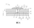
圖2A為本發明不同實施例之電子裝置的局部示意圖,而圖2B為本發明不同實施例之基板結構的示意圖。2A is a partial schematic diagram of an electronic device according to different embodiments of the invention, and FIG. 2B is a schematic diagram of a substrate structure of different embodiments of the invention.
如圖2A所示,與前述實施例之電子裝置1主要的不同在於,在本實施例的電子裝置1a中,導電件132a為一導電線,其一端E1通過所對應的通孔112電連接至導電部113,其另一端E2電連接至對應的目標導電部122。在一些實施例中,一個通孔112中可以至少容置有一條導電線(導電件132a);本實施例是以每一個通孔112容置有一條導電線(導電件132a)為例。另外,如圖2B所示的基板結構100a,黏滯層131設於載板11的第二面S2,並對應載板11的通孔112處設有穿孔h,再植入一導電線132’’。例如,黏滯層131為一黏著膠,貼附於載板11的第二面S2,此時黏滯層131的另一面仍保有離型材,於載板11的第一面S1打孔以同時形成載板11的通孔112與黏滯層131的穿孔h後,再植入導電線132”,由載板11的第一面S1對通孔112噴塗導電材15(例如錫膠),使導電線132’’於載板11的第一面S1通過導電材15連接到相應的導電部113;此時,再移除黏滯層131另一面的離型材,並對導電線132”的另一端或對目標承板12上相應的目標導電部122噴塗導電材15(例如錫膠)。之後,再將基板結構100a與目標承板12對位,進一步通過加溫,使基板結構100a的導電線132’’形成如圖2A所示的導電件132b。在一些實施例中,由黏滯層131另一面以雷射打孔,此時,黏滯層131另一面的離型材可於形成通孔112前後移除,以上說明僅為例示,本發明並不限制。As shown in FIG. 2A, the main difference from the
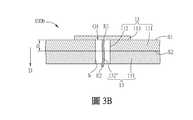
圖3A為本發明不同實施例之電子裝置的局部示意圖,而圖3B為本發明不同實施例之基板結構的示意圖。FIG. 3A is a partial schematic diagram of an electronic device according to different embodiments of the present invention, and FIG. 3B is a schematic diagram of a substrate structure according to different embodiments of the present invention.
如圖3A所示,與前述實施例之電子裝置1主要的不同在於,在本實施例的電子裝置1b中,導電件132b為一導電線,其一端E1通過所對應的通孔112電連接至導電部113,其另一端E2電連接至對應的目標導電部122。另外,如圖3B所示的基板結構100b中,導電線132”的兩端可採雷射方式電連接至相應的導電部113與目標導電部122,從而形成如圖2A所示電子裝置1b的導電件132b。在一些實施例中,載板11的第一面S1已預設有相應的導電部113,由黏滯層131另一面以雷射打孔以同時形成載板11的通孔112與黏滯層131的穿孔h, 黏滯層131另一面的離型材可於形成通孔112後移除。在一些實施例中,導電線132”植入載板11的通孔112與黏滯層131的穿孔h中,可進一步填充絕緣膠。以上說明僅為例示,本發明並不限制。As shown in FIG. 3A, the main difference from the
在一些實施例中,導電線(導電件132a、132b)可以不直接接觸通孔112的孔壁,然並不以此為限,在不同的實施例中,導電線(導電件132a、132b)也可部分接觸通孔112的孔壁。在一些實施例中,導電線(導電件132a、132b)的材料可為金屬線,例如可包括金、銅、或鋁、或其任意組合、或其任意合金。其中,導電線(導電件132a、132b)可定義有一線徑,該線徑可大於或等於0.01mm。於此,該線徑為線徑本身最大的線徑,例如可為50μm、1mil(約25μm,材料可例如為銅或金)、15μm(材料可例如為銅)、或10μm(材料可例如為金)。在一些實施例中,導電線(導電件132a、132b)的線徑可大於或等於0.005μm。可理解的是,導電線(導電件132a、132b)的線徑尚須考量可容設至通孔112的孔徑內的設計。此外,本實施例的黏滯層131的材料填滿通孔112,然並不以此為限,在不同的實施例中,黏滯層131的材料也可不填滿通孔112而留有間隙。In some embodiments, the conductive wires (
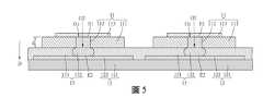
另外,圖4至圖6分別為本發明不同實施例之電子裝置的局部示意圖。In addition, FIGS. 4 to 6 are partial schematic diagrams of electronic devices according to different embodiments of the present invention.
如圖4所示,與前述實施例之電子裝置1主要的不同在於,在本實施例的電子裝置1c中,更包括多個電子元件14,該些電子元件14設在載板11的第一面S1。其中,各電子元件14包括至少一個電極141,電極141電連接至其中一個導電部113。圖4是以繪示一個電子元件14包括有兩個電極141,且兩個電極141分別與兩個導電部113接觸而電連接為例。本實施例中,兩個電極141分別通過噴塗導電材15(例如錫膠)與兩個導電部113電連接。在不同的實施例中,電子元件14的電極141也可通過導電圖層(導電層)與導電件132間接電連接,並不限制。在一些實施例中,電子元件可於載板、層結構或目標承板彼此連接後佈設;或者,電子元件可於基板結構電連接至目標承板後佈設;或者,電子元件可先佈設於本發明之基板結構上,再通過基板結構電連接至目標承板;以上說明僅為例示,本發明並不限制。可以理解的是,在一些實施例中,圖2A、圖4中繪示用以電連接的導電材15(例如錫膠)與所對應元件的電極可因共晶而構成一體。As shown in FIG. 4, the main difference from the
在一些實施例中,該些電子元件14可包括毫米級或微米級的光電晶片或光電封裝件。在一些實施例中,電子元件14可例如但不限於包括至少一發光二極體晶片(LED chip)、毫發光二極體晶片(Mini LED chip)、微發光二極體晶片(Micro LED chip)、微感測晶片(Micro sensor chip)或至少一封裝件,或不限尺寸毫米級、微米級或以下的光電晶片或光電封裝件。其中,毫米級的封裝件可包括有微米級的晶片。在一些實施例中,電子元件14可包括一個光電晶片或封裝件,而以此將電子元件14理解為單一畫素;在一些實施例中,電子元件14可包括多個光電晶片或封裝件,可以理解為電子元件14包括多個畫素。在一些實施例中,電子元件14中可包括例如紅色、藍色或綠色等LED、Mini LED、或Micro LED晶片,或其他顏色的LED、Mini LED、或Micro LED晶片或封裝件。當電子元件14包括的多個光電晶片或封裝件分別為紅色、藍色及綠色LED、Mini LED、或Micro LED晶片時,可構成全彩的LED 、Mini LED、或micro LED顯示器。圖4的電子元件14是以包括水平式電極的晶片為例,當然,在不同的實施例中,電子元件14也可以包括覆晶式電極、或垂直式電極的晶片,並以打線接合(wire bonding)或覆晶接合(flip chip bonding)與導電部113電連接。前述的封裝件不限為具有主動元件的封裝件或不具主動元件的被動封裝件,主動元件例如但不限於薄膜電晶體(TFT)或矽積體電路(Silicon IC)。在一些實施例中,電子裝置1b可進一步包括對應至少一個前述之電子元件14的一個或更多例如但不限於薄膜電晶體(TFT)或矽半導體為基礎的主動元件。在一些實施例中,電子元件14也可是一個驅動元件,該驅動元件可包含至少一薄膜電晶體(TFT)、或矽半導體為基礎的一積體電路(IC),用以驅動其他元件或封裝件。In some embodiments, the
在一些實施例中,載板11的板體111或/及目標承板12的目標板體121可分別為剛性板、軟性板、或複合板;當載板11的板體111與目標承板12的目標板體121皆為軟性板時,可使電子裝置1、1a、1b或1c成為可捲曲的軟性電子裝置,易於收納。在一些實施例中,板體111與目標板體121可為透明板或非透明板;當板體111與目標板體121分別為透明板時,可使電子裝置1、1a、1b或1c成為透明的電子產品,例如但不限於透明顯示器;載板11的板體111與目標承板12的目標板體121分別為透明且軟性板的特性,可以做到雙向透光,例如,當電子元件14包括Mini LED或Micro LED等,電子裝置1c可成為雙向透光的軟性光源或軟性顯示器。In some embodiments, the
在一些實施例中,載板11的數量可為多個,多個載板11可依據所需尺寸進行拼接,以構成大型的電子裝置,例如但不限於大型顯示器。可以理解的是,兩個相鄰載板11之間可以有間隙;或者,兩個相鄰載板11之間可以緊密連接而沒有間隙,藉此,可具有降低電子裝置1、1a、1b或1c的整體尺寸、提高元件的佈設密度、或使拼接的載板11具有視覺一致性等優點。在一些實施例中,多個載板11可拼接而排列成二維矩陣狀。本發明當其中一個載板11上的電子元件14失效時,僅須將失效的電子元件14所在的載板11汰除即可,而非汰除電子裝置的整體。In some embodiments, the number of the
另外,在多個載板11拼接的實施例中,黏滯層131的數量也可以如圖5所示為一整層,或黏滯層131的數量也可以如圖6所示是多個,使該些黏滯層131可分別對應該些載板11。換句話說,當以上述多個基板結構(包括載板11和層結構13)設置在目標承板12時,則黏滯層131的數量可對應載板11的數量與;又或者,當載板11和層結構13為各自獨立實施的元件時,則可以一個黏滯層131對應一個載板11,或一個黏滯層131對應多個載板11。在實際製程上,可以將絕緣膠或矽油以印刷或塗佈方式設在目標承板12面向層結構13的承載面S3上,例如可在目標承板12的承載面S3上按照一預定圖形一次塗佈或印刷一整層,前述的預定圖形預留有避開目標導電部122的缺口即可;或者,可按照多個預定圖形一次塗佈或印刷一整層,前述多個預定圖形可以各自獨立,且該預定圖形可對應於載板11之黏滯層131的形狀。In addition, in an embodiment where
在一些實施例中,在沿載板11的投影方向D上,載板11的投影面積與電子元件14的投影面積的比值不小於5,亦即載板11的投影面積/電子元件14的投影面積≥5。舉例來說,載板11的投影面積例如可為0.4mm*0.4mm=0.16mm2,電子元件14的投影面積例如可為(3*0.0254)mm*(5*0.0254) mm=0.0096774mm2,故載板11的投影面積/電子元件14的投影面積>16.53。舉例來說,載板11的投影面積例如可為0.8mm*0.8mm=0.64mm2,電子元件14的投影面積例如可為(5*0.0254)mm*(9*0.0254)mm =0.0290322mm2,故載板11的投影面積/電子元件14的投影面積>22.04。舉例來說,載板11的投影面積例如可為0.4mm*0.4mm=0.16mm2,電子元件14的投影面積例如可為(5*0.0254)mm*(9*0.0254)mm=0.0290322mm2,故載板11的投影面積/電子元件14的投影面積>5.51。In some embodiments, in the projection direction D along the
在一些實施例中,前述的載板11的投影面積與電子元件14的投影面積的比值可不小於50。舉例來說,載板11的投影面積例如可為0.4mm*0.4mm =0.16mm2,電子元件14的投影面積例如可為0.03mm *0.06mm =0.0018mm2,故載板11的投影面積/電子元件14的投影面積=88.88。舉例來說,載板11的投影面積例如可為0.8mm*0.8mm=0.64mm2,電子元件14的投影面積例如可為(3*0.0254)mm*(5*0.0254)mm=0.0096774mm2,故載板11的投影面積/電子元件14的投影面積>66.13。在一些實施例中,載板11的投影面積與電子元件14的投影面積的比值可不小於100。舉例來說,載板11的投影面積例如可為0.46mm*0.46mm =0.2116mm2,電子元件14的投影面積例如可為0.03mm*0.06mm=0.0018mm2,故載板11的投影面積/電子元件14的投影面積=117.56。上述的數值只是舉例,不可用以限制本發明。值得注意的是,前述的載板11的投影面積與電子元件14的投影面積,涉及面積計算通常以正方形為例,但不以正方形為限。In some embodiments, the ratio of the aforementioned projected area of the
在一些實施例中,在沿載板11的投影方向D上,電子元件14還定義其大小尺度為一元件寬度,元件寬度可不大於80mil,亦即元件寬度≤80mil。在一些實施例中,元件寬度可不大於12mil(即元件寬度≤12mil)。在一些實施例中,元件寬度可不小於0.005mm (即元件寬度≥0.005mm),例如0.008mm、0.01mm、3mil、4mil、5mil、或7mil等。In some embodiments, in the projection direction D along the
綜上所述,在本發明之基板結構與電子裝置中,透過載板的該些導電部設置於板體的第一面,且各通孔的第一開口由所對應的一個導電部所封閉;以及,層結構包括黏滯層與多個導電件,黏滯層的其中一個面與板體的第二面呈面接觸,而各導電件穿設黏滯層,並沿載板的投影方向上分別對應載板的其中一個通孔,且各導電件的一端通過所對應的通孔電連接至其中一個導電部的結構設計。藉此,由於不需在例如載板之板體另外預留導電件(或通孔)的設置空間,因此,可提高載板之導電線路(例如導電部)、及其相應的電子元件的設置密度,進而使基板結構與電子裝置可以達到較高密度的佈局設計。To sum up, in the substrate structure and electronic device of the present invention, the conductive parts through the carrier are provided on the first surface of the board, and the first opening of each through hole is closed by a corresponding conductive part And, the layer structure includes a viscous layer and a plurality of conductive members, one of the viscous layers is in surface contact with the second surface of the board, and each conductive member passes through the viscous layer and is along the projection direction of the carrier The upper part respectively corresponds to one of the through holes of the carrier, and one end of each conductive member is electrically connected to one of the conductive parts through the corresponding through hole. As a result, since there is no need to reserve additional space for the conductive elements (or through holes) in the body of the carrier, for example, the installation of the conductive circuits (for example, conductive parts) of the carrier and the corresponding electronic components can be improved. Density, so that the substrate structure and electronic devices can achieve a higher density layout design.
以上所述僅為舉例性,而非為限制性者。任何未脫離本發明之精神與範疇,而對其進行之等效修改或變更,均應包含於後附之申請專利範圍中。The above descriptions are merely illustrative and not restrictive. Any equivalent modifications or alterations that do not depart from the spirit and scope of the present invention should be included in the scope of the appended patent application.
1,1a,1b,1c:電子裝置 100,100a,100b:基板結構 11:載板 111:板體 112:通孔 113:導電部 12:目標承板 121:目標板體 122:目標導電部 13:層結構 131:黏滯層 132,132a,132b:導電件 132’:錫球 132”:導電線 14:電子元件 141:電極 15:導電材 d:厚度 D:投影方向 E1,E2:端 h:穿孔 O1:第一開口 O2:第二開口 S1:第一面 S2:第二面 S3:承載面1,1a,1b,1c:
圖1A為本發明一實施例之電子裝置的局部示意圖。 圖1B為本發明一實施例之基板結構的示意圖。 圖2A為本發明不同實施例之電子裝置的局部示意圖。 圖2B為本發明不同實施例之基板結構的示意圖。 圖3A為本發明不同實施例之電子裝置的局部示意圖。 圖3B為本發明不同實施例之基板結構的示意圖。 圖4至圖6分別為本發明不同實施例之電子裝置的局部示意圖。FIG. 1A is a partial schematic diagram of an electronic device according to an embodiment of the invention. FIG. 1B is a schematic diagram of a substrate structure according to an embodiment of the invention. 2A is a partial schematic diagram of an electronic device according to different embodiments of the invention. FIG. 2B is a schematic diagram of a substrate structure according to different embodiments of the present invention. FIG. 3A is a partial schematic diagram of an electronic device according to different embodiments of the present invention. FIG. 3B is a schematic diagram of the substrate structure of different embodiments of the present invention. 4 to 6 are partial schematic diagrams of electronic devices according to different embodiments of the present invention.
1:電子裝置1: Electronic device
11:載板11: Carrier board
111:板體111: Board body
112:通孔112: Through hole
113:導電部113: Conductive part
12:目標承板12: Target bearing plate
121:目標板體121: target board body
122:目標導電部122: target conductive part
13:層結構13: layer structure
131:黏滯層131: Viscous Layer
132:導電件132: Conductive parts
d:厚度d: thickness
D:投影方向D: Projection direction
E1,E2:端E1, E2: end
O1:第一開口O1: first opening
O2:第二開口O2: second opening
S1:第一面S1: First side
S2:第二面S2: Second side
S3:承載面S3: bearing surface
Claims (28)
Translated fromChinesePriority Applications (2)
| Application Number | Priority Date | Filing Date | Title |
|---|---|---|---|
| TW110102209ATWI742991B (en) | 2021-01-20 | 2021-01-20 | Substrate structure and electronic device |
| US17/555,727US12278314B2 (en) | 2021-01-20 | 2021-12-20 | Substrate structure with high density layout and electronic device using the same |
Applications Claiming Priority (1)
| Application Number | Priority Date | Filing Date | Title |
|---|---|---|---|
| TW110102209ATWI742991B (en) | 2021-01-20 | 2021-01-20 | Substrate structure and electronic device |
Publications (2)
| Publication Number | Publication Date |
|---|---|
| TWI742991Btrue TWI742991B (en) | 2021-10-11 |
| TW202230639A TW202230639A (en) | 2022-08-01 |
Family
ID=80782640
Family Applications (1)
| Application Number | Title | Priority Date | Filing Date |
|---|---|---|---|
| TW110102209ATWI742991B (en) | 2021-01-20 | 2021-01-20 | Substrate structure and electronic device |
Country Status (2)
| Country | Link |
|---|---|
| US (1) | US12278314B2 (en) |
| TW (1) | TWI742991B (en) |
Families Citing this family (3)
| Publication number | Priority date | Publication date | Assignee | Title |
|---|---|---|---|---|
| TWI742991B (en)* | 2021-01-20 | 2021-10-11 | 啟耀光電股份有限公司 | Substrate structure and electronic device |
| JP2023043862A (en)* | 2021-09-16 | 2023-03-29 | 方略電子股▲ふん▼有限公司 | electronic device |
| WO2024031563A1 (en)* | 2022-08-11 | 2024-02-15 | 京东方科技集团股份有限公司 | Display panel, display device and tiled display device |
Citations (6)
| Publication number | Priority date | Publication date | Assignee | Title |
|---|---|---|---|---|
| US20080224271A1 (en)* | 2004-12-27 | 2008-09-18 | Nec Corporation | Semiconductor Device and Method of Manufacturing Same, Wiring Board and Method of Manufacturing Same, Semiconductor Package, and Electronic Device |
| TW201916305A (en)* | 2017-09-18 | 2019-04-16 | 台灣積體電路製造股份有限公司 | Package structure |
| TW201917853A (en)* | 2017-10-24 | 2019-05-01 | 啟耀光電股份有限公司 | Electronic device and manufacturing method thereof |
| TW201926550A (en)* | 2017-11-30 | 2019-07-01 | 台灣積體電路製造股份有限公司 | Semiconductor device manufacturing method and structure |
| TW201929215A (en)* | 2017-12-22 | 2019-07-16 | 啟耀光電股份有限公司 | Electronic package unit and manufacturing method thereof and electronic device |
| TW202038426A (en)* | 2015-01-13 | 2020-10-16 | 日商迪睿合股份有限公司 | Multilayer substrate, connection structure and connection structure manufacturing method |
Family Cites Families (51)
| Publication number | Priority date | Publication date | Assignee | Title |
|---|---|---|---|---|
| US3077511A (en)* | 1960-03-11 | 1963-02-12 | Int Resistance Co | Printed circuit unit |
| DE1933731C3 (en)* | 1968-07-05 | 1982-03-25 | Honeywell Information Systems Italia S.p.A., Caluso, Torino | Method for producing a semiconductor integrated circuit |
| JP2753746B2 (en)* | 1989-11-06 | 1998-05-20 | 日本メクトロン株式会社 | Flexible circuit board for mounting IC and method of manufacturing the same |
| US5203075A (en)* | 1991-08-12 | 1993-04-20 | Inernational Business Machines | Method of bonding flexible circuit to cicuitized substrate to provide electrical connection therebetween using different solders |
| US5873161A (en)* | 1996-07-23 | 1999-02-23 | Minnesota Mining And Manufacturing Company | Method of making a Z axis interconnect circuit |
| US6225569B1 (en)* | 1996-11-15 | 2001-05-01 | Ngk Spark Plug Co., Ltd. | Wiring substrate and method of manufacturing the same |
| JP3732923B2 (en)* | 1997-06-25 | 2006-01-11 | 京セラ株式会社 | Wiring board |
| JP3250216B2 (en)* | 1998-08-13 | 2002-01-28 | ソニーケミカル株式会社 | Flexible printed wiring board and method of manufacturing the same |
| US6400018B2 (en)* | 1998-08-27 | 2002-06-04 | 3M Innovative Properties Company | Via plug adapter |
| JP3205548B2 (en)* | 1999-10-01 | 2001-09-04 | ソニーケミカル株式会社 | Multi-layer flexible wiring board |
| DE60034937T2 (en)* | 2000-01-25 | 2008-02-14 | Sony Chemical & Information Device Corp. | FLEXIBLE PRINTED PCB AND ITS MANUFACTURING METHOD |
| US6800815B1 (en)* | 2001-01-16 | 2004-10-05 | National Semiconductor Corporation | Materials and structure for a high reliability bga connection between LTCC and PB boards |
| JP4181510B2 (en)* | 2003-02-28 | 2008-11-19 | 日本特殊陶業株式会社 | Resin wiring board |
| US20060289203A1 (en)* | 2003-05-19 | 2006-12-28 | Dai Nippon Printing Co., Ltd. | Double-sided wiring board, double sided wiring board manufacturing method, and multilayer wiring board |
| US20050001309A1 (en)* | 2003-06-20 | 2005-01-06 | Akinori Tanaka | Printed wiring board for mounting semiconductor |
| JPWO2006064863A1 (en)* | 2004-12-17 | 2008-06-12 | イビデン株式会社 | Printed wiring board |
| TWI288447B (en)* | 2005-04-12 | 2007-10-11 | Siliconware Precision Industries Co Ltd | Conductive bump structure for semiconductor device and fabrication method thereof |
| US7550319B2 (en)* | 2005-09-01 | 2009-06-23 | E. I. Du Pont De Nemours And Company | Low temperature co-fired ceramic (LTCC) tape compositions, light emitting diode (LED) modules, lighting devices and method of forming thereof |
| US20080142252A1 (en)* | 2006-12-13 | 2008-06-19 | Romi Mayder | Solid via with a contact pad for mating with an interposer of an ATE tester |
| JP5324051B2 (en)* | 2007-03-29 | 2013-10-23 | 新光電気工業株式会社 | Wiring substrate manufacturing method, semiconductor device manufacturing method, and wiring substrate |
| JP5032187B2 (en)* | 2007-04-17 | 2012-09-26 | 新光電気工業株式会社 | Wiring substrate manufacturing method, semiconductor device manufacturing method, and wiring substrate |
| JP2009135147A (en)* | 2007-11-28 | 2009-06-18 | Shinko Electric Ind Co Ltd | Connection structure of wiring board and electronic element, and electronic device |
| JP4803844B2 (en)* | 2008-10-21 | 2011-10-26 | インターナショナル・ビジネス・マシーンズ・コーポレーション | Semiconductor package |
| JP5269563B2 (en)* | 2008-11-28 | 2013-08-21 | 新光電気工業株式会社 | Wiring board and manufacturing method thereof |
| US9627254B2 (en)* | 2009-07-02 | 2017-04-18 | Flipchip International, Llc | Method for building vertical pillar interconnect |
| KR101645771B1 (en)* | 2010-05-12 | 2016-08-04 | 르네사스 일렉트로닉스 가부시키가이샤 | Semiconductor device and method for manufacturing same |
| US8487445B1 (en)* | 2010-10-05 | 2013-07-16 | Amkor Technology, Inc. | Semiconductor device having through electrodes protruding from dielectric layer |
| US8354684B2 (en)* | 2011-01-09 | 2013-01-15 | Bridgelux, Inc. | Packaging photon building blocks having only top side connections in an interconnect structure |
| JP5886617B2 (en)* | 2011-12-02 | 2016-03-16 | 新光電気工業株式会社 | Wiring substrate, manufacturing method thereof, and semiconductor package |
| KR101332049B1 (en)* | 2012-01-13 | 2013-11-22 | 삼성전기주식회사 | Method for manufacturing Printed circuit board |
| JP5868274B2 (en)* | 2012-06-29 | 2016-02-24 | 京セラサーキットソリューションズ株式会社 | WIRING BOARD AND ELECTRONIC DEVICE USING THE SAME |
| KR101506785B1 (en)* | 2013-05-29 | 2015-03-27 | 삼성전기주식회사 | Printed Circuit Board |
| JP6657609B2 (en)* | 2015-06-12 | 2020-03-04 | 凸版印刷株式会社 | Wiring circuit board, semiconductor device, method of manufacturing wiring circuit board, and method of manufacturing semiconductor device |
| WO2017007200A2 (en)* | 2015-07-03 | 2017-01-12 | 주식회사 오킨스전자 | Test socket, test socket manufacturing method, and jig assembly for test socket |
| WO2019044706A1 (en)* | 2017-08-29 | 2019-03-07 | 京セラ株式会社 | Substrate for mounting electronic components, electronic device, and electronic module |
| TWI693449B (en)* | 2018-10-18 | 2020-05-11 | 啟耀光電股份有限公司 | Electronic device and manufacturing method thereof |
| TWI838548B (en)* | 2020-06-24 | 2024-04-11 | 方略電子股份有限公司 | Light-emitting device |
| CN114080100B (en)* | 2020-08-21 | 2024-11-12 | 欣兴电子股份有限公司 | Circuit board and method for forming holes therein |
| CN114695304A (en)* | 2020-12-28 | 2022-07-01 | 华雅应用材料股份有限公司 | Substrate structure and electronic device |
| TWI845799B (en)* | 2020-12-28 | 2024-06-21 | 方略電子股份有限公司 | Substrate structure and electronic device |
| US11678438B2 (en)* | 2020-12-30 | 2023-06-13 | Panelsemi Corporation | Electronic device |
| TWI742991B (en)* | 2021-01-20 | 2021-10-11 | 啟耀光電股份有限公司 | Substrate structure and electronic device |
| US20220359213A1 (en)* | 2021-05-04 | 2022-11-10 | Panelsemi Corporation | Method for fabricating semiconductor chip structures, semiconductor carrier and semiconductor chip structure |
| JP2023043862A (en)* | 2021-09-16 | 2023-03-29 | 方略電子股▲ふん▼有限公司 | electronic device |
| US20230187333A1 (en)* | 2021-12-13 | 2023-06-15 | Panelsemi Corporation | Substrate structure and electronic device |
| US12230892B2 (en)* | 2021-12-22 | 2025-02-18 | Panelsemi Corporation | Electronic device |
| TW202341396A (en)* | 2022-04-01 | 2023-10-16 | 方略電子股份有限公司 | Electronic device and antenna device |
| TW202401898A (en)* | 2022-06-24 | 2024-01-01 | 方略電子股份有限公司 | Antenna device |
| US12389537B2 (en)* | 2022-09-08 | 2025-08-12 | Panelsemi Corporation | Electronic device |
| US20240090129A1 (en)* | 2022-09-08 | 2024-03-14 | Panelsemi Corporation | Electronic device |
| TW202418899A (en)* | 2022-10-28 | 2024-05-01 | 方略電子股份有限公司 | Electronic device and electronic apparatus |
- 2021
- 2021-01-20TWTW110102209Apatent/TWI742991B/enactive
- 2021-12-20USUS17/555,727patent/US12278314B2/enactiveActive
Patent Citations (6)
| Publication number | Priority date | Publication date | Assignee | Title |
|---|---|---|---|---|
| US20080224271A1 (en)* | 2004-12-27 | 2008-09-18 | Nec Corporation | Semiconductor Device and Method of Manufacturing Same, Wiring Board and Method of Manufacturing Same, Semiconductor Package, and Electronic Device |
| TW202038426A (en)* | 2015-01-13 | 2020-10-16 | 日商迪睿合股份有限公司 | Multilayer substrate, connection structure and connection structure manufacturing method |
| TW201916305A (en)* | 2017-09-18 | 2019-04-16 | 台灣積體電路製造股份有限公司 | Package structure |
| TW201917853A (en)* | 2017-10-24 | 2019-05-01 | 啟耀光電股份有限公司 | Electronic device and manufacturing method thereof |
| TW201926550A (en)* | 2017-11-30 | 2019-07-01 | 台灣積體電路製造股份有限公司 | Semiconductor device manufacturing method and structure |
| TW201929215A (en)* | 2017-12-22 | 2019-07-16 | 啟耀光電股份有限公司 | Electronic package unit and manufacturing method thereof and electronic device |
Also Published As
| Publication number | Publication date |
|---|---|
| TW202230639A (en) | 2022-08-01 |
| US20220231198A1 (en) | 2022-07-21 |
| US12278314B2 (en) | 2025-04-15 |
Similar Documents
| Publication | Publication Date | Title |
|---|---|---|
| US11411152B2 (en) | Packaging photon building blocks with top side connections and interconnect structure | |
| CN112599510B (en) | Miniature LED display matrix module | |
| TWI742991B (en) | Substrate structure and electronic device | |
| KR102322539B1 (en) | Semiconductor package and display apparatus comprising the same | |
| US11127341B2 (en) | Light emitting module and display device | |
| JP3565334B2 (en) | Semiconductor device, liquid crystal module using the same, and method of manufacturing semiconductor device | |
| JP2008135694A (en) | LED module | |
| JP2004343030A (en) | Wiring circuit board, manufacturing method thereof, circuit module provided with this wiring circuit board | |
| CN100559583C (en) | LED components | |
| CN112913026A (en) | Mounting Structure for Mounting Micro LEDs | |
| CN109216525B (en) | Light emitting module and display device | |
| TW202226392A (en) | Substrate structure and manufacturing method thereof, electronic device | |
| JP6600353B2 (en) | Printed circuit board and printed circuit board layout | |
| TW201933580A (en) | Conductive film, optoelectronic semiconductor device and manufacturing method of the same | |
| JP6957599B2 (en) | Luminescent device and its manufacturing method | |
| CN114072928B (en) | LED module and display device comprising same | |
| CN100416343C (en) | Structure for increasing reliability of metal connection | |
| KR20090044483A (en) | Semiconductor package | |
| CN114864798A (en) | Substrate structures and electronic devices | |
| CN114695304A (en) | Substrate structure and electronic device | |
| CN100433320C (en) | Chip packaging structure and bump manufacturing process | |
| TW202322327A (en) | Chip packaging structure and manufacturing method thereof | |
| CN101625986A (en) | Chip packaging structure manufacturing process | |
| TWI882286B (en) | Small pitch light emitting module and conductive substrate thereof | |
| TWI812124B (en) | Electronic module and carrier structure thereof and manufacturing method thereof |