TWI742256B - Direct-bonded led arrays and applications - Google Patents
Direct-bonded led arrays and applicationsDownload PDFInfo
- Publication number
- TWI742256B TWI742256BTW107108645ATW107108645ATWI742256BTW I742256 BTWI742256 BTW I742256BTW 107108645 ATW107108645 ATW 107108645ATW 107108645 ATW107108645 ATW 107108645ATW I742256 BTWI742256 BTW I742256B
- Authority
- TW
- Taiwan
- Prior art keywords
- wafer
- led
- coplanar
- bonding surface
- contact point
- Prior art date
Links
Images


Classifications
- H—ELECTRICITY
- H01—ELECTRIC ELEMENTS
- H01L—SEMICONDUCTOR DEVICES NOT COVERED BY CLASS H10
- H01L25/00—Assemblies consisting of a plurality of semiconductor or other solid state devices
- H01L25/16—Assemblies consisting of a plurality of semiconductor or other solid state devices the devices being of types provided for in two or more different subclasses of H10B, H10D, H10F, H10H, H10K or H10N, e.g. forming hybrid circuits
- H01L25/167—Assemblies consisting of a plurality of semiconductor or other solid state devices the devices being of types provided for in two or more different subclasses of H10B, H10D, H10F, H10H, H10K or H10N, e.g. forming hybrid circuits comprising optoelectronic devices, e.g. LED, photodiodes
- H—ELECTRICITY
- H01—ELECTRIC ELEMENTS
- H01L—SEMICONDUCTOR DEVICES NOT COVERED BY CLASS H10
- H01L21/00—Processes or apparatus adapted for the manufacture or treatment of semiconductor or solid state devices or of parts thereof
- H01L21/02—Manufacture or treatment of semiconductor devices or of parts thereof
- H01L21/02104—Forming layers
- H01L21/02107—Forming insulating materials on a substrate
- H01L21/02109—Forming insulating materials on a substrate characterised by the type of layer, e.g. type of material, porous/non-porous, pre-cursors, mixtures or laminates
- H01L21/02112—Forming insulating materials on a substrate characterised by the type of layer, e.g. type of material, porous/non-porous, pre-cursors, mixtures or laminates characterised by the material of the layer
- H01L21/02118—Forming insulating materials on a substrate characterised by the type of layer, e.g. type of material, porous/non-porous, pre-cursors, mixtures or laminates characterised by the material of the layer carbon based polymeric organic or inorganic material, e.g. polyimides, poly cyclobutene or PVC
- H—ELECTRICITY
- H01—ELECTRIC ELEMENTS
- H01L—SEMICONDUCTOR DEVICES NOT COVERED BY CLASS H10
- H01L21/00—Processes or apparatus adapted for the manufacture or treatment of semiconductor or solid state devices or of parts thereof
- H01L21/02—Manufacture or treatment of semiconductor devices or of parts thereof
- H01L21/04—Manufacture or treatment of semiconductor devices or of parts thereof the devices having potential barriers, e.g. a PN junction, depletion layer or carrier concentration layer
- H01L21/18—Manufacture or treatment of semiconductor devices or of parts thereof the devices having potential barriers, e.g. a PN junction, depletion layer or carrier concentration layer the devices having semiconductor bodies comprising elements of Group IV of the Periodic Table or AIIIBV compounds with or without impurities, e.g. doping materials
- H01L21/30—Treatment of semiconductor bodies using processes or apparatus not provided for in groups H01L21/20 - H01L21/26
- H01L21/31—Treatment of semiconductor bodies using processes or apparatus not provided for in groups H01L21/20 - H01L21/26 to form insulating layers thereon, e.g. for masking or by using photolithographic techniques; After treatment of these layers; Selection of materials for these layers
- H01L21/3205—Deposition of non-insulating-, e.g. conductive- or resistive-, layers on insulating layers; After-treatment of these layers
- H01L21/321—After treatment
- H01L21/32115—Planarisation
- H01L21/3212—Planarisation by chemical mechanical polishing [CMP]
- H—ELECTRICITY
- H01—ELECTRIC ELEMENTS
- H01L—SEMICONDUCTOR DEVICES NOT COVERED BY CLASS H10
- H01L24/00—Arrangements for connecting or disconnecting semiconductor or solid-state bodies; Methods or apparatus related thereto
- H01L24/01—Means for bonding being attached to, or being formed on, the surface to be connected, e.g. chip-to-package, die-attach, "first-level" interconnects; Manufacturing methods related thereto
- H01L24/02—Bonding areas ; Manufacturing methods related thereto
- H01L24/07—Structure, shape, material or disposition of the bonding areas after the connecting process
- H01L24/08—Structure, shape, material or disposition of the bonding areas after the connecting process of an individual bonding area
- H—ELECTRICITY
- H01—ELECTRIC ELEMENTS
- H01L—SEMICONDUCTOR DEVICES NOT COVERED BY CLASS H10
- H01L24/00—Arrangements for connecting or disconnecting semiconductor or solid-state bodies; Methods or apparatus related thereto
- H01L24/80—Methods for connecting semiconductor or other solid state bodies using means for bonding being attached to, or being formed on, the surface to be connected
- H—ELECTRICITY
- H01—ELECTRIC ELEMENTS
- H01L—SEMICONDUCTOR DEVICES NOT COVERED BY CLASS H10
- H01L25/00—Assemblies consisting of a plurality of semiconductor or other solid state devices
- H01L25/03—Assemblies consisting of a plurality of semiconductor or other solid state devices all the devices being of a type provided for in a single subclass of subclasses H10B, H10D, H10F, H10H, H10K or H10N, e.g. assemblies of rectifier diodes
- H01L25/10—Assemblies consisting of a plurality of semiconductor or other solid state devices all the devices being of a type provided for in a single subclass of subclasses H10B, H10D, H10F, H10H, H10K or H10N, e.g. assemblies of rectifier diodes the devices having separate containers
- H01L25/105—Assemblies consisting of a plurality of semiconductor or other solid state devices all the devices being of a type provided for in a single subclass of subclasses H10B, H10D, H10F, H10H, H10K or H10N, e.g. assemblies of rectifier diodes the devices having separate containers the devices being integrated devices of class H10
- H—ELECTRICITY
- H01—ELECTRIC ELEMENTS
- H01L—SEMICONDUCTOR DEVICES NOT COVERED BY CLASS H10
- H01L25/00—Assemblies consisting of a plurality of semiconductor or other solid state devices
- H01L25/18—Assemblies consisting of a plurality of semiconductor or other solid state devices the devices being of the types provided for in two or more different main groups of the same subclass of H10B, H10D, H10F, H10H, H10K or H10N
- H—ELECTRICITY
- H10—SEMICONDUCTOR DEVICES; ELECTRIC SOLID-STATE DEVICES NOT OTHERWISE PROVIDED FOR
- H10D—INORGANIC ELECTRIC SEMICONDUCTOR DEVICES
- H10D86/00—Integrated devices formed in or on insulating or conducting substrates, e.g. formed in silicon-on-insulator [SOI] substrates or on stainless steel or glass substrates
- H10D86/40—Integrated devices formed in or on insulating or conducting substrates, e.g. formed in silicon-on-insulator [SOI] substrates or on stainless steel or glass substrates characterised by multiple TFTs
- H10D86/60—Integrated devices formed in or on insulating or conducting substrates, e.g. formed in silicon-on-insulator [SOI] substrates or on stainless steel or glass substrates characterised by multiple TFTs wherein the TFTs are in active matrices
- H—ELECTRICITY
- H10—SEMICONDUCTOR DEVICES; ELECTRIC SOLID-STATE DEVICES NOT OTHERWISE PROVIDED FOR
- H10H—INORGANIC LIGHT-EMITTING SEMICONDUCTOR DEVICES HAVING POTENTIAL BARRIERS
- H10H20/00—Individual inorganic light-emitting semiconductor devices having potential barriers, e.g. light-emitting diodes [LED]
- H10H20/01—Manufacture or treatment
- H10H20/011—Manufacture or treatment of bodies, e.g. forming semiconductor layers
- H10H20/013—Manufacture or treatment of bodies, e.g. forming semiconductor layers having light-emitting regions comprising only Group III-V materials
- H10H20/0133—Manufacture or treatment of bodies, e.g. forming semiconductor layers having light-emitting regions comprising only Group III-V materials with a substrate not being Group III-V materials
- H10H20/01335—Manufacture or treatment of bodies, e.g. forming semiconductor layers having light-emitting regions comprising only Group III-V materials with a substrate not being Group III-V materials the light-emitting regions comprising nitride materials
- H—ELECTRICITY
- H10—SEMICONDUCTOR DEVICES; ELECTRIC SOLID-STATE DEVICES NOT OTHERWISE PROVIDED FOR
- H10H—INORGANIC LIGHT-EMITTING SEMICONDUCTOR DEVICES HAVING POTENTIAL BARRIERS
- H10H20/00—Individual inorganic light-emitting semiconductor devices having potential barriers, e.g. light-emitting diodes [LED]
- H10H20/01—Manufacture or treatment
- H10H20/011—Manufacture or treatment of bodies, e.g. forming semiconductor layers
- H10H20/018—Bonding of wafers
- H—ELECTRICITY
- H10—SEMICONDUCTOR DEVICES; ELECTRIC SOLID-STATE DEVICES NOT OTHERWISE PROVIDED FOR
- H10H—INORGANIC LIGHT-EMITTING SEMICONDUCTOR DEVICES HAVING POTENTIAL BARRIERS
- H10H29/00—Integrated devices, or assemblies of multiple devices, comprising at least one light-emitting semiconductor element covered by group H10H20/00
- H10H29/10—Integrated devices comprising at least one light-emitting semiconductor component covered by group H10H20/00
- H10H29/14—Integrated devices comprising at least one light-emitting semiconductor component covered by group H10H20/00 comprising multiple light-emitting semiconductor components
- H10H29/142—Two-dimensional arrangements, e.g. asymmetric LED layout
- H—ELECTRICITY
- H01—ELECTRIC ELEMENTS
- H01L—SEMICONDUCTOR DEVICES NOT COVERED BY CLASS H10
- H01L2224/00—Indexing scheme for arrangements for connecting or disconnecting semiconductor or solid-state bodies and methods related thereto as covered by H01L24/00
- H01L2224/01—Means for bonding being attached to, or being formed on, the surface to be connected, e.g. chip-to-package, die-attach, "first-level" interconnects; Manufacturing methods related thereto
- H01L2224/02—Bonding areas; Manufacturing methods related thereto
- H01L2224/07—Structure, shape, material or disposition of the bonding areas after the connecting process
- H01L2224/08—Structure, shape, material or disposition of the bonding areas after the connecting process of an individual bonding area
- H01L2224/081—Disposition
- H01L2224/0812—Disposition the bonding area connecting directly to another bonding area, i.e. connectorless bonding, e.g. bumpless bonding
- H01L2224/08135—Disposition the bonding area connecting directly to another bonding area, i.e. connectorless bonding, e.g. bumpless bonding the bonding area connecting between different semiconductor or solid-state bodies, i.e. chip-to-chip
- H01L2224/08137—Disposition the bonding area connecting directly to another bonding area, i.e. connectorless bonding, e.g. bumpless bonding the bonding area connecting between different semiconductor or solid-state bodies, i.e. chip-to-chip the bodies being arranged next to each other, e.g. on a common substrate
- H—ELECTRICITY
- H01—ELECTRIC ELEMENTS
- H01L—SEMICONDUCTOR DEVICES NOT COVERED BY CLASS H10
- H01L2224/00—Indexing scheme for arrangements for connecting or disconnecting semiconductor or solid-state bodies and methods related thereto as covered by H01L24/00
- H01L2224/01—Means for bonding being attached to, or being formed on, the surface to be connected, e.g. chip-to-package, die-attach, "first-level" interconnects; Manufacturing methods related thereto
- H01L2224/02—Bonding areas; Manufacturing methods related thereto
- H01L2224/07—Structure, shape, material or disposition of the bonding areas after the connecting process
- H01L2224/08—Structure, shape, material or disposition of the bonding areas after the connecting process of an individual bonding area
- H01L2224/081—Disposition
- H01L2224/0812—Disposition the bonding area connecting directly to another bonding area, i.e. connectorless bonding, e.g. bumpless bonding
- H01L2224/08135—Disposition the bonding area connecting directly to another bonding area, i.e. connectorless bonding, e.g. bumpless bonding the bonding area connecting between different semiconductor or solid-state bodies, i.e. chip-to-chip
- H01L2224/08145—Disposition the bonding area connecting directly to another bonding area, i.e. connectorless bonding, e.g. bumpless bonding the bonding area connecting between different semiconductor or solid-state bodies, i.e. chip-to-chip the bodies being stacked
- H—ELECTRICITY
- H01—ELECTRIC ELEMENTS
- H01L—SEMICONDUCTOR DEVICES NOT COVERED BY CLASS H10
- H01L2224/00—Indexing scheme for arrangements for connecting or disconnecting semiconductor or solid-state bodies and methods related thereto as covered by H01L24/00
- H01L2224/80—Methods for connecting semiconductor or other solid state bodies using means for bonding being attached to, or being formed on, the surface to be connected
- H01L2224/80001—Methods for connecting semiconductor or other solid state bodies using means for bonding being attached to, or being formed on, the surface to be connected by connecting a bonding area directly to another bonding area, i.e. connectorless bonding, e.g. bumpless bonding
- H01L2224/80009—Pre-treatment of the bonding area
- H01L2224/8001—Cleaning the bonding area, e.g. oxide removal step, desmearing
- H01L2224/80013—Plasma cleaning
- H—ELECTRICITY
- H01—ELECTRIC ELEMENTS
- H01L—SEMICONDUCTOR DEVICES NOT COVERED BY CLASS H10
- H01L2224/00—Indexing scheme for arrangements for connecting or disconnecting semiconductor or solid-state bodies and methods related thereto as covered by H01L24/00
- H01L2224/80—Methods for connecting semiconductor or other solid state bodies using means for bonding being attached to, or being formed on, the surface to be connected
- H01L2224/80001—Methods for connecting semiconductor or other solid state bodies using means for bonding being attached to, or being formed on, the surface to be connected by connecting a bonding area directly to another bonding area, i.e. connectorless bonding, e.g. bumpless bonding
- H01L2224/8034—Bonding interfaces of the bonding area
- H01L2224/80355—Bonding interfaces of the bonding area having an external coating, e.g. protective bond-through coating
- H—ELECTRICITY
- H01—ELECTRIC ELEMENTS
- H01L—SEMICONDUCTOR DEVICES NOT COVERED BY CLASS H10
- H01L2224/00—Indexing scheme for arrangements for connecting or disconnecting semiconductor or solid-state bodies and methods related thereto as covered by H01L24/00
- H01L2224/80—Methods for connecting semiconductor or other solid state bodies using means for bonding being attached to, or being formed on, the surface to be connected
- H01L2224/80001—Methods for connecting semiconductor or other solid state bodies using means for bonding being attached to, or being formed on, the surface to be connected by connecting a bonding area directly to another bonding area, i.e. connectorless bonding, e.g. bumpless bonding
- H01L2224/8034—Bonding interfaces of the bonding area
- H01L2224/80357—Bonding interfaces of the bonding area being flush with the surface
- H—ELECTRICITY
- H10—SEMICONDUCTOR DEVICES; ELECTRIC SOLID-STATE DEVICES NOT OTHERWISE PROVIDED FOR
- H10H—INORGANIC LIGHT-EMITTING SEMICONDUCTOR DEVICES HAVING POTENTIAL BARRIERS
- H10H20/00—Individual inorganic light-emitting semiconductor devices having potential barriers, e.g. light-emitting diodes [LED]
- H10H20/01—Manufacture or treatment
- H10H20/032—Manufacture or treatment of electrodes
- H—ELECTRICITY
- H10—SEMICONDUCTOR DEVICES; ELECTRIC SOLID-STATE DEVICES NOT OTHERWISE PROVIDED FOR
- H10H—INORGANIC LIGHT-EMITTING SEMICONDUCTOR DEVICES HAVING POTENTIAL BARRIERS
- H10H20/00—Individual inorganic light-emitting semiconductor devices having potential barriers, e.g. light-emitting diodes [LED]
- H10H20/01—Manufacture or treatment
- H10H20/034—Manufacture or treatment of coatings
- H—ELECTRICITY
- H10—SEMICONDUCTOR DEVICES; ELECTRIC SOLID-STATE DEVICES NOT OTHERWISE PROVIDED FOR
- H10H—INORGANIC LIGHT-EMITTING SEMICONDUCTOR DEVICES HAVING POTENTIAL BARRIERS
- H10H20/00—Individual inorganic light-emitting semiconductor devices having potential barriers, e.g. light-emitting diodes [LED]
- H10H20/01—Manufacture or treatment
- H10H20/036—Manufacture or treatment of packages
- H10H20/0364—Manufacture or treatment of packages of interconnections
- H—ELECTRICITY
- H10—SEMICONDUCTOR DEVICES; ELECTRIC SOLID-STATE DEVICES NOT OTHERWISE PROVIDED FOR
- H10H—INORGANIC LIGHT-EMITTING SEMICONDUCTOR DEVICES HAVING POTENTIAL BARRIERS
- H10H20/00—Individual inorganic light-emitting semiconductor devices having potential barriers, e.g. light-emitting diodes [LED]
- H10H20/80—Constructional details
- H10H20/81—Bodies
- H10H20/811—Bodies having quantum effect structures or superlattices, e.g. tunnel junctions
- H10H20/812—Bodies having quantum effect structures or superlattices, e.g. tunnel junctions within the light-emitting regions, e.g. having quantum confinement structures
- H—ELECTRICITY
- H10—SEMICONDUCTOR DEVICES; ELECTRIC SOLID-STATE DEVICES NOT OTHERWISE PROVIDED FOR
- H10H—INORGANIC LIGHT-EMITTING SEMICONDUCTOR DEVICES HAVING POTENTIAL BARRIERS
- H10H20/00—Individual inorganic light-emitting semiconductor devices having potential barriers, e.g. light-emitting diodes [LED]
- H10H20/80—Constructional details
- H10H20/81—Bodies
- H10H20/822—Materials of the light-emitting regions
- H10H20/824—Materials of the light-emitting regions comprising only Group III-V materials, e.g. GaP
- H10H20/825—Materials of the light-emitting regions comprising only Group III-V materials, e.g. GaP containing nitrogen, e.g. GaN
- H—ELECTRICITY
- H10—SEMICONDUCTOR DEVICES; ELECTRIC SOLID-STATE DEVICES NOT OTHERWISE PROVIDED FOR
- H10H—INORGANIC LIGHT-EMITTING SEMICONDUCTOR DEVICES HAVING POTENTIAL BARRIERS
- H10H20/00—Individual inorganic light-emitting semiconductor devices having potential barriers, e.g. light-emitting diodes [LED]
- H10H20/80—Constructional details
- H10H20/84—Coatings, e.g. passivation layers or antireflective coatings
- H10H20/841—Reflective coatings, e.g. dielectric Bragg reflectors
- H—ELECTRICITY
- H10—SEMICONDUCTOR DEVICES; ELECTRIC SOLID-STATE DEVICES NOT OTHERWISE PROVIDED FOR
- H10H—INORGANIC LIGHT-EMITTING SEMICONDUCTOR DEVICES HAVING POTENTIAL BARRIERS
- H10H20/00—Individual inorganic light-emitting semiconductor devices having potential barriers, e.g. light-emitting diodes [LED]
- H10H20/80—Constructional details
- H10H20/85—Packages
- H10H20/857—Interconnections, e.g. lead-frames, bond wires or solder balls
Landscapes
- Engineering & Computer Science (AREA)
- Microelectronics & Electronic Packaging (AREA)
- Power Engineering (AREA)
- Computer Hardware Design (AREA)
- Physics & Mathematics (AREA)
- Condensed Matter Physics & Semiconductors (AREA)
- General Physics & Mathematics (AREA)
- Manufacturing & Machinery (AREA)
- Led Devices (AREA)
- Led Device Packages (AREA)
Abstract
Description
Translated fromChinese本發明關於一種直接接合的LED陣列及應用。The invention relates to a directly bonded LED array and its application.
本專利申請案主張Tao等人於2017年3月16日申請之標題為「直接接合的LED陣列及應用(Direct Bonded LED Arrays and Applications)」的第62/472,363號美國臨時專利申請案之優先權益,且該申請案以全文引用之方式併入本文中。This patent application claims the priority of the U.S. Provisional Patent Application No. 62/472,363 entitled "Direct Bonded LED Arrays and Applications" filed on March 16, 2017 by Tao et al. , And the application is incorporated herein by reference in its entirety.
如本文中所使用,亦稱為微LED(micro-LED)、pLED及「mLED」之微LED(MicroLED)正作為一種新興之平板顯示技術而獲得顯著吸引力。但迄今為止,mLED顯示器尚未廣泛地量產或商品化。mLED顯示器為形成獨立像素元件之微觀LED的陣列。與廣泛之LCD技術相比較,mLED顯示器提供較大對比度及較快回應時間,同時使用較少能量。As used in this article, also known as micro-LED (micro-LED), pLED and "mLED" micro LED (MicroLED) is gaining significant appeal as an emerging flat panel display technology. But so far, mLED displays have not been widely produced or commercialized. The mLED display is an array of microscopic LEDs forming independent pixel elements. Compared with a wide range of LCD technologies, mLED displays provide greater contrast and faster response time, while using less energy.
連同激發有機化合物的膜以發射電致發光之有機發光二極體(organic light-emitting diode;OLED)一起,mLED可用於諸如智慧型電話及智慧型手錶之較小低能量裝置中,其中電池功率非常寶貴。Together with organic light-emitting diodes (OLEDs) that excite films of organic compounds to emit electroluminescence, mLEDs can be used in smaller low-energy devices such as smart phones and smart watches, where battery power Very precious.
mLED及OLED兩者需要比習知LCD系統更少之能量。然而,不同於OLED,mLED技術利用習知III-V無機半導體材料(GaN、InGaN等)以供用作用於照明及顯示之自發光LED,該些自發光LED可在勒克司每瓦特(lux per watt;lux/W)光輸出之較高效率的情況下,提供比OLED產品更高之總體亮度(例如超過OLED之30×)及更高之對比度。mLED技術亦可為容納mLED技術之產品提供較長工作壽命。此mLED陣列技術之版本對於汽車、虛擬實境及增強實境顯示器可為理想的。Both mLED and OLED require less energy than conventional LCD systems. However, unlike OLED, mLED technology uses conventional III-V inorganic semiconductor materials (GaN, InGaN, etc.) for use as self-luminous LEDs for lighting and display. These self-luminous LEDs can be used at lux per watt. Lux/W) In the case of higher light output efficiency, it provides higher overall brightness (for example, more than 30× of OLED) and higher contrast than OLED products. mLED technology can also provide a longer working life for products containing mLED technology. This version of mLED array technology is ideal for automobiles, virtual reality and augmented reality displays.
本發明提供直接接合的LED陣列及應用。實例方法製造LED結構,其包括用於LED結構之平面接合介面表面上之LED結構之p型及n型半導體的共面電接觸點。平面接合介面表面之共面電接觸點直接接合至用於LED結構之驅動器電路之電接觸點。在晶圓級方法中,微LED結構製造於第一晶圓上,該些結構包括用於該晶圓之該些平面接合介面表面上之該些LED結構的p型及n型半導體之共面電接觸點。平面接合介面之至少共面電接觸點直接接合至第二晶圓上之CMOS驅動器電路之電接觸點。該方法提供透明且可撓之微LED陣列顯示器,其中各微LED結構具有近似於在高分辨率視訊顯示器上呈現之圖像之像素或最小可控制元件之大小的照明區域。The present invention provides directly bonded LED arrays and applications. The example method manufactures an LED structure that includes coplanar electrical contacts of p-type and n-type semiconductors for the LED structure on the planar bonding interface surface of the LED structure. The coplanar electrical contact points of the planar bonding interface surface are directly bonded to the electrical contact points of the driver circuit for the LED structure. In the wafer-level method, micro LED structures are fabricated on a first wafer, and the structures include coplanar coplanarity of p-type and n-type semiconductors for the LED structures on the planar bonding interface surfaces of the wafer Electrical contacts. At least the coplanar electrical contact points of the planar bonding interface are directly bonded to the electrical contact points of the CMOS driver circuit on the second wafer. The method provides a transparent and flexible micro LED array display, wherein each micro LED structure has an illumination area similar to the size of the pixels or the smallest controllable element of the image presented on the high-resolution video display.
此發明內容不意欲標識所主張主題之關鍵特徵或基本特性,其亦不意欲用於輔助限制所主張主題之範圍。This summary is not intended to identify key features or basic characteristics of the claimed subject matter, nor is it intended to be used to assist in limiting the scope of the claimed subject matter.
50‧‧‧磊晶層結構/LED結構50‧‧‧Epitaxial layer structure/LED structure
100‧‧‧藍寶石基板100‧‧‧Sapphire substrate
101‧‧‧CTE匹配緩衝材料101‧‧‧CTE matching buffer material
102‧‧‧n-GaN層102‧‧‧n-GaN layer
104‧‧‧p-GaN層104‧‧‧p-GaN layer
106‧‧‧MQW層106‧‧‧MQW layer
108‧‧‧n接觸點108‧‧‧n contact point
110‧‧‧p接觸點110‧‧‧p contact point
200‧‧‧LED結構/LED晶粒200‧‧‧LED structure/LED die
202‧‧‧超平面接合介面202‧‧‧Hyperplane bonding interface
204‧‧‧絕緣體/氧化矽層204‧‧‧Insulator/silicon oxide layer
206‧‧‧佔據面積206‧‧‧Occupied area
208‧‧‧佔據面積208‧‧‧Occupied area
300‧‧‧直接接合方法300‧‧‧Direct bonding method
302‧‧‧驅動器電路302‧‧‧Driver circuit
304‧‧‧晶片/矽基驅動器積體電路/Si晶粒304‧‧‧Chip/Silicon-based driver integrated circuit/Si die
306‧‧‧超平面接合介面306‧‧‧Hyperplane bonding interface
400‧‧‧第一階段400‧‧‧Phase 1
402‧‧‧第二階段402‧‧‧Phase II
404‧‧‧特定位置404‧‧‧Specific location
406‧‧‧第三階段406‧‧‧Phase 3
408‧‧‧第四階段408‧‧‧Phase 4
410‧‧‧腔體410‧‧‧cavity
412‧‧‧第五階段412‧‧‧Fifth stage
414‧‧‧導體414‧‧‧Conductor
416‧‧‧晶種層塗層416‧‧‧Seed layer coating
418‧‧‧第六階段418‧‧‧The sixth stage
420‧‧‧電漿激活420‧‧‧Plasma activation
500‧‧‧mLED陣列顯示器500‧‧‧mLED array display
502‧‧‧晶圓502‧‧‧wafer
504‧‧‧晶圓504‧‧‧wafer
602‧‧‧非金屬介電質表面602‧‧‧Non-metallic dielectric surface
604‧‧‧接合介面604‧‧‧Connecting interface
606‧‧‧分佈式布拉格反射器/介面606‧‧‧Distributed Bragg reflector/interface
702‧‧‧薄化702‧‧‧Thinning
704‧‧‧無電晶體部分704‧‧‧Non-transistor part
802‧‧‧聚醯亞胺層802‧‧‧Polyimide layer
902‧‧‧可撓有機基板902‧‧‧Flexible organic substrate
1002‧‧‧背側堆積層1002‧‧‧Backside accumulation layer
1004‧‧‧光波導1004‧‧‧Optical Waveguide
1006‧‧‧邊緣發射組態1006‧‧‧Edge emission configuration
1008‧‧‧冷卻結構1008‧‧‧Cooling structure
1100‧‧‧方法1100‧‧‧Method
1102‧‧‧區塊
1104‧‧‧區塊
下文將參考隨附圖式來描述本揭示之某些具體實例,其中相同參考編號表示相同元件。然而,應理解,附圖說明本文中所描述之各種實施方案且並不意謂限制本文中所描述之各種技術之範圍。Hereinafter, some specific examples of the present disclosure will be described with reference to the accompanying drawings, in which the same reference numbers denote the same elements. However, it should be understood that the drawings illustrate the various embodiments described herein and are not meant to limit the scope of the various technologies described herein.
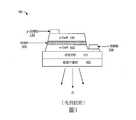
圖1為實例習知氮化物發光二極體(light emitting diode;LED)之圖。FIG. 1 is a diagram of an example of a conventional nitride light emitting diode (LED).
圖2為適用於使得直接接合的微LED結構的晶圓級、晶片陣列級及獨立晶片 級建構實現電接觸點之直接接合的實例LED結構的圖。FIG. 2 is a diagram of an example LED structure suitable for direct bonding of electrical contact points in wafer-level, wafer-array-level, and independent wafer-level constructions of directly bonded micro LED structures.
圖3為以與驅動器電路直接接合操作之圖2之實例LED結構的圖。Figure 3 is a diagram of the example LED structure of Figure 2 operating in direct engagement with the driver circuit.
圖4為製造圖2之LED結構之實例方法的圖。Fig. 4 is a diagram of an example method of manufacturing the LED structure of Fig. 2.
圖5為製造實例LED陣列顯示器之第一階段的圖。Fig. 5 is a diagram of the first stage of manufacturing an example LED array display.
圖6為製造實例LED陣列顯示器之第二階段的圖。Fig. 6 is a diagram of the second stage of manufacturing the example LED array display.
圖7為製造實例LED陣列顯示器之第三階段的圖。Fig. 7 is a diagram of the third stage of manufacturing the example LED array display.
圖8為製造實例LED陣列顯示器之第四階段的圖。Fig. 8 is a diagram of the fourth stage of manufacturing the example LED array display.
圖9為製造實例LED陣列顯示器之第五階段的圖。Fig. 9 is a diagram of the fifth stage of manufacturing the example LED array display.
圖10為已完成之LED陣列顯示器及任選組件之圖。Figure 10 is a diagram of the completed LED array display and optional components.
圖11為製造直接接合的LED結構之實例方法的方塊圖。Figure 11 is a block diagram of an example method of manufacturing a directly bonded LED structure.
本揭示描述實例直接接合的發光二極體(light emitting diode;LED)陣列及應用。描述用於形成主動驅動mLED(microLED)結構及顯示單元之新穎方法,該方法包括將III-V化合物半導體mLED陣列接合至矽驅動器晶片以形成主動驅動mLED顯示單元之實例方法。此等方法中之一些可用於量產mLED陣列顯示器。This disclosure describes examples of directly bonded light emitting diode (LED) arrays and applications. A novel method for forming an actively driven mLED (microLED) structure and display unit is described. The method includes an example method of bonding a III-V compound semiconductor mLED array to a silicon driver chip to form an actively driven mLED display unit. Some of these methods can be used for mass production of mLED array displays.
實例方法及結構Example method and structure
圖1展示藍寶石基板100上方之發光二極體(light emitting diode;LED)之習知磊晶層結構50的實例,說明且比較用於本文中所描述之實例結構及方法之一些LED組件。舉例而言,實例習知LED結構50可產生綠光或藍光。半導體材料層化於載體上,諸如藍寶石基板100。GaN與藍寶石100之間的晶格常數及熱膨脹係數之較大失配將造成GaN膜中之較高結晶疵點密度,其引起裝置效能之降低;從而使晶格及CTE匹配緩衝材料101沉積於藍寶石100上以生長GaN。類 似於習知LED結構50之光電裝置利用半導體摻雜,例如將少量矽或鍺添加至氮化鎵(gallium nitride;GaN)以使GaN成為用於電子(n型)n-GaN 102之導體,且將少量鎂添加至氮化鎵(gallium nitride;GaN)以使GaN形成於導體中以用於空穴(電子空穴)(p型)p-GaN 104。n-GaN 102之層與p-GaN 104之層之間包夾發光量子井或多量子井(multiple quantum well;MQW)材料(諸如氮化銦鎵InGaN)之超薄層,該超薄層比n-GaN 102及p-GaN 104之任一者具有更小之帶隙(及稍微較小之導電性),該氮化銦鎵InGaN為由混合氮化鎵(gallium nitride;GaN)與氮化銦(indium nitride;InN)而製成之半導體材料。InGaN為三元第III族/第V族直接帶隙半導體。實例InGaN/GaN或InGaN MQW層106提供量子約束,或分散能量子頻帶,在子頻帶中,載波可僅具有分散能量值,在光學裝置中提供較佳效能。習知LED結構50於所使用之編號或層中可具有許多變型,且材料用於每一層。在圖1中,層,且尤其MQW層106未按相對比例展示。FIG. 1 shows an example of a conventional
實例習知LED結構50之特徵在於n接觸點108及p接觸點110位於習知LED結構50之不同表面上之不同垂直水平處。p接觸點110與n接觸點108之間的垂直高度之差藉由電線接合或焊料連接習知地補償。或者,實例習知結構50可具有未暴露之n接觸點108(未展示)。Examples The characteristic of the
圖2至圖3展示用於將含有III-V半導體元件之LED組件直接接合至驅動器電路以用於製造mLED陣列顯示器的實例LED結構200及方法綜覽。實例LED結構200提供超平面接合介面202,該超平面接合介面介面202藉由例如使用由絕緣體204(諸如氧化矽)包圍且暴露於具有超平面接合介面202上之各別共面導電佔據面積206及208的超平面接合介面202上之n接觸點108及p接觸點110兩者之化學機械拋光(chemical-mechanical polishing;CMP)而形成平面。2 to 3 show an overview of an
n接觸點108及p接觸點110可由金屬或合金金屬之組合或促進直接接合的層壓金屬製成。除金屬組合物以外,超平面接合介面202自身亦促進n 接觸點108與p接觸點110之間的直接接合及各別導電面之接合。超平面接合介面202藉由鑲嵌方法製造,例如亦為超淨,且在幾十奈米內平坦,諸如小於波長為546.1奈米之單色綠光或為632.8奈米之氦氖紅色雷射光之照明源的1/4。在一些具體實例中,平面拋光表面202之粗糙度小於照明源之波長的5%且優選地小於10nm。The n-
圖3展示圖2之實例LED結構200與晶片304上之驅動器電路302之間、用以形成諸如薄膜電晶體(thin-film transistor;TFT)驅動器之LED電路的實例直接接合方法300。實例直接接合方法300可在獨立晶片之層級上,或在晶片陣列層級下或在晶圓級下執行。對於後續剝離及薄化,晶圓級直接接合可為最佳方式。3 shows an example direct bonding method 300 for forming an LED circuit such as a thin-film transistor (TFT) driver between the
在實施方案中,可將mLED超平面接合介面202接合至例如矽基驅動器積體電路(integrated circuit;IC)304之各別超平面接合介面306。超平面接合介面306可具有頂部有平面氧化矽層及銅(Cu)襯墊之接觸表面以促進直接接合(例如經由ZiBond®牌方法或DBI®牌方法直接接合)以形成LED電路(Xperi Corporation,San Jose,CA)。在實施方案中,藍寶石基板100可隨後經雷射剝離。若需要,則頂部及底部側兩者可經薄化進一步使得整個疊層可撓。In an embodiment, the mLED
圖4展示實例結構製造之階段,說明用於製造適用於與例如矽驅動器IC 304直接接合的LED結構200的實例方法流程。FIG. 4 shows the stages of manufacturing an example structure, illustrating an example method flow for manufacturing an
在實例方法流程之第一階段400中,諸如藍寶石基板100之實例晶圓與n-GaN 102、InGaN MQW 106及p-GaN 104之起始磊晶層一起累積。In the
在實例方法流程之第二階段402中,圖案化且蝕刻頂部磊晶層以在特定位置404處暴露n-GaN層102。雖然在晶粒之邊緣處展示單個暴露位置404,但可存在多於一個位置。舉例而言,一或多個穿孔可暴露n-GaN層102。圖案化光阻可保留於其上。In the
在實例方法流程之第三階段406中,沉積諸如氧化矽層204之絕緣體或介電質以至少在接觸襯墊之位置處覆蓋經暴露p-GaN 104及經暴露n-GaN 102兩者。In the
在實例方法流程之第四階段408中,於p-GaN 104及n-GaN 102層上方圖案化且蝕刻氧化矽層204以使得腔體410穿透氧化矽204以用於使導電金屬變為LED結構200之電極。在一實施方案中,p-GaN 104層及MQW 106層之總厚度為近似於2μm,使結構在此階段適用於單步蝕刻及金屬化(MQW層106,未按比例展示)。可形成此類腔體410中之一或多者以形成接觸n-GaN 102層及p-GaN 104層之一或多個電極。In the
在替代實施方案中,實例方法使平面氧化矽層204如在上述第三階段406中沉積,隨後使用ZiBond®牌直接接合方法或其他直接接合技術直接與驅動晶片304一起接合此氧化物表面。隨後,貫穿矽之通孔(through-silicon-via;TSV)經打孔以建立自n接觸點108及p接觸點110至驅動器晶片304之電連接性。In an alternative embodiment, the example method deposits the planar
在實例方法流程之第五階段412中,腔體410可使用導電材料414金屬化。在一實施方案中,可塗佈且形成障壁及晶種層塗層416,隨後用有導體414填充之腔體,繼之以退火及化學機械平坦化(chemical-mechanical planarization;CMP)。在一實施方案中,可將諸如銦之低熔化溫度金屬塗佈於腔體中。In the
在實例方法之第六階段418中,實例LED結構200之頂部表面經電漿激活420以用於直接接合操作。電漿激活420可視情況用於一些類型之直接接合技術,而在其它直接接合技術中,電漿激活步驟420例如在接觸接合期間促進兩個金屬表面之間的接合強度。電漿激活420亦可應用於待接合於驅動器晶片304上之相對表面。In the
在各種實施方案中,圖4中描繪之實例方法流程可包括挑選且傳 送具有高產量之許多小LED晶片,且在極精細間距下直接接合,例如在小於1mm之間距(甚至用於製造微投影儀之更小間距)下,以及在0.05mm間距下,且在各種實施方案中一直降至具有6um凸塊之12μm間距。像素陣列光學件達成LED晶粒200與Si晶粒304之較高平行性。可實現諸如薄化及雷射剝離之後處理,此係由於直接接合塗佈導致平面形貌及較強接合介面達成。In various embodiments, the example method flow depicted in FIG. 4 may include selecting and transferring many small LED chips with high yields, and directly bonding them at very fine pitches, for example, between less than 1mm (even for manufacturing micro-projection It has been reduced to 12μm pitch with 6um bumps in various implementations under the smaller pitch of the instrument), and at the 0.05mm pitch, and in various embodiments. The pixel array optics achieve high parallelism between the LED die 200 and the Si die 304. It can achieve post-processing such as thinning and laser peeling, which is achieved by direct bonding coating resulting in a flat topography and a strong bonding interface.
圖5至9展示用於產生薄、透明且可撓之mLED陣列顯示器500之實例方法,在該方法中,具有藉由圖4之方法形成之LED結構200之晶圓502現接合至(例如)CMOS驅動器晶片晶圓504以形成透明且可撓之陣列顯示器500。FIGS. 5 to 9 show an example method for producing a thin, transparent, and flexible
在圖5中,在一實施方案中,在LED裝置晶圓502上之平面及經激活表面形成之後,CMOS晶圓504使用CMP或獲得超平面表面及電漿激活420之其他方法平面化。In FIG. 5, in one embodiment, after the planar and activated surfaces on the
在圖6中,接合兩個晶圓502及504。舉例而言,具有LED結構200且具有n接觸點108與p接觸點110之共面接合表面的第一晶圓502,以及具有CMOS驅動器晶片304之第二晶圓504接合在一起以用於金屬導體之間(且在一實施方案中亦在非金屬介電質表面602之間)的直接接合。與第二晶圓504之經暴露氧化矽相接觸的第一晶圓502之經暴露氧化矽首先經由如同ZiBond®牌直接接合方法之氧化物接合而接合。各別晶圓502及504之金屬接觸襯墊在如同DBI®牌直接接合方法之高於室溫之退火期間形成金屬至金屬接合。接合介面604可在近似於100℃至200℃下退火以形成較強直接接合介面,諸如ZiBond®或DBI®牌直接接合介面。In FIG. 6, two
可沉積諸如分佈式布拉格反射器(distributed Bragg reflector;DBR)606(未按相對比例展示)之光學反射塗層以藉由挑選第一晶圓502與第二晶圓504之間的介面(606)處之晶圓502之頂部上之介電層的不同類型及厚度來增大封裝之光輸出。可替代地,DBR 606亦可在接合之前於第二晶圓504之頂 部上形成。在DBR 606之此定向中,光可自裝置之藍寶石側逸出。若DBR 606於第一晶圓502上形成,則薄電介質需要在圖4中展示之方法之第二階段402或第三階段406結束時沉積。DBR 606為由具有變化折射率或藉由例如介電質之厚度之一些特徵的週期性變化以引起有效折射率之週期性變化之交替材料之多個層形成的結構。舉例而言,介電質塗層之此等薄層可為氧化矽、氟化鎂、五氧化鉭、硫化鋅以及二氧化鈦之組合。化合物晶圓502之頂部表面上之氧化矽SiOx層亦可充當隨後使用諸如ZiBond®或DBI®方法之直接接合技術直接接合至晶圓504之塗層的最後一層。Optical reflective coatings such as distributed Bragg reflector (DBR) 606 (not shown to a relative scale) can be deposited by selecting the interface between the
在另一具體實例中,DBR可於藍寶石與n-GaN之間處形成。在此定向中,光將朝向CMOS晶圓504反射。然而,歸因於CMOS晶片將阻礙逸出路徑,將逸出較少量的光。In another specific example, the DBR can be formed between sapphire and n-GaN. In this orientation, the light will reflect towards the
在圖7中,薄膜電晶體(thin-film transistor;TFT)底板可經薄化702,該薄化702可藉由ZiBond®牌直接接合方法來促進。隨後,經薄化底板之無電晶體部分704亦可經蝕刻掉。在此具體實例中,一或多個n接觸點108及p接觸點110之位置可經設計以使得其可在底板之蝕刻之後自背側暴露;且從而可經接觸以用於與背側之電力傳遞。In FIG. 7, the thin-film transistor (TFT) substrate can be thinned 702, and the thinning 702 can be facilitated by the ZiBond® brand direct bonding method. Subsequently, the
在圖8中,經薄化及蝕刻之電晶體表面可使用聚醯亞胺(polyimide;PI)層802或用於保護之任何其他介電材料來塗佈。In FIG. 8, the thinned and etched surface of the transistor can be coated with a polyimide (PI)
在圖9中,可對藍寶石基板層100執行雷射剝離,且晶圓502之此經暴露側隨後使用可撓有機基板902來塗佈。In FIG. 9, laser lift-off can be performed on the
在另一具體實例中,用以由電晶體底板藉由PI蝕刻且回填之方法可在藍寶石基板層100之雷射剝離之前省略。在此具體實例中,可能在底板中需要一或多個貫穿電極以用於對電極之電力傳遞。In another specific example, the method for etching and backfilling from the transistor substrate by PI can be omitted before the laser stripping of the
圖10展示於建立有直接接合的實例透明且可撓之mLED陣列顯 示器500之所有側上之可用的可操作通路。此變通性至少部分地由於可能使用諸如DBI®及ZiBond®牌接合方法之直接接合的較強接合,該直接接合導致最終結構能夠耐受於結構500之多個側上之其他處理。舉例而言,除剝離透明(例如藍寶石)基板100以使得可撓顯示器500接合至可撓有機基板902以外,可應用後研磨且執行進一步剝離以使得顯示器更薄、更透明且更可撓。Figure 10 shows the operable pathways available on all sides of an example transparent and flexible
可將mLED陣列顯示器500之背側添加至具有背側堆積層1002上以用於其他3D整合以附接至記憶體、印刷電路板(printed circuit board;PCB)、觸覺及其他感測器等等。The backside of the
可將一或多個光波導1004整合於透明基板902之頂部上以自LED元件傳輸光信號,且亦可添加用於電信號之線路。在一實施方案中,一或多個光波導1004藉由直接接合技術附接至實例LED陣列顯示器500。One or more
在實例mLED陣列顯示器500之側上,可添加邊緣發射組態1006,及/或該些側上之類似於頂部上之一或多個光波導1004的光波導。在此具體實例中,可能在LED裝置200之兩側上需要反射器,在層902處,以及在直接接合(例如ZiBond®)介面604/606處。On the sides of the example
實例mLED陣列顯示器500之結構實現例如用於太陽能電池及太陽能電池板之化合物半導體之多接面堆疊。The structure of the example
實例mLED陣列顯示器500之側亦可容納冷卻結構1008。The side of the example
如在圖8中,在移除藍寶石層100之後,表面可變粗糙且添加氧化銦錫(indium tin oxide;ITO)以改良LED之電導率。As in FIG. 8, after the
剛剛上文所描述且說明之實例步驟提供直接接合的發光二極體(light emitting diode;LED)陣列500,例如mLED之陣列,其中例如在晶圓級方法中,第III至第V族半導體元件直接接合至LED驅動器電路。經由直接接合方法形成之陣列500可為可撓的,且具有光學透明表面。The example steps described and illustrated just above provide a direct-bonded light emitting diode (LED)
一般而言,基於實例化合物半導體之LED陣列裝置500經形成以具有由共面金屬區域及介電質區域組成之平面表面。共面金屬區域電連接至每一LED元件之化合物半導體之激活區域。Generally speaking, the
上文基於化合物半導體之LED陣列結構500可包括與以直接接合方式連接之基於CMOS之裝置的接合。基於化合物半導體之LED陣列裝置500之金屬區域及介電質區域可直接接合至基於CMOS之裝置的各別金屬區域及介電質區域。雖然對晶圓級方法進行描述,但圖5至圖9之實例方法仍不僅可用於晶圓至晶圓(wafer-to-wafer;W2W)方法,且亦可用於晶粒至晶粒(die-to-die;D2D),或一或多個晶粒至晶圓(dies-to-wafer;D2W)方法。The above compound semiconductor-based
所得實例LED陣列結構500亦可具有其他特性及特徵: 所得LED陣列結構500可缺少基於第III至第V族之半導體發光裝置生長之基板。此外,基於第III至第V族半導體之發光裝置之微觀結構的表面可有利地粗糙化以用於改良之光提取。The resulting example
用於經由諸如DBI®牌直接接合方法之直接接合方法電連接至n-GaN 102及p-GaN 104激活區域之電極形狀可經專門設計,諸如用於n-GaN 102區域之電極或接觸點108的框追蹤點陣列,及用於p-GaN 104區域之電極或接觸點110的圓形或方形區域中之點陣列。The shape of electrodes used to electrically connect to the active regions of n-
實例方法Instance method
圖11展示製造直接接合LED結構之實例方法1100。在流程圖中,實例方法1100之操作展示於獨立區塊中。Figure 11 shows an
在區塊1102處,LED結構經製造以具有在包含LED結構之平面接合介面之第一表面上共面的p型與n型半導體元件之電接觸點。At
在區塊1104處,第一表面直接接合至包含用於LED結構之驅動器電路之平面接合介面的第二表面。At
用於實例方法1100中之直接接合操作(諸如ZiBond®或DBI®牌直接接合方法)可以晶圓級、單晶片級或晶片陣列級方法塗佈。The direct bonding operations used in the example method 1100 (such as ZiBond® or DBI® brand direct bonding methods) can be applied at the wafer level, single wafer level, or wafer array level methods.
在本說明書及所附申請專利範圍中:術語「連接(connect/connection/connected)」、「與…相連接」及「連接(connecting)」用以意謂「與…直接連接」或「經由一或多個元件與…相連接」。術語「耦接(couple/coupling/coupled)」、「耦接至一起」及「與…耦接」用以意謂「直接地耦接至一起」或「經由一或多個元件耦接至一起」。In the scope of this specification and the attached patent application: the terms "connect/connection/connected", "connected with" and "connecting" are used to mean "directly connected with" or "via a connection". Or multiple components are connected with...". The terms "couple/coupling/coupled", "coupled together" and "coupled with" are used to mean "directly coupled together" or "coupled together via one or more elements" ".
儘管本揭示已對有限數目之具體實例進行揭示,但受益於本發明之熟習此項技術者將瞭解,本說明書所給定之多個修改及變化為可能的。意欲所附申請專利範圍涵蓋如在本揭示之真實精神及範圍內的此類修改及變化。Although the present disclosure has disclosed a limited number of specific examples, those skilled in the art who benefit from the present invention will understand that many modifications and changes given in this specification are possible. It is intended that the scope of the attached patent application covers such modifications and changes as within the true spirit and scope of this disclosure.
100‧‧‧藍寶石基板100‧‧‧Sapphire substrate
102‧‧‧n-GaN層102‧‧‧n-GaN layer
104‧‧‧p-GaN層104‧‧‧p-GaN layer
106‧‧‧MQW層106‧‧‧MQW layer
108‧‧‧n接觸點108‧‧‧n contact point
110‧‧‧p接觸點110‧‧‧p contact point
202‧‧‧超平面接合介面202‧‧‧Hyperplane bonding interface
204‧‧‧絕緣體/氧化矽層204‧‧‧Insulator/silicon oxide layer
206‧‧‧佔據面積206‧‧‧Occupied area
208‧‧‧佔據面積208‧‧‧Occupied area
Claims (14)
Translated fromChineseApplications Claiming Priority (4)
| Application Number | Priority Date | Filing Date | Title |
|---|---|---|---|
| US201762472363P | 2017-03-16 | 2017-03-16 | |
| US62/472,363 | 2017-03-16 | ||
| US15/919,570 | 2018-03-13 | ||
| US15/919,570US10629577B2 (en) | 2017-03-16 | 2018-03-13 | Direct-bonded LED arrays and applications |
Publications (2)
| Publication Number | Publication Date |
|---|---|
| TW201843830A TW201843830A (en) | 2018-12-16 |
| TWI742256Btrue TWI742256B (en) | 2021-10-11 |
Family
ID=63522473
Family Applications (1)
| Application Number | Title | Priority Date | Filing Date |
|---|---|---|---|
| TW107108645ATWI742256B (en) | 2017-03-16 | 2018-03-14 | Direct-bonded led arrays and applications |
Country Status (3)
| Country | Link |
|---|---|
| US (7) | US10629577B2 (en) |
| TW (1) | TWI742256B (en) |
| WO (1) | WO2018169968A1 (en) |
Families Citing this family (138)
| Publication number | Priority date | Publication date | Assignee | Title |
|---|---|---|---|---|
| US7109092B2 (en) | 2003-05-19 | 2006-09-19 | Ziptronix, Inc. | Method of room temperature covalent bonding |
| US8735219B2 (en) | 2012-08-30 | 2014-05-27 | Ziptronix, Inc. | Heterogeneous annealing method and device |
| US10886250B2 (en) | 2015-07-10 | 2021-01-05 | Invensas Corporation | Structures and methods for low temperature bonding using nanoparticles |
| US9953941B2 (en) | 2015-08-25 | 2018-04-24 | Invensas Bonding Technologies, Inc. | Conductive barrier direct hybrid bonding |
| US10204893B2 (en) | 2016-05-19 | 2019-02-12 | Invensas Bonding Technologies, Inc. | Stacked dies and methods for forming bonded structures |
| US11176450B2 (en) | 2017-08-03 | 2021-11-16 | Xcelsis Corporation | Three dimensional circuit implementing machine trained network |
| US10672663B2 (en) | 2016-10-07 | 2020-06-02 | Xcelsis Corporation | 3D chip sharing power circuit |
| US10580735B2 (en) | 2016-10-07 | 2020-03-03 | Xcelsis Corporation | Stacked IC structure with system level wiring on multiple sides of the IC die |
| TWI822659B (en) | 2016-10-27 | 2023-11-21 | 美商艾德亞半導體科技有限責任公司 | Structures and methods for low temperature bonding |
| US10002844B1 (en) | 2016-12-21 | 2018-06-19 | Invensas Bonding Technologies, Inc. | Bonded structures |
| US20180182665A1 (en) | 2016-12-28 | 2018-06-28 | Invensas Bonding Technologies, Inc. | Processed Substrate |
| CN117878055A (en) | 2016-12-28 | 2024-04-12 | 艾德亚半导体接合科技有限公司 | Stacking substrate processing |
| TWI837879B (en) | 2016-12-29 | 2024-04-01 | 美商艾德亞半導體接合科技有限公司 | Bonded structures with integrated passive component |
| WO2018169968A1 (en) | 2017-03-16 | 2018-09-20 | Invensas Corporation | Direct-bonded led arrays and applications |
| US10515913B2 (en) | 2017-03-17 | 2019-12-24 | Invensas Bonding Technologies, Inc. | Multi-metal contact structure |
| US10508030B2 (en) | 2017-03-21 | 2019-12-17 | Invensas Bonding Technologies, Inc. | Seal for microelectronic assembly |
| FR3065321B1 (en)* | 2017-04-14 | 2019-06-21 | Commissariat A L'energie Atomique Et Aux Energies Alternatives | METHOD FOR MANUFACTURING EMISSIVE LED DISPLAY DEVICE |
| US10269756B2 (en) | 2017-04-21 | 2019-04-23 | Invensas Bonding Technologies, Inc. | Die processing |
| US10879212B2 (en) | 2017-05-11 | 2020-12-29 | Invensas Bonding Technologies, Inc. | Processed stacked dies |
| US10446441B2 (en) | 2017-06-05 | 2019-10-15 | Invensas Corporation | Flat metal features for microelectronics applications |
| US10217720B2 (en) | 2017-06-15 | 2019-02-26 | Invensas Corporation | Multi-chip modules formed using wafer-level processing of a reconstitute wafer |
| US20200152841A1 (en)* | 2017-07-31 | 2020-05-14 | Yale University | Nanoporous micro-led devices and methods for making |
| US10840205B2 (en) | 2017-09-24 | 2020-11-17 | Invensas Bonding Technologies, Inc. | Chemical mechanical polishing for hybrid bonding |
| US11031285B2 (en) | 2017-10-06 | 2021-06-08 | Invensas Bonding Technologies, Inc. | Diffusion barrier collar for interconnects |
| US11011503B2 (en)* | 2017-12-15 | 2021-05-18 | Invensas Bonding Technologies, Inc. | Direct-bonded optoelectronic interconnect for high-density integrated photonics |
| US11557703B2 (en)* | 2017-12-21 | 2023-01-17 | Lumileds Llc | Light intensity adaptive LED sidewalls |
| US11380597B2 (en) | 2017-12-22 | 2022-07-05 | Invensas Bonding Technologies, Inc. | Bonded structures |
| WO2019147738A1 (en)* | 2018-01-23 | 2019-08-01 | Light Share, LLC | Full-color monolithic micro-led pixels |
| US10727219B2 (en) | 2018-02-15 | 2020-07-28 | Invensas Bonding Technologies, Inc. | Techniques for processing devices |
| US11169326B2 (en) | 2018-02-26 | 2021-11-09 | Invensas Bonding Technologies, Inc. | Integrated optical waveguides, direct-bonded waveguide interface joints, optical routing and interconnects |
| US11256004B2 (en) | 2018-03-20 | 2022-02-22 | Invensas Bonding Technologies, Inc. | Direct-bonded lamination for improved image clarity in optical devices |
| US10991804B2 (en) | 2018-03-29 | 2021-04-27 | Xcelsis Corporation | Transistor level interconnection methodologies utilizing 3D interconnects |
| US11056348B2 (en) | 2018-04-05 | 2021-07-06 | Invensas Bonding Technologies, Inc. | Bonding surfaces for microelectronics |
| US11244916B2 (en) | 2018-04-11 | 2022-02-08 | Invensas Bonding Technologies, Inc. | Low temperature bonded structures |
| US10790262B2 (en) | 2018-04-11 | 2020-09-29 | Invensas Bonding Technologies, Inc. | Low temperature bonded structures |
| US10964664B2 (en) | 2018-04-20 | 2021-03-30 | Invensas Bonding Technologies, Inc. | DBI to Si bonding for simplified handle wafer |
| US11004757B2 (en) | 2018-05-14 | 2021-05-11 | Invensas Bonding Technologies, Inc. | Bonded structures |
| US11276676B2 (en) | 2018-05-15 | 2022-03-15 | Invensas Bonding Technologies, Inc. | Stacked devices and methods of fabrication |
| US10923413B2 (en) | 2018-05-30 | 2021-02-16 | Xcelsis Corporation | Hard IP blocks with physically bidirectional passageways |
| KR20210009426A (en) | 2018-06-13 | 2021-01-26 | 인벤사스 본딩 테크놀로지스 인코포레이티드 | TV as a pad |
| US11393779B2 (en) | 2018-06-13 | 2022-07-19 | Invensas Bonding Technologies, Inc. | Large metal pads over TSV |
| US10910344B2 (en) | 2018-06-22 | 2021-02-02 | Xcelsis Corporation | Systems and methods for releveled bump planes for chiplets |
| WO2020010056A1 (en) | 2018-07-03 | 2020-01-09 | Invensas Bonding Technologies, Inc. | Techniques for joining dissimilar materials in microelectronics |
| US11158606B2 (en) | 2018-07-06 | 2021-10-26 | Invensas Bonding Technologies, Inc. | Molded direct bonded and interconnected stack |
| US11462419B2 (en) | 2018-07-06 | 2022-10-04 | Invensas Bonding Technologies, Inc. | Microelectronic assemblies |
| US12406959B2 (en) | 2018-07-26 | 2025-09-02 | Adeia Semiconductor Bonding Technologies Inc. | Post CMP processing for hybrid bonding |
| US11515291B2 (en) | 2018-08-28 | 2022-11-29 | Adeia Semiconductor Inc. | Integrated voltage regulator and passive components |
| US20200075533A1 (en) | 2018-08-29 | 2020-03-05 | Invensas Bonding Technologies, Inc. | Bond enhancement in microelectronics by trapping contaminants and arresting cracks during direct-bonding processes |
| US11011494B2 (en) | 2018-08-31 | 2021-05-18 | Invensas Bonding Technologies, Inc. | Layer structures for making direct metal-to-metal bonds at low temperatures in microelectronics |
| US11158573B2 (en) | 2018-10-22 | 2021-10-26 | Invensas Bonding Technologies, Inc. | Interconnect structures |
| TWI688317B (en)* | 2018-10-31 | 2020-03-11 | 台灣愛司帝科技股份有限公司 | Led mounted method and device |
| EP3667745B1 (en)* | 2018-12-10 | 2023-03-22 | IMEC vzw | Method for obtaining light emitting diodes reconstituted over a carrier substrate |
| EP3667721A1 (en)* | 2018-12-10 | 2020-06-17 | IMEC vzw | Method for fabricating an optical device |
| US11244920B2 (en) | 2018-12-18 | 2022-02-08 | Invensas Bonding Technologies, Inc. | Method and structures for low temperature device bonding |
| JP7348520B2 (en)* | 2018-12-25 | 2023-09-21 | 日亜化学工業株式会社 | Light emitting device and display device |
| CN113330557A (en) | 2019-01-14 | 2021-08-31 | 伊文萨思粘合技术公司 | Bonding structure |
| US11349052B2 (en) | 2019-02-05 | 2022-05-31 | Facebook Technologies, Llc | Bonding interface for hybrid TFT-based micro display projector |
| US11355665B2 (en)* | 2019-06-19 | 2022-06-07 | Facebook Technologies, Llc | Process flow for hybrid TFT-based micro display projector |
| US20220208738A1 (en)* | 2019-02-21 | 2022-06-30 | Vuereal Inc. | Optoelectronic solid state array |
| US11387202B2 (en) | 2019-03-01 | 2022-07-12 | Invensas Llc | Nanowire bonding interconnect for fine-pitch microelectronics |
| US11901281B2 (en) | 2019-03-11 | 2024-02-13 | Adeia Semiconductor Bonding Technologies Inc. | Bonded structures with integrated passive component |
| US10854578B2 (en) | 2019-03-29 | 2020-12-01 | Invensas Corporation | Diffused bitline replacement in stacked wafer memory |
| KR102137688B1 (en)* | 2019-04-12 | 2020-08-28 | 임성규 | Self-Customized Mcro LED Jewelry |
| US11373963B2 (en) | 2019-04-12 | 2022-06-28 | Invensas Bonding Technologies, Inc. | Protective elements for bonded structures |
| US11205625B2 (en) | 2019-04-12 | 2021-12-21 | Invensas Bonding Technologies, Inc. | Wafer-level bonding of obstructive elements |
| US11355404B2 (en) | 2019-04-22 | 2022-06-07 | Invensas Bonding Technologies, Inc. | Mitigating surface damage of probe pads in preparation for direct bonding of a substrate |
| US11158761B2 (en) | 2019-05-07 | 2021-10-26 | Facebook Technologies, Llc | Bonding methods for light emitting diodes |
| DE102019111816A1 (en) | 2019-05-07 | 2020-11-12 | OSRAM Opto Semiconductors Gesellschaft mit beschränkter Haftung | METHOD OF MANUFACTURING A COMPONENT AND COMPONENT |
| US11385278B2 (en) | 2019-05-23 | 2022-07-12 | Invensas Bonding Technologies, Inc. | Security circuitry for bonded structures |
| US12374641B2 (en) | 2019-06-12 | 2025-07-29 | Adeia Semiconductor Bonding Technologies Inc. | Sealed bonded structures and methods for forming the same |
| JP7341742B2 (en)* | 2019-06-17 | 2023-09-11 | キヤノン株式会社 | light emitting element |
| US11296053B2 (en) | 2019-06-26 | 2022-04-05 | Invensas Bonding Technologies, Inc. | Direct bonded stack structures for increased reliability and improved yield in microelectronics |
| CN110299377B (en)* | 2019-07-03 | 2022-12-16 | 京东方科技集团股份有限公司 | Display substrate, manufacturing method, and display device |
| KR102780352B1 (en)* | 2019-07-05 | 2025-03-12 | 삼성전자주식회사 | Method of manufacturing light emitting device package and method of manufacturing display panel using the same |
| JP2021019015A (en)* | 2019-07-17 | 2021-02-15 | シャープ福山セミコンダクター株式会社 | Micro light emitting element and image display element |
| CN110707148B (en)* | 2019-09-02 | 2021-08-17 | 华南师范大学 | Epitaxial wafer, manufacturing method of epitaxial wafer, diode and rectifier |
| US12080672B2 (en) | 2019-09-26 | 2024-09-03 | Adeia Semiconductor Bonding Technologies Inc. | Direct gang bonding methods including directly bonding first element to second element to form bonded structure without adhesive |
| US12113054B2 (en) | 2019-10-21 | 2024-10-08 | Adeia Semiconductor Technologies Llc | Non-volatile dynamic random access memory |
| CN110707186A (en)* | 2019-10-21 | 2020-01-17 | 深圳市华星光电半导体显示技术有限公司 | Preparation method of LED display panel |
| CN112713167B (en)* | 2019-10-25 | 2023-05-19 | 成都辰显光电有限公司 | A kind of display panel and the preparation method of display panel |
| US11862602B2 (en) | 2019-11-07 | 2024-01-02 | Adeia Semiconductor Technologies Llc | Scalable architecture for reduced cycles across SOC |
| WO2021102034A1 (en)* | 2019-11-18 | 2021-05-27 | Avicenatech Corp. | High speed and multi-contact leds for data communication |
| KR102848957B1 (en) | 2019-11-26 | 2025-08-20 | 삼성전자주식회사 | Semiconductor light emitting device and method of fabricating the same |
| US11296266B2 (en)* | 2019-11-26 | 2022-04-05 | Facebook Technologies, Llc | LED array having transparent substrate with conductive layer for enhanced current spread |
| US11762200B2 (en) | 2019-12-17 | 2023-09-19 | Adeia Semiconductor Bonding Technologies Inc. | Bonded optical devices |
| US11876076B2 (en) | 2019-12-20 | 2024-01-16 | Adeia Semiconductor Technologies Llc | Apparatus for non-volatile random access memory stacks |
| CN115088068A (en) | 2019-12-23 | 2022-09-20 | 伊文萨思粘合技术公司 | Electrical redundancy for bonded structures |
| US11721653B2 (en) | 2019-12-23 | 2023-08-08 | Adeia Semiconductor Bonding Technologies Inc. | Circuitry for electrical redundancy in bonded structures |
| CN112885777B (en) | 2020-01-07 | 2022-12-09 | 长江存储科技有限责任公司 | Metal-dielectric bonding method and structure |
| WO2021142346A1 (en) | 2020-01-08 | 2021-07-15 | Avicenatech Corp. | Packaging for microleds for chip to chip communication |
| US11355480B1 (en)* | 2020-01-27 | 2022-06-07 | Facebook Technologies, Llc | Micropixellation for alignment-free assembly |
| US12224271B2 (en) | 2020-03-10 | 2025-02-11 | Meta Platforms Technologies, Llc | Integrating control circuits with light emissive circuits with dissimilar wafer sizes |
| EP4122011A4 (en)* | 2020-03-18 | 2024-07-03 | Avicenatech Corp. | Led array for in-plane optical interconnects |
| WO2021188846A1 (en) | 2020-03-19 | 2021-09-23 | Invensas Bonding Technologies, Inc. | Dimension compensation control for directly bonded structures |
| GB2593699B (en)* | 2020-03-30 | 2022-10-26 | Plessey Semiconductors Ltd | Monolithic LED pixel |
| US11742314B2 (en) | 2020-03-31 | 2023-08-29 | Adeia Semiconductor Bonding Technologies Inc. | Reliable hybrid bonded apparatus |
| US11817535B2 (en) | 2020-04-21 | 2023-11-14 | Raysolve Optoelectronics (Suzhou) Company Limited | Light emitting diode structure and method for manufacturing the same |
| WO2021217607A1 (en)* | 2020-04-30 | 2021-11-04 | 重庆康佳光电技术研究院有限公司 | Bonding method, display backplate and display backplate manufacturing system |
| WO2021236361A1 (en) | 2020-05-19 | 2021-11-25 | Invensas Bonding Technologies, Inc. | Laterally unconfined structure |
| US11631647B2 (en) | 2020-06-30 | 2023-04-18 | Adeia Semiconductor Bonding Technologies Inc. | Integrated device packages with integrated device die and dummy element |
| WO2022000385A1 (en)* | 2020-07-01 | 2022-01-06 | 重庆康佳光电技术研究院有限公司 | Manufacturing method for display panel, display panel and display device |
| KR102765871B1 (en) | 2020-07-17 | 2025-02-12 | 삼성디스플레이 주식회사 | Display device and method of fabricating the display device |
| US11764177B2 (en) | 2020-09-04 | 2023-09-19 | Adeia Semiconductor Bonding Technologies Inc. | Bonded structure with interconnect structure |
| US11728273B2 (en) | 2020-09-04 | 2023-08-15 | Adeia Semiconductor Bonding Technologies Inc. | Bonded structure with interconnect structure |
| US11264357B1 (en) | 2020-10-20 | 2022-03-01 | Invensas Corporation | Mixed exposure for large die |
| KR20230097121A (en) | 2020-10-29 | 2023-06-30 | 아데이아 세미컨덕터 본딩 테크놀로지스 인코포레이티드 | Direct bonding method and structure |
| JP2024501017A (en) | 2020-12-28 | 2024-01-10 | アデイア セミコンダクター ボンディング テクノロジーズ インコーポレイテッド | Structure with through-substrate via and method for forming the same |
| JP2024501559A (en) | 2020-12-30 | 2024-01-12 | アデイア セミコンダクター ボンディング テクノロジーズ インコーポレイテッド | Structures with conductive features and methods of forming the same |
| US11710725B2 (en) | 2021-01-22 | 2023-07-25 | Jade Bird Display (shanghai) Limited | Slicing micro-LED wafer and slicing micro-LED chip |
| DE102021101657B4 (en)* | 2021-01-26 | 2024-12-12 | Infineon Technologies Ag | Method for producing a hybrid component |
| WO2022217648A1 (en)* | 2021-04-13 | 2022-10-20 | Raysolve Optoelectronics (Suzhou) Co. Ltd. | Light emitting diode structure and method for manufacturing thereof |
| CN113270438B (en)* | 2021-04-30 | 2024-02-20 | 广东德力光电有限公司 | Manufacturing process of flip micro LED lattice |
| KR20240036698A (en) | 2021-08-02 | 2024-03-20 | 아데이아 세미컨덕터 본딩 테크놀로지스 인코포레이티드 | Protective semiconductor elements for combined structures |
| KR20230020236A (en) | 2021-08-03 | 2023-02-10 | 삼성전자주식회사 | Display apparatus |
| US12336357B2 (en) | 2021-11-24 | 2025-06-17 | Meta Platforms Technologies, Llc | Alignment-free micro-display architecture |
| US12107204B1 (en) | 2021-12-14 | 2024-10-01 | Meta Platforms Technologies, Llc | Small-pitch micro-LEDs |
| CN113990765B (en)* | 2021-12-28 | 2023-04-18 | 深圳市思坦科技有限公司 | Preparation method of flexible light-emitting device, flexible light-emitting device and light-emitting device |
| US20250056921A1 (en)* | 2021-12-31 | 2025-02-13 | Lumileds Llc | Hybrid Bonding With Micro-Light Emitting Diode (LED) Devices |
| WO2023213450A1 (en)* | 2022-05-03 | 2023-11-09 | Ams-Osram International Gmbh | Method for manufacturing a plurality of semiconductor chips and semiconductor chip |
| US12191233B2 (en) | 2022-07-28 | 2025-01-07 | Adeia Semiconductor Bonding Technologies Inc. | Embedded cooling systems and methods of manufacturing embedded cooling systems |
| WO2024138186A1 (en) | 2022-12-23 | 2024-06-27 | Adeia Semiconductor Bonding Technologies Inc. | Embedded cooling systems for advanced device packaging |
| KR20250130348A (en) | 2022-12-29 | 2025-09-01 | 아데이아 세미컨덕터 본딩 테크놀로지스 인코포레이티드 | Embedded cooling assembly for advanced device packaging and method for manufacturing the same |
| KR20250130375A (en) | 2022-12-31 | 2025-09-01 | 아데이아 세미컨덕터 본딩 테크놀로지스 인코포레이티드 | Embedded liquid cooling technology |
| US12341083B2 (en)* | 2023-02-08 | 2025-06-24 | Adeia Semiconductor Bonding Technologies Inc. | Electronic device cooling structures bonded to semiconductor elements |
| TW202516697A (en) | 2023-03-31 | 2025-04-16 | 美商艾德亞半導體接合科技有限公司 | Integrated cooling assemblies including backside power/ground delivery and methods of manufacturing the same |
| WO2024234298A1 (en)* | 2023-05-16 | 2024-11-21 | Jade Bird Display (shanghai) Limited | Transparent electrode structure for micro led display panel |
| US20240387323A1 (en) | 2023-05-17 | 2024-11-21 | Adeia Semiconductor Bonding Technologies Inc. | Integrated cooling assemblies including signal redistribution and methods of manufacturing the same |
| US12191234B2 (en) | 2023-05-17 | 2025-01-07 | Adeia Semiconductor Bonding Technologies Inc. | Integrated cooling assemblies for advanced device packaging and methods of manufacturing the same |
| WO2025091226A1 (en)* | 2023-10-31 | 2025-05-08 | Jade Bird Display (shanghai) Limited | Micro-led array layer and micro-led display panel |
| WO2025096853A1 (en)* | 2023-10-31 | 2025-05-08 | Saphlux, Inc. | Mechanisms for fabricating micro-leds |
| US20250280627A1 (en)* | 2023-11-03 | 2025-09-04 | Google Llc | Methods for led transfer in micro-led displays |
| US12283490B1 (en) | 2023-12-21 | 2025-04-22 | Adeia Semiconductor Bonding Technologies Inc. | Integrated cooling assemblies for advanced device packaging and methods of manufacturing the same |
| US12368087B2 (en) | 2023-12-26 | 2025-07-22 | Adeia Semiconductor Bonding Technologies Inc. | Embedded cooling systems for advanced device packaging and methods of manufacturing the same |
| US12322677B1 (en) | 2024-02-07 | 2025-06-03 | Adeia Semiconductor Bonding Technologies Inc. | Fluid channel geometry optimizations to improve cooling efficiency |
| US12176264B1 (en) | 2024-03-29 | 2024-12-24 | Adeia Semiconductor Bonding Technologies Inc. | Manifold designs for embedded liquid cooling in a package |
| US12336141B1 (en) | 2024-03-29 | 2025-06-17 | Adeia Semiconductor Bonding Technologies Inc. | Cold plate cavity designs for improved thermal performance |
| US12266545B1 (en) | 2024-05-24 | 2025-04-01 | Adeia Semiconductor Bonding Technologies Inc. | Structures and methods for integrated cold plate in XPUs and memory |
| US12412808B1 (en) | 2024-12-20 | 2025-09-09 | Adeia Semiconductor Bonding Technologies Inc. | Cold plate and manifold integration for high reliability |
Citations (3)
| Publication number | Priority date | Publication date | Assignee | Title |
|---|---|---|---|---|
| US20160218128A1 (en)* | 2012-12-13 | 2016-07-28 | Chan- Long Shieh | Active Matrix Light Emitting Diode Array and Projector Display Comprising It |
| US20160343772A1 (en)* | 2014-06-18 | 2016-11-24 | X-Celeprint Limited | Micro assembled led displays and lighting elements |
| TW201834262A (en)* | 2017-03-10 | 2018-09-16 | 錼創科技股份有限公司 | Light-emitting element and display device |
Family Cites Families (438)
| Publication number | Priority date | Publication date | Assignee | Title |
|---|---|---|---|---|
| JPS60257413A (en) | 1984-06-04 | 1985-12-19 | Matsushita Electric Ind Co Ltd | Photoelectric composite device |
| JPH0272642A (en) | 1988-09-07 | 1990-03-12 | Nec Corp | Structure and method for connecting substrates |
| JPH0344067A (en) | 1989-07-11 | 1991-02-25 | Nec Corp | Laminating method of semiconductor substrate |
| US5015052A (en) | 1989-07-20 | 1991-05-14 | Battelle Memorial Institute | Optical modulation at millimeter-wave frequencies |
| CA2083072C (en) | 1991-11-21 | 1998-02-03 | Shinichi Hasegawa | Method for manufacturing polyimide multilayer wiring substrate |
| US6008126A (en) | 1992-04-08 | 1999-12-28 | Elm Technology Corporation | Membrane dielectric isolation IC fabrication |
| US5225797A (en) | 1992-04-27 | 1993-07-06 | Cornell Research Foundation, Inc. | Dielectric waveguide-to-coplanar transmission line transitions |
| KR0137125B1 (en) | 1992-11-16 | 1998-06-15 | 모리시타 요이찌 | Optical waveguide device and manufacturing method |
| US5471090A (en) | 1993-03-08 | 1995-11-28 | International Business Machines Corporation | Electronic structures having a joining geometry providing reduced capacitive loading |
| US5363464A (en) | 1993-06-28 | 1994-11-08 | Tangible Domain Inc. | Dielectric/conductive waveguide |
| EP0651449B1 (en) | 1993-11-01 | 2002-02-13 | Matsushita Electric Industrial Co., Ltd. | Electronic component and method for producing the same |
| US5408053A (en) | 1993-11-30 | 1995-04-18 | Hughes Aircraft Company | Layered planar transmission lines |
| US5472914A (en)* | 1994-07-14 | 1995-12-05 | The United States Of America As Represented By The Secretary Of The Air Force | Wafer joined optoelectronic integrated circuits and method |
| KR960009074A (en) | 1994-08-29 | 1996-03-22 | 모리시다 요이치 | Semiconductor device and manufacturing method thereof |
| DE4433330C2 (en) | 1994-09-19 | 1997-01-30 | Fraunhofer Ges Forschung | Method for producing semiconductor structures with advantageous high-frequency properties and a semiconductor wafer structure |
| US5818631A (en) | 1994-11-16 | 1998-10-06 | Raytheon Company | Electrically conducting, directly bonded infrared windows |
| JP3979687B2 (en) | 1995-10-26 | 2007-09-19 | アプライド マテリアルズ インコーポレイテッド | Method for improving film stability of halogen-doped silicon oxide films |
| US6404550B1 (en) | 1996-07-25 | 2002-06-11 | Seiko Epson Corporation | Optical element suitable for projection display apparatus |
| JPH10189671A (en) | 1996-12-24 | 1998-07-21 | Sony Corp | Probing pad structure of semiconductor wafer |
| JP3210889B2 (en) | 1997-01-14 | 2001-09-25 | シャープ株式会社 | Orthogonal dual polarization waveguide input device and satellite broadcast receiving converter using the same |
| US6221753B1 (en) | 1997-01-24 | 2001-04-24 | Micron Technology, Inc. | Flip chip technique for chip assembly |
| GB2315595B (en) | 1997-02-07 | 1998-06-10 | Bookham Technology Ltd | Device for re-directing light fromoptical waveguide |
| JP4032454B2 (en) | 1997-06-27 | 2008-01-16 | ソニー株式会社 | Manufacturing method of three-dimensional circuit element |
| US6097096A (en) | 1997-07-11 | 2000-08-01 | Advanced Micro Devices | Metal attachment method and structure for attaching substrates at low temperatures |
| US6180496B1 (en) | 1997-08-29 | 2001-01-30 | Silicon Genesis Corporation | In situ plasma wafer bonding method |
| JP3307307B2 (en) | 1997-12-19 | 2002-07-24 | 株式会社村田製作所 | Multilayer type high frequency electronic components |
| JP3832076B2 (en) | 1998-02-16 | 2006-10-11 | セイコーエプソン株式会社 | Polarized illumination device and projection display device |
| US6090636A (en) | 1998-02-26 | 2000-07-18 | Micron Technology, Inc. | Integrated circuits using optical waveguide interconnects formed through a semiconductor wafer and methods for forming same |
| US6762796B1 (en) | 1998-08-10 | 2004-07-13 | Olympus Optical Co., Ltd. | Image pickup module having integrated lens and semiconductor chip |
| JP2000100679A (en) | 1998-09-22 | 2000-04-07 | Canon Inc | Micro-region solid-state bonding method between substrates by thinning and device structure |
| JP3532788B2 (en) | 1999-04-13 | 2004-05-31 | 唯知 須賀 | Semiconductor device and manufacturing method thereof |
| US6242324B1 (en) | 1999-08-10 | 2001-06-05 | The United States Of America As Represented By The Secretary Of The Navy | Method for fabricating singe crystal materials over CMOS devices |
| JP2001102479A (en) | 1999-09-27 | 2001-04-13 | Toshiba Corp | Semiconductor integrated circuit device and method of manufacturing the same |
| US6984571B1 (en) | 1999-10-01 | 2006-01-10 | Ziptronix, Inc. | Three dimensional device integration method and integrated device |
| CA2314723A1 (en) | 1999-12-23 | 2001-06-23 | Pierre Simon Joseph Berini | Optical waveguide structures |
| US6801691B2 (en) | 1999-12-23 | 2004-10-05 | Spectalis Corp. | Optical waveguide structures |
| US6614960B2 (en) | 1999-12-23 | 2003-09-02 | Speotalis Corp. | Optical waveguide structures |
| US6300161B1 (en) | 2000-02-15 | 2001-10-09 | Alpine Microsystems, Inc. | Module and method for interconnecting integrated circuits that facilitates high speed signal propagation with reduced noise |
| US6902987B1 (en) | 2000-02-16 | 2005-06-07 | Ziptronix, Inc. | Method for low temperature bonding and bonded structure |
| US6418029B1 (en) | 2000-02-28 | 2002-07-09 | Mckee James S. | Interconnect system having vertically mounted passive components on an underside of a substrate |
| DE10120248A1 (en) | 2000-04-26 | 2002-03-28 | Kyocera Corp | Structure for connecting a non-radiating dielectric waveguide and a metal waveguide, transmitter / receiver module for millimeter waves and transmitter / receiver for millimeter waves |
| US6429532B1 (en) | 2000-05-09 | 2002-08-06 | United Microelectronics Corp. | Pad design |
| JP4322402B2 (en) | 2000-06-22 | 2009-09-02 | 大日本印刷株式会社 | Printed wiring board and manufacturing method thereof |
| AU2001266613A1 (en) | 2000-06-30 | 2002-01-14 | Motorola, Inc. | Integrated circuits with optical interconnect |
| JP3440057B2 (en) | 2000-07-05 | 2003-08-25 | 唯知 須賀 | Semiconductor device and manufacturing method thereof |
| WO2002008810A2 (en) | 2000-07-21 | 2002-01-31 | Micro Managed Photons A/S | Surface plasmon polariton band gap structures |
| US6970362B1 (en) | 2000-07-31 | 2005-11-29 | Intel Corporation | Electronic assemblies and systems comprising interposer with embedded capacitors |
| US6423640B1 (en) | 2000-08-09 | 2002-07-23 | Taiwan Semiconductor Manufacturing Co., Ltd. | Headless CMP process for oxide planarization |
| GB2374155A (en) | 2001-03-16 | 2002-10-09 | Bookham Technology Plc | A tapered optical waveguide formed with two substrates |
| GB2373344A (en) | 2001-03-16 | 2002-09-18 | Bookham Technology Plc | Optical coupling using direct bonding |
| US6936854B2 (en) | 2001-05-10 | 2005-08-30 | Canon Kabushiki Kaisha | Optoelectronic substrate |
| US7010183B2 (en) | 2002-03-20 | 2006-03-07 | The Regents Of The University Of Colorado | Surface plasmon devices |
| JP2002353416A (en) | 2001-05-25 | 2002-12-06 | Sony Corp | Semiconductor storage device and method of manufacturing the same |
| JP2003043281A (en) | 2001-07-26 | 2003-02-13 | Kyocera Chemical Corp | Optical wave guide circuit and method for manufacturing the same |
| US20040022691A1 (en) | 2001-08-15 | 2004-02-05 | Allen Susan D. | Method of manufacturing and design of microreactors, including microanalytical and separation devices |
| US6996324B2 (en) | 2001-09-19 | 2006-02-07 | Matsushita Electric Industrial Co., Ltd. | Optical waveguide and method for fabricating the same |
| US20030081906A1 (en) | 2001-10-26 | 2003-05-01 | Filhaber John F. | Direct bonding of optical components |
| JP4495464B2 (en) | 2002-01-17 | 2010-07-07 | シレクス オサケユキチュア | Integrated circuit manufacturing method |
| US7144827B2 (en) | 2002-01-17 | 2006-12-05 | Silecs Oy | Poly(organosiloxane) materials and methods for hybrid organic-inorganic dielectrics for integrated circuit applications |
| US6638808B1 (en) | 2002-02-04 | 2003-10-28 | Ixys Corporation | Method of manufacturing gate driver with level shift circuit |
| US6897492B2 (en) | 2002-02-04 | 2005-05-24 | Ixys Corporation | Power device with bi-directional level shift circuit |
| US6759692B1 (en) | 2002-02-04 | 2004-07-06 | Ixys Corporation | Gate driver with level shift circuit |
| US6887769B2 (en) | 2002-02-06 | 2005-05-03 | Intel Corporation | Dielectric recess for wafer-to-wafer and die-to-die metal bonding and method of fabricating the same |
| US6762076B2 (en) | 2002-02-20 | 2004-07-13 | Intel Corporation | Process of vertically stacking multiple wafers supporting different active integrated circuit (IC) devices |
| KR100438160B1 (en) | 2002-03-05 | 2004-07-01 | 삼성전자주식회사 | Device having inductor and capacitor and a fabrication method thereof |
| US7832177B2 (en) | 2002-03-22 | 2010-11-16 | Electronics Packaging Solutions, Inc. | Insulated glazing units |
| US6713871B2 (en) | 2002-05-21 | 2004-03-30 | Intel Corporation | Surface mount solder method and apparatus for decoupling capacitance and process of making |
| US7105980B2 (en) | 2002-07-03 | 2006-09-12 | Sawtek, Inc. | Saw filter device and method employing normal temperature bonding for producing desirable filter production and performance characteristics |
| JP4037711B2 (en) | 2002-07-26 | 2008-01-23 | 株式会社東芝 | Semiconductor device having a capacitor formed in an interlayer insulating film |
| JP4083502B2 (en) | 2002-08-19 | 2008-04-30 | 株式会社フジミインコーポレーテッド | Polishing method and polishing composition used therefor |
| US7023093B2 (en) | 2002-10-24 | 2006-04-04 | International Business Machines Corporation | Very low effective dielectric constant interconnect Structures and methods for fabricating the same |
| US7354798B2 (en) | 2002-12-20 | 2008-04-08 | International Business Machines Corporation | Three-dimensional device fabrication method |
| WO2004062140A2 (en) | 2002-12-30 | 2004-07-22 | Corning Incorporated | Fast-switching scalable optical interconnection design with fast contention resolution |
| KR100486303B1 (en) | 2003-02-05 | 2005-04-29 | 삼성전자주식회사 | Flat type capacitor for integrated circuit and method for manufacturing the same |
| US6962835B2 (en) | 2003-02-07 | 2005-11-08 | Ziptronix, Inc. | Method for room temperature metal direct bonding |
| US6908027B2 (en) | 2003-03-31 | 2005-06-21 | Intel Corporation | Complete device layer transfer without edge exclusion via direct wafer bonding and constrained bond-strengthening process |
| JP4235530B2 (en) | 2003-10-20 | 2009-03-11 | キヤノン株式会社 | Surface-emitting diode, surface-emitting diode array, and manufacturing method thereof |
| US7109092B2 (en) | 2003-05-19 | 2006-09-19 | Ziptronix, Inc. | Method of room temperature covalent bonding |
| TWI275168B (en) | 2003-06-06 | 2007-03-01 | Sanyo Electric Co | Semiconductor device and method for making the same |
| JP2005086044A (en) | 2003-09-09 | 2005-03-31 | Citizen Electronics Co Ltd | High reliability package |
| US6979582B2 (en) | 2003-09-22 | 2005-12-27 | National Chung-Hsing University | Vertical-cavity surface emitting laser diode and method for producing the same |
| US7177135B2 (en) | 2003-09-23 | 2007-02-13 | Samsung Electronics Co., Ltd. | On-chip bypass capacitor and method of manufacturing the same |
| US6867073B1 (en) | 2003-10-21 | 2005-03-15 | Ziptronix, Inc. | Single mask via method and device |
| US6943294B2 (en) | 2003-12-22 | 2005-09-13 | Intel Corporation | Integrating passive components on spacer in stacked dies |
| US7132743B2 (en) | 2003-12-23 | 2006-11-07 | Intel Corporation | Integrated circuit package substrate having a thin film capacitor structure |
| JP4260650B2 (en) | 2004-02-26 | 2009-04-30 | 新光電気工業株式会社 | Photoelectric composite substrate and manufacturing method thereof |
| US7842948B2 (en) | 2004-02-27 | 2010-11-30 | Nvidia Corporation | Flip chip semiconductor die internal signal access system and method |
| TW200535878A (en) | 2004-04-16 | 2005-11-01 | Ind Tech Res Inst | Tunable passive device |
| JP4657640B2 (en) | 2004-07-21 | 2011-03-23 | 株式会社日立製作所 | Semiconductor device |
| US20060057945A1 (en) | 2004-09-16 | 2006-03-16 | Chia-Lin Hsu | Chemical mechanical polishing process |
| US20060076634A1 (en) | 2004-09-27 | 2006-04-13 | Lauren Palmateer | Method and system for packaging MEMS devices with incorporated getter |
| US7680464B2 (en) | 2004-12-30 | 2010-03-16 | Valeo Radar Systems, Inc. | Waveguide—printed wiring board (PWB) interconnection |
| GB0505680D0 (en) | 2005-03-22 | 2005-04-27 | Cambridge Display Tech Ltd | Apparatus and method for increased device lifetime in an organic electro-luminescent device |
| JP2006276313A (en) | 2005-03-29 | 2006-10-12 | Kyocera Kinseki Corp | Manufacturing method of optical filter |
| US7355836B2 (en) | 2005-06-07 | 2008-04-08 | Intel Corporation | Array capacitor for decoupling multiple voltage rails |
| US7736945B2 (en) | 2005-06-09 | 2010-06-15 | Philips Lumileds Lighting Company, Llc | LED assembly having maximum metal support for laser lift-off of growth substrate |
| JP4572759B2 (en) | 2005-07-06 | 2010-11-04 | セイコーエプソン株式会社 | Semiconductor device and electronic equipment |
| JP2007041117A (en) | 2005-08-01 | 2007-02-15 | Nippon Dempa Kogyo Co Ltd | Laminated optical element and manufacturing method thereof |
| US7485968B2 (en) | 2005-08-11 | 2009-02-03 | Ziptronix, Inc. | 3D IC method and device |
| JP4509972B2 (en) | 2005-09-01 | 2010-07-21 | 日本特殊陶業株式会社 | Wiring board, embedded ceramic chip |
| US7705691B2 (en) | 2005-10-18 | 2010-04-27 | Agency For Science, Technology & Research | Capacitor interconnection |
| KR100735521B1 (en) | 2005-10-19 | 2007-07-04 | 삼성전자주식회사 | Semiconductor device and manufacturing method thereof |
| US7626216B2 (en) | 2005-10-21 | 2009-12-01 | Mckinzie Iii William E | Systems and methods for electromagnetic noise suppression using hybrid electromagnetic bandgap structures |
| IL171820A (en) | 2005-11-08 | 2014-04-30 | Lumus Ltd | Polarizing optical device for light coupling |
| US7193423B1 (en) | 2005-12-12 | 2007-03-20 | International Business Machines Corporation | Wafer-to-wafer alignments |
| TWI305119B (en) | 2005-12-22 | 2009-01-01 | Phoenix Prec Technology Corp | Circuit board structure having capacitance array and embedded electronic component and method for fabricating the same |
| TWI299552B (en) | 2006-03-24 | 2008-08-01 | Advanced Semiconductor Eng | Package structure |
| US7972683B2 (en) | 2006-03-28 | 2011-07-05 | Innovative Micro Technology | Wafer bonding material with embedded conductive particles |
| US8130821B2 (en) | 2006-05-18 | 2012-03-06 | Oracle America, Inc. | Equalization in capacitively coupled communication links |
| US7750488B2 (en) | 2006-07-10 | 2010-07-06 | Tezzaron Semiconductor, Inc. | Method for bonding wafers to produce stacked integrated circuits |
| US7949210B2 (en) | 2006-10-09 | 2011-05-24 | Colorado School Of Mines | Silicon-compatible surface plasmon optical elements |
| US20080124835A1 (en) | 2006-11-03 | 2008-05-29 | International Business Machines Corporation | Hermetic seal and reliable bonding structures for 3d applications |
| EP1936741A1 (en) | 2006-12-22 | 2008-06-25 | Sony Deutschland GmbH | Flexible substrate integrated waveguides |
| US7803693B2 (en) | 2007-02-15 | 2010-09-28 | John Trezza | Bowed wafer hybridization compensation |
| US8558636B2 (en) | 2007-03-30 | 2013-10-15 | Intel Corporation | Package embedded equalizer |
| JP2008258258A (en) | 2007-04-02 | 2008-10-23 | Sanyo Electric Co Ltd | Semiconductor device |
| US7899407B2 (en) | 2007-05-01 | 2011-03-01 | Broadcom Corporation | High frequency signal combining |
| US7614771B2 (en)* | 2007-07-05 | 2009-11-10 | Tyco Electronics Corporation | Wireless controlled light emitting assembly |
| US7867878B2 (en) | 2007-09-21 | 2011-01-11 | Infineon Technologies Ag | Stacked semiconductor chips |
| EP2075850A3 (en) | 2007-12-28 | 2011-08-24 | Semiconductor Energy Laboratory Co, Ltd. | Photoelectric conversion device and manufacturing method thereof |
| US7924113B2 (en) | 2008-02-15 | 2011-04-12 | Realtek Semiconductor Corp. | Integrated front-end passive equalizer and method thereof |
| US8669834B2 (en) | 2008-03-18 | 2014-03-11 | Shi Cheng | Substrate integrated waveguide |
| JP2009239247A (en) | 2008-03-27 | 2009-10-15 | Ibiden Co Ltd | Method of manufacturing multilayer printed circuit board |
| US8009763B2 (en) | 2008-04-02 | 2011-08-30 | Oracle America, Inc. | Method and apparatus for equalizing a high speed serial data link |
| WO2009131144A1 (en) | 2008-04-25 | 2009-10-29 | 浜松ホトニクス株式会社 | Process for fusing glass |
| CN101577686B (en) | 2008-05-09 | 2013-05-08 | 鸿富锦精密工业(深圳)有限公司 | Equalizer and connector provided with same |
| US8349635B1 (en) | 2008-05-20 | 2013-01-08 | Silicon Laboratories Inc. | Encapsulated MEMS device and method to form the same |
| RU2010152355A (en) | 2008-05-22 | 2012-06-27 | Коннектор Оптикс (Ru) | METHOD FOR ATTACHING OPTICAL COMPONENTS TO SILICON-BASED INTEGRAL CIRCUITS |
| US9893004B2 (en) | 2011-07-27 | 2018-02-13 | Broadpak Corporation | Semiconductor interposer integration |
| JP2010103982A (en) | 2008-09-25 | 2010-05-06 | Sony Corp | Millimeter wave transmission device, millimeter wave transmission method, and millimeter wave transmission system |
| US8344503B2 (en) | 2008-11-25 | 2013-01-01 | Freescale Semiconductor, Inc. | 3-D circuits with integrated passive devices |
| JP5195354B2 (en) | 2008-12-01 | 2013-05-08 | セイコーエプソン株式会社 | Optical element |
| KR100945800B1 (en) | 2008-12-09 | 2010-03-05 | 김영혜 | Method for manufacturing heterogeneous bonded wafer |
| DE112010001453B4 (en) | 2009-03-31 | 2017-06-22 | Kyocera Corp. | Circuit board, waveguide structure, high frequency module and radar device |
| US8476165B2 (en) | 2009-04-01 | 2013-07-02 | Tokyo Electron Limited | Method for thinning a bonding wafer |
| EP2430652B1 (en)* | 2009-05-12 | 2019-11-20 | The Board of Trustees of the University of Illionis | Printed assemblies of ultrathin, microscale inorganic light emitting diodes for deformable and semitransparent displays |
| JP2010276940A (en) | 2009-05-29 | 2010-12-09 | Fujifilm Corp | Glass substrate bonding method and glass bonded body |
| US8211722B2 (en) | 2009-07-20 | 2012-07-03 | Lu Lien-Shine | Flip-chip GaN LED fabrication method |
| US8111730B2 (en) | 2009-08-20 | 2012-02-07 | International Business Machines Corporation | 3D optoelectronic packaging |
| US8482132B2 (en) | 2009-10-08 | 2013-07-09 | International Business Machines Corporation | Pad bonding employing a self-aligned plated liner for adhesion enhancement |
| FR2954585B1 (en) | 2009-12-23 | 2012-03-02 | Soitec Silicon Insulator Technologies | METHOD FOR MAKING A HETEROSTRUCTURE WITH MINIMIZATION OF STRESS |
| US8324622B2 (en) | 2009-12-31 | 2012-12-04 | Stmicroelectronics Inc. | Method of repairing probe pads |
| WO2011114774A1 (en) | 2010-03-18 | 2011-09-22 | 日本電気株式会社 | Substrate having integrated semiconductor element, and manufacturing method for same |
| US9048112B2 (en) | 2010-06-29 | 2015-06-02 | Qualcomm Incorporated | Integrated voltage regulator with embedded passive device(s) for a stacked IC |
| JP5517800B2 (en) | 2010-07-09 | 2014-06-11 | キヤノン株式会社 | Member for solid-state imaging device and method for manufacturing solid-state imaging device |
| US8461017B2 (en) | 2010-07-19 | 2013-06-11 | Soitec | Methods of forming bonded semiconductor structures using a temporary carrier having a weakened ion implant region for subsequent separation along the weakened region |
| FR2966283B1 (en) | 2010-10-14 | 2012-11-30 | Soi Tec Silicon On Insulator Tech Sa | METHOD FOR PRODUCING A COLLAGE STRUCTURE |
| US9171721B2 (en) | 2010-10-26 | 2015-10-27 | Medtronic, Inc. | Laser assisted direct bonding |
| US8377798B2 (en) | 2010-11-10 | 2013-02-19 | Taiwan Semiconductor Manufacturing Co., Ltd | Method and structure for wafer to wafer bonding in semiconductor packaging |
| US8476146B2 (en) | 2010-12-03 | 2013-07-02 | Taiwan Semiconductor Manufacturing Company, Ltd. | Reducing wafer distortion through a low CTE layer |
| KR101141457B1 (en) | 2010-12-08 | 2012-05-04 | 삼성전기주식회사 | The multi-layerd ceramic condenser and fabricating method using thereof |
| TWI405322B (en) | 2010-12-29 | 2013-08-11 | Ind Tech Res Inst | Embedded capacitive substrate module |
| WO2012094737A1 (en) | 2011-01-10 | 2012-07-19 | UNIVERSITé LAVAL | Laser reinforced direct bonding of optical components |
| FR2970594B1 (en) | 2011-01-13 | 2013-01-18 | Batscap Sa | ELECTRIC ENERGY STORAGE ASSEMBLY WITH ACCORDIED STACKING ELEMENT |
| US8620164B2 (en) | 2011-01-20 | 2013-12-31 | Intel Corporation | Hybrid III-V silicon laser formed by direct bonding |
| US8988299B2 (en) | 2011-02-17 | 2015-03-24 | International Business Machines Corporation | Integrated antenna for RFIC package applications |
| US8686537B2 (en) | 2011-03-03 | 2014-04-01 | Skyworks Solutions, Inc. | Apparatus and methods for reducing impact of high RF loss plating |
| WO2012125237A2 (en) | 2011-03-15 | 2012-09-20 | Rambus Inc. | Area and power efficient clock generation |
| US8501537B2 (en) | 2011-03-31 | 2013-08-06 | Soitec | Methods for bonding semiconductor structures involving annealing processes, and bonded semiconductor structures formed using such methods |
| US8716105B2 (en) | 2011-03-31 | 2014-05-06 | Soitec | Methods for bonding semiconductor structures involving annealing processes, and bonded semiconductor structures and intermediate structures formed using such methods |
| JP2012226000A (en) | 2011-04-15 | 2012-11-15 | Seiko Epson Corp | Optical element, projection type video apparatus and method for manufacturing optical element |
| JP2012226121A (en) | 2011-04-20 | 2012-11-15 | Seiko Epson Corp | Polarization conversion element, polarization conversion unit, and projection device |
| CN102768450B (en) | 2011-05-03 | 2014-10-29 | 中国科学院理化技术研究所 | KBBF group crystal and prism coupled optical coupling device and preparation method thereof |
| EP2717300B1 (en) | 2011-05-24 | 2020-03-18 | Sony Corporation | Semiconductor device |
| JP2012247705A (en) | 2011-05-30 | 2012-12-13 | Seiko Epson Corp | Polarization conversion element, polarization conversion unit, and projection type video device |
| JP5982748B2 (en) | 2011-08-01 | 2016-08-31 | ソニー株式会社 | SEMICONDUCTOR DEVICE, SEMICONDUCTOR DEVICE MANUFACTURING METHOD, AND ELECTRONIC DEVICE |
| US20130063863A1 (en) | 2011-07-08 | 2013-03-14 | John P. Timler | Insulator Based Upon One or More Dielectric Structures |
| US20130009183A1 (en)* | 2011-07-08 | 2013-01-10 | Han Chang | Reflective circuit board for led backlight |
| US8697493B2 (en) | 2011-07-18 | 2014-04-15 | Soitec | Bonding surfaces for direct bonding of semiconductor structures |
| US8441087B2 (en) | 2011-07-22 | 2013-05-14 | Raytheon Company | Direct readout focal plane array |
| US8441131B2 (en) | 2011-09-12 | 2013-05-14 | Globalfoundries Inc. | Strain-compensating fill patterns for controlling semiconductor chip package interactions |
| US8436457B2 (en) | 2011-10-03 | 2013-05-07 | Invensas Corporation | Stub minimization for multi-die wirebond assemblies with parallel windows |
| US8441111B2 (en) | 2011-10-03 | 2013-05-14 | Invensas Corporation | Stub minimization for multi-die wirebond assemblies with parallel windows |
| TWI438882B (en) | 2011-11-01 | 2014-05-21 | Unimicron Technology Corp | Package substrate with embedded capacitor element and method of manufacturing same |
| JP5703206B2 (en) | 2011-12-19 | 2015-04-15 | 株式会社日立製作所 | Semiconductor device, signal transmission system, and signal transmission method |
| US8929077B2 (en)* | 2012-01-02 | 2015-01-06 | Tem Products Inc. | Thermal connector |
| US9274338B2 (en) | 2012-03-21 | 2016-03-01 | Microsoft Technology Licensing, Llc | Increasing field of view of reflective waveguide |
| US20130265733A1 (en) | 2012-04-04 | 2013-10-10 | Texas Instruments Incorporated | Interchip communication using an embedded dielectric waveguide |
| CN103377911B (en) | 2012-04-16 | 2016-09-21 | 中国科学院微电子研究所 | Method for Improving Uniformity of Chemical Mechanical Planarization Process |
| JPWO2013161208A1 (en)* | 2012-04-27 | 2015-12-21 | パナソニックIpマネジメント株式会社 | Light emitting element |
| US8809123B2 (en) | 2012-06-05 | 2014-08-19 | Taiwan Semiconductor Manufacturing Company, Ltd. | Three dimensional integrated circuit structures and hybrid bonding methods for semiconductor wafers |
| US9142517B2 (en) | 2012-06-05 | 2015-09-22 | Taiwan Semiconductor Manufacturing Company, Ltd. | Hybrid bonding mechanisms for semiconductor wafers |
| US8698323B2 (en) | 2012-06-18 | 2014-04-15 | Invensas Corporation | Microelectronic assembly tolerant to misplacement of microelectronic elements therein |
| US9502424B2 (en) | 2012-06-29 | 2016-11-22 | Qualcomm Incorporated | Integrated circuit device featuring an antifuse and method of making same |
| US9036952B2 (en) | 2012-07-25 | 2015-05-19 | International Business Machines Corporation | Electro-optical assembly for silicon photonic chip and electro-optical carrier |
| TWI497661B (en) | 2012-08-15 | 2015-08-21 | Ind Tech Res Inst | Semiconductor substrate assembly |
| US9343393B2 (en) | 2012-08-15 | 2016-05-17 | Industrial Technology Research Institute | Semiconductor substrate assembly with embedded resistance element |
| US8829673B2 (en) | 2012-08-17 | 2014-09-09 | Taiwan Semiconductor Manufacturing Company, Ltd. | Bonded structures for package and substrate |
| KR101977699B1 (en) | 2012-08-20 | 2019-08-28 | 에스케이하이닉스 주식회사 | Multi chip semiconductor apparatus and method of testing the same |
| US8735219B2 (en) | 2012-08-30 | 2014-05-27 | Ziptronix, Inc. | Heterogeneous annealing method and device |
| KR101420517B1 (en) | 2012-10-31 | 2014-07-16 | 삼성전기주식회사 | Multi-Layer Ceramic Capacitor and Printed Circuit Board embedding the same |
| US9434145B2 (en) | 2012-12-07 | 2016-09-06 | Semrock, Inc. | Dichroic filter conformed to optical surface |
| DE102012224310A1 (en) | 2012-12-21 | 2014-06-26 | Tesa Se | Gettermaterial containing adhesive tape |
| US20140175655A1 (en) | 2012-12-22 | 2014-06-26 | Industrial Technology Research Institute | Chip bonding structure and manufacturing method thereof |
| TWI479640B (en) | 2012-12-25 | 2015-04-01 | Ind Tech Res Inst | Chip stacking structure |
| KR101375938B1 (en) | 2012-12-27 | 2014-03-21 | 한국과학기술원 | Low power, high speed multi-channel chip-to-chip interface using dielectric waveguide |
| US8916448B2 (en) | 2013-01-09 | 2014-12-23 | International Business Machines Corporation | Metal to metal bonding for stacked (3D) integrated circuits |
| TWI518991B (en) | 2013-02-08 | 2016-01-21 | Sj Antenna Design | Integrated antenna and integrated circuit components of the shielding module |
| US8946784B2 (en) | 2013-02-18 | 2015-02-03 | Taiwan Semiconductor Manufacturing Company, Ltd. | Method and apparatus for image sensor packaging |
| EP2960925B1 (en) | 2013-02-19 | 2018-04-25 | NGK Insulators, Ltd. | Semiconductor device and method for manufacturing semiconductor device |
| US9263186B2 (en) | 2013-03-05 | 2016-02-16 | Qualcomm Incorporated | DC/ AC dual function Power Delivery Network (PDN) decoupling capacitor |
| US9105485B2 (en) | 2013-03-08 | 2015-08-11 | Taiwan Semiconductor Manufacturing Company, Ltd. | Bonding structures and methods of forming the same |
| US9029983B2 (en) | 2013-03-12 | 2015-05-12 | Qualcomm Incorporated | Metal-insulator-metal (MIM) capacitor |
| DE102013102667A1 (en)* | 2013-03-15 | 2014-10-02 | Osram Opto Semiconductors Gmbh | display device |
| US8802538B1 (en) | 2013-03-15 | 2014-08-12 | Taiwan Semiconductor Manufacturing Company, Ltd. | Methods for hybrid wafer bonding |
| US9443796B2 (en) | 2013-03-15 | 2016-09-13 | Taiwan Semiconductor Manufacturing Company, Ltd. | Air trench in packages incorporating hybrid bonding |
| GB2512379A (en) | 2013-03-28 | 2014-10-01 | Ibm | Photonic and/or optoelectronic packaging assembly |
| US9064937B2 (en) | 2013-05-30 | 2015-06-23 | International Business Machines Corporation | Substrate bonding with diffusion barrier structures |
| US9929050B2 (en) | 2013-07-16 | 2018-03-27 | Taiwan Semiconductor Manufacturing Company, Ltd. | Mechanisms for forming three-dimensional integrated circuit (3DIC) stacking structure |
| US9723716B2 (en) | 2013-09-27 | 2017-08-01 | Infineon Technologies Ag | Contact pad structure, an electronic component, and a method for manufacturing a contact pad structure |
| JP6287037B2 (en) | 2013-10-16 | 2018-03-07 | セイコーエプソン株式会社 | Polarization conversion element, projector, and method of manufacturing polarization conversion element |
| US9257399B2 (en) | 2013-10-17 | 2016-02-09 | Taiwan Semiconductor Manufacturing Company, Ltd. | 3D integrated circuit and methods of forming the same |
| JP6221668B2 (en) | 2013-11-18 | 2017-11-01 | 日亜化学工業株式会社 | Manufacturing method of light distribution member and manufacturing method of light emitting device |
| JP2015115446A (en) | 2013-12-11 | 2015-06-22 | 株式会社東芝 | Manufacturing method of semiconductor device |
| US9437572B2 (en) | 2013-12-18 | 2016-09-06 | Taiwan Semiconductor Manufacturing Company, Ltd. | Conductive pad structure for hybrid bonding and methods of forming same |
| JP2015119072A (en) | 2013-12-19 | 2015-06-25 | 富士電機株式会社 | Laser welding method, laser welding jig, semiconductor device |
| US9508637B2 (en) | 2014-01-06 | 2016-11-29 | Taiwan Semiconductor Manufacturing Company, Ltd. | Protrusion bump pads for bond-on-trace processing |
| US10090327B2 (en) | 2014-01-17 | 2018-10-02 | Taiwan Semiconductor Manufacturing Co., Ltd | Semiconductor device and method for forming the same |
| KR20160114710A (en) | 2014-01-31 | 2016-10-05 | 코닝 인코포레이티드 | Methods and apparatus for providing an interposer for interconnecting semiconductor chips |
| US20150262902A1 (en) | 2014-03-12 | 2015-09-17 | Invensas Corporation | Integrated circuits protected by substrates with cavities, and methods of manufacture |
| US9418924B2 (en) | 2014-03-20 | 2016-08-16 | Invensas Corporation | Stacked die integrated circuit |
| US9299736B2 (en) | 2014-03-28 | 2016-03-29 | Taiwan Semiconductor Manufacturing Company, Ltd. | Hybrid bonding with uniform pattern density |
| US9230941B2 (en) | 2014-03-28 | 2016-01-05 | Taiwan Semiconductor Manufacturing Company, Ltd. | Bonding structure for stacked semiconductor devices |
| US9853361B2 (en) | 2014-05-02 | 2017-12-26 | The Invention Science Fund I Llc | Surface scattering antennas with lumped elements |
| US9472458B2 (en) | 2014-06-04 | 2016-10-18 | Semiconductor Components Industries, Llc | Method of reducing residual contamination in singulated semiconductor die |
| KR102275705B1 (en) | 2014-07-11 | 2021-07-09 | 삼성전자주식회사 | Wafer-to-wafer bonding structure |
| EP3170043A4 (en) | 2014-07-14 | 2018-06-20 | Biond Photonics Inc. | 3d photonic integration with light coupling elements |
| GB201413578D0 (en) | 2014-07-31 | 2014-09-17 | Infiniled Ltd | A colour iled display on silicon |
| KR20160025455A (en)* | 2014-08-27 | 2016-03-08 | 서울바이오시스 주식회사 | Light emitting device and method for manufacturing the same |
| US9772463B2 (en) | 2014-09-04 | 2017-09-26 | International Business Machines Corporation | Intra chip optical interconnect structure |
| US9372316B2 (en) | 2014-09-11 | 2016-06-21 | Taiwan Semiconductor Manufacturing Co., Ltd. | Silicon interface for dielectric slab waveguide |
| US9671572B2 (en) | 2014-09-22 | 2017-06-06 | Oracle International Corporation | Integrated chip package with optical interface |
| US20160097930A1 (en) | 2014-10-06 | 2016-04-07 | Steven John Robbins | Microdisplay optical system having two microlens arrays |
| US9536848B2 (en) | 2014-10-16 | 2017-01-03 | Globalfoundries Inc. | Bond pad structure for low temperature flip chip bonding |
| US9423563B2 (en) | 2014-10-20 | 2016-08-23 | International Business Machines Corporation | Variable buried oxide thickness for a waveguide |
| WO2016068876A1 (en) | 2014-10-28 | 2016-05-06 | Hewlett Packard Enterprise Development Lp | Photonic interposer with wafer bonded microlenses |
| US9394161B2 (en) | 2014-11-14 | 2016-07-19 | Taiwan Semiconductor Manufacturing Co., Ltd. | MEMS and CMOS integration with low-temperature bonding |
| FR3028672B1 (en) | 2014-11-18 | 2018-01-26 | Commissariat A L'energie Atomique Et Aux Energies Alternatives | OPTOELECTRONIC DEVICE WITH LIGHT EMITTING DIODES |
| DE102014117723B4 (en) | 2014-12-02 | 2019-01-24 | Infineon Technologies Ag | Semiconductor device and method of manufacturing a semiconductor device |
| US9899442B2 (en) | 2014-12-11 | 2018-02-20 | Invensas Corporation | Image sensor device |
| KR101793967B1 (en) | 2014-12-24 | 2017-11-06 | 인텔 코포레이션 | Integrated passive components in a stacked integrated circuit package |
| JP2016143853A (en) | 2015-02-05 | 2016-08-08 | 富士通株式会社 | Multilayer semiconductor device |
| US20160254345A1 (en) | 2015-02-27 | 2016-09-01 | Globalfoundries Inc. | Metal-insulator-metal capacitor architecture |
| US9537199B2 (en) | 2015-03-19 | 2017-01-03 | International Business Machines Corporation | Package structure having an integrated waveguide configured to communicate between first and second integrated circuit chips |
| US20160291269A1 (en) | 2015-04-01 | 2016-10-06 | Coriant Advanced Technology, LLC | Photonic integrated circuit chip packaging |
| WO2016162554A1 (en)* | 2015-04-10 | 2016-10-13 | Essilor International (Compagnie Generale D'optique) | Head mounted display device |
| KR101681410B1 (en) | 2015-04-20 | 2016-11-30 | 삼성전기주식회사 | Capacitor Component |
| DE102015108545A1 (en)* | 2015-05-29 | 2016-12-01 | Osram Opto Semiconductors Gmbh | Optoelectronic component and method for producing an optoelectronic component |
| US9741620B2 (en) | 2015-06-24 | 2017-08-22 | Invensas Corporation | Structures and methods for reliable packages |
| US9656852B2 (en) | 2015-07-06 | 2017-05-23 | Taiwan Semiconductor Manufacturing Company Ltd. | CMOS-MEMS device structure, bonding mesa structure and associated method |
| US10886250B2 (en) | 2015-07-10 | 2021-01-05 | Invensas Corporation | Structures and methods for low temperature bonding using nanoparticles |
| WO2017011267A1 (en) | 2015-07-15 | 2017-01-19 | Dueweke Michael J | Tunable reactance devices, and methods of making and using the same |
| US10075657B2 (en) | 2015-07-21 | 2018-09-11 | Fermi Research Alliance, Llc | Edgeless large area camera system |
| US9728521B2 (en) | 2015-07-23 | 2017-08-08 | Taiwan Semiconductor Manufacturing Co., Ltd. | Hybrid bond using a copper alloy for yield improvement |
| TWI694604B (en) | 2015-07-23 | 2020-05-21 | 光澄科技股份有限公司 | Light detector |
| US9786641B2 (en) | 2015-08-13 | 2017-10-10 | International Business Machines Corporation | Packaging optoelectronic components and CMOS circuitry using silicon-on-insulator substrates for photonics applications |
| US9559081B1 (en) | 2015-08-21 | 2017-01-31 | Apple Inc. | Independent 3D stacking |
| US9953941B2 (en) | 2015-08-25 | 2018-04-24 | Invensas Bonding Technologies, Inc. | Conductive barrier direct hybrid bonding |
| US9627373B2 (en) | 2015-08-25 | 2017-04-18 | International Business Machines Corporation | CMOS compatible fuse or resistor using self-aligned contacts |
| US10177127B2 (en)* | 2015-09-04 | 2019-01-08 | Hong Kong Beida Jade Bird Display Limited | Semiconductor apparatus and method of manufacturing the same |
| FR3044167B1 (en)* | 2015-11-20 | 2018-01-05 | Commissariat A L'energie Atomique Et Aux Energies Alternatives | OPTOELECTRONIC LIGHT EMITTING DIODE DEVICE COMPRISING AT LEAST ONE ZENER DIODE |
| FR3044467B1 (en) | 2015-11-26 | 2018-08-10 | Commissariat A L'energie Atomique Et Aux Energies Alternatives | LIGHT DALLE AND METHOD FOR MANUFACTURING SUCH LIGHT SLAB |
| US9496239B1 (en) | 2015-12-11 | 2016-11-15 | International Business Machines Corporation | Nitride-enriched oxide-to-oxide 3D wafer bonding |
| US9852988B2 (en) | 2015-12-18 | 2017-12-26 | Invensas Bonding Technologies, Inc. | Increased contact alignment tolerance for direct bonding |
| US20170186730A1 (en) | 2015-12-26 | 2017-06-29 | Invensas Corporation | System and method for providing 3d wafer assembly with known-good-dies |
| US9881882B2 (en) | 2016-01-06 | 2018-01-30 | Mediatek Inc. | Semiconductor package with three-dimensional antenna |
| US9923011B2 (en) | 2016-01-12 | 2018-03-20 | Taiwan Semiconductor Manufacturing Co., Ltd. | Semiconductor device structure with stacked semiconductor dies |
| US10446532B2 (en) | 2016-01-13 | 2019-10-15 | Invensas Bonding Technologies, Inc. | Systems and methods for efficient transfer of semiconductor elements |
| US10636767B2 (en) | 2016-02-29 | 2020-04-28 | Invensas Corporation | Correction die for wafer/die stack |
| JP2017177519A (en) | 2016-03-30 | 2017-10-05 | 株式会社トプコン | Method for joining member and optical element produced by the method |
| US10026716B2 (en) | 2016-04-15 | 2018-07-17 | Taiwan Semiconductor Manufacturing Company, Ltd. | 3DIC formation with dies bonded to formed RDLs |
| KR102601055B1 (en) | 2016-05-10 | 2023-11-09 | 삼성전자주식회사 | Compound and organic photoelectric device, image sensor and electronic device including the same |
| US9806059B1 (en) | 2016-05-12 | 2017-10-31 | Taiwan Semiconductor Manufacturing Company, Ltd. | Multi-stack package-on-package structures |
| US10204893B2 (en) | 2016-05-19 | 2019-02-12 | Invensas Bonding Technologies, Inc. | Stacked dies and methods for forming bonded structures |
| US10522400B2 (en) | 2016-05-27 | 2019-12-31 | Taiwan Semiconductor Manufacturing Co., Ltd. | Embedded temperature control system for a biosensor |
| KR102505856B1 (en) | 2016-06-09 | 2023-03-03 | 삼성전자 주식회사 | wafer-to-wafer bonding structure |
| US9941241B2 (en) | 2016-06-30 | 2018-04-10 | International Business Machines Corporation | Method for wafer-wafer bonding |
| CN106206872A (en) | 2016-08-04 | 2016-12-07 | 南京大学 | GaN base visible ray micron post array LED device that Si CMOS array drive circuit controls and preparation method thereof |
| US9892961B1 (en) | 2016-08-09 | 2018-02-13 | International Business Machines Corporation | Air gap spacer formation for nano-scale semiconductor devices |
| US10446487B2 (en) | 2016-09-30 | 2019-10-15 | Invensas Bonding Technologies, Inc. | Interface structures and methods for forming same |
| US10672663B2 (en) | 2016-10-07 | 2020-06-02 | Xcelsis Corporation | 3D chip sharing power circuit |
| US11176450B2 (en) | 2017-08-03 | 2021-11-16 | Xcelsis Corporation | Three dimensional circuit implementing machine trained network |
| US10580735B2 (en) | 2016-10-07 | 2020-03-03 | Xcelsis Corporation | Stacked IC structure with system level wiring on multiple sides of the IC die |
| US10690917B2 (en) | 2016-10-31 | 2020-06-23 | Tectus Corporation | Femtoprojector optical systems, used in eye-mounted display |
| US11287563B2 (en) | 2016-12-01 | 2022-03-29 | Ostendo Technologies, Inc. | Polarized light emission from micro-pixel displays and methods of fabrication thereof |
| US10163750B2 (en) | 2016-12-05 | 2018-12-25 | Taiwan Semiconductor Manufacturing Company, Ltd. | Package structure for heat dissipation |
| WO2018110316A1 (en) | 2016-12-13 | 2018-06-21 | 日本碍子株式会社 | Optical component |
| US10453832B2 (en) | 2016-12-15 | 2019-10-22 | Taiwan Semiconductor Manufacturing Co., Ltd. | Seal ring structures and methods of forming same |
| US10002844B1 (en) | 2016-12-21 | 2018-06-19 | Invensas Bonding Technologies, Inc. | Bonded structures |
| US20180182665A1 (en) | 2016-12-28 | 2018-06-28 | Invensas Bonding Technologies, Inc. | Processed Substrate |
| CN117878055A (en) | 2016-12-28 | 2024-04-12 | 艾德亚半导体接合科技有限公司 | Stacking substrate processing |
| TWI837879B (en) | 2016-12-29 | 2024-04-01 | 美商艾德亞半導體接合科技有限公司 | Bonded structures with integrated passive component |
| US20180190583A1 (en) | 2016-12-29 | 2018-07-05 | Invensas Bonding Technologies, Inc. | Bonded structures with integrated passive component |
| US10276909B2 (en) | 2016-12-30 | 2019-04-30 | Invensas Bonding Technologies, Inc. | Structure comprising at least a first element bonded to a carrier having a closed metallic channel waveguide formed therein |
| US10431614B2 (en) | 2017-02-01 | 2019-10-01 | Semiconductor Components Industries, Llc | Edge seals for semiconductor packages |
| EP3580166A4 (en) | 2017-02-09 | 2020-09-02 | Invensas Bonding Technologies, Inc. | Bonded structures |
| WO2018169968A1 (en) | 2017-03-16 | 2018-09-20 | Invensas Corporation | Direct-bonded led arrays and applications |
| US10515913B2 (en) | 2017-03-17 | 2019-12-24 | Invensas Bonding Technologies, Inc. | Multi-metal contact structure |
| KR102304400B1 (en) | 2017-03-20 | 2021-09-24 | 제이드 버드 디스플레이(상하이) 리미티드 | Fabrication of semiconductor devices by stacking micro LED layers |
| KR102579249B1 (en) | 2017-03-21 | 2023-09-15 | 매직 립, 인코포레이티드 | Methods, devices, and systems for illuminating spatial light modulators |
| US10508030B2 (en) | 2017-03-21 | 2019-12-17 | Invensas Bonding Technologies, Inc. | Seal for microelectronic assembly |
| JP6640780B2 (en) | 2017-03-22 | 2020-02-05 | キオクシア株式会社 | Semiconductor device manufacturing method and semiconductor device |
| US10840223B2 (en) | 2017-03-23 | 2020-11-17 | Intel Corporation | Augmented reality display systems with super-lambertian LED source |
| US10784191B2 (en) | 2017-03-31 | 2020-09-22 | Invensas Bonding Technologies, Inc. | Interface structures and methods for forming same |
| US10269756B2 (en) | 2017-04-21 | 2019-04-23 | Invensas Bonding Technologies, Inc. | Die processing |
| US10580823B2 (en) | 2017-05-03 | 2020-03-03 | United Microelectronics Corp. | Wafer level packaging method |
| US10529634B2 (en) | 2017-05-11 | 2020-01-07 | Invensas Bonding Technologies, Inc. | Probe methodology for ultrafine pitch interconnects |
| US10879212B2 (en) | 2017-05-11 | 2020-12-29 | Invensas Bonding Technologies, Inc. | Processed stacked dies |
| JP6966691B2 (en) | 2017-05-31 | 2021-11-17 | 日亜化学工業株式会社 | Light emitting device and manufacturing method of light emitting device |
| EP3631564B1 (en) | 2017-06-01 | 2022-08-31 | Pogotec, Inc. | Releasably attachable augmented reality system for eyewear |
| US10446441B2 (en) | 2017-06-05 | 2019-10-15 | Invensas Corporation | Flat metal features for microelectronics applications |
| US10955605B1 (en) | 2017-06-14 | 2021-03-23 | Facebook Technologies, Llc | Multi-layered substrates for waveguide displays |
| US10217720B2 (en) | 2017-06-15 | 2019-02-26 | Invensas Corporation | Multi-chip modules formed using wafer-level processing of a reconstitute wafer |
| WO2019055271A1 (en) | 2017-09-15 | 2019-03-21 | Glo Ab | Etendue enhancement for light emitting diode subpixels |
| US10840205B2 (en) | 2017-09-24 | 2020-11-17 | Invensas Bonding Technologies, Inc. | Chemical mechanical polishing for hybrid bonding |
| US11195748B2 (en) | 2017-09-27 | 2021-12-07 | Invensas Corporation | Interconnect structures and methods for forming same |
| US11031285B2 (en) | 2017-10-06 | 2021-06-08 | Invensas Bonding Technologies, Inc. | Diffusion barrier collar for interconnects |
| US11251157B2 (en) | 2017-11-01 | 2022-02-15 | Taiwan Semiconductor Manufacturing Company, Ltd. | Die stack structure with hybrid bonding structure and method of fabricating the same and package |
| US11011503B2 (en) | 2017-12-15 | 2021-05-18 | Invensas Bonding Technologies, Inc. | Direct-bonded optoelectronic interconnect for high-density integrated photonics |
| US10923408B2 (en) | 2017-12-22 | 2021-02-16 | Invensas Bonding Technologies, Inc. | Cavity packages |
| US11380597B2 (en) | 2017-12-22 | 2022-07-05 | Invensas Bonding Technologies, Inc. | Bonded structures |
| US10942355B2 (en) | 2018-01-22 | 2021-03-09 | Facebook Technologies, Llc | Systems, devices, and methods for tiled multi-monochromatic displays |
| US10739595B2 (en) | 2018-01-22 | 2020-08-11 | Facebook Technologies, Llc | Application specific integrated circuit for waveguide display |
| US11127738B2 (en) | 2018-02-09 | 2021-09-21 | Xcelsis Corporation | Back biasing of FD-SOI circuit blocks |
| US10727219B2 (en) | 2018-02-15 | 2020-07-28 | Invensas Bonding Technologies, Inc. | Techniques for processing devices |
| US11169326B2 (en) | 2018-02-26 | 2021-11-09 | Invensas Bonding Technologies, Inc. | Integrated optical waveguides, direct-bonded waveguide interface joints, optical routing and interconnects |
| US11256004B2 (en) | 2018-03-20 | 2022-02-22 | Invensas Bonding Technologies, Inc. | Direct-bonded lamination for improved image clarity in optical devices |
| US10991804B2 (en) | 2018-03-29 | 2021-04-27 | Xcelsis Corporation | Transistor level interconnection methodologies utilizing 3D interconnects |
| US11056348B2 (en) | 2018-04-05 | 2021-07-06 | Invensas Bonding Technologies, Inc. | Bonding surfaces for microelectronics |
| US10790262B2 (en) | 2018-04-11 | 2020-09-29 | Invensas Bonding Technologies, Inc. | Low temperature bonded structures |
| US10964664B2 (en) | 2018-04-20 | 2021-03-30 | Invensas Bonding Technologies, Inc. | DBI to Si bonding for simplified handle wafer |
| JP7206628B2 (en) | 2018-04-27 | 2023-01-18 | セイコーエプソン株式会社 | Light-emitting device and projector |
| US11398258B2 (en) | 2018-04-30 | 2022-07-26 | Invensas Llc | Multi-die module with low power operation |
| US10403577B1 (en) | 2018-05-03 | 2019-09-03 | Invensas Corporation | Dielets on flexible and stretchable packaging for microelectronics |
| US11004757B2 (en) | 2018-05-14 | 2021-05-11 | Invensas Bonding Technologies, Inc. | Bonded structures |
| US11276676B2 (en) | 2018-05-15 | 2022-03-15 | Invensas Bonding Technologies, Inc. | Stacked devices and methods of fabrication |
| CN112400161A (en) | 2018-05-17 | 2021-02-23 | 轻物质公司 | Optical interface stack memory and related methods and systems |
| US10923413B2 (en) | 2018-05-30 | 2021-02-16 | Xcelsis Corporation | Hard IP blocks with physically bidirectional passageways |
| US11171117B2 (en) | 2018-06-12 | 2021-11-09 | Invensas Bonding Technologies, Inc. | Interlayer connection of stacked microelectronic components |
| US11393779B2 (en) | 2018-06-13 | 2022-07-19 | Invensas Bonding Technologies, Inc. | Large metal pads over TSV |
| KR20210009426A (en) | 2018-06-13 | 2021-01-26 | 인벤사스 본딩 테크놀로지스 인코포레이티드 | TV as a pad |
| US10910344B2 (en) | 2018-06-22 | 2021-02-02 | Xcelsis Corporation | Systems and methods for releveled bump planes for chiplets |
| WO2020010056A1 (en) | 2018-07-03 | 2020-01-09 | Invensas Bonding Technologies, Inc. | Techniques for joining dissimilar materials in microelectronics |
| US11158606B2 (en) | 2018-07-06 | 2021-10-26 | Invensas Bonding Technologies, Inc. | Molded direct bonded and interconnected stack |
| US11462419B2 (en) | 2018-07-06 | 2022-10-04 | Invensas Bonding Technologies, Inc. | Microelectronic assemblies |
| US12406959B2 (en) | 2018-07-26 | 2025-09-02 | Adeia Semiconductor Bonding Technologies Inc. | Post CMP processing for hybrid bonding |
| US11515291B2 (en) | 2018-08-28 | 2022-11-29 | Adeia Semiconductor Inc. | Integrated voltage regulator and passive components |
| US20200075533A1 (en) | 2018-08-29 | 2020-03-05 | Invensas Bonding Technologies, Inc. | Bond enhancement in microelectronics by trapping contaminants and arresting cracks during direct-bonding processes |
| US11011494B2 (en) | 2018-08-31 | 2021-05-18 | Invensas Bonding Technologies, Inc. | Layer structures for making direct metal-to-metal bonds at low temperatures in microelectronics |
| US11158573B2 (en) | 2018-10-22 | 2021-10-26 | Invensas Bonding Technologies, Inc. | Interconnect structures |
| FR3090200B1 (en) | 2018-12-13 | 2021-01-15 | Commissariat Energie Atomique | PROCESS FOR MAKING A DEVICE WITH PHOTO-EMITTING AND / OR PHOTO-RECEIVING DIODES AND A SELF-ALIGNED COLLIMATION GRID |
| US11244920B2 (en) | 2018-12-18 | 2022-02-08 | Invensas Bonding Technologies, Inc. | Method and structures for low temperature device bonding |
| BR112021012782A2 (en) | 2019-01-03 | 2021-09-14 | Quantum-Si Incorporated | OPTICAL WAVEGUIDES AND COUPLERS TO DELIVER LIGHT TO A MATRIX OF PHOTONIC ELEMENTS |
| CN113330557A (en) | 2019-01-14 | 2021-08-31 | 伊文萨思粘合技术公司 | Bonding structure |
| US11387202B2 (en) | 2019-03-01 | 2022-07-12 | Invensas Llc | Nanowire bonding interconnect for fine-pitch microelectronics |
| US11901281B2 (en) | 2019-03-11 | 2024-02-13 | Adeia Semiconductor Bonding Technologies Inc. | Bonded structures with integrated passive component |
| US10854578B2 (en) | 2019-03-29 | 2020-12-01 | Invensas Corporation | Diffused bitline replacement in stacked wafer memory |
| US11373963B2 (en) | 2019-04-12 | 2022-06-28 | Invensas Bonding Technologies, Inc. | Protective elements for bonded structures |
| US11610846B2 (en) | 2019-04-12 | 2023-03-21 | Adeia Semiconductor Bonding Technologies Inc. | Protective elements for bonded structures including an obstructive element |
| US11205625B2 (en) | 2019-04-12 | 2021-12-21 | Invensas Bonding Technologies, Inc. | Wafer-level bonding of obstructive elements |
| US11355404B2 (en) | 2019-04-22 | 2022-06-07 | Invensas Bonding Technologies, Inc. | Mitigating surface damage of probe pads in preparation for direct bonding of a substrate |
| US11385278B2 (en) | 2019-05-23 | 2022-07-12 | Invensas Bonding Technologies, Inc. | Security circuitry for bonded structures |
| US12374641B2 (en) | 2019-06-12 | 2025-07-29 | Adeia Semiconductor Bonding Technologies Inc. | Sealed bonded structures and methods for forming the same |
| US11296053B2 (en) | 2019-06-26 | 2022-04-05 | Invensas Bonding Technologies, Inc. | Direct bonded stack structures for increased reliability and improved yield in microelectronics |
| WO2020264408A1 (en) | 2019-06-27 | 2020-12-30 | Avicenatech Corp. | Chip-scale optical interconnect using microleds |
| CN114503001B (en) | 2019-09-13 | 2024-10-25 | 艾维森纳科技有限公司 | Optical interconnect using micro light emitting diodes (MICROLED) |
| US12080672B2 (en) | 2019-09-26 | 2024-09-03 | Adeia Semiconductor Bonding Technologies Inc. | Direct gang bonding methods including directly bonding first element to second element to form bonded structure without adhesive |
| US12113054B2 (en) | 2019-10-21 | 2024-10-08 | Adeia Semiconductor Technologies Llc | Non-volatile dynamic random access memory |
| US11862602B2 (en) | 2019-11-07 | 2024-01-02 | Adeia Semiconductor Technologies Llc | Scalable architecture for reduced cycles across SOC |
| US11621244B2 (en) | 2019-11-15 | 2023-04-04 | Taiwan Semiconductor Manufacturing Company, Ltd. | Integrated circuit package and method |
| US11762200B2 (en) | 2019-12-17 | 2023-09-19 | Adeia Semiconductor Bonding Technologies Inc. | Bonded optical devices |
| US11876076B2 (en) | 2019-12-20 | 2024-01-16 | Adeia Semiconductor Technologies Llc | Apparatus for non-volatile random access memory stacks |
| CN115088068A (en) | 2019-12-23 | 2022-09-20 | 伊文萨思粘合技术公司 | Electrical redundancy for bonded structures |
| US11721653B2 (en) | 2019-12-23 | 2023-08-08 | Adeia Semiconductor Bonding Technologies Inc. | Circuitry for electrical redundancy in bonded structures |
| US20210242152A1 (en) | 2020-02-05 | 2021-08-05 | Invensas Bonding Technologies, Inc. | Selective alteration of interconnect pads for direct bonding |
| WO2021188846A1 (en) | 2020-03-19 | 2021-09-23 | Invensas Bonding Technologies, Inc. | Dimension compensation control for directly bonded structures |
| US11742314B2 (en) | 2020-03-31 | 2023-08-29 | Adeia Semiconductor Bonding Technologies Inc. | Reliable hybrid bonded apparatus |
| WO2021236361A1 (en) | 2020-05-19 | 2021-11-25 | Invensas Bonding Technologies, Inc. | Laterally unconfined structure |
| US11631647B2 (en) | 2020-06-30 | 2023-04-18 | Adeia Semiconductor Bonding Technologies Inc. | Integrated device packages with integrated device die and dummy element |
| US11764177B2 (en) | 2020-09-04 | 2023-09-19 | Adeia Semiconductor Bonding Technologies Inc. | Bonded structure with interconnect structure |
| US11728273B2 (en) | 2020-09-04 | 2023-08-15 | Adeia Semiconductor Bonding Technologies Inc. | Bonded structure with interconnect structure |
| US11264357B1 (en) | 2020-10-20 | 2022-03-01 | Invensas Corporation | Mixed exposure for large die |
| TW202236439A (en) | 2020-10-29 | 2022-09-16 | 美商英帆薩斯邦德科技有限公司 | Direct bonding methods and structures |
| KR20230097121A (en) | 2020-10-29 | 2023-06-30 | 아데이아 세미컨덕터 본딩 테크놀로지스 인코포레이티드 | Direct bonding method and structure |
| JP2024501017A (en) | 2020-12-28 | 2024-01-10 | アデイア セミコンダクター ボンディング テクノロジーズ インコーポレイテッド | Structure with through-substrate via and method for forming the same |
| KR20230125309A (en) | 2020-12-28 | 2023-08-29 | 아데이아 세미컨덕터 본딩 테크놀로지스 인코포레이티드 | Structures having through-substrate vias and methods for forming the same |
| JP2024501559A (en) | 2020-12-30 | 2024-01-12 | アデイア セミコンダクター ボンディング テクノロジーズ インコーポレイテッド | Structures with conductive features and methods of forming the same |
| US20220208723A1 (en) | 2020-12-30 | 2022-06-30 | Invensas Bonding Technologies, Inc. | Directly bonded structures |
| KR20230153446A (en) | 2021-03-03 | 2023-11-06 | 아데이아 세미컨덕터 본딩 테크놀로지스 인코포레이티드 | Contact structure for direct coupling |
| WO2022212596A1 (en) | 2021-03-31 | 2022-10-06 | Invensas Bonding Technologies, Inc. | Direct bonding methods and structures |
| WO2022212594A1 (en) | 2021-03-31 | 2022-10-06 | Invensas Bonding Technologies, Inc. | Direct bonding and debonding of carrier |
| JP2024515032A (en) | 2021-03-31 | 2024-04-04 | アデイア セミコンダクター ボンディング テクノロジーズ インコーポレイテッド | Direct bonding and peeling of carriers |
| EP4364194A4 (en) | 2021-06-30 | 2025-05-28 | Adeia Semiconductor Bonding Technologies Inc. | ELEMENT WITH ROUTING STRUCTURE IN THE LINK LAYER |
| KR20240036032A (en) | 2021-07-16 | 2024-03-19 | 아데이아 세미컨덕터 본딩 테크놀로지스 인코포레이티드 | Optically blocking protective elements in bonded structures |
| KR20240036698A (en) | 2021-08-02 | 2024-03-20 | 아데이아 세미컨덕터 본딩 테크놀로지스 인코포레이티드 | Protective semiconductor elements for combined structures |
| US20230067677A1 (en) | 2021-09-01 | 2023-03-02 | Invensas Bonding Technologies, Inc. | Sequences and equipment for direct bonding |
| CN118302858A (en) | 2021-09-01 | 2024-07-05 | 美商艾德亚半导体科技有限责任公司 | Stacked structure with interposer |
| EP4402717A1 (en) | 2021-09-14 | 2024-07-24 | Adeia Semiconductor Bonding Technologies Inc. | Method of bonding thin substrates |
| KR20240059637A (en) | 2021-09-24 | 2024-05-07 | 아데이아 세미컨덕터 본딩 테크놀로지스 인코포레이티드 | Combination structure with active interposer |
| JP2024538179A (en) | 2021-10-18 | 2024-10-18 | アデイア セミコンダクター テクノロジーズ リミテッド ライアビリティ カンパニー | Reducing parasitic capacitance in coupling structures |
| EP4420165A4 (en) | 2021-10-19 | 2025-08-13 | Adeia Semiconductor Bonding Technologies Inc | Stacked inductors in multi-chip stacking |
| WO2023070033A1 (en) | 2021-10-22 | 2023-04-27 | Adeia Semiconductor Technologies Llc | Radio frequency device packages |
| CN118355491A (en) | 2021-10-25 | 2024-07-16 | 美商艾德亚半导体接合科技有限公司 | Power Distribution in Stacked Electronics |
| US20230125395A1 (en) | 2021-10-27 | 2023-04-27 | Adeia Semiconductor Bonding Technologies Inc. | Stacked structures with capacitive coupling connections |
| JP2024539325A (en) | 2021-10-28 | 2024-10-28 | アデイア セミコンダクター ボンディング テクノロジーズ インコーポレイテッド | Diffusion barrier and method for forming the same - Patents.com |
| US20230142680A1 (en) | 2021-10-28 | 2023-05-11 | Adeia Semiconductor Bonding Technologies Inc. | Stacked electronic devices |
| US20230140107A1 (en) | 2021-10-28 | 2023-05-04 | Adeia Semiconductor Bonding Technologies Inc. | Direct bonding methods and structures |
| KR20240094026A (en) | 2021-11-05 | 2024-06-24 | 아데이아 세미컨덕터 본딩 테크놀로지스 인코포레이티드 | Multi-channel device stacking |
| CN118476024A (en) | 2021-11-17 | 2024-08-09 | 美商艾德亚半导体接合科技有限公司 | Thermal bypass for stacked die |
| WO2023091485A1 (en) | 2021-11-18 | 2023-05-25 | Adeia Semiconductor Bonding Technologies Inc. | Fluid cooling for die stacks |
| US12044892B2 (en) | 2021-11-22 | 2024-07-23 | Taiwan Semiconductor Manufacturing Co., Ltd. | Package structure including photonic package and interposer having waveguide |
| US20230187264A1 (en) | 2021-12-13 | 2023-06-15 | Adeia Semiconductor Technologies Llc | Methods for bonding semiconductor elements |
| KR20240122826A (en) | 2021-12-13 | 2024-08-13 | 아데이아 세미컨덕터 본딩 테크놀로지스 인코포레이티드 | Interconnected structure |
| KR20240118874A (en) | 2021-12-17 | 2024-08-05 | 아데이아 세미컨덕터 본딩 테크놀로지스 인코포레이티드 | Structures with conductive features for direct bonding and methods of forming the same |
| CN118614163A (en) | 2021-12-20 | 2024-09-06 | 美商艾德亚半导体接合科技有限公司 | Thermoelectric Cooling in Microelectronics |
| US20230197559A1 (en) | 2021-12-20 | 2023-06-22 | Adeia Semiconductor Bonding Technologies Inc. | Thermoelectric cooling for die packages |
| KR20240127407A (en) | 2021-12-20 | 2024-08-22 | 아데이아 세미컨덕터 본딩 테크놀로지스 인코포레이티드 | Direct bonding and debonding of elements |
| EP4454006A1 (en) | 2021-12-22 | 2024-10-30 | Adeia Semiconductor Bonding Technologies Inc. | Low stress direct hybrid bonding |
| JP2024545467A (en) | 2021-12-23 | 2024-12-06 | アデイア セミコンダクター ボンディング テクノロジーズ インコーポレイテッド | Joint structure with interconnect assembly |
| KR20240128928A (en) | 2021-12-23 | 2024-08-27 | 아데이아 세미컨덕터 본딩 테크놀로지스 인코포레이티드 | Device and method for die bonding control |
| EP4454008A1 (en) | 2021-12-23 | 2024-10-30 | Adeia Semiconductor Bonding Technologies Inc. | Direct bonding on package substrates |
| EP4457860A1 (en) | 2021-12-27 | 2024-11-06 | Adeia Semiconductor Bonding Technologies Inc. | Directly bonded frame wafers |
| KR20240144961A (en) | 2022-01-31 | 2024-10-04 | 아데이아 세미컨덕터 본딩 테크놀로지스 인코포레이티드 | Heat dissipation systems for electronic devices |
| WO2023164564A1 (en) | 2022-02-24 | 2023-08-31 | Adeia Semiconductor Bonding Technologies Inc. | Bonded structures |
| EP4494184A1 (en) | 2022-03-16 | 2025-01-22 | Adeia Semiconductor Bonding Technologies Inc. | Expansion control for bonding |
| CN119096348A (en) | 2022-04-25 | 2024-12-06 | 美商艾德亚半导体接合科技有限公司 | Expansion control structure for direct bonding and method of forming the same |
| US20230360950A1 (en) | 2022-05-05 | 2023-11-09 | Adeia Semiconductor Bonding Technologies Inc. | Gang-flipping of dies prior to bonding |
| CN119110988A (en) | 2022-05-05 | 2024-12-10 | 美商艾德亚半导体接合科技有限公司 | Low temperature direct bonding |
| US20230369136A1 (en) | 2022-05-13 | 2023-11-16 | Adeia Semiconductor Bonding Technologies Inc. | Bonding surface validation on dicing tape |
| US20230375613A1 (en) | 2022-05-23 | 2023-11-23 | Adeia Semiconductor Bonding Technologies Inc. | Testing elements for bonded structures |
| US20240038702A1 (en) | 2022-07-27 | 2024-02-01 | Adeia Semiconductor Bonding Technologies Inc. | High-performance hybrid bonded interconnect systems |
| US20240055407A1 (en) | 2022-08-11 | 2024-02-15 | Adeia Semiconductor Bonding Technologies Inc. | Bonded debugging elements for integrated circuits and methods for debugging integrated circuits using same |
| WO2024054799A1 (en) | 2022-09-07 | 2024-03-14 | Adeia Semiconductor Bonding Technologies Inc. | Rapid thermal processing for direct bonding |
| US20240105674A1 (en) | 2022-09-07 | 2024-03-28 | Adeia Semiconductor Bonding Technologies Inc. | Bonded structure and method of forming same |
| US20240170411A1 (en) | 2022-11-18 | 2024-05-23 | Adeia Semiconductor Bonding Technologies Inc. | Scribe lane reinforcement |
| US20240186248A1 (en) | 2022-12-01 | 2024-06-06 | Adeia Semiconductor Bonding Technologies Inc. | Backside power delivery network |
| KR20250114543A (en) | 2022-12-01 | 2025-07-29 | 아데이아 세미컨덕터 본딩 테크놀로지스 인코포레이티드 | Direct-bonded structure with frame structure |
| US20240186269A1 (en) | 2022-12-02 | 2024-06-06 | Adeia Semiconductor Bonding Technologies Inc. | Bonded structure with security die |
- 2018
- 2018-03-13WOPCT/US2018/022199patent/WO2018169968A1/ennot_activeCeased
- 2018-03-13USUS15/919,570patent/US10629577B2/enactiveActive
- 2018-03-14TWTW107108645Apatent/TWI742256B/enactive
- 2020
- 2020-04-03USUS16/840,245patent/US11329034B2/enactiveActive
- 2021
- 2021-05-21USUS17/327,169patent/US11715730B2/enactiveActive
- 2023
- 2023-06-06USUS18/206,512patent/US12166024B2/enactiveActive
- 2023-10-31USUS18/498,718patent/US12199082B2/enactiveActive
- 2024
- 2024-10-15USUS18/916,153patent/US20250038161A1/enactivePending
- 2024-12-11USUS18/977,048patent/US20250105234A1/enactivePending
Patent Citations (3)
| Publication number | Priority date | Publication date | Assignee | Title |
|---|---|---|---|---|
| US20160218128A1 (en)* | 2012-12-13 | 2016-07-28 | Chan- Long Shieh | Active Matrix Light Emitting Diode Array and Projector Display Comprising It |
| US20160343772A1 (en)* | 2014-06-18 | 2016-11-24 | X-Celeprint Limited | Micro assembled led displays and lighting elements |
| TW201834262A (en)* | 2017-03-10 | 2018-09-16 | 錼創科技股份有限公司 | Light-emitting element and display device |
Also Published As
| Publication number | Publication date |
|---|---|
| US12199082B2 (en) | 2025-01-14 |
| US11715730B2 (en) | 2023-08-01 |
| US20250038161A1 (en) | 2025-01-30 |
| US20190088633A1 (en) | 2019-03-21 |
| US20200235085A1 (en) | 2020-07-23 |
| US11329034B2 (en) | 2022-05-10 |
| US20240063199A1 (en) | 2024-02-22 |
| US10629577B2 (en) | 2020-04-21 |
| US20230317703A1 (en) | 2023-10-05 |
| WO2018169968A1 (en) | 2018-09-20 |
| US20210288037A1 (en) | 2021-09-16 |
| US12166024B2 (en) | 2024-12-10 |
| TW201843830A (en) | 2018-12-16 |
| US20250105234A1 (en) | 2025-03-27 |
Similar Documents
| Publication | Publication Date | Title |
|---|---|---|
| TWI742256B (en) | Direct-bonded led arrays and applications | |
| TWI677977B (en) | LED unit, image display element and manufacturing method thereof | |
| TWI716595B (en) | Method of manufacturing an optoelectronic device comprising a plurality of gallium nitride diodes | |
| US8598617B2 (en) | Methods of fabricating light emitting diode packages | |
| US11527571B2 (en) | Light emitting device with small footprint | |
| JP2018538554A (en) | Illumination face plate and method of manufacturing such an illumination face plate | |
| CN110494983B (en) | Direct bonded LED array and application | |
| US11482566B2 (en) | Light emitting device for display and display apparatus having the same | |
| CN111462651A (en) | Light-emitting display substrate for surface mount micro LED fluid assembly and preparation method | |
| US20240363600A1 (en) | Light emitting device for display and display apparatus having the same | |
| TWI740488B (en) | Planar surface mount micro-led for fluidic assembly and method for making same | |
| US12154934B2 (en) | Light emitting device for display and display apparatus having the same | |
| CN110429098B (en) | A display panel, its manufacturing method, and display device | |
| CN102130241B (en) | Light emitting diode array structure and manufacturing method thereof | |
| CN114497112B (en) | Method for manufacturing a MicroLED display panel and display panel | |
| KR20250048572A (en) | Method for transferring patterned micro-LED dies onto a silicon carrier for wafer-to-wafer hybrid bonding to a CMOS backplane | |
| US11437353B2 (en) | Light emitting device for display and display apparatus having the same | |
| CN103474446A (en) | Light emitting diode array structure and manufacturing method thereof | |
| CN119923050A (en) | Method for manufacturing display device | |
| TW200834977A (en) | Method of making high brightness vertical light-emitting diodes and structure made thereby | |
| Wang et al. | High-brightness LEDs of big chip size on multi-layer interconnects with optimized thermal dissipation and optical performance |