TWI740859B - Systems, apparatuses, and methods for strided loads - Google Patents
Systems, apparatuses, and methods for strided loadsDownload PDFInfo
- Publication number
- TWI740859B TWI740859BTW105139502ATW105139502ATWI740859BTW I740859 BTWI740859 BTW I740859BTW 105139502 ATW105139502 ATW 105139502ATW 105139502 ATW105139502 ATW 105139502ATW I740859 BTWI740859 BTW I740859B
- Authority
- TW
- Taiwan
- Prior art keywords
- register
- type
- instruction
- data
- field
- Prior art date
Links
Images


Classifications
- G—PHYSICS
- G06—COMPUTING OR CALCULATING; COUNTING
- G06F—ELECTRIC DIGITAL DATA PROCESSING
- G06F9/00—Arrangements for program control, e.g. control units
- G06F9/06—Arrangements for program control, e.g. control units using stored programs, i.e. using an internal store of processing equipment to receive or retain programs
- G06F9/30—Arrangements for executing machine instructions, e.g. instruction decode
- G06F9/30145—Instruction analysis, e.g. decoding, instruction word fields
- G06F9/3016—Decoding the operand specifier, e.g. specifier format
- G—PHYSICS
- G06—COMPUTING OR CALCULATING; COUNTING
- G06F—ELECTRIC DIGITAL DATA PROCESSING
- G06F9/00—Arrangements for program control, e.g. control units
- G06F9/06—Arrangements for program control, e.g. control units using stored programs, i.e. using an internal store of processing equipment to receive or retain programs
- G06F9/30—Arrangements for executing machine instructions, e.g. instruction decode
- G06F9/30003—Arrangements for executing specific machine instructions
- G06F9/30007—Arrangements for executing specific machine instructions to perform operations on data operands
- G06F9/30036—Instructions to perform operations on packed data, e.g. vector, tile or matrix operations
- G06F9/30038—Instructions to perform operations on packed data, e.g. vector, tile or matrix operations using a mask
- G—PHYSICS
- G06—COMPUTING OR CALCULATING; COUNTING
- G06F—ELECTRIC DIGITAL DATA PROCESSING
- G06F9/00—Arrangements for program control, e.g. control units
- G06F9/06—Arrangements for program control, e.g. control units using stored programs, i.e. using an internal store of processing equipment to receive or retain programs
- G06F9/30—Arrangements for executing machine instructions, e.g. instruction decode
- G06F9/30003—Arrangements for executing specific machine instructions
- G06F9/3004—Arrangements for executing specific machine instructions to perform operations on memory
- G06F9/30043—LOAD or STORE instructions; Clear instruction
- G—PHYSICS
- G06—COMPUTING OR CALCULATING; COUNTING
- G06F—ELECTRIC DIGITAL DATA PROCESSING
- G06F9/00—Arrangements for program control, e.g. control units
- G06F9/06—Arrangements for program control, e.g. control units using stored programs, i.e. using an internal store of processing equipment to receive or retain programs
- G06F9/30—Arrangements for executing machine instructions, e.g. instruction decode
- G06F9/30098—Register arrangements
- G06F9/30105—Register structure
- G06F9/30109—Register structure having multiple operands in a single register
- G—PHYSICS
- G06—COMPUTING OR CALCULATING; COUNTING
- G06F—ELECTRIC DIGITAL DATA PROCESSING
- G06F9/00—Arrangements for program control, e.g. control units
- G06F9/06—Arrangements for program control, e.g. control units using stored programs, i.e. using an internal store of processing equipment to receive or retain programs
- G06F9/30—Arrangements for executing machine instructions, e.g. instruction decode
- G06F9/30098—Register arrangements
- G06F9/30105—Register structure
- G06F9/30112—Register structure comprising data of variable length
- G—PHYSICS
- G06—COMPUTING OR CALCULATING; COUNTING
- G06F—ELECTRIC DIGITAL DATA PROCESSING
- G06F9/00—Arrangements for program control, e.g. control units
- G06F9/06—Arrangements for program control, e.g. control units using stored programs, i.e. using an internal store of processing equipment to receive or retain programs
- G06F9/30—Arrangements for executing machine instructions, e.g. instruction decode
- G06F9/30181—Instruction operation extension or modification
- G06F9/30192—Instruction operation extension or modification according to data descriptor, e.g. dynamic data typing
- G—PHYSICS
- G06—COMPUTING OR CALCULATING; COUNTING
- G06F—ELECTRIC DIGITAL DATA PROCESSING
- G06F9/00—Arrangements for program control, e.g. control units
- G06F9/06—Arrangements for program control, e.g. control units using stored programs, i.e. using an internal store of processing equipment to receive or retain programs
- G06F9/30—Arrangements for executing machine instructions, e.g. instruction decode
- G06F9/34—Addressing or accessing the instruction operand or the result ; Formation of operand address; Addressing modes
- G06F9/345—Addressing or accessing the instruction operand or the result ; Formation of operand address; Addressing modes of multiple operands or results
- G06F9/3455—Addressing or accessing the instruction operand or the result ; Formation of operand address; Addressing modes of multiple operands or results using stride
Landscapes
- Engineering & Computer Science (AREA)
- Software Systems (AREA)
- Theoretical Computer Science (AREA)
- Physics & Mathematics (AREA)
- General Engineering & Computer Science (AREA)
- General Physics & Mathematics (AREA)
- Mathematical Physics (AREA)
- Executing Machine-Instructions (AREA)
- Advance Control (AREA)
Abstract
Description
Translated fromChinese本發明之領域一般係有關電腦處理器架構,而更明確地,係有關當被執行時造成特定結果之指令。The field of the present invention is generally related to computer processor architecture, and more specifically, it is related to instructions that cause specific results when executed.
結構之陣列(AoS)為編程語言中最常見的資料結構。對於AoS之計算最常涉及對於計算迴路中之結構的元件之計算。此類型計算之關鍵特徵是空間局部性,亦即,結構之元件被並列於彼此旁邊。典型的編譯器碼-產生係導致遍及向量迴路疊代以收集既定結構之元件-且收集性能很低。因此,假如結構具有3個元件x、y及z,則將有3個收集指令,其係提取遍及向量迴路疊代之所有x’s、y’s及z’s。此為無效率的,且無法利用結構之元件的空間局部性。Array of Structures (AoS) is the most common data structure in programming languages. The calculation of AoS most often involves the calculation of the structural elements in the calculation loop. The key feature of this type of calculation is spatial locality, that is, the elements of the structure are juxtaposed next to each other. The typical compiler code-generation system results in iterating through the vector loop to collect the elements of the given structure-and the collection performance is very low. Therefore, if the structure has 3 elements x, y, and z, there will be 3 collection instructions, which extract all x's, y's, and z's that are iterated throughout the vector loop. This is inefficient and cannot take advantage of the spatial locality of the components of the structure.
101‧‧‧解碼電路101‧‧‧Decoding circuit
103‧‧‧暫存器重新命名、暫存器配置、及/或排程電路103‧‧‧Register rename, register configuration, and/or scheduling circuit
105‧‧‧暫存器(暫存器檔)105‧‧‧register (register file)
107‧‧‧記憶體107‧‧‧Memory
109‧‧‧執行電路109‧‧‧Executive circuit
111‧‧‧止用電路111‧‧‧Stop circuit
301‧‧‧運算碼301‧‧‧Operation code
303‧‧‧目的地運算元303‧‧‧Destination operand
305‧‧‧來源記憶體運算元305‧‧‧Source memory operand
307‧‧‧寫入遮蔽運算元307‧‧‧Write masked operand
901‧‧‧解碼電路901‧‧‧Decoding circuit
903‧‧‧暫存器重新命名、暫存器配置、及/或排程電路903‧‧‧Register rename, register configuration, and/or scheduling circuit
905‧‧‧暫存器(暫存器檔)905‧‧‧register (register file)
907‧‧‧記憶體907‧‧‧Memory
909‧‧‧執行電路909‧‧‧Executive circuit
911‧‧‧止用電路911‧‧‧Stop circuit
1001‧‧‧記憶體1001‧‧‧Memory
1003‧‧‧緊縮資料目的地暫存器01003‧‧‧Compact
1005‧‧‧緊縮資料目的地暫存器11005‧‧‧Compact
1007‧‧‧記憶體1007‧‧‧Memory
1009‧‧‧緊縮資料目的地暫存器01009‧‧‧Compact
1011‧‧‧緊縮資料目的地暫存器11011‧‧‧Compact
1013‧‧‧緊縮資料目的地暫存器21013‧‧‧Compact
1015‧‧‧記憶體1015‧‧‧Memory
1017‧‧‧緊縮資料目的地暫存器01017‧‧‧Compact
1019‧‧‧緊縮資料目的地暫存器11019‧‧‧Compact
1021‧‧‧緊縮資料目的地暫存器21021‧‧‧Compact
1023‧‧‧緊縮資料目的地暫存器31023‧‧‧Compact
1101‧‧‧運算碼1101‧‧‧Operation code
1103‧‧‧目的地記憶體位址運算元1103‧‧‧Destination memory address operand
1105‧‧‧開始來源暫存器運算元1105‧‧‧Start source register operand
1107‧‧‧寫入遮蔽運算元1107‧‧‧Write the masked operand
1700‧‧‧一般性向量友善指令格式1700‧‧‧General vector-friendly instruction format
1705‧‧‧無記憶體存取1705‧‧‧No memory access
1710‧‧‧無記憶體存取、全捨入控制類型操作1710‧‧‧No memory access, full rounding control type operation
1712‧‧‧無記憶體存取、寫入遮蔽控制、部分捨入控制類型操作1712‧‧‧No memory access, write mask control, partial rounding control type operation
1715‧‧‧無記憶體存取、資料變換類型操作1715‧‧‧No memory access, data conversion type operation
1717‧‧‧無記憶體存取、寫入遮蔽控制、v大小類型操作1717‧‧‧No memory access, write mask control, v size type operation
1720‧‧‧記憶體存取1720‧‧‧Memory Access
1727‧‧‧記憶體存取、寫入遮蔽控制1727‧‧‧Memory access, write mask control
1740‧‧‧格式欄位1740‧‧‧Format field
1742‧‧‧基礎操作欄位1742‧‧‧Basic operation field
1744‧‧‧暫存器指標欄位1744‧‧‧Register index field
1746‧‧‧修飾符欄位1746‧‧‧Modifier field
1750‧‧‧擴增操作欄位1750‧‧‧Amplification operation field
1752‧‧‧α欄位1752‧‧‧α field
1752A‧‧‧RS欄位1752A‧‧‧RS field
1752A.1‧‧‧捨入1752A.1‧‧‧Rounding
1752A.2‧‧‧資料變換1752A.2‧‧‧Data Conversion
1752B‧‧‧逐出暗示欄位1752B‧‧‧Expulsion from the suggestion field
1752B.1‧‧‧暫時1752B.1‧‧‧Temporary
1752B.2‧‧‧非暫時1752B.2‧‧‧Non-temporary
1754‧‧‧β欄位1754‧‧‧β field
1754A‧‧‧捨入控制欄位1754A‧‧‧Rounding control field
1754B‧‧‧資料變換欄位1754B‧‧‧Data conversion field
1754C‧‧‧資料調處欄位1754C‧‧‧Data adjustment field
1756‧‧‧SAE欄位1756‧‧‧SAE field
1757A‧‧‧RL欄位1757A‧‧‧RL field
1757A.1‧‧‧捨入1757A.1‧‧‧Rounding
1757A.2‧‧‧向量長度(VSIZE)1757A.2‧‧‧Vector length (VSIZE)
1757B‧‧‧廣播欄位1757B‧‧‧Broadcast field
1758‧‧‧捨入操作控制欄位1758‧‧‧Rounding operation control field
1759A‧‧‧捨入操作欄位1759A‧‧‧Round operation field
1759B‧‧‧向量長度欄位1759B‧‧‧Vector length field
1760‧‧‧比例欄位1760‧‧‧Proportion field
1762A‧‧‧置換欄位1762A‧‧‧Replacement field
1762B‧‧‧置換因數欄位1762B‧‧‧Replacement factor field
1764‧‧‧資料元件寬度欄位1764‧‧‧Data element width field
1768‧‧‧類別欄位1768‧‧‧Category field
1768A‧‧‧類別A1768A‧‧‧Category A
1768B‧‧‧類別B1768B‧‧‧Category B
1770‧‧‧寫入遮蔽欄位1770‧‧‧Write the masked field
1772‧‧‧即刻欄位1772‧‧‧Immediate field
1774‧‧‧全運算碼欄位1774‧‧‧Full operation code field
1800‧‧‧特定向量友善指令格式1800‧‧‧Specific vector-friendly instruction format
1802‧‧‧EVEX前綴1802‧‧‧EVEX prefix
1805‧‧‧REX欄位1805‧‧‧REX field
1810‧‧‧REX’欄位1810‧‧‧REX’ field
1815‧‧‧運算碼映圖欄位1815‧‧‧Operation code mapping field
1820‧‧‧VVVV欄位1820‧‧‧VVVV field
1825‧‧‧前綴編碼欄位1825‧‧‧Prefix code field
1830‧‧‧真實運算碼欄位1830‧‧‧Real operation code field
1840‧‧‧Mod R/M位元組1840‧‧‧Mod R/M byte
1842‧‧‧MOD欄位1842‧‧‧MOD field
1844‧‧‧Reg欄位1844‧‧‧Reg field
1846‧‧‧R/M欄位1846‧‧‧R/M column
1854‧‧‧SIB.xxx1854‧‧‧SIB.xxx
1856‧‧‧SIB.bbb1856‧‧‧SIB.bbb
1900‧‧‧暫存器架構1900‧‧‧register structure
1910‧‧‧向量暫存器1910‧‧‧Vector register
1915‧‧‧寫入遮蔽暫存器1915‧‧‧Write to the mask register
1925‧‧‧通用暫存器1925‧‧‧General Register
1945‧‧‧純量浮點堆疊暫存器檔(x87堆疊)1945‧‧‧Scalar floating-point stacked register file (x87 stacked)
1950‧‧‧MMX緊縮整數平坦暫存器檔1950‧‧‧MMX compact integer flat register file
2000‧‧‧處理器管線2000‧‧‧Processor pipeline
2002‧‧‧提取級2002‧‧‧Extraction level
2004‧‧‧長度解碼級2004‧‧‧Length Decoding Level
2006‧‧‧解碼級2006‧‧‧Decoding level
2008‧‧‧配置級2008‧‧‧Configuration level
2010‧‧‧重新命名級2010‧‧‧Renamed Class
2012‧‧‧排程級2012‧‧‧Schedule level
2014‧‧‧暫存器讀取/記憶體讀取級2014‧‧‧Register read/memory read level
2016‧‧‧執行級2016‧‧‧Executive level
2018‧‧‧寫入回/記憶體寫入級2018‧‧‧Write back/Memory write level
2022‧‧‧例外處置級2022‧‧‧Exceptional disposal level
2024‧‧‧確定級2024‧‧‧Determined level
2030‧‧‧前端單元2030‧‧‧Front-end unit
2032‧‧‧分支預測單元2032‧‧‧Branch prediction unit
2034‧‧‧指令快取單元2034‧‧‧Command cache unit
2036‧‧‧指令翻譯旁看緩衝器(TLB)2036‧‧‧Command translation look-aside buffer (TLB)
2038‧‧‧指令提取單元2038‧‧‧Instruction extraction unit
2040‧‧‧解碼單元2040‧‧‧Decoding Unit
2050‧‧‧執行引擎單元2050‧‧‧Execution Engine Unit
2052‧‧‧重新命名/配置器單元2052‧‧‧Rename/Configurator Unit
2054‧‧‧止用單元2054‧‧‧Use only unit
2056‧‧‧排程器單元2056‧‧‧Scheduler Unit
2058‧‧‧實體暫存器檔單元2058‧‧‧Physical register file unit
2060‧‧‧執行叢集2060‧‧‧Execution Cluster
2062‧‧‧執行單元2062‧‧‧Execution Unit
2064‧‧‧記憶體存取單元2064‧‧‧Memory Access Unit
2070‧‧‧記憶體單元2070‧‧‧Memory Unit
2072‧‧‧資料TLB單元2072‧‧‧Data TLB Unit
2074‧‧‧資料快取單元2074‧‧‧Data cache unit
2076‧‧‧第二階(L2)快取單元2076‧‧‧Level 2 (L2) cache unit
2090‧‧‧處理器核心2090‧‧‧Processor core
2100‧‧‧指令解碼器2100‧‧‧Command Decoder
2102‧‧‧晶粒上互連網路2102‧‧‧On-die interconnection network
2104‧‧‧第二階(L2)快取2104‧‧‧Level 2 (L2) cache
2106‧‧‧L1快取2106‧‧‧L1 cache
2106A‧‧‧L1資料快取2106A‧‧‧L1 data cache
2108‧‧‧純量單元2108‧‧‧Scalar unit
2110‧‧‧向量單元2110‧‧‧Vector unit
2112‧‧‧純量暫存器2112‧‧‧Scalar register
2114‧‧‧向量暫存器2114‧‧‧Vector register
2120‧‧‧拌合單元2120‧‧‧Mixing unit
2122A-B‧‧‧數字轉換單元2122A-B‧‧‧Digital Conversion Unit
2124‧‧‧複製單元2124‧‧‧Replication Unit
2126‧‧‧寫入遮蔽暫存器2126‧‧‧Write to the mask register
2128‧‧‧16寬的ALU2128‧‧‧16 wide ALU
2200‧‧‧處理器2200‧‧‧Processor
2202A-N‧‧‧核心2202A-N‧‧‧Core
2206‧‧‧共享快取單元2206‧‧‧Shared cache unit
2208‧‧‧特殊用途邏輯2208‧‧‧Special Purpose Logic
2210‧‧‧系統代理2210‧‧‧System Agent
2212‧‧‧環狀為基的互連單元2212‧‧‧Ring-based interconnection unit
2214‧‧‧集成記憶體控制器單元2214‧‧‧Integrated memory controller unit
2216‧‧‧匯流排控制器單元2216‧‧‧Bus controller unit
2300‧‧‧系統2300‧‧‧System
2310,2315‧‧‧處理器2310, 2315‧‧‧processor
2320‧‧‧控制器集線器2320‧‧‧Controller Hub
2340‧‧‧記憶體2340‧‧‧Memory
2345‧‧‧共處理器2345‧‧‧Coprocessor
2350‧‧‧輸入/輸出集線器(IOH)2350‧‧‧Input/Output Hub (IOH)
2360‧‧‧輸入/輸出(I/O)裝置2360‧‧‧Input/Output (I/O) Device
2390‧‧‧圖形記憶體控制器集線器(GMCH)2390‧‧‧Graphics Memory Controller Hub (GMCH)
2395‧‧‧連接2395‧‧‧Connect
2400‧‧‧多處理器系統2400‧‧‧Multi-Processor System
2414‧‧‧I/O裝置2414‧‧‧I/O device
2415‧‧‧額外處理器2415‧‧‧Additional processor
2416‧‧‧第一匯流排2416‧‧‧First bus
2418‧‧‧匯流排橋2418‧‧‧Bus Bridge
2420‧‧‧第二匯流排2420‧‧‧Second bus
2422‧‧‧鍵盤及/或滑鼠2422‧‧‧Keyboard and/or mouse
2424‧‧‧音頻I/O2424‧‧‧Audio I/O
2427‧‧‧通訊裝置2427‧‧‧Communication device
2428‧‧‧儲存單元2428‧‧‧Storage Unit
2430‧‧‧指令/碼及資料2430‧‧‧Command/Code and Data
2432‧‧‧記憶體2432‧‧‧Memory
2434‧‧‧記憶體2434‧‧‧Memory
2438‧‧‧共處理器2438‧‧‧Coprocessor
2439‧‧‧高性能介面2439‧‧‧High-performance interface
2450‧‧‧點對點互連2450‧‧‧Point-to-point interconnection
2452,2454‧‧‧P-P介面2452, 2454‧‧‧P-P interface
2470‧‧‧第一處理器2470‧‧‧First processor
2472,2482‧‧‧集成記憶體控制器(IMC)單元2472, 2482‧‧‧Integrated Memory Controller (IMC) unit
2476,2478‧‧‧點對點(P-P)介面2476,2478‧‧‧Point-to-point (P-P) interface
2480‧‧‧第二處理器2480‧‧‧Second processor
2486,2488‧‧‧P-P介面2486, 2488‧‧‧P-P interface
2490‧‧‧晶片組2490‧‧‧chipset
2494,2498‧‧‧點對點介面電路2494,2498‧‧‧Point-to-point interface circuit
2496‧‧‧介面2496‧‧‧Interface
2500‧‧‧系統2500‧‧‧System
2514‧‧‧I/O裝置2514‧‧‧I/O device
2515‧‧‧舊有I/O裝置2515‧‧‧Old I/O device
2600‧‧‧SoC2600‧‧‧SoC
2602‧‧‧互連單元2602‧‧‧Interconnect Unit
2610‧‧‧應用程式處理器2610‧‧‧Application Program Processor
2620‧‧‧共處理器2620‧‧‧Coprocessor
2630‧‧‧靜態隨機存取記憶體(SRAM)單元2630‧‧‧Static Random Access Memory (SRAM) unit
2632‧‧‧直接記憶體存取(DMA)單元2632‧‧‧Direct Memory Access (DMA) Unit
2640‧‧‧顯示單元2640‧‧‧Display unit
2702‧‧‧高階語言2702‧‧‧High-level languages
2704‧‧‧x86編譯器2704‧‧‧x86 compiler
2706‧‧‧x86二元碼2706‧‧‧x86 binary code
2708‧‧‧指令集編譯器2708‧‧‧ Instruction Set Compiler
2710‧‧‧指令集二元碼2710‧‧‧Instruction Set Binary Code
2712‧‧‧指令轉換器2712‧‧‧Command converter
2714‧‧‧沒有至少一x86指令集核心之處理器2714‧‧‧A processor without at least one x86 instruction set core
2716‧‧‧具有至少一x86指令集核心之處理器2716‧‧‧Processor with at least one x86 instruction set core
本發明係藉由後附圖形之圖中的範例(而非限制)來闡明,其中相似的參考符號係指示類似的元件且其中:圖1闡明用以處理載入跨步#(loadstride#)指令之硬體的實施例;圖2闡明載入跨步#指令之執行的實施例;圖3闡明載入跨步#指令之實施例;圖4闡明由用以處理載入跨步#指令之處理器所履行的方法之實施例;圖5闡明由用以處理載入跨步#指令之處理器所履行的方法之執行部分的實施例;圖6闡明針對載入跨步2之虛擬碼的實施例;圖7闡明針對載入跨步3之虛擬碼的實施例;圖8闡明針對載入跨步4之虛擬碼的實施例;圖9闡明用以處理儲存跨步#(storestride#)指令之硬體的實施例;圖10闡明儲存跨步#指令之執行的實施例;圖11闡明儲存跨步#指令之實施例;圖12闡明由用以處理儲存跨步#指令之處理器所履行的方法之實施例;圖13闡明由用以處理儲存跨步#指令之處理器所履行的方法之執行部分的實施例;圖14闡明針對儲存跨步2之虛擬碼的實施例;圖15闡明針對儲存跨步3之虛擬碼的實施例;圖16闡明針對儲存跨步4之虛擬碼的實施例;圖17A-17B為闡明一般性向量友善指令格式及其指令模板的方塊圖,依據本發明之實施例;圖18A-D為闡明範例特定向量友善指令格式的方塊圖,依據本發明之實施例;圖19為一暫存器架構之方塊圖,依據本發明之一實施例;圖20A為闡明範例依序管線及範例暫存器重新命名、失序發送/執行管線兩者之方塊圖,依據本發明之實施例;圖20B為一方塊圖,其闡明將包括於依據本發明之實施例的處理器中之依序架構核心之範例實施例及範例暫存器重新命名、失序發送/執行架構核心兩者;圖21A-B闡明更特定的範例依序核心架構之方塊圖,該核心將為晶片中之數個邏輯區塊之一(包括相同類型及/或不同類型之其他核心);圖22為一種處理器之方塊圖,該處理器可具有多於一個核心、可具有集成記憶體控制器、且可具有集成圖形,依據本發明之實施例;圖23-26為範例電腦架構之方塊圖;及圖27為一種對照軟體指令轉換器之使用的方塊圖,該轉換器係用以將來源指令集中之二元指令轉換至目標指令集中之二元指令,依據本發明之實施例。The present invention is illustrated by examples (not limitation) in the figures of the following drawings, in which similar reference signs indicate similar elements and among them:Figure 1 illustrates an embodiment of the hardware used to process the loadstride# (loadstride#) instruction; Figure 2 illustrates an embodiment of the execution of the loadstride# instruction; Figure 3 illustrates an embodiment of the loadstride# instruction Figure 4 illustrates an embodiment of the method performed by the processor used to process load stride # instructions; Figure 5 illustrates the implementation of the execution part of the method performed by the processor used to process load stride # instructions Example; Figure 6 illustrates an embodiment for loading the virtual code of step 2; Figure 7 illustrates an embodiment for loading the virtual code of step 3; Figure 8 illustrates an embodiment for loading the virtual code of step 4; Figure 9 illustrates an embodiment of the hardware used to process a storestride# instruction; Figure 10 illustrates an embodiment of the execution of a storestride# instruction; Figure 11 illustrates an embodiment of a storestride# instruction; Figure 12 Illustrates an embodiment of the method performed by a processor for processing storage stride# instructions; FIG. 13 illustrates an embodiment of an execution part of a method performed by a processor for processing storage stride# instructions; FIG. 14 illustrates Figure 15 illustrates an embodiment for storing a virtual code for step 3; Figure 16 illustrates an embodiment for storing a virtual code for step 4; Figures 17A-17B illustrate the generality A block diagram of the vector-friendly instruction format and its instruction template according to the embodiment of the present invention;18A-D are block diagrams illustrating example specific vector-friendly instruction formats, according to an embodiment of the present invention; Fig. 19 is a block diagram of a register architecture, according to an embodiment of the present invention; Fig. 20A is a diagram illustrating the sequence of examples The block diagrams of the pipeline and the example register renaming and out-of-sequence sending/execution pipeline are according to the embodiment of the present invention; The example embodiment of the sequential architecture core and the example register renaming, out-of-sequence sending/execution architecture core; Figure 21A-B illustrates the block diagram of a more specific example sequential core architecture, the core will be the number in the chip One of a logical block (including other cores of the same type and/or different types); Figure 22 is a block diagram of a processor that may have more than one core, may have an integrated memory controller, and may With integrated graphics, according to an embodiment of the present invention; Figures 23-26 are block diagrams of example computer architectures; and Figure 27 is a block diagram that compares the use of a software command converter, which is used to centralize source commands The binary instruction is converted to the binary instruction in the target instruction set according to the embodiment of the present invention.
於以下描述中,提出了數個特定細節。然而,應理解:本發明之實施例可被實行而無這些特定細節。於其他例子中,眾所周知的電路、結構及技術未被詳細地顯示以免模糊了對本說明書之瞭解。In the following description, several specific details are presented. However, it should be understood that the embodiments of the present invention can be implemented without these specific details. To othersIn the examples, well-known circuits, structures and technologies have not been shown in detail so as not to obscure the understanding of this specification.
說明書中對於「一個實施例」、「一實施例」、「一範例實施例」等等之參照係指示所述之實施例可包括特定的特徵、結構、或特性,但每一實施例可能不一定包括該特定的特徵、結構、或特性。此外,此等用詞不一定指稱相同的實施例。再者,當特定的特徵、結構、或特性配合實施例而描述時,係認為其落入熟悉此項技術人士之知識範圍內,以致能配合其他實施例(無論是否明確地描述)之此等特徵、結構、或特性。References in the specification to "one embodiment," "an embodiment," "an example embodiment," etc. indicate that the described embodiment may include specific features, structures, or characteristics, but each embodiment may not Must include the specific feature, structure, or characteristic. Furthermore, these terms do not necessarily refer to the same embodiment. Furthermore, when a specific feature, structure, or characteristic is described in conjunction with the embodiment, it is considered that it falls within the knowledge of those skilled in the art, so as to be able to cooperate with other embodiments (whether described explicitly or not). Features, structure, or characteristics.
文中所詳述者為載入跨步#指令之實施例,當被執行時該指令係將跨越迴路疊代之結構的資料元件載入#不同的向量暫存器。此係利用結構之元件的空間局部性,藉由將個別元件載入分離的向量暫存器,免除昂貴收集指令之需求。來自減少載入之數目的增益為3x乘以向量迴路疊代。類似地,儲存跨步#指令(詳述於文中),當被執行時,係累積來自#不同暫存器之資料元件並寫入至既定結構。來自減少儲存之數目的增益為3x乘以向量迴路疊代。如此一來,這些指令不僅增進從客戶、企業、至HPC之廣泛範圍應用的性能,同時亦協助自動向量化及碼產生之效率,減少指令之數目,其進一步協助減少編譯時間及二元大小。The detailed description in the text is an embodiment of the load stride# instruction, which when executed is to load the data element of the structure that spans the loop iteration into the #different vector register. This utilizes the spatial locality of the components of the structure, by loading individual components into separate vector registers, eliminating the need for expensive collection of instructions. The gain from reducing the number of loads is 3x times the vector loop iteration. Similarly, the storage step # command (detailed in the text), when executed, accumulates data elements from # different registers and writes them to the predetermined structure. The gain from reducing the number of stores is 3x multiplied by the vector loop iteration. In this way, these instructions not only improve the performance of a wide range of applications from customers, enterprises, and HPC, but also help the efficiency of automatic vectorization and code generation, reduce the number of instructions, and further help reduce compilation time and binary size.
結構之陣列(AoS)上的計算是廣泛範圍的應用程式中最常見的。考量以下使用情況:Struct Atom{ Double x;Double y;Double z;} Atom atomArray[1000000];AoS上的計算看起來像:For(int i=0;i<1000000;i++){ Line1:compX=something * atomArray[i].x Line2:compY=something * atomArray[i].y Line3:compZ=something * atomArray[i].z...so on }Calculations on Array of Structures (AoS) are the most common in a wide range of applications. Consider the following use cases: Struct Atom{ Double x; Double y; Double z;} Atom atomArray[1000000];The calculation on AoS looks like: For(int i=0;i<1000000;i++){ Line1:compX= something * atomArray[i].x Line2: compY=something * atomArray[i].y Line3: compZ=something * atomArray[i].z...so on}
於此範例中,因為其為雙精確度浮點,所以針對迴路之8個向量疊代,編譯器將產生碼以從跨越8個迴路疊代之8個不同結構收集x’s、y’s及z’s:vgatherdpd(%r13,%zmm15,8),%zmm19{%k3}//get’a all 8 x’sIn this example, because it is a double-precision floating point, for 8 vector iterations of loops, the compiler will generate code to collect x's, y's, and z's from 8 different structures spanning 8 loop iterations: vgatherdpd (%r13,%zmm15,8),%zmm19{%k3}//get'a all 8 x's
vgatherdpd(%r14,%zmm16,8),%zmm20{%k4}//get’a all 8 y’svgatherdpd(%r14,%zmm16,8),%zmm20{%k4}//get’a all 8 y’s
vgatherdpd(%r15,%zmm17,8),%zmm20{%k4}//get’a all 8 z’svgatherdpd(%r15,%zmm17,8),%zmm20{%k4}//get’a all 8 z’s
取代使用緩慢收集指令,載入跨步3(其中#為3)之執行係載入8個不同結構(跨越8個疊代),其係利用該結構之元件的空間局部性並將所有x’s、y’s及z’s緊縮在一起成為三個不同的向量暫存器:載入跨步3 ZMM1,<mem>,其導致:ZMM1=8 x’s,ZMM2=8 y’s,及ZMM3=8 z’s。Instead of using slow collection instructions, the execution of load step 3 (# is 3) is to load 8 different structures (across 8 iterations), which uses the spatial locality of the components of the structure and combines all x's, The y's and z's are compressed together into three different vector registers:
性能上,載入跨步涉及僅8個載入(相對於收集之24個載入),其係3倍的節省而導致針對計算迴路之顯著的性能增益。從碼產生的觀點,其為單指令相對於3個收集(如上所示),再次導致於減少二元大小之3倍節省,其對於生產應用而言可能是重要的。In terms of performance, the load stride involves only 8 loads (compared to the 24 loads of the collection), which is 3 times the savings and leads to significant calculation loops.The performance gain. From the point of view of code generation, it is a single instruction relative to 3 collections (as shown above), again resulting in a 3 times savings in the reduction of the binary size, which may be important for production applications.
文中所詳述者為用以履行載入跨步#和儲存跨步#指令之系統、設備、及方法的實施例。載入跨步#指令之執行將從相連的記憶體提取#類型之資料元件(其中#為2、3、或4),以及針對各類型載入其專屬於該類型之緊縮資料暫存器中的該些已提取資料元件。記憶體中之特定類型的資料元件被跨步以致其一類型之各資料元件係與相同類型之另一資料元件彼此分離#資料元件位置。此情況之範例被闡明。The detailed description in the article is an embodiment of a system, device, and method for executing the load step# and store step# instructions. The execution of the load step # command will extract the data element of the # type (where # is 2, 3, or 4) from the connected memory, and load it into the compact data register dedicated to that type for each type Of the extracted data components. Data elements of a specific type in the memory are stepped so that each data element of one type is separated from another data element of the same type #data element location. An example of this situation is clarified.
儲存跨步#指令之執行將從#緊縮資料暫存器提取#類型之資料元件(其中#為2、3、或4),以及將那些資料元件交錯儲存入相連的記憶體。記憶體中之特定類型的資料元件被跨步以致其一類型之各資料元件係與相同類型之另一資料元件彼此分離#資料元件位置。此情況之範例被闡明。The execution of the save step # command will extract # type data elements (where # is 2, 3, or 4) from the #compact data register, and interleave those data elements into the connected memory. Data elements of a specific type in the memory are stepped so that each data element of one type is separated from another data element of the same type #data element location. An example of this situation is clarified.
圖1闡明用以處理載入跨步#(loadstride#)指令之硬體的實施例。所闡明的硬體通常為硬體處理器或核心之部分,諸如中央處理單元、加速器等等之部分。Figure 1 illustrates an embodiment of the hardware used to process loadstride# instructions. The explained hardware is usually a part of a hardware processor or core, such as a central processing unit, an accelerator, and so on.
載入跨步#指令係由解碼電路101所接收。例如,解碼電路101係從提取邏輯/電路接收此指令。載入跨步#指令包括針對開始記憶體位置(來源運算元)及開始緊縮目的地暫存器之欄位。該指令之運算碼中的#為跨步長度且為2、3、或4,並相應於記憶體中所儲存之結構的資料元件類型之數目以及其以該開始緊縮目的地暫存器開始之目的地緊縮資料暫存器之數目。指令格式之更詳細實施例將被詳述於後。解碼電路101將載入跨步#指令解碼為一或更多操作。於某些實施例中,此解碼包括產生複數微操作以供由執行電路(諸如執行電路109)所履行。解碼電路101亦解碼指令前綴。The load stride# instruction is received by the
於某些實施例中,暫存器重新命名、暫存器配置、及/或排程電路103提供以下之一或更多者的功能:1)重新命名邏輯運算元值為實體運算元值(例如,於某些實施例中之暫存器別名表),2)配置狀態位元和旗標至已解碼指令,及3)從指令池排程已解碼指令以供執行於執行電路109上(例如,於某些實施例中使用保留站)。In some embodiments, the register renaming, register configuration, and/or scheduling circuit 103 provides one or more of the following functions: 1) Rename the logical operand value to the physical operand value ( For example, the register alias table in some embodiments), 2) allocate status bits and flags to decoded instructions, and 3) schedule decoded instructions from the instruction pool for execution on the execution circuit 109 ( For example, reservation stations are used in some embodiments).
暫存器(暫存器檔)105及記憶體107將資料儲存為載入跨步#指令之運算元,以供操作於執行電路109上。範例暫存器類型包括緊縮資料暫存器、通用暫存器、及浮點暫存器。The register (register file) 105 and the
執行電路109係執行已解碼的載入跨步#指令以從記憶體提取至少#資料類型之跨步資料元件;以及針對各類型,將已提取的跨步資料元件載入其專屬於該資料類型之緊縮資料暫存器。The
於某些實施例中,止用電路111係架構上地確定該指令。In some embodiments, the disable
圖2闡明儲存跨步#指令之執行的實施例。這些範例並非為了限制。欲提取之緊縮資料元件的數目及其大小係取決於指令編碼(資料元件大小)及目的地暫存器。如此一來,不同數目的緊縮資料元件(諸如2、4、8、16、32、或64)可被提取。緊縮資料目的地暫存器大小包括64位元、128位元、256位元、及512位元。Figure 2 illustrates an embodiment of storing the execution of the step# instruction. These examplesNot for limitation. The number and size of the compressed data element to be extracted depends on the command code (data element size) and the destination register. In this way, different numbers of compressed data elements (such as 2, 4, 8, 16, 32, or 64) can be extracted. The size of the compressed data destination register includes 64-bit, 128-bit, 256-bit, and 512-bit.
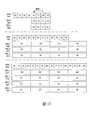
上方範例係顯示載入跨步2之執行。記憶體XB01包括其在記憶體中交替的兩個不同資料類型(X及Y)。提取之開始點係在Y0之開頭。於此範例中跨步為2。緊縮資料目的地暫存器0 XB03係儲存X類型之跨步資料元件而緊縮資料目的地暫存器1 XB05係儲存Y類型之跨步資料元件。The example above shows the execution of
中間範例係顯示載入跨步3之執行。記憶體XB07包括其在記憶體中交替的三個不同資料類型(X、Y、及Z)。提取之開始點係在X0之開頭。於此範例中跨步為3。緊縮資料目的地暫存器0 XB09係儲存X類型之跨步資料元件,緊縮資料目的地暫存器1 XB11係儲存Y類型之跨步資料元件,而緊縮資料目的地暫存器2 XB13係儲存Z類型之跨步資料元件。The middle example shows the execution of
底部範例係顯示載入跨步4之執行。記憶體XB15包括其在記憶體中交替的四個不同資料類型(X、Y、Z、及W)。提取之開始點係在W0之開頭。於此範例中跨步為4。緊縮資料目的地暫存器0 XB17係儲存W類型之跨步資料元件,緊縮資料目的地暫存器1 XB19係儲存X類型之跨步資料元件,緊縮資料目的地暫存器2 XB21係儲存Y類型之跨步資料元件,而緊縮資料目的地暫存器3 XB23係儲存Z類型之跨步資料元件。The bottom example shows the execution of
針對載入跨步#指令之格式的實施例為載入跨步#{B/W/D/Q}DSTREG,MEMORY。於某些實施例中,載入跨步#{B/W/D/Q}為該指令之運算碼。#係指示跨步值以及欲提取之資料類型的數目。B/W/D/Q係指示來源/目的地之資料元件大小為位元組、字元、雙字元、及四字元。DSTREG為開始緊縮資料目的地暫存器運算元。記憶體為欲開始提取之開始點的位址。An example of the format of the load stride# instruction is to load stride#{B/W/D/Q}DSTREG,MEMORY. In some embodiments, load step #{B/W/D/Q} is the operation code of the instruction. # Indicates the stride value and the number of data types to be extracted. B/W/D/Q indicates the source/destination data element size is byte, character, double character, and four character. DSTREG is an operand of the destination register to start compacting data. The memory is the address of the starting point to start fetching.
於某些實施例中,載入跨步#指令包括寫入遮蔽暫存器運算元。寫入遮蔽被用以條件性地控制每元件操作及結果之更新。根據該實施方式,寫入遮蔽係使用合併或歸零遮蔽。以述詞(寫入遮蔽、寫入遮蔽、或k暫存器)運算元所編碼之指令係使用該運算元以條件性地控制每元件計算操作及結果之更新至目的地運算元。述詞運算元已知為操作遮蔽(寫入遮蔽)暫存器。操作遮蔽為一組大小MAX_KL(64位元)之八個架構暫存器。注意:從此組8個架構暫存器,僅有k1至k7可被定址為述詞運算元。k0可被使用為一般來源或目的地但無法被編碼為述詞運算元。亦注意:述詞運算元可被用以致能針對具有記憶體運算元(來源或目的地)之某些指令的記憶體錯誤抑制。當作述詞運算元,操作遮蔽暫存器含有一位元以管理該操作/更新至向量暫存器之資料元件。通常,操作遮蔽暫存器可支援具有以下元件大小之指令:單精確度浮點(float32)、整數雙字元(int32)、雙精確度浮點(float64)、整數四字元(int64)。操作遮蔽暫存器之長度(MAX_KL)足以處置高達具有每元件一位元之64元件(亦即,64位元)。針對既定向量長度,各指令僅存取根據其資料類型所需要的最低有效遮蔽位元之數目。操作遮蔽暫存器以每元件粒度影響指令。因此,各資料元件之任何數字或非數字操作以及對於目的地運算元之中間結果的每元件更新被闡述於操作遮蔽暫存器之相應位元上。於大部分實施例中,作用為述詞運算元之操作遮蔽係遵循以下性質:1)假如相應操作遮蔽位元未被設定則該指令之操作不被履行於一元件(此暗示無例外或違反可由對於遮蔽掉元件之操作所造成,而因此,無例外旗標由於遮蔽掉操作而被更新);2)假如相應寫入遮蔽位元未被設定則目的地元件不被更新以該操作之結果。取而代之,目的地元件值需被保存(合併-遮蔽)或者其需被歸零掉(歸零-遮蔽);3)針對具有記憶體運算元之某些指令,記憶體錯誤被抑制於具有0之遮蔽位元的元件。注意:此特徵係提供多樣建構以實施控制流程斷定,因為有效遮蔽係提供針對向量暫存器目的地之合併行為。替代地,遮蔽可被用於歸零以取代合併,以致其遮蔽掉的元件被更新以0而取代保存舊值。歸零行為被提供以移除對於舊值之暗示依存性,當其不需要時。In some embodiments, the load stride# instruction includes writing a masked register operand. The write mask is used to conditionally control the operation of each element and the update of the result. According to this embodiment, the write masking uses merge or zero-return masking. The instruction coded with the predicate (write mask, write mask, or k register) operand uses the operand to conditionally control the calculation operation of each element and the update of the result to the destination operand. The predicate operand is known as the operation mask (write mask) register. The operation mask is a set of eight frame registers of MAX_KL (64 bits). Note: From this group of 8 architecture registers, only k1 to k7 can be addressed as predicate operands. k0 can be used as a general source or destination but cannot be encoded as a predicate operand. Also note that predicate operands can be used to enable memory error suppression for certain instructions with memory operands (source or destination). As a predicate operand, the operation mask register contains one bit to manage the operation/update to the data element of the vector register. Generally, the operation mask register can support instructions with the following component sizes: single-precision floating point(float32), integer double character (int32), double precision floating point (float64), integer four character (int64). The length of the operation mask register (MAX_KL) is sufficient to handle up to 64 elements with one bit per element (ie, 64 bits). For a given vector length, each instruction only accesses the number of least effective masking bits required by its data type. The operation mask register affects instructions at a per-element granularity. Therefore, any digital or non-digital operation of each data element and each element update of the intermediate result of the destination operand is described on the corresponding bit of the operation mask register. In most embodiments, the operation mask that acts as a predicate operand follows the following properties: 1) If the corresponding operation mask bit is not set, the operation of the instruction is not performed on a component (this implies no exception or violation) It can be caused by the operation of masking the component, and therefore, the no exception flag is updated due to the masking operation); 2) If the corresponding write mask bit is not set, the destination component will not be updated as the result of the operation . Instead, the destination component value needs to be saved (merge-mask) or it needs to be zeroed out (zero-mask); 3) For some instructions with memory operands, memory errors are suppressed to those with 0 Component that masks bits. Note: This feature provides multiple constructions to implement control flow determination, because effective masking provides merge behavior for the destination of the vector register. Alternatively, masking can be used to reset to zero instead of merging, so that the masked components are updated with 0 instead of saving the old value. The zeroing behavior is provided to remove the implied dependency on the old value when it is not needed.
於實施例中,該些指令之編碼包括比例-指標-基礎(SIB)類型記憶體定址運算元,其係間接地識別記憶體中之數個索引的目的地位置。於一實施例中,SIB類型記憶體運算元包括編碼識別基礎位址暫存器。基礎位址暫存器之內容係表示記憶體中之基礎位址,記憶體中之特定目的地位置的位址係從該基礎位址所計算。例如,基礎位址為針對延伸向量指令之潛在目的地位置的區塊中之第一位置的位址。於一實施例中,SIB類型記憶體運算元包括編碼識別指標暫存器。指標暫存器之各元件係指明可用以計算(從基礎位址)潛在目的地位置之區塊內的個別目的地位置之位址的指標或偏移值。於一實施例中,SIB類型記憶體運算元包括編碼指明比例因數以供應用至各指標值,當計算個別目的地位址時。例如,假如四之比例因數值被編碼以SIB類型記憶體運算元,則從指標暫存器之元件所獲得的各指標值被乘以四並接著加至基礎位址以計算目的地位址。In the embodiment, the codes of these instructions include scale-index-basis (SIB) type memory address operands, which indirectly identify the memoryThe destination location of several indexes in. In one embodiment, the SIB type memory operand includes a code recognition base address register. The content of the base address register represents the base address in the memory, and the address of a specific destination location in the memory is calculated from the base address. For example, the base address is the address of the first location in the block for the potential destination location of the extended vector instruction. In one embodiment, the SIB type memory operand includes a coded identification index register. Each element of the index register indicates the index or offset value that can be used to calculate (from the base address) the address of the individual destination location in the block of potential destination locations. In one embodiment, the SIB-type memory operand includes a code indicating a scale factor to be applied to each index value when calculating individual destination addresses. For example, if the scale factor value of four is coded with SIB type memory operands, each index value obtained from the element of the index register is multiplied by four and then added to the base address to calculate the destination address.
於一實施例中,形式vm32{x,y,z}之SIB類型記憶體運算元係識別其使用SIB類型記憶體定址所指明之記憶體運算元的向量陣列。於此範例中,記憶體位址之陣列係使用共同基礎暫存器、恆定比例因數、及向量指標暫存器(含有個別元件)來指明,其各為32位元指標值。向量指標暫存器可為XMM暫存器(vm32x)、YMM暫存器(vm32y)、或ZMM暫存器(vm32z)。於另一實施例中,形式vm64{x,y,z}之SIB類型記憶體運算元係識別其使用SIB類型記憶體定址所指明之記憶體運算元的向量陣列。於此範例中,記憶體位址之陣列係使用共同基礎暫存器、恆定比例因數、及向量指標暫存器(含有個別元件)來指明,其各為64位元指標值。向量指標暫存器可為XMM暫存器(vm64x)、YMM暫存器(vm64y)或ZMM暫存器(vm64z)。In one embodiment, the SIB type memory operand of the form vm32{x,y,z} recognizes the vector array of the memory operand specified by the SIB type memory addressing. In this example, the array of memory addresses is specified using a common base register, a constant scale factor, and a vector index register (including individual components), each of which is a 32-bit index value. The vector index register can be an XMM register (vm32x), a YMM register (vm32y), or a ZMM register (vm32z). In another embodiment, the SIB type memory operand of the form vm64{x,y,z} recognizes the vector array of the memory operand specified by the SIB type memory addressing. In this example, the array of memory addresses uses common base temporary storage, Constant scale factor, and vector index register (contains individual components) to indicate, each of which is a 64-bit index value. The vector index register can be an XMM register (vm64x), a YMM register (vm64y) or a ZMM register (vm64z).
圖3闡明載入跨步#指令之實施例,包括針對運算碼301、目的地運算元303、來源記憶體運算元305、及(於某些實施例中)寫入遮蔽運算元307之值。FIG. 3 illustrates an embodiment of the load stride# instruction, including writing the value of the
圖4闡明由用以處理載入跨步#指令之處理器所履行的方法之實施例。Figure 4 illustrates an embodiment of a method performed by a processor for processing load stride# instructions.
於401,指令被提取。例如,載入跨步#指令被提取。載入跨步#指令包括運算碼、記憶體來源位址、及緊縮資料目的地暫存器運算元,如以上所詳述。於某些實施例中,載入跨步#指令包括寫入遮蔽運算元。於某些實施例中,該指令被提取自指令快取。At 401, the instruction is fetched. For example, the load stride# instruction is fetched. The load step # instruction includes the operation code, the memory source address, and the compressed data destination register operand, as described in detail above. In some embodiments, the load stride# instruction includes writing a masked operand. In some embodiments, the instruction is fetched from the instruction cache.
提取的指令被解碼於403。例如,提取的載入跨步#指令係由解碼電路(諸如文中所詳述者)所解碼。The fetched instruction is decoded in 403. For example, the extracted load stride# instruction is decoded by a decoding circuit (such as those described in detail in the text).
與已解碼指令之來源運算元關聯的資料值被擷取於405。例如,來自記憶體之相連元件被存取,於來源位址開始。The data value associated with the source operand of the decoded instruction is retrieved at 405. For example, the connected component from the memory is accessed, starting at the source address.
於407,已解碼指令係由執行電路(硬體)所執行,諸如文中所詳述者。針對載入跨步#指令,該執行將從相連記憶體(於該指令之來源位址開始)提取#類型之資料元件;以及針對各類型,載入其專屬於該類型之緊縮資料暫存器中的已提取資料元件。At 407, the decoded instruction is executed by the execution circuit (hardware), such as those described in detail in the text. For the load step # command, the execution will extract the # type data element from the connected memory (starting from the source address of the command); and for each type, load its own compact data register for that type The extracted data component in.
於某些實施例中,該指令被確定或止用於409。In some embodiments, this instruction is confirmed or disabled for 409.
圖5闡明由用以處理載入跨步#指令之處理器所履行的方法之執行部分的實施例。Figure 5 illustrates an embodiment of the execution part of a method performed by a processor for processing load stride# instructions.
於501,以位元組為單位之資料元件大小的判定被做出。此大小為由該指令除以8所界定的元件大小。At 501, the determination of the size of the data element in bytes is made. This size is the element size defined by the command divided by 8.
於503,目的地暫存器名稱/映圖被產生。於某些實施例中,此係由解碼電路所完成。於其他實施例中,暫存器重新命名硬體進行此動作。通常,目的地暫存器為連續數字,開始於該指令之目的地暫存器運算元。例如,當目的地暫存器運算元為ZMM2時,則針對載入跨步2,ZMM3為欲使用之下一目的地暫存器。At 503, the destination register name/map is generated. In some embodiments, this is done by a decoding circuit. In other embodiments, the register renames the hardware to perform this action. Usually, the destination register is a continuous number, starting with the destination register operand of the instruction. For example, when the operand of the destination register is ZMM2, for
於505,欲擷取之資料元件的最大數目之判定被做出。此大小為該目的地暫存器除以該元件大小(以位元為單位)之大小。At 505, the determination of the maximum number of data elements to be retrieved is made. This size is the size of the destination register divided by the size of the device (in bits).
於507,每資料類型之資料元件被提取。這些資料元件被提取自位置i*跨步*元件大小(以位元組為單位),開始於i=0而至i=資料元件之最大數目減一。於某些實施例中,寫入遮蔽被用以判定何者被寫入。At 507, data elements of each data type are extracted. These data elements are extracted from position i*stride* element size (in bytes), starting at i=0 and ending at i=maximum number of data elements minus one. In some embodiments, write masking is used to determine which is written.
圖6闡明針對載入跨步2之虛擬碼的實施例。FIG. 6 illustrates an embodiment for loading the virtual code of
圖7闡明針對載入跨步3之虛擬碼的實施例。FIG. 7 illustrates an embodiment for loading the virtual code of
圖8闡明針對載入跨步4之虛擬碼的實施例。FIG. 8 illustrates an embodiment for loading the virtual code of
圖9闡明用以處理儲存跨步#(storestride#)指令之硬體的實施例。所闡明的硬體通常為硬體處理器或核心之部分,諸如中央處理單元、加速器等等之部分。FIG. 9 illustrates an embodiment of the hardware used to process the storestride# instruction. The explained hardware is usually a part of a hardware processor or core, such as a central processing unit, an accelerator, and so on.
儲存跨步#指令係由解碼電路901所接收。例如,解碼電路901係從提取邏輯/電路接收此指令。儲存跨步#指令包括針對開始記憶體位置(目的地運算元)及開始緊縮目的地暫存器來源之欄位。該指令之運算碼中的#為跨步長度且為2、3、或4,並相應於將被儲存記憶體中之結構的資料元件類型之數目以及其以該開始緊縮目的地暫存器開始之來源緊縮資料暫存器之數目。指令格式之更詳細實施例將被詳述於後。解碼電路901將儲存跨步#指令解碼為一或更多操作。於某些實施例中,此解碼包括產生複數微操作以供由執行電路(諸如執行電路909)所履行。解碼電路901亦解碼指令前綴。The storage step # command is received by the
於某些實施例中,暫存器重新命名、暫存器配置、及/或排程電路903提供以下之一或更多者的功能:1)重新命名邏輯運算元值為實體運算元值(例如,於某些實施例中之暫存器別名表),2)配置狀態位元和旗標至已解碼指令,及3)從指令池排程已解碼指令以供執行於執行電路909上(例如,於某些實施例中使用保留站)。In some embodiments, the register renaming, register configuration, and/or
暫存器(暫存器檔)905及記憶體907將資料儲存為儲存跨步#指令之運算元,以供操作於執行電路909上。範例暫存器類型包括緊縮資料暫存器、通用暫存器、及浮點暫存器。The register (register file) 905 and the
執行電路909係執行已解碼的儲存跨步#指令以從#緊縮資料暫存器提取#類型之資料元件(其中#為2、3、或4),以及將那些資料元件交錯儲存入於來源記憶體位址開始之相連的記憶體。記憶體中之特定類型的資料元件被跨步以致其一類型之各資料元件係與相同類型之另一資料元件彼此分離#資料元件位置。此情況之範例被闡明。The
於某些實施例中,止用電路911係架構上地止用該指令。In some embodiments, the disable
圖10闡明儲存跨步#指令之執行的實施例。這些範例並非為了限制。欲提取之緊縮資料元件的數目及其大小係取決於指令編碼(資料元件大小)及目的地暫存器數。如此一來,不同數目的緊縮資料元件(諸如2、4、8、16、32、或64)可被提取。緊縮資料目的地暫存器大小包括64位元、128位元、256位元、及512位元。Figure 10 illustrates an embodiment of storing the execution of the step# instruction. These examples are not meant to be limiting. The number of compressed data elements to be extracted and their size depend on the command code (data element size) and the number of destination registers. In this way, different numbers of compressed data elements (such as 2, 4, 8, 16, 32, or 64) can be extracted. The size of the compressed data destination register includes 64-bit, 128-bit, 256-bit, and 512-bit.
上方範例係顯示儲存跨步2之執行。記憶體1001係儲存其在記憶體中交替的兩個不同資料類型(X及Y),於該指令之執行後。提取之開始點係在Y0之開頭。於此範例中跨步為2。緊縮資料目的地暫存器0 1003係儲存X類型之跨步資料元件而緊縮資料目的地暫存器1 1005係儲存Y類型之跨步資料元件。The example above shows the execution of
中間範例係顯示儲存跨步3之執行。記憶體1007係儲存其在記憶體中交替的三個不同資料類型(X、Y、及Z),於該指令之執行後。提取之開始點係在X0之開頭。於此範例中跨步為3。緊縮資料目的地暫存器0 1009係儲存X類型之跨步資料元件,緊縮資料目的地暫存器1 1011係儲存Y類型之跨步資料元件,而緊縮資料目的地暫存器2 1013係儲存Z類型之跨步資料元件。The middle example shows the execution of
底部範例係顯示儲存跨步4之執行。記憶體1015係儲存其在記憶體中交替的四個不同資料類型(X、Y、Z、及W),於該指令之執行後。提取之開始點係在W0之開頭。於此範例中跨步為4。緊縮資料目的地暫存器0 1017係儲存W類型之跨步資料元件,緊縮資料目的地暫存器1 1019係儲存X類型之跨步資料元件,緊縮資料目的地暫存器2 1021係儲存Y類型之跨步資料元件,而緊縮資料目的地暫存器3 1023係儲存Z類型之跨步資料元件。The bottom example shows the execution of
針對儲存跨步#指令之格式的實施例為儲存跨步#{B/W/D/Q}MEMORY,SRCREG。於某些實施例中,儲存跨步#{B/W/D/Q}為該指令之運算碼。#係指示跨步值以及欲提取之資料類型的數目。B/W/D/Q係指示來源/目的地之資料元件大小為位元組、字元、雙字元、及四字元。SRCREG為開始緊縮資料目的地暫存器運算元。記憶體為欲開始提取之開始點的位址。An example of the format of the storage step # instruction is to store step #{B/W/D/Q}MEMORY,SRCREG. In some embodiments, the storage step #{B/W/D/Q} is the operation code of the instruction. # Indicates the stride value and the number of data types to be extracted. B/W/D/Q indicates the source/destination data element size is byte, character, double character, and four character. SRCREG is an operand of the destination register to start compacting data. The memory is the address of the starting point to start fetching.
於某些實施例中,儲存跨步#指令包括寫入遮蔽暫存器運算元。寫入遮蔽被用以條件性地控制每元件操作及結果之更新。根據該實施方式,寫入遮蔽係使用合併或歸零遮蔽。以述詞(寫入遮蔽、寫入遮蔽、或k暫存器)運算元所編碼之指令係使用該運算元以條件性地控制每元件計算操作及結果之更新至目的地運算元。述詞運算元已知為操作遮蔽(寫入遮蔽)暫存器。操作遮蔽為一組大小MAX_KL(64位元)之八個架構暫存器。注意:從此組8個架構暫存器,僅有k1至k7可被定址為述詞運算元。k0可被使用為一般來源或目的地但無法被編碼為述詞運算元。亦注意:述詞運算元可被用以致能針對具有記憶體運算元(來源或目的地)之某些指令的記憶體錯誤抑制。當作述詞運算元,操作遮蔽暫存器含有一位元以管理該操作/更新至向量暫存器之資料元件。通常,操作遮蔽暫存器可支援具有以下元件大小之指令:單精確度浮點(float32)、整數雙字元(int32)、雙精確度浮點(float64)、整數四字元(int64)。操作遮蔽暫存器之長度(MAX_KL)足以處置高達具有每元件一位元之64元件(亦即,64位元)。針對既定向量長度,各指令僅存取根據其資料類型所需要的最低有效遮蔽位元之數目。操作遮蔽暫存器以每元件粒度影響指令。因此,各資料元件之任何數字或非數字操作以及對於目的地運算元之中間結果的每元件更新被闡述於操作遮蔽暫存器之相應位元上。於大部分實施例中,作用為述詞運算元之操作遮蔽係遵循以下性質:1)假如相應操作遮蔽位元未被設定則該指令之操作不被履行於一元件(此暗示無例外或違反可由對於遮蔽掉元件之操作所造成,而因此,無例外旗標由於遮蔽掉操作而被更新);2)假如相應寫入遮蔽位元未被設定則目的地元件不被更新以該操作之結果。取而代之,目的地元件值需被保存(合併-遮蔽)或者其需被歸零掉(歸零-遮蔽);3)針對具有記憶體運算元之某些指令,記憶體錯誤被抑制於具有0之遮蔽位元的元件。注意:此特徵係提供多樣建構以實施控制流程斷定,因為有效遮蔽係提供針對向量暫存器目的地之合併行為。替代地,遮蔽可被用於歸零以取代合併,以致其遮蔽掉的元件被更新以0而取代保存舊值。歸零行為被提供以移除對於舊值之暗示依存性,當其不需要時。In some embodiments, the store step# instruction includes writing a masked register operand. The write mask is used to conditionally control the operation of each element and the update of the result. According to this embodiment, the write masking uses merge or zero-return masking. The instruction coded with the predicate (write mask, write mask, or k register) operand uses the operand to conditionally control the calculation operation of each element and the update of the result to the destination operand. The predicate operand is known as the operation mask (write mask) register. The operation mask is a set of eight frame registers of MAX_KL (64 bits). Note: From this group of 8 architecture registers, only k1 to k7 can be addressed as predicate operands. k0Can be used as a general source or destination but cannot be encoded as a predicate operand. Also note that predicate operands can be used to enable memory error suppression for certain instructions with memory operands (source or destination). As a predicate operand, the operation mask register contains one bit to manage the operation/update to the data element of the vector register. Generally, the operation mask register can support instructions with the following component sizes: single-precision floating point (float32), integer double-character (int32), double-precision floating point (float64), integer four-character (int64) . The length of the operation mask register (MAX_KL) is sufficient to handle up to 64 elements with one bit per element (ie, 64 bits). For a given vector length, each instruction only accesses the number of least effective masking bits required by its data type. The operation mask register affects instructions at a per-element granularity. Therefore, any digital or non-digital operation of each data element and each element update of the intermediate result of the destination operand is described on the corresponding bit of the operation mask register. In most embodiments, the operation mask that acts as a predicate operand follows the following properties: 1) If the corresponding operation mask bit is not set, the operation of the instruction is not performed on a component (this implies no exception or violation) It can be caused by the operation of masking the component, and therefore, the no exception flag is updated due to the masking operation); 2) If the corresponding write mask bit is not set, the destination component will not be updated as the result of the operation . Instead, the destination component value needs to be saved (merge-mask) or it needs to be zeroed out (zero-mask); 3) For some instructions with memory operands, memory errors are suppressed to those with 0 Component that masks bits. Note: This feature provides a variety of constructions to implement control flow determination, because effective shielding improvesFor the merge behavior of the destination of the vector register. Alternatively, masking can be used to reset to zero instead of merging, so that the masked components are updated with 0 instead of saving the old value. The zeroing behavior is provided to remove the implied dependency on the old value when it is not needed.
於實施例中,該些指令之編碼包括比例-指標-基礎(SIB)類型記憶體定址運算元,其係間接地識別記憶體中之數個索引的目的地位置。於一實施例中,SIB類型記憶體運算元包括編碼識別基礎位址暫存器。基礎位址暫存器之內容係表示記憶體中之基礎位址,記憶體中之特定目的地位置的位址係從該基礎位址所計算。例如,基礎位址為針對延伸向量指令之潛在目的地位置的區塊中之第一位置的位址。於一實施例中,SIB類型記憶體運算元包括編碼識別指標暫存器。指標暫存器之各元件係指明可用以計算(從基礎位址)潛在目的地位置之區塊內的個別目的地位置之位址的指標或偏移值。於一實施例中,SIB類型記憶體運算元包括編碼指明比例因數以供應用至各指標值,當計算個別目的地位址時。例如,假如四之比例因數值被編碼以SIB類型記憶體運算元,則從指標暫存器之元件所獲得的各指標值被乘以四並接著加至基礎位址以計算目的地位址。In an embodiment, the codes of the commands include scale-index-based (SIB) type memory addressing operands, which indirectly identify the destination locations of several indexes in the memory. In one embodiment, the SIB type memory operand includes a code recognition base address register. The content of the base address register represents the base address in the memory, and the address of a specific destination location in the memory is calculated from the base address. For example, the base address is the address of the first location in the block for the potential destination location of the extended vector instruction. In one embodiment, the SIB type memory operand includes a coded identification index register. Each element of the index register indicates the index or offset value that can be used to calculate (from the base address) the address of the individual destination location in the block of potential destination locations. In one embodiment, the SIB-type memory operand includes a code indicating a scale factor to be applied to each index value when calculating individual destination addresses. For example, if the scale factor value of four is coded with SIB type memory operands, each index value obtained from the element of the index register is multiplied by four and then added to the base address to calculate the destination address.
於一實施例中,形式vm32{x,y,z}之SIB類型記憶體運算元係識別其使用SIB類型記憶體定址所指明之記憶體運算元的向量陣列。於此範例中,記憶體位址之陣列係使用共同基礎暫存器、恆定比例因數、及向量指標暫存器(含有個別元件)來指明,其各為32位元指標值。向量指標暫存器可為XMM暫存器(vm32x)、YMM暫存器(vm32y)、或ZMM暫存器(vm32z)。於另一實施例中,形式vm64{x,y,z}之SIB類型記憶體運算元係識別其使用SIB類型記憶體定址所指明之記憶體運算元的向量陣列。於此範例中,記憶體位址之陣列係使用共同基礎暫存器、恆定比例因數、及向量指標暫存器(含有個別元件)來指明,其各為64位元指標值。向量指標暫存器可為XMM暫存器(vm64x)、YMM暫存器(vm64y)或ZMM暫存器(vm64z)。In one embodiment, the SIB type memory operand of the form vm32{x,y,z} recognizes the vector array of the memory operand specified by the SIB type memory addressing. In this example, the array of memory addresses uses common base registers, constant scale factors, and vector index registers(Including individual components) to indicate that each is a 32-bit index value. The vector index register can be an XMM register (vm32x), a YMM register (vm32y), or a ZMM register (vm32z). In another embodiment, the SIB type memory operand of the form vm64{x,y,z} recognizes the vector array of the memory operand specified by the SIB type memory addressing. In this example, the array of memory addresses is specified using a common base register, a constant scale factor, and a vector index register (including individual components), each of which is a 64-bit index value. The vector index register can be an XMM register (vm64x), a YMM register (vm64y) or a ZMM register (vm64z).
圖11闡明儲存跨步#指令之實施例,包括針對運算碼1101、目的地記憶體位址運算元1103、開始來源暫存器運算元1105、及(於某些實施例中)寫入遮蔽運算元1107之值。Figure 11 illustrates an embodiment of the store step # instruction, including
圖12闡明由用以處理儲存跨步#指令之處理器所履行的方法之實施例。Figure 12 illustrates an embodiment of a method performed by a processor for processing store stride# instructions.
於1201,指令被提取。例如,儲存跨步#指令被提取。儲存跨步#指令包括運算碼、記憶體目的地位址、及緊縮資料來源暫存器運算元,如以上所詳述。於某些實施例中,儲存跨步#指令包括寫入遮蔽運算元。於某些實施例中,該指令被提取自指令快取。At 1201, the instruction was fetched. For example, the storage step # instruction is fetched. The storage step# command includes the operation code, the memory destination address, and the compressed data source register operand, as described in detail above. In some embodiments, the storing step# instruction includes writing a masked operand. In some embodiments, the instruction is fetched from the instruction cache.
提取的指令被解碼於1203。例如,提取的儲存跨步#指令係由解碼電路(諸如文中所詳述者)所解碼。The fetched instruction is decoded at 1203. For example, the extracted storage step# instruction is decoded by a decoding circuit (such as those described in detail in the text).
與已解碼指令之來源運算元關聯的資料值被擷取於1205。例如,來自記憶體之相連元件被存取,於來源位址開始。The data value associated with the source operand of the decoded instruction is retrieved in1205. For example, the connected component from the memory is accessed, starting at the source address.
於1207,已解碼指令係由執行電路(硬體)所執行,諸如文中所詳述者。針對儲存跨步#指令,該執行係用以從#緊縮資料暫存器提取#類型之資料元件(其中#為2、3、或4),以及將那些資料元件交錯儲存入於來源記憶體位址開始之相連的記憶體。At 1207, the decoded instruction is executed by the execution circuit (hardware), such as those detailed in the text. For the storage step# command, the execution is used to extract # type data elements from #compact data register (# is 2, 3, or 4), and interleave those data elements into the source memory address The memory connected to the beginning.
於某些實施例中,該指令被確定或止用於1209。In some embodiments, the instruction is determined or disabled for 1209.
圖13闡明由用以處理儲存跨步#指令之處理器所履行的方法之執行部分的實施例。FIG. 13 illustrates an embodiment of the execution part of the method performed by the processor for processing the store stride# instruction.
於1301,位元組中之資料元件大小的判定被做出。此大小為由該指令除以8所界定的元件大小。At 1301, the determination of the size of the data element in the byte is made. This size is the element size defined by the command divided by 8.
於1303,目的地暫存器名稱/映圖被產生。於某些實施例中,此係由解碼電路所完成。於其他實施例中,暫存器重新命名硬體進行此動作。通常,目的地暫存器為連續數字,開始於該指令之目的地暫存器運算元。例如,當目的地暫存器運算元為ZMM2時,則針對儲存跨步2,ZMM3為欲使用之下一目的地暫存器。At 1303, the destination register name/map is generated. In some embodiments, this is done by a decoding circuit. In other embodiments, the register renames the hardware to perform this action. Usually, the destination register is a continuous number, starting with the destination register operand of the instruction. For example, when the operand of the destination register is ZMM2, for
於1305,欲擷取之資料元件的最大數目之判定被做出。此大小為該目的地暫存器除以該元件大小(以位元為單位)之大小。At 1305, the determination of the maximum number of data elements to be retrieved is made. This size is the size of the destination register divided by the size of the device (in bits).
於1307,每資料類型之資料元件被交錯地儲存在記憶體中,於其由該指令所提供的位址上開始。這些資料元件被提取自位置i*跨步*元件大小(以位元組為單位),開始於i=0而至i=資料元件之最大數目減一。於某些實施例中,寫入遮蔽被用以判定何者被寫入。At 1307, the data elements of each data type are interleaved in the memory, starting at the address provided by the command. These data components are extracted from the position i * stride * component size (in bytes),Start at i=0 and go to i=the maximum number of data elements minus one. In some embodiments, write masking is used to determine which is written.
圖14闡明針對儲存跨步2之虛擬碼的實施例。FIG. 14 illustrates an embodiment for storing the virtual code of
圖15闡明針對儲存跨步3之虛擬碼的實施例。FIG. 15 illustrates an embodiment for storing the virtual code of
圖16闡明針對儲存跨步4之虛擬碼的實施例。FIG. 16 illustrates an embodiment for storing the virtual code of
以下圖形係詳述用以實施以上實施例之範例架構及系統。於某些實施例中,上述的一或更多硬體組件及/或指令被仿真如以下所詳述,或者被實施為軟體模組。The following figures detail an example architecture and system used to implement the above embodiments. In some embodiments, the one or more hardware components and/or commands described above are simulated as described in detail below, or implemented as software modules.
上述的指令之實施例所體現者可被體現於「一般向量友善指令格式」,其被詳述於下。於其他實施例中,此一格式未被利用而是另一指令格式被使用,然而,寫入遮蔽暫存器、各種資料轉變(拌合、廣播,等等)、定址等等之以下描述一般係可應用於上述指令之實施例的描述。此外,範例系統、架構、及管線被詳述於下。以上指令之實施例可被執行於此等系統、架構、及管線上,但不限定於那些細節。What is embodied in the above-mentioned instruction embodiment can be embodied in the "general vector-friendly instruction format", which is described in detail below. In other embodiments, this format is not used but another command format is used. However, the following descriptions of writing to the mask register, various data transformations (mixing, broadcasting, etc.), addressing, etc. are generally It is a description of the embodiments that can be applied to the above instructions. In addition, example systems, architectures, and pipelines are detailed below. The embodiments of the above instructions can be executed on these systems, architectures, and pipelines, but are not limited to those details.
指令集可包括一或更多指令格式。既定指令格式可界定各種欄位(例如,位元之數目、位元之位置)以指明(除了別的以外)待履行操作(例如,運算碼)以及將於其上履行操作之運算元及/或其他資料欄位(例如,遮罩)。一些指令格式係透過指令模板(或子格式)之定義而被進一步分解。例如,既定指令格式之指令模板可被定義以具有指令格式之欄位的不同子集(所包括的欄位通常係以相同順序,但至少某些具有不同的位元位置,因為包括了較少的欄位)及/或被定義以具有不同地解讀之既定欄位。因此,ISA之各指令係使用既定指令格式(以及,假如被定義的話,以該指令格式之指令模板的既定一者)而被表達,並包括用以指明操作及運算元之欄位。例如,範例ADD指令具有特定運算碼及一指令格式,其包括用以指明該運算碼之運算碼欄位及用以選擇運算元(來源1/目的地及來源2)之運算元欄位;而於一指令串中之此ADD指令的發生將具有特定內容於其選擇特定運算元之運算元欄位中。被稱為先進向量延伸(AVX)(AVX1及AVX2)並使用向量延伸(VEX)編碼技術之一組SIMD延伸已被釋出及/或出版(例如,參見Intel® 64及IA-32架構軟體開發商手冊,2014年九月;及參見Intel®先進向量延伸編程參考,2014年十月)。The instruction set may include one or more instruction formats. The established command format can define various fields (for example, the number of bits, the position of bits) to specify (among other things) the operation to be performed (for example, operation code) and the operand on which the operation will be performed and/ Or other data fields (for example, mask). Some instruction formats are further decomposed through the definition of instruction templates (or sub-formats). For example, the command template of a given command format can be defined to have different subsets of the fields of the command format (the fields included are usually in the same order, but at least some have different bit positions, because(Includes fewer fields) and/or is defined to have a different interpretation of the established fields. Therefore, each instruction of the ISA is expressed using a predetermined instruction format (and, if defined, a predetermined one of the instruction template of the instruction format), and includes fields for specifying operations and operands. For example, the example ADD instruction has a specific opcode and an instruction format, which includes an opcode field for specifying the opcode and an opcode field for selecting operands (
文中所述之指令的實施例可被實施以不同的格式。此外,範例系統、架構、及管線被詳述於下。指令之實施例可被執行於此等系統、架構、及管線上,但不限定於那些細節。The embodiments of the instructions described herein can be implemented in different formats. In addition, example systems, architectures, and pipelines are detailed below. The embodiments of the instructions can be executed on these systems, architectures, and pipelines, but are not limited to those details.
向量友善指令格式是一種適於向量指令之指令格式(例如,有向量操作特定的某些欄位)。雖然實施例係描述其中向量和純量操作兩者均透過向量友善指令格式而被支援,但替代實施例僅使用具有向量友善指令格式之向量操作。The vector-friendly instruction format is an instruction format suitable for vector instructions (for example, there are certain fields specific to vector operations). Although the embodiment is described in which both vector and scalar operations are implemented through a vector-friendly instruction formatYes, but the alternative embodiment only uses vector operations with vector-friendly instruction formats.
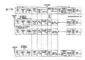
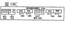
圖17A-17B為闡明一般性向量友善指令格式及其指令模板的方塊圖,依據本發明之實施例。圖17A為闡明一般性向量友善指令格式及其類別A指令模板的方塊圖,依據本發明之實施例;而圖17B為闡明一般性向量友善指令格式及其類別B指令模板的方塊圖,依據本發明之實施例。明確地,針對一般性向量友善指令格式1700係定義類別A及類別B指令模板,其兩者均包括無記憶體存取1705指令模板及記憶體存取1720指令模板。於向量友善指令格式之背景下術語「一般性」指的是不與任何特定指令集連結的指令格式。17A-17B are block diagrams illustrating the general vector-friendly instruction format and its instruction template, according to an embodiment of the present invention. Figure 17A is a block diagram illustrating the general vector-friendly instruction format and its category A instruction template, according to an embodiment of the present invention; and Figure 17B is a block diagram illustrating the general vector-friendly instruction format and its category B instruction template, according to this The embodiment of the invention. Specifically, for the general vector-friendly instruction format 1700, category A and category B instruction templates are defined, both of which include
雖然本發明之實施例將描述其中向量友善指令格式支援以下:具有32位元(4位元組)或64位元(8位元組)資料元件寬度(或大小)之64位元組向量運算元長度(或大小)(而因此,64位元組向量係由16雙字元大小的元件、或替代地8四字元大小的元件所組成);具有16位元(2位元組)或8位元(1位元組)資料元件寬度(或大小)之64位元組向量運算元長度(或大小);具有32位元(4位元組)、64位元(8位元組)、16位元(2位元組)、或8位元(1位元組)資料元件寬度(或大小)之32位元組向量運算元長度(或大小);及具有32位元(4位元組)、64位元(8位元組)、16位元(2位元組)、或8位元(1位元組)資料元件寬度(或大小)之16位元組向量運算元長度(或大小);但是替代實施例可支援具有更大、更小、或不同資料元件寬度(例如,128位元(16位元組)資料元件寬度)之更大、更小及/或不同的向量運算元大小(例如,256位元組向量運算元)。Although the embodiments of the present invention will describe that the vector-friendly instruction format supports the following: 64-byte vector operations with 32-bit (4-byte) or 64-bit (8-byte) data element width (or size) Element length (or size) (and therefore, a 64-bit vector is composed of 16 double-character sized elements, or alternatively 8 quad-character sized elements); it has 16 bits (2 bytes) or 8-bit (1 byte) data element width (or size) of 64-bit vector operand length (or size); 32-bit (4-byte), 64-bit (8-byte) , 16-bit (2-byte), or 8-bit (1-byte) data element width (or size) of 32-bit vector operand length (or size); and 32-bit (4 bits) Tuple), 64-bit (8-byte), 16-bit (2-byte), or 8-bit (1-byte) data element width (or largerSmaller) 16-byte vector operand length (or size); but alternative embodiments may support larger, smaller, or different data element widths (for example, 128-bit (16-byte) data element width) The larger, smaller, and/or different vector operand size (e.g., 256-byte vector operand).
圖17A中之類別A指令模板包括:1)於無記憶體存取1705指令模板內,顯示有無記憶體存取、全捨入控制類型操作1710指令模板及無記憶體存取、資料變換類型操作1715指令模板;以及2)於記憶體存取1720指令模板內,顯示有記憶體存取、暫時1725指令模板及記憶體存取、非暫時1730指令模板。圖17B中之類別B指令模板包括:1)於無記憶體存取1705指令模板內,顯示有無記憶體存取、寫入遮蔽控制、部分捨入控制類型操作1712指令模板及無記憶體存取、寫入遮蔽控制、v大小類型操作1717指令模板;以及2)於記憶體存取1720指令模板內,顯示有記憶體存取、寫入遮蔽控制1727指令模板。The category A command template in Figure 17A includes: 1) In the
一般性向量友善指令格式1700包括以下欄位,依圖17A-17B中所示之順序列出如下。The general vector-friendly instruction format 1700 includes the following fields, which are listed in the order shown in FIGS. 17A-17B.
格式欄位1740-此欄位中之一特定值(指令格式識別符值)係獨特地識別向量友善指令格式、以及因此在指令串中之向量友善指令格式的指令之發生。如此一來,此欄位是選擇性的,因為針對一僅具有一般性向量友善指令格式之指令集而言此欄位是不需要的。Format field 1740-A specific value in this field (command format identifier value) uniquely identifies the vector-friendly instruction format and therefore the occurrence of the vector-friendly instruction format in the instruction string. In this way, this field is optional, because it is not needed for an instruction set that only has a general vector-friendly instruction format.
基礎操作欄位1742-其內容係分辨不同的基礎操作。The basic operation field 1742-its content is to distinguish different basic operations.
暫存器指標欄位1744-其內容(直接地或透過位址產生)係指明來源及目的地運算元之位置,假設其係於暫存器中或記憶體中。這些包括足夠數目的位元以從PxQ(例如,32x512,16x128,32x1024,64x1024)暫存器檔選擇N暫存器。雖然於一實施例中N可高達三個來源及一個目的地暫存器,但是替代實施例可支援更多或更少的來源及目的地暫存器(例如,可支援高達兩個來源,其中這些來源之一亦作用為目的地;可支援高達三個來源,其中這些來源之一亦作用為目的地;可支援高達兩個來源及一個目的地)。The register index field 1744-its content (generated directly or by address) indicates the location of the source and destination operands, assuming it is in the register or memory. These include a sufficient number of bits to select the N register from the PxQ (for example, 32x512, 16x128, 32x1024, 64x1024) register file. Although N can be up to three sources and one destination register in one embodiment, alternative embodiments can support more or fewer source and destination registers (for example, up to two sources can be supported, where One of these sources also functions as a destination; up to three sources can be supported, of which one of these sources also functions as a destination; up to two sources and one destination can be supported).
修飾符欄位1746-其內容係從不指明記憶體存取之那些指令分辨出其指明記憶體存取之一般性向量指令格式的指令之發生,亦即,介於無記憶體存取1705指令模板與記憶體存取1720指令模板之間。記憶體存取操作係讀取及/或寫入至記憶體階層(於使用暫存器中之值以指明來源及/或目的地位址之某些情況下),而非記憶體存取操作則不會(例如,來源及目的地為暫存器)。雖然於一實施例中此欄位亦於三個不同方式之間選擇以履行記憶體位址計算,但是替代實施例可支援更多、更少、或不同方式以履行記憶體位址計算。The modifier field 1746-its content is to distinguish the occurrence of instructions in the general vector instruction format that specify memory access from those instructions that do not specify memory access, that is, between 1705 instructions without memory access Between the template and the
擴增操作欄位1750-其內容係分辨多種不同操作之哪一個將被履行,除了基礎操作之外。此欄位是背景特定的。於本發明之一實施例中,此欄位被劃分為類別欄位1768、α欄位1752、及β欄位1754。擴增操作欄位1750容許操作之共同群組將被履行以單指令而非2、3、或4指令。Augment operation field 1750-its content is to distinguish which of a variety of different operations will be performed, except for the basic operation. This field is background specificof. In an embodiment of the present invention, this field is divided into a
比例欄位1760-其內容容許指標欄位之內容的定標,以供記憶體位址產生(例如,以供其使用2比例*指標+基礎之位址產生)。
置換欄位1762A-其內容被使用為記憶體位址產生之部分(例如,以供其使用2比例*指標+基礎+置換之位址產生)。
置換因數欄位1762B(注意:直接在置換因數欄位1762B上方之置換欄位1762A的並列指示一者或另一者被使用)-其內容被使用為位址產生之部分;其指明將被記憶體存取之大小(N)所定標的置換因數-其中N為記憶體存取中之位元組數目(例如,以供其使用2比例*指標+基礎+定標置換之位址產生)。冗餘低階位元被忽略而因此,置換因數欄位之內容被乘以記憶體運算元總大小(N)來產生最終置換以供使用於計算有效位址。N之值係在運作時間由處理器硬體所判定,根據全運算碼欄位1774(稍後描述於文中)及資料調處欄位1754C。置換欄位1762A及置換因數欄位1762B是選擇性的,因為其未被使用於無記憶體存取1705指令模板及/或不同的實施例可實施該兩欄位之僅一者或者無任何。
資料元件寬度欄位1764-其內容係分辨數個資料元件之哪一個將被使用(於針對所有指令之某些實施例中;於針對僅某些指令之其他實施例中)。此欄位是選擇性的,在於其假如僅有一資料元件寬度被支援及/或資料元件寬度係使用運算碼之某形態而被支援則此欄位是不需要的。Data element width field 1764-its content distinguishes several data elementsWhich of the files will be used (in certain embodiments for all instructions; in other embodiments for only certain instructions). This field is optional, in that it is not needed if only one data element width is supported and/or the data element width is supported by a certain form of operation code.
寫入遮蔽欄位1770-其內容係根據每資料元件位置以控制其目的地向量運算元中之資料元件位置是否反映基礎操作及擴增操作之結果。類別A指令模板支援合併-寫入遮蔽,而類別B指令模板支援合併-及歸零-寫入遮蔽兩者。當合併時,向量遮蔽容許目的地中之任何組的元件被保護自任何操作之執行期間(由基礎操作及擴增操作所指明)的更新;於另一實施例中,保留其中相應遮蔽位元具有0之目的地的各元件之舊值。反之,當歸零時,向量遮蔽容許目的地中之任何組的元件被歸零於任何操作之執行期間(由基礎操作及擴增操作所指明);於一實施例中,當相應遮蔽位元具有0值時則目的地之一元件被設為0。此功能之子集是其控制被履行之操作的向量長度(亦即,被修飾之元件的範圍,從第一者至最後者)的能力;然而,其被修飾之元件不需要是連續的。因此,寫入遮蔽欄位1770容許部分向量操作,包括載入、儲存、運算、邏輯,等等。雖然本發明之實施例係描述其中寫入遮蔽欄位1770之內容選擇其含有待使用之寫入遮蔽的數個寫入遮蔽暫存器之一(而因此寫入遮蔽欄位1770之內容間接地識別其遮蔽將被履行),但是替代實施例取代地或者額外地容許寫入遮蔽欄位1770之內容直接地指明其遮蔽將被履行。Write the masked field 1770-its content is based on the position of each data element to control whether the data element position in the destination vector operand reflects the result of the basic operation and the augmentation operation. The class A command template supports merge-write masking, and the class B command template supports both merge-and zero-write masking. When merging, vector shadowing allows elements of any group in the destination to be protected from updates during the execution of any operation (specified by the basic operation and augmentation operation); in another embodiment, the corresponding shadowing bits are retained The old value of each component with a destination of 0. Conversely, when resetting to zero, vector shadowing allows elements of any group in the destination to be zeroed during the execution of any operation (specified by the basic operation and the amplification operation); in one embodiment, when the corresponding shadowing bit has When the value is 0, one of the components of the destination is set to 0. A subset of this function is its ability to control the length of the vector of the operation being performed (that is, the range of modified elements, from the first to the last); however, the modified elements need not be continuous. Therefore, the
即刻欄位1772-其內容容許即刻之指明。此欄位是選擇性的,由於此欄位存在於其不支援即刻之一般性向量友善格式的實施方式中且此欄位不存在於其不使用即刻之指令中。Immediate field 1772-its content allows immediate specification. This field is optional, because this field exists in the implementation that does not support the immediate general vector-friendly format and this field does not exist in the command without immediate use.
類別欄位1768-其內容分辨於不同類別的指令之間。參考圖17A-B,此欄位之內容選擇於類別A與類別B指令之間。於圖17A-B中,圓化角落的方形被用以指示一特定值存在於一欄位中(例如,針對類別欄位1768之類別A 1768A及類別B 1768B,個別地於圖17A-B中)。Category field 1768-its content is distinguished between commands of different categories. Referring to Figure 17A-B, the content of this field is selected between the category A and category B commands. In Figures 17A-B, the squares with rounded corners are used to indicate that a specific value exists in a field (for example,
於類別A之非記憶體存取1705指令模板的情況下,α欄位1752被解讀為RS欄位1752A,其內容係分辨不同擴增操作類型之哪一個將被履行(例如,捨入1752A.1及資料變換1752A.2被個別地指明給無記憶體存取、捨入類型操作1710及無記憶體存取、資料變換類型操作1715指令模板),而β欄位1754係分辨該些指明類型的操作之哪個將被履行。於無記憶體存取1705指令模板中,比例欄位1760、置換欄位1762A、及置換比例欄位1762B不存在。In the case of a
於無記憶體存取全捨入類型操作1710指令模板中,β欄位1754被解讀為捨入控制欄位1754A,其內容係提供靜態捨入。雖然於本發明之所述實施例中,捨入控制欄位1754A包括抑制所有浮點例外(SAE)欄位1756及捨入操作控制欄位1758,但替代實施例可支援可將這兩個觀念均編碼入相同欄位或僅具有這些觀念/欄位之一者或另一者(例如,可僅具有捨入操作控制欄位1758)。In the non-memory access full rounding type operation 1710 command template, the
SAE欄位1756-其內容係分辨是否除能例外事件報告;當SAE欄位1756之內容指示抑制被致能時,則一既定指令不報告任何種類的浮點例外旗標且不引發任何浮點例外處置器。The content of
捨入操作控制欄位1758-其內容係分辨一群捨入操作之哪一個將被履行(例如向上捨入、向下捨入、朝零捨入及捨入至最接近)。因此,捨入操作控制欄位1758容許以每指令為基之捨入模式的改變。於本發明之一實施例中,其中處理器包括一用以指明捨入模式之控制暫存器,捨入操作控制欄位1750之內容係撤銷該暫存器值。Rounding operation control field 1758-its content is to distinguish which of a group of rounding operations will be performed (for example, round up, round down, round toward zero, and round to nearest). Therefore, the rounding operation control field 1758 allows the change of the rounding mode on a per-command basis. In an embodiment of the present invention, the processor includes a control register for specifying the rounding mode, and the content of the rounding operation control field 1750 is to cancel the register value.
於無記憶體存取資料變換類型操作1715指令模板中,β欄位1754被解讀為資料變換欄位1754B,其內容係分辨數個資料變換之哪一個將被履行(例如,無資料變換、拌合、廣播)。In the non-memory access data conversion type operation 1715 command template, the
於類別A之記憶體存取1720指令模板的情況下,α欄位1752被解讀為逐出暗示欄位1752B,其內容係分辨逐出暗示之哪一個將被使用(於圖17A中,暫時1752B.1及非暫時1752B.2被個別地指明給記憶體存取、暫時1725指令模板及記憶體存取、非暫時1730指令模板),而β欄位1754被解讀為資料調處欄位1754C,其內容係分辨數個資料調處操作(亦已知為基元)之哪一個將被履行(例如,無調處;廣播;來源之向上轉換;及目的地之向下轉換)。記憶體存取1720指令模板包括比例欄位1760、及選擇性地置換欄位1762A或置換比例欄位1762B。In the case of
向量記憶體指令係履行向量載入自及向量儲存至記憶體,具有轉換支援。至於一般向量指令,向量記憶體指令係以資料元件式方式轉移資料自/至記憶體,以其被實際地轉移之元件由其被選為寫入遮蔽的向量遮蔽之內容所主宰。The vector memory instruction is to perform vector loading from and vector storage to memory, with conversion support. As for general vector instructions, vector memory instructions transfer data from/to memory in the form of data elements, and the elements that are actually transferred are dominated by the content of the vector mask that is selected as the write mask.
暫時資料為可能會夠早地被再使用以受惠自快取的資料。然而,此為一暗示,且不同的處理器可以不同的方式來實施,包括完全地忽略該暗示。Temporary data is data that may be reused early enough to benefit from the cache. However, this is a hint, and different processors can be implemented in different ways, including ignoring the hint altogether.
非暫時資料為不太可能會夠早地被再使用以受惠自第一階快取中之快取且應被給予逐出之既定優先權的資料。然而,此為一暗示,且不同的處理器可以不同的方式來實施,包括完全地忽略該暗示。Non-temporary data is data that is unlikely to be reused early enough to benefit from the cache in the first-level cache and should be given the established priority of eviction.However, this is a hint, and different processors can be implemented in different ways, including ignoring the hint altogether.
於類別B之指令模板的情況下,α欄位1752被解讀為寫入遮蔽控制(Z)欄位1752 C,其內容係分辨由寫入遮蔽欄位1770所控制的寫入遮蔽是否應為合併或歸零。In the case of the command template of category B, the
於類別B之非記憶體存取1705指令模板的情況下,β欄位1754之部分被解讀為RL欄位1757A,其內容係分辨不同擴增操作類型之哪一個將被履行(例如,捨入1757A.1及向量長度(VSIZE)1757A.2被個別地指明給無記憶體存取、寫入遮蔽控制、部分捨入控制類型操作1712指令模板及無記憶體存取、寫入遮蔽控制、VSIZE類型操作1717指令模板),而剩餘的β欄位1754係分辨該些指明類型的操作之哪個將被履行。於無記憶體存取1705指令模板中,比例欄位1760、置換欄位1762A、及置換比例欄位1762B不存在。In the case of the
於無記憶體存取中,寫入遮蔽控制、部分捨入控制類型操作1710指令模板、及剩餘的β欄位1754被解讀為捨入操作欄位1759A且例外事件報告被除能(既定指令則不報告任何種類的浮點例外旗標且不引發任何浮點例外處置器)。In memoryless access, write mask control, partial rounding control type operation 1710 command template, and the remaining
捨入操作控制欄位1759A-正如捨入操作控制欄位1758,其內容係分辨一群捨入操作之哪一個將被履行(例如向上捨入、向下捨入、朝零捨入及捨入至最接近)。因此,捨入操作控制欄位1759A容許以每指令為基之捨入模式的改變。於本發明之一實施例中,其中處理器包括一用以指明捨入模式之控制暫存器,捨入操作控制欄位1750之內容係撤銷該暫存器值。Rounding operation control field 1759A-just like the rounding operation control field 1758, its content is to distinguish which of a group of rounding operations will be performed (exampleSuch as round up, round down, round towards zero, and round to nearest). Therefore, the rounding operation control field 1759A allows the change of the rounding mode on a per-command basis. In an embodiment of the present invention, the processor includes a control register for specifying the rounding mode, and the content of the rounding operation control field 1750 is to cancel the register value.
於無記憶體存取、寫入遮蔽控制、VSIZE類型操作1717指令模板中,剩餘的β欄位1754被解讀為向量長度欄位1759B,其內容係分辨數個資料向量長度之哪一個將被履行(例如,128、256、或512位元組)。In the 1717 command template for non-memory access, write mask control, and VSIZE type operation, the remaining
於類別B之記憶體存取1720指令模板的情況下,β欄位1754之部分被解讀為廣播欄位1757B,其內容係分辨廣播類型資料調處操作是否將被履行,而剩餘的β欄位1754被解讀為向量長度欄位1759B。記憶體存取1720指令模板包括比例欄位1760、及選擇性地置換欄位1762A或置換比例欄位1762B。In the case of the
關於一般性向量友善指令格式1700,全運算碼欄位1774被顯示為包括格式欄位1740、基礎操作欄位1742、及資料元件寬度欄位1764。雖然一實施例被顯示為其中全運算碼欄位1774包括所有這些欄位,全運算碼欄位1774包括少於所有這些欄位在不支援其所有的實施例中。全運算碼欄位1774提供操作碼(運算碼)。Regarding the general vector-friendly instruction format 1700, the full operation code field 1774 is displayed as including a
擴增操作欄位1750、資料元件寬度欄位1764、及寫入遮蔽欄位1770容許這些特徵以每指令為基被指明以一般性向量友善指令格式。The augment operation field 1750, the data
寫入遮蔽欄位與資料元件寬度欄位之組合產生類型化的指令,在於其容許遮蔽根據不同資料元件寬度而被施加。The combination of the write mask field and the data element width field generates a typed command in that it allows the mask to be applied according to different data element widths.
類別A及類別B中所發現之各種指令模板在不同情況下是有利的。於本發明之某些實施例中,不同處理器或一處理器中之不同核心可支援僅類別A、僅類別B、或兩類別。例如,用於通用計算之高性能通用失序核心可支援僅類別B;主要用於圖形及/或科學(通量)計算之核心可支援僅類別A;及用於兩者之核心可支援兩者(當然,一種具有來自兩類別之模板和指令的某混合但非來自兩類別之所有模板和指令的核心是落入本發明之範圍內)。同時,單一處理器可包括多核心,其所有均支援相同的類別或者其中不同的核心支援不同的類別。例如,於一具有分離的圖形和通用核心之處理器中,主要用於圖形及/或科學計算的圖形核心之一可支援僅類別A;而通用核心之一或更多者可為高性能通用核心,其具有用於支援僅類別B之通用計算的失序執行和暫存器重新命名。不具有分離的圖形核心之另一處理器可包括支援類別A和類別B兩者之一或更多通用依序或失序核心。當然,來自一類別之特徵亦可被實施於另一類別中,在本發明之不同實施例中。以高階語言寫入之程式將被置入(例如,僅以時間編譯或靜態地編譯)多種不同的可執行形式,包括:1)僅具有由用於執行之處理器所支援的類別之指令的形式;或2)具有其使用所有類別之指令的不同組合所寫入之替代常式並具有控制流碼的形式,該控制流碼係根據由目前正執行該碼之處理器所支援的指令以選擇用來執行之常式。The various instruction templates found in category A and category B are advantageous in different situations. In some embodiments of the present invention, different processors or different cores in a processor can support only type A, only type B, or both types. For example, a high-performance general-purpose out-of-sequence core used for general-purpose computing can support only category B; a core mainly used for graphics and/or scientific (throughput) computing can support only category A; and a core used for both can support both (Of course, a core that has a certain mixture of templates and instructions from two categories but not all templates and instructions from both categories falls within the scope of the present invention). At the same time, a single processor may include multiple cores, all of which support the same category or different cores support different categories. For example, in a processor with separate graphics and general-purpose cores, one of the graphics cores mainly used for graphics and/or scientific computing can support only category A; and one or more of the general-purpose cores can be high-performance general-purpose The core, which has out-of-sequence execution and register renaming to support general calculations of only category B. Another processor that does not have a separate graphics core may include one or more general-purpose sequential or out-of-sequence cores that support both category A and category B. Of course, features from one category can also be implemented in another category, in different embodiments of the invention. Programs written in high-level languages will be placed (for example, compiled only in time or compiled statically) in a variety of different executable forms, including: 1) Those that only have instructions of the type supported by the processor used for execution Form; or 2) It has alternative routines written in different combinations of all types of instructionsIt also has the form of a control flow code, which is based on the instructions supported by the processor currently executing the code to select a routine for execution.
圖18為闡明範例特定向量友善指令格式的方塊圖,依據本發明之實施例。圖18顯示特定向量友善指令格式1800,其之特定在於其指明欄位之位置、大小、解讀、及順序,以及那些欄位之部分的值。特定向量友善指令格式1800可被用以延伸x86指令集,而因此某些欄位係類似於或相同於現存x86指令集及其延伸(例如,AVX)中所使用的那些。此格式保持與下列各者一致:具有延伸之現存x86指令集的前綴編碼欄位、真實運算碼位元組欄位、MOD R/M欄位、SIB欄位、置換欄位、及即刻欄位。闡明來自圖17之欄位投映入來自圖18之欄位。Figure 18 is a block diagram illustrating an example specific vector friendly instruction format, according to an embodiment of the present invention. FIG. 18 shows a specific vector-friendly instruction format 1800, which is specific in that it specifies the position, size, interpretation, and order of the fields, and the values of those fields. The specific vector-friendly instruction format 1800 can be used to extend the x86 instruction set, and therefore certain fields are similar or the same as those used in the existing x86 instruction set and its extensions (for example, AVX). This format remains consistent with the following: prefix code field with extended existing x86 instruction set, real operation code byte field, MOD R/M field, SIB field, replacement field, and immediate field . Clarify that the column from Figure 17 is projected into the column from Figure 18.
應理解:雖然本發明之實施例係參考為說明性目的之一般性向量友善指令格式1700的背景下之特定向量友善指令格式1800而描述,但除非其中有聲明否則本發明不限於特定向量友善指令格式1800。例如,一般性向量友善指令格式1700係考量各個欄位之多種可能大小,而特定向量友善指令格式1800被顯示為具有特定大小之欄位。舉特定例而言,雖然資料元件寬度欄位1764被闡明為特定向量友善指令格式1800之一位元欄位,但本發明未如此限制(亦即,一般性向量友善指令格式1700係考量資料元件寬度欄位1764之其他大小)。It should be understood that although the embodiments of the present invention are described with reference to the specific vector-friendly instruction format 1800 in the context of the general vector-friendly instruction format 1700 for illustrative purposes, the present invention is not limited to the specific vector-friendly instruction unless there is a statement therein. Format 1800. For example, the general vector-friendly instruction format 1700 considers multiple possible sizes of each field, and the specific vector-friendly instruction format 1800 is displayed as a field with a specific size. For a specific example, although the data
一般性向量友善指令格式1700包括以下欄位,依圖18A中所示之順序列出如下。The general vector-friendly instruction format 1700 includes the following fields, which are listed below in the order shown in FIG. 18A.
EVEX前綴(位元組0-3)1802被編碼以四位元組形式。The EVEX prefix (bytes 0-3) 1802 is coded in four-byte form.
格式欄位1740(EVEX位元組0,位元[7:0])-第一位元組(EVEX位元組0)為格式欄位1740且其含有0x62(用於分辨本發明之一實施例中的向量友善指令格式之獨特值)。Format field 1740 (
第二-第四位元組(EVEX位元組1-3)包括數個提供特定能力之位元欄位。The second-fourth byte (EVEX byte 1-3) includes several bit fields that provide specific capabilities.
REX欄位1805(EVEX位元組1,位元[7-5])-係包括:EVEX.R位元欄位(EVEX位元組1,位元[7]-R)、EVEX.X位元欄位(EVEX位元組1,位元[6]-X)、及1757BEX位元組1,位元[5]-B)。EVEX.R、EVEX.X、及EVEX.B位元欄位提供如相應VEX位元欄位之相同功能,且係使用1互補形式而被編碼,亦即,ZMM0被編碼為1111B,ZMM15被編碼為0000B。指令之其他欄位編碼該些暫存器指標之較低三位元如本技術中所已知者(rrr、xxx、及bbb),以致Rrrr、Xxxx、及Bbbb可藉由加入EVEX.R、EVEX.X、及EVEX.B而被形成。REX field 1805 (
REX'欄位1710-此為REX'欄位1710之第一部分且為EVER.R'位元欄位(EVEX位元組1,位元[4]-R’),其被用以編碼延伸的32暫存器集之上16個或下16個。於本發明之一實施例中,此位元(連同如以下所指示之其他者)被儲存以位元反轉格式來分辨(於眾所周知的x86 32-位元模式)自BOUND指令,其真實運算碼位元組為62,但於MOD R/M欄位(描述於下)中不接受MOD欄位中之11的值;本發明之替代實施例不以反轉格式儲存此及如下其他指示的位元。1之值被用以編碼下16暫存器。換言之,R'Rrrr係藉由結合EVEX.R'、EVEX.R、及來自其他欄位之其他RRR而被形成。REX' field 1710-This is the first part of REX' field 1710 and is the EVER.R' bit field (
運算碼映圖欄位1815(EVEX位元組1,位元[3:0]-mmmm)-其內容係編碼一暗示的領先運算碼位元組(0F、0F 38、或0F 3)。Operation code mapping field 1815 (
資料元件寬度欄位1764(EVEX位元組2,位元[7]-W)係由記號EVEX.W所表示。EVEX.W被用以界定資料類型(32位元資料元件或64位元資料元件)之粒度(大小)。The data element width field 1764 (
EVEX.vvvv 1820(EVEX位元組2,位元[6:3]-vvvv)-EVEX.vvv之角色可包括以下:1)EVEX.vvvv編碼其以反轉(1之補數)形式所指明的第一來源暫存器運算元且針對具有2或更多來源運算元為有效的;2)EVEX.vvvv針對某些向量位移編碼其以1之補數形式所指明的目的地暫存器運算元;或3)EVEX.vvvv未編碼任何運算元,該欄位被保留且應含有1111b。因此,EVEX.vvvv欄位1820係編碼其以反轉(1之補數)形式所儲存的第一來源暫存器指明符之4個低階位元。根據該指令,一額外的不同EVEX位元欄位被用以延伸指明符大小至32暫存器。EVEX.vvvv 1820 (
EVEX.U 1768類別欄位(EVEX位元組2,位元[2]-U)-假如EVEX.U=0,則其指示類別A或EVEX.U0;假如EVEX.U=1,則其指示類別B或EVEX.U1。
前綴編碼欄位1825(EVEX位元組2,位元[1:0]-pp)提供額外位元給基礎操作欄位。除了提供針對EVEX前綴格式之舊有SSE指令的支援,此亦具有壓縮SIMD前綴之優點(不需要一位元組來表達SIMD前綴,EVEX前綴僅需要2位元)。於一實施例中,為了支援其使用以舊有格式及以EVEX前綴格式兩者之SIMD前綴(66H、F2H、F3H)的舊有SSE指令,這些舊有SIMD前綴被編碼為SIMD前綴編碼欄位;且在運作時間被延伸入舊有SIMD前綴,在其被提供至解碼器的PLA以前(以致PLA可執行這些舊有指令之舊有和EVEX格式兩者而無須修改)。雖然較少的指令可將EVEX前綴編碼欄位之內容直接地使用為運算碼延伸,但某些實施例係以類似方式延伸以符合一致性而容許不同的意義由這些舊有SIMD前綴來指明。替代實施例可重新設計PLA以支援2位元SIMD前綴編碼,而因此不需要延伸。The prefix code field 1825 (
α欄位1752(EVEX位元組3,位元[7]-EH;亦已知為EVEX.EH、EVEX.rs、EVEX.RL、EVEX.寫入遮蔽控制、及EVEX.N;亦闡明以α)-如先前所描述,此欄位是背景特定的。α field 1752 (
β欄位1754(EVEX位元組3,位元[6:4]-SSS,亦已知為EVEX.s2-0、EVEX.r2-0、EVEX.rr1、EVEX.LL0、EVEX.LLB;亦闡明以βββ)-如先前所描述,此欄位是背景特定的。β field 1754 (
REX'欄位1710-此為REX'欄位之剩餘部分且為EVER.V'位元欄位(EVEX位元組3,位元[3]-V’),其被用以編碼延伸的32暫存器集之上16個或下16個。此位元被儲存以位元反轉格式。1之值被用以編碼下16暫存器。換言之,V'VVVV係藉由結合EVEX.V'、EVEX.vvvv所形成。REX' field 1710-This is the remainder of the REX' field and is the EVER.V' bit field (
寫入遮蔽欄位1770(EVEX位元組3,位元[2:0]-kkk)-其內容係指明在如先前所述之寫入遮蔽暫存器中的暫存器之指數。於本發明之一實施例中,特定值EVEX.kkk=000具有一特殊行為,其係暗示無寫入遮蔽被用於特別指令(此可被實施以多種方式,包括使用其固線至所有各者之寫入遮蔽或者其旁路遮蔽硬體之硬體)。Write mask field 1770 (
真實運算碼欄位1830(位元組4)亦已知為運算碼位元組。運算碼之部分被指明於此欄位。The real operation code field 1830 (byte 4) is also known as the operation code byte group. The part of the operation code is indicated in this field.
MOD R/M欄位1840(位元組5)包括MOD欄位1842、Reg欄位1844、及R/M欄位1846。如先前所述MOD欄位1842之內容係分辨於記憶體存取與非記憶體存取操作之間。Reg欄位1844之角色可被概述為兩情況:編碼目的地暫存器運算元或來源暫存器運算元、或者被視為運算碼延伸而不被用以編碼任何指令運算元。R/M欄位1846之角色可包括以下:編碼其參考記憶體位址之指令運算元;或者編碼目的地暫存器運算元或來源暫存器運算元。MOD R/M field 1840 (byte 5) includes
比例、指標、基礎(SIB)位元組(位元組6)-如先前所述,比例欄位1750之內容被用於記憶體位址產生。SIB.xxx 1854及SIB.bbb 1856-這些欄位之內容先前已被參考針對暫存器指標Xxxx及Bbbb。Scale, Index, Base (SIB) byte (byte 6)-As mentioned earlier, the content of the scale field 1750 is used for memory address generation. SIB.xxx 1854 and SIB.bbb 1856-The contents of these fields have previously been referenced for register indicators Xxxx and Bbbb.
置換欄位1762A(位元組7-10)-當MOD欄位1842含有10時,位元組7-10為置換欄位1762A,且其工作如舊有32位元置換(disp32)之相同方式且工作以位元組粒度。
置換因數欄位1762B(位元組7)-當MOD欄位1842含有01時,位元組7為置換因數欄位1762B。此欄位之位置係相同於舊有x86指令集8位元置換(disp8)之位置,其工作以位元組粒度。因為disp8是符號延伸的,所以其可僅定址於-128與127位元組偏移之間;關於64位元組快取線,disp8係使用其可被設為僅四個真實可用值-128、-64、0及64之8位元;因為較大範圍經常是需要的,所以disp32被使用;然而,disp32需要4位元組。相對於disp8及disp32,置換因數欄位1762B為disp8之再解讀;當使用置換因數欄位1762B時,實際置換係由置換因數欄位之內容乘以記憶體運算元存取之大小(N)所判定。置換欄位之類型被稱為disp8*N。此係減少平均指令長度(用於置換欄位之單一位元組但具有更大的範圍)。此壓縮置換是基於假設其有效置換為記憶體存取之粒度的數倍,而因此,位址偏移之冗餘低階位元無須被編碼。換言之,置換因數欄位1762B取代舊有x86指令集8位元置換。因此,置換因數欄位1762B被編碼以如x86指令集8位元置換之相同方式(以致ModRM/SIB編碼規則並無改變),唯一例外是其disp8被超載至disp8*N。換言之,編碼規則或編碼長度沒有改變,但僅於藉由硬體之置換值的解讀(其需由記憶體運算元之大小來定標置換以獲得位元組式的位址偏移)。即刻欄位1772係操作如先前所述。
圖18B為闡明其組成全運算碼欄位1774之特定向量友善指令格式1800的欄位之方塊圖,依據本發明之一實施例。明確地,全運算碼欄位1774包括格式欄位1740、基礎操作欄位1742、及資料元件寬度(W)欄位1764。基礎操作欄位1742包括前綴編碼欄位1825、運算碼映圖欄位1815、及真實運算碼欄位1830。FIG. 18B is a block diagram illustrating the fields of the specific vector-friendly instruction format 1800 which constitute the full operation code field 1774, according to an embodiment of the present invention. Specifically, the full operation code field 1774 includes a
圖18C為闡明其組成暫存器指標欄位1744之特定向量友善指令格式1800的欄位之方塊圖,依據本發明之一實施例。明確地,暫存器指標欄位1744包括REX欄位1805、REX'欄位1810、MODR/M.reg欄位1844、MODR/M.r/m欄位1846、VVVV欄位1820、xxx欄位1854、及bbb欄位1856。FIG. 18C is a block diagram illustrating the fields of the specific vector-friendly instruction format 1800 which constitute the
圖18D為闡明其組成擴增操作欄位1750之特定向量友善指令格式1800的欄位之方塊圖,依據本發明之一實施例。當類別(U)欄位1768含有0時,則其表示EVEX.U0(類別A 1768A);當其含有1時,則其表示EVEX.U1(類別B 1768B)。當U=0且MOD欄位1842含有11(表示無記憶體存取操作)時,則α欄位1752(EVEX位元組3,位元[7]-EH)被解讀為rs欄位1752A。當rs欄位1752A含有1(捨入1752A.1)時,則β欄位1754(EVEX位元組3,位元[6:4]-SSS)被解讀為捨入控制欄位1754A。捨入控制欄位1754A包括一位元SAE欄位1756及二位元捨入操作欄位1758。當rs欄位1752A含有0(資料變換1752A.2)時,則β欄位1754(EVEX位元組3,位元[6:4]-SSS)被解讀為三位元資料變換欄位1754B。當U=0且MOD欄位1842含有00、01、或10(表示記憶體存取操作)時,則α欄位1752(EVEX位元組3,位元[7]-EH)被解讀為逐出暗示(EH)欄位1752B且β欄位1754(EVEX位元組3,位元[6:4]-SSS)被解讀為三位元資料調處欄位1754C。FIG. 18D is a block diagram illustrating the fields of the specific vector-friendly instruction format 1800 constituting the augmentation operation field 1750, according to an embodiment of the present invention. When the category (U)
當U=1時,則α欄位1752(EVEX位元組3,位元[7]-EH)被解讀為寫入遮蔽控制(Z)欄位1752C。當U=1且MOD欄位1842含有11(表示無記憶體存取操作)時,則β欄位1754之部分(EVEX位元組3,位元[4]-S0)被解讀為RL欄位1757A;當其含有1(捨入1757A.1)時,則β欄位1754之剩餘部分(EVEX位元組3,位元[6-5]-S2-1)被解讀為捨入操作欄位1759A;而當RL欄位1757A含有0(VSIZE 1757.A2)時,則β欄位1754之剩餘部分(EVEX位元組3,位元[6-5]-S2-1)被解讀為向量長度欄位1759B(EVEX位元組3,位元[6-5]-L1-0)。當U=1且MOD欄位1842含有00、01、或10(表示記憶體存取操作)時,則β欄位1754(EVEX位元組3,位元[6:4]-SSS)被解讀為向量長度欄位1759B(EVEX位元組3,位元[6-5]-L1-0)及廣播欄位1757B(EVEX位元組3,位元[4]-B)。When U=1, the alpha field 1752 (
圖19為一暫存器架構1900之方塊圖,依據本發明之一實施例。於所示之實施例中,有32個向量暫存器1910,其為512位元寬;這些暫存器被稱為zmm0至zmm31。較低的16個zmm暫存器之較低階256位元被重疊於暫存器ymm0-16上。較低的16個zmm暫存器之較低階128位元(ymm暫存器之較低階128位元)被重疊於暫存器xmm0-15上。特定向量友善指令格式1800係操作於這些重疊的暫存器檔上,如以下表中所闡明。Figure 19 is a block diagram of a register architecture 1900 according to an embodiment of the present invention. In the illustrated embodiment, there are 32 vector registers 1910, which are 512 bits wide; these registers are called zmm0 to zmm31. The lower 256 bits of the lower 16 zmm registers are overlapped on the registers ymm0-16. The

換言之,向量長度欄位1759B於最大長度與一或更多其他較短長度之間選擇,其中每一此較短長度為前一長度之長度的一半;而無向量長度欄位1759B之指令模板係操作於最大長度上。此外,於一實施例中,特定向量友善指令格式1800之類別B指令模板係操作於緊縮或純量單/雙精確度浮點資料及緊縮或純量整數資料上。純量操作為履行於zmm/ymm/xmm暫存器中之最低階資料元件上的操作;較高階資料元件位置係根據實施例而被保留如其在該指令前之相同者或者被歸零。In other words, the
寫入遮蔽暫存器1915-於所示之實施例中,有8個寫入遮蔽暫存器(k0至k7),大小各為64位元。於替代實施例中,寫入遮蔽暫存器1915之大小為16位元。如先前所述,於本發明之一實施例中,向量遮蔽暫存器k0無法被使用為寫入遮蔽;當其通常將指示k0之編碼被用於寫入遮蔽時,其係選擇0xFFFF之固線寫入遮蔽,有效地除能該指令之寫入遮蔽。In the illustrated embodiment, there are 8 write mask registers (k0 to k7), each of which is 64 bits in size. In an alternative embodiment, the size of the write mask register 1915 is 16 bits. As mentioned earlier, in one embodiment of the present invention, the vector mask register k0 cannot be used for write masking; when it usually uses the code indicating k0 for write masking, it selects the fixed value of 0xFFFF. Line write mask, effectively disable the write mask of the command.
通用暫存器1925-於所示之實施例中,有十六個64位元通用暫存器,其係連同現存的x86定址模式來用以定址記憶體運算元。這些暫存器被參照以RAX、RBX、RCX、RDX、RBP、RSI、RDI、RSP、及R8至R15。The general purpose register 1925-In the illustrated embodiment, there are sixteen 64-bit general purpose registers, which are used in conjunction with the existing x86 addressing mode to address memory operands. These registers are referred to as RAX, RBX, RCX, RDX, RBP, RSI, RDI, RSP, and R8 to R15.
純量浮點堆疊暫存器檔(x87堆疊)1945,MMX緊縮整數平坦暫存器檔1950係別名於其上-於所示之實施例中,x87堆疊為用以使用x87指令集延伸而在32/64/80位元浮點資料上履行純量浮點操作之八元件堆疊;而MMX暫存器被用以履行操作在64位元緊縮整數資料上、及用以保持運算元以供介於MMX與XMM暫存器間所履行的某些操作。Scalar floating-point stacked register file (x87 stack) 1945, MMX compact integer flat register file 1950 is aliased on it-in the embodiment shown, the x87 stack is used to extend the x87 instruction set. The 8-element stack that performs scalar floating-point operations on 32/64/80-bit floating-point data; and the MMX register is used to perform operations on 64-bit compressed integer data and to hold the operands for introduction Some operations performed between MMX and XMM registers.
本發明之替代實施例可使用較寬或較窄的暫存器。此外,本發明之替代實施例可使用更多、更少、或不同的暫存器檔及暫存器。Alternative embodiments of the invention may use wider or narrower registers. In addition, alternative embodiments of the present invention may use more, fewer, or different registers and registers.
處理器核心可被實施以不同方式、用於不同目的、以及於不同處理器中。例如,此類核心之實施方式可包括:1)用於通用計算之通用依序核心;2)用於通用計算之高性能通用失序核心;3)主要用於圖形及/或科學(通量)計算之特殊用途核心。不同處理器之實施方式可包括:1)CPU,其包括用於通用計算之一或更多通用依序核心及/或用於通用計算之一或更多通用失序核心;及2)核心處理器,其包括主要用於圖形及/或科學(通量)之一或更多特殊用途核心。此等不同處理器導致不同的電腦系統架構,其可包括:1)在來自該CPU之分離晶片上的共處理器;2)在與CPU相同的封裝中之分離晶粒上的共處理器;3)在與CPU相同的晶粒上的共處理器(於該情況下,此一處理器有時被稱為特殊用途邏輯,諸如集成圖形及/或科學(通量)邏輯、或稱為特殊用途核心);及4)在一可包括於相同晶粒上之所述CPU(有時稱為應用程式核心或應用程式處理器)、上述共處理器、及額外功能的晶片上之系統。範例核心架構被描述於下,接續著範例處理器及電腦架構之描述。The processor core can be implemented in different ways, for different purposes, and in different processors. For example, implementations of such cores may include: 1) general-purpose sequential cores for general-purpose computing; 2) high-performance general-purpose out-of-sequence cores for general-purpose computing; 3) mainly for graphics and/or science (throughput) The special purpose core of computing. Implementations of different processors may include: 1) a CPU, which includes one or more general-purpose sequential cores for general-purpose computing and/or one or more general-purpose out-of-sequence cores for general-purpose computing; and 2) a core processor , Which includes one that is mainly used for graphics and/or science (flux) orMore special purpose cores. These different processors lead to different computer system architectures, which may include: 1) a co-processor on a separate chip from the CPU; 2) a co-processor on a separate die in the same package as the CPU; 3) A co-processor on the same die as the CPU (in this case, this processor is sometimes called special-purpose logic, such as integrated graphics and/or scientific (flux) logic, or special Application core); and 4) A system on a chip that can include the CPU (sometimes referred to as application core or application processor), the aforementioned co-processor, and additional functions on the same die. The example core architecture is described below, followed by the description of the example processor and computer architecture.
圖20A為闡明範例依序管線及範例暫存器重新命名、失序問題/執行管線兩者之方塊圖,依據本發明之實施例;圖20B為一方塊圖,其闡明將包括於依據本發明之實施例的處理器中之依序架構核心之範例實施例及範例暫存器重新命名、失序問題/執行架構核心兩者。圖20A-B中之實線方盒係闡明依序管線及依序核心,而虛線方盒之選擇性加入係闡明暫存器重新命名、失序問題/執行管線及核心。假設其依序形態為失序形態之子集,將描述失序形態。FIG. 20A is a block diagram illustrating both the example sequential pipeline and the example register renaming, out-of-sequence problem/execution pipeline, according to an embodiment of the present invention; FIG. 20B is a block diagram illustrating that it will be included in the example according to the present invention The example embodiment and the example register renaming of the sequential architecture core in the processor of the embodiment, the out-of-sequence problem/execution architecture core both. The solid square box in Figure 20A-B illustrates the sequential pipeline and sequential core, and the optional addition of the dotted square box illustrates the register renaming, out-of-sequence problem/execution pipeline and the core. Assuming that the sequential form is a subset of the out-of-order form, the out-of-order form will be described.
於圖20A中,處理器管線2000包括提取級2002、長度解碼級2004、解碼級2006、配置級2008、重新命名級2010、排程(亦已知為分派或發送)級2012、暫存器讀取/記憶體讀取級2014、執行級2016、寫入回/記憶體/寫入級2018、例外處置級2022、及確定級2024。In FIG. 20A, the
圖20B顯示處理器核心2090,其包括一耦合至執行引擎單元2050之前端單元2030,且兩者均耦合至記憶體單元2070。核心2090可為減少指令集計算(RISC)核心、複雜指令集計算(CISC)核心、極長指令字元(VLIW)核心、或者併合或替代核心類型。當作又另一種選擇,核心2090可為特殊用途核心,諸如(例如)網路或通訊核心、壓縮引擎、共處理器核心、通用計算圖形處理單元(GPGPU)核心、圖形核心,等等。FIG. 20B shows the
前端單元2030包括一分支預測單元2032,其係耦合至指令快取單元2034,其係耦合至指令變換後備緩衝(TLB)2036,其係耦合至指令提取單元2038,其係耦合至解碼單元2040。解碼單元2040(或解碼器)可解碼指令;並可將以下產生為輸出:一或更多微操作、微碼進入點、微指令、其他指令、或其他控制信號,其被解碼自(或者反應)、或被衍生自原始指令。解碼單元2040可使用各種不同的機制來實施。適當機制之範例包括(但不限定於)查找表、硬體實施方式、可編程邏輯陣列(PLA)、微碼唯讀記憶體(ROM),等等。於一實施例中,核心2090包括微碼ROM或者儲存用於某些巨指令之微碼的其他媒體(例如,於解碼單元2040中或者於前端單元2030內)。解碼單元2040被耦合至執行引擎單元2050中之重新命名/配置器單元2052。The front-
執行引擎單元2050包括重新命名/配置器單元2052,其係耦合至止用單元2054及一組一或更多排程器單元2056。排程器單元2056代表任何數目的不同排程器,包括保留站、中央指令窗,等等。排程器單元2056被耦合至實體暫存器檔單元2058。實體暫存器檔單元2058之各者代表一或更多實體暫存器檔,其不同者係儲存一或更多不同的資料類型,諸如純量整數、純量浮點、緊縮整數、緊縮浮點、向量整數、向量浮點、狀態(例如,其為下一待執行指令之位址的指令指標),等等。於一實施例中,實體暫存器檔單元2058包含向量暫存器單元、寫入遮蔽暫存器單元、及純量暫存器單元。這些暫存器單元可提供架構向量暫存器、向量遮蔽暫存器、及通用暫存器。實體暫存器檔單元2058係由止用單元2054所重疊以闡明其中暫存器重新命名及失序執行可被實施之各種方式(例如,使用記錄器緩衝器和止用暫存器檔;使用未來檔、歷史緩衝器、和止用暫存器檔;使用暫存器映圖和暫存器池,等等)。止用單元2054及實體暫存器檔單元2058被耦合至執行叢集2060。執行叢集2060包括一組一或更多執行單元2062及一組一或更多記憶體存取單元2064。執行單元2062可履行各種操作(例如,偏移、相加、相減、相乘)以及於各種類型的資料上(例如,純量浮點、緊縮整數、緊縮浮點、向量整數、向量浮點)。雖然某些實施例可包括數個專屬於特定功能或功能集之執行單元,但其他實施例可包括僅一個執行單元或者全部履行所有功能之多數執行單元。排程器單元2056、實體暫存器檔單元2058、及執行叢集2060被顯示為可能複數的,因為某些實施例係針對某些類型的資料/操作產生分離的管線(例如,純量整數管線、純量浮點/緊縮整數/緊縮浮點/向量整數/向量浮點管線、及/或記憶體存取管線,其各具有本身的排程器單元、實體暫存器檔單元、及/或執行叢集-且於分離記憶體存取管線之情況下,某些實施例被實施於其中僅有此管線之執行叢集具有記憶體存取單元2064)。亦應理解:當使用分離管線時,這些管線之一或更多者可為失序發送/執行而其他者為依序。The execution engine unit 2050 includes a rename/configurator unit 2052, which is coupled to the
該組記憶體存取單元2064被耦合至記憶體單元2070,其包括資料TLB單元2072,其耦合至資料快取單元2074,其耦合至第二階(L2)快取單元2076。於一範例實施例中,記憶體存取單元2064可包括載入單元、儲存位址單元、及儲存資料單元,其各者係耦合至記憶體單元2070中之資料TLB單元2072。指令快取單元2034被進一步耦合至記憶體單元2070中之第二階(L2)快取單元2076。L2快取單元2076被耦合至一或更多其他階的快取且最終至主記憶體。The set of memory access units 2064 is coupled to the memory unit 2070, which includes a data TLB unit 2072, which is coupled to the data cache unit 2074, which is coupled to the second level (L2) cache unit 2076. In an exemplary embodiment, the memory access unit 2064 may include a load unit, a storage address unit, and a storage data unit, each of which is coupled to the data TLB unit 2072 in the memory unit 2070. The instruction cache unit 2034 is further coupled to the second level (L2) cache unit 2076 in the memory unit 2070. The L2 cache unit 2076 is coupled to one or more other levels of cache and ultimately to the main memory.
舉例而言,範例暫存器重新命名、失序發送/執行核心架構可實施管線2000如下:1)指令提取2038履行提取和長度解碼級2002和2004;2)解碼單元2040履行解碼級2006;3)重新命名/配置器單元2052履行配置級2008和重新命名級2010;4)排程器單元2056履行排程級2012;5)實體暫存器檔單元2058和記憶體單元2070履行暫存器讀取/記憶體讀取級2014;執行叢集2060履行執行級2016;6)記憶體單元2070和實體暫存器檔單元2058履行寫入回/記憶體寫入級2018;7)各個單元可參與例外處置級2022;及8)止用單元2054和實體暫存器檔單元2058履行確定級2024。For example, the example register rename, out-of-sequence sending/execution core architecture can implement
核心2090可支援一或更多指令集(例如,x86指令集,具有其已被加入以較新版本之某些延伸);MIPS Technologies of Sunnyvale,CA之MIPS指令集;ARM Holdings of Sunnyvale,CA之ARM指令集(具有諸如NEON之選擇性額外延伸),包括文中所述之指令。於一實施例中,核心2090包括支援緊縮資料指令集延伸(例如,AVX1、AVX2)之邏輯,藉此容許由許多多媒體應用程式所使用的操作使用緊縮資料來履行。The
應理解:核心可支援多線程(執行二或更多平行組的操作或線緒),並可以多種方式執行,包括時間切割多線程、同時多線程(其中單一實體核心提供邏輯核心給其實體核心正同時地多線程之每一線緒)、或者其組合(例如,時間切割提取和解碼以及之後的同時多線程,諸如Intel® Hyperthreading科技)。It should be understood that the core can support multiple threads (execute two or more parallel groups of operations or threads), and can be executed in a variety of ways, including time-slicing multi-threading, simultaneous multi-threading (where a single physical core provides logical cores to its physical core Each thread that is being multi-threaded simultaneously), or a combination thereof (for example, time-cut extraction and decoding and subsequent simultaneous multi-threading, such as Intel® Hyperthreading technology).
雖然暫存器重新命名被描述於失序執行之背景,但應理解其暫存器重新命名可被使用於依序架構。雖然處理器之所述的實施例亦包括分離的指令和資料快取單元2034/2074以及共用L2快取單元2076,但替代實施例可具有針對指令和資料兩者之單一內部快取,諸如(例如)第一階(L1)內部快取、或多階內部快取。於某些實施例中,該系統可包括內部快取與外部快取之組合,該外部快取是位於核心及/或處理器之外部。替代地,所有快取可於核心及/或處理器之外部。Although register renaming is described in the context of out-of-sequence execution, it should be understood that the register renaming can be used in sequential architecture. Although the described embodiment of the processor also includes separate instruction and data cache units2034/2074 and the shared L2 cache unit 2076, but alternative embodiments may have a single internal cache for both instructions and data, such as, for example, a first-level (L1) internal cache, or a multi-level internal cache. In some embodiments, the system may include a combination of an internal cache and an external cache, the external cache being located outside the core and/or processor. Alternatively, all caches can be external to the core and/or processor.
圖21A-B闡明更特定的範例依序核心架構之方塊圖,該核心將為晶片中之數個邏輯區塊之一(包括相同類型及/或不同類型之其他核心)。邏輯區塊係透過高頻寬互連網路(例如,環狀網路)來通訊,利用某些固定功能邏輯、記憶體I/O介面、及其他必要1/O邏輯,根據其應用而定。21A-B illustrate the block diagram of a more specific example sequential core architecture. The core will be one of several logic blocks in the chip (including other cores of the same type and/or different types). The logic block communicates through a high-bandwidth interconnection network (for example, a ring network), using certain fixed-function logic, memory I/O interfaces, and other necessary I/O logic, depending on its application.
圖21A為單處理器核心之方塊圖,連同與晶粒上互連網路2102之其連接、以及第二階(L2)快取2104之其本地子集,依據本發明之實施例。於一實施例中,指令解碼器2100支援具有緊縮資料指令集延伸之x86指令集。L1快取2106容許針對快取記憶體之低潛時存取入純量及向量單元。雖然於一實施例中(為了簡化設計),純量單元2108及向量單元2110使用分離的暫存器組(個別地,純量暫存器2112及向量暫存器2114),且於其間轉移的資料被寫入至記憶體並接著從第一階(L1)快取2106被讀取回;但本發明之替代實施例可使用不同的方式(例如,使用單一暫存器組或者包括一通訊路徑,其容許資料被轉移於兩暫存器檔之間而不被寫入及讀取回)。Figure 21A is a block diagram of a single processor core, along with its connection to the on-
L2快取2104之本地子集為其被劃分為分離本地子集(每一處理器核心有一個)之總體L2快取的部分。各處理器核心具有一直接存取路徑通至L2快取2104之其本身的本地子集。由處理器核心所讀取的資料被儲存於其L2快取子集2104中且可被快速地存取,平行於存取其本身本地L2快取子集之其他處理器核心。由處理器核心所寫入之資料被儲存於其本身的L2快取子集2104中且被清除自其他子集,假如需要的話。環狀網路確保共用資料之一致性。環狀網路為雙向的,以容許諸如處理器核心、L2快取及其他邏輯區塊等代理於晶片內部彼此通訊。各環狀資料路徑於每方向為1012位元寬。The local subset of
圖21B為圖21A中之處理器核心的部分之延伸視圖,依據本發明之實施例。圖21B包括L1快取2104之L1資料快取2106A部分、以及有關向量單元2110和向量暫存器2114之更多細節。明確地,向量單元2110為16寬的向量處理單元(VPU)(參見16寬的ALU 2128),其係執行整數、單精確度浮點、及雙精確度浮點指令之一或更多者。VPU支援以拌合單元2120拌合暫存器輸入、以數字轉換單元2122A-B之數字轉換、及於記憶體輸入上以複製單元2124之複製。寫入遮蔽暫存器2126容許斷定結果向量寫入。FIG. 21B is an extended view of part of the processor core in FIG. 21A, according to an embodiment of the present invention. FIG. 21B includes the
圖22為一種處理器2200之方塊圖,該處理器2200可具有多於一個核心、可具有集成記憶體控制器、且可具有集成圖形,依據本發明之實施例。圖22中之實線方塊闡明處理器2200,其具有單核心2202A、系統代理2210、一組一或更多匯流排控制器單元2216;而虛線方塊之選擇性加入闡明一替代處理器2200,其具有多核心2202A-N、系統代理單元2210中之一組一或更多集成記憶體控制器單元2214、及特殊用途邏輯2208。Figure 22 is a block diagram of a
因此,處理器2200之不同實施方式可包括:1)CPU,具有其為集成圖形及/或科學(通量)邏輯(其可包括一或更多核心)之特殊用途邏輯2208、及其為一或更多通用核心(例如,通用依序核心、通用失序核心、兩者之組合)之核心2202A-N;2)共處理器,具有其為主要用於圖形及/或科學(通量)之大量特殊用途核心的核心2202A-N;及3)共處理器,具有其為大量通用依序核心的核心2202A-N。因此,處理器2200可為通用處理器、共處理器或特殊用途處理器,諸如(例如)網路或通訊處理器、壓縮引擎、圖形處理器、GPGPU(通用圖形處理單元)、高通量多數集成核心(MIC)共處理器(包括30或更多核心)、嵌入式處理器,等等。該處理器可被實施於一或更多晶片上。處理器2200可為一或更多基底之部分及/或可被實施於其上,使用數個製程技術之任一者,諸如(例如)BiCMOS、CMOS、或NMOS。Therefore, different implementations of the
記憶體階層包括該些核心內之一或更多階快取、一組或者一或更多共用快取單元2206、及耦合至該組集成記憶體控制器單元2214之額外記憶體(未顯示)。該組共用快取單元2206可包括一或更多中階快取,諸如第二階(L2)、第三階(L3)、第四階(L4)、或其他階快取、最後階快取(LLC)、及/或其組合。雖然於一實施例中環狀為基的互連單元2212將以下裝置互連:集成圖形邏輯2208、該組共用快取單元2206、及系統代理單元2210/集成記憶體單元2214,但替代實施例可使用任何數目之眾所周知的技術以互連此等單元。於一實施例中,一致性被維持於一或更多快取單元2206與核心2202-A-N之間。The memory hierarchy includes one or more levels of caches in the cores, a group or one or more shared cache units 2206, and an integrated memory coupled to the group.Additional memory of the memory controller unit 2214 (not shown). The set of shared cache units 2206 may include one or more middle-level caches, such as second-level (L2), third-level (L3), fourth-level (L4), or other-level caches, last-level caches (LLC), and/or a combination thereof. Although in one embodiment the ring-based interconnection unit 2212 interconnects the following devices: the integrated graphics logic 2208, the set of shared cache units 2206, and the
於某些實施例中,一或更多核心2202A-N能夠進行多線程。系統代理2210包括協調並操作核心2202A-N之那些組件。系統代理單元2210可包括(例如)電力控制單元(PCU)及顯示單元。PCU可為或者包括用以調節核心2202A-N及集成圖形邏輯2208之電力狀態所需的邏輯和組件。顯示單元係用以驅動一或更多外部連接的顯示。In some embodiments, one or more cores 2202A-N can be multi-threaded. The
核心2202A-N可針對架構指令集為同質的或異質的;亦即,二或更多核心2202A-N可執行相同的指令集,而其他者可執行該指令集或不同指令集之僅一子集。The core 2202A-N can be homogeneous or heterogeneous with respect to the architecture instruction set; that is, two or more cores 2202A-N can execute the same instruction set, while the others can execute the instruction set or only a subset of the different instruction sets set.
圖23-26為範例電腦架構之方塊圖。用於膝上型電腦、桌上型電腦、手持式PC、個人數位助理、工程工作站、伺服器、網路裝置、網路集線器、開關、嵌入式處理器、數位信號處理器(DSP)、圖形裝置、視頻遊戲裝置、機上盒、微控制器、行動電話、可攜式媒體播放器、手持式裝置、及各種其他電子裝置之技術中已知的其他系統設計和組態亦為適當的。通常,能夠結合處理器及/或其他執行邏輯(如文中所揭露者)之多種系統或電子裝置為一般性適當的。Figures 23-26 are block diagrams of an example computer architecture. For laptop computers, desktop computers, handheld PCs, personal digital assistants, engineering workstations, servers, network devices, network hubs, switches, embedded processingDevices, digital signal processors (DSP), graphics devices, video game devices, set-top boxes, microcontrollers, mobile phones, portable media players, handheld devices, and various other electronic devices. Other system designs and configurations are also appropriate. Generally, various systems or electronic devices capable of combining a processor and/or other execution logic (as disclosed in the text) are generally appropriate.
現在參考圖23,其顯示依據本發明之一實施例的系統2300之方塊圖。系統2300可包括一或更多處理器2310、2315,其被耦合至控制器集線器2320。於一實施例中,控制器集線器2320包括圖形記憶體控制器集線器(GMCH)2390及輸入/輸出集線器(IOH)2350(其可於分離的晶片上);GMCH 2390包括記憶體及圖形控制器(耦合至記憶體2340及共處理器2345);IOH 2350為通至GMCH 2390之耦合輸入/輸出(I/O)裝置2360。另一方面,記憶體與圖形控制器之一或兩者被集成於處理器內(如文中所述者),記憶體2340及共處理器2345被直接地耦合至處理器2310、及具有IOH 2350之單一晶片中的控制器集線器2320。Refer now to FIG. 23, which shows a block diagram of a
額外處理器2315之選擇性本質於圖23中被標示以斷線。各處理器2310、2315可包括文中所述的處理核心之一或更多者並可為處理器2200之某版本。The optional nature of the
記憶體2340可為(例如)動態隨機存取記憶體(DRAM)、相位改變記憶體(PCM)、或兩者之組合。針對至少一實施例,控制器集線器2320經由諸如前側匯流排(FSB)等多點分支匯流排、諸如QuickPath互連(QPI)等點對點介面、或類似連接2395而與處理器2310、2315通訊。The
於一實施例中,共處理器2345為特殊用途處理器,諸如(例如)高通量MIC處理器、網路或通訊處理器、壓縮引擎、圖形處理器、GPGPU、嵌入式處理器,等等。於一實施例中,控制器集線器2320可包括集成圖形加速器。In one embodiment, the
於實體資源2310、2315間可有多樣差異,針對價值矩陣之譜,包括架構、微架構、熱、功率耗損特性,等等。There may be various differences between the
於一實施例中,處理器2310執行其控制一般類型之資料處理操作的指令。指令內所嵌入者可為共處理器指令。處理器2310辨識這些共處理器指令為其應由裝附之共處理器2345所執行的類型。因此,處理器2310將共處理器匯流排或其他互連上之這些共處理器指令(或代表共處理器指令之控制信號)發送至共處理器2345。共處理器2345接受並執行該些接收的共處理器指令。In one embodiment, the
現在參考圖24,其顯示依據本發明之實施例的第一更特定範例系統2400之方塊圖。如圖24中所示,多處理器系統2400為點對點互連系統,並包括經由點對點互連2450而耦合之第一處理器2470及第二處理器2480。處理器2470及2480之每一者可為處理器2200之某版本。於本發明之一實施例中,處理器2470及2480個別為處理器2310及2315,而共處理器2438為共處理器2345。於另一實施例中,處理器2470及2480個別為處理器2310及共處理器2345。Referring now to FIG. 24, it shows a block diagram of a first more
處理器2470及2480被顯示為個別地包括集成記憶體控制器(IMC)單元2472及2482。處理器2470亦包括其匯流排控制器單元點對點(P-P)介面2476及2478之部分;類似地,第二處理器2480包括P-P介面2486及2488。處理器2470、2480可使用P-P介面電路2478、2488而經由點對點(P-P)介面2450來交換資訊。如圖24中所示,IMC 2472及2482將處理器耦合至個別記憶體,亦即記憶體2432及記憶體2434,其可為本地地裝附至個別處理器之主記憶體的部分。The
處理器2470、2480可各經由個別的P-P介面2452、2454而與晶片組2490交換資訊,使用點對點介面電路2476、2494、2486、2498。晶片組2490可經由高性能介面2439而選擇性地與共處理器2438交換資訊。於一實施例中,共處理器2438為特殊用途處理器,諸如(例如)高通量MIC處理器、網路或通訊處理器、壓縮引擎、圖形處理器、GPGPU、嵌入式處理器,等等。The
共用快取(未顯示)可被包括於任一處理器中或者於兩處理器外部,而經由P-P互連與處理器連接,以致處理器之任一者或兩者的本地快取資訊可被儲存於共用快取中,假如處理器被置於低功率模式時。The shared cache (not shown) can be included in either processor or external to the two processors, and is connected to the processor via the PP interconnection, so that the local cache information of either or both of the processors can be Stored in the shared cache, if the processor is placed in low power mode.
晶片組2490可經由一介面2496而被耦合至第一匯流排2416。於一實施例中,第一匯流排2416可為周邊組件互連(PCI)匯流排、或者諸如PCI快速匯流排或其他第三代I/O互連匯流排等匯流排,雖然本發明之範圍未如此限制。The
如圖24中所示,各種I/O裝置2414可被耦合至第一匯流排2416,連同匯流排橋2418,其係將第一匯流排2416耦合至第二匯流排2420。於一實施例中,一或更多額外處理器2415(諸如共處理器、高通量MIC處理器、GPGPU加速器(諸如,例如,圖形加速器或數位信號處理(DSP)單元)、場可編程閘極陣列、或任何其他處理器)被耦合至第一匯流排2416。於一實施例中,第二匯流排2420可為低管腳數(LPC)匯流排。各個裝置可被耦合至第二匯流排2420,其包括(例如)鍵盤/滑鼠2422、通訊裝置2427、及資料儲存單元2428,諸如磁碟機或其他大量儲存裝置(其可包括指令/碼及資料2430),於一實施例中。此外,音頻I/O 2424可被耦合至第二匯流排2420。注意:其他架構是可能的。例如,取代圖24之點對點架構,系統可實施多點分支匯流排其他此類架構。As shown in FIG. 24, various I/
現在參考圖25,其顯示依據本發明之實施例的第二更特定範例系統2500之方塊圖。圖24與25中之類似元件具有類似的參考數字,且圖24之某些形態已從圖25省略以免混淆圖25之其他形態。Reference is now made to FIG. 25, which shows a block diagram of a second more
圖25闡明其處理器2470、2480可包括集成記憶體及I/O控制邏輯(「CL」)2472和2482,個別地。因此,CL 2472、2482包括集成記憶體控制器單元並包括I/O控制邏輯。圖25闡明其不僅記憶體2432、2434被耦合至CL 2472、2482,同時其I/O裝置2514亦被耦合至控制邏輯2472、2482。舊有I/O裝置2515被耦合至晶片組2490。Figure 25 illustrates that its
現在參考圖26,其顯示依據本發明之一實施例的SoC 2600之方塊圖。圖22中之類似元件具有類似的參考數字。同時,虛線方塊為更多先進SoC上之選擇性特徵。於圖26中,互連單元2602被耦合至:應用程式處理器2610,其包括一組一或更多核心202A-N及共享快取單元2206;系統代理單元2210;匯流排控制器單元2216;集成記憶體控制器單元2214;一組一或更多共處理器2620,其可包括集成圖形邏輯、影像處理器、音頻處理器、及視頻處理器;靜態隨機存取記憶體(SRAM)單元2630;直接記憶體存取(DMA)單元2632;及顯示單元2640,用以耦合至一或更多外部顯示。於一實施例中,共處理器2620包括特殊用途處理器,諸如(例如)網路或通訊處理器、壓縮引擎、GPGPU、高通量MIC處理器、嵌入式處理器,等等。Refer now to FIG. 26, which shows a block diagram of
文中所揭露之機制的實施例可被實施以硬體、軟體、韌體、或此等實施方式之組合。本發明之實施例可被實施為電腦程式或程式碼,其被執行於可編程系統上,該可編程系統包含至少一處理器、儲存系統(包括揮發性和非揮發性記憶體及/或儲存元件)、至少一輸入裝置、及至少一輸出裝置。The embodiments of the mechanism disclosed in the text can be implemented with hardware, software, firmware, or a combination of these implementations. The embodiments of the present invention can be implemented as a computer program or program code, which is executed on a programmable system including at least one processor, a storage system (including volatile and non-volatileDeveloped memory and/or storage element), at least one input device, and at least one output device.
程式碼(諸如圖24中所示之碼2430)可被應用於輸入指令以履行文中所述之功能並產生輸出資訊。輸出資訊可被應用於一或更多輸出裝置,以已知的方式。為了本申請案之目的,處理系統包括任何系統,其具有處理器,諸如(例如)數位信號處理器(DSP)、微控制器、特定應用積體電路(ASIC)、或微處理器。Program codes (such as
程式碼可被實施以高階程序或目標導向的編程語言來與處理系統通訊。程式碼亦可被實施以組合或機器語言,假如想要的話。事實上,文中所述之機制在範圍上不限於任何特定編程語言。於任何情況下,該語言可為編譯或解讀語言。The code can be implemented to communicate with the processing system using high-level procedures or object-oriented programming languages. The code can also be implemented in combination or machine language, if desired. In fact, the mechanism described in the article is not limited in scope to any specific programming language. In any case, the language can be a compiled or interpreted language.
至少一實施例之一或更多形態可由其儲存在機器可讀取媒體上之代表性指令所實施,該機器可讀取媒體代表處理器內之各個邏輯,當由機器讀取時造成該機器製造邏輯以履行文中所述之技術。此等表示(已知為「IP核心」)可被儲存在有形的、機器可讀取媒體上,且被供應至各個消費者或製造設施以載入其實際上製造該邏輯或處理器之製造機器。One or more forms of at least one embodiment can be implemented by representative instructions stored on a machine-readable medium. The machine-readable medium represents various logics in the processor, which when read by a machine causes the machine to Manufacturing logic to fulfill the technology described in the article. These representations (known as "IP cores") can be stored on tangible, machine-readable media and supplied to individual consumers or manufacturing facilities to load the manufacturing that actually manufactures the logic or processor machine.
此類機器可讀取儲存媒體可包括(無限制)由機器或裝置所製造或形成之物件的非暫態、有形配置,包括:儲存媒體,諸如硬碟、包括軟碟、光碟、微型碟唯讀記憶體(CD-ROM)、微型碟可再寫入(CD-RW)、及磁光碟等任何其他類型的碟片;半導體裝置,諸如唯讀記憶體(ROM)、諸如動態隨機存取記憶體(DRAM)、靜態隨機存取記憶體(SRAM)、可抹除可編程唯讀記憶體(EPROM)等隨機存取記憶體(RAM)、快閃記憶體、電可抹除可編程唯讀記憶體(EEPROM)、相位改變記憶體(PCM)、磁或光學卡、或者適於儲存電子指令之任何其他類型的媒體。Such machine-readable storage media may include (without limitation) non-transitory, tangible configurations of objects manufactured or formed by machines or devices, including: storage media such as hard disks, including floppy disks, optical disks, and mini-disks. Read memory (CD-ROM), mini disc rewritable (CD-RW), and magneto-optical disc, etc.Any other type of disc; semiconductor devices, such as read only memory (ROM), such as dynamic random access memory (DRAM), static random access memory (SRAM), erasable programmable read only memory ( EPROM) and other random access memory (RAM), flash memory, electrically erasable programmable read-only memory (EEPROM), phase change memory (PCM), magnetic or optical card, or suitable for storing electronic instructions Any other type of media.
因此,本發明之實施例亦包括含有指令或含有諸如硬體描述語言(HDL)等設計資料之非暫態、有形的機器可讀取媒體,該硬體描述語言(HDL)係定義文中所述之結構、電路、設備、處理器及/或系統特徵。此類實施例亦可被稱為程式產品。Therefore, the embodiments of the present invention also include non-transitory, tangible machine-readable media containing instructions or design data such as hardware description language (HDL), which is defined in the text Its structure, circuit, equipment, processor and/or system characteristics. Such embodiments can also be referred to as program products.
於某些情況下,指令轉換器可被用以將來自來源指令集之指令轉換至目標指令集。例如,指令轉換器可將指令翻譯(例如,使用靜態二元翻譯、動態二元翻譯,包括動態編譯)、變形、仿真、或者轉換至一或更多其他指令以供由核心所處理。指令轉換器可被實施以軟體、硬體、韌體、或其組合。指令轉換器可位於處理器上、處理器外、或者部分於處理器上而部分於處理器外。In some cases, the instruction converter can be used to convert instructions from the source instruction set to the target instruction set. For example, the instruction converter can translate the instruction (for example, using static binary translation, dynamic binary translation, including dynamic compilation), transform, emulate, or convert to one or more other instructions for processing by the core. The command converter can be implemented in software, hardware, firmware, or a combination thereof. The instruction converter may be located on the processor, external to the processor, or partly on the processor and partly external to the processor.
圖27為一種對照軟體指令轉換器之使用的方塊圖,該轉換器係用以將來源指令集中之二元指令轉換至目標指令集中之二元指令,依據本發明之實施例。於所述之實施例中,指令轉換器為一種軟體指令轉換器,雖然替代地該指令轉換器亦可被實施以軟體、韌體、硬體、或其各種組合。圖27顯示一種高階語言2702之程式可使用x86編譯器2704而被編譯以產生x86二元碼2706,其可由具有至少一x86指令集核心之處理器2716來本機地執行。具有至少一x86指令集核心之處理器2716代表任何處理器,其可藉由可相容地執行或者處理以下事項來履行實質上如一種具有至少一x86指令集核心之Intel處理器的相同功能:(1)Intel x86指令集核心之指令集的實質部分或者(2)針對運作於具有至少一x86指令集核心之Intel處理器上的應用程式或其他軟體之物件碼版本,以獲得如具有至少一x86指令集核心之Intel處理器的相同結果。x86編譯器2704代表一種編譯器,其可操作以產生x86二元碼2706(例如,物件碼),其可(具有或沒有額外鏈結處理)被執行於具有至少一x86指令集核心之處理器2716上。類似地,圖27顯示高階語言2702之程式可使用替代的指令集編譯器2708而被編譯以產生替代的指令集二元碼2710,其可由沒有至少一x86指令集核心之處理器2714來本機地執行(例如,具有其執行MIPS Technologies of Sunnyvale,CA之MIPS指令集及/或其執行ARM Holdings of Sunnyvale,CA之ARM指令集的核心之處理器)。指令轉換器2712被用以將x86二元碼2706轉換為其可由沒有至少一x86指令集核心之處理器2714來本機地執行的碼。已轉換碼不太可能相同於替代的指令集二元碼2710,因為能夠執行此功能之指令很難製造;然而,已轉換碼將完成一般性操作並由來自替代指令集之指令所組成。因此,指令轉換器2712代表軟體、韌體、硬體、或其組合,其(透過仿真、模擬或任何其他程序)容許處理器或其他不具有x86指令集處理器或核心的電子裝置來執行x86二元碼2706。FIG. 27 is a block diagram comparing the use of a software command converter, which is used to convert binary commands in a source command set to binary commands in a target command set, according to an embodiment of the present invention. In the implementation describedIn the example, the command converter is a software command converter, although the command converter can alternatively be implemented in software, firmware, hardware, or various combinations thereof. FIG. 27 shows that a program in a high-level language 2702 can be compiled using an x86 compiler 2704 to generate x86 binary code 2706, which can be executed natively by a
101‧‧‧解碼電路101‧‧‧Decoding circuit
103‧‧‧暫存器重新命名、暫存器配置、及/或排程電路103‧‧‧Register rename, register configuration, and/or scheduling circuit
105‧‧‧暫存器(暫存器檔)105‧‧‧register (register file)
107‧‧‧記憶體107‧‧‧Memory
109‧‧‧執行電路109‧‧‧Executive circuit
111‧‧‧止用電路111‧‧‧Stop circuit
Claims (13)
Translated fromChineseApplications Claiming Priority (2)
| Application Number | Priority Date | Filing Date | Title |
|---|---|---|---|
| US14/984,124 | 2015-12-30 | ||
| US14/984,124US20170192781A1 (en) | 2015-12-30 | 2015-12-30 | Systems, Apparatuses, and Methods for Strided Loads |
Publications (2)
| Publication Number | Publication Date |
|---|---|
| TW201732572A TW201732572A (en) | 2017-09-16 |
| TWI740859Btrue TWI740859B (en) | 2021-10-01 |
Family
ID=59225771
Family Applications (1)
| Application Number | Title | Priority Date | Filing Date |
|---|---|---|---|
| TW105139502ATWI740859B (en) | 2015-12-30 | 2016-11-30 | Systems, apparatuses, and methods for strided loads |
Country Status (5)
| Country | Link |
|---|---|
| US (1) | US20170192781A1 (en) |
| EP (1) | EP3398057A1 (en) |
| CN (1) | CN108292227A (en) |
| TW (1) | TWI740859B (en) |
| WO (1) | WO2017117401A1 (en) |
Cited By (1)
| Publication number | Priority date | Publication date | Assignee | Title |
|---|---|---|---|---|
| TWI819683B (en)* | 2022-06-22 | 2023-10-21 | 晶心科技股份有限公司 | Processor, operation method and load store device for implementing vector strided memory access |
Families Citing this family (8)
| Publication number | Priority date | Publication date | Assignee | Title |
|---|---|---|---|---|
| US10346163B2 (en) | 2017-11-01 | 2019-07-09 | Apple Inc. | Matrix computation engine |
| US10642620B2 (en)* | 2018-04-05 | 2020-05-05 | Apple Inc. | Computation engine with strided dot product |
| US10970078B2 (en) | 2018-04-05 | 2021-04-06 | Apple Inc. | Computation engine with upsize/interleave and downsize/deinterleave options |
| US10754649B2 (en) | 2018-07-24 | 2020-08-25 | Apple Inc. | Computation engine that operates in matrix and vector modes |
| US10831488B1 (en) | 2018-08-20 | 2020-11-10 | Apple Inc. | Computation engine with extract instructions to minimize memory access |
| CN113626082B (en)* | 2020-05-08 | 2025-09-12 | 安徽寒武纪信息科技有限公司 | Data processing method, device and related products |
| CN111782270B (en)* | 2020-06-09 | 2023-12-19 | Oppo广东移动通信有限公司 | A data processing method, device and storage medium |
| CN112422498B (en)* | 2020-09-04 | 2023-04-14 | 网络通信与安全紫金山实验室 | A method, system, and computer-readable storage medium for in-band network telemetry |
Citations (5)
| Publication number | Priority date | Publication date | Assignee | Title |
|---|---|---|---|---|
| TW200532452A (en)* | 2003-12-09 | 2005-10-01 | Advanced Risc Mach Ltd | A data processing apparatus and method for moving data between registers and memory |
| TW201337740A (en)* | 2011-12-22 | 2013-09-16 | Intel Corp | Instructions for storing in general purpose registers one of two scalar constants based on the contents of vector write masks |
| US20150052333A1 (en)* | 2011-04-01 | 2015-02-19 | Christopher J. Hughes | Systems, Apparatuses, and Methods for Stride Pattern Gathering of Data Elements and Stride Pattern Scattering of Data Elements |
| TW201508521A (en)* | 2013-06-28 | 2015-03-01 | Intel Corp | Compact data component prediction processor, method, system and instruction |
| US20150154106A1 (en)* | 2013-12-02 | 2015-06-04 | The Regents Of The University Of Michigan | Data processing apparatus with memory rename table for mapping memory addresses to registers |
Family Cites Families (4)
| Publication number | Priority date | Publication date | Assignee | Title |
|---|---|---|---|---|
| WO2013095598A1 (en)* | 2011-12-22 | 2013-06-27 | Intel Corporation | Apparatus and method for mask register expand operation |
| CN104025040B (en)* | 2011-12-23 | 2017-11-21 | 英特尔公司 | Apparatus and method for shuffling floating point or integer values |
| US9128732B2 (en)* | 2012-02-03 | 2015-09-08 | Apple Inc. | Selective randomization for non-deterministically compiled code |
| US20150254078A1 (en)* | 2014-03-07 | 2015-09-10 | Analog Devices, Inc. | Pre-fetch unit for microprocessors using wide, slow memory |
- 2015
- 2015-12-30USUS14/984,124patent/US20170192781A1/ennot_activeAbandoned
- 2016
- 2016-11-30TWTW105139502Apatent/TWI740859B/enactive
- 2016-12-29CNCN201680069914.0Apatent/CN108292227A/enactivePending
- 2016-12-29EPEP16882666.7Apatent/EP3398057A1/ennot_activeWithdrawn
- 2016-12-29WOPCT/US2016/069234patent/WO2017117401A1/ennot_activeCeased
Patent Citations (5)
| Publication number | Priority date | Publication date | Assignee | Title |
|---|---|---|---|---|
| TW200532452A (en)* | 2003-12-09 | 2005-10-01 | Advanced Risc Mach Ltd | A data processing apparatus and method for moving data between registers and memory |
| US20150052333A1 (en)* | 2011-04-01 | 2015-02-19 | Christopher J. Hughes | Systems, Apparatuses, and Methods for Stride Pattern Gathering of Data Elements and Stride Pattern Scattering of Data Elements |
| TW201337740A (en)* | 2011-12-22 | 2013-09-16 | Intel Corp | Instructions for storing in general purpose registers one of two scalar constants based on the contents of vector write masks |
| TW201508521A (en)* | 2013-06-28 | 2015-03-01 | Intel Corp | Compact data component prediction processor, method, system and instruction |
| US20150154106A1 (en)* | 2013-12-02 | 2015-06-04 | The Regents Of The University Of Michigan | Data processing apparatus with memory rename table for mapping memory addresses to registers |
Cited By (2)
| Publication number | Priority date | Publication date | Assignee | Title |
|---|---|---|---|---|
| TWI819683B (en)* | 2022-06-22 | 2023-10-21 | 晶心科技股份有限公司 | Processor, operation method and load store device for implementing vector strided memory access |
| US12147810B2 (en) | 2022-06-22 | 2024-11-19 | Andes Technology Corporation | Processor, operation method, and load-store device for implementation of accessing vector strided memory |
Also Published As
| Publication number | Publication date |
|---|---|
| WO2017117401A1 (en) | 2017-07-06 |
| US20170192781A1 (en) | 2017-07-06 |
| EP3398057A1 (en) | 2018-11-07 |
| CN108292227A (en) | 2018-07-17 |
| TW201732572A (en) | 2017-09-16 |
Similar Documents
| Publication | Publication Date | Title |
|---|---|---|
| TWI731905B (en) | Systems, apparatuses, and methods for aggregate gather and stride | |
| TWI756251B (en) | Systems and methods for executing a fused multiply-add instruction for complex numbers | |
| TWI743058B (en) | Hardware processor, methods for fusing instructions, and non-transitory machine readable medium | |
| TWI740859B (en) | Systems, apparatuses, and methods for strided loads | |
| TWI841041B (en) | Systems, apparatuses, and methods for fused multiply add | |
| TWI617978B (en) | Method and apparatus for vector index loading and storage | |
| TWI715618B (en) | Data element comparison processors, methods, systems, and instructions | |
| TWI738688B (en) | Hardware processors, methods and non-transitory machine readable medium for converting encoding formats | |
| CN107003844A (en) | Apparatus and method for vector broadcast and XORAND logic instruction | |
| CN104951401A (en) | Sequencing accelerator processor, method, system and instructions | |
| CN104204989B (en) | Apparatus and method for selecting elements for vector calculations | |
| TWI737651B (en) | Processor, method and system for accelerating graph analytics | |
| TWI610228B (en) | Method and apparatus for performing vector bit inversion and intersection | |
| TWI575451B (en) | Method and apparatus for variable expansion between a mask and a vector register | |
| CN104011616B (en) | Apparatus and method for improving replacement instruction | |
| TWI747881B (en) | Processors, methods, systems, and instructions to partition a source packed data into lanes | |
| TWI724054B (en) | Systems, apparatuses, and methods for strided access | |
| TW201738733A (en) | System and method for executing an instruction to permute a mask | |
| CN111831334B (en) | Improved apparatus and method for inserting instructions | |
| CN116860334A (en) | Systems and methods for calculating the product of nibbles in two block operands | |
| TWI731904B (en) | Systems, apparatuses, and methods for lane-based strided gather | |
| CN110471699B (en) | Processor core, method and system for instruction processing | |
| KR102528073B1 (en) | Method and apparatus for performing a vector bit gather | |
| TWI733718B (en) | Systems, apparatuses, and methods for getting even and odd data elements | |
| TW201810034A (en) | Systems, apparatuses, and methods for cumulative summation |