TWI740569B - Wiring board and semiconductor device - Google Patents
Wiring board and semiconductor deviceDownload PDFInfo
- Publication number
- TWI740569B TWI740569BTW109123224ATW109123224ATWI740569BTW I740569 BTWI740569 BTW I740569BTW 109123224 ATW109123224 ATW 109123224ATW 109123224 ATW109123224 ATW 109123224ATW I740569 BTWI740569 BTW I740569B
- Authority
- TW
- Taiwan
- Prior art keywords
- wiring
- layer
- speed
- signal
- pad
- Prior art date
Links
Images


Classifications
- H—ELECTRICITY
- H01—ELECTRIC ELEMENTS
- H01L—SEMICONDUCTOR DEVICES NOT COVERED BY CLASS H10
- H01L25/00—Assemblies consisting of a plurality of semiconductor or other solid state devices
- H01L25/03—Assemblies consisting of a plurality of semiconductor or other solid state devices all the devices being of a type provided for in a single subclass of subclasses H10B, H10D, H10F, H10H, H10K or H10N, e.g. assemblies of rectifier diodes
- H01L25/04—Assemblies consisting of a plurality of semiconductor or other solid state devices all the devices being of a type provided for in a single subclass of subclasses H10B, H10D, H10F, H10H, H10K or H10N, e.g. assemblies of rectifier diodes the devices not having separate containers
- H01L25/065—Assemblies consisting of a plurality of semiconductor or other solid state devices all the devices being of a type provided for in a single subclass of subclasses H10B, H10D, H10F, H10H, H10K or H10N, e.g. assemblies of rectifier diodes the devices not having separate containers the devices being of a type provided for in group H10D89/00
- H01L25/0657—Stacked arrangements of devices
- H—ELECTRICITY
- H01—ELECTRIC ELEMENTS
- H01L—SEMICONDUCTOR DEVICES NOT COVERED BY CLASS H10
- H01L23/00—Details of semiconductor or other solid state devices
- H01L23/48—Arrangements for conducting electric current to or from the solid state body in operation, e.g. leads, terminal arrangements ; Selection of materials therefor
- H01L23/488—Arrangements for conducting electric current to or from the solid state body in operation, e.g. leads, terminal arrangements ; Selection of materials therefor consisting of soldered or bonded constructions
- H01L23/498—Leads, i.e. metallisations or lead-frames on insulating substrates, e.g. chip carriers
- H01L23/49838—Geometry or layout
- H—ELECTRICITY
- H01—ELECTRIC ELEMENTS
- H01L—SEMICONDUCTOR DEVICES NOT COVERED BY CLASS H10
- H01L23/00—Details of semiconductor or other solid state devices
- H01L23/48—Arrangements for conducting electric current to or from the solid state body in operation, e.g. leads, terminal arrangements ; Selection of materials therefor
- H01L23/488—Arrangements for conducting electric current to or from the solid state body in operation, e.g. leads, terminal arrangements ; Selection of materials therefor consisting of soldered or bonded constructions
- H01L23/498—Leads, i.e. metallisations or lead-frames on insulating substrates, e.g. chip carriers
- H01L23/49822—Multilayer substrates
- H—ELECTRICITY
- H01—ELECTRIC ELEMENTS
- H01L—SEMICONDUCTOR DEVICES NOT COVERED BY CLASS H10
- H01L23/00—Details of semiconductor or other solid state devices
- H01L23/48—Arrangements for conducting electric current to or from the solid state body in operation, e.g. leads, terminal arrangements ; Selection of materials therefor
- H01L23/50—Arrangements for conducting electric current to or from the solid state body in operation, e.g. leads, terminal arrangements ; Selection of materials therefor for integrated circuit devices, e.g. power bus, number of leads
- H—ELECTRICITY
- H01—ELECTRIC ELEMENTS
- H01L—SEMICONDUCTOR DEVICES NOT COVERED BY CLASS H10
- H01L23/00—Details of semiconductor or other solid state devices
- H01L23/552—Protection against radiation, e.g. light or electromagnetic waves
- H—ELECTRICITY
- H01—ELECTRIC ELEMENTS
- H01L—SEMICONDUCTOR DEVICES NOT COVERED BY CLASS H10
- H01L25/00—Assemblies consisting of a plurality of semiconductor or other solid state devices
- H01L25/18—Assemblies consisting of a plurality of semiconductor or other solid state devices the devices being of the types provided for in two or more different main groups of the same subclass of H10B, H10D, H10F, H10H, H10K or H10N
- H—ELECTRICITY
- H01—ELECTRIC ELEMENTS
- H01L—SEMICONDUCTOR DEVICES NOT COVERED BY CLASS H10
- H01L2224/00—Indexing scheme for arrangements for connecting or disconnecting semiconductor or solid-state bodies and methods related thereto as covered by H01L24/00
- H01L2224/01—Means for bonding being attached to, or being formed on, the surface to be connected, e.g. chip-to-package, die-attach, "first-level" interconnects; Manufacturing methods related thereto
- H01L2224/26—Layer connectors, e.g. plate connectors, solder or adhesive layers; Manufacturing methods related thereto
- H01L2224/31—Structure, shape, material or disposition of the layer connectors after the connecting process
- H01L2224/32—Structure, shape, material or disposition of the layer connectors after the connecting process of an individual layer connector
- H01L2224/321—Disposition
- H01L2224/32135—Disposition the layer connector connecting between different semiconductor or solid-state bodies, i.e. chip-to-chip
- H01L2224/32145—Disposition the layer connector connecting between different semiconductor or solid-state bodies, i.e. chip-to-chip the bodies being stacked
- H—ELECTRICITY
- H01—ELECTRIC ELEMENTS
- H01L—SEMICONDUCTOR DEVICES NOT COVERED BY CLASS H10
- H01L2224/00—Indexing scheme for arrangements for connecting or disconnecting semiconductor or solid-state bodies and methods related thereto as covered by H01L24/00
- H01L2224/01—Means for bonding being attached to, or being formed on, the surface to be connected, e.g. chip-to-package, die-attach, "first-level" interconnects; Manufacturing methods related thereto
- H01L2224/26—Layer connectors, e.g. plate connectors, solder or adhesive layers; Manufacturing methods related thereto
- H01L2224/31—Structure, shape, material or disposition of the layer connectors after the connecting process
- H01L2224/32—Structure, shape, material or disposition of the layer connectors after the connecting process of an individual layer connector
- H01L2224/321—Disposition
- H01L2224/32151—Disposition the layer connector connecting between a semiconductor or solid-state body and an item not being a semiconductor or solid-state body, e.g. chip-to-substrate, chip-to-passive
- H01L2224/32221—Disposition the layer connector connecting between a semiconductor or solid-state body and an item not being a semiconductor or solid-state body, e.g. chip-to-substrate, chip-to-passive the body and the item being stacked
- H01L2224/32225—Disposition the layer connector connecting between a semiconductor or solid-state body and an item not being a semiconductor or solid-state body, e.g. chip-to-substrate, chip-to-passive the body and the item being stacked the item being non-metallic, e.g. insulating substrate with or without metallisation
- H—ELECTRICITY
- H01—ELECTRIC ELEMENTS
- H01L—SEMICONDUCTOR DEVICES NOT COVERED BY CLASS H10
- H01L2224/00—Indexing scheme for arrangements for connecting or disconnecting semiconductor or solid-state bodies and methods related thereto as covered by H01L24/00
- H01L2224/01—Means for bonding being attached to, or being formed on, the surface to be connected, e.g. chip-to-package, die-attach, "first-level" interconnects; Manufacturing methods related thereto
- H01L2224/42—Wire connectors; Manufacturing methods related thereto
- H01L2224/47—Structure, shape, material or disposition of the wire connectors after the connecting process
- H01L2224/48—Structure, shape, material or disposition of the wire connectors after the connecting process of an individual wire connector
- H01L2224/4805—Shape
- H01L2224/4809—Loop shape
- H01L2224/48091—Arched
- H—ELECTRICITY
- H01—ELECTRIC ELEMENTS
- H01L—SEMICONDUCTOR DEVICES NOT COVERED BY CLASS H10
- H01L2224/00—Indexing scheme for arrangements for connecting or disconnecting semiconductor or solid-state bodies and methods related thereto as covered by H01L24/00
- H01L2224/01—Means for bonding being attached to, or being formed on, the surface to be connected, e.g. chip-to-package, die-attach, "first-level" interconnects; Manufacturing methods related thereto
- H01L2224/42—Wire connectors; Manufacturing methods related thereto
- H01L2224/47—Structure, shape, material or disposition of the wire connectors after the connecting process
- H01L2224/48—Structure, shape, material or disposition of the wire connectors after the connecting process of an individual wire connector
- H01L2224/481—Disposition
- H01L2224/48135—Connecting between different semiconductor or solid-state bodies, i.e. chip-to-chip
- H01L2224/48145—Connecting between different semiconductor or solid-state bodies, i.e. chip-to-chip the bodies being stacked
- H01L2224/48147—Connecting between different semiconductor or solid-state bodies, i.e. chip-to-chip the bodies being stacked with an intermediate bond, e.g. continuous wire daisy chain
- H—ELECTRICITY
- H01—ELECTRIC ELEMENTS
- H01L—SEMICONDUCTOR DEVICES NOT COVERED BY CLASS H10
- H01L2224/00—Indexing scheme for arrangements for connecting or disconnecting semiconductor or solid-state bodies and methods related thereto as covered by H01L24/00
- H01L2224/01—Means for bonding being attached to, or being formed on, the surface to be connected, e.g. chip-to-package, die-attach, "first-level" interconnects; Manufacturing methods related thereto
- H01L2224/42—Wire connectors; Manufacturing methods related thereto
- H01L2224/47—Structure, shape, material or disposition of the wire connectors after the connecting process
- H01L2224/48—Structure, shape, material or disposition of the wire connectors after the connecting process of an individual wire connector
- H01L2224/481—Disposition
- H01L2224/48151—Connecting between a semiconductor or solid-state body and an item not being a semiconductor or solid-state body, e.g. chip-to-substrate, chip-to-passive
- H01L2224/48221—Connecting between a semiconductor or solid-state body and an item not being a semiconductor or solid-state body, e.g. chip-to-substrate, chip-to-passive the body and the item being stacked
- H01L2224/48225—Connecting between a semiconductor or solid-state body and an item not being a semiconductor or solid-state body, e.g. chip-to-substrate, chip-to-passive the body and the item being stacked the item being non-metallic, e.g. insulating substrate with or without metallisation
- H01L2224/48227—Connecting between a semiconductor or solid-state body and an item not being a semiconductor or solid-state body, e.g. chip-to-substrate, chip-to-passive the body and the item being stacked the item being non-metallic, e.g. insulating substrate with or without metallisation connecting the wire to a bond pad of the item
- H—ELECTRICITY
- H01—ELECTRIC ELEMENTS
- H01L—SEMICONDUCTOR DEVICES NOT COVERED BY CLASS H10
- H01L2224/00—Indexing scheme for arrangements for connecting or disconnecting semiconductor or solid-state bodies and methods related thereto as covered by H01L24/00
- H01L2224/73—Means for bonding being of different types provided for in two or more of groups H01L2224/10, H01L2224/18, H01L2224/26, H01L2224/34, H01L2224/42, H01L2224/50, H01L2224/63, H01L2224/71
- H01L2224/732—Location after the connecting process
- H01L2224/73251—Location after the connecting process on different surfaces
- H01L2224/73265—Layer and wire connectors
- H—ELECTRICITY
- H01—ELECTRIC ELEMENTS
- H01L—SEMICONDUCTOR DEVICES NOT COVERED BY CLASS H10
- H01L2225/00—Details relating to assemblies covered by the group H01L25/00 but not provided for in its subgroups
- H01L2225/03—All the devices being of a type provided for in the same main group of the same subclass of class H10, e.g. assemblies of rectifier diodes
- H01L2225/04—All the devices being of a type provided for in the same main group of the same subclass of class H10, e.g. assemblies of rectifier diodes the devices not having separate containers
- H01L2225/065—All the devices being of a type provided for in the same main group of the same subclass of class H10
- H01L2225/06503—Stacked arrangements of devices
- H01L2225/06506—Wire or wire-like electrical connections between devices
- H—ELECTRICITY
- H01—ELECTRIC ELEMENTS
- H01L—SEMICONDUCTOR DEVICES NOT COVERED BY CLASS H10
- H01L2225/00—Details relating to assemblies covered by the group H01L25/00 but not provided for in its subgroups
- H01L2225/03—All the devices being of a type provided for in the same main group of the same subclass of class H10, e.g. assemblies of rectifier diodes
- H01L2225/04—All the devices being of a type provided for in the same main group of the same subclass of class H10, e.g. assemblies of rectifier diodes the devices not having separate containers
- H01L2225/065—All the devices being of a type provided for in the same main group of the same subclass of class H10
- H01L2225/06503—Stacked arrangements of devices
- H01L2225/0651—Wire or wire-like electrical connections from device to substrate
- H—ELECTRICITY
- H01—ELECTRIC ELEMENTS
- H01L—SEMICONDUCTOR DEVICES NOT COVERED BY CLASS H10
- H01L2225/00—Details relating to assemblies covered by the group H01L25/00 but not provided for in its subgroups
- H01L2225/03—All the devices being of a type provided for in the same main group of the same subclass of class H10, e.g. assemblies of rectifier diodes
- H01L2225/04—All the devices being of a type provided for in the same main group of the same subclass of class H10, e.g. assemblies of rectifier diodes the devices not having separate containers
- H01L2225/065—All the devices being of a type provided for in the same main group of the same subclass of class H10
- H01L2225/06503—Stacked arrangements of devices
- H01L2225/06555—Geometry of the stack, e.g. form of the devices, geometry to facilitate stacking
- H01L2225/06562—Geometry of the stack, e.g. form of the devices, geometry to facilitate stacking at least one device in the stack being rotated or offset
- H—ELECTRICITY
- H01—ELECTRIC ELEMENTS
- H01L—SEMICONDUCTOR DEVICES NOT COVERED BY CLASS H10
- H01L23/00—Details of semiconductor or other solid state devices
- H01L23/52—Arrangements for conducting electric current within the device in operation from one component to another, i.e. interconnections, e.g. wires, lead frames
- H01L23/538—Arrangements for conducting electric current within the device in operation from one component to another, i.e. interconnections, e.g. wires, lead frames the interconnection structure between a plurality of semiconductor chips being formed on, or in, insulating substrates
- H01L23/5384—Conductive vias through the substrate with or without pins, e.g. buried coaxial conductors
- H—ELECTRICITY
- H01—ELECTRIC ELEMENTS
- H01L—SEMICONDUCTOR DEVICES NOT COVERED BY CLASS H10
- H01L24/00—Arrangements for connecting or disconnecting semiconductor or solid-state bodies; Methods or apparatus related thereto
- H01L24/01—Means for bonding being attached to, or being formed on, the surface to be connected, e.g. chip-to-package, die-attach, "first-level" interconnects; Manufacturing methods related thereto
- H01L24/26—Layer connectors, e.g. plate connectors, solder or adhesive layers; Manufacturing methods related thereto
- H01L24/31—Structure, shape, material or disposition of the layer connectors after the connecting process
- H01L24/32—Structure, shape, material or disposition of the layer connectors after the connecting process of an individual layer connector
- H—ELECTRICITY
- H01—ELECTRIC ELEMENTS
- H01L—SEMICONDUCTOR DEVICES NOT COVERED BY CLASS H10
- H01L24/00—Arrangements for connecting or disconnecting semiconductor or solid-state bodies; Methods or apparatus related thereto
- H01L24/01—Means for bonding being attached to, or being formed on, the surface to be connected, e.g. chip-to-package, die-attach, "first-level" interconnects; Manufacturing methods related thereto
- H01L24/42—Wire connectors; Manufacturing methods related thereto
- H01L24/47—Structure, shape, material or disposition of the wire connectors after the connecting process
- H01L24/48—Structure, shape, material or disposition of the wire connectors after the connecting process of an individual wire connector
- H—ELECTRICITY
- H01—ELECTRIC ELEMENTS
- H01L—SEMICONDUCTOR DEVICES NOT COVERED BY CLASS H10
- H01L24/00—Arrangements for connecting or disconnecting semiconductor or solid-state bodies; Methods or apparatus related thereto
- H01L24/73—Means for bonding being of different types provided for in two or more of groups H01L24/10, H01L24/18, H01L24/26, H01L24/34, H01L24/42, H01L24/50, H01L24/63, H01L24/71
- H—ELECTRICITY
- H01—ELECTRIC ELEMENTS
- H01L—SEMICONDUCTOR DEVICES NOT COVERED BY CLASS H10
- H01L2924/00—Indexing scheme for arrangements or methods for connecting or disconnecting semiconductor or solid-state bodies as covered by H01L24/00
- H01L2924/0001—Technical content checked by a classifier
- H01L2924/00014—Technical content checked by a classifier the subject-matter covered by the group, the symbol of which is combined with the symbol of this group, being disclosed without further technical details
- H—ELECTRICITY
- H01—ELECTRIC ELEMENTS
- H01L—SEMICONDUCTOR DEVICES NOT COVERED BY CLASS H10
- H01L2924/00—Indexing scheme for arrangements or methods for connecting or disconnecting semiconductor or solid-state bodies as covered by H01L24/00
- H01L2924/10—Details of semiconductor or other solid state devices to be connected
- H01L2924/11—Device type
- H01L2924/14—Integrated circuits
- H01L2924/143—Digital devices
- H01L2924/1431—Logic devices
- H—ELECTRICITY
- H01—ELECTRIC ELEMENTS
- H01L—SEMICONDUCTOR DEVICES NOT COVERED BY CLASS H10
- H01L2924/00—Indexing scheme for arrangements or methods for connecting or disconnecting semiconductor or solid-state bodies as covered by H01L24/00
- H01L2924/10—Details of semiconductor or other solid state devices to be connected
- H01L2924/11—Device type
- H01L2924/14—Integrated circuits
- H01L2924/143—Digital devices
- H01L2924/1434—Memory
Landscapes
- Engineering & Computer Science (AREA)
- Physics & Mathematics (AREA)
- Microelectronics & Electronic Packaging (AREA)
- Power Engineering (AREA)
- Computer Hardware Design (AREA)
- General Physics & Mathematics (AREA)
- Condensed Matter Physics & Semiconductors (AREA)
- Geometry (AREA)
- Health & Medical Sciences (AREA)
- Electromagnetism (AREA)
- Toxicology (AREA)
- Production Of Multi-Layered Print Wiring Board (AREA)
- Structure Of Printed Boards (AREA)
- Internal Circuitry In Semiconductor Integrated Circuit Devices (AREA)
Abstract
Translated fromChineseDescription
Translated fromChinese本發明之實施方式係關於一種配線基板及半導體裝置。The embodiments of the present invention relate to a wiring substrate and a semiconductor device.
為了實現半導體裝置之小型化、高速化、高功能化等,於1個封裝內積層複數個半導體晶片並密封之構造之半導體記憶裝置等半導體封裝已實用化。半導體記憶裝置例如具備如下構造:於配線基板上利用FOD(Film On Device)材填埋控制器晶片並進行接著,且於FOD材上多段積層記憶體晶片。In order to realize the miniaturization, high-speed, and high-functionality of semiconductor devices, semiconductor packages such as semiconductor memory devices with a structure in which a plurality of semiconductor chips are stacked and sealed in one package have been put into practical use. The semiconductor memory device has, for example, a structure in which a controller chip is embedded and bonded with an FOD (Film On Device) material on a wiring board, and a memory chip is stacked in multiple stages on the FOD material.
於如上所述之半導體封裝中,使用形成有複數個配線層之多層配線基板作為配線基板,但要求降低各層配線間之雜訊影響。為了應對此種要求,於配線層與配線層之間介置接地配線等而製成雜訊屏蔽配線。In the semiconductor package as described above, a multilayer wiring substrate formed with a plurality of wiring layers is used as a wiring substrate, but it is required to reduce the influence of noise between the wiring of each layer. In order to cope with such a requirement, a ground wiring or the like is interposed between the wiring layer and the wiring layer to form a noise shielding wiring.
然而,於設置有PCIe(Peripheral Component Interconnect Express,外圍組件互連高速)等高速配線之配線基板中,存在接地配線等雜訊屏蔽配線與高速配線之電容耦合變大而導致電氣特性惡化之問題。However, in a wiring board provided with high-speed wiring such as PCIe (Peripheral Component Interconnect Express), there is a problem in that the capacitive coupling between noise shielding wiring such as ground wiring and the high-speed wiring becomes large, resulting in deterioration of electrical characteristics.
一實施方式提供一種能夠減輕配線層間之雜訊影響且抑制電容耦合之配線基板及半導體裝置。One embodiment provides a wiring substrate and a semiconductor device capable of reducing the influence of noise between wiring layers and suppressing capacitive coupling.
實施方式之配線基板具有:第1配線層,其配置有高速配線;第2配線層,其相對於上述第1配線層平行,且配置有傳送較上述高速配線慢之信號之信號配線;及第3配線層,其配置於上述第1配線層與上述第2配線層之間,包含為屏蔽上述第1配線層與上述第2配線層之間之雜訊而設置之電源配線或/及接地配線;且除去上述第1配線層之焊盤與上述信號配線不重疊之部分之上述電源配線或接地配線,將上述第1配線層之焊盤與上述信號配線重疊之部分之上述電源配線或接地配線以與上述信號配線重疊之方式配置。The wiring board of the embodiment has: a first wiring layer configured with high-speed wiring; a second wiring layer parallel to the first wiring layer and configured with signal wiring that transmits signals slower than the high-speed wiring; and 3 wiring layer, which is arranged between the first wiring layer and the second wiring layer, including power wiring or/and ground wiring provided to shield noise between the first wiring layer and the second wiring layer And remove the power wiring or ground wiring where the pad of the first wiring layer does not overlap the signal wiring, and the power wiring or ground wiring where the pad of the first wiring layer overlaps the signal wiring It is arranged so as to overlap with the above-mentioned signal wiring.
根據上述構成,可提供一種能夠減輕配線層間之雜訊影響且抑制電容耦合之配線基板及半導體裝置。According to the above configuration, it is possible to provide a wiring substrate and a semiconductor device capable of reducing the influence of noise between wiring layers and suppressing capacitive coupling.
1:半導體封裝1: Semiconductor packaging
2:配線基板2: Wiring board
2a:第1面2a: side 1
2b:第2面2b:
3:第1半導體晶片3: The first semiconductor chip
4:第1接著層4: The first subsequent layer
5:第2半導體晶片5: The second semiconductor chip
6:第3半導體晶片6: The third semiconductor chip
7:積層體7: Laminated body
8:密封樹脂層8: Sealing resin layer
9:配線層9: Wiring layer
10:配線層10: Wiring layer
11:接合線11: Bonding wire
12:接合線12: Bonding wire
20:第1層高速配線20: Layer 1 high-speed wiring
20a:高速配線焊盤20a: High-speed wiring pad
20c:第2層高速配線20c:
21:第1配線層21: The first wiring layer
22:第2層信號配線22:
22a:信號配線焊盤22a: signal wiring pad
22b:第1層信號配線22b: Layer 1 signal wiring
23:第2配線層23: 2nd wiring layer
24:第3配線層24: 3rd wiring layer
25:電源配線25: Power wiring
26:接地配線26: Ground wiring
28:通孔28: Through hole
圖1係表示實施方式之半導體裝置之構成之剖視圖。FIG. 1 is a cross-sectional view showing the structure of the semiconductor device of the embodiment.
圖2係表示實施方式之配線基板之主要部分構成之剖視圖。Fig. 2 is a cross-sectional view showing the configuration of the main parts of the wiring board of the embodiment.
圖3係表示實施方式之配線基板之主要部分構成之剖視圖。3 is a cross-sectional view showing the configuration of the main part of the wiring board of the embodiment.
圖4係表示實施方式之配線基板之主要部分構成之俯視圖。Fig. 4 is a plan view showing the configuration of the main part of the wiring board of the embodiment.
圖5係實施方式之配線基板之第1配線層之配線圖案之平面模式圖。5 is a schematic plan view of the wiring pattern of the first wiring layer of the wiring board of the embodiment.
圖6係實施方式之配線基板之第2配線層之配線圖案之平面模式圖。6 is a schematic plan view of the wiring pattern of the second wiring layer of the wiring board of the embodiment.
以下,參照實施方式之圖式進行說明。再者,於各圖式中,存在對實質上相同之構成部位標註相同之符號並部分省略其說明之情況。圖式為模式圖,存在厚度與平面尺寸之關係、各部之厚度之較率等與實物不同之情況。說明中表示上下等方向之用語於無特別明記之情形時表示以下述基板之半導體晶片搭載面為上時之相對方向,有時與以重力加速度方向為基準之實際方向不同。Hereinafter, description will be made with reference to the drawings of the embodiments. Furthermore, in each drawing, there may be cases where the same reference numerals are given to substantially the same constituent parts, and the description thereof may be partially omitted. The diagram is a schematic diagram, and the relationship between the thickness and the plane size, the comparison of the thickness of each part, etc. are different from the actual product. In the description, the terms indicating up and down directions, unless otherwise specified, indicate the relative direction when the semiconductor chip mounting surface of the following substrate is on the top, and may be different from the actual direction based on the direction of gravitational acceleration.
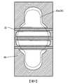
圖1係表示實施方式之半導體裝置(半導體封裝)之剖視圖。圖1所示之半導體封裝1具備:配線基板2、搭載於配線基板2上之第1半導體晶片3、填埋第1半導體晶片3且接著於配線基板2之第1接著層(FOD)4、與第1接著層4接著且固定於不具備電極之第2半導體晶片5上之複數個第3半導體晶片6之積層體7、及以將第1半導體晶片3或第3半導體晶片6之積層體7等密封之方式設置於配線基板2上之密封樹脂層8。第2半導體晶片5為間隔基板且使用矽晶圓,但另外亦可將聚醯亞胺等樹脂或玻璃等之板用作間隔基板。FIG. 1 is a cross-sectional view showing a semiconductor device (semiconductor package) according to the embodiment. The semiconductor package 1 shown in FIG. 1 includes: a
配線基板2例如具有由設置於絕緣性樹脂基板或絕緣性陶瓷基板等之表面之配線層9或設置於內部之配線層10等構成之配線網。作為絕緣性材料,具體而言有玻璃-環氧樹脂複合材、玻璃、聚醯亞胺樹脂、矽氧化物、矽氮化物等絕緣材料。配線層9、10例如由銅或銅合金、金或金合金等、銀或銀合金、鋁、鎢、鈦、鎳等金屬材料構成。配線基板2具有成為外部端子之形成面等之第1面2a、及成為半導體晶片3、5、6之搭載面之第2面2b。The
於配線基板2之第2面2b上,搭載有第1半導體晶片3,第1半導體晶片3填埋於第1接著層(FOD)4內且接著於配線基板2之晶片搭載區域。作為第1半導體晶片3,例如可列舉於用作第3半導體晶片6之半導體記憶體晶片與外部設備之間收發數位信號之控制器晶片或接口晶片、邏輯晶片、RF(radio frequency,射頻)晶片等系統LSI(Large Scale Integration,大規模積體電路)晶片,但並不限定於此。On the second surface 2 b of the
第1半導體晶片3之電極(未圖示)經由接合線11而與配線基板2之配線層9電連接。藉由將控制器晶片等第1半導體晶片3直接搭載於配線基板2上,可縮短第1半導體晶片3與配線基板2之間之配線長。藉此,謀求提高第1半導體晶片3與配線基板2之間之信號傳輸速度等,能夠應對半導體封裝1之高速化。進而,由於第1半導體晶片3填埋於第1接著層4內,故而不會降低第3半導體晶片6相對於配線基板2之搭載性,另外亦不會妨礙封裝尺寸之小型化等。因此,能夠提供小型且應對高速元件之半導體封裝1。The electrodes (not shown) of the
一般而言,控制器晶片等第1半導體晶片3之外形形狀與半導體記憶體晶片等第3半導體晶片6之外形形狀相比較小。因此,將搭載於配線基板2上之第1半導體晶片3填埋於第1接著層4內,然後於第1接著層4上積層並搭載複數個第3半導體晶片6。作為第3半導體晶片6之具體例,可列舉NAND(Not And,與非)型快閃記憶體般之半導體記憶體晶片,但並不限定於此。於本實施方式中,將4個半導體記憶體晶片作為第3半導體晶片6積層並搭載。再者,第3半導體晶片6之積層數並不限定為4段。In general, the outer shape of the first semiconductor wafer 3 such as a controller chip is smaller than the outer shape of the third semiconductor wafer 6 such as a semiconductor memory wafer. Therefore, the first semiconductor wafer 3 mounted on the
搭載於第1接著層4上之複數個第3半導體晶片6中,第1段至第4段為止之第3半導體晶片6以各自之電極露出之方式,於第1方向(圖中為紙面右方向)上使排列電極之端部錯開地積層成階梯狀。Among the plurality of third semiconductor wafers 6 mounted on the first
複數個第3半導體晶片6中第1段之第3半導體晶片6固定於不具備電極之第2半導體晶片5上。第2半導體晶片5經由第1接著層4而固定於第1半導體晶片3之上。第1接著層4使用普通之DAF(Die Attach Film,晶粒黏接膜)等接著劑。第3半導體晶片6利用於圖1中省略了圖示之DAF等接著劑,固定於位於下側之第2半導體晶片5或第3半導體晶片6。第3半導體晶片6之電極(未圖示)經由接合線12而與配線基板2之配線層9電連接。關於電氣特性或信號特性相等之電極焊墊,能夠將配線基板2之配線層9與複數個第3半導體晶片6之電極焊墊利用接合線12依次連接。即,第1段至第4段之第3半導體晶片6之電極利用接合線12依次連接,第1段之第3半導體晶片6之電極與配線基板2之配線層9利用接合線12連接。半導體晶片之厚度例如為30μm~100μm。The third semiconductor wafer 6 of the first stage among the plurality of third semiconductor wafers 6 is fixed to the
於配線基板2之第2面2b上,以將第1半導體晶片3或第3半導體晶片6之積層體7與接合線11、12一起密封之方式,將使用環氧樹脂等絕緣樹脂之密封樹脂層8例如模塑成形。藉由該等構成要素,構成實施方式之半導體封裝1。On the second surface 2b of the
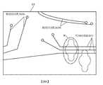
接下來,參照圖2~圖6對半導體封裝1之配線基板2之構成進行說明。如圖2、3所示,配線基板2具有第1配線層21、第2配線層23、及第3配線層24。第1配線層21、第2配線層23、及第3配線層24分別大致平行。Next, the structure of the
圖5係第1配線層21中之配線圖案之平面模式圖。於第1配線層21,設置有高速配線焊盤20a、連接於高速配線焊盤20a之第1層高速配線20、信號配線焊盤22a、連接於信號配線焊盤22a之第1層信號配線22b、電源用焊盤X及接地用焊盤Y。各配線經由通孔28而將第1配線層21、第2配線層23、及第3配線層24之間連接。於I部分,自高速配線焊盤20a經由通孔將高速配線連接於第2配線層23。於II部分,第1層高速配線20自高速配線焊盤20a延伸,經由通孔28將高速配線連接於第2配線層23。於高速配線焊盤20a、信號配線焊盤22a、電源用焊盤X及接地用焊盤Y,形成焊接凸塊等而與未圖示之外部設備連接。FIG. 5 is a schematic plan view of the wiring pattern in the
圖6係第2配線層23中之配線圖案之平面模式圖。於第2配線層23,設置有第2層高速配線20c及第2層信號配線22。分別經由通孔自第1配線層21連接。另外,如觀察由單點鏈線III包圍之部位可知,存在高速配線焊盤20a與第2層信號配線22重疊之部位。FIG. 6 is a schematic plan view of the wiring pattern in the
如圖2、3所示,於第3配線層24,設置有電源配線25及接地配線26。電源配線25位於第1配線層21側,於其上配置有接地配線26。經由電源用焊盤X與接地用焊盤Y對電源配線25與接地配線26供電。設置於第3配線層24之電源配線25與接地配線26中之至少一者用作屏蔽產生於高速配線焊盤20a與第2層信號配線22之間之雜訊之雜訊屏蔽配線。再者,於第1配線層21、第2配線層23中,未設置配線或焊墊之部分配置有整面狀或網狀之電源配線或接地配線,但於圖5、6中省略了上述部件。於本實施方式中,對將接地配線26用作雜訊屏蔽配線之情況進行說明。As shown in FIGS. 2 and 3, the
以下,對高速配線進行說明。Hereinafter, the high-speed wiring will be described.
高速配線例如為PCIe(Peripheral Component Interconnect Express)等高速配線,係流通頻率例如為1GHz以上之信號之配線,且需要阻抗控制。於信號配線中流通頻率較高速配線慢之信號。高速配線焊盤20a具有較第1層高速配線20之線寬大之直徑,成為佔據較大面積之導體部。又,第1層高速配線20及第2層高速配線20c係以2根為一組之對配線,其配線圖案相互類似。高速配線較佳為成對使用。例如,高速配線20僅連接於必須以高速交換信號之第1半導體晶片3。例如,信號配線22存在自信號配線焊盤22a出來後連接於第1半導體晶片3之情況、自信號配線焊盤22a出來後連接於第3半導體晶片6之情況、及將第1半導體晶片3與第3半導體晶片6連接之情況。The high-speed wiring is, for example, PCIe (Peripheral Component Interconnect Express) and other high-speed wiring, which is a wiring that circulates signals with a frequency of, for example, 1 GHz or more, and requires impedance control. Signals with a slower frequency than high-speed wiring circulate in the signal wiring. The high-
如上所述,高速配線焊盤20a成為佔據較大面積之導體部。因此,若高速配線焊盤20a之部分與接地配線26重疊,則其等之間之電容耦合變大。因此,如圖2所示,於本實施方式中,於上層之第2配線層23之第2層信號配線22與高速配線焊盤20a不重疊之部分,不配置(去除)於其等之間用作雜訊屏蔽配線之接地配線26。As described above, the high-
又,如圖3所示,於上層之第2配線層23之第2層信號配線22與高速配線焊盤20a重疊之部分,以與第2層信號配線22重疊之方式配置有於其等之間用作雜訊屏蔽配線之接地配線26。Furthermore, as shown in FIG. 3, the portion where the second
圖4係將圖6之由單點鏈線III包圍之部分放大並透視地表示之模式圖。表示了設置有第2配線層23之第2層信號配線22與接地配線26之部分。高速配線焊盤20a之外形由虛線表示。如上所述,於第1配線層21之高速配線焊盤20a與第2配線層23之第2層信號配線22之間,將用作雜訊屏蔽配線之接地配線26以介置於第1配線層21之高速配線焊盤20a與第2配線層23之第2層信號配線22之間之方式配設。而且,如圖4所示,於與高速配線焊盤20a重疊之部分,對應於高速配線焊盤20a之形狀而形成有未設置接地配線26之區域。另一方面,以橫穿高速配線焊盤20a之上之方式,於形成有第2層信號配線22之部分,換句話說於高速配線焊盤20a與第2層信號配線22重疊之部分,與第2層信號配線22重疊地設置有接地配線26。Fig. 4 is a schematic diagram of the part enclosed by the single-dot chain line III of Fig. 6 enlarged and shown in perspective. The portion where the second
接地配線26以與通過高速配線焊盤20a之第2層信號配線22之配線圖案相同之配線圖案形成。為了容易理解,於圖4中,第2層信號配線22之線寬描繪得較接地配線26之線寬為細,但基本上,較佳為與第2層信號配線22之線寬大致相同。然而,接地配線26之線寬未必與第2層信號配線22之線寬大致相同,例如,於將第2層信號配線22之線寬設為10時,亦可將接地配線26之線寬設為增加5~15之線寬。即接地配線26之線寬可設為第2層信號配線22之1.5倍至2.5倍。再者,第2層信號配線22等之線寬例如為30μm至35μm左右。The
藉由擴大接地配線26之線寬,高速配線焊盤20a與第2層信號配線22之間之雜訊降低效果變高,但高速配線焊盤20a與接地配線26之電容耦合變多。另一方面,藉由縮窄接地配線26之線寬,能夠降低高速配線焊盤20a與接地配線26之電容耦合,但高速配線焊盤20a與第2層信號配線22之間之雜訊降低效果變低。By enlarging the line width of the
因此,如上所述,當將第2層信號配線22之線寬設為10時,接地配線26之線寬設為5~15之間之線寬。即接地配線26之線寬可設為第2層信號配線22之0.5倍至1.5倍。藉此,能夠減輕高速配線焊盤20a與第2層信號配線22之間之雜訊影響,且抑制高速配線焊盤20a與接地配線26之電容耦合而抑制電氣特性之惡化。Therefore, as described above, when the line width of the second
配線基板2由絕緣層與形成於該絕緣層之導體層構成。絕緣層能夠由至少包含樹脂、陶瓷、玻璃、聚醯亞胺、矽之任一種之絕緣材料形成。又,導體層能夠由銅、鋁、鎢、金、銀之任一種或包含該等金屬之合金形成。The
如上所述,於本實施方式之配線基板2及半導體封裝1中,能夠減輕配線層間之雜訊影響,且抑制電容耦合。As described above, in the
實際上,製成使用實施例之配線基板2之半導體封裝1,實施例之配線基板2係於與高速配線焊盤20a重疊之部分,對應於高速配線焊盤20a之形狀而形成未設置接地配線26之區域,於高速配線焊盤20a與第2層信號配線22重疊之部分,以與第2層信號配線22重疊之方式設置有與第2層信號配線22相同線寬之接地配線26。另一方面,製成使用比較例之配線基板2之半導體封裝1,比較例之配線基板2係於與高速配線焊盤20a重疊之部分仍一樣地(立體地)設置有接地配線26。然後,對其等之電性能進行比較。In fact, a semiconductor package 1 using the
於上述電性能之比較中,關於回損(Return Loss),關於差模(Differential mode)及共模(Common mode)之參考時脈(REFCLK),於頻率50MHz-2.5GHz、2.5GHz-8GHz下進行測定並比較。In the above electrical performance comparison, regarding the return loss (Return Loss), regarding the differential mode (Differential mode) and the common mode (Common mode) reference clock (REFCLK), under the frequency 50MHz-2.5GHz, 2.5GHz-8GHz Make measurements and compare.
結果,於差模之參考時脈中,與比較例相比,實施例獲得良好之結果,例如,50MHz-2.5GHz下為-0.58dB,2.5GHz-8GHz下為-0.48dB。又,於共模之參考時脈中,與比較例相比,實施例獲得良好之結果,例如,50MHz-2.5GHz下為-0.39dB,2.5GHz-8GHz下為-0.28dB。As a result, in the reference clock of the differential mode, compared with the comparative example, the embodiment obtains good results, for example, -0.58dB under 50MHz-2.5GHz, and -0.48dB under 2.5GHz-8GHz. Moreover, in the reference clock of the common mode, compared with the comparative example, the embodiment obtains good results, for example, -0.39dB under 50MHz-2.5GHz, and -0.28dB under 2.5GHz-8GHz.
其他實施方式。Other embodiments.
(a)於上述實施方式中,將接地配線26用作屏蔽,但亦可將電源配線25用作屏蔽。或者,亦可將電源配線25與接地配線26之兩者用於屏蔽。(a) In the above embodiment, the
(b)於上述實施方式中,接地配線26處於電源配線25之上,但亦可為電源配線25處於上側,接地配線26處於下側。(b) In the above embodiment, the
(c)於上述實施方式中,接地配線26或電源配線25屏蔽之係高速配線焊盤20a,但亦可屏蔽信號配線焊盤22a。(c) In the above embodiment, the high-
(d)於上述實施方式中,如圖2、圖3所示,接地配線26處於電源配線25之上,疑似成為兩層,但亦可將電源配線25與接地配線26設置於同一層。(d) In the above embodiment, as shown in FIGS. 2 and 3, the
以上,已對本發明之幾個實施方式進行了說明,但該等實施方式係作為示例而提出者,並非意圖限定發明之範圍。該等新穎之實施方式能夠以其他各種方式實施,能於不脫離發明之主旨之範圍內進行各種省略、置換、變更。該等實施方式或其變化包含於發明之範圍或主旨中,並且包含於申請專利範圍中所記載之發明及其均等之範圍中。Although several embodiments of the present invention have been described above, these embodiments are presented as examples and are not intended to limit the scope of the invention. These novel embodiments can be implemented in various other ways, and various omissions, substitutions, and changes can be made without departing from the spirit of the invention. These embodiments or their changes are included in the scope or spirit of the invention, and are included in the invention described in the scope of the patent application and its equivalent scope.
本申請案基於2020年03月17日提出申請之在先日本專利申請案第2020-046216號之優先權而主張優先權利益,藉由引用將其全部內容併入本文中。This application claims priority rights based on the priority of the prior Japanese Patent Application No. 2020-046216 filed on March 17, 2020, and the entire content is incorporated herein by reference.
20:第1層高速配線20: Layer 1 high-speed wiring
20a:高速配線焊盤20a: High-speed wiring pad
21:第1配線層21: The first wiring layer
22:第2層信號配線22:
23:第2配線層23: 2nd wiring layer
24:第3配線層24: 3rd wiring layer
25:電源配線25: Power wiring
26:接地配線26: Ground wiring
Claims (9)
Translated fromChineseApplications Claiming Priority (2)
| Application Number | Priority Date | Filing Date | Title |
|---|---|---|---|
| JP2020-046216 | 2020-03-17 | ||
| JP2020046216AJP7326192B2 (en) | 2020-03-17 | 2020-03-17 | Wiring board and semiconductor device |
Publications (2)
| Publication Number | Publication Date |
|---|---|
| TWI740569Btrue TWI740569B (en) | 2021-09-21 |
| TW202137842A TW202137842A (en) | 2021-10-01 |
Family
ID=77677328
Family Applications (1)
| Application Number | Title | Priority Date | Filing Date |
|---|---|---|---|
| TW109123224ATWI740569B (en) | 2020-03-17 | 2020-07-09 | Wiring board and semiconductor device |
Country Status (4)
| Country | Link |
|---|---|
| US (1) | US11688678B2 (en) |
| JP (1) | JP7326192B2 (en) |
| CN (1) | CN113410204B (en) |
| TW (1) | TWI740569B (en) |
Families Citing this family (1)
| Publication number | Priority date | Publication date | Assignee | Title |
|---|---|---|---|---|
| US11605581B2 (en)* | 2021-01-08 | 2023-03-14 | Renesas Electronics Corporation | Semiconductor device having conductive patterns with mesh pattern and differential signal wirings |
Citations (4)
| Publication number | Priority date | Publication date | Assignee | Title |
|---|---|---|---|---|
| TW493365B (en)* | 2000-01-21 | 2002-07-01 | Toshiba Corp | Wiring board, semiconductor package, and semiconductor device |
| WO2013035888A1 (en)* | 2011-09-09 | 2013-03-14 | 日本電気株式会社 | Wiring board |
| TW201713172A (en)* | 2015-09-25 | 2017-04-01 | Dainippon Printing Co Ltd | Mounting component, wiring board, electronic device, and methods for manufacturing same |
| TW201819324A (en)* | 2016-09-13 | 2018-06-01 | 日商旭硝子股份有限公司 | Glass substrate for high frequency device and circuit substrate for high frequency device |
Family Cites Families (20)
| Publication number | Priority date | Publication date | Assignee | Title |
|---|---|---|---|---|
| JP2000156549A (en)* | 1998-11-20 | 2000-06-06 | Sega Enterp Ltd | Printed wiring board and game device equipped with the same |
| JP3542517B2 (en)* | 1999-04-27 | 2004-07-14 | Necエレクトロニクス株式会社 | Semiconductor device |
| US6510545B1 (en)* | 2000-01-19 | 2003-01-21 | Sun Microsystems, Inc. | Automated shielding algorithm for dynamic circuits |
| JP2001250825A (en) | 2000-03-06 | 2001-09-14 | Nec Microsystems Ltd | Multilayered wiring structure |
| US7002253B2 (en) | 2003-04-30 | 2006-02-21 | Matsushita Electric Industrial Co., Ltd. | Semiconductor device and design method thereof |
| US7227247B2 (en)* | 2005-02-16 | 2007-06-05 | Intel Corporation | IC package with signal land pads |
| JP4919475B2 (en) | 2006-07-13 | 2012-04-18 | ルネサスエレクトロニクス株式会社 | Manufacturing method of semiconductor integrated circuit |
| US7894199B1 (en)* | 2008-02-20 | 2011-02-22 | Altera Corporation | Hybrid package |
| KR101817156B1 (en)* | 2010-12-28 | 2018-01-10 | 삼성전자 주식회사 | Semiconductor device of stacked structure having through electrode, semiconductor memory device, semiconductor memory system and operating method thereof |
| JP2014022652A (en)* | 2012-07-20 | 2014-02-03 | Elpida Memory Inc | Semiconductor device and test equipment therefor, and semiconductor device test method |
| JP6122606B2 (en)* | 2012-10-16 | 2017-04-26 | ルネサスエレクトロニクス株式会社 | Semiconductor device |
| US20140252632A1 (en)* | 2013-03-06 | 2014-09-11 | Hans-Joachim Barth | Semiconductor devices |
| US9099533B2 (en)* | 2013-07-02 | 2015-08-04 | International Business Machines Corporation | Semiconductor device with distinct multiple-patterned conductive tracks on a same level |
| WO2015162768A1 (en)* | 2014-04-24 | 2015-10-29 | ルネサスエレクトロニクス株式会社 | Semiconductor device and method for producing same |
| US10276519B2 (en)* | 2015-06-02 | 2019-04-30 | Sarcina Technology LLC | Package substrate differential impedance optimization for 25 to 60 Gbps and beyond |
| JP2017146767A (en)* | 2016-02-17 | 2017-08-24 | 株式会社ジャパンディスプレイ | Display device |
| US10354976B2 (en)* | 2016-07-22 | 2019-07-16 | Invensas Corporation | Dies-on-package devices and methods therefor |
| JP2019129181A (en)* | 2018-01-22 | 2019-08-01 | ルネサスエレクトロニクス株式会社 | Semiconductor device |
| JP7001530B2 (en)* | 2018-04-16 | 2022-01-19 | ルネサスエレクトロニクス株式会社 | Semiconductor device |
| JP6535788B2 (en)* | 2018-06-06 | 2019-06-26 | ルネサスエレクトロニクス株式会社 | Semiconductor device |
- 2020
- 2020-03-17JPJP2020046216Apatent/JP7326192B2/enactiveActive
- 2020-07-09TWTW109123224Apatent/TWI740569B/enactive
- 2020-08-03CNCN202010768154.0Apatent/CN113410204B/enactiveActive
- 2020-08-28USUS17/005,575patent/US11688678B2/enactiveActive
Patent Citations (4)
| Publication number | Priority date | Publication date | Assignee | Title |
|---|---|---|---|---|
| TW493365B (en)* | 2000-01-21 | 2002-07-01 | Toshiba Corp | Wiring board, semiconductor package, and semiconductor device |
| WO2013035888A1 (en)* | 2011-09-09 | 2013-03-14 | 日本電気株式会社 | Wiring board |
| TW201713172A (en)* | 2015-09-25 | 2017-04-01 | Dainippon Printing Co Ltd | Mounting component, wiring board, electronic device, and methods for manufacturing same |
| TW201819324A (en)* | 2016-09-13 | 2018-06-01 | 日商旭硝子股份有限公司 | Glass substrate for high frequency device and circuit substrate for high frequency device |
Also Published As
| Publication number | Publication date |
|---|---|
| US20210296223A1 (en) | 2021-09-23 |
| US11688678B2 (en) | 2023-06-27 |
| TW202137842A (en) | 2021-10-01 |
| CN113410204A (en) | 2021-09-17 |
| CN113410204B (en) | 2024-04-09 |
| JP2021150363A (en) | 2021-09-27 |
| JP7326192B2 (en) | 2023-08-15 |
Similar Documents
| Publication | Publication Date | Title |
|---|---|---|
| US12027465B2 (en) | Impedance controlled electrical interconnection employing meta-materials | |
| JP4185499B2 (en) | Semiconductor device | |
| JP6449760B2 (en) | Semiconductor device | |
| US6489676B2 (en) | Semiconductor device having an interconnecting post formed on an interposer within a sealing resin | |
| JP6352447B2 (en) | Semiconductor device | |
| US6924549B2 (en) | Semiconductor device and a method of manufacturing the same | |
| US6608376B1 (en) | Integrated circuit package substrate with high density routing mechanism | |
| US7453153B2 (en) | Circuit device | |
| US8129759B2 (en) | Semiconductor package and method using isolated VSS plane to accommodate high speed circuitry ground isolation | |
| US20160172289A1 (en) | Circuit substrate and package structure | |
| US8310062B2 (en) | Stacked semiconductor package | |
| CN111696970A (en) | Semiconductor device with a plurality of semiconductor chips | |
| TWI740569B (en) | Wiring board and semiconductor device | |
| US9905517B2 (en) | Semiconductor device | |
| EP1944802B1 (en) | Semiconductor package product | |
| US20070029663A1 (en) | Multilayered circuit substrate and semiconductor package structure using the same | |
| JP6535788B2 (en) | Semiconductor device | |
| CN113410212B (en) | Semiconductor device with a semiconductor device having a plurality of semiconductor chips | |
| JP2006332708A (en) | Semiconductor device | |
| JP2011216522A (en) | Semiconductor device | |
| CN116072638A (en) | semiconductor package |