TWI740552B - Semiconductor device - Google Patents
Semiconductor deviceDownload PDFInfo
- Publication number
- TWI740552B TWI740552BTW109121363ATW109121363ATWI740552BTW I740552 BTWI740552 BTW I740552BTW 109121363 ATW109121363 ATW 109121363ATW 109121363 ATW109121363 ATW 109121363ATW I740552 BTWI740552 BTW I740552B
- Authority
- TW
- Taiwan
- Prior art keywords
- layer
- insulating layer
- oxide
- film
- oxide semiconductor
- Prior art date
Links
- 239000004065semiconductorSubstances0.000titleclaimsabstractdescription401
- 239000000758substrateSubstances0.000claimsdescription80
- 229910052581Si3N4Inorganic materials0.000claimsdescription76
- HQVNEWCFYHHQES-UHFFFAOYSA-Nsilicon nitrideChemical compoundN12[Si]34N5[Si]62N3[Si]51N64HQVNEWCFYHHQES-UHFFFAOYSA-N0.000claimsdescription76
- 238000000034methodMethods0.000claimsdescription64
- 239000013078crystalSubstances0.000claimsdescription40
- 229910052738indiumInorganic materials0.000claimsdescription30
- 229910052733galliumInorganic materials0.000claimsdescription28
- 238000004435EPR spectroscopyMethods0.000claimsdescription13
- 229910052725zincInorganic materials0.000claimsdescription10
- 239000002159nanocrystalSubstances0.000claimsdescription3
- IJGRMHOSHXDMSA-UHFFFAOYSA-NAtomic nitrogenChemical compoundN#NIJGRMHOSHXDMSA-UHFFFAOYSA-N0.000abstractdescription115
- 229910052757nitrogenInorganic materials0.000abstractdescription54
- XUIMIQQOPSSXEZ-UHFFFAOYSA-NSiliconChemical compound[Si]XUIMIQQOPSSXEZ-UHFFFAOYSA-N0.000abstractdescription44
- 229910052710siliconInorganic materials0.000abstractdescription44
- 239000010703siliconSubstances0.000abstractdescription44
- 229910052751metalInorganic materials0.000abstractdescription39
- 239000000470constituentSubstances0.000abstractdescription25
- 230000006378damageEffects0.000abstractdescription9
- 230000003247decreasing effectEffects0.000abstract1
- 239000010410layerSubstances0.000description861
- 239000010408filmSubstances0.000description300
- 239000007789gasSubstances0.000description68
- 239000000463materialSubstances0.000description53
- 239000011701zincSubstances0.000description53
- QGZKDVFQNNGYKY-UHFFFAOYSA-NAmmoniaChemical compoundNQGZKDVFQNNGYKY-UHFFFAOYSA-N0.000description50
- 229910052760oxygenInorganic materials0.000description50
- 239000001301oxygenSubstances0.000description50
- QVGXLLKOCUKJST-UHFFFAOYSA-Natomic oxygenChemical compound[O]QVGXLLKOCUKJST-UHFFFAOYSA-N0.000description46
- 239000001257hydrogenSubstances0.000description42
- 229910052739hydrogenInorganic materials0.000description42
- 239000004973liquid crystal related substanceSubstances0.000description41
- UFHFLCQGNIYNRP-UHFFFAOYSA-NHydrogenChemical compound[H][H]UFHFLCQGNIYNRP-UHFFFAOYSA-N0.000description35
- 238000010438heat treatmentMethods0.000description32
- 230000001681protective effectEffects0.000description32
- 238000004519manufacturing processMethods0.000description29
- 239000012535impuritySubstances0.000description28
- 229910021529ammoniaInorganic materials0.000description25
- BLRPTPMANUNPDV-UHFFFAOYSA-NSilaneChemical compound[SiH4]BLRPTPMANUNPDV-UHFFFAOYSA-N0.000description23
- 239000000203mixtureSubstances0.000description22
- 229910000077silaneInorganic materials0.000description22
- 230000015572biosynthetic processEffects0.000description21
- 238000009413insulationMethods0.000description20
- 239000002184metalSubstances0.000description20
- 230000007547defectEffects0.000description19
- 230000006870functionEffects0.000description18
- 239000012071phaseSubstances0.000description18
- 238000005268plasma chemical vapour depositionMethods0.000description18
- XLOMVQKBTHCTTD-UHFFFAOYSA-NZinc monoxideChemical compound[Zn]=OXLOMVQKBTHCTTD-UHFFFAOYSA-N0.000description16
- 238000005401electroluminescenceMethods0.000description15
- 238000011282treatmentMethods0.000description15
- 239000011229interlayerSubstances0.000description14
- VYPSYNLAJGMNEJ-UHFFFAOYSA-NSilicium dioxideChemical compoundO=[Si]=OVYPSYNLAJGMNEJ-UHFFFAOYSA-N0.000description13
- 229910021417amorphous siliconInorganic materials0.000description13
- 238000010586diagramMethods0.000description13
- APFVFJFRJDLVQX-UHFFFAOYSA-Nindium atomChemical compound[In]APFVFJFRJDLVQX-UHFFFAOYSA-N0.000description13
- GQPLMRYTRLFLPF-UHFFFAOYSA-NNitrous OxideChemical compound[O-][N+]#NGQPLMRYTRLFLPF-UHFFFAOYSA-N0.000description12
- 239000002245particleSubstances0.000description12
- 238000012360testing methodMethods0.000description12
- -1etc.Substances0.000description11
- 230000008569processEffects0.000description11
- 229920005989resinPolymers0.000description11
- 239000011347resinSubstances0.000description11
- 238000004544sputter depositionMethods0.000description11
- GYHNNYVSQQEPJS-UHFFFAOYSA-NGalliumChemical compound[Ga]GYHNNYVSQQEPJS-UHFFFAOYSA-N0.000description10
- 229910052782aluminiumInorganic materials0.000description9
- 230000015556catabolic processEffects0.000description9
- 239000010949copperSubstances0.000description9
- XKRFYHLGVUSROY-UHFFFAOYSA-NArgonChemical compound[Ar]XKRFYHLGVUSROY-UHFFFAOYSA-N0.000description8
- XAGFODPZIPBFFR-UHFFFAOYSA-NaluminiumChemical compound[Al]XAGFODPZIPBFFR-UHFFFAOYSA-N0.000description8
- 229910052802copperInorganic materials0.000description8
- 229910044991metal oxideInorganic materials0.000description8
- 150000004706metal oxidesChemical class0.000description8
- 229910052814silicon oxideInorganic materials0.000description8
- 239000010936titaniumSubstances0.000description8
- 229910052721tungstenInorganic materials0.000description8
- XLYOFNOQVPJJNP-UHFFFAOYSA-NwaterSubstancesOXLYOFNOQVPJJNP-UHFFFAOYSA-N0.000description8
- 239000011787zinc oxideSubstances0.000description8
- RYGMFSIKBFXOCR-UHFFFAOYSA-NCopperChemical compound[Cu]RYGMFSIKBFXOCR-UHFFFAOYSA-N0.000description7
- 208000005156DehydrationDiseases0.000description7
- 210000004027cellAnatomy0.000description7
- 230000018044dehydrationEffects0.000description7
- 238000006297dehydration reactionMethods0.000description7
- 238000006356dehydrogenation reactionMethods0.000description7
- 238000005530etchingMethods0.000description7
- 238000011156evaluationMethods0.000description7
- 150000002431hydrogenChemical class0.000description7
- 229910003437indium oxideInorganic materials0.000description7
- PJXISJQVUVHSOJ-UHFFFAOYSA-Nindium(iii) oxideChemical compound[O-2].[O-2].[O-2].[In+3].[In+3]PJXISJQVUVHSOJ-UHFFFAOYSA-N0.000description7
- AMGQUBHHOARCQH-UHFFFAOYSA-Nindium;oxotinChemical compound[In].[Sn]=OAMGQUBHHOARCQH-UHFFFAOYSA-N0.000description7
- 238000005468ion implantationMethods0.000description7
- 239000003566sealing materialSubstances0.000description7
- 239000010409thin filmSubstances0.000description7
- 229910052719titaniumInorganic materials0.000description7
- CURLTUGMZLYLDI-UHFFFAOYSA-NCarbon dioxideChemical compoundO=C=OCURLTUGMZLYLDI-UHFFFAOYSA-N0.000description6
- MYMOFIZGZYHOMD-UHFFFAOYSA-NDioxygenChemical compoundO=OMYMOFIZGZYHOMD-UHFFFAOYSA-N0.000description6
- 239000012298atmosphereSubstances0.000description6
- 239000003990capacitorSubstances0.000description6
- 239000000969carrierSubstances0.000description6
- 150000001875compoundsChemical class0.000description6
- 229910001882dioxygenInorganic materials0.000description6
- 230000005684electric fieldEffects0.000description6
- 239000005262ferroelectric liquid crystals (FLCs)Substances0.000description6
- 239000011521glassSubstances0.000description6
- 239000001272nitrous oxideSubstances0.000description6
- 239000010937tungstenSubstances0.000description6
- HEZMWWAKWCSUCB-PHDIDXHHSA-N(3R,4R)-3,4-dihydroxycyclohexa-1,5-diene-1-carboxylic acidChemical compoundO[C@@H]1C=CC(C(O)=O)=C[C@H]1OHEZMWWAKWCSUCB-PHDIDXHHSA-N0.000description5
- 238000003917TEM imageMethods0.000description5
- 230000004888barrier functionEffects0.000description5
- 238000005229chemical vapour depositionMethods0.000description5
- 230000005611electricityEffects0.000description5
- 150000002483hydrogen compoundsChemical class0.000description5
- 239000011810insulating materialSubstances0.000description5
- 238000002156mixingMethods0.000description5
- 150000004767nitridesChemical class0.000description5
- 239000010453quartzSubstances0.000description5
- 239000004925Acrylic resinSubstances0.000description4
- 229920000178Acrylic resinPolymers0.000description4
- GWEVSGVZZGPLCZ-UHFFFAOYSA-NTitan oxideChemical compoundO=[Ti]=OGWEVSGVZZGPLCZ-UHFFFAOYSA-N0.000description4
- RTAQQCXQSZGOHL-UHFFFAOYSA-NTitaniumChemical compound[Ti]RTAQQCXQSZGOHL-UHFFFAOYSA-N0.000description4
- 229910007541Zn OInorganic materials0.000description4
- 229910052786argonInorganic materials0.000description4
- 125000004429atomChemical group0.000description4
- 239000005380borophosphosilicate glassSubstances0.000description4
- 239000011651chromiumSubstances0.000description4
- 239000003086colorantSubstances0.000description4
- 229920001940conductive polymerPolymers0.000description4
- 238000001514detection methodMethods0.000description4
- AJNVQOSZGJRYEI-UHFFFAOYSA-Ndigallium;oxygen(2-)Chemical compound[O-2].[O-2].[O-2].[Ga+3].[Ga+3]AJNVQOSZGJRYEI-UHFFFAOYSA-N0.000description4
- 230000000694effectsEffects0.000description4
- 238000005516engineering processMethods0.000description4
- 230000001747exhibiting effectEffects0.000description4
- 230000005669field effectEffects0.000description4
- 238000011049fillingMethods0.000description4
- 229910001195gallium oxideInorganic materials0.000description4
- 239000003094microcapsuleSubstances0.000description4
- 229910052750molybdenumInorganic materials0.000description4
- QJGQUHMNIGDVPM-UHFFFAOYSA-Nnitrogen groupChemical group[N]QJGQUHMNIGDVPM-UHFFFAOYSA-N0.000description4
- QGLKJKCYBOYXKC-UHFFFAOYSA-NnonaoxidotritungstenChemical compoundO=[W]1(=O)O[W](=O)(=O)O[W](=O)(=O)O1QGLKJKCYBOYXKC-UHFFFAOYSA-N0.000description4
- 230000003287optical effectEffects0.000description4
- 150000002894organic compoundsChemical class0.000description4
- 238000005192partitionMethods0.000description4
- 239000005360phosphosilicate glassSubstances0.000description4
- 229920001721polyimidePolymers0.000description4
- 239000002356single layerSubstances0.000description4
- 125000006850spacer groupChemical group0.000description4
- 239000003381stabilizerSubstances0.000description4
- OGIDPMRJRNCKJF-UHFFFAOYSA-Ntitanium oxideInorganic materials[Ti]=OOGIDPMRJRNCKJF-UHFFFAOYSA-N0.000description4
- 229910001930tungsten oxideInorganic materials0.000description4
- PXHVJJICTQNCMI-UHFFFAOYSA-NNickelChemical compound[Ni]PXHVJJICTQNCMI-UHFFFAOYSA-N0.000description3
- 229910003902SiCl 4Inorganic materials0.000description3
- 229910020994Sn-ZnInorganic materials0.000description3
- 229910009069Sn—ZnInorganic materials0.000description3
- NRTOMJZYCJJWKI-UHFFFAOYSA-NTitanium nitrideChemical compound[Ti]#NNRTOMJZYCJJWKI-UHFFFAOYSA-N0.000description3
- 238000000231atomic layer depositionMethods0.000description3
- 230000008901benefitEffects0.000description3
- 230000005540biological transmissionEffects0.000description3
- 229910002092carbon dioxideInorganic materials0.000description3
- 239000001569carbon dioxideSubstances0.000description3
- SLLGVCUQYRMELA-UHFFFAOYSA-NchlorosiliconChemical compoundCl[Si]SLLGVCUQYRMELA-UHFFFAOYSA-N0.000description3
- 230000003098cholesteric effectEffects0.000description3
- 229910052804chromiumInorganic materials0.000description3
- 238000002425crystallisationMethods0.000description3
- 230000008025crystallizationEffects0.000description3
- 230000006866deteriorationEffects0.000description3
- 238000009792diffusion processMethods0.000description3
- 239000003822epoxy resinSubstances0.000description3
- 150000002500ionsChemical class0.000description3
- 238000004518low pressure chemical vapour depositionMethods0.000description3
- 230000007246mechanismEffects0.000description3
- 239000007769metal materialSubstances0.000description3
- BASFCYQUMIYNBI-UHFFFAOYSA-NplatinumChemical compound[Pt]BASFCYQUMIYNBI-UHFFFAOYSA-N0.000description3
- 229910021420polycrystalline siliconInorganic materials0.000description3
- 229920000647polyepoxidePolymers0.000description3
- 239000009719polyimide resinSubstances0.000description3
- 229920002620polyvinyl fluoridePolymers0.000description3
- 238000005036potential barrierMethods0.000description3
- 238000012545processingMethods0.000description3
- 229920002050silicone resinPolymers0.000description3
- 238000003860storageMethods0.000description3
- 229910052715tantalumInorganic materials0.000description3
- WFKWXMTUELFFGS-UHFFFAOYSA-NtungstenChemical compound[W]WFKWXMTUELFFGS-UHFFFAOYSA-N0.000description3
- 238000001947vapour-phase growthMethods0.000description3
- YVTHLONGBIQYBO-UHFFFAOYSA-Nzinc indium(3+) oxygen(2-)Chemical compound[O--].[Zn++].[In+3]YVTHLONGBIQYBO-UHFFFAOYSA-N0.000description3
- PAYRUJLWNCNPSJ-UHFFFAOYSA-NAnilineChemical compoundNC1=CC=CC=C1PAYRUJLWNCNPSJ-UHFFFAOYSA-N0.000description2
- OKTJSMMVPCPJKN-UHFFFAOYSA-NCarbonChemical compound[C]OKTJSMMVPCPJKN-UHFFFAOYSA-N0.000description2
- VYZAMTAEIAYCRO-UHFFFAOYSA-NChromiumChemical compound[Cr]VYZAMTAEIAYCRO-UHFFFAOYSA-N0.000description2
- 206010052128GlareDiseases0.000description2
- ZOKXTWBITQBERF-UHFFFAOYSA-NMolybdenumChemical compound[Mo]ZOKXTWBITQBERF-UHFFFAOYSA-N0.000description2
- 229910052779NeodymiumInorganic materials0.000description2
- OAICVXFJPJFONN-UHFFFAOYSA-NPhosphorusChemical compound[P]OAICVXFJPJFONN-UHFFFAOYSA-N0.000description2
- KAESVJOAVNADME-UHFFFAOYSA-NPyrroleChemical compoundC=1C=CNC=1KAESVJOAVNADME-UHFFFAOYSA-N0.000description2
- 229910052772SamariumInorganic materials0.000description2
- 229910020923Sn-OInorganic materials0.000description2
- 229910006404SnO 2Inorganic materials0.000description2
- YTPLMLYBLZKORZ-UHFFFAOYSA-NThiopheneChemical compoundC=1C=CSC=1YTPLMLYBLZKORZ-UHFFFAOYSA-N0.000description2
- ATJFFYVFTNAWJD-UHFFFAOYSA-NTinChemical compound[Sn]ATJFFYVFTNAWJD-UHFFFAOYSA-N0.000description2
- 238000002441X-ray diffractionMethods0.000description2
- 239000012790adhesive layerSubstances0.000description2
- 239000000956alloySubstances0.000description2
- GPBUGPUPKAGMDK-UHFFFAOYSA-NazanylidynemolybdenumChemical compound[Mo]#NGPBUGPUPKAGMDK-UHFFFAOYSA-N0.000description2
- UMIVXZPTRXBADB-UHFFFAOYSA-NbenzocyclobuteneChemical compoundC1=CC=C2CCC2=C1UMIVXZPTRXBADB-UHFFFAOYSA-N0.000description2
- 239000005388borosilicate glassSubstances0.000description2
- 238000000180cavity ring-down spectroscopyMethods0.000description2
- 230000008859changeEffects0.000description2
- 238000006243chemical reactionMethods0.000description2
- 238000004891communicationMethods0.000description2
- 239000004020conductorSubstances0.000description2
- 238000006731degradation reactionMethods0.000description2
- 238000003795desorptionMethods0.000description2
- 238000011161developmentMethods0.000description2
- 230000018109developmental processEffects0.000description2
- 238000007598dipping methodMethods0.000description2
- 239000006185dispersionSubstances0.000description2
- 239000005038ethylene vinyl acetateSubstances0.000description2
- 230000005281excited stateEffects0.000description2
- 239000011152fibreglassSubstances0.000description2
- 229910052735hafniumInorganic materials0.000description2
- VBJZVLUMGGDVMO-UHFFFAOYSA-Nhafnium atomChemical compound[Hf]VBJZVLUMGGDVMO-UHFFFAOYSA-N0.000description2
- 229910052734heliumInorganic materials0.000description2
- 239000001307heliumSubstances0.000description2
- SWQJXJOGLNCZEY-UHFFFAOYSA-Nhelium atomChemical compound[He]SWQJXJOGLNCZEY-UHFFFAOYSA-N0.000description2
- 125000002887hydroxy groupChemical group[H]O*0.000description2
- 238000012905input functionMethods0.000description2
- 150000002739metalsChemical class0.000description2
- 238000001451molecular beam epitaxyMethods0.000description2
- 239000011733molybdenumSubstances0.000description2
- QEFYFXOXNSNQGX-UHFFFAOYSA-Nneodymium atomChemical compound[Nd]QEFYFXOXNSNQGX-UHFFFAOYSA-N0.000description2
- 229910052754neonInorganic materials0.000description2
- GKAOGPIIYCISHV-UHFFFAOYSA-Nneon atomChemical compound[Ne]GKAOGPIIYCISHV-UHFFFAOYSA-N0.000description2
- 239000010955niobiumSubstances0.000description2
- 238000007645offset printingMethods0.000description2
- 239000011368organic materialSubstances0.000description2
- TWNQGVIAIRXVLR-UHFFFAOYSA-Noxo(oxoalumanyloxy)alumaneChemical compoundO=[Al]O[Al]=OTWNQGVIAIRXVLR-UHFFFAOYSA-N0.000description2
- 125000004430oxygen atomChemical groupO*0.000description2
- 230000000737periodic effectEffects0.000description2
- 229910052698phosphorusInorganic materials0.000description2
- 239000011574phosphorusSubstances0.000description2
- 239000000049pigmentSubstances0.000description2
- 229920003023plasticPolymers0.000description2
- 229920001200poly(ethylene-vinyl acetate)Polymers0.000description2
- 229920002037poly(vinyl butyral) polymerPolymers0.000description2
- 229920006122polyamide resinPolymers0.000description2
- 229920006267polyester filmPolymers0.000description2
- 229920005591polysiliconPolymers0.000description2
- 229920000915polyvinyl chloridePolymers0.000description2
- 239000004800polyvinyl chlorideSubstances0.000description2
- 238000010248power generationMethods0.000description2
- 238000007639printingMethods0.000description2
- 230000006798recombinationEffects0.000description2
- 238000005215recombinationMethods0.000description2
- KZUNJOHGWZRPMI-UHFFFAOYSA-Nsamarium atomChemical compound[Sm]KZUNJOHGWZRPMI-UHFFFAOYSA-N0.000description2
- 238000007650screen-printingMethods0.000description2
- VSZWPYCFIRKVQL-UHFFFAOYSA-Nselanylidenegallium;seleniumChemical compound[Se].[Se]=[Ga].[Se]=[Ga]VSZWPYCFIRKVQL-UHFFFAOYSA-N0.000description2
- 238000009751slip formingMethods0.000description2
- 239000002904solventSubstances0.000description2
- 238000004611spectroscopical analysisMethods0.000description2
- 238000004528spin coatingMethods0.000description2
- 238000005507sprayingMethods0.000description2
- 230000003068static effectEffects0.000description2
- GUVRBAGPIYLISA-UHFFFAOYSA-Ntantalum atomChemical compound[Ta]GUVRBAGPIYLISA-UHFFFAOYSA-N0.000description2
- UWCWUCKPEYNDNV-LBPRGKRZSA-N2,6-dimethyl-n-[[(2s)-pyrrolidin-2-yl]methyl]anilineChemical compoundCC1=CC=CC(C)=C1NC[C@H]1NCCC1UWCWUCKPEYNDNV-LBPRGKRZSA-N0.000description1
- MGWGWNFMUOTEHG-UHFFFAOYSA-N4-(3,5-dimethylphenyl)-1,3-thiazol-2-amineChemical compoundCC1=CC(C)=CC(C=2N=C(N)SC=2)=C1MGWGWNFMUOTEHG-UHFFFAOYSA-N0.000description1
- 229910018120Al-Ga-ZnInorganic materials0.000description1
- 229910018137Al-ZnInorganic materials0.000description1
- 229910018573Al—ZnInorganic materials0.000description1
- ZOXJGFHDIHLPTG-UHFFFAOYSA-NBoronChemical compound[B]ZOXJGFHDIHLPTG-UHFFFAOYSA-N0.000description1
- UGFAIRIUMAVXCW-UHFFFAOYSA-NCarbon monoxideChemical compound[O+]#[C-]UGFAIRIUMAVXCW-UHFFFAOYSA-N0.000description1
- 229910052684CeriumInorganic materials0.000description1
- 229910052692DysprosiumInorganic materials0.000description1
- 229910052691ErbiumInorganic materials0.000description1
- 229910052693EuropiumInorganic materials0.000description1
- 229910005191Ga 2 O 3Inorganic materials0.000description1
- 108010083687Ion PumpsProteins0.000description1
- HBBGRARXTFLTSG-UHFFFAOYSA-NLithium ionChemical compound[Li+]HBBGRARXTFLTSG-UHFFFAOYSA-N0.000description1
- 239000004642PolyimideSubstances0.000description1
- 229910000577Silicon-germaniumInorganic materials0.000description1
- BQCADISMDOOEFD-UHFFFAOYSA-NSilverChemical compound[Ag]BQCADISMDOOEFD-UHFFFAOYSA-N0.000description1
- 239000004990Smectic liquid crystalSubstances0.000description1
- 229910020833Sn-Al-ZnInorganic materials0.000description1
- 229910020868Sn-Ga-ZnInorganic materials0.000description1
- 239000004974Thermotropic liquid crystalSubstances0.000description1
- 229910052769YtterbiumInorganic materials0.000description1
- LEVVHYCKPQWKOP-UHFFFAOYSA-N[Si].[Ge]Chemical compound[Si].[Ge]LEVVHYCKPQWKOP-UHFFFAOYSA-N0.000description1
- 230000001133accelerationEffects0.000description1
- NIXOWILDQLNWCW-UHFFFAOYSA-Nacrylic acid groupChemical groupC(C=C)(=O)ONIXOWILDQLNWCW-UHFFFAOYSA-N0.000description1
- 230000009471actionEffects0.000description1
- 239000000853adhesiveSubstances0.000description1
- 230000001070adhesive effectEffects0.000description1
- 239000002313adhesive filmSubstances0.000description1
- 229910045601alloyInorganic materials0.000description1
- NWAIGJYBQQYSPW-UHFFFAOYSA-NazanylidyneindiganeChemical compound[In]#NNWAIGJYBQQYSPW-UHFFFAOYSA-N0.000description1
- 229910052788bariumInorganic materials0.000description1
- DSAJWYNOEDNPEQ-UHFFFAOYSA-Nbarium atomChemical compound[Ba]DSAJWYNOEDNPEQ-UHFFFAOYSA-N0.000description1
- 230000000903blocking effectEffects0.000description1
- 229910052796boronInorganic materials0.000description1
- 238000004364calculation methodMethods0.000description1
- 229910052799carbonInorganic materials0.000description1
- 125000004432carbon atomChemical groupC*0.000description1
- 229910002091carbon monoxideInorganic materials0.000description1
- 239000000919ceramicSubstances0.000description1
- GWXLDORMOJMVQZ-UHFFFAOYSA-NceriumChemical compound[Ce]GWXLDORMOJMVQZ-UHFFFAOYSA-N0.000description1
- 229910017052cobaltInorganic materials0.000description1
- 239000010941cobaltSubstances0.000description1
- GUTLYIVDDKVIGB-UHFFFAOYSA-Ncobalt atomChemical compound[Co]GUTLYIVDDKVIGB-UHFFFAOYSA-N0.000description1
- 238000004040coloringMethods0.000description1
- 238000001816coolingMethods0.000description1
- 150000004696coordination complexChemical class0.000description1
- 229920001577copolymerPolymers0.000description1
- 210000002858crystal cellAnatomy0.000description1
- 230000001419dependent effectEffects0.000description1
- 238000000151depositionMethods0.000description1
- 238000013461designMethods0.000description1
- KBQHZAAAGSGFKK-UHFFFAOYSA-Ndysprosium atomChemical compound[Dy]KBQHZAAAGSGFKK-UHFFFAOYSA-N0.000description1
- 238000005538encapsulationMethods0.000description1
- UYAHIZSMUZPPFV-UHFFFAOYSA-NerbiumChemical compound[Er]UYAHIZSMUZPPFV-UHFFFAOYSA-N0.000description1
- OGPBJKLSAFTDLK-UHFFFAOYSA-Neuropium atomChemical compound[Eu]OGPBJKLSAFTDLK-UHFFFAOYSA-N0.000description1
- 230000004438eyesightEffects0.000description1
- 239000000945fillerSubstances0.000description1
- 238000007667floatingMethods0.000description1
- 239000011888foilSubstances0.000description1
- 230000004313glareEffects0.000description1
- 229910021389grapheneInorganic materials0.000description1
- 239000004519greaseSubstances0.000description1
- 239000005431greenhouse gasSubstances0.000description1
- 230000005283ground stateEffects0.000description1
- 230000012010growthEffects0.000description1
- 230000012447hatchingEffects0.000description1
- 229910001385heavy metalInorganic materials0.000description1
- 150000004678hydridesChemical class0.000description1
- 125000004435hydrogen atomChemical group[H]*0.000description1
- 238000007654immersionMethods0.000description1
- 230000006872improvementEffects0.000description1
- 239000011261inert gasSubstances0.000description1
- 150000002484inorganic compoundsChemical class0.000description1
- 229910010272inorganic materialInorganic materials0.000description1
- 229910052742ironInorganic materials0.000description1
- 229910052746lanthanumInorganic materials0.000description1
- FZLIPJUXYLNCLC-UHFFFAOYSA-Nlanthanum atomChemical compound[La]FZLIPJUXYLNCLC-UHFFFAOYSA-N0.000description1
- 238000001307laser spectroscopyMethods0.000description1
- 239000003446ligandSubstances0.000description1
- 229910001416lithium ionInorganic materials0.000description1
- 230000033001locomotionEffects0.000description1
- 230000007774longtermEffects0.000description1
- 238000004020luminiscence typeMethods0.000description1
- 230000014759maintenance of locationEffects0.000description1
- 229910052748manganeseInorganic materials0.000description1
- 238000007567mass-production techniqueMethods0.000description1
- 239000011159matrix materialSubstances0.000description1
- 238000002844meltingMethods0.000description1
- 230000008018meltingEffects0.000description1
- 239000012528membraneSubstances0.000description1
- 239000013081microcrystalSubstances0.000description1
- 229910021424microcrystalline siliconInorganic materials0.000description1
- 239000000178monomerSubstances0.000description1
- 229910052759nickelInorganic materials0.000description1
- RUFLMLWJRZAWLJ-UHFFFAOYSA-Nnickel silicideChemical compound[Ni]=[Si]=[Ni]RUFLMLWJRZAWLJ-UHFFFAOYSA-N0.000description1
- 229910021334nickel silicideInorganic materials0.000description1
- 229910052758niobiumInorganic materials0.000description1
- GUCVJGMIXFAOAE-UHFFFAOYSA-Nniobium atomChemical compound[Nb]GUCVJGMIXFAOAE-UHFFFAOYSA-N0.000description1
- 239000012299nitrogen atmosphereSubstances0.000description1
- 125000004433nitrogen atomChemical groupN*0.000description1
- JCXJVPUVTGWSNB-UHFFFAOYSA-Nnitrogen dioxideInorganic materialsO=[N]=OJCXJVPUVTGWSNB-UHFFFAOYSA-N0.000description1
- 238000010943off-gassingMethods0.000description1
- 239000012788optical filmSubstances0.000description1
- 230000003071parasitic effectEffects0.000description1
- 238000001782photodegradationMethods0.000description1
- 229920002120photoresistant polymerPolymers0.000description1
- 230000000704physical effectEffects0.000description1
- 238000002294plasma sputter depositionMethods0.000description1
- 238000009832plasma treatmentMethods0.000description1
- 239000004033plasticSubstances0.000description1
- 229910052697platinumInorganic materials0.000description1
- 230000010287polarizationEffects0.000description1
- 229920000767polyanilinePolymers0.000description1
- 229920000642polymerPolymers0.000description1
- 239000003505polymerization initiatorSubstances0.000description1
- 229920000128polypyrrolePolymers0.000description1
- 229920000123polythiophenePolymers0.000description1
- 230000000750progressive effectEffects0.000description1
- 150000003254radicalsChemical class0.000description1
- 230000009467reductionEffects0.000description1
- 230000003252repetitive effectEffects0.000description1
- 230000004044responseEffects0.000description1
- 230000000717retained effectEffects0.000description1
- 239000010980sapphireSubstances0.000description1
- 229910052594sapphireInorganic materials0.000description1
- 229910052706scandiumInorganic materials0.000description1
- SIXSYDAISGFNSX-UHFFFAOYSA-Nscandium atomChemical compound[Sc]SIXSYDAISGFNSX-UHFFFAOYSA-N0.000description1
- 238000007789sealingMethods0.000description1
- 229910021332silicideInorganic materials0.000description1
- FVBUAEGBCNSCDD-UHFFFAOYSA-Nsilicide(4-)Chemical compound[Si-4]FVBUAEGBCNSCDD-UHFFFAOYSA-N0.000description1
- 229910052990silicon hydrideInorganic materials0.000description1
- 229910052709silverInorganic materials0.000description1
- 239000004332silverSubstances0.000description1
- 238000005477sputtering targetMethods0.000description1
- 230000006641stabilisationEffects0.000description1
- 238000011105stabilizationMethods0.000description1
- 229910001220stainless steelInorganic materials0.000description1
- 239000010935stainless steelSubstances0.000description1
- 238000000859sublimationMethods0.000description1
- 230000008022sublimationEffects0.000description1
- MZLGASXMSKOWSE-UHFFFAOYSA-Ntantalum nitrideChemical compound[Ta]#NMZLGASXMSKOWSE-UHFFFAOYSA-N0.000description1
- JBQYATWDVHIOAR-UHFFFAOYSA-NtellanylidenegermaniumChemical compound[Te]=[Ge]JBQYATWDVHIOAR-UHFFFAOYSA-N0.000description1
- 229920001187thermosetting polymerPolymers0.000description1
- 229930192474thiopheneNatural products0.000description1
- XOLBLPGZBRYERU-UHFFFAOYSA-Ntin dioxideChemical compoundO=[Sn]=OXOLBLPGZBRYERU-UHFFFAOYSA-N0.000description1
- 229910001887tin oxideInorganic materials0.000description1
- 150000003608titaniumChemical class0.000description1
- 238000002834transmittanceMethods0.000description1
- LEONUFNNVUYDNQ-UHFFFAOYSA-Nvanadium atomChemical compound[V]LEONUFNNVUYDNQ-UHFFFAOYSA-N0.000description1
- 238000007740vapor depositionMethods0.000description1
- NAWDYIZEMPQZHO-UHFFFAOYSA-NytterbiumChemical compound[Yb]NAWDYIZEMPQZHO-UHFFFAOYSA-N0.000description1
- AKJVMGQSGCSQBU-UHFFFAOYSA-Nzinc azanidylidenezincChemical compound[Zn++].[N-]=[Zn].[N-]=[Zn]AKJVMGQSGCSQBU-UHFFFAOYSA-N0.000description1
- OYQCBJZGELKKPM-UHFFFAOYSA-Nzinc indium(3+) oxygen(2-)Chemical compound[O-2].[Zn+2].[O-2].[In+3]OYQCBJZGELKKPM-UHFFFAOYSA-N0.000description1
Images


Classifications
- H—ELECTRICITY
- H10—SEMICONDUCTOR DEVICES; ELECTRIC SOLID-STATE DEVICES NOT OTHERWISE PROVIDED FOR
- H10D—INORGANIC ELECTRIC SEMICONDUCTOR DEVICES
- H10D30/00—Field-effect transistors [FET]
- H10D30/60—Insulated-gate field-effect transistors [IGFET]
- H10D30/67—Thin-film transistors [TFT]
- H10D30/674—Thin-film transistors [TFT] characterised by the active materials
- H10D30/6755—Oxide semiconductors, e.g. zinc oxide, copper aluminium oxide or cadmium stannate
- H—ELECTRICITY
- H10—SEMICONDUCTOR DEVICES; ELECTRIC SOLID-STATE DEVICES NOT OTHERWISE PROVIDED FOR
- H10D—INORGANIC ELECTRIC SEMICONDUCTOR DEVICES
- H10D30/00—Field-effect transistors [FET]
- H10D30/60—Insulated-gate field-effect transistors [IGFET]
- H10D30/67—Thin-film transistors [TFT]
- H10D30/6729—Thin-film transistors [TFT] characterised by the electrodes
- H10D30/673—Thin-film transistors [TFT] characterised by the electrodes characterised by the shapes, relative sizes or dispositions of the gate electrodes
- H—ELECTRICITY
- H10—SEMICONDUCTOR DEVICES; ELECTRIC SOLID-STATE DEVICES NOT OTHERWISE PROVIDED FOR
- H10D—INORGANIC ELECTRIC SEMICONDUCTOR DEVICES
- H10D30/00—Field-effect transistors [FET]
- H10D30/60—Insulated-gate field-effect transistors [IGFET]
- H10D30/67—Thin-film transistors [TFT]
- H10D30/6757—Thin-film transistors [TFT] characterised by the structure of the channel, e.g. transverse or longitudinal shape or doping profile
- H—ELECTRICITY
- H10—SEMICONDUCTOR DEVICES; ELECTRIC SOLID-STATE DEVICES NOT OTHERWISE PROVIDED FOR
- H10D—INORGANIC ELECTRIC SEMICONDUCTOR DEVICES
- H10D62/00—Semiconductor bodies, or regions thereof, of devices having potential barriers
- H10D62/40—Crystalline structures
- H10D62/405—Orientations of crystalline planes
- H—ELECTRICITY
- H10—SEMICONDUCTOR DEVICES; ELECTRIC SOLID-STATE DEVICES NOT OTHERWISE PROVIDED FOR
- H10D—INORGANIC ELECTRIC SEMICONDUCTOR DEVICES
- H10D64/00—Electrodes of devices having potential barriers
- H10D64/60—Electrodes characterised by their materials
- H10D64/66—Electrodes having a conductor capacitively coupled to a semiconductor by an insulator, e.g. MIS electrodes
- H10D64/68—Electrodes having a conductor capacitively coupled to a semiconductor by an insulator, e.g. MIS electrodes characterised by the insulator, e.g. by the gate insulator
- H10D64/681—Electrodes having a conductor capacitively coupled to a semiconductor by an insulator, e.g. MIS electrodes characterised by the insulator, e.g. by the gate insulator having a compositional variation, e.g. multilayered
- H10D64/685—Electrodes having a conductor capacitively coupled to a semiconductor by an insulator, e.g. MIS electrodes characterised by the insulator, e.g. by the gate insulator having a compositional variation, e.g. multilayered being perpendicular to the channel plane
- H—ELECTRICITY
- H10—SEMICONDUCTOR DEVICES; ELECTRIC SOLID-STATE DEVICES NOT OTHERWISE PROVIDED FOR
- H10D—INORGANIC ELECTRIC SEMICONDUCTOR DEVICES
- H10D64/00—Electrodes of devices having potential barriers
- H10D64/60—Electrodes characterised by their materials
- H10D64/66—Electrodes having a conductor capacitively coupled to a semiconductor by an insulator, e.g. MIS electrodes
- H10D64/68—Electrodes having a conductor capacitively coupled to a semiconductor by an insulator, e.g. MIS electrodes characterised by the insulator, e.g. by the gate insulator
- H10D64/691—Electrodes having a conductor capacitively coupled to a semiconductor by an insulator, e.g. MIS electrodes characterised by the insulator, e.g. by the gate insulator comprising metallic compounds, e.g. metal oxides or metal silicates
- H—ELECTRICITY
- H10—SEMICONDUCTOR DEVICES; ELECTRIC SOLID-STATE DEVICES NOT OTHERWISE PROVIDED FOR
- H10D—INORGANIC ELECTRIC SEMICONDUCTOR DEVICES
- H10D64/00—Electrodes of devices having potential barriers
- H10D64/60—Electrodes characterised by their materials
- H10D64/66—Electrodes having a conductor capacitively coupled to a semiconductor by an insulator, e.g. MIS electrodes
- H10D64/68—Electrodes having a conductor capacitively coupled to a semiconductor by an insulator, e.g. MIS electrodes characterised by the insulator, e.g. by the gate insulator
- H10D64/693—Electrodes having a conductor capacitively coupled to a semiconductor by an insulator, e.g. MIS electrodes characterised by the insulator, e.g. by the gate insulator the insulator comprising nitrogen, e.g. nitrides, oxynitrides or nitrogen-doped materials
Landscapes
- Thin Film Transistor (AREA)
- Solid State Image Pick-Up Elements (AREA)
- Electroluminescent Light Sources (AREA)
- Liquid Crystal (AREA)
- Mechanical Treatment Of Semiconductor (AREA)
- Bipolar Transistors (AREA)
- Noodles (AREA)
Abstract
Description
Translated fromChinese本說明書所公開的發明係關於一種半導體裝置及半導體裝置的製造方法。The invention disclosed in this specification relates to a semiconductor device and a method of manufacturing the semiconductor device.
注意,本說明書等中的半導體裝置是指藉由利用半導體特性而能夠工作的所有裝置,因此電光裝置、發光顯示裝置、半導體電路以及電子裝置都是半導體裝置。Note that semiconductor devices in this specification and the like refer to all devices that can operate by utilizing semiconductor characteristics, and therefore electro-optical devices, light-emitting display devices, semiconductor circuits, and electronic devices are all semiconductor devices.
使用形成在具有絕緣表面的基板上的半導體薄膜構成電晶體的技術受到關注。該電晶體被廣泛地應用於如積體電路(IC)及影像顯示裝置(有時簡稱為顯示裝置)等的電子裝置。作為可以應用於電晶體的半導體薄膜,矽類半導體材料被廣泛地周知。作為其他材料,氧化物半導體受到關注。A technique of using a semiconductor thin film formed on a substrate with an insulating surface to construct a transistor is attracting attention. The transistor is widely used in electronic devices such as integrated circuits (ICs) and image display devices (sometimes simply referred to as display devices). As semiconductor thin films that can be applied to transistors, silicon-based semiconductor materials are widely known. As other materials, oxide semiconductors are attracting attention.
例如,公開了作為氧化物半導體使用氧化鋅或In-Ga-Zn類氧化物半導體來製造電晶體的技術(參照專利文獻1及專利文獻2)。For example, a technique of manufacturing a transistor using zinc oxide or an In-Ga-Zn-based oxide semiconductor as an oxide semiconductor is disclosed (see
[專利文獻1]日本專利申請公開第2007-123861號公報[Patent Document 1] Japanese Patent Application Publication No. 2007-123861Report
[專利文獻2]日本專利申請公開第2007-96055號公報[Patent Document 2] Japanese Patent Application Publication No. 2007-96055
在進行使用氧化物半導體的半導體裝置的大量生產(以下,簡稱為量產)的情況下,從開發成本及開發速度的角度來看,有效的是利用實用化了的量產技術,即利用使用非晶矽或多晶矽等矽類半導體材料的電晶體的結構、製程條件或生產裝置等。In the case of mass production of semiconductor devices using oxide semiconductors (hereinafter referred to as mass production), from the perspective of development cost and development speed, it is effective to use practical mass production technology, that is, to use The structure, process conditions, or production equipment of transistors made of silicon-based semiconductor materials such as amorphous silicon or polycrystalline silicon.
另一方面,氧化物半導體的載流子產生機制與矽類半導體材料的載流子產生機制大不相同,該氧化物半導體的物性極大地影響到電晶體特性或電晶體的可靠性。On the other hand, the carrier generation mechanism of an oxide semiconductor is quite different from that of silicon-based semiconductor materials, and the physical properties of the oxide semiconductor greatly affect the characteristics of the transistor or the reliability of the transistor.
尤其是,當將用於矽類半導體材料的閘極絕緣層用於氧化物半導體時,閘極絕緣層與該氧化物半導體之間的介面特性不夠好。因此,需要開發適於使用氧化物半導體的半導體裝置的閘極絕緣層。In particular, when a gate insulating layer used for a silicon-based semiconductor material is used for an oxide semiconductor, the interface characteristics between the gate insulating layer and the oxide semiconductor are not good enough. Therefore, it is necessary to develop a gate insulating layer suitable for a semiconductor device using an oxide semiconductor.
另外,由使用非晶矽或微晶矽等矽類半導體材料的電晶體構成的半導體裝置可應用於第八代(2160mm長×2460mm寬)或更高代的玻璃基板,所以具有生產性高及成本低的優點。然而,當使用玻璃基板時,由於玻璃基板具有較高的絕緣性及較大的面積,靜電放電(ESD:Electro-Static Discharge)的問題尤其明顯。這是在使用氧化物半導體材料的情況下當然也需要考慮的問題。In addition, semiconductor devices composed of transistors using silicon-based semiconductor materials such as amorphous silicon or microcrystalline silicon can be applied to glass substrates of the eighth generation (2160mm long x 2460mm wide) or higher, so it has high productivity and The advantage of low cost. However, when a glass substrate is used, the problem of electrostatic discharge (ESD: Electro-Static Discharge) is particularly obvious because the glass substrate has higher insulation and a larger area. This is of course a problem that needs to be considered when using oxide semiconductor materials.
鑒於上述問題,本發明的一個方式的目的之一是在不太改變實用化了的量產技術的電晶體結構、製程條件或生產裝置等的情況下提供一種具有穩定的電特性和高可靠性的半導體裝置。In view of the above problems, one of the objectives of one aspect of the present invention is to provide a stable electrical characteristic and high reliability without changing the transistor structure, process conditions, or production equipment of the practical mass production technology. Of semiconductor devices.
另外,本發明的一個方式是提供一種能夠防止由靜電破壞引起的良率的下降的半導體裝置。In addition, one aspect of the present invention is to provide a semiconductor device capable of preventing a decrease in yield due to electrostatic destruction.
本發明的一個方式是一種半導體裝置,該半導體裝置在閘極電極層與氧化物半導體層之間包括從閘極電極層一側依次層疊含有氮的矽膜與含有從氧化物半導體層的構成元素中選擇的一種或多種金屬元素的氧化物絕緣層的疊層結構。One aspect of the present invention is a semiconductor device that includes a silicon film containing nitrogen and a constituent element containing the oxide semiconductor layer layered in order from the gate electrode layer side between the gate electrode layer and the oxide semiconductor layer. The laminated structure of the oxide insulating layer of one or more metal elements selected in the.
與氧化矽膜相比,含有氮的矽膜的介電常數高,因此為了得到相等的靜電容量所需要的厚度大。由此,藉由使用含有氮的矽膜構成閘極絕緣層,可以在物理上加厚閘極絕緣層而可以抑制絕緣耐壓的下降,可以較佳為提高絕緣耐壓。因此,可以抑制這樣的包括閘極絕緣層的半導體裝置的靜電破壞。Compared with a silicon oxide film, a silicon film containing nitrogen has a higher dielectric constant, so the thickness required to obtain the same capacitance is large. Therefore, by using a silicon film containing nitrogen to form the gate insulating layer, the gate insulating layer can be physically thickened and the decrease in the withstand voltage can be suppressed, and the withstand voltage can preferably be improved. Therefore, it is possible to suppress the electrostatic breakdown of such a semiconductor device including the gate insulating layer.
較佳的是,將含有氮的矽膜的厚度設定為325nm以上且550nm以下,更較佳為355nm以上且550nm以下。此外,作為含有氮的矽膜,使用氮化矽膜較佳。Preferably, the thickness of the silicon film containing nitrogen is set to be 325 nm or more and 550 nm or less, more preferably 355 nm or more and 550 nm or less. In addition, as the silicon film containing nitrogen, a silicon nitride film is preferably used.
因為含有氮的矽膜也作為非晶矽或多晶矽等矽類半導體材料的閘極絕緣層被實用化,所以可以轉用製程條件或生產裝置等。因此,藉由將含有氮的矽膜適用於閘極絕緣層,可以以低成本量產使用氧化物半導體的電晶體。Since silicon films containing nitrogen are also used as gate insulating layers for silicon-based semiconductor materials such as amorphous silicon or polysilicon, they can be converted to process conditions or production equipment. Therefore, by applying a silicon film containing nitrogen to the gate insulating layer, a transistor using an oxide semiconductor can be mass-produced at low cost.
另外,藉由以接觸於氧化物半導體層的方式設置使用從氧化物半導體層的構成元素中選擇的一種或多種金屬元素的氧化物絕緣層,可以良好地保持該氧化物絕緣層和氧化物半導體層之間的介面狀態,而能夠防止介面的退化。尤其藉由抑制在氧化物絕緣層和氧化物半導體層之間的介面上的載流子的捕獲,可以減少電晶體的光劣化(例如光負偏壓劣化),而能夠得到可靠性高的電晶體。In addition, by providing an oxide insulating layer using one or more metal elements selected from the constituent elements of the oxide semiconductor layer in contact with the oxide semiconductor layer, the oxide insulating layer and the oxide semiconductor can be maintained well. The state of the interface between the layers can prevent the degradation of the interface. In particular, by suppressing the trapping of carriers on the interface between the oxide insulating layer and the oxide semiconductor layer, it is possible to reduce the photodegradation of the transistor (for example, the photonegative bias degradation), and it is possible to obtain highly reliable electricity. Crystal.
就是說,根據本發明的一個方式,藉由利用一部分已被實用化的矽類半導體材料的量產技術並採用包括含有氮的矽膜、含有從氧化物半導體層的構成元素中選擇的一種或多種金屬元素的氧化物絕緣層以及氧化物半導體層的疊層結構,來可以提供與使用矽類半導體材料的半導體裝置不同並發揮新效果的半導體裝置。明確而言,可以採用下面的結構。That is, according to one aspect of the present invention, by using a mass production technology of a part of silicon-based semiconductor materials that has been put into practical use, and adopting a silicon film containing nitrogen, containing one or one selected from the constituent elements of the oxide semiconductor layer The laminated structure of the oxide insulating layer and the oxide semiconductor layer of various metal elements can provide a semiconductor device that is different from a semiconductor device using a silicon-based semiconductor material and exerts a new effect. Specifically, the following structure can be adopted.
本發明的一個方式是一種半導體裝置,包括:閘極電極層;閘極電極層上的閘極絕緣層;閘極絕緣層上的氧化物絕緣層;接觸於氧化物絕緣層上並重疊於閘極電極層的氧化物半導體層;以及電連接到氧化物半導體層的源極電極層及汲極電極,其中閘極絕緣層包括含有氮的矽膜,氧化物絕緣層含有從氧化物半導體層的構成元素中選擇的一種或多種金屬元素,閘極絕緣層的厚度比氧化物絕緣層的厚度厚。One aspect of the present invention is a semiconductor device including: a gate electrode layer; a gate insulating layer on the gate electrode layer; an oxide insulating layer on the gate insulating layer; contacting the oxide insulating layer and overlapping the gate The oxide semiconductor layer of the electrode electrode layer; and the source electrode layer and the drain electrode electrically connected to the oxide semiconductor layer, wherein the gate insulating layer includes a silicon film containing nitrogen, and the oxide insulating layer contains For one or more metal elements selected from the constituent elements, the thickness of the gate insulating layer is thicker than the thickness of the oxide insulating layer.
在上述半導體裝置中,較佳為氧化物半導體層和氧化物絕緣層的端部一致。另外,在本說明書等中,一致也包括大概一致。例如,使用同一個遮罩進行蝕刻的疊層結構的層A的端部和層B的端部被看作一致。In the above-mentioned semiconductor device, it is preferable that the end portions of the oxide semiconductor layer and the oxide insulating layer coincide. In addition, in this manual, etc., consistency is also includedIncluding roughly the same. For example, the end of the layer A and the end of the layer B of the laminated structure that are etched using the same mask are regarded as the same.
除了接觸於氧化物半導體層的下層而設置的含有從氧化物半導體層的構成元素中選擇的一種或多種金屬元素的氧化物絕緣層和含有氮的矽膜的疊層結構,也可以接觸於氧化物半導體層的上層地設置該疊層結構。藉由採用該結構,可以對半導體裝置賦予穩定的電特性及/或能夠進一步地防止半導體裝置的靜電破壞。In addition to the laminated structure of an oxide insulating layer containing one or more metal elements selected from the constituent elements of the oxide semiconductor layer and a silicon film containing nitrogen, which is provided in contact with the lower layer of the oxide semiconductor layer, it may also be in contact with the oxide semiconductor layer. The laminated structure is arranged on the upper layer of the semiconductor layer. By adopting this structure, stable electrical characteristics can be imparted to the semiconductor device and/or electrostatic destruction of the semiconductor device can be further prevented.
就是說,本發明的另一個方式是一種半導體裝置,包括:閘極電極層;閘極電極層上的閘極絕緣層;閘極絕緣層上的第一氧化物絕緣層;接觸於第一氧化物絕緣層上並重疊於閘極電極層的氧化物半導體層;電連接到氧化物半導體層的源極電極層及汲極電極層;覆蓋源極電極層及汲極電極層並接觸於氧化物半導體層的一部分的第二氧化物絕緣層;以及第二氧化物絕緣層上的保護絕緣層,其中閘極絕緣層及保護絕緣層包括含有氮的矽膜,第一氧化物絕緣層及第二氧化物絕緣層含有從氧化物半導體層的構成元素中選擇的一種或多種的金屬元素,閘極絕緣層的厚度比第一氧化物絕緣層的厚度厚,保護絕緣層的厚度比第二氧化物絕緣層的厚度厚。That is, another aspect of the present invention is a semiconductor device including: a gate electrode layer; a gate insulating layer on the gate electrode layer; a first oxide insulating layer on the gate insulating layer; The oxide semiconductor layer on the insulating layer and overlapping the gate electrode layer; the source electrode layer and the drain electrode layer electrically connected to the oxide semiconductor layer; cover the source electrode layer and the drain electrode layer and contact the oxide A second oxide insulating layer that is part of the semiconductor layer; and a protective insulating layer on the second oxide insulating layer, wherein the gate insulating layer and the protective insulating layer include a silicon film containing nitrogen, the first oxide insulating layer and the second insulating layer The oxide insulating layer contains one or more metal elements selected from the constituent elements of the oxide semiconductor layer, the thickness of the gate insulating layer is thicker than that of the first oxide insulating layer, and the thickness of the protective insulating layer is greater than that of the second oxide. The thickness of the insulating layer is thick.
另外,在上述半導體裝置中,較佳為氧化物半導體層與第一氧化物絕緣層的端部一致。In addition, in the above-mentioned semiconductor device, it is preferable that the oxide semiconductor layer coincides with the end of the first oxide insulating layer.
另外,在上述半導體裝置的任一種中,閘極絕緣層的厚度較佳為325nm以上且550nm以下。另外,作為閘極絕緣層,使用氮化矽膜較佳。In addition, in any of the aforementioned semiconductor devices, the thickness of the gate insulating layer is preferably 325 nm or more and 550 nm or less. In addition, as a gateFor the insulating layer, a silicon nitride film is preferably used.
此外,接觸於氧化物半導體層的氧化物絕緣層較佳為包括超過化學計量組成的氧的區域(以下,也稱為氧過剩區域)。藉由使接觸於氧化物半導體層的氧化物絕緣層包括氧過剩區域,可以對氧化物半導體層提供氧。對氧化物半導體來說,氧缺陷成為施體,而在氧化物半導體中生成成為載流子的電子,因此藉由對氧化物半導體層供應氧而填補氧缺陷,來能夠提供可靠性高的電晶體。In addition, the oxide insulating layer in contact with the oxide semiconductor layer is preferably a region containing oxygen exceeding the stoichiometric composition (hereinafter, also referred to as an oxygen excess region). By making the oxide insulating layer in contact with the oxide semiconductor layer include the oxygen excess region, oxygen can be supplied to the oxide semiconductor layer. For oxide semiconductors, oxygen defects become donors, and electrons that become carriers are generated in the oxide semiconductor. Therefore, by supplying oxygen to the oxide semiconductor layer to fill the oxygen defects, it is possible to provide highly reliable electricity. Crystal.
藉由本發明的一個方式提供的半導體裝置是利用與實用化了的量產技術相差不多的製造方法製造的具有穩定的電特性和高可靠性的半導體裝置。The semiconductor device provided by one aspect of the present invention is a semiconductor device with stable electrical characteristics and high reliability manufactured by a manufacturing method similar to a practical mass production technology.
另外,藉由本發明的一個方式可以提供能夠防止由靜電破壞引起的良率的下降的半導體裝置。In addition, according to one aspect of the present invention, it is possible to provide a semiconductor device capable of preventing a decrease in yield due to electrostatic breakdown.
300:電晶體300: Transistor
310:電晶體310: Transistor
320:電晶體320: Transistor
330:電晶體330: Transistor
400:基板400: substrate
402:閘極電極層402: gate electrode layer
404:閘極絕緣層404: Gate insulation layer
404a:閘極絕緣層404a: Gate insulating layer
404b:閘極絕緣層404b: Gate insulation layer
404c:閘極絕緣層404c: Gate insulation layer
406:氧化物絕緣層406: oxide insulating layer
408:氧化物半導體層408: oxide semiconductor layer
408a:氧化物半導體層408a: oxide semiconductor layer
408b:氧化物半導體層408b: oxide semiconductor layer
410a:源極電極層410a: source electrode layer
410b:汲極電極層410b: Drain electrode layer
412:氧化物絕緣層412: oxide insulating layer
414:保護絕緣層414: Protective insulating layer
414a:保護絕緣層414a: Protective insulating layer
414b:保護絕緣層414b: Protective insulation layer
500:基板500: substrate
502:閘極絕緣層502: gate insulating layer
504:層間絕緣層504: Interlayer insulating layer
505:彩色濾光層505: Color filter layer
506:絕緣層506: Insulation layer
507:隔壁507: next door
510:電晶體510: Transistor
511a:閘極電極層511a: Gate electrode layer
511b:閘極電極層511b: Gate electrode layer
512:氧化物絕緣層512: oxide insulating layer
513a:導電層513a: conductive layer
513b:導電層513b: conductive layer
514:氧化物半導體層514: oxide semiconductor layer
520:電容元件520: Capacitive element
521a:導電層521a: conductive layer
521b:導電層521b: conductive layer
522:氧化物絕緣層522: oxide insulating layer
523:導電層523: conductive layer
524:絕緣層524: Insulation layer
525:絕緣層525: Insulation layer
526:氧化物半導體層526: oxide semiconductor layer
530:佈線層交叉部530: Wiring layer intersection
533:導電層533: conductive layer
540:發光元件540: Light-emitting element
541:電極層541: Electrode layer
542:電致發光層542: Electroluminescent layer
543:電極層543: Electrode layer
601:基板601: Substrate
602:光電二極體602: photodiode
606a:半導體膜606a: Semiconductor film
606b:半導體膜606b: Semiconductor film
606c:半導體膜606c: semiconductor film
608:黏合層608: Adhesive layer
613:基板613: Substrate
620:閘極絕緣層620: gate insulation layer
621:氧化物絕緣層621: oxide insulating layer
623:氧化物半導體層623: oxide semiconductor layer
631:絕緣層631: Insulation layer
632:絕緣層632: Insulation layer
633:層間絕緣層633: Interlayer insulating layer
634:層間絕緣層634: Interlayer insulating layer
640:電晶體640: Transistor
641a:電極層641a: Electrode layer
641b:電極層641b: Electrode layer
642:電極層642: Electrode layer
643:導電層643: conductive layer
645:導電層645: conductive layer
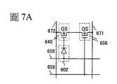
656:電晶體656: Transistor
658:光電二極體重設信號線658: photodiode reset signal line
659:閘極信號線659: Gate signal line
671:光電感測器輸出信號線671: Photoelectric sensor output signal line
672:光電感測器基準信號線672: photoelectric sensor reference signal line
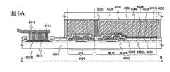
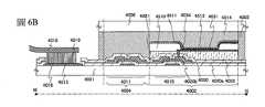
4001:基板4001: substrate
4002:像素部4002: Pixel section
4003:信號線驅動電路4003: signal line drive circuit
4004:掃描線驅動電路4004: Scan line drive circuit
4005:密封材料4005: Sealing material
4006:基板4006: substrate
4008:液晶層4008: liquid crystal layer
4010:電晶體4010: Transistor
4011:電晶體4011: Transistor
4013:液晶元件4013: liquid crystal element
4015:連接端子電極4015: Connect terminal electrode
4016:端子電極4016: terminal electrode
4018:FPC4018: FPC
4019:各向異性導電層4019: Anisotropic conductive layer
4020a:閘極絕緣層4020a: Gate insulation layer
4020b:氧化物絕緣層4020b: oxide insulating layer
4021:絕緣層4021: insulating layer
4030:氧化物絕緣層4030: oxide insulating layer
4031:電極層4031: electrode layer
4032:保護絕緣層4032: Protective insulation layer
4033:絕緣層4033: insulating layer
4034:電極層4034: Electrode layer
4035:間隔物4035: spacer
4038:絕緣層4038: insulating layer
4510:隔壁4510: next door
4511:電致發光層4511: Electroluminescent layer
4513:發光元件4513: light-emitting element
4514:填充材料4514: Filling material
9000:桌子9000: table
9001:外殼9001: Shell
9002:桌腿9002: table legs
9003:顯示部9003: Display
9004:顯示按鈕9004: Display button
9005:電源供應線9005: Power supply line
9033:卡子9033: clip
9034:開關9034: switch
9035:電源開關9035: Power switch
9036:開關9036: switch
9038:操作開關9038: Operation switch
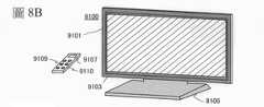
9100:電視機9100: TV
9101:外殼9101: Shell
9103:顯示部9103: Display
9105:支架9105: Bracket
9107:顯示部9107: Display
9109:操作鍵9109: Operation key
9110:遙控器9110: remote control
9201:主體9201: main body
9202:外殼9202: Shell
9203:顯示部9203: Display
9204:鍵盤9204: keyboard
9205:外部連接埠9205: External port
9206:指向裝置9206: pointing device
9630:外殼9630: Shell
9631:顯示部9631: Display
9631a:顯示部9631a: Display
9631b:顯示部9631b: Display
9632a:區域9632a: area
9632b:區域9632b: area
9633:太陽能電池9633: solar cell
9634:充放電控制電路9634: charge and discharge control circuit
9635:電池9635: battery
9636:DCDC轉換器9636: DCDC converter
9637:轉換器9637: converter
9638:操作鍵9638: Operation key
9639:按鈕9639: Button
在圖式中:In the schema:
圖1A至1C是示出半導體裝置的一個方式的平面圖及剖面圖;1A to 1C are plan views and cross-sectional views showing one mode of a semiconductor device;
圖2A至2C是示出半導體裝置的一個方式的平面圖及剖面圖;2A to 2C are plan views and cross-sectional views showing one mode of the semiconductor device;
圖3A至3D是示出半導體裝置的製造製程的一個例子的圖;3A to 3D are diagrams showing an example of a manufacturing process of a semiconductor device;
圖4A至4C是說明半導體裝置的一個方式的圖;4A to 4C are diagrams illustrating one mode of the semiconductor device;
圖5A和5B是說明半導體裝置的一個方式的圖;5A and 5B are diagrams illustrating one mode of the semiconductor device;
圖6A和6B是說明半導體裝置的一個方式的圖;6A and 6B are diagrams illustrating one mode of the semiconductor device;
圖7A和7B是說明半導體裝置的一個方式的圖;7A and 7B are diagrams illustrating one mode of the semiconductor device;
圖8A至8C是示出電子裝置的圖;8A to 8C are diagrams showing electronic devices;
圖9A至9C是示出電子裝置的圖:9A to 9C are diagrams showing electronic devices:
圖10A至10C是示出半導體裝置的一個方式的平面圖及剖面圖;10A to 10C are plan views and cross-sectional views showing one mode of the semiconductor device;
圖11A至11C是示出半導體裝置的一個方式的平面圖及剖面圖;11A to 11C are plan views and cross-sectional views showing one mode of the semiconductor device;
圖12A和12B是ESR測試的結果;Figures 12A and 12B are the results of the ESR test;
圖13A和13B是TDS測試的結果;Figures 13A and 13B are the results of the TDS test;
圖14是包含在本發明的一個方式的電晶體中的疊層結構的能帶圖。Fig. 14 is an energy band diagram of a laminated structure included in a transistor of one embodiment of the present invention.
下面,參照圖式詳細地說明本發明的實施模式。但是,所屬技術領域的普通技術人員可以很容易地理解一個事實,就是本發明的方式及詳細內容可以被變換為各種各樣的形式而不侷限於以下說明。從而,本發明不應被看作僅限定於以下實施模式的描述內容。Hereinafter, embodiments of the present invention will be described in detail with reference to the drawings. However, those of ordinary skill in the art can easily understand the fact that the mode and details of the present invention can be transformed into various forms without being limited to the following description. Therefore, the present invention should not be regarded as being limited only to the description of the following embodiment modes.
另外,在以下說明的本發明的結構中,在不同圖式之間共同使用同一符號表示同一部分或具有同樣功能的部分而省略其重複說明。此外,當表示具有相同功能的部分時有時使用相同的陰影線,而不特別附加元件符號。In addition, in the structure of the present invention described below, the same symbols are used in common between different drawings to denote the same parts or parts having the same functions, and repetitive descriptions thereof are omitted. In addition, the same hatching is sometimes used when indicating parts with the same function, and no symbol is particularly attached.
另外,在本說明書所說明的每個圖式中,每個結構的大小、膜的厚度或區域為了清晰可見而有時被誇大。因此,不一定侷限於其尺度。In addition, in each of the drawings described in this specification, the size of each structure, the thickness of the film, or the area is sometimes exaggerated in order to be clearly visible. Therefore, it is not necessarily limited to its scale.
在本說明書等中,為方便起見,附加了第一、第二等序數詞,這些序數詞並不表示製程順序或疊層順序。另外,這些序數詞在本說明書等中不表示用來特定發明的事項的固有名稱。In this specification, etc., for convenience, the ordinal numbers such as first and second are added, and these ordinal numbers do not indicate the process sequence or the stacking sequence. In addition, these ordinal numbers do not indicate the unique names of the matters used to specify the invention in this specification and the like.
實施模式1
在本實施模式中,參照圖1A至圖3D、以及圖10A至圖11C對半導體裝置及半導體裝置的製造方法的一個方式進行說明。在本實施模式中,作為半導體裝置的一個例子示出包含氧化物半導體層的底閘極型電晶體。In this embodiment mode, one aspect of a semiconductor device and a method of manufacturing the semiconductor device will be described with reference to FIGS. 1A to 3D and FIGS. 10A to 11C. In this embodiment mode, a bottom gate type transistor including an oxide semiconductor layer is shown as an example of a semiconductor device.
〈半導體裝置的結構例1〉<Semiconductor device structure example 1>
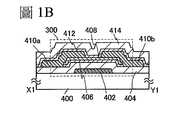
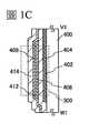
圖1A至1C示出電晶體300的結構實例。圖1A是電晶體300的平面圖,圖1B是沿著圖1A中的虛線X1-Y1的剖面圖,圖1C是沿著圖1A中的虛線V1-W1的剖面圖。1A to 1C show structural examples of the
電晶體300包含:設置在具有絕緣表面的基板400上的閘極電極層402;設置在閘極電極層402上的閘極絕緣層404;閘極絕緣層404上的氧化物絕緣層406;接觸於氧化物絕緣層406上並重疊於閘極電極層402的氧化物半導體層408;電連接到氧化物半導體層408的源極電極層410a及汲極電極層410b。The
在電晶體300中,閘極絕緣層404包含含有氮的矽膜而構成。與氧化矽膜相比,含有氮的矽膜的介電常數高,為了得到相等的靜電容量所需要的厚度大,所以可以在物理上加厚閘極絕緣層。從而,可以抑制電晶體300的絕緣耐壓的下降,進而可以藉由提高絕緣耐壓來抑制半導體裝置的靜電破壞。In the
將閘極絕緣層404的厚度至少設定為比氧化物絕緣層406厚,較佳的是,設定為325nm以上且550nm以下,更較佳為355nm以上且550nm以下。The thickness of the
例如,作為含有氮的矽膜可以舉出氮化矽膜、氮氧化矽膜、氧氮化矽膜。由於氮含量越多介電常數越高,所以採用氮化矽膜較佳。此外,由於與氧化矽的能隙8eV相比氮化矽的能隙低,為5.5eV,相應的固有電阻也低,所以藉由使用氮化矽膜可以賦予更高的耐ESD性能。另外,當利用CVD法形成氮化矽膜時,不需要使用在利用CVD法形成氮氧化矽膜等含有氧及氮的矽膜時使用的作為溫室效應氣體的N2O氣體。注意,在本說明書中,“氧氮化矽膜”是指在其組成中氧含量多於氮含量的膜,而“氮氧化矽膜”是指在其組成中氮含量多於氧含量的膜。For example, examples of the silicon film containing nitrogen include a silicon nitride film, a silicon oxynitride film, and a silicon oxynitride film. Since the higher the nitrogen content, the higher the dielectric constant, so it is better to use a silicon nitride film. In addition, since silicon nitride has a lower energy gap of 5.5 eV compared with the energy gap of silicon oxide of 8 eV, and the corresponding inherent resistance is also low, the use of a silicon nitride film can impart higher ESD resistance.In addition, when the silicon nitride film is formed by the CVD method, it is not necessary to use N 2 O gas, which is a greenhouse gas, which is used when a silicon film containing oxygen and nitrogen, such as a silicon oxynitride film, is formed by the CVD method. Note that in this specification, "silicon oxynitride film" refers to a film with more oxygen than nitrogen in its composition, and "silicon oxynitride film" refers to a film with more nitrogen than oxygen in its composition. .
在電晶體300中,氧化物絕緣層406包含含有從氧化物半導體層408的構成元素中選擇的一種或多種金屬元素而構成。藉由採用這種材料構成氧化物絕緣層406,可以使與氧化物半導體層408的介面穩定化,而能夠抑制電荷在該介面被捕獲。因此,可以防止電晶體的退化,尤其是光劣化,而能夠提供可靠性高的電晶體。In the
明確而言,作為氧化物絕緣層406,較佳為設置例如氧化鎵膜(也表示為GaOx。注意,x不侷限於自然數,包括非自然數)、氧化鎵鋅膜(也表示為Ga2ZnxOy(x=1至5))、Ga2O3(Gd2O3)膜、以及鎵的含量多且銦的含量少的絕緣性的In-Ga-Zn類氧化物膜等。Specifically, as the
也可以使氧化物絕緣層406和氧化物半導體層408的構成元素為相同,並使兩者的組成不同。例如,作為氧化物半導體層408,在使用In-Ga-Zn類氧化物半導體層的情況下,根據銦(In)和鎵(Ga)的比率,可以控制能隙,因此將氧化物半導體層408的原子數比設定為In:Ga:Zn=1:1:1或設定為In:Ga:Zn=3:1:2,將氧化物絕緣層406的原子數比設定為In:Ga:Zn=1:3:2,即可。注意,藉由濺射法可以形成氧化物絕緣層406及氧化物半導體層408,若濺射靶材含有銦,則可以減少成膜時的微粒的發生。因此,較佳為採用含有銦的氧化物絕緣層406及含有銦的氧化物半導體層408。The constituent elements of the
另外,在圖1A至1C的電晶體300中,表示藉由將氧化物半導體層408加工為島狀時的蝕刻處理,將氧化物絕緣層406也加工為島狀的例子。由此,氧化物半導體層408與氧化物絕緣層406的端部一致。In addition, the
以下說明氧化物半導體層的結構。The structure of the oxide semiconductor layer is explained below.
氧化物半導體層大致分為單晶氧化物半導體層和非單晶氧化物半導體層。非單晶氧化物半導體層包括非晶氧化物半導體層、微晶氧化物半導體層、多晶氧化物半導體層及CAAC-OS(C-Axis Aligned Crystalline Oxide Semiconductor:c軸配向結晶氧化物半導體)膜等。The oxide semiconductor layer is roughly divided into a single crystal oxide semiconductor layer and a non-single crystal oxide semiconductor layer.Crystalline oxide semiconductor layer. The non-single crystal oxide semiconductor layer includes an amorphous oxide semiconductor layer, a microcrystalline oxide semiconductor layer, a polycrystalline oxide semiconductor layer, and a CAAC-OS (C-Axis Aligned Crystalline Oxide Semiconductor) film Wait.
非晶氧化物半導體層具有無序的原子排列並不具有結晶成分。其典型例子是在微小區域中也不具有結晶部而膜整體具有完全的非晶結構的氧化物半導體層。The amorphous oxide semiconductor layer has a disordered atomic arrangement and does not have a crystalline component. A typical example of this is an oxide semiconductor layer that does not have crystal portions in a minute region, and the entire film has a complete amorphous structure.
微晶氧化物半導體層例如包括大於或等於1nm且小於10nm的尺寸的微晶(也稱為奈米晶)。因此,微晶氧化物半導體層的原子排列的有序度比非晶氧化物半導體層高。因此,微晶氧化物半導體層的缺陷態密度低於非晶氧化物半導體層。The microcrystalline oxide semiconductor layer includes, for example, microcrystals (also referred to as nanocrystals) having a size greater than or equal to 1 nm and less than 10 nm. Therefore, the order of the atomic arrangement of the microcrystalline oxide semiconductor layer is higher than that of the amorphous oxide semiconductor layer. Therefore, the density of defect states of the microcrystalline oxide semiconductor layer is lower than that of the amorphous oxide semiconductor layer.
CAAC-OS膜是包含多個結晶部的氧化物半導體層之一,大部分的結晶部為能夠容納在一邊短於100nm的立方體的尺寸。因此,有時包括在CAAC-OS膜中的結晶部為能夠容納在一邊短於10nm、短於5nm或短於3nm的立方體的尺寸。CAAC-OS膜的缺陷態密度低於微晶氧化物半導體層。下面,詳細說明CAAC-OS膜。The CAAC-OS film is one of the oxide semiconductor layers including a plurality of crystal parts, and most of the crystal parts have a size that can be accommodated in a cube whose one side is shorter than 100 nm. Therefore, sometimes the crystal portion included in the CAAC-OS film has a size that can be accommodated in a cube whose one side is shorter than 10 nm, shorter than 5 nm, or shorter than 3 nm. The defect state density of the CAAC-OS film is lower than that of the microcrystalline oxide semiconductor layer. Hereinafter, the CAAC-OS film will be described in detail.
在利用透射電子顯微鏡(TEM:Transmission Electron Microscope)所得到的CAAC-OS膜的影像中,不能明確地觀察到結晶部與結晶部之間的邊界,即晶界(grain boundary)。因此,在CAAC-OS膜中,不容易產生起因於晶界的電子遷移率的降低。In the image of the CAAC-OS film obtained by a transmission electron microscope (TEM: Transmission Electron Microscope), the boundary between the crystal part and the crystal part, that is, the grain boundary, cannot be clearly observed. Therefore, in the CAAC-OS film, a decrease in electron mobility due to grain boundaries is not likely to occur.
由從大致平行於樣本面的方向利用TEM所得到的CAAC-OS膜的影像(剖面TEM影像)可知,在結晶部中金屬原子排列為層狀。各金屬原子層具有反映被形成CAAC-OS膜的面(也稱為被形成面)或CAAC-OS膜的頂面的凸凹的形狀並以平行於CAAC-OS膜的被形成面或頂面的方式排列。Obtained by using TEM from a direction roughly parallel to the sample surfaceThe image of the CAAC-OS film (cross-sectional TEM image) shows that the metal atoms are arranged in layers in the crystal part. Each metal atomic layer has a shape that reflects the surface on which the CAAC-OS film is formed (also referred to as the formed surface) or the convex and concave shape of the top surface of the CAAC-OS film, and is parallel to the formed surface or top surface of the CAAC-OS film Way to arrange.
在本說明書中,“平行”是指在-10°以上且10°以下的角度的範圍中配置兩條直線的狀態,因此也包括-5°以上且5°以下的角度的狀態。另外,“垂直”是指在80°以上且100°以下的角度的範圍中配置兩條直線的狀態,因此也包括85°以上且95°以下的角度的狀態。In this specification, "parallel" refers to a state where two straight lines are arranged in an angle range of -10° or more and 10° or less, and therefore also includes a state where an angle of -5° or more and 5° or less is included. In addition, "perpendicular" refers to a state where two straight lines are arranged in an angle range of 80° or more and 100° or less, and therefore also includes a state where an angle of 85° or more and 95° or less is included.
另一方面,由從大致垂直於樣本面的方向利用TEM所得到的CAAC-OS膜的影像(平面TEM影像)可知,在結晶部中金屬原子排列為三角形狀或六角形狀。但是,在不同的結晶部之間沒有確認到金屬原子的排列的有序性。On the other hand, an image of the CAAC-OS film (planar TEM image) obtained by TEM from a direction substantially perpendicular to the sample surface shows that the metal atoms are arranged in a triangular shape or a hexagonal shape in the crystal portion. However, the orderliness of the arrangement of metal atoms was not confirmed between different crystal parts.
由剖面TEM影像及平面TEM影像可知,CAAC-OS膜的結晶部具有配向性。It can be seen from the cross-sectional TEM image and the planar TEM image that the crystalline part of the CAAC-OS film has orientation.
使用X射線繞射(XRD:X-Ray Diffraction)裝置對CAAC-OS膜進行結構分析。例如,在藉由out-of-plane法分析包括InGaZnO4的結晶的CAAC-OS膜的情況下,在繞射角度(2θ)為31°附近有時出現峰值。由於該峰值歸屬於InGaZnO4結晶的(009)面,所以可以確認到CAAC-OS膜的結晶具有c軸配向性並且c軸在大致垂直於CAAC-OS膜的被形成面或頂面的方向上配向。X-ray diffraction (XRD: X-Ray Diffraction) device was used to analyze the structure of the CAAC-OS film. For example, in the case of analyzinga CAAC-OS film including crystals of InGaZnO 4 by the out-of-plane method, a peak sometimes appears when the diffraction angle (2θ) is around 31°. Since this peak is attributed tothe (009) plane of the InGaZnO 4 crystal, it can be confirmed that the crystal of the CAAC-OS film has c-axis orientation and the c-axis is in a direction substantially perpendicular to the formed surface or top surface of the CAAC-OS film Alignment.
另一方面,在藉由從大致垂直於c軸的方向使X線入射到樣本的in-plane法分析CAAC-OS膜的情況下,在2θ為56°附近有時出現峰值。該峰值歸屬於InGaZnO4結晶的(110)面。在此,假設樣本是InGaZnO4的單晶氧化物半導體層,在將2θ固定為56°附近的狀態下,一邊以樣本面的法線向量為軸(


由上述結果可知,在具有c軸配向的CAAC-OS膜中,雖然a軸及b軸的方向在結晶部之間不同,但是c軸在平行於被形成面或頂面的法線向量的方向上配向。因此,在上述剖面TEM影像中觀察到的排列為層狀的各金屬原子層相當於平行於結晶的ab面的面。From the above results, it can be seen that in the CAAC-OS film with c-axis alignment, although the directions of the a-axis and the b-axis are different between the crystal parts, the c-axis is in the direction parallel to the normal vector of the surface to be formed or the top surface.上Alignment. Therefore, each metal atom layer arranged in a layered shape observed in the cross-sectional TEM image corresponds to a plane parallel to the ab plane of the crystal.
注意,結晶部在形成CAAC-OS膜或進行加熱處理等晶化處理時形成。如上所述,結晶的c軸在平行於CAAC-OS膜的被形成面或頂面的法線向量的方向上配向。由此,例如,在藉由蝕刻等改變CAAC-OS膜的形狀的情況下,有時結晶的c軸未必平行於CAAC-OS膜的被形成面或頂面的法線向量。Note that the crystal portion is formed when the CAAC-OS film is formed or when crystallization treatment such as heat treatment is performed. As described above, the c-axis of the crystal is aligned in a direction parallel to the normal vector of the formed surface or the top surface of the CAAC-OS film. Therefore, for example, when the shape of the CAAC-OS film is changed by etching or the like, the c-axis of the crystal may not necessarily be parallel to the normal vector of the formed surface or the top surface of the CAAC-OS film.
此外,CAAC-OS膜中的晶化度未必均勻。例如,在CAAC-OS膜的結晶部藉由從CAAC-OS膜的頂面近旁產生的結晶生長而形成的情況下,有時頂面附近的區域的晶化度高於被形成面附近的區域。另外,在對CAAC-OS膜添加雜質時,被添加雜質的區域的晶化度變化,有時部分性地形成晶化度不同的區域。In addition, the degree of crystallization in the CAAC-OS film is not necessarily uniform. For example, in the case where the crystal portion of the CAAC-OS film is formed by crystal growth from the vicinity of the top surface of the CAAC-OS film, the crystallinity of the region near the top surface may be higher than the region near the surface to be formed . In addition, adding to the CAAC-OS filmWhen impurities are added, the crystallinity of the region to which the impurity is added changes, and sometimes regions with different crystallinity are partially formed.
注意,在藉由out-of-plane法分析包括InGaZnO4結晶的CAAC-OS膜的情況下,除了2θ為31°附近的峰值之外,有時還觀察到2θ為36°附近的峰值。2θ為36°附近的峰值示出不具有c軸配向性的結晶包括在CAAC-OS膜的一部分中。較佳的是,CAAC-OS膜在2θ為31°附近出現峰值並在2θ為36°附近不出現峰值。Note that in the case of analyzing the CAAC-OS film including InGaZnO 4 crystals by the out-of-plane method, in addition to the peak near 31° in 2θ, a peak near 36° in 2θ is sometimes observed. The peak of 2θ in the vicinity of 36° indicates that crystals having no c-axis alignment are included in a part of the CAAC-OS film. Preferably, the CAAC-OS film has a peak around 31° 2θ and no peak around 36° 2θ.
在本說明書中,六方晶系包括三方晶系和菱方晶系。In this specification, the hexagonal crystal system includes the trigonal crystal system and the rhombohedral crystal system.
在使用CAAC-OS膜的電晶體中,起因於可見光或紫外光的照射的電特性的變動小。因此,該電晶體具有高可靠性。In the transistor using the CAAC-OS film, the change in electrical characteristics due to irradiation of visible light or ultraviolet light is small. Therefore, the transistor has high reliability.
注意,氧化物半導體層408例如為包括非晶氧化物半導體層、微晶氧化物半導體層和CAAC-OS膜中的任何一個的結構,也可以為它們的混合膜。另外,也可以是上述中的兩種以上的疊層膜。Note that the
另外,與氧化物半導體層408相比,有時氧化物絕緣層406的結晶性低。例如,有時氧化物絕緣層406包括非晶部或奈米晶。In addition, the
作為電晶體300的構成要素,也可以包括覆蓋源極電極層410a及汲極電極層410b並接觸於氧化物半導體層408的氧化物絕緣層412及/或氧化物絕緣層412上的保護絕緣層414。As a constituent element of the
作為氧化物絕緣層412,與氧化物絕緣層406同樣,較佳為使用從氧化物半導體層408的構成元素中選擇的一種或多種金屬元素構成的層。藉由採用這種材料,可以使氧化物絕緣層412和氧化物半導體層408之間的介面穩定化。因為氧化物絕緣層412是接觸於氧化物半導體層408的背通道一側的絕緣層,所以藉由抑制該兩層之間的介面上的電荷捕獲,能夠抑制寄生通道的發生。As the
此外,藉由以夾著氧化物半導體層408的方式設置含有從氧化物半導體層的構成元素中選擇的一種或多種金屬元素的氧化物絕緣層,有阻擋對氧化物半導體層造成影響的雜質(例如氮或金屬元素等)從外部擴散並侵入的功能。由此,藉由以夾著氧化物半導體層或圍繞氧化物半導體層的方式設置該氧化物絕緣層,可以將被圍繞的氧化物半導體層的組成及純度保持為一定,而能夠實現具有穩定的電特性的半導體裝置。In addition, by providing an oxide insulating layer containing one or more metal elements selected from the constituent elements of the oxide semiconductor layer so as to sandwich the
作為保護絕緣層414,可以使用氧化矽膜、氧化鎵膜、氧化鋁膜、氮化矽膜、氧氮化矽膜、氧氮化鋁膜或氮氧化矽膜等。As the protective insulating
〈半導體裝置的結構例2〉<Semiconductor device structure example 2>
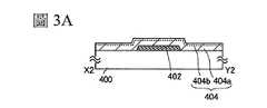
圖2A至2C示出電晶體310的結構例。圖2A是電晶體310的平面圖,圖2B是沿著圖2A中的虛線X2-Y2的剖面圖,圖2C是沿著圖2A的虛線V2-W2的剖面圖。2A to 2C show structural examples of the
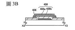
與圖1A至1C的電晶體300同樣,圖2A至2C所示的電晶體310包括:設置在具有絕緣表面的基板400上的閘極電極層402;設置在閘極電極層402上的閘極絕緣層404;閘極絕緣層404上的氧化物絕緣層406;接觸於氧化物絕緣層406上並重疊於閘極電極層402的氧化物半導體層408;電連接到氧化物半導體層408的源極電極層410a及汲極電極層410b。此外也可以作為電晶體310的構成要素包含覆蓋源極電極層410a及汲極電極410b並接觸於氧化物半導體層408的氧化物絕緣層412、以及氧化物絕緣層412上的保護絕緣層414。Like the
電晶體310中的閘極絕緣層404和氧化物半導體層408的結構與電晶體300中的結構不同。就是說,在電晶體310中閘極絕緣層404包含接觸於閘極電極層402的閘極絕緣層404a及設置在閘極絕緣層404a和氧化物絕緣層406之間的閘極絕緣層404b而構成。此外,在電晶體310中,氧化物半導體層408包含接觸於氧化物絕緣層406的氧化物半導體層408a及接觸於氧化物絕緣層412的氧化物半導體層408b而構成。另外,在電晶體310中,閘極絕緣層404及氧化物半導體層408之外的結構與電晶體300的結構相同,可以參考電晶體300的說明。The structures of the
在電晶體310中,閘極絕緣層404a及閘極絕緣層404b包含氮化矽膜。In the
閘極絕緣層404a包含比閘極絕緣層404b厚度大且膜中缺陷少的氮化矽膜。例如,將閘極絕緣層404a的厚度設定為300nm以上且400nm以下。另外,對應於在電子自旋共振(ESR:Electron Spin Resonance)法中在Nc中心(g值為2.003)出現的信號的自旋密度較佳為1×10¹⁷spins/cm3以下,更較佳為5×1016spins/cm3以下的氮化矽膜。如此,藉由作為閘極絕緣層404a使用膜中缺陷少且厚度大(例如,300nm以上)的氮化矽膜,例如可以將閘極絕緣層404a的耐耐受電壓值提高到300V以上。The
另外,由於閘極絕緣層404b與氧化物半導體層408接觸,所以作為閘極絕緣層404b使用含有氫濃度低的氮化矽膜,該氫濃度至少低於閘極絕緣層404a的氫濃度。例如,在利用電漿CVD法形成閘極絕緣層404a及閘極絕緣層404b的情況下,藉由降低供應氣體中的氫濃度,可以使閘極絕緣層404b的氫濃度低於閘極絕緣層404a。明確而言,當作為閘極絕緣層404a及閘極絕緣層404b形成氮化矽時,使用來形成閘極絕緣層404b的供應氣體中的氨流量低於用來形成閘極絕緣層404a的供應氣體中的氨流量,或者在不使用氨的情況下形成閘極絕緣層404b即可。In addition, since the
另外,將閘極絕緣層404b的厚度設定為25nm以上且150nm以下。作為閘極絕緣層404b設置氫濃度低的氮化矽膜,這樣可以抑制氫或氫化合物(例如,水)混入氧化物絕緣層406及氧化物半導體層408。由於在氧化物半導體中氫為載流子生成要因而有可能使電晶體的臨界電壓向負漂移(shift),所以藉由作為閘極絕緣層404b設置氫濃度低的氮化矽膜,可以使電晶體的電特性穩定化。另外,藉由作為閘極絕緣層404b設置氫濃度低的氮化矽膜,閘極絕緣層404b還用作防止閘極絕緣層404a所含有的氫或氫化合物等雜質擴散到氧化物絕緣層406及氧化物半導體層408中的障壁膜。In addition, the thickness of the
另外,在本實施模式中,由於閘極絕緣層404a及閘極絕緣層404b都是氮化矽膜,所以有時根據材料和成膜條件閘極絕緣層之間的介面不明確。因此,在圖2B和2C中,示意性地以虛線示出閘極絕緣層404a與閘極絕緣層404b之間的介面。這在下面的各圖式中也是同樣的。In addition, in this embodiment mode, since the
較佳的是,將包含在氧化物半導體層408中的氧化物半導體層408a和氧化物半導體層408b的構成元素設定為相同,並使兩者的組成不同。在作為氧化物半導體層408a及氧化物半導體層408b形成包含銦及鎵的氧化物半導體層的情況下,較佳的是,將離閘極電極層402近的一側(通道一側)的氧化物半導體層408a的銦及鎵的含量比設定為In>Ga。此外,較佳的是,將離閘極電極層402遠的一側(背通道一側)的氧化物半導體層408b的銦及鎵的含量比設定為In
在氧化物半導體中,重金屬的s軌道有助於載流子傳導,藉由增加銦的含量比呈現增加s軌道的重疊率的傾向,由此具有In>Ga的組成的氧化物的遷移率比具有In

藉由在通道一側使用具有In>Ga的組成的氧化物半導體並在背通道一側使用具有In
另外,將接觸於氧化物半導體層408a的氧化物絕緣層406的構成元素設定為與氧化物半導體層408a相同,並使兩者的組成不同,當對氧化物絕緣層406賦予絕緣性時,能夠使兩者的介面進一步穩定化,所以這是較佳的。接觸於氧化物半導體層408b的氧化物絕緣層412也是同樣的。In addition, the constituent elements of the
另外,對氧化物半導體層408a及氧化物半導體層408b也可以使用結晶性不同的氧化物半導體。就是說,也可以採用適當地組合單晶氧化物半導體、多晶氧化物半導體、奈米晶氧化物半導體、非晶氧化物半導體或CAAC-OS的結構。另一方面,非晶氧化物半導體容易吸收氫等雜質,並且,容易產生氧缺陷而容易成為n型化。由此,通道一側的氧化物半導體層408a較佳為使用CAAC-OS等具有結晶性的氧化物半導體。In addition, oxide semiconductors with different crystallinities may be used for the
此外,當對背通道一側的氧化物半導體層408b使用非晶氧化物半導體時,由於形成源極電極層410a及汲極電極層410b時的蝕刻處理發生氧缺陷,而容易被n型化。因此,對氧化物半導體層408b較佳為使用具有晶性的氧化物半導體。In addition, when an amorphous oxide semiconductor is used for the
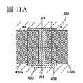
圖14是在本實施模式的電晶體中層疊閘極絕緣層GI、氧化物絕緣層OI1、氧化物半導體層OS1、OS2、氧化物絕緣層OI2、以及保護絕緣層Passi的結構中的能帶圖(模式圖)。在圖14中假設閘極絕緣層、氧化物絕緣層、氧化物半導體層及保護絕緣層都為理想的本質狀態,並且示出作為閘極絕緣層GI及保護絕緣層Passi使用氮化矽膜(帶隙Eg為5eV);作為氧化物絕緣層OI1及氧化物絕緣層OI2使用In:Ga:Zn=1:3:2的In-Ga-Zn類氧化物絕緣層(帶隙Eg為3.6eV);作為氧化物半導體層OS1使用In:Ga:Zn=3:1:2的In-Ga-Zn類氧化物半導體層(帶隙Eg為2.8eV);以及作為氧化物半導體層OS2使用In:Ga:Zn=1:1:1的In-Ga-Zn類氧化物半導體層(帶隙Eg為3.2eV)的情況。14 is an energy band diagram in the structure in which the gate insulating layer GI, the oxide insulating layer OI1, the oxide semiconductor layers OS1, OS2, the oxide insulating layer OI2, and the protective insulating layer Passi are stacked in the transistor of this embodiment mode (Schematic diagram). It is assumed in FIG. 14 that the gate insulating layer, the oxide insulating layer, the oxide semiconductor layer, and the protective insulating layer are all in an ideal essential state, and it is shown that a silicon nitride film is used as the gate insulating layer GI and the protective insulating layer Passi ( The band gap Eg is 5eV); as the oxide insulating layer OI1 and the oxide insulating layer OI2, an In-Ga-Zn based oxide insulating layer of In:Ga:Zn=1:3:2 is used (the band gap Eg is 3.6eV) ; As the oxide semiconductor layer OS1, In-Ga-Zn-based oxide semiconductor layer of In:Ga:Zn=3:1:2 (band gap Eg is 2.8eV) is used; and In:Ga is used as the oxide semiconductor layer OS2 : In the case of an In-Ga-Zn-based oxide semiconductor layer of Zn=1:1:1 (band gap Eg is 3.2 eV).
另外,在圖14中將氧化物絕緣層OI1、氧化物絕緣層OI2、氧化物半導體層OS1及氧化物半導體層OS2的介電常數都假設為15。另外,將氧化物絕緣層OI1及氧化物絕緣層OI2的遷移率設定為4cm2/Vs,將氧化物半導體層OS1的遷移率設定為25cm2/Vs,以及將氧化物半導體層OS2的遷移率設定為10cm2/Vs。此外,將閘極絕緣層GI的厚度設定為325nm,將氧化物絕緣層OI1的厚度設定為30nm,將氧化物半導體層OS1的厚度設定為10nm,將氧化物半導體層OS2的厚度設定為10nm,將氧化物絕緣層OI2的厚度設定為30nm,以及將保護絕緣層Passi的厚度設定為300nm而進行計算。In addition, in FIG. 14, the dielectric constants of the oxide insulating layer OI1, the oxide insulating layer OI2, the oxide semiconductor layer OS1, and the oxide semiconductor layer OS2 are all assumed to be 15. In addition, the mobility of the oxide insulating layer OI1 and the oxide insulating layer OI2 is set to 4 cm2 /Vs, the mobility of the oxide semiconductor layer OS1 is set to 25 cm2 /Vs, and the mobility of the oxide semiconductor layer OS2 is set to Set to 10cm2 /Vs. In addition, the thickness of the gate insulating layer GI is set to 325 nm, the thickness of the oxide insulating layer OI1 is set to 30 nm, the thickness of the oxide semiconductor layer OS1 is set to 10 nm, and the thickness of the oxide semiconductor layer OS2 is set to 10 nm. The calculation is performed by setting the thickness of the oxide insulating layer OI2 to 30 nm and the thickness of the protective insulating layer Passi to 300 nm.
如圖14所示,在氧化物半導體層OS1的閘極電極一側(通道一側),氧化物半導體層OS1和氧化物絕緣層OI1之間的介面存在有勢壘。與此同樣,在氧化物半導體層OS2的背通道一側(與閘極電極相反一側),氧化物半導體層OS2和氧化物絕緣層OI2之間的介面存在有勢壘。因在氧化物半導體層和氧化物絕緣層之間的介面有這種勢壘,阻礙載流子在該介面移動,所以載流子不從氧化物半導體層中移動到氧化物絕緣層中,而在氧化物半導體層中移動。就是說,藉由使用與氧化物半導體相比其帶隙分階段地增大的材料來夾著氧化物半導體層而形成疊層結構,載流子在氧化物半導體層OS1及氧化物半導體層OS2中移動。As shown in FIG. 14, on the gate electrode side (channel side) of the oxide semiconductor layer OS1, there is a potential barrier at the interface between the oxide semiconductor layer OS1 and the oxide insulating layer OI1. Similarly, on the back channel side of the oxide semiconductor layer OS2 (the side opposite to the gate electrode), there is a potential barrier at the interface between the oxide semiconductor layer OS2 and the oxide insulating layer OI2. Since there is such a potential barrier at the interface between the oxide semiconductor layer and the oxide insulating layer, which hinders the movement of carriers on this interface, the carriers do not move from the oxide semiconductor layer to the oxide insulating layer, and Move in the oxide semiconductor layer. In other words, by sandwiching the oxide semiconductor layer by using a material whose band gap is gradually larger than that of an oxide semiconductor, a stacked structure is formed, and carriers are formed in the oxide semiconductor layer OS1 and the oxide semiconductor layer OS2. Moving in.
〈半導體裝置的製造方法〉<Method of Manufacturing Semiconductor Device>
圖3A至3D示出電晶體310的製造方法的一個例子。3A to 3D show an example of a method of manufacturing the
首先,在具有絕緣表面的基板400上形成閘極電極層402。First, a
對可用作具有絕緣表面的基板400的基板沒有特別的限制,但是基板400需要至少具有能夠承受在後面進行的加熱處理的程度的耐熱性。例如,可以使用諸如硼矽酸鋇玻璃和硼矽酸鋁玻璃等玻璃基板、陶瓷基板、石英基板、藍寶石基板等。另外,作為基板400,可以採用以矽或碳化矽等為材料的單晶半導體基板或多晶半導體基板、以矽鍺為材料的化合物半導體基板、SOI基板等,並且也可以使用在這些基板上設置有半導體元件的基板。There is no particular limitation on the substrate that can be used as the
閘極電極層402可以使用鉬、鈦、鉭、鎢、鋁、銅、鉻、釹、鈧等金屬材料或以上述金屬材料為主要成分的合金材料。此外,閘極電極層402可以使用以摻雜有磷等雜質元素的多晶矽膜為代表的半導體膜、鎳矽化物等矽化物膜。閘極電極層402既可以是單層結構,又可以是疊層結構。也可以使閘極電極層402具有錐形形狀,例如可以將錐角設定為30°以上且70°以下。在此,錐角是指具有錐形形狀的層的側面與該層的底面之間的角度。For the
另外,作為閘極電極層402的材料還可以使用氧化銦氧化錫、含有氧化鎢的氧化銦、含有氧化鎢的氧化銦鋅、含有氧化鈦的氧化銦、含有氧化鈦的氧化銦錫、氧化銦氧化鋅、添加有氧化矽的氧化銦錫等導電材料。In addition, as the material of the
或者,作為閘極電極層402的材料還可以使用含有氮的In-Ga-Zn類氧化物、含有氮的In-Sn類氧化物、含有氮的In-Ga類氧化物、含有氮的In-Zn類氧化物、含有氮的Sn類氧化物、含有氮的In類氧化物、金屬氮化物膜(氮化銦、氮化鋅、氮化鉭、氮化鎢等)。由於上述材料具有5eV以上的功函數,所以藉由使用上述材料形成閘極電極層402,可以使電晶體的臨界電壓成為正值,由此可以實現常截止(normally-off)的開關電晶體。Alternatively, as the material of the
接著,以覆蓋閘極電極層402的方式形成包含閘極絕緣層404a及閘極絕緣層404b的閘極絕緣層404(參照圖3A)。閘極絕緣層404可以採用含有氮的矽膜。在本實施模式中,層疊由氮化矽膜構成的閘極絕緣層404a與由氮化矽膜構成的閘極絕緣層404b而形成閘極絕緣層404。從降低面內的不均勻性、微粒的混入以及成膜時間(節拍時間)的觀點來看,有效的是利用CVD法形成閘極絕緣層404。另外,當在大面積基板上進行成膜的情況下CVD法也是有效的。Next, a gate insulating layer is formed so as to cover the
在本實施模式中,利用電漿CVD法連續地形成閘極絕緣層404a及閘極絕緣層404b。首先,在以矽烷(SiH4)、氮(N2)及氨(NH3)的混合氣體為供應氣體的狀態下形成用作閘極絕緣層404a的氮化矽膜,然後將供應氣體轉換為矽烷(SiH4)與氮(N2)的混合氣體並形成用作閘極絕緣層404b的氮化矽膜。In this embodiment mode, the
在以矽烷(SiH4)、氮(N2)及氨(NH3)的混合氣體為電漿CVD法的供應氣體的狀態下形成的氮化矽膜的膜中缺陷少於在以矽烷(SiH4)與氮(N2)的混合氣體為供應氣體的狀態下形成的氮化矽膜。因此,閘極絕緣層404a的膜中缺陷至少少於閘極絕緣層404b。例如,可以將對應於在電子自旋共振(ESR)法中在Nc中心(g值為2.003)出現的信號的自旋密度設定為1×10¹⁷spins/cm3以下較佳,更較佳的是,設定為5×1016spins/cm3以下。另外,由於在混合氣體含有氨的狀態下形成的氮化矽膜與以矽烷與氮的混合氣體為供應氣體的情況相比具有更高的覆蓋性,所以作為與閘極電極層402接觸的閘極絕緣層設置使用上述混合氣體而形成的氮化矽膜是有效的。另外,藉由作為閘極絕緣層404a使用膜中缺陷少且厚度為300nm以上且400nm以下的氮化矽膜,可以將閘極絕緣層404a的耐受電壓提高到300V以上。The silicon nitride film formed under the condition that the mixed gas of silane (SiH4 ), nitrogen (N2 ) and ammonia (NH3 ) is used as the supply gas of the plasma CVD method has fewer defects than the silicon nitride (SiH 4) film.4 ) A silicon nitride film formed in a state where a mixed gas of nitrogen (N2) is a supplied gas. Therefore, the defects in the film of the
另外,在材料氣體不含有氨的情況下形成的閘極絕緣層404b的氫濃度比閘極絕緣層404a低。藉由將這種膜的厚度設定為25nm以上且150nm以下並設置在氧化物絕緣層406和閘極電極層402之間,可以抑制氫從閘極絕緣層404b混入氧化物絕緣層406及氧化物半導體層408。另外,閘極絕緣層404b還用作防止閘極絕緣層404a所含有的氫或氫化合物混入到氧化物絕緣層406及氧化物半導體層408中的障壁膜。In addition, the
藉由作為閘極絕緣層404層疊膜中缺陷少且厚度大的閘極絕緣層404a與氫濃度低的閘極絕緣層404b,在改善絕緣耐壓的同時可以抑制氫等雜質擴散到氧化物絕緣層406及氧化物半導體層408中。由此,可以抑制包含該閘極絕緣層404的電晶體的靜電破壞,並且可以使電特性穩定化。By using the
接著,在閘極絕緣層404b上形成氧化物絕緣層及氧化物半導體層並利用蝕刻處理將其加工為島狀來形成氧化物絕緣層406、包括氧化物半導體層408a及氧化物半導體層408b的氧化物半導體層408(參照圖3B)。該蝕刻處理可以使用同一個光遮罩來進行,因此從平面看時的氧化物絕緣層406和氧化物半導體層408的圖案形狀為相同,且端部一致。Next, an oxide insulating layer and an oxide semiconductor layer are formed on the
作為氧化物絕緣層406設置含有從氧化物半導體層408的構成元素中選擇的一種或多種金屬元素的氧化物絕緣層。例如,較佳的是,使用氧化鎵膜、氧化鎵鋅膜、氧化鎵釓膜、或鎵的含量多且銦的含量少的絕緣性的In-Ga-Zn類氧化物膜等的絕緣膜。As the
氧化物半導體層408既可以具有非晶結構又可以具有結晶性。在使成膜之後的氧化物半導體層具有非晶結構的情況下,可以藉由在後面的製造製程中進行加熱處理來形成具有結晶性的氧化物半導體層408。用來使該非晶氧化物半導體層結晶化的加熱處理的溫度為250℃以上且700℃以下,較佳為400℃以上,更較佳為500℃以上,進一步較佳為550℃以上。另外,該加熱處理也可以兼作製造製程中的其他加熱處理。The
作為氧化物絕緣層406及氧化物半導體層408的成膜方法,可以適當地利用濺射法、MBE(Molecular Beam Epitaxy:分子束磊晶)法、CVD法、脈衝雷射沉積法、ALD(Atomic Layer Deposition:原子層沉積)法等。As a method of forming the
當形成氧化物絕緣層406及氧化物半導體層408時,盡可能地降低膜中的氫濃度較佳。為了降低氫濃度,例如,在藉由濺射法進行成膜時,作為供應到濺射裝置的成膜室內的氛圍氣體適當地使用:如氫、水、羥基或者氫化物等雜質被去除的高純度的稀有氣體(典型的有氬)、氧、稀有氣體和氧的混合氣體。When forming the
另外,藉由在去除殘留在成膜室內的水分的同時引入去除了氫及水分的濺射氣體來進行成膜,可以降低所形成的氧化物絕緣層及氧化物半導體層的氫濃度。為了去除殘留在成膜室內的水分,較佳為使用吸附型真空泵,例如,低溫泵、離子泵、鈦昇華泵。此外,也可以使用具備冷阱的渦輪泵。由於低溫泵對如氫分子、水(H2O)等包含氫原子的化合物(還包括包含碳原子的化合物較佳)等進行排出的能力較高,所以可以降低在利用低溫泵進行了排氣的成膜室中形成的膜中的雜質濃度。In addition, by introducing a sputtering gas from which hydrogen and moisture have been removed to perform film formation while removing moisture remaining in the film formation chamber, the hydrogen concentration of the formed oxide insulating layer and oxide semiconductor layer can be reduced. In order to remove the moisture remaining in the film forming chamber, it is preferable to use an adsorption-type vacuum pump, for example, a cryopump, an ion pump, or a titanium sublimation pump. In addition, a turbo pump equipped with a cold trap can also be used. Since the cryopump has a high ability to discharge compounds containing hydrogen atoms such as hydrogen molecules and water (H2 O) (compounds containing carbon atoms are also preferred), it can reduce the use of cryopumps for exhaust The impurity concentration in the film formed in the film forming chamber.
另外,較佳的是,以不暴露於大氣的方式連續地形成氧化物絕緣層和氧化物半導體層。藉由以不暴露於大氣的方式連續地形成氧化物絕緣層和氧化物半導體層,可以防止氫或氫化合物(例如,吸著的水等)附著於氧化物絕緣層表面或層疊的氧化物半導體層表面,所以可以抑制雜質的混入。In addition, it is preferable to continuously form the oxide insulating layer and the oxide semiconductor layer without being exposed to the atmosphere. By continuously forming the oxide insulating layer and the oxide semiconductor layer without being exposed to the atmosphere, it is possible to prevent hydrogen or hydrogen compounds (for example, adsorbed water, etc.) from adhering to the surface of the oxide insulating layer or the laminated oxide semiconductor The surface of the layer, so the mixing of impurities can be suppressed.
另外,在藉由濺射法形成氧化物絕緣層或氧化物半導體層的情況下,使用於成膜的金屬氧化物靶材的相對密度(填充率)為90%以上且100%以下,較佳為95%以上且99.9%以下。藉由使用相對密度高的金屬氧化物靶材,可以形成緻密的膜。In addition, in the case of forming an oxide insulating layer or an oxide semiconductor layer by a sputtering method, the relative density (filling rate) of the metal oxide target used for film formation is 90% or more and 100% or less, preferably It is 95% or more and 99.9% or less. By using a relatively high-density metal oxide target, a dense film can be formed.
另外,為了降低有可能包含在氧化物半導體層中的雜質的濃度,在將基板400保持為高溫的狀態下形成氧化物半導體層也是有效的。將加熱基板400的溫度設定為150℃以上且450℃以下,較佳的是,將基板溫度設定為200℃以上且350℃以下即可。另外,藉由在進行成膜時以高溫加熱基板,可以形成結晶氧化物半導體層。In addition, in order to reduce the concentration of impurities that may be contained in the oxide semiconductor layer, it is also effective to form the oxide semiconductor layer while maintaining the
當作為氧化物半導體層408使用CAAC-OS膜時,作為獲得該CAAC-OS膜的方法,例如可以將成膜溫度設定為200℃以上且450℃以下來形成氧化物半導體層,而實現大致垂直於其表面的c軸配向。或者,也可以在形成薄的氧化物半導體層之後,進行200℃以上且700℃以下的加熱處理,而實現大致垂直於其表面的c軸配向。或者,也可以在形成薄的第一層之後,進行200℃以上且700℃以下的加熱處理,然後形成第二層,而實現大致垂直於其表面的c軸配向。When a CAAC-OS film is used as the
用於氧化物半導體層408的氧化物半導體至少含有銦(In)。尤其較佳為含有銦及鋅(Zn)。此外,作為用來減小使用該氧化物半導體的電晶體的電特性的不均勻的穩定劑(stabilizer),較佳為除了上述元素以外還含有鎵(Ga)。此外,作為穩定劑較佳為含有錫(Sn)、鉿(Hf)、鋁(Al)和鋯(Zr)中的一種或多種。The oxide semiconductor used for the
另外,作為其他穩定劑,也可以含有鑭系元素的鑭(La)、鈰(Ce)、鐠(Pr)、釹(Nd)、釤(Sm)、銪(Eu)、釓(Gd)、鋱(Tb)、鏑(Dy)、鈥(Ho)、鉺(Er)、銩(Tm)、鐿(Yb)、鑥(Lu)中的一種或多種。In addition, as other stabilizers, lanthanum (La), cerium (Ce), samarium (Pr), neodymium (Nd), samarium (Sm), europium (Eu), gamma (Gd), and pomium can also be contained as other stabilizers. One or more of (Tb), dysprosium (Dy), 鈥 (Ho), erbium (Er), 銩 (Tm), ytterbium (Yb), and 鑥 (Lu).
例如,作為氧化物半導體,可以使用:氧化銦、氧化錫、氧化鋅;二元金屬氧化物的In-Zn類氧化物、In-Mg類氧化物、In-Ga類氧化物;三元金屬氧化物的In-Ga-Zn類氧化物、In-Al-Zn類氧化物、In-Sn-Zn類氧化物、In-Hf-Zn類氧化物、In-La-Zn類氧化物、In-Ce-Zn類氧化物、In-Pr-Zn類氧化物、In-Nd-Zn類氧化物、In-Sm-Zn類氧化物、In-Eu-Zn類氧化物、In-Gd-Zn類氧化物、In-Tb-Zn類氧化物、In-Dy-Zn類氧化物、In-Ho-Zn類氧化物、In-Er-Zn類氧化物、In-Tm-Zn類氧化物、In-Yb-Zn類氧化物、In-Lu-Zn類氧化物;以及四元金屬氧化物的In-Sn-Ga-Zn類氧化物、In-Hf-Ga-Zn類氧化物、In-Al-Ga-Zn類氧化物、In-Sn-Al-Zn類氧化物、In-Sn-Hf-Zn類氧化物、In-Hf-Al-Zn類氧化物。For example, as an oxide semiconductor, you can use: indium oxide, oxideTin, zinc oxide; In-Zn-based oxide, In-Mg-based oxide, In-Ga-based oxide of binary metal oxide; In-Ga-Zn-based oxide, In-Al of ternary metal oxide -Zn oxides, In-Sn-Zn oxides, In-Hf-Zn oxides, In-La-Zn oxides, In-Ce-Zn oxides, In-Pr-Zn oxides , In-Nd-Zn oxide, In-Sm-Zn oxide, In-Eu-Zn oxide, In-Gd-Zn oxide, In-Tb-Zn oxide, In-Dy- Zn oxides, In-Ho-Zn oxides, In-Er-Zn oxides, In-Tm-Zn oxides, In-Yb-Zn oxides, In-Lu-Zn oxides; And quaternary metal oxides of In-Sn-Ga-Zn oxides, In-Hf-Ga-Zn oxides, In-Al-Ga-Zn oxides, In-Sn-Al-Zn oxides , In-Sn-Hf-Zn oxides, In-Hf-Al-Zn oxides.
例如,In-Ga-Zn類氧化物是指作為主要成分含有In、Ga、Zn的氧化物,對In、Ga、Zn的比率沒有限制。此外,也可以含有In、Ga、Zn以外的金屬元素。For example, the In-Ga-Zn-based oxide refers to an oxide containing In, Ga, and Zn as main components, and there is no limitation on the ratio of In, Ga, and Zn. In addition, metal elements other than In, Ga, and Zn may also be contained.
另外,作為氧化物半導體,也可以使用以InMO3(ZnO)m(m>0,且m不是整數)表示的材料。注意,M表示選自Ga、Fe、Mn和Co中的一種金屬元素或多種金屬元素。另外,作為氧化物半導體,也可以使用以In2SnO5(ZnO)n(n>0,且n是整數)表示的材料。In addition, as an oxide semiconductor,a material represented by InMO 3 (ZnO)m (m>0, and m is not an integer) can also be used. Note that M represents one metal element or multiple metal elements selected from Ga, Fe, Mn, and Co. In addition, as the oxide semiconductor,a material represented by In 2 SnO5 (ZnO)n (n>0, and n is an integer) can also be used.
例如,可以使用其原子數比為In:Ga:Zn=1:1:1(=1/3:1/3:1/3)、In:Ga:Zn=2:2:1(=2/5:2/5:1/5)或In:Ga:Zn=3:1:2(=1/2:1/6:l/3)的In-Ga-Zn類氧化物或與其相似的組成的氧化物。或者,較佳的是,使用其原子數比為In:Sn:Zn=1:1:1(=1/3:1/3:1/3)、In:Sn:Zn=2:1:3(=1/3:1/6:1/2)或In:Sn:Zn=2:1:5(=1/4:1/8:5/8)的In-Sn-Zn類氧化物或與其相似的組成的氧化物。For example, the atomic ratio of In:Ga:Zn=1:1:1(=1/3:1/3:1/3), In:Ga:Zn=2:2:1(=2/ 5: 2/5: 1/5) or In: Ga: Zn = 3: 1: 2 (= 1/2: 1/6: l/3) In-Ga-Zn oxide or similar composition的oxide. Or, preferably, use its atomic numberThe ratio is In:Sn:Zn=1:1:1(=1/3:1/3:1/3), In:Sn:Zn=2:1:3(=1/3:1/6:1 /2) or In:Sn:Zn=2:1:5 (=1/4:1/8:5/8) In-Sn-Zn-based oxides or oxides of similar composition.
注意,使用含有銦的氧化物半導體的電晶體不侷限於此,可以根據所需要的電特性(場效應遷移率、臨界值、不均勻性等)而使用適當的組成的氧化物半導體。另外,較佳的是,採用適當的載流子濃度、雜質濃度、缺陷密度、金屬元素和氧之間的原子數比、原子間距離、密度等,以得到所需要的電特性。Note that the transistor using an oxide semiconductor containing indium is not limited to this, and an oxide semiconductor of an appropriate composition can be used according to the required electrical characteristics (field-effect mobility, critical value, non-uniformity, etc.). In addition, it is preferable to adopt appropriate carrier concentration, impurity concentration, defect density, atomic ratio between metal element and oxygen, interatomic distance, density, etc., to obtain the required electrical characteristics.
例如,使用In-Sn-Zn類氧化物半導體的電晶體可以較容易獲得較高的場效應遷移率。但是,使用In-Ga-Zn類氧化物半導體的電晶體也可以藉由降低塊內缺陷密度來提高場效應遷移率。For example, transistors using In-Sn-Zn oxide semiconductors can easily obtain higher field-effect mobility. However, transistors using In-Ga-Zn based oxide semiconductors can also increase the field-effect mobility by reducing the defect density in the block.
另外,例如In、Ga、Zn的原子數比為In:Ga:Zn=a:b:c(a+b+c=1)的氧化物的組成與原子數比為In:Ga:Zn=A:B:C(A+B+C=1)的氧化物的組成相似是指a、b、c滿足如下算式:(a-A)2+(b-B)2+(c-C)2
另外,較佳的是,對氧化物絕緣層406及/或氧化物半導體層408進行用來去除膜中的過剩的氫(包括水及羥基)(脫水化或脫氫化)的加熱處理。將加熱處理的溫度設定為300℃以上且700℃以下或低於基板的應變點。加熱處理可以在減壓下或氮氛圍下進行。藉由進行該加熱處理可以去除賦予n型導電性的雜質的氫。In addition, it is preferable that the
另外,用於脫水化或脫氫化的加熱處理只要在形成氧化物絕緣層及/或氧化物半導體層之後就可以在電晶體的製造製程中的任何時序進行。另外,用於脫水化或脫氫化的加熱處理也可以多次進行,還可以兼作其他加熱處理。In addition, the heat treatment for dehydration or dehydrogenation can be performed at any timing in the manufacturing process of the transistor as long as the oxide insulating layer and/or the oxide semiconductor layer are formed. In addition, the heat treatment for dehydration or dehydrogenation may be performed multiple times, and may also be used as other heat treatment.
另外,在氧化物絕緣層包括氧過剩區域的情況下,在將氧化物絕緣層及氧化物半導體層加工為島狀之前進行用來脫水化或脫氫化的熱處理,這樣能夠防止包含在氧化物絕緣層的氧由於熱處理釋放,所以是較佳的。In addition, when the oxide insulating layer includes oxygen-excess regions, heat treatment for dehydration or dehydrogenation is performed before the oxide insulating layer and the oxide semiconductor layer are processed into islands, which can prevent inclusion in the oxide insulating layer. The oxygen of the layer is released due to heat treatment, so it is preferable.
在加熱處理中,氮或氦、氖、氬等稀有氣體不包含水、氫等較佳。另外,較佳的是,將引入到加熱處理裝置中的氮或氦、氖、氬等稀有氣體的純度設定為6N(99.9999%)以上,設定為7N(99.99999%)以上(即,將雜質濃度設定為1ppm以下,較佳設定為0.1ppm以下)較佳。In the heat treatment, it is preferable that a rare gas such as nitrogen, helium, neon, and argon does not contain water, hydrogen, or the like. In addition, it is preferable to set the purity of the rare gas such as nitrogen or helium, neon, and argon introduced into the heat treatment device to 6N (99.9999%) or more, and to 7N (99.99999%) or more (that is, the impurity concentration It is preferably set to 1 ppm or less, preferably 0.1 ppm or less).
另外,可以在藉由加熱處理對氧化物半導體層408進行加熱之後,在維持該加熱溫度的狀態下或在從該加熱溫度降溫的過程中,對相同爐內引入高純度的氧氣體、高純度的一氧化二氮氣體或超乾燥空氣(使用CRDS(Cavity Ring Down laser Spectroscopy:光腔衰蕩光譜法)方式的露點計進行測試時的水分量是20ppm(露點換算為-55℃)以下,較佳的是1ppm以下,更較佳的是10ppb以下的空氣)。不使氧氣體或一氧化二氮氣體包含水、氫等較佳。或者,較佳的是,將引入到加熱處理裝置中的氧氣體或一氧化二氮氣體的純度設定為6N以上,較佳為7N以上(也就是說,將氧氣體或一氧化二氮氣體中的雜質濃度設定為1ppm以下,設定為0.1ppm以下較佳)。即使在利用脫水化處理或脫氫化處理的雜質排出製程中氧化物半導體的主要構成要素的氧減少,也可以藉由利用氧氣體或一氧化二氮氣體供給氧,來使氧化物半導體層高度純化且電性i型(本質)化。In addition, after the
另外,當進行脫水化處理或脫氫化處理時氧化物半導體的主要構成要素的氧有可能脫離而減少,所以可以對經過脫水化處理或脫氫化處理的氧化物半導體層引入氧(至少包括氧自由基、氧原子和氧離子中的一種)來對該層供應氧。In addition, when the dehydration treatment or dehydrogenation treatment is performed, the oxygen of the main components of the oxide semiconductor may be detached and reduced. Therefore, oxygen (at least including oxygen free One of radicals, oxygen atoms, and oxygen ions) to supply oxygen to the layer.
藉由對經過脫水化處理或脫氫化處理的氧化物半導體層引入氧而供應氧,可以使氧化物半導體層高度純化且i型(本質)化。包含高度純化了且i型(本質)化了的氧化物半導體的電晶體的電特性變動被抑制,所以該電晶體在電性上穩定。By introducing oxygen into the oxide semiconductor layer subjected to dehydration treatment or dehydrogenation treatment to supply oxygen, the oxide semiconductor layer can be highly purified and i-type (essential). Variations in electrical characteristics of a transistor including a highly purified and i-type (essential) oxide semiconductor are suppressed, so the transistor is electrically stable.
當對氧化物半導體層408引入氧時,既可以對氧化物半導體層408直接引入氧,又可以以透過在後面形成的絕緣層的方式對氧化物半導體層408引入氧。作為氧(至少包括氧自由基、氧原子和氧離子中的一種)的引入方法,可以使用離子植入法、離子摻雜法、電漿浸沒式離子植入法、電漿處理等。另外,可以使用含有氧的氣體進行氧的引入處理。作為含有氧的氣體,可以使用氧、一氧化二氮、二氧化氮、二氧化碳、一氧化碳等。此外,在氧的引入處理中,也可以使含有氧的氣體包含稀有氣體。When oxygen is introduced into the
例如當藉由離子植入法對氧化物半導體層408注入氧離子時,可以將劑量設定為1×10¹³ions/cm2以上且5×1016ions/cm2以下。For example, when oxygen ions are implanted into the
此外,也可以將接觸於氧化物半導體層的氧化物絕緣層406用作包括氧過剩區域的層,藉由在該氧化物絕緣層406和氧化物半導體層408接觸的狀態下進行熱處理,來將過剩地包括在氧化物絕緣層406中的氧擴散到氧化物半導體層408中,以對氧化物半導體層408供應氧。該熱處理可以兼用作電晶體的製造製程中的其他熱處理。In addition, the
為了在氧化物絕緣層406中設有氧過剩區域,例如在氧氛圍下形成氧化物絕緣層即可。或者,也可以對形成後的氧化物絕緣層引入氧,來在氧化物絕緣層406中形成氧過剩區域。In order to provide an oxygen-excess region in the
另外,對氧化物絕緣層406或氧化物半導體層408供應氧的製程只要在形成氧化物絕緣層或氧化物半導體層之後就可以在電晶體的製造製程中的任何時序進行。另外,氧的引入也可以多次進行。In addition, the process of supplying oxygen to the
接著,在氧化物半導體層408上形成導電膜並對其進行加工來形成源極電極層410a及汲極電極層410b(參照圖3C)。Next, a conductive film is formed on the
作為源極電極層410a及汲極電極層410b,例如可以使用含有選自Al、Cr、Cu、Ta、Ti、Mo、W中的元素的金屬膜或以上述元素為成分的金屬氮化物膜(氮化鈦膜、氮化鉬膜、氮化鎢膜)等。另外,還可以在Al、Cu等的金屬膜的下側和上側中的一者或兩者上層疊Ti、Mo、W等的高熔點金屬膜或它們的金屬氮化物膜(氮化鈦膜、氮化鉬膜、氮化鎢膜)。另外,源極電極層410a及汲極電極層410b也可以使用導電金屬氧化物形成。導電金屬氧化物例如可以使用氧化銦(In2O3)、氧化錫(SnO2)、氧化鋅(ZnO)、氧化銦氧化錫(In2O3-SnO2)、氧化銦氧化鋅(In2O3-ZnO)或者使這些金屬氧化物材料含有氧化矽的材料。As the
另外,作為源極電極層410a及汲極電極層410b可以使用含有氮的In-Ga-Zn-O膜、含有氮的In-Sn-O膜、含有氮的In-Ga-O膜、含有氮的In-Zn-O膜、含有氮的Sn-O膜、含有氮的In-O膜等金屬氮化物膜。由於這些膜含有與氧化物半導體層408相同的構成元素,所以可以使源極電極層410a或汲極電極層410b與氧化物半導體層408之間的介面穩定。例如,源極電極層410a及汲極電極層410b可以採用從與氧化物半導體層408接觸的一側依次層疊含有氮的In-Ga-Zn-O膜與鎢膜的疊層結構。In addition, as the
接著,以覆蓋源極電極層410a、汲極電極層410b以及露出的氧化物半導體層408的方式形成氧化物絕緣層412。氧化物絕緣層412可以使用與氧化物絕緣層406相同的材料及相同的製造方法而形成。Next, an
然後,在氧化物絕緣層412上形成保護絕緣層414(參照圖3D)。Then, a protective
保護絕緣層414可以利用電漿CVD法、濺射法使用氧化矽膜、氧化鎵膜、氧化鋁膜、氮化矽膜、氧氮化矽膜、氧氮化鋁膜或者氮氧化矽膜等形成。注意,當作為保護絕緣層414使用包含氮的矽膜,較佳為使用包含氮化矽膜的層時,進一步可以降低半導體裝置的製造製程中或者形成之後的半導體裝置中的靜電破壞,所以是較佳的。The protective
藉由上述步驟可以形成本實施模式的電晶體310。Through the above steps, the
〈半導體裝置的結構例3〉<Semiconductor device structure example 3>
圖10A至10C示出電晶體320的結構實例。圖10A是電晶體320的平面圖,圖10B是沿著圖10A中的虛線X3-Y3的剖面圖,圖10C是沿著圖10A的虛線V3-W3的剖面圖。10A to 10C show structural examples of the
與圖1A至1C的電晶體300同樣,圖10A至10C所示的電晶體320包括:設置在具有絕緣表面的基板400上的閘極電極層402;設置在閘極電極層402上的閘極絕緣層404;閘極絕緣層404上的氧化物絕緣層406;接觸於氧化物絕緣層406上並重疊於閘極電極層402的氧化物半導體層408;電連接到氧化物半導體層408的源極電極層410a及汲極電極層410b。此外也可以作為電晶體320的構成要素包含覆蓋源極電極層410a及汲極電極410b並接觸於氧化物半導體層408的氧化物絕緣層412、以及氧化物絕緣層412上的保護絕緣層414。Like the
電晶體320中的閘極絕緣層404和氧化物半導體層408的結構與電晶體300中的不同。就是說,在電晶體320中閘極絕緣層404包含接觸於閘極電極層402的閘極絕緣層404c、閘極絕緣層404c上的閘極絕緣層404a及設置在閘極絕緣層404a和氧化物絕緣層406之間的閘極絕緣層404b而構成。此外,在電晶體320中,與電晶體310同樣,氧化物半導體層408包含接觸於氧化物絕緣層406的氧化物半導體層408a及接觸於氧化物絕緣層412的氧化物半導體層408b而構成。
另外,在電晶體320中,閘極絕緣層404及氧化物半導體層408之外的結構與電晶體300的相同,可以參考電晶體300的說明。In addition, in the
另外,包含在電晶體320中的氧化物半導體層408的結構與電晶體310相同,可以參照電晶體310的說明。另外,在電晶體320中示出在氧化物半導體層408b中,與絕緣層412接觸的區域的厚度小於與源極電極層410a或汲極電極層410b接觸的區域的厚度。藉由當對成為源極電極層410a及汲極電極層410b的導電膜進行加工時對其一部分進行蝕刻,或者藉由在形成源極電極層410a及汲極電極層410b之後對氧化物半導體層408b的露出的區域進行蝕刻處理來可以形成該厚度小的區域。該厚度小的區域用作電晶體320的通道形成區域。藉由減小通道形成區的區域的厚度,可以使與源極電極層410a以及汲極電極層410b接觸的區域的電阻小於通道形成區。因此,可以降低氧化物半導體層408與源極電極層410a及汲極電極層410b之間的接觸電阻。In addition, the structure of the
包括在電晶體320中的閘極絕緣層404包含接觸於閘極電極層402的閘極絕緣層404c、接觸於閘極絕緣層404c上的閘極絕緣層404a及接觸於氧化物絕緣層406的閘極絕緣層404b而構成。The
在本實施模式中,作為閘極絕緣層404c、閘極絕緣層404a及閘極絕緣層404b使用氮化矽膜,各閘極絕緣層利用電漿CVD法連續地形成。首先,在以矽烷(SiH4)、氮(N2)的混合氣體為供應氣體的狀態下形成用作閘極絕緣層404c的氮化矽膜之後,將供應氣體轉換為矽烷(SiH4)、氮(N2)及氨(NH3)的混合氣體而形成用作閘極絕緣層404a的氮化矽膜,然後將供應氣體轉換為矽烷(SiH4)與氮(N2)的混合氣體並形成用作閘極絕緣層404b的氮化矽膜。In this embodiment mode, a silicon nitride film is used as the
藉由供應矽烷(SiH4)與氮(N2)的混合氣體形成的閘極絕緣層404c中的成膜時或膜中的氨至少少於藉由供應矽烷(SiH4)、氮(N2)及氨(NH3)的混合氣體形成的閘極絕緣層404a中的成膜氛圍中或膜中的氨。由於氮原子中的孤電子對的作用,氨用作金屬錯合物的配體。因此,例如在將銅用於閘極電極層402的情況下,如果以與該閘極電極層接觸的方式形成氨含量多的閘極絕緣層,則藉由如下算式1所示的反應銅有可能擴散到閘極絕緣層中。The

在圖10A至10C所示的電晶體320中,藉由以與閘極電極層402接觸的方式形成氨含量至少比閘極絕緣層404a低的閘極絕緣層404c,可以抑制閘極電極層402的材料(例如,銅)擴散到閘極絕緣層404中。換句話說,閘極絕緣層404c可以用作構成閘極電極層402的金屬材料的障壁膜。藉由設置閘極絕緣層404c,可以進一步提高電晶體的可靠性。In the
另外,在包括於電晶體320中的閘極絕緣層404中,閘極絕緣層404a及閘極絕緣層404b可以採用與電晶體310相同的結構。藉由設置具有上述結構的閘極絕緣層,可以防止電晶體的靜電破壞並可以對電晶體賦予穩定的電特性,由此可以獲得可靠性高的半導體裝置。In addition, in the
將閘極絕緣層404c的厚度設定為30nm以上且100nm以下,較佳的是,設定為30nm以上且50nm以下。另外,如上所述,較佳的是,將用來防止電晶體的靜電破壞而設置的閘極絕緣層404a的厚度設定為300nm以上且400nm以下,較佳的是,將用作防止氫擴散到氧化物半導體層408中的障壁膜的閘極絕緣層404b的厚度設定為25nm以上且150nm以下。注意,較佳的是,適當地調節各閘極絕緣層的厚度,來使閘極絕緣層404的厚度(閘極絕緣層404c、閘極絕緣層404a及閘極絕緣層404b的厚度的總和)為355nm以上且550nm以下。The thickness of the
〈半導體裝置的結構例4〉<Semiconductor device structure example 4>
圖11A至11C示出電晶體330的結構實例。圖11A是電晶體330的平面圖,圖11B是沿著圖11A中的虛線X4-Y4的剖面圖,圖11C是沿著圖11A的虛線V4-W4的剖面圖。11A to 11C show structural examples of the
圖11A至11C所示的電晶體330包括:設置在具有絕緣表面的基板400上的閘極電極層402;設置在閘極電極層402上的閘極絕緣層404;閘極絕緣層404上的氧化物絕緣層406;接觸於氧化物絕緣層406上並重疊於閘極電極層402的氧化物半導體層408;電連接到氧化物半導體層408的源極電極層410a及汲極電極層410b;覆蓋源極電極層410a及汲極電極層410b並接觸於氧化物半導體層408的氧化物絕緣層412;以及氧化物絕緣層412上的保護絕緣層414。The
在電晶體330中,保護絕緣層414具有接觸於氧化物絕緣層412的保護絕緣層414a與保護絕緣層414a上的保護絕緣層414b的疊層結構,分別可以使用氮化矽膜。In the
保護絕緣層414a可以採用與電晶體310的閘極絕緣層404b相同的結構。藉由設置保護絕緣層414a,能夠抑制氫或氫化合物混入於氧化物絕緣層412、以及氧化物半導體層408中,因此可以使電晶體的電特性進一步穩定化。The protective
保護絕緣層414b可以採用與電晶體310的閘極絕緣層404a相同的結構。藉由設置保護絕緣層414b,可以進一步地降低製造製程中或形成後的半導體裝置的靜電破壞。The protective
另外,電晶體330中的其他構成要素可以採用與電晶體310相同的構成要素,而可以參照電晶體310的說明。In addition, other constituent elements in the
另外,雖然圖1A至圖2C、圖10A至圖11C所示的電晶體的結構彼此有所不同,但是本發明的一個方式不侷限於上述結構,可以彼此組合而採用各種結構。In addition, although the structures of the transistors shown in FIGS. 1A to 2C and FIGS. 10A to 11C are different from each other, one aspect of the present invention is not limited to the above-mentioned structure, and various structures can be used in combination with each other.
在本實施模式所示的電晶體中,作為閘極絕緣層包含厚度大(例如,325nm以上且550nm以下)的含有氮的矽膜,並且在該閘極絕緣層和氧化物半導體層之間包括含有從氧化物半導體層的構成元素中選擇的一種或多種金屬元素而構成的氧化物絕緣層。含有氮的矽膜可以適用已被實用化的量產技術來形成,此外,藉由設置厚度大的含有氮的矽膜,可以在物理上加厚閘極絕緣層,而能夠抑制電晶體的絕緣耐壓的降低,而且提高絕緣耐壓可以抑制半導體裝置的靜電破壞。此外,藉由包含氧化物絕緣層,可以使與氧化物半導體層的介面穩定化,而能夠抑制電荷在該介面被捕獲。因此,可以防止電晶體的退化,而能夠提供可靠性高的電晶體。In the transistor shown in this embodiment mode, the gate insulating layer includes a silicon film containing nitrogen with a large thickness (for example, 325 nm or more and 550 nm or less), and includes between the gate insulating layer and the oxide semiconductor layer An oxide insulating layer composed of one or more metal elements selected from the constituent elements of the oxide semiconductor layer. Nitrogen-containing silicon films can be formed by applying mass production techniques that have been put into practice. In addition, by providing a thick nitrogen-containing silicon film, the gate insulating layer can be physically thickened and the insulation of the transistor can be suppressed. The reduction of the withstand voltage and the improvement of the insulation withstand voltage can suppress the electrostatic breakdown of the semiconductor device. In addition, by including an oxide insulating layer, the interface with the oxide semiconductor layer can be stabilized, and it is possible to prevent charges from being trapped at the interface. Therefore, deterioration of the transistor can be prevented, and a highly reliable transistor can be provided.
以上,本實施模式所示的結構、方法等可以與其他實施模式所示的結構、方法等適當地組合而使用。As mentioned above, the structure, method, etc. shown in this embodiment mode can be used in appropriate combination with the structure, method, etc. shown in another embodiment mode.
實施模式2Implementation mode 2
藉由使用實施模式1所示的電晶體可以製造具有顯示功能的半導體裝置(也稱為顯示裝置)。此外,藉由將包括電晶體的驅動電路的一部分或全部與像素部一體地形成在相同的基板上,可以形成系統整合型面板(system-on-panel)。By using the transistor shown in
在圖4A中,以圍繞設置在基板4001上的像素部4002的方式設置密封材料4005,使用基板4006進行密封。在圖4A中,在基板4001上的與由密封材料4005圍繞的區域不同的區域中安裝有使用單晶半導體膜或多晶半導體膜形成在IC晶片或另行準備的基板上的掃描線驅動電路4004、信號線驅動電路4003。此外,藉由信號線驅動電路4003和掃描線驅動電路4004供應到像素部4002的各種信號及電位由FPC(Flexible printed circuit:撓性印刷電路)4018a及4018b供應。In FIG. 4A, a sealing
在圖4B和4C中,以圍繞設置在基板4001上的像素部4002和掃描線驅動電路4004的方式設置有密封材料4005。此外,在像素部4002和掃描線驅動電路4004上設置有基板4006。因此,像素部4002、掃描線驅動電路4004與顯示元件一起由基板4001、密封材料4005以及基板4006密封。在圖4B和4C中,在基板4001上的與由密封材料4005圍繞的區域不同的區域中安裝有使用單晶半導體膜或多晶半導體膜形成在IC晶片或另行準備的基板上的信號線驅動電路4003。在圖4B和4C中,藉由信號線驅動電路4003和掃描線驅動電路4004供應到像素部4002的各種信號及電位由FPC4018供應。In FIGS. 4B and 4C, a sealing
此外,圖4B和4C示出另行形成信號線驅動電路4003並且將該信號線驅動電路4003安裝到基板4001的例子,但是不侷限於該結構。既可以另行形成掃描線驅動電路並進行安裝,又可以僅另行形成信號線驅動電路的一部分或者掃描線驅動電路的一部分並進行安裝。In addition, FIGS. 4B and 4C show an example in which the signal
另外,對另行形成的驅動電路的連接方法沒有特別的限制,而可以採用COG(Chip On Glass:玻璃上晶片)方法、打線接合方法、TAB(Tape Automated Bonding:捲帶式自動接合)方法等。圖4A是藉由COG方法安裝信號線驅動電路4003、掃描線驅動電路4004的例子,圖4B是藉由COG方法安裝信號線驅動電路4003的例子,圖4C是藉由TAB方法安裝信號線驅動電路4003的例子。In addition, there is no particular limitation on the connection method of the separately formed drive circuit, and COG (Chip On Glass) method, wire bonding method, TAB (Tape Automated Bonding) method, etc. can be used. FIG. 4A is an example of installing the signal
此外,顯示裝置包括顯示元件處於密封狀態的面板和在該面板中安裝有包括控制器的IC等狀態的模組。注意,本說明書中的顯示裝置是指影像顯示裝置、顯示裝置或光源(包括照明設備)。另外,顯示裝置除了密封有顯示元件的面板之外還包括:安裝有諸如FPC或TCP的連接器的模組;在TCP的端部設置有印刷線路板的模組;或者藉由COG方法將IC(積體電路)直接安裝到顯示元件的模組。In addition, the display device includes a panel in which the display element is in a sealed state and a module in a state in which an IC including a controller is installed in the panel. Note that the display device in this specification refers to an image display device, a display device, or a light source (including lighting equipment). In addition, in addition to the panel sealed with the display element, the display device also includes: a module equipped with a connector such as FPC or TCP; a module equipped with a printed circuit board at the end of the TCP; or a COG method for IC (Integrated circuit) A module directly mounted to the display element.
此外,設置在基板上的像素部及掃描線驅動電路具有多個電晶體,可以應用實施模式1所示的電晶體。In addition, the pixel portion and the scan line driving circuit provided on the substrate have a plurality of transistors, and the transistors shown in
作為設置在顯示裝置中的顯示元件,可以使用液晶元件(也稱為液晶顯示元件)、發光元件(也稱為發光顯示元件)。發光元件包括由電流或電壓控制亮度的元件,明確而言,包括無機EL(Electro Luminescence:電致發光)、有機EL等。此外,也可以應用電子墨水顯示裝置(電子紙)等的對比度因電作用而發生變化的顯示媒介。As a display element installed in a display device, liquid crystal cells can be usedComponents (also referred to as liquid crystal display elements), light-emitting elements (also referred to as light-emitting display elements). Light-emitting elements include elements whose brightness is controlled by current or voltage, and specifically include inorganic EL (Electro Luminescence), organic EL, and the like. In addition, a display medium in which the contrast of an electronic ink display device (electronic paper) changes due to electrical action can also be applied.
使用圖4A至圖6B對半導體裝置的一個方式進行說明。圖6A和6B相當於沿著圖4B的線M-N的剖面圖。One aspect of the semiconductor device will be described with reference to FIGS. 4A to 6B. 6A and 6B correspond to cross-sectional views taken along the line M-N of FIG. 4B.
如圖4A至4C以及圖6A和6B所示那樣,半導體裝置包括連接端子電極4015及端子電極4016,連接端子電極4015及端子電極4016藉由各向異性導電層4019電連接到FPC4018、FPC4018b所具有的端子。As shown in FIGS. 4A to 4C and FIGS. 6A and 6B, the semiconductor device includes a connecting
連接端子電極4015由與第一電極層4034相同的導電層形成,並且,端子電極4016由與電晶體4010、4011的源極電極層及汲極電極層相同的導電層形成。The
此外,設置在基板4001上的像素部4002、掃描線驅動電路4004具有多個電晶體,在圖6A和6B中例示出像素部4002所包括的電晶體4010以及掃描線驅動電路4004所包括的電晶體4011。在圖6A中,在電晶體4010、4011上設置有氧化物絕緣層4030、以及保護絕緣層4032,在圖6B中還設置有用作平坦化絕緣層的絕緣層4021。In addition, the
作為電晶體4010、4011,可以使用實施模式1所示的電晶體。在本實施模式中示出應用具有與實施模式1所示的電晶體300相同的結構的電晶體的例子。電晶體4010、4011是底閘極結構的電晶體。As the
在電晶體4010、4011中,作為接觸於氧化物半導體層的絕緣層的氧化物絕緣層4020b及氧化物絕緣層4030,使用含有從氧化物半導體層的構成元素中選擇的一種或多種金屬元素的氧化物絕緣層,並且電晶體4010、4011包含用作閘極絕緣層4020a的厚度大(例如,厚度為325nm以上且550nm以下)且含有氮的矽膜。因此,電晶體4010、4011的電特性變動及靜電破壞得到抑制。In the
此外,可以在與驅動電路用的電晶體4011的氧化物半導體層的通道形成區域重疊的位置還設置導電層。藉由將導電層設置在與氧化物半導體層的通道形成區域重疊的位置,可以進一步降低電晶體4011的臨界電壓的變化量。此外,導電層的電位可以與電晶體4011的閘極電極層的電位相同或不同,並且,還可以將導電層用作第二閘極電極層。此外,導電層的電位可以處於浮動狀態。In addition, a conductive layer may be further provided at a position overlapping with the channel formation region of the oxide semiconductor layer of the
此外,該導電層還具有遮蔽外部的電場,即不使外部的電場作用到內部(包括電晶體的電路部)的功能(尤其是,遮蔽靜電的靜電遮蔽功能)。藉由利用導電層的遮蔽功能,可以防止由於靜電等外部的電場的影響而使電晶體的電特性變動。In addition, the conductive layer also has the function of shielding the external electric field, that is, preventing the external electric field from acting on the inside (the circuit part including the transistor) (especially, the electrostatic shielding function for shielding static electricity). By using the shielding function of the conductive layer, it is possible to prevent the electrical characteristics of the transistor from changing due to the influence of external electric fields such as static electricity.
設置在像素部4002中的電晶體4010與顯示元件電連接,而構成顯示面板。顯示元件只要能夠進行顯示就沒有特別的限制,而可以使用各種各樣的顯示元件。The
圖6A示出作為顯示元件使用液晶元件的液晶顯示裝置的例子。在圖6A中,液晶元件4013包括第一電極層4034、第二電極層4031以及液晶層4008。另外,以夾持液晶層4008的方式設置有用作對準膜的絕緣層4038、4033。第二電極層4031設置在基板4006一側,第一電極層4034和第二電極層4031隔著液晶層4008而層疊。Figure 6A shows a liquid crystal display device using a liquid crystal element as a display elementExamples of settings. In FIG. 6A, the liquid crystal element 4013 includes a
此外,間隔物4035是藉由對絕緣層進行選擇性地蝕刻而獲得的柱狀間隔物,並且它是為了控制液晶層4008的厚度(單元間隙(cell gap))而設置的。另外,也可以使用球狀間隔物。In addition, the
當作為顯示元件使用液晶元件時,可以使用熱致液晶、鐵電液晶、反鐵電液晶等。上述液晶材料既可以是低分子化合物又可以是高分子化合物。上述液晶材料(液晶組成物)根據條件而呈現膽固醇相、近晶相、立方相、手性向列相、各向同性相等。When a liquid crystal element is used as a display element, thermotropic liquid crystal, ferroelectric liquid crystal, antiferroelectric liquid crystal, etc. can be used. The above-mentioned liquid crystal material may be a low-molecular compound or a high-molecular compound. The above-mentioned liquid crystal material (liquid crystal composition) exhibits a cholesteric phase, a smectic phase, a cubic phase, a chiral nematic phase, and an isotropy equal to each other depending on conditions.
另外,也可以作為液晶層4008使用不使用對準膜的呈現藍相的液晶組成物。此時,液晶層4008與第一電極層4034和第二電極層4031接觸。藍相是液晶相的一種,是指當使膽固醇相液晶的溫度上升時即將從膽固醇相轉變到各向同性相之前出現的相。使用混合了液晶及手性試劑的液晶組成物可以呈現藍相。此外,為了擴大呈現藍相的溫度範圍,對呈現藍相的液晶組成物添加聚合性單體及聚合引發劑等,藉由進行高分子穩定化的處理來可以形成液晶層。由於呈現藍相的液晶組成物的回應時間短,並且其具有光學各向同性,所以不需要配向處理,且視角依賴性小。另外,由於不需要設置對準膜而不需要摩擦處理,因此可以防止由於摩擦處理而引起的靜電損壞,並可以降低製造製程中的液晶顯示裝置的故障、破損。因此,可以提高液晶顯示裝置的生產率。In addition, a liquid crystal composition exhibiting a blue phase without using an alignment film may be used as the
此外,液晶材料的固有電阻為1×10⁹Ω.cm以上,較佳為1×10¹¹Ω.cm以上,更較佳為1×10¹²Ω.cm以上。另外,本說明書中的固有電阻值為在20℃下測量的值。In addition, the intrinsic resistance of the liquid crystal material is 1×10⁹ Ω. cm or more, preferably 1×10¹¹ Ω. cm or more, more preferably 1×10¹² Ω. cm above. In addition, the intrinsic resistance value in this specification is the value measured at 20 degreeC.
考慮到配置在像素部中的電晶體的洩漏電流等而以能夠在所定的期間中保持電荷的方式設定設置在液晶顯示裝置中的儲存電容器的大小。根據電晶體的關態電流(off-state current)等設定儲存電容器的大小即可。藉由使用具有本說明書所公開的氧化物半導體層的電晶體,設置具有各像素中的液晶電容的1/3以下,較佳為1/5以下的電容的儲存電容器,就足夠了。The size of the storage capacitor provided in the liquid crystal display device is set in consideration of the leakage current of the transistor arranged in the pixel portion and the like so that the charge can be retained for a predetermined period. The size of the storage capacitor can be set according to the off-state current of the transistor. By using a transistor having the oxide semiconductor layer disclosed in this specification, it is sufficient to provide a storage capacitor having a capacitance of 1/3 or less of the liquid crystal capacitance in each pixel, preferably 1/5 or less.
使用本說明書所公開的氧化物半導體層的電晶體可以將截止狀態下的電流值(關態電流值)控制為低。因此,可以延長影像信號等電信號的保持時間,也可以延長寫入間隔。因此,可以降低更新工作的頻率,所以有抑制耗電量的效果。The transistor using the oxide semiconductor layer disclosed in this specification can control the current value in the off state (off-state current value) to be low. Therefore, the retention time of electrical signals such as video signals can be extended, and the writing interval can also be extended. Therefore, the frequency of the update operation can be reduced, so there is an effect of suppressing power consumption.
此外,使用本說明書所公開的氧化物半導體層的電晶體可以得到較高的場效應遷移率,所以能夠進行高速驅動。例如,藉由將這種電晶體用於液晶顯示裝置,可以在同一基板上形成像素部的開關電晶體及用於驅動電路部的驅動電晶體。另外,在像素部中也藉由使用這種電晶體,可以提供高品質的影像。In addition, the transistor using the oxide semiconductor layer disclosed in this specification can obtain higher field-effect mobility, and therefore can be driven at a high speed. For example, by using such a transistor in a liquid crystal display device, a switching transistor for the pixel portion and a driving transistor for the driving circuit portion can be formed on the same substrate. In addition, by using this type of transistor in the pixel portion,Can provide high-quality images.
液晶顯示裝置可以採用TN(Twisted Nematic:扭曲向列)模式、IPS(In-Plane-Switching:平面內轉換)模式、FFS(Fringe Field Switching:邊緣電場轉換)模式、ASM(Axially Symmetric aligned Micro-cell:軸對稱排列微單元)模式、OCB(Optical Compensated Birefringence:光學補償彎曲)模式、FLC(Ferroelectric Liquid Crystal:鐵電性液晶)模式、AFLC(Anti Ferroelectric Liquid Crystal:反鐵電性液晶)模式等。The liquid crystal display device can adopt TN (Twisted Nematic: twisted nematic) mode, IPS (In-Plane-Switching: in-plane switching) mode, FFS (Fringe Field Switching: fringe electric field switching) mode, ASM (Axially Symmetric aligned Micro-cell) : Axisymmetric arrangement of microcells) mode, OCB (Optical Compensated Birefringence) mode, FLC (Ferroelectric Liquid Crystal: ferroelectric liquid crystal) mode, AFLC (Anti Ferroelectric Liquid Crystal: anti-ferroelectric liquid crystal) mode, etc.
此外,也可以使用常黑型液晶顯示裝置,例如採用垂直配向(VA)模式的透過型液晶顯示裝置。作為垂直配向模式,可以舉出幾個例子,例如可以使用MVA(Multi-Domain Vertical Alignment:多象限垂直配向)模式、PVA(Patterned Vertical Alignment:垂直配向構型)模式、ASV(Advanced Super View:高級超視覺)模式等。另外,也可以用於VA型液晶顯示裝置。VA型液晶顯示裝置是一種控制液晶顯示面板的液晶分子的排列的方式。VA型液晶顯示裝置是在不被施加電壓時液晶分子朝向垂直於面板的方向的方式。此外,也可以使用將像素(pixel)分成幾個區域(子像素)且使分子分別倒向不同方向的被稱為多疇化或多域設計的方法。In addition, a normally black type liquid crystal display device, such as a transmissive liquid crystal display device in a vertical alignment (VA) mode, may also be used. As the vertical alignment mode, several examples can be cited. For example, MVA (Multi-Domain Vertical Alignment: multi-quadrant vertical alignment) mode, PVA (Patterned Vertical Alignment: vertical alignment configuration) mode, ASV (Advanced Super View: advanced Super vision) mode and so on. In addition, it can also be used for VA-type liquid crystal display devices. The VA type liquid crystal display device is a way to control the arrangement of liquid crystal molecules of a liquid crystal display panel. The VA-type liquid crystal display device is a method in which liquid crystal molecules face the direction perpendicular to the panel when no voltage is applied. In addition, it is also possible to use a method called multi-domain or multi-domain design in which a pixel is divided into several regions (sub-pixels) and the molecules are respectively tilted in different directions.
此外,在顯示裝置中,適當地設置黑矩陣(遮光層)、偏振構件、相位差構件、抗反射構件等的光學構件(光學基板)等。例如,也可以使用利用偏振基板以及相位差基板的圓偏振。此外,作為光源,也可以使用背光、側光燈等。In addition, in the display device, optical members (optical substrates) such as a black matrix (light-shielding layer), a polarizing member, a phase difference member, an anti-reflection member, and the like are appropriately provided. For example, the use of polarized substrates and phases can also be usedThe circular polarization of the differential substrate. In addition, as a light source, a backlight, a side light, etc. can also be used.
此外,作為像素部中的顯示方式,可以採用逐行掃描方式或隔行掃描方式等。此外,作為當進行彩色顯示時在像素中控制的顏色因素,不侷限於RGB(R表示紅色,G表示綠色,B表示藍色)這三種顏色。例如,也可以採用RGBW(W表示白色)或對RGB追加黃色(yellow)、青色(cyan)、洋紅色(magenta)等中的一種顏色以上的顏色。另外,各個色素的點的顯示區域的大小可以不同。但是,所公開的發明不侷限於彩色顯示的顯示裝置,而也可以應用於單色顯示的顯示裝置。In addition, as a display method in the pixel portion, a progressive scan method, an interlace scan method, or the like can be adopted. In addition, the color factors controlled in the pixels when performing color display are not limited to the three colors of RGB (R represents red, G represents green, and B represents blue). For example, RGBW (W represents white) or adding one or more colors of yellow, cyan, and magenta to RGB may be used. In addition, the size of the display area of each pigment dot may be different. However, the disclosed invention is not limited to a color display display device, but can also be applied to a monochrome display display device.
此外,作為顯示裝置所包括的顯示元件,可以應用利用電致發光的發光元件。利用電致發光的發光元件根據發光材料是有機化合物還是無機化合物被區分,一般地,前者被稱為有機EL元件,而後者被稱為無機EL元件。In addition, as the display element included in the display device, a light-emitting element utilizing electroluminescence can be applied. Light-emitting elements using electroluminescence are classified according to whether the light-emitting material is an organic compound or an inorganic compound. Generally, the former is called an organic EL element, and the latter is called an inorganic EL element.
在有機EL元件中,藉由對發光元件施加電壓,電子及電洞分別從一對電極注入到包括發光性有機化合物的層,於是電流流過。並且,藉由這些載流子(電子及電洞)的重新結合,發光性有機化合物形成激發態,當從該激發態回到基態時發光。由於這種機制,這種發光元件被稱為電流激發型發光元件。在本實施模式中,示出作為發光元件使用有機EL元件的例子。In an organic EL element, by applying a voltage to a light-emitting element, electrons and holes are respectively injected from a pair of electrodes into a layer including a light-emitting organic compound, and current flows. In addition, by the recombination of these carriers (electrons and holes), the light-emitting organic compound forms an excited state, and emits light when returning from the excited state to the ground state. Due to this mechanism, such light-emitting elements are called current-excited light-emitting elements. In this embodiment mode, an example in which an organic EL element is used as a light-emitting element is shown.
無機EL元件根據其元件結構而分類為分散型無機EL元件和薄膜型無機EL元件。分散型無機EL元件具有發光材料的粒子分散在黏合劑中的發光層,其發光機制是利用施體能階和受體能階的施體-受體重新結合型發光。薄膜型無機EL元件具有發光層夾在介電層之間且該介電層由電極夾住的結構,其發光機制是利用金屬離子的內殼層電子躍遷的定域型發光(localized type light emission)。在此,作為發光元件使用有機EL元件進行說明。Inorganic EL elements are classified into dispersion type inorganic EL elements and thin film type inorganic EL elements according to their element structure. The dispersion type inorganic EL element hasThe light-emitting layer in which the particles of the light material are dispersed in the adhesive, the light-emitting mechanism is based on the donor-acceptor recombination type luminescence using the donor energy level and the acceptor energy level. The thin-film inorganic EL element has a structure in which a light-emitting layer is sandwiched between dielectric layers and the dielectric layer is sandwiched by electrodes. ). Here, an organic EL element is used as a light-emitting element for description.
為了取出發光,使發光元件的一對電極中的至少一個具有透光性即可。並且,在基板上形成電晶體及發光元件,作為發光元件,有:從與基板相反一側的表面取出發光的頂部發射結構的發光元件;從基板一側的表面取出發光的底部發射結構的發光元件;以及從基板一側及與基板相反一側的表面取出發光的雙面發射結構的發光元件,可以應用上述任一種發射結構的發光元件。In order to extract light, at least one of the pair of electrodes of the light-emitting element may be translucent. In addition, a transistor and a light-emitting element are formed on the substrate. As light-emitting elements, there are: a light-emitting element with a top-emission structure that emits light from the surface opposite to the substrate; a light-emitting element with a bottom-emission structure that emits light from the surface of the substrate. Element; and a light-emitting element of a double-emission structure that emits light from the substrate side and the surface on the opposite side of the substrate, and any light-emitting element of the above-mentioned emission structure can be applied.
圖5A、圖5B及圖6B示出作為顯示元件使用發光元件的發光裝置的例子。5A, 5B, and 6B show examples of light-emitting devices using light-emitting elements as display elements.
圖5A是發光裝置的剖面圖,圖5A中的以點劃線S1-T1、S2-T2及S3-T3切斷的剖面相當於圖5B。另外,在圖5A的平面圖中,省略電致發光層542及第二電極層543而未圖示。FIG. 5A is a cross-sectional view of the light-emitting device, and the cross-section cut by the dashed line S1-T1, S2-T2, and S3-T3 in FIG. 5A corresponds to FIG. 5B. In addition, in the plan view of FIG. 5A, the
圖5A和5B所示的發光裝置在基板500上具有電晶體5l0、電容元件520、佈線層交叉部530,電晶體510與發光元件540電連接。另外,圖5A和5B示出經過基板500從發光元件540取光的底面發射型結構的發光裝置。The light-emitting device shown in FIGS. 5A and 5B has a
作為電晶體510,可以使用實施模式1所示的電晶體。在本實施模式中示出應用具有與實施模式1所示的電晶體300相同的結構的電晶體的例子。電晶體510是底閘極結構的電晶體。As the
電晶體510包括閘極電極層511a、511b、閘極絕緣層502、氧化物絕緣層512、氧化物半導體層514、用作源極電極層或汲極電極層的導電層513a、513b。The
在電晶體510中,作為接觸於氧化物半導體層514的絕緣層的氧化物絕緣層512,使用含有從氧化物半導體層514的構成元素中選擇的一種或多種金屬元素的氧化物絕緣層,並且作為閘極絕緣層502,包含厚度大(例如,厚度為325nm以上且550nm以下)且含有氮的矽膜。藉由採用這種結構,能夠抑制電荷在氧化物半導體層514和氧化物絕緣層512之間的介面被捕獲,而可以提供電特性良好的電晶體510。此外,也可以防止電晶體510的靜電破壞。因此,能夠以高良率提供高可靠性的半導體裝置。注意,作為接觸於氧化物半導體層514上的絕緣層524,較佳為使用具有與氧化物絕緣層512相同的結構的氧化物絕緣層。另外,作為接觸於絕緣層524上的絕緣層525,較佳為使用與氧化物絕緣層502相同的結構的絕緣層。In the
電容元件520包括導電層521a、521b、閘極絕緣層502、氧化物絕緣層522、氧化物半導體層526以及導電層523,並且以由導電層521a、521b以及導電層523夾著閘極絕緣層502、氧化物絕緣層522及氧化物半導體層526的結構來形成電容器。The
佈線層交叉部530是閘極電極層511a、511b和導電層533的交叉部,並且閘極電極層511a、511b和導電層533隔著閘極絕緣層502交叉。The wiring
在本實施模式中,作為閘極電極層511a及導電層521a使用30nm厚的鈦膜,作為閘極電極層511b及導電層521b使用200nm厚的銅薄膜。因此,閘極電極層具有鈦膜和銅薄膜的疊層結構。In this embodiment mode, a 30-nm-thick titanium film is used as the
作為氧化物半導體層514、526使用25nm厚的In-Ga-Zn-O膜。As the oxide semiconductor layers 514 and 526, an In-Ga-Zn-O film with a thickness of 25 nm is used.
在電晶體510、電容元件520、佈線層交叉部530上形成有層間絕緣層504,並且在層間絕緣層504上的與發光元件540重疊的區域設置有彩色濾光層505。在層間絕緣層504及彩色濾光層505上設置有用作平坦化絕緣層的絕緣層506。An interlayer insulating
在絕緣層506上設置有包含依次層疊第一電極層541、電致發光層542、第二電極層543的疊層結構的發光元件540。藉由在到達導電層513a且形成在絕緣層506及層間絕緣層504中的開口中第一電極層541與導電層513a接觸,發光元件540與電晶體510電連接。此外,以覆蓋第一電極層541的一部分及該開口的方式設置有隔壁507。On the insulating layer 506, a light-emitting
作為絕緣層506可以使用1500nm厚的感光性丙烯酸膜,作為隔壁507可以使用1500nm厚的感光性聚醯亞胺膜。As the insulating layer 506, a photosensitive acrylic film with a thickness of 1500 nm can be used, and as the
作為彩色濾光層505,例如可以使用彩色的透光樹脂。作為彩色透光樹脂,可以使用感光性有機樹脂、非感光性有機樹脂。當使用感光性有機樹脂層時,可以減少光阻遮罩數量而簡化製程,所以是較佳的。As the
彩色是指如黑色、灰色和白色等無彩色以外的顏色。彩色濾光層由只使彩色的光透過的材料形成。至於彩色,可以使用紅色、綠色、藍色等。另外,還可以使用青色(cyan)、洋紅色(magenta)、黃色(yellow)等。只使彩色的光透過意味著:透過彩色濾光層的光在其彩色的光的波長中具有峰值。關於彩色濾光層的厚度,可以根據所包含的著色材料的濃度與光的透過率的關係適當地控制為最適合的膜厚度即可。例如,將彩色濾光層505的厚度設定為1500nm以上且2000nm以下,即可。Color refers to colors other than achromatic colors such as black, gray, and white. The color filter layer is formed of a material that transmits only colored light. As for the color, red, green, blue, etc. can be used. In addition, cyan (cyan), magenta (magenta), yellow (yellow), etc. can also be used. To transmit only colored light means that the light passing through the color filter layer has a peak in the wavelength of the colored light. Regarding the thickness of the color filter layer, it may be appropriately controlled to the most suitable film thickness in accordance with the relationship between the concentration of the coloring material contained and the transmittance of light. For example, the thickness of the
在圖6B所示的發光裝置中,發光元件4513與設置在像素部4002中的電晶體4010電連接。另外,發光元件4513的結構是第一電極層4034、電致發光層4511、第二電極層4031的疊層結構,但是,不侷限於所示的結構。根據從發光元件4513取出的光的方向等,可以適當地改變發光元件4513的結構。In the light-emitting device shown in FIG. 6B, the light-emitting
隔壁4510、507使用有機絕緣材料或無機絕緣材料形成。尤其是,較佳為使用感光樹脂材料,在第一電極層4034、541上形成開口部,並且將該開口部的側壁形成為具有連續曲率的傾斜面。The
電致發光層4511、542可以使用一個層構成,也可以使用多個層的疊層構成。The
為了防止氧、氫、水分、二氧化碳等侵入到發光元件4513、540中,也可以在第二電極層4031、543及隔壁4510、507上形成保護膜。作為保護膜,可以形成氮化矽膜、氮氧化矽膜、DLC膜等。In order to prevent oxygen, hydrogen, moisture, carbon dioxide, etc. from entering the
另外,為了不使氧、氫、水分、二氧化碳等侵入到發光元件4513、540,也可以藉由蒸鍍法形成覆蓋發光元件4513、540的包含有機化合物的層。In addition, in order to prevent oxygen, hydrogen, moisture, carbon dioxide, etc. from entering the light-emitting
此外,在由基板4001、4006以及密封材料4005密封的空間中設置有填充材料4514並被密封。如此,為了不暴露於外部氣體,較佳為使用氣密性高且脫氣少的保護薄膜(黏合薄膜、紫外線固化樹脂薄膜等)、覆蓋材料封裝(封入)。In addition, a filling
作為填充材料4514,除了氮或氬等惰性氣體以外,也可以使用紫外線固化樹脂、熱固性樹脂,例如可以使用PVC(聚氯乙烯)、丙烯酸樹脂、聚醯亞胺樹脂、環氧樹脂、矽樹脂、PVB(聚乙烯醇縮丁醛)或EVA(乙烯-醋酸乙烯酯共聚物)。例如,作為填充材料可以使用氮。As the
另外,如果需要,也可以在發光元件的射出表面上適當地設置諸如偏光板或者圓偏光板(包括橢圓偏光板)、相位差板(λ/4板,λ/2板)、彩色濾光片等的光學薄膜。此外,也可以在偏光板或圓偏光板上設置防反射膜。例如,可以進行抗眩光處理,該處理是利用表面的凹凸來擴散反射光而可以降低眩光的處理。In addition, if necessary, a polarizing plate or a circular polarizing plate (including an elliptical polarizing plate), a phase difference plate (λ/4 plate, λ/2 plate), and a color filter can also be appropriately provided on the emission surface of the light-emitting element. And other optical films. In addition, an anti-reflection film may be provided on the polarizing plate or the circular polarizing plate. For example, anti-glare treatment can be carried out, which uses the unevenness of the surface toA treatment that diffuses the reflected light to reduce glare.
此外,作為顯示裝置,也可以提供驅動電子墨水的電子紙。電子紙也稱為電泳顯示裝置(電泳顯示器),並具有如下優點:與紙同樣的易讀性;其耗電量比其他顯示裝置的耗電量低;形狀薄且輕。In addition, as a display device, electronic paper that drives electronic ink can also be provided. Electronic paper is also called an electrophoretic display device (electrophoretic display), and has the following advantages: the same legibility as paper; its power consumption is lower than that of other display devices; and its shape is thin and light.
作為電泳顯示裝置,可以有各種各樣的形式,但是它是包括具有正電荷的第一粒子和具有負電荷的第二粒子的多個微膠囊分散在溶劑中,並且,藉由對微膠囊施加電場,使微膠囊中的粒子向彼此相反的方向移動,以只顯示集合在一側的粒子的顏色的裝置。另外,第一粒子或第二粒子包括染料,當沒有電場時不移動。此外,第一粒子的顏色和第二粒子的顏色不同(包括無色)。As an electrophoretic display device, it can have various forms, but it is a method in which a plurality of microcapsules including first particles having positive charges and second particles having negative charges are dispersed in a solvent, and by applying the microcapsules The electric field causes the particles in the microcapsule to move in opposite directions to display only the color of the particles gathered on one side. In addition, the first particle or the second particle includes a dye and does not move when there is no electric field. In addition, the color of the first particle and the color of the second particle are different (including colorless).
分散有上述微囊的溶劑被稱為電子墨水。還可以藉由使用彩色濾光片、具有色素的粒子來進行彩色顯示。The solvent in which the above-mentioned microcapsules are dispersed is called electronic ink. It is also possible to perform color display by using color filters and particles with pigments.
另外,在圖4A至圖6B中,作為基板4001、500、4006,除了玻璃基板以外,也可以使用撓性的基板。例如,可以使用具有透光性的塑膠基板等。作為塑膠,可以使用FRP(Fiberglass-Reinforced Plastics:玻璃纖維強化塑膠)板、PVF(聚氟乙烯)薄膜、聚酯薄膜或丙烯酸樹脂薄膜。此外,若不需要透光性,也可以使用鋁或不鏽鋼等的金屬基板(金屬薄膜)。例如,也可以使用具有由PVF薄膜或聚酯薄膜夾住鋁箔的結構的薄片。In addition, in FIGS. 4A to 6B, as the
另外,作為用作平坦化絕緣層的絕緣層4021、506,可以使用丙烯酸樹脂、聚醯亞胺樹脂、苯並環丁烯類樹脂、聚醯胺樹脂、環氧樹脂等具有耐熱性的有機材料。此外,除了上述有機材料以外,還可以使用矽氧烷類樹脂、PSG(磷矽玻璃)、BPSG(硼磷矽玻璃)等低介電常數材料(low-k材料)。另外,也可以藉由層疊多個由上述材料形成的絕緣層形成絕緣層4021、506。In addition, as the insulating
對絕緣層4021、506的形成方法沒有特別的限制,可以根據其材料利用濺射法、旋塗法、浸漬法、噴塗法、液滴噴射法(噴墨法等)、印刷法(絲網印刷、膠版印刷等)等。There are no particular restrictions on the method of forming the insulating
作為第一電極層4034、541、第二電極層4031、543,可以使用含有氧化鎢的銦氧化物、含有氧化鎢的銦鋅氧化物、含有氧化鈦的銦氧化物、含有氧化鈦的銦錫氧化物、銦錫氧化物(以下,表示為ITO)、銦鋅氧化物、添加了氧化矽的銦錫氧化物、石墨烯等具有透光性的導電材料。As the
此外,第一電極層4034、541、第二電極層4031、543可以使用鎢(W)、鉬(Mo)、鋯(Zr)、鉿(Hf)、釩(V)、鈮(Nb)、鉭(Ta)、鉻(Cr)、鈷(Co)、鎳(Ni)、鈦(Ti)、鉑(Pt)、鋁(Al)、銅(Cu)、銀(Ag)等金屬、其合金或者其金屬氮化物中的一種或多種來形成。In addition, the
在本實施模式中,圖5A和5B所示的發光裝置是底部發射型,所以第一電極層541具有透光性,第二電極層543具有反射性。因此,當作為第一電極層541使用金屬膜時,將該金屬膜的厚度形成得薄到具有透光性的程度。當作為第二電極層543使用具有透過性的導電層時,可以層疊具有反射性的導電層。In this embodiment mode, the light-emitting device shown in FIGS. 5A and 5B is a bottom emission type, so the
此外,第一電極層4034、541、第二電極層4031、543可以使用包括導電高分子(也稱為導電聚合體)的導電組成物來形成。作為導電高分子,可以使用所謂的π電子共軛類導電高分子。例如,可以舉出聚苯胺或其衍生物、聚吡咯或其衍生物、聚噻吩或其衍生物或者由苯胺、吡咯和噻吩中的兩種以上構成的共聚物或其衍生物等。In addition, the
此外,也可以設置驅動電路保護用的保護電路。保護電路較佳為使用非線性元件構成。In addition, a protection circuit for protecting the drive circuit can also be provided. The protection circuit is preferably constructed using a non-linear element.
如上所述,藉由應用實施模式1所示的電晶體,可以提供具有各種各樣的功能的半導體裝置。As described above, by applying the transistor shown in
本實施模式所示的結構、方法等可以與其他實施模式所示的結構、方法等適當地組合而實施。The structure, method, etc. shown in this embodiment mode can be implemented in appropriate combination with the structure, method, etc. shown in other embodiment modes.
實施模式3Implementation mode 3
藉由使用實施模式1所示的電晶體,可以製造具有讀取目標物的資訊的影像感測器功能的半導體裝置。By using the transistor shown in
圖7A示出具有影像感測器功能的半導體裝置的一個例子。圖7A是光電感測器的等效電路,而圖7B是示出光電感測器的一部分的剖面圖。FIG. 7A shows an example of a semiconductor device having an image sensor function. FIG. 7A is an equivalent circuit of the photoelectric sensor, and FIG. 7B is a cross-sectional view showing a part of the photoelectric sensor.
光電二極體602的一個電極電連接到光電二極體重設信號線658,而光電二極體602的另一個電極電連接到電晶體640的閘極。電晶體640的源極和汲極中的一個電連接到光電感測器基準信號線672,而電晶體640的源極和汲極中的另一個電連接到電晶體656的源極和汲極中的一個。電晶體656的閘極電連接到閘極信號線659,電晶體656的源極和汲極中的另一個電連接到光電感測器輸出信號線671。One electrode of the
注意,在本說明書的電路圖中,為了使使用氧化物半導體層的電晶體一目了然,將使用氧化物半導體層的電晶體的符號表示為“OS”。在圖7A中,電晶體640、656可以應用實施模式1所示的電晶體,是使用氧化物半導體層的電晶體。在本實施模式中示出應用具有與實施模式1所示的電晶體300相同的結構的電晶體的例子。電晶體640是底閘極結構的電晶體。Note that in the circuit diagrams of this specification, in order to make the transistor using the oxide semiconductor layer clear at a glance, the symbol of the transistor using the oxide semiconductor layer is denoted as “OS”. In FIG. 7A, the
圖7B是示出光電感測器中的光電二極體602和電晶體640的剖面圖,其中在具有絕緣表面的基板601(元件基板)上設置有用作感測器的光電二極體602和電晶體640。藉由使用黏合層608,在光電二極體602和電晶體640上設置有基板613。FIG. 7B is a cross-sectional view showing the
在電晶體640上設置有絕緣層631、絕緣層632、層間絕緣層633以及層間絕緣層634。光電二極體602具有:形成在層間絕緣層633上的電極層641b;在電極層641b上依次層疊的第一半導體膜606a、第二半導體膜606b、第三半導體膜606c;設置在層間絕緣層634上的藉由第一半導體膜至第三半導體膜電連接到電極層641b的電極層642;設置在與電極層641b同樣的層中的電連接到電極層642的電極層641a。An insulating
電極層641b與形成在層間絕緣層634中的導電層643電連接,並且電極層642藉由電極層641a與導電層645電連接。導電層645與電晶體640的閘極電極層電連接,並且光電二極體602與電晶體640電連接。The
在此,例示出一種pin型光電二極體,其中層疊用作第一半導體膜606a的具有p型導電型的半導體膜、用作第二半導體膜606b的高電阻的半導體膜(i型半導體膜)、用作第三半導體膜606c的具有n型導電型的半導體膜。Here, a pin-type photodiode is illustrated in which a semiconductor film having a p-type conductivity used as a
第一半導體膜606a是p型半導體膜,而可以由包含賦予p型的雜質元素的非晶矽膜形成。使用包含屬於週期表中的第13族的雜質元素(例如,硼(B))的半導體材料氣體藉由電漿CVD法來形成第一半導體膜606a。作為半導體材料氣體,可以使用矽烷(SiH4)。另外,可以使用Si2H6、SiH2Cl2、SiHCl3、SiCl4、SiF4等。另外,也可以使用如下方法:在形成不包含雜質元素的非晶矽膜之後,使用擴散法或離子植入法將雜質元素導入到該非晶矽膜。較佳的是,在使用離子植入法等導入雜質元素之後進行加熱等來使雜質元素擴散。在此情況下,作為形成非晶矽膜的方法,可以使用LPCVD法、氣相生長法或濺射法等。較佳的是,將第一半導體膜606a的厚度設定為10nm以上且50nm以下。The
第二半導體膜606b是i型半導體膜(本質半導體膜),由非晶矽膜形成。為了形成第二半導體膜606b,藉由電漿CVD法使用半導體材料氣體來形成非晶矽膜。作為半導體材料氣體,可以使用矽烷(SiH4)。或者,也可以使用Si2H6、SiH2Cl2、SiHCl3、SiCl4或SiF4等。也可以藉由LPCVD法、氣相生長法、濺射法等形成第二半導體膜606b。較佳的是,將第二半導體膜606b的厚度設定為200nm以上且1000nm以下。The
第三半導體膜606c是n型半導體膜,由包含賦予n型的雜質元素的非晶矽膜形成。使用包含屬於週期表中的第15族的雜質元素(例如,磷(P))的半導體材料氣體藉由電漿CVD法形成第三半導體膜606c。作為半導體材料氣體,可以使用矽烷(SiH4)。或者,也可以使用Si2H6、SiH2Cl2、SiHCl3、SiCl4或SiF4等。另外,也可以使用如下方法:在形成不包含雜質元素的非晶矽膜之後,使用擴散法或離子植入法將雜質元素導入到該非晶矽膜。較佳的是,在使用離子植入法等導入雜質元素之後進行加熱等來使雜質元素擴散。在此情況下,作為形成非晶矽膜的方法,可以使用LPCVD法、氣相生長法或濺射法等。較佳的是,將第三半導體膜606c的厚度設定為20nm以上且200nm以下。The
此外,第一半導體膜606a、第二半導體膜606b以及第三半導體膜606c也可以不使用非晶半導體形成,而使用多晶半導體或微晶半導體(Semi Amorphous Semiconductor:SAS)形成。In addition, the
此外,由於藉由光電效應生成的電洞的遷移率低於電子的遷移率,因此當將p型半導體膜側的表面用作光接收面時,pin型光電二極體具有較好的特性。在此示出將光電二極體602從形成有pin型光電二極體的基板601的面接收的光轉換為電信號的例子。此外,來自其導電型與用作光接收面的半導體膜一側相反的半導體膜一側的光是干擾光,因此,電極層較佳為使用具有遮光性的導電層。另外,也可以將n型半導體膜一側的表面用作光接收面。In addition, since the mobility of holes generated by the photoelectric effect is lower than that of electrons, when the surface on the side of the p-type semiconductor film is used as the light receiving surface, the pin-type photodiode has better characteristics. Here, an example of converting the light received by the
在電晶體640中,作為接觸於氧化物半導體層623的絕緣層的氧化物絕緣層621,包括含有從氧化物半導體層623的構成元素中選擇的一種或多種金屬元素的氧化物絕緣層。因此,能夠抑制電荷在氧化物半導體層623和氧化物絕緣層621之間的介面被捕獲,而能夠使電晶體640的電特性穩定化。此外,在電晶體640中,作為閘極絕緣層620包括厚度大(例如,厚度為325nm以上且550nm以下)的含有氮的矽膜。因此,能夠防止電晶體640的靜電破壞。因為包括這種電晶體640,所以能夠以高良率提供高可靠性的半導體裝置。In the
藉由使用絕緣材料且根據其材料使用濺射法、電漿CVD法、旋塗法、浸漬法、噴塗法、液滴噴射法(噴墨法等)、印刷法(絲網印刷、膠版印刷)等,來可以形成絕緣層631、絕緣層632、層間絕緣層633、634。By using insulating materials and depending on the material, sputtering, plasma CVD, spin coating, dipping, spraying, droplet jetting (inkjet, etc.), printing (screen printing, offset printing) Etc., the insulating
另外,作為接觸於氧化物半導體層623的絕緣層631,較佳為使用含有從氧化物半導體層623的構成元素中選擇的一種或多種金屬元素的氧化物絕緣層。另外,作為接觸於絕緣層631上的絕緣層632,設置含有氮的矽膜較佳。In addition, as an insulating layer in contact with the
作為層間絕緣層633、634,較佳為採用用來減少表面凹凸的用作平坦化絕緣層的絕緣層。作為層間絕緣層633、634,例如可以使用聚醯亞胺樹脂、丙烯酸樹脂、苯並環丁烯類樹脂、聚醯胺樹脂、環氧樹脂等具有耐熱性的有機絕緣材料。此外,除了上述有機絕緣材料以外,還可以使用低介電常數材料(low-k材料)、矽氧烷類樹脂、PSG(磷矽玻璃)、BPSG(硼磷矽玻璃)等的單層或疊層。As the
藉由檢測入射到光電二極體602的光622,可以讀取檢測目標的資訊。另外,在讀取檢測目標的資訊時,可以使用背光等的光源。By detecting the light 622 incident on the
本實施模式所示的結構、方法等可以與其他實施模式所示的結構、方法等適當地組合而實施。The structure, method, etc. shown in this embodiment mode can be implemented in appropriate combination with the structure, method, etc. shown in other embodiment modes.
實施模式4Implementation mode 4
本說明書所公開的半導體裝置可以應用於各種電子裝置(也包括遊戲機)。作為電子裝置,可以舉出電視機(也稱為電視或電視接收機)、用於計算機等的顯視器、數位相機、數位攝影機、數位相框、行動電話機、可攜式遊戲機、可攜式資訊終端、音頻再生裝置、遊戲機(彈珠機(pachinko rmachine)或投幣機(slot machine)等)、外殼遊戲機。圖8A至8C示出上述電子裝置的具體例子。The semiconductor device disclosed in this specification can be applied to various electronic devices (including game consoles). Examples of electronic devices include televisions (also called televisions or television receivers), monitors used in computers, etc., digital cameras, digital cameras, digital photo frames, mobile phones, portable game consoles, and portable Information terminal, audio reproduction device, game machine (pinballMachine (pachinko rmachine) or slot machine, etc.), shell game machine. 8A to 8C show specific examples of the above-mentioned electronic device.
圖8A示出具有顯示部的桌子9000。在桌子9000中,外殼9001組裝有顯示部9003,利用顯示部9003可以顯示影像。另外,示出利用四個桌腿9002支撐外殼9001的結構。另外,外殼9001具有用於供應電力的電源供應線9005。FIG. 8A shows a table 9000 having a display unit. In the table 9000, a
可以將上述實施模式中任一個所示的半導體裝置用於顯示部9003,由此可以對電子裝置賦予高可靠性。The semiconductor device shown in any of the above-mentioned embodiment modes can be used for the
顯示部9003具有觸屏輸入功能,藉由用手指等按觸顯示於桌子9000的顯示部9003中的顯示按鈕9004來可以進行屏面操作或資訊輸入,並且顯示部9003也可以用作如下控制裝置,即藉由使其具有能夠與其他家電產品進行通信的功能或能夠控制其他家電產品的功能,而藉由屏面操作控制其他家電產品。例如,藉由使用實施模式3所示的具有影像感測器功能的半導體裝置,可以使顯示部9003具有觸屏輸入功能。The
另外,利用設置於外殼9001的鉸鏈也可以將顯示部9003的屏面以垂直於地板的方式立起來,從而也可以將桌子用作電視機。雖然當在小房間裏設置大屏面的電視機時自由使用的空間變小,但是若在桌子內安裝有顯示部則可以有效地利用房間的空間。In addition, the screen of the
圖8B示出電視機9100的一個例子。在電視機9100中,外殼9101組裝有顯示部9103,並且利用顯示部9103可以顯示影像。此外,在此示出利用支架9105支撐外殼9101的結構。FIG. 8B shows an example of a
藉由利用外殼9101所具備的操作開關、另外提供的遙控器9110,可以進行電視機9100的操作。藉由利用遙控器9110所具備的操作鍵9109,可以進行頻道及音量的操作,並可以對在顯示部9103上顯示的影像進行操作。此外,也可以採用在遙控器9110中設置顯示從該遙控器9110輸出的資訊的顯示部9107的結構。The
圖8B所示的電視機9100具備接收機及數據機等。電視機9100可以利用接收機接收一般的電視廣播。再者,電視機9100藉由數據機連接到有線或無線方式的通信網路,也可以進行單向(從發送者到接收者)或雙向(發送者和接收者之間或接收者之間等)的資訊通信。The
可以將上述實施模式中任一個所示的半導體裝置用於顯示部9103、9107,而能夠對電視機及遙控器賦予高可靠性。The semiconductor device shown in any of the above-mentioned embodiment modes can be used for the
圖8C示出計算機,該計算機包括主體9201、外殼9202、顯示部9203、鍵盤9204、外部連接埠9205、指向裝置9206等。FIG. 8C shows a computer. The computer includes a
可以將上述實施模式中任一個所示的半導體裝置用於顯示部9203,而能夠對計算機賦予高可靠性。The semiconductor device shown in any of the above-mentioned embodiment modes can be used for the
圖9A和9B是能夠折疊的平板終端。圖9A是打開的狀態,並且平板終端包括外殼9630、顯示部9631a、顯示部9631b、顯示模式切換開關9034、電源開關9035、省電模式切換開關9036、卡子9033以及操作開關9038。Figures 9A and 9B are a foldable tablet terminal. FIG. 9A is an open state, and the tablet terminal includes a
可以將上述實施模式中任一個所示的半導體裝置用於顯示部9631a、9631b,而能夠實現可靠性高的平板終端。The semiconductor device shown in any of the above-mentioned embodiment modes can be used for the
在顯示部9631a中,可以將其一部分用作觸摸屏的區域9632a,並且可以藉由按觸所顯示的操作鍵9638來輸入資料。此外,作為一個例子在此示出:顯示部9631a的一半只具有顯示的功能,並且另一半具有觸摸屏的功能,但是不侷限於該結構。也可以採用顯示部9631a的全部區域具有觸摸屏的功能的結構。例如,可以使顯示部9631a的整個面顯示鍵盤按鈕來將其用作觸摸屏,並且將顯示部9631b用作顯示幕面。In the
此外,顯示部9631b也與顯示部9631a同樣,可以將其一部分用作觸摸屏的區域9632b。此外,藉由使用手指或觸控筆等按觸觸摸屏的顯示鍵盤顯示切換按鈕9639的位置,可以在顯示部9631b顯示鍵盤按鈕。In addition, the
此外,也可以對觸摸屏的區域9632a和觸摸屏的區域9632b同時進行按觸輸入。In addition, it is also possible to simultaneously perform a touch input on the
另外,顯示模式切換開關9034能夠進行豎屏顯示和橫屏顯示等顯示的方向的切換以及黑白顯示或彩色顯示等的切換等。根據內置於平板終端中的光感測器所檢測的使用時的外光的光量,省電模式切換開關9036可以將顯示的亮度設定為最適合的亮度。平板終端除了光感測器以外還可以內置陀螺儀和加速度感測器等檢測傾斜度的感測器等的其他檢測裝置。In addition, the
此外,圖9A示出顯示部9631b的顯示面積與顯示部9631a的顯示面積相同的例子,但是不侷限於此,一方的尺寸和另一方的尺寸可以不同,並且它們的顯示品質也可以不同。例如顯示部9631a和顯示部9631b中的一方可以進行比另一方更高精細的顯示。In addition, FIG. 9A shows an example in which the display area of the
圖9B是合上的狀態,並且平板終端包括外殼9630、太陽能電池9633、充放電控制電路9634。此外,在圖9B中,作為充放電控制電路9634的一個例子示出具有電池9635和DCDC轉換器9636的結構。9B is a closed state, and the tablet terminal includes a
此外,平板終端可以折疊,因此不使用時可以合上外殼9630。因此,可以保護顯示部9631a和顯示部9631b,而可以提供一種具有良好的耐久性且從長期使用的觀點來看具有良好的可靠性的平板終端。In addition, the tablet terminal can be folded, so the
此外,圖9A和9B所示的平板終端還可以具有如下功能:顯示各種各樣的資訊(靜態影像、動態影像、文字影像等);將日曆、日期或時刻等顯示在顯示部上;對顯示在顯示部上的資訊進行操作或編輯的觸摸輸入;藉由各種各樣的軟體(程式)控制處理等。In addition, the tablet terminal shown in FIGS. 9A and 9B may also have the following functions: display various information (still images, moving images, text images, etc.); display calendar, date, or time on the display; Touch input for operation or editing of information on the display unit; control processing by various software (programs), etc.
藉由利用安裝在平板終端的表面上的太陽能電池9633,可以將電力供應到觸摸屏、顯示部或影像信號處理部等。注意,太陽能電池9633可以設置在外殼9630的一面或兩面,因此可以進行高效的電池9635的充電。另外,當作為電池9635使用鋰離子電池時,有可以實現小型化等的優點。By using the
另外,參照圖9C所示的方塊圖對圖9B所示的充放電控制電路9634的結構和工作進行說明。圖9C示出太陽能電池9633、電池9635、DCDC轉換器9636、轉換器9637、開關SW1至SW3以及顯示部9631,電池9635、DCDC轉換器9636、轉換器9637、開關SW1至SW3對應於圖9B所示的充放電控制電路9634。In addition, the structure and operation of the charge and
首先,說明在利用外光使太陽能電池9633發電時的工作的例子。使用DCDC轉換器9636對太陽能電池所產生的電力進行升壓或降壓以使它成為用來對電池9635進行充電的電壓。並且,當利用來自太陽能電池9633的電力使顯示部9631工作時使開關SW1導通,並且,利用轉換器9637將其升壓或降壓到顯示部9631所需要的電壓。另外,當不進行顯示部9631中的顯示時,可以採用使SW1截止且使SW2導通來對電池9635進行充電的結構。First, an example of the operation when the
注意,作為發電單元的一個例子示出太陽能電池9633,但是不侷限於此,也可以使用壓電元件(piezoelectric element)或熱電轉換元件(珀耳帖元件(Peltier element))等其他發電單元進行電池9635的充電。例如,也可以使用以無線(不接觸)的方式能夠收發電力來進行充電的無線電力傳輸模組或組合其他充電方法進行充電。Note that the
本實施模式所示的結構、方法等可以與其他實施模式所示的結構、方法等適當地組合而實施。The structure, method, etc. shown in this implementation mode can be combined with other implementation modesThe illustrated structures, methods, etc. are appropriately combined and implemented.
實施例1Example 1
在本實施例中,對利用電漿CVD法形成的氮化矽膜的膜質的評估結果進行說明。明確而言,示出在以矽烷與氮的混合氣體為供應氣體的狀態下形成的氮化矽膜以及在以矽烷、氮及氨的混合氣體為供應氣體的狀態下形成的氮化矽膜的ESR測試的結果。In this embodiment, the evaluation result of the film quality of the silicon nitride film formed by the plasma CVD method will be described. Specifically, a silicon nitride film formed with a mixed gas of silane and nitrogen as the supply gas and a silicon nitride film formed with a mixed gas of silane, nitrogen, and ammonia as the supply gas are shown. The result of the ESR test.
在本實施例中,以下說明用於ESR測試的樣本的製造方法。In this embodiment, the method of manufacturing the sample used for the ESR test is described below.
在ESR測試中,使用在石英基板上形成300nm厚的氮化矽膜的樣本1至樣本5。氮化矽膜在如下條件下形成:在將石英基板設置在電漿CVD設備的成膜室中,將成膜室內的壓力控制為100Pa,利用27.12MHz的高頻電源供應2000W的功率。另外,將基板溫度設定為350℃。另外,使用電極面積為6000cm2的平行平板型電漿CVD設備。樣本1在以矽烷與氮的混合氣體為供應氣體的狀態下形成。樣本2至樣本5在以矽烷、氮及氨的混合氣體為供應氣體的狀態下形成。以下表1示出各樣本的成膜條件。In the ESR test,

對所製造的樣本1至樣本5進行ESR測試。ESR測試採用如下條件進行:測試溫度為-170℃,9.2GHz的高頻功率(微波功率)為1mW,磁場的方向平行於所製造的樣本1至樣本5的氮化矽膜的表面,與來源於包含在氮化矽膜的Nc中心的在g=2.003時出現的信號對應的自旋密度的檢測下限為8.1×10¹⁵spins/cm3。ESR test was performed on the manufactured
圖12A示出ESR測試的評估結果。由圖12A確認到在供應氣體不含有氨的狀態下形成的樣本1的來源於Nc中心的自旋密度為2.7×10¹⁷spins/cm3,樣本1為膜中缺陷多的氮化矽膜。另外,在供應氣體含有氨的的狀態下形成的樣本2至樣本5的來源於Nc中心的自旋密度分別為5.1×1016spins/cm3(樣本2),5.2×1016spins/cm3(樣本3),6.0×1016spins/cm3(樣本4),5.5×1016spins/cm3(樣本5),不管氨的流量如何均示出很低的值,確認到樣本2至樣本5是膜中缺陷少的氮化矽膜。Fig. 12A shows the evaluation result of the ESR test. It was confirmed from FIG. 12A that the spin density derived from the Nc center of the
另外,圖12B示出藉由ESR測試得到的一次微分曲線。根據圖12B可知,當g值為2.003時在樣本1中以較強的強度檢測出來源於膜中缺陷(Nc中心)的信號。另一方面,確認到在樣本2至樣本5中g值為2.003時的信號強度弱。In addition, FIG. 12B shows the first-order differential curve obtained by the ESR test. It can be seen from FIG. 12B that when the g value is 2.003, a signal derived from a defect (Nc center) in the film is detected with a strong intensity in
上述結果示出,藉由在以矽烷、氮及氨的混合氣體為供應氣體的狀態下利用電漿CVD法形成氮化矽膜,可以形成膜中缺陷少的氮化矽膜。由此可知,藉由將該氮化矽膜用作閘極絕緣層,可以實現絕緣耐壓良好的閘極絕緣層,由此可以改善包含該閘極絕緣層的電晶體的耐ESD性能。The above results show that by forming a silicon nitride film by a plasma CVD method in a state where a mixed gas of silane, nitrogen, and ammonia is used as a supply gas, a silicon nitride film with few defects in the film can be formed. It can be seen from this that by using the silicon nitride film as the gate insulating layer, a gate insulating layer with good insulation withstand voltage can be realized, thereby improving the ESD resistance of the transistor including the gate insulating layer.
實施例2Example 2
在本實施例中,對利用電漿CVD法形成的氮化矽膜的作為障壁膜的特性進行評估。圖13A和13B示出評估結果。作為評估方法,利用熱脫附譜分析法(TDS:Thermal Desorption Spectroscopy)。In this example, the characteristics of a silicon nitride film formed by a plasma CVD method as a barrier film were evaluated. 13A and 13B show the evaluation results. As an evaluation method, thermal desorption spectroscopy (TDS: Thermal Desorption Spectroscopy) is used.
在本實施例中,對在石英基板上利用電漿CVD法形成氮化矽膜的樣本6至樣本8進行評估。以下示出樣本的製造方法。In this example, samples 6 to 8 in which a silicon nitride film was formed on a quartz substrate by a plasma CVD method were evaluated. The manufacturing method of the sample is shown below.
氮化矽膜在如下條件下形成:在將石英基板設置在電漿CVD設備的成膜室中,將成膜室內的壓力控制為100Pa,利用27.12MHz的高頻電源供應2000W的功率。另外,將基板溫度設定為350℃。另外,使用電極面積為6000cm2的平行平板型電漿CVD設備。The silicon nitride film is formed under the following conditions: a quartz substrate is set in a film formation chamber of a plasma CVD equipment, the pressure in the film formation chamber is controlled to 100 Pa, and a 27.12 MHz high-frequency power supply is used to supply 2000 W of power. In addition, the substrate temperature was set to 350°C. In addition, a parallel plate type plasma CVD equipment with an electrode area of 6000 cm2 was used.
作為樣本6在以矽烷、氮及氨的混合氣體(SiH4流量為200sccm:N2流量為2000sccm:NH3流量為2000sccm)為供應氣體的狀態下形成300nm厚的氮化矽膜。As sample 6, a silicon nitride film with a thickness of 300 nm was formed with a mixed gas of silane, nitrogen, and ammonia (SiH4 flow rate: 200 sccm: N2 flow rate: 2000sccm: NH 3 flow rate: 2000 sccm) as the supply gas.
作為樣本7在以矽烷、氮及氨的混合氣體(SiH4流量為200sccm:N2流量為2000sccm:NH3流量為2000sccm)為供應氣體的狀態下形成275nm厚的第一氮化矽膜,然後在相同成膜室內在以矽烷與氮的混合氣體(SiH4流量為200sccm:N2流量為5000sccm)為供應氣體的狀態下形成50nm厚的第二氮化矽膜。As sample 7, a first silicon nitride film with a thickness of 275 nm was formed with a mixed gas of silane, nitrogen, and ammonia (SiH4 flow rate 200 sccm: N2 flow rate 2000sccm: NH 3 flow rate 2000 sccm) as the supply gas, and then A second silicon nitride film with a thickness of 50 nm was formed in the same film forming chamber with a mixed gas of silane and nitrogen (200 sccm forSiH 4flow rate and 5000 sccm for N 2 flow rate) as the supply gas.
作為樣本8在以矽烷、氮及氨的混合氣體(SiH4流量為200sccm:N2流量為2000sccm:NH3流量為2000sccm)為供應氣體的狀態下形成275nm厚的第一氮化矽膜,然後在相同成膜室內降低氨的流量,即在SiH4流量為200sccm、N2流量為2000sccm以及NH3流量為100sccm的狀態下形成50nm厚的第二氮化矽膜。As sample 8, a first silicon nitride film with a thickness of 275 nm was formed with a mixed gas of silane, nitrogen, and ammonia (SiH4 flow rate 200 sccm: N2 flow rate 2000sccm: NH 3 flow rate 2000 sccm) as the supply gas, and then The flow rate of ammonia is reduced in the same film forming chamber, that is, a second silicon nitride film with a thickness of 50 nm is formed in a state where the flow rate ofSiH 4 is 200 sccm, the flow rate of N2 is 2000 sccm, and the flow rate of NH3 is 100 sccm.
圖13A和13B示出各樣本的M/z=2(H2)時的TDS測試的評估結果。圖13A是在本實施例中製造的樣本6及樣本7的M/z=2(H2)時的TDS測試的評估結果,圖13B是樣本6及樣本8的M/z=2(H2)時的TDS測試的評估結果。13A and 13B show the evaluation results of the TDS test when M/z=2(H2) of each sample. 13A is the evaluation result M Sample 6 and Sample 7 produced in the present embodiment TDS tested at/ z = 2 (H 2) , FIG. 13B is M Sample 6 and Sample 8 / z =2 (H 2 ) Is the evaluation result of the TDS test.
由圖13A及13B確認到藉由加熱處理以單層形成的氫濃度高的氮化矽膜的樣本6釋放氫。另一方面,在上述氮化矽膜上層疊有氫濃度低的氮化矽膜的樣本7及樣本8在確認到樣本6的氫的釋放的450℃左右的溫度下確認不到氫的釋放,之後即使再次進行加熱處理,氫的釋放也有效地被抑制為極低。From FIGS. 13A and 13B, it is confirmed that the sample 6 of the silicon nitride film with a high hydrogen concentration formed in a single layer by the heat treatment releases hydrogen. On the other hand, samples 7 and 8 in which a silicon nitride film with a low hydrogen concentration was laminated on the above-mentioned silicon nitride film did not confirm the release of hydrogen at a temperature of about 450°C at which the release of hydrogen from sample 6 was confirmed. Even if the heat treatment is performed again thereafter, the release of hydrogen is effectively suppressed to an extremely low level.
由此可知,藉由以與氫濃度高的氮化矽膜接觸的方式在其上形成氫濃度低的氮化矽膜,有阻擋氫的效果。It can be seen that by contacting the silicon nitride film with high hydrogen concentrationA silicon nitride film with a low hydrogen concentration is formed thereon, which has the effect of blocking hydrogen.
如實施例1所示,在以矽烷、氮及氨為供應氣體的狀態下利用電漿CVD法形成的氮化矽膜是膜中缺陷少且絕緣耐壓高的膜。因此,在上述膜中缺陷少的氮化矽膜上層疊有氫濃度低的氮化矽膜的結構能夠在維持高耐ESD性能的同時降低有可能成為氧化物半導體層的施體的氫的釋放。從而,可以將其適用於電晶體的閘極絕緣層。As shown in Example 1, the silicon nitride film formed by the plasma CVD method in the state where silane, nitrogen, and ammonia are used as supply gases is a film with few defects in the film and a high insulation withstand voltage. Therefore, a structure in which a silicon nitride film with a low hydrogen concentration is laminated on a silicon nitride film with few defects in the above-mentioned film can maintain high ESD resistance while reducing the release of hydrogen that may become a donor of the oxide semiconductor layer. . Therefore, it can be applied to the gate insulating layer of a transistor.
410a:源極電極層410a: source electrode layer
300:電晶體300: Transistor
412:氧化物絕緣層412: oxide insulating layer
408:氧化物半導體層408: oxide semiconductor layer
414:保護絕緣層414: Protective insulating layer
410b:汲極電極層410b: Drain electrode layer
404:閘極絕緣層404: Gate insulation layer
402:閘極電極層402: gate electrode layer
406:氧化物絕緣層406: oxide insulating layer
400:基板400: substrate
Claims (5)
Translated fromChineseApplications Claiming Priority (2)
| Application Number | Priority Date | Filing Date | Title |
|---|---|---|---|
| JP2012108899 | 2012-05-10 | ||
| JP2012-108899 | 2012-05-10 |
Publications (2)
| Publication Number | Publication Date |
|---|---|
| TW202042402A TW202042402A (en) | 2020-11-16 |
| TWI740552Btrue TWI740552B (en) | 2021-09-21 |
Family
ID=49547959
Family Applications (6)
| Application Number | Title | Priority Date | Filing Date |
|---|---|---|---|
| TW109121363ATWI740552B (en) | 2012-05-10 | 2013-05-06 | Semiconductor device |
| TW107103662ATWI698999B (en) | 2012-05-10 | 2013-05-06 | Semiconductor device |
| TW111133074ATWI836583B (en) | 2012-05-10 | 2013-05-06 | Semiconductor device |
| TW102116069ATW201401514A (en) | 2012-05-10 | 2013-05-06 | Semiconductor device |
| TW110126472ATWI777675B (en) | 2012-05-10 | 2013-05-06 | Semiconductor device |
| TW113105417ATW202447971A (en) | 2012-05-10 | 2013-05-06 | Semiconductor device |
Family Applications After (5)
| Application Number | Title | Priority Date | Filing Date |
|---|---|---|---|
| TW107103662ATWI698999B (en) | 2012-05-10 | 2013-05-06 | Semiconductor device |
| TW111133074ATWI836583B (en) | 2012-05-10 | 2013-05-06 | Semiconductor device |
| TW102116069ATW201401514A (en) | 2012-05-10 | 2013-05-06 | Semiconductor device |
| TW110126472ATWI777675B (en) | 2012-05-10 | 2013-05-06 | Semiconductor device |
| TW113105417ATW202447971A (en) | 2012-05-10 | 2013-05-06 | Semiconductor device |
Country Status (5)
| Country | Link |
|---|---|
| US (3) | US9159837B2 (en) |
| JP (8) | JP6139968B2 (en) |
| KR (6) | KR20250009548A (en) |
| TW (6) | TWI740552B (en) |
| WO (1) | WO2013168624A1 (en) |
Families Citing this family (30)
| Publication number | Priority date | Publication date | Assignee | Title |
|---|---|---|---|---|
| US6151806A (en)* | 1996-07-23 | 2000-11-28 | Artemis Innovations Inc. | Grinding footwear apparatus including plate with braking surfaces |
| KR20250009548A (en)* | 2012-05-10 | 2025-01-17 | 가부시키가이샤 한도오따이 에네루기 켄큐쇼 | Semiconductor device |
| KR102113160B1 (en) | 2012-06-15 | 2020-05-20 | 가부시키가이샤 한도오따이 에네루기 켄큐쇼 | Semiconductor device |
| US9287411B2 (en) | 2012-10-24 | 2016-03-15 | Semiconductor Energy Laboratory Co., Ltd. | Semiconductor device and method for manufacturing the same |
| DE112013006219T5 (en) | 2012-12-25 | 2015-09-24 | Semiconductor Energy Laboratory Co., Ltd. | Semiconductor device and its manufacturing method |
| US10304859B2 (en) | 2013-04-12 | 2019-05-28 | Semiconductor Energy Laboratory Co., Ltd. | Semiconductor device having an oxide film on an oxide semiconductor film |
| WO2015079360A1 (en)* | 2013-11-29 | 2015-06-04 | Semiconductor Energy Laboratory Co., Ltd. | Semiconductor device, method for manufacturing the same, and display device |
| US9991392B2 (en) | 2013-12-03 | 2018-06-05 | Semiconductor Energy Laboratory Co., Ltd. | Semiconductor device and manufacturing method thereof |
| WO2015097596A1 (en)* | 2013-12-26 | 2015-07-02 | Semiconductor Energy Laboratory Co., Ltd. | Semiconductor device |
| KR102293486B1 (en)* | 2015-03-12 | 2021-08-26 | 주성엔지니어링(주) | Thin film transistor substrate and method of manufacturing the same |
| KR102293488B1 (en)* | 2015-03-12 | 2021-08-26 | 주성엔지니어링(주) | Thin film transistor substrate and method of manufacturing the same |
| CN104916703B (en)* | 2015-05-07 | 2018-07-31 | 京东方科技集团股份有限公司 | A kind of oxide thin film transistor, array substrate and display device |
| JP6584196B2 (en)* | 2015-07-31 | 2019-10-02 | 株式会社半導体エネルギー研究所 | Semiconductor device |
| JP6611521B2 (en)* | 2015-08-25 | 2019-11-27 | 三菱電機株式会社 | Thin film transistor and array substrate |
| JP2017123427A (en)* | 2016-01-08 | 2017-07-13 | 株式会社ジャパンディスプレイ | Thin film transistor |
| WO2017216682A1 (en)* | 2016-06-17 | 2017-12-21 | 株式会社半導体エネルギー研究所 | Sputtering device and transistor |
| JP6783573B2 (en)* | 2016-07-22 | 2020-11-11 | 株式会社ジャパンディスプレイ | Display device |
| WO2019175698A1 (en) | 2018-03-12 | 2019-09-19 | 株式会社半導体エネルギー研究所 | Metal oxide, and transistor having metal oxide |
| JP2020053475A (en) | 2018-09-25 | 2020-04-02 | 株式会社ジャパンディスプレイ | Thin-film transistor and display device |
| KR20210035553A (en)* | 2019-09-24 | 2021-04-01 | 삼성전자주식회사 | Domain switching device and method of manufacturing the same |
| CN111244119B (en)* | 2019-12-13 | 2024-09-10 | 京东方科技集团股份有限公司 | A detection substrate, a manufacturing method thereof and a flat panel detector |
| JP2021141197A (en) | 2020-03-05 | 2021-09-16 | 株式会社ジャパンディスプレイ | Semiconductor devices and display devices |
| JP7610936B2 (en) | 2020-08-07 | 2025-01-09 | 株式会社ジャパンディスプレイ | Display device |
| JP7524040B2 (en) | 2020-11-24 | 2024-07-29 | 株式会社ジャパンディスプレイ | Display device and manufacturing method thereof |
| JP7551509B2 (en) | 2021-01-07 | 2024-09-17 | 株式会社ジャパンディスプレイ | Semiconductor device and display device |
| US12113115B2 (en)* | 2021-02-09 | 2024-10-08 | Taiwan Semiconductor Manufacturing Company Limited | Thin film transistor including a compositionally-graded gate dielectric and methods for forming the same |
| JP7646412B2 (en) | 2021-03-26 | 2025-03-17 | 株式会社ジャパンディスプレイ | Display device |
| US11764304B2 (en) | 2021-07-28 | 2023-09-19 | Powerchip Semiconductor Manufacturing Corporation | Semiconductor device and method of manufacturing the same |
| TWI792658B (en) | 2021-11-03 | 2023-02-11 | 力晶積成電子製造股份有限公司 | Ferroelectric memory structure |
| JP2024112416A (en) | 2023-02-08 | 2024-08-21 | 株式会社ジャパンディスプレイ | Display device |
Citations (6)
| Publication number | Priority date | Publication date | Assignee | Title |
|---|---|---|---|---|
| EP1148552A2 (en)* | 2000-04-20 | 2001-10-24 | Agere Systems Guardian Corporation | Vertical transistor DRAM cell with stacked storage capacitor and associated method cell |
| WO2004051751A1 (en)* | 2002-11-29 | 2004-06-17 | Japan Science And Technology Agency | Information storage element, manufacturing method thereof, and memory array |
| WO2007002860A1 (en)* | 2005-06-29 | 2007-01-04 | Cree, Inc. | Passivation of wide band-gap based semiconductor devices with hydrogen-free sputtered nitrides |
| WO2007046169A1 (en)* | 2005-10-20 | 2007-04-26 | Sharp Kabushiki Kaisha | Semiconductor device, thin-film transistor and methods for manufacturing those |
| US7993993B2 (en)* | 2004-01-26 | 2011-08-09 | Semiconductor Energy Laboratory Co., Ltd. | Display device, manufacturing method thereof, and television receiver |
| US8030173B2 (en)* | 2009-05-29 | 2011-10-04 | Freescale Semiconductor, Inc. | Silicon nitride hardstop encapsulation layer for STI region |
Family Cites Families (158)
| Publication number | Priority date | Publication date | Assignee | Title |
|---|---|---|---|---|
| JPS60198861A (en) | 1984-03-23 | 1985-10-08 | Fujitsu Ltd | Thin film transistor |
| JPH0244256B2 (en) | 1987-01-28 | 1990-10-03 | Kagaku Gijutsucho Mukizaishitsu Kenkyushocho | INGAZN2O5DESHIMESARERUROTSUHOSHOKEINOSOJOKOZOOJUSURUKAGOBUTSUOYOBISONOSEIZOHO |
| JPH0244258B2 (en) | 1987-02-24 | 1990-10-03 | Kagaku Gijutsucho Mukizaishitsu Kenkyushocho | INGAZN3O6DESHIMESARERUROTSUHOSHOKEINOSOJOKOZOOJUSURUKAGOBUTSUOYOBISONOSEIZOHO |
| JPH0244260B2 (en) | 1987-02-24 | 1990-10-03 | Kagaku Gijutsucho Mukizaishitsu Kenkyushocho | INGAZN5O8DESHIMESARERUROTSUHOSHOKEINOSOJOKOZOOJUSURUKAGOBUTSUOYOBISONOSEIZOHO |
| JPS63210023A (en) | 1987-02-24 | 1988-08-31 | Natl Inst For Res In Inorg Mater | Compound having a hexagonal layered structure represented by InGaZn↓4O↓7 and its manufacturing method |
| JPH0244262B2 (en) | 1987-02-27 | 1990-10-03 | Kagaku Gijutsucho Mukizaishitsu Kenkyushocho | INGAZN6O9DESHIMESARERUROTSUHOSHOKEINOSOJOKOZOOJUSURUKAGOBUTSUOYOBISONOSEIZOHO |
| JPH0244263B2 (en) | 1987-04-22 | 1990-10-03 | Kagaku Gijutsucho Mukizaishitsu Kenkyushocho | INGAZN7O10DESHIMESARERUROTSUHOSHOKEINOSOJOKOZOOJUSURUKAGOBUTSUOYOBISONOSEIZOHO |
| JPH0727900B2 (en)* | 1988-06-28 | 1995-03-29 | 松下電器産業株式会社 | Method for manufacturing semiconductor device |
| JP2885458B2 (en)* | 1990-02-27 | 1999-04-26 | 株式会社東芝 | Thin film transistor |
| FR2667475B1 (en)* | 1990-09-28 | 1992-10-30 | Thomson Consumer Electronics | METHOD FOR MEASURING NOISE IN AN ACTIVE VIDEO IMAGE AND DEVICE FOR CARRYING OUT THE METHOD. |
| JPH04326052A (en)* | 1991-04-26 | 1992-11-16 | Oki Electric Ind Co Ltd | Method for evaluating film quality of silicon nitride film |
| JPH05251705A (en) | 1992-03-04 | 1993-09-28 | Fuji Xerox Co Ltd | Thin-film transistor |
| JPH06132302A (en)* | 1992-10-21 | 1994-05-13 | Toshiba Corp | Method of manufacture thin film transistor |
| JP3479375B2 (en) | 1995-03-27 | 2003-12-15 | 科学技術振興事業団 | Metal oxide semiconductor device in which a pn junction is formed with a thin film transistor made of a metal oxide semiconductor such as cuprous oxide, and methods for manufacturing the same |
| KR100394896B1 (en) | 1995-08-03 | 2003-11-28 | 코닌클리케 필립스 일렉트로닉스 엔.브이. | A semiconductor device including a transparent switching element |
| JP3625598B2 (en) | 1995-12-30 | 2005-03-02 | 三星電子株式会社 | Manufacturing method of liquid crystal display device |
| TW381187B (en) | 1997-09-25 | 2000-02-01 | Toshiba Corp | Substrate with conductive films and manufacturing method thereof |
| JPH11163368A (en)* | 1997-09-25 | 1999-06-18 | Toshiba Corp | Substrate with conductive film and method of manufacturing the same |
| JP4170454B2 (en) | 1998-07-24 | 2008-10-22 | Hoya株式会社 | Article having transparent conductive oxide thin film and method for producing the same |
| JP2000150861A (en) | 1998-11-16 | 2000-05-30 | Tdk Corp | Oxide thin film |
| JP3276930B2 (en) | 1998-11-17 | 2002-04-22 | 科学技術振興事業団 | Transistor and semiconductor device |
| JP2000332012A (en)* | 1999-05-19 | 2000-11-30 | Sony Corp | Method of forming silicon nitride film |
| JP2000340562A (en)* | 1999-05-31 | 2000-12-08 | Hitachi Ltd | Semiconductor device and manufacturing method thereof |
| TW460731B (en) | 1999-09-03 | 2001-10-21 | Ind Tech Res Inst | Electrode structure and production method of wide viewing angle LCD |
| JP4089858B2 (en) | 2000-09-01 | 2008-05-28 | 国立大学法人東北大学 | Semiconductor device |
| KR20020038482A (en) | 2000-11-15 | 2002-05-23 | 모리시타 요이찌 | Thin film transistor array, method for producing the same, and display panel using the same |
| JP3997731B2 (en) | 2001-03-19 | 2007-10-24 | 富士ゼロックス株式会社 | Method for forming a crystalline semiconductor thin film on a substrate |
| JP2002289859A (en) | 2001-03-23 | 2002-10-04 | Minolta Co Ltd | Thin film transistor |
| JP2002353222A (en)* | 2001-05-29 | 2002-12-06 | Sharp Corp | Metal wiring, thin film transistor and display device including the same |
| JP3925839B2 (en) | 2001-09-10 | 2007-06-06 | シャープ株式会社 | Semiconductor memory device and test method thereof |
| JP4090716B2 (en) | 2001-09-10 | 2008-05-28 | 雅司 川崎 | Thin film transistor and matrix display device |
| WO2003040441A1 (en) | 2001-11-05 | 2003-05-15 | Japan Science And Technology Agency | Natural superlattice homologous single crystal thin film, method for preparation thereof, and device using said single crystal thin film |
| JP4164562B2 (en) | 2002-09-11 | 2008-10-15 | 独立行政法人科学技術振興機構 | Transparent thin film field effect transistor using homologous thin film as active layer |
| JP4083486B2 (en) | 2002-02-21 | 2008-04-30 | 独立行政法人科学技術振興機構 | Method for producing LnCuO (S, Se, Te) single crystal thin film |
| CN1445821A (en) | 2002-03-15 | 2003-10-01 | 三洋电机株式会社 | Forming method of ZnO film and ZnO semiconductor layer, semiconductor element and manufacturing method thereof |
| JP3933591B2 (en) | 2002-03-26 | 2007-06-20 | 淳二 城戸 | Organic electroluminescent device |
| US7339187B2 (en) | 2002-05-21 | 2008-03-04 | State Of Oregon Acting By And Through The Oregon State Board Of Higher Education On Behalf Of Oregon State University | Transistor structures |
| JP2004022625A (en) | 2002-06-13 | 2004-01-22 | Murata Mfg Co Ltd | Semiconductor device and method of manufacturing the semiconductor device |
| US7105868B2 (en) | 2002-06-24 | 2006-09-12 | Cermet, Inc. | High-electron mobility transistor with zinc oxide |
| US7067843B2 (en) | 2002-10-11 | 2006-06-27 | E. I. Du Pont De Nemours And Company | Transparent oxide semiconductor thin film transistors |
| JP4166105B2 (en) | 2003-03-06 | 2008-10-15 | シャープ株式会社 | Semiconductor device and manufacturing method thereof |
| JP2004273732A (en) | 2003-03-07 | 2004-09-30 | Sharp Corp | Active matrix substrate and manufacturing method thereof |
| JP4108633B2 (en) | 2003-06-20 | 2008-06-25 | シャープ株式会社 | THIN FILM TRANSISTOR, MANUFACTURING METHOD THEREOF, AND ELECTRONIC DEVICE |
| US7262463B2 (en) | 2003-07-25 | 2007-08-28 | Hewlett-Packard Development Company, L.P. | Transistor including a deposited channel region having a doped portion |
| US7297977B2 (en) | 2004-03-12 | 2007-11-20 | Hewlett-Packard Development Company, L.P. | Semiconductor device |
| US7145174B2 (en) | 2004-03-12 | 2006-12-05 | Hewlett-Packard Development Company, Lp. | Semiconductor device |
| US7282782B2 (en) | 2004-03-12 | 2007-10-16 | Hewlett-Packard Development Company, L.P. | Combined binary oxide semiconductor device |
| CN1998087B (en) | 2004-03-12 | 2014-12-31 | 独立行政法人科学技术振兴机构 | Amorphous oxide and thin film transistor |
| US7211825B2 (en) | 2004-06-14 | 2007-05-01 | Yi-Chi Shih | Indium oxide-based thin film transistors and circuits |
| JP2006100760A (en) | 2004-09-02 | 2006-04-13 | Casio Comput Co Ltd | Thin film transistor and manufacturing method thereof |
| US7285501B2 (en) | 2004-09-17 | 2007-10-23 | Hewlett-Packard Development Company, L.P. | Method of forming a solution processed device |
| US7298084B2 (en) | 2004-11-02 | 2007-11-20 | 3M Innovative Properties Company | Methods and displays utilizing integrated zinc oxide row and column drivers in conjunction with organic light emitting diodes |
| AU2005302964B2 (en) | 2004-11-10 | 2010-11-04 | Canon Kabushiki Kaisha | Field effect transistor employing an amorphous oxide |
| US7863611B2 (en) | 2004-11-10 | 2011-01-04 | Canon Kabushiki Kaisha | Integrated circuits utilizing amorphous oxides |
| KR100953596B1 (en) | 2004-11-10 | 2010-04-21 | 캐논 가부시끼가이샤 | Light emitting device |
| EP2453481B1 (en) | 2004-11-10 | 2017-01-11 | Canon Kabushiki Kaisha | Field effect transistor with amorphous oxide |
| US7829444B2 (en) | 2004-11-10 | 2010-11-09 | Canon Kabushiki Kaisha | Field effect transistor manufacturing method |
| US7791072B2 (en) | 2004-11-10 | 2010-09-07 | Canon Kabushiki Kaisha | Display |
| US7453065B2 (en) | 2004-11-10 | 2008-11-18 | Canon Kabushiki Kaisha | Sensor and image pickup device |
| US7579224B2 (en) | 2005-01-21 | 2009-08-25 | Semiconductor Energy Laboratory Co., Ltd. | Method for manufacturing a thin film semiconductor device |
| TWI505473B (en) | 2005-01-28 | 2015-10-21 | Semiconductor Energy Lab | Semiconductor device, electronic device, and method of manufacturing semiconductor device |
| TWI445178B (en) | 2005-01-28 | 2014-07-11 | Semiconductor Energy Lab | Semiconductor device, electronic device, and method of manufacturing semiconductor device |
| US7858451B2 (en) | 2005-02-03 | 2010-12-28 | Semiconductor Energy Laboratory Co., Ltd. | Electronic device, semiconductor device and manufacturing method thereof |
| US7948171B2 (en) | 2005-02-18 | 2011-05-24 | Semiconductor Energy Laboratory Co., Ltd. | Light emitting device |
| US20060197092A1 (en) | 2005-03-03 | 2006-09-07 | Randy Hoffman | System and method for forming conductive material on a substrate |
| US8681077B2 (en) | 2005-03-18 | 2014-03-25 | Semiconductor Energy Laboratory Co., Ltd. | Semiconductor device, and display device, driving method and electronic apparatus thereof |
| US7544967B2 (en) | 2005-03-28 | 2009-06-09 | Massachusetts Institute Of Technology | Low voltage flexible organic/transparent transistor for selective gas sensing, photodetecting and CMOS device applications |
| US7645478B2 (en) | 2005-03-31 | 2010-01-12 | 3M Innovative Properties Company | Methods of making displays |
| US8300031B2 (en) | 2005-04-20 | 2012-10-30 | Semiconductor Energy Laboratory Co., Ltd. | Semiconductor device comprising transistor having gate and drain connected through a current-voltage conversion element |
| JP2006344849A (en) | 2005-06-10 | 2006-12-21 | Casio Comput Co Ltd | Thin film transistor |
| US7691666B2 (en) | 2005-06-16 | 2010-04-06 | Eastman Kodak Company | Methods of making thin film transistors comprising zinc-oxide-based semiconductor materials and transistors made thereby |
| US7402506B2 (en) | 2005-06-16 | 2008-07-22 | Eastman Kodak Company | Methods of making thin film transistors comprising zinc-oxide-based semiconductor materials and transistors made thereby |
| US7507618B2 (en) | 2005-06-27 | 2009-03-24 | 3M Innovative Properties Company | Method for making electronic devices using metal oxide nanoparticles |
| KR100711890B1 (en) | 2005-07-28 | 2007-04-25 | 삼성에스디아이 주식회사 | OLED display and manufacturing method thereof |
| JP2007059128A (en) | 2005-08-23 | 2007-03-08 | Canon Inc | Organic EL display device and manufacturing method thereof |
| JP4873528B2 (en)* | 2005-09-02 | 2012-02-08 | 財団法人高知県産業振興センター | Thin film transistor manufacturing method |
| JP4280736B2 (en) | 2005-09-06 | 2009-06-17 | キヤノン株式会社 | Semiconductor element |
| JP4850457B2 (en) | 2005-09-06 | 2012-01-11 | キヤノン株式会社 | Thin film transistor and thin film diode |
| JP5116225B2 (en) | 2005-09-06 | 2013-01-09 | キヤノン株式会社 | Manufacturing method of oxide semiconductor device |
| JP2007073705A (en) | 2005-09-06 | 2007-03-22 | Canon Inc | Oxide semiconductor channel thin film transistor and method for manufacturing the same |
| JP5078246B2 (en) | 2005-09-29 | 2012-11-21 | 株式会社半導体エネルギー研究所 | Semiconductor device and manufacturing method of semiconductor device |
| JP5064747B2 (en) | 2005-09-29 | 2012-10-31 | 株式会社半導体エネルギー研究所 | Semiconductor device, electrophoretic display device, display module, electronic device, and method for manufacturing semiconductor device |
| EP1770788A3 (en) | 2005-09-29 | 2011-09-21 | Semiconductor Energy Laboratory Co., Ltd. | Semiconductor device having oxide semiconductor layer and manufacturing method thereof |
| JP5037808B2 (en) | 2005-10-20 | 2012-10-03 | キヤノン株式会社 | Field effect transistor using amorphous oxide, and display device using the transistor |
| CN101577231B (en) | 2005-11-15 | 2013-01-02 | 株式会社半导体能源研究所 | Semiconductor device and method of manufacturing the same |
| TWI292281B (en) | 2005-12-29 | 2008-01-01 | Ind Tech Res Inst | Pixel structure of active organic light emitting diode and method of fabricating the same |
| US7867636B2 (en) | 2006-01-11 | 2011-01-11 | Murata Manufacturing Co., Ltd. | Transparent conductive film and method for manufacturing the same |
| JP4977478B2 (en) | 2006-01-21 | 2012-07-18 | 三星電子株式会社 | ZnO film and method of manufacturing TFT using the same |
| US7576394B2 (en) | 2006-02-02 | 2009-08-18 | Kochi Industrial Promotion Center | Thin film transistor including low resistance conductive thin films and manufacturing method thereof |
| US7977169B2 (en) | 2006-02-15 | 2011-07-12 | Kochi Industrial Promotion Center | Semiconductor device including active layer made of zinc oxide with controlled orientations and manufacturing method thereof |
| JP5015473B2 (en)* | 2006-02-15 | 2012-08-29 | 財団法人高知県産業振興センター | Thin film transistor array and manufacturing method thereof |
| KR20070101595A (en) | 2006-04-11 | 2007-10-17 | 삼성전자주식회사 | ZnO TFT |
| US20070252928A1 (en) | 2006-04-28 | 2007-11-01 | Toppan Printing Co., Ltd. | Structure, transmission type liquid crystal display, reflection type display and manufacturing method thereof |
| JP5028033B2 (en) | 2006-06-13 | 2012-09-19 | キヤノン株式会社 | Oxide semiconductor film dry etching method |
| JP4609797B2 (en) | 2006-08-09 | 2011-01-12 | Nec液晶テクノロジー株式会社 | Thin film device and manufacturing method thereof |
| JP4999400B2 (en) | 2006-08-09 | 2012-08-15 | キヤノン株式会社 | Oxide semiconductor film dry etching method |
| JP4332545B2 (en) | 2006-09-15 | 2009-09-16 | キヤノン株式会社 | Field effect transistor and manufacturing method thereof |
| JP4274219B2 (en) | 2006-09-27 | 2009-06-03 | セイコーエプソン株式会社 | Electronic devices, organic electroluminescence devices, organic thin film semiconductor devices |
| JP5164357B2 (en) | 2006-09-27 | 2013-03-21 | キヤノン株式会社 | Semiconductor device and manufacturing method of semiconductor device |
| US7622371B2 (en) | 2006-10-10 | 2009-11-24 | Hewlett-Packard Development Company, L.P. | Fused nanocrystal thin film semiconductor and method |
| US7772021B2 (en) | 2006-11-29 | 2010-08-10 | Samsung Electronics Co., Ltd. | Flat panel displays comprising a thin-film transistor having a semiconductive oxide in its channel and methods of fabricating the same for use in flat panel displays |
| JP2008140684A (en) | 2006-12-04 | 2008-06-19 | Toppan Printing Co Ltd | Color EL display and manufacturing method thereof |
| KR101303578B1 (en) | 2007-01-05 | 2013-09-09 | 삼성전자주식회사 | Etching method of thin film |
| US8207063B2 (en) | 2007-01-26 | 2012-06-26 | Eastman Kodak Company | Process for atomic layer deposition |
| KR101326134B1 (en)* | 2007-02-07 | 2013-11-06 | 삼성디스플레이 주식회사 | Thin film transistor array panel and method for manufacturing the same |
| KR100851215B1 (en) | 2007-03-14 | 2008-08-07 | 삼성에스디아이 주식회사 | Thin film transistor and organic light emitting display device using same |
| US7795613B2 (en) | 2007-04-17 | 2010-09-14 | Toppan Printing Co., Ltd. | Structure with transistor |
| KR101325053B1 (en) | 2007-04-18 | 2013-11-05 | 삼성디스플레이 주식회사 | Thin film transistor substrate and manufacturing method thereof |
| KR20080094300A (en) | 2007-04-19 | 2008-10-23 | 삼성전자주식회사 | Thin film transistors and methods of manufacturing the same and flat panel displays comprising thin film transistors |
| KR101334181B1 (en) | 2007-04-20 | 2013-11-28 | 삼성전자주식회사 | Thin Film Transistor having selectively crystallized channel layer and method of manufacturing the same |
| CN101663762B (en) | 2007-04-25 | 2011-09-21 | 佳能株式会社 | Oxynitride semiconductor |
| WO2008139669A1 (en)* | 2007-05-14 | 2008-11-20 | Sharp Kabushiki Kaisha | Method for manufacturing thin film transistor and thin film transistor |
| KR101345376B1 (en) | 2007-05-29 | 2013-12-24 | 삼성전자주식회사 | Fabrication method of ZnO family Thin film transistor |
| EP2153468B1 (en)* | 2007-05-31 | 2010-12-01 | Canon Kabushiki Kaisha | Manufacturing method of thin film transistor using oxide semiconductor |
| JP2009060009A (en)* | 2007-09-03 | 2009-03-19 | Sharp Corp | Crystalline semiconductor film manufacturing method and active matrix substrate manufacturing method |
| JP2009130209A (en)* | 2007-11-26 | 2009-06-11 | Fujifilm Corp | Radiation imaging device |
| JP5213422B2 (en) | 2007-12-04 | 2013-06-19 | キヤノン株式会社 | Oxide semiconductor element having insulating layer and display device using the same |
| US8202365B2 (en) | 2007-12-17 | 2012-06-19 | Fujifilm Corporation | Process for producing oriented inorganic crystalline film, and semiconductor device using the oriented inorganic crystalline film |
| TWI469354B (en)* | 2008-07-31 | 2015-01-11 | Semiconductor Energy Lab | Semiconductor device and method of manufacturing same |
| JP4623179B2 (en) | 2008-09-18 | 2011-02-02 | ソニー株式会社 | Thin film transistor and manufacturing method thereof |
| JP5345359B2 (en)* | 2008-09-18 | 2013-11-20 | 富士フイルム株式会社 | Thin film field effect transistor and display device using the same |
| JP5451280B2 (en) | 2008-10-09 | 2014-03-26 | キヤノン株式会社 | Wurtzite crystal growth substrate, manufacturing method thereof, and semiconductor device |
| KR101034686B1 (en)* | 2009-01-12 | 2011-05-16 | 삼성모바일디스플레이주식회사 | Organic light emitting display device and manufacturing method thereof |
| JP4923069B2 (en) | 2009-01-14 | 2012-04-25 | 三菱電機株式会社 | Thin film transistor substrate and semiconductor device |
| JP4752925B2 (en)* | 2009-02-04 | 2011-08-17 | ソニー株式会社 | Thin film transistor and display device |
| WO2010098101A1 (en)* | 2009-02-27 | 2010-09-02 | 株式会社アルバック | Transistor, transistor manufacturing method, and manufacturing device thereof |
| TWI535023B (en)* | 2009-04-16 | 2016-05-21 | 半導體能源研究所股份有限公司 | Semiconductor device and method of manufacturing same |
| KR101600887B1 (en)* | 2009-07-06 | 2016-03-09 | 삼성디스플레이 주식회사 | Thin film transistor substrate and method of fabricating thereof |
| WO2011027701A1 (en)* | 2009-09-04 | 2011-03-10 | Semiconductor Energy Laboratory Co., Ltd. | Light-emitting device and method for manufacturing the same |
| KR20190045396A (en)* | 2009-09-16 | 2019-05-02 | 가부시키가이샤 한도오따이 에네루기 켄큐쇼 | Transistor |
| KR20120071398A (en)* | 2009-09-16 | 2012-07-02 | 가부시키가이샤 한도오따이 에네루기 켄큐쇼 | Semiconductor device and manufacturing method thereof |
| KR20220127372A (en)* | 2009-09-24 | 2022-09-19 | 가부시키가이샤 한도오따이 에네루기 켄큐쇼 | Oxide semiconductor film and semiconductor device |
| WO2011037008A1 (en)* | 2009-09-24 | 2011-03-31 | Semiconductor Energy Laboratory Co., Ltd. | Method for manufacturing oxide semiconductor film and method for manufacturing semiconductor device |
| KR101490726B1 (en)* | 2009-10-21 | 2015-02-09 | 가부시키가이샤 한도오따이 에네루기 켄큐쇼 | Semiconductor device |
| KR102148664B1 (en)* | 2009-11-06 | 2020-08-28 | 가부시키가이샤 한도오따이 에네루기 켄큐쇼 | Semiconductor device and manufacturing method thereof |
| KR101370301B1 (en)* | 2009-11-20 | 2014-03-05 | 가부시키가이샤 한도오따이 에네루기 켄큐쇼 | Method for manufacturing semiconductor device |
| KR101802406B1 (en) | 2009-11-27 | 2017-11-28 | 가부시키가이샤 한도오따이 에네루기 켄큐쇼 | Semiconductor device and method for manufacturing the same |
| WO2011065210A1 (en)* | 2009-11-28 | 2011-06-03 | Semiconductor Energy Laboratory Co., Ltd. | Stacked oxide material, semiconductor device, and method for manufacturing the semiconductor device |
| KR101825345B1 (en)* | 2009-11-28 | 2018-02-05 | 가부시키가이샤 한도오따이 에네루기 켄큐쇼 | Stacked oxide material, semiconductor device, and method for manufacturing the semiconductor device |
| JP5497417B2 (en) | 2009-12-10 | 2014-05-21 | 富士フイルム株式会社 | THIN FILM TRANSISTOR, MANUFACTURING METHOD THEREOF, AND APPARATUS HAVING THE THIN FILM TRANSISTOR |
| JP2011138934A (en) | 2009-12-28 | 2011-07-14 | Sony Corp | Thin film transistor, display device, and electronic equipment |
| JP2011181596A (en)* | 2010-02-26 | 2011-09-15 | Mitsubishi Electric Corp | Semiconductor device and method of manufacturing the same |
| KR20130009978A (en)* | 2010-02-26 | 2013-01-24 | 가부시키가이샤 한도오따이 에네루기 켄큐쇼 | Method for manufacturing semiconductor element and deposition apparatus |
| KR101132119B1 (en) | 2010-03-10 | 2012-04-05 | 삼성모바일디스플레이주식회사 | array substrate of liquid crystal display and fabrication method thereof |
| KR102436902B1 (en) | 2010-04-02 | 2022-08-25 | 가부시키가이샤 한도오따이 에네루기 켄큐쇼 | Semiconductor device |
| US8653514B2 (en) | 2010-04-09 | 2014-02-18 | Semiconductor Energy Laboratory Co., Ltd. | Semiconductor device and method for manufacturing the same |
| KR101324760B1 (en)* | 2010-04-23 | 2013-11-05 | 가부시키가이샤 한도오따이 에네루기 켄큐쇼 | Method for manufacturing semiconductor device |
| KR101806271B1 (en) | 2010-05-14 | 2017-12-07 | 가부시키가이샤 한도오따이 에네루기 켄큐쇼 | Method for manufacturing semiconductor device |
| US9490368B2 (en)* | 2010-05-20 | 2016-11-08 | Semiconductor Energy Laboratory Co., Ltd. | Semiconductor device and manufacturing method of the same |
| WO2011155295A1 (en)* | 2010-06-10 | 2011-12-15 | Semiconductor Energy Laboratory Co., Ltd. | Dc/dc converter, power supply circuit, and semiconductor device |
| WO2012029644A1 (en)* | 2010-08-30 | 2012-03-08 | シャープ株式会社 | Semiconductor device and process for production thereof |
| JP5626978B2 (en)* | 2010-09-08 | 2014-11-19 | 富士フイルム株式会社 | THIN FILM TRANSISTOR, MANUFACTURING METHOD THEREOF, AND APPARATUS HAVING THE THIN FILM TRANSISTOR |
| US20120064665A1 (en) | 2010-09-13 | 2012-03-15 | Semiconductor Energy Laboratory Co., Ltd. | Deposition apparatus, apparatus for successive deposition, and method for manufacturing semiconductor device |
| US8871565B2 (en) | 2010-09-13 | 2014-10-28 | Semiconductor Energy Laboratory Co., Ltd. | Method for manufacturing semiconductor device |
| KR101932576B1 (en) | 2010-09-13 | 2018-12-26 | 가부시키가이샤 한도오따이 에네루기 켄큐쇼 | Semiconductor device and method for manufacturing the same |
| TWI562379B (en) | 2010-11-30 | 2016-12-11 | Semiconductor Energy Lab Co Ltd | Semiconductor device and method for manufacturing semiconductor device |
| KR20210109658A (en) | 2012-05-10 | 2021-09-06 | 가부시키가이샤 한도오따이 에네루기 켄큐쇼 | Semiconductor device |
| KR20250009548A (en)* | 2012-05-10 | 2025-01-17 | 가부시키가이샤 한도오따이 에네루기 켄큐쇼 | Semiconductor device |
- 2013
- 2013-04-19KRKR1020247042914Apatent/KR20250009548A/enactivePending
- 2013-04-19KRKR1020147034542Apatent/KR102173074B1/ennot_activeExpired - Fee Related
- 2013-04-19KRKR1020217005681Apatent/KR102380379B1/enactiveActive
- 2013-04-19KRKR1020207030938Apatent/KR102222438B1/ennot_activeExpired - Fee Related
- 2013-04-19KRKR1020227009929Apatent/KR102551443B1/enactiveActive
- 2013-04-19KRKR1020237021802Apatent/KR102748642B1/enactiveActive
- 2013-04-19WOPCT/JP2013/062517patent/WO2013168624A1/enactiveApplication Filing
- 2013-05-02USUS13/875,499patent/US9159837B2/enactiveActive
- 2013-05-06TWTW109121363Apatent/TWI740552B/enactive
- 2013-05-06TWTW107103662Apatent/TWI698999B/enactive
- 2013-05-06TWTW111133074Apatent/TWI836583B/enactive
- 2013-05-06TWTW102116069Apatent/TW201401514A/enunknown
- 2013-05-06TWTW110126472Apatent/TWI777675B/enactive
- 2013-05-06TWTW113105417Apatent/TW202447971A/enunknown
- 2013-05-09JPJP2013099643Apatent/JP6139968B2/enactiveActive
- 2015
- 2015-10-08USUS14/878,446patent/US9711652B2/ennot_activeExpired - Fee Related
- 2017
- 2017-04-14JPJP2017080210Apatent/JP6409089B2/enactiveActive
- 2017-06-22USUS15/630,012patent/US9966475B2/enactiveActive
- 2018
- 2018-09-21JPJP2018176852Apatent/JP6700356B2/enactiveActive
- 2020
- 2020-04-30JPJP2020079953Apatent/JP2020120135A/ennot_activeWithdrawn
- 2022
- 2022-03-01JPJP2022030853Apatent/JP7353405B2/enactiveActive
- 2023
- 2023-09-19JPJP2023150754Apatent/JP7513821B2/enactiveActive
- 2024
- 2024-06-27JPJP2024103501Apatent/JP7693910B2/enactiveActive
- 2025
- 2025-06-05JPJP2025093833Apatent/JP2025120289A/enactivePending
Patent Citations (6)
| Publication number | Priority date | Publication date | Assignee | Title |
|---|---|---|---|---|
| EP1148552A2 (en)* | 2000-04-20 | 2001-10-24 | Agere Systems Guardian Corporation | Vertical transistor DRAM cell with stacked storage capacitor and associated method cell |
| WO2004051751A1 (en)* | 2002-11-29 | 2004-06-17 | Japan Science And Technology Agency | Information storage element, manufacturing method thereof, and memory array |
| US7993993B2 (en)* | 2004-01-26 | 2011-08-09 | Semiconductor Energy Laboratory Co., Ltd. | Display device, manufacturing method thereof, and television receiver |
| WO2007002860A1 (en)* | 2005-06-29 | 2007-01-04 | Cree, Inc. | Passivation of wide band-gap based semiconductor devices with hydrogen-free sputtered nitrides |
| WO2007046169A1 (en)* | 2005-10-20 | 2007-04-26 | Sharp Kabushiki Kaisha | Semiconductor device, thin-film transistor and methods for manufacturing those |
| US8030173B2 (en)* | 2009-05-29 | 2011-10-04 | Freescale Semiconductor, Inc. | Silicon nitride hardstop encapsulation layer for STI region |
Also Published As
Similar Documents
| Publication | Publication Date | Title |
|---|---|---|
| JP7693910B2 (en) | Semiconductor Device | |
| JP7362861B2 (en) | semiconductor equipment | |
| JP7675141B2 (en) | display device |