TWI739931B - Display device - Google Patents
Display deviceDownload PDFInfo
- Publication number
- TWI739931B TWI739931BTW106135764ATW106135764ATWI739931BTW I739931 BTWI739931 BTW I739931BTW 106135764 ATW106135764 ATW 106135764ATW 106135764 ATW106135764 ATW 106135764ATW I739931 BTWI739931 BTW I739931B
- Authority
- TW
- Taiwan
- Prior art keywords
- light
- micro
- substrate
- light conversion
- emitting semiconductor
- Prior art date
Links
- 239000000758substrateSubstances0.000claimsabstractdescription168
- 238000006243chemical reactionMethods0.000claimsabstractdescription149
- 239000004065semiconductorSubstances0.000claimsabstractdescription136
- 239000000463materialSubstances0.000claimsdescription58
- 239000011159matrix materialSubstances0.000claimsdescription48
- 239000002096quantum dotSubstances0.000claimsdescription21
- 229920002120photoresistant polymerPolymers0.000claimsdescription19
- 239000012788optical filmSubstances0.000claimsdescription17
- 238000007789sealingMethods0.000claimsdescription16
- 238000004020luminiscence typeMethods0.000claimsdescription12
- 239000002245particleSubstances0.000claimsdescription12
- 239000003292glueSubstances0.000claimsdescription11
- 239000010410layerSubstances0.000description86
- 239000004973liquid crystal related substanceSubstances0.000description16
- 238000010586diagramMethods0.000description12
- 238000004519manufacturing processMethods0.000description10
- 239000004642PolyimideSubstances0.000description8
- 239000003086colorantSubstances0.000description8
- 229920001721polyimidePolymers0.000description8
- 230000001681protective effectEffects0.000description8
- 230000000694effectsEffects0.000description7
- 239000002861polymer materialSubstances0.000description5
- 239000000853adhesiveSubstances0.000description4
- 230000001070adhesive effectEffects0.000description4
- 230000008901benefitEffects0.000description4
- 229920000620organic polymerPolymers0.000description4
- 239000005020polyethylene terephthalateSubstances0.000description4
- 229920000139polyethylene terephthalatePolymers0.000description4
- 238000007796conventional methodMethods0.000description3
- 238000005516engineering processMethods0.000description3
- 239000010408filmSubstances0.000description3
- 238000000034methodMethods0.000description3
- 238000002360preparation methodMethods0.000description3
- 239000004838Heat curing adhesiveSubstances0.000description2
- 239000011248coating agentSubstances0.000description2
- 238000000576coating methodMethods0.000description2
- 238000001723curingMethods0.000description2
- 239000011521glassSubstances0.000description2
- 239000003365glass fiberSubstances0.000description2
- 230000009477glass transitionEffects0.000description2
- 238000002156mixingMethods0.000description2
- 239000004417polycarbonateSubstances0.000description2
- 229920000515polycarbonatePolymers0.000description2
- -1polyethylene terephthalatePolymers0.000description2
- 238000001029thermal curingMethods0.000description2
- BPQQTUXANYXVAA-UHFFFAOYSA-NOrthosilicateChemical compound[O-][Si]([O-])([O-])[O-]BPQQTUXANYXVAA-UHFFFAOYSA-N0.000description1
- 230000004075alterationEffects0.000description1
- 239000005354aluminosilicate glassSubstances0.000description1
- 230000000903blocking effectEffects0.000description1
- 239000004020conductorSubstances0.000description1
- 239000003822epoxy resinSubstances0.000description1
- 239000000203mixtureSubstances0.000description1
- 238000012986modificationMethods0.000description1
- 230000004048modificationEffects0.000description1
- 238000000016photochemical curingMethods0.000description1
- 239000004033plasticSubstances0.000description1
- 229920003023plasticPolymers0.000description1
- 229920000647polyepoxidePolymers0.000description1
- 229920000642polymerPolymers0.000description1
- 239000011241protective layerSubstances0.000description1
- 239000010453quartzSubstances0.000description1
- 230000005855radiationEffects0.000description1
- 238000009877renderingMethods0.000description1
- 229920005989resinPolymers0.000description1
- 239000011347resinSubstances0.000description1
- 239000005060rubberSubstances0.000description1
- 239000010980sapphireSubstances0.000description1
- 229910052594sapphireInorganic materials0.000description1
- VYPSYNLAJGMNEJ-UHFFFAOYSA-Nsilicon dioxideInorganic materialsO=[Si]=OVYPSYNLAJGMNEJ-UHFFFAOYSA-N0.000description1
- 239000002356single layerSubstances0.000description1
- 125000006850spacer groupChemical group0.000description1
- 239000010409thin filmSubstances0.000description1
- 239000012780transparent materialSubstances0.000description1
Images


Classifications
- G—PHYSICS
- G02—OPTICS
- G02F—OPTICAL DEVICES OR ARRANGEMENTS FOR THE CONTROL OF LIGHT BY MODIFICATION OF THE OPTICAL PROPERTIES OF THE MEDIA OF THE ELEMENTS INVOLVED THEREIN; NON-LINEAR OPTICS; FREQUENCY-CHANGING OF LIGHT; OPTICAL LOGIC ELEMENTS; OPTICAL ANALOGUE/DIGITAL CONVERTERS
- G02F1/00—Devices or arrangements for the control of the intensity, colour, phase, polarisation or direction of light arriving from an independent light source, e.g. switching, gating or modulating; Non-linear optics
- G02F1/01—Devices or arrangements for the control of the intensity, colour, phase, polarisation or direction of light arriving from an independent light source, e.g. switching, gating or modulating; Non-linear optics for the control of the intensity, phase, polarisation or colour
- G02F1/13—Devices or arrangements for the control of the intensity, colour, phase, polarisation or direction of light arriving from an independent light source, e.g. switching, gating or modulating; Non-linear optics for the control of the intensity, phase, polarisation or colour based on liquid crystals, e.g. single liquid crystal display cells
- G02F1/133—Constructional arrangements; Operation of liquid crystal cells; Circuit arrangements
- G02F1/1333—Constructional arrangements; Manufacturing methods
- G02F1/1335—Structural association of cells with optical devices, e.g. polarisers or reflectors
- G02F1/1336—Illuminating devices
- G02F1/133602—Direct backlight
- G02F1/133612—Electrical details
- G—PHYSICS
- G02—OPTICS
- G02F—OPTICAL DEVICES OR ARRANGEMENTS FOR THE CONTROL OF LIGHT BY MODIFICATION OF THE OPTICAL PROPERTIES OF THE MEDIA OF THE ELEMENTS INVOLVED THEREIN; NON-LINEAR OPTICS; FREQUENCY-CHANGING OF LIGHT; OPTICAL LOGIC ELEMENTS; OPTICAL ANALOGUE/DIGITAL CONVERTERS
- G02F1/00—Devices or arrangements for the control of the intensity, colour, phase, polarisation or direction of light arriving from an independent light source, e.g. switching, gating or modulating; Non-linear optics
- G02F1/01—Devices or arrangements for the control of the intensity, colour, phase, polarisation or direction of light arriving from an independent light source, e.g. switching, gating or modulating; Non-linear optics for the control of the intensity, phase, polarisation or colour
- G02F1/13—Devices or arrangements for the control of the intensity, colour, phase, polarisation or direction of light arriving from an independent light source, e.g. switching, gating or modulating; Non-linear optics for the control of the intensity, phase, polarisation or colour based on liquid crystals, e.g. single liquid crystal display cells
- G02F1/133—Constructional arrangements; Operation of liquid crystal cells; Circuit arrangements
- G02F1/1333—Constructional arrangements; Manufacturing methods
- G02F1/1335—Structural association of cells with optical devices, e.g. polarisers or reflectors
- G02F1/1336—Illuminating devices
- G02F1/133602—Direct backlight
- G02F1/133603—Direct backlight with LEDs
- G—PHYSICS
- G02—OPTICS
- G02F—OPTICAL DEVICES OR ARRANGEMENTS FOR THE CONTROL OF LIGHT BY MODIFICATION OF THE OPTICAL PROPERTIES OF THE MEDIA OF THE ELEMENTS INVOLVED THEREIN; NON-LINEAR OPTICS; FREQUENCY-CHANGING OF LIGHT; OPTICAL LOGIC ELEMENTS; OPTICAL ANALOGUE/DIGITAL CONVERTERS
- G02F1/00—Devices or arrangements for the control of the intensity, colour, phase, polarisation or direction of light arriving from an independent light source, e.g. switching, gating or modulating; Non-linear optics
- G02F1/01—Devices or arrangements for the control of the intensity, colour, phase, polarisation or direction of light arriving from an independent light source, e.g. switching, gating or modulating; Non-linear optics for the control of the intensity, phase, polarisation or colour
- G02F1/13—Devices or arrangements for the control of the intensity, colour, phase, polarisation or direction of light arriving from an independent light source, e.g. switching, gating or modulating; Non-linear optics for the control of the intensity, phase, polarisation or colour based on liquid crystals, e.g. single liquid crystal display cells
- G02F1/133—Constructional arrangements; Operation of liquid crystal cells; Circuit arrangements
- G02F1/1333—Constructional arrangements; Manufacturing methods
- G02F1/1335—Structural association of cells with optical devices, e.g. polarisers or reflectors
- G02F1/133509—Filters, e.g. light shielding masks
- G02F1/133512—Light shielding layers, e.g. black matrix
- G—PHYSICS
- G02—OPTICS
- G02F—OPTICAL DEVICES OR ARRANGEMENTS FOR THE CONTROL OF LIGHT BY MODIFICATION OF THE OPTICAL PROPERTIES OF THE MEDIA OF THE ELEMENTS INVOLVED THEREIN; NON-LINEAR OPTICS; FREQUENCY-CHANGING OF LIGHT; OPTICAL LOGIC ELEMENTS; OPTICAL ANALOGUE/DIGITAL CONVERTERS
- G02F1/00—Devices or arrangements for the control of the intensity, colour, phase, polarisation or direction of light arriving from an independent light source, e.g. switching, gating or modulating; Non-linear optics
- G02F1/01—Devices or arrangements for the control of the intensity, colour, phase, polarisation or direction of light arriving from an independent light source, e.g. switching, gating or modulating; Non-linear optics for the control of the intensity, phase, polarisation or colour
- G02F1/13—Devices or arrangements for the control of the intensity, colour, phase, polarisation or direction of light arriving from an independent light source, e.g. switching, gating or modulating; Non-linear optics for the control of the intensity, phase, polarisation or colour based on liquid crystals, e.g. single liquid crystal display cells
- G02F1/133—Constructional arrangements; Operation of liquid crystal cells; Circuit arrangements
- G02F1/1333—Constructional arrangements; Manufacturing methods
- G02F1/1335—Structural association of cells with optical devices, e.g. polarisers or reflectors
- G02F1/133509—Filters, e.g. light shielding masks
- G02F1/133514—Colour filters
- G—PHYSICS
- G09—EDUCATION; CRYPTOGRAPHY; DISPLAY; ADVERTISING; SEALS
- G09G—ARRANGEMENTS OR CIRCUITS FOR CONTROL OF INDICATING DEVICES USING STATIC MEANS TO PRESENT VARIABLE INFORMATION
- G09G3/00—Control arrangements or circuits, of interest only in connection with visual indicators other than cathode-ray tubes
- G09G3/20—Control arrangements or circuits, of interest only in connection with visual indicators other than cathode-ray tubes for presentation of an assembly of a number of characters, e.g. a page, by composing the assembly by combination of individual elements arranged in a matrix no fixed position being assigned to or needed to be assigned to the individual characters or partial characters
- G09G3/34—Control arrangements or circuits, of interest only in connection with visual indicators other than cathode-ray tubes for presentation of an assembly of a number of characters, e.g. a page, by composing the assembly by combination of individual elements arranged in a matrix no fixed position being assigned to or needed to be assigned to the individual characters or partial characters by control of light from an independent source
- G09G3/3406—Control of illumination source
- H—ELECTRICITY
- H10—SEMICONDUCTOR DEVICES; ELECTRIC SOLID-STATE DEVICES NOT OTHERWISE PROVIDED FOR
- H10K—ORGANIC ELECTRIC SOLID-STATE DEVICES
- H10K59/00—Integrated devices, or assemblies of multiple devices, comprising at least one organic light-emitting element covered by group H10K50/00
- G—PHYSICS
- G02—OPTICS
- G02F—OPTICAL DEVICES OR ARRANGEMENTS FOR THE CONTROL OF LIGHT BY MODIFICATION OF THE OPTICAL PROPERTIES OF THE MEDIA OF THE ELEMENTS INVOLVED THEREIN; NON-LINEAR OPTICS; FREQUENCY-CHANGING OF LIGHT; OPTICAL LOGIC ELEMENTS; OPTICAL ANALOGUE/DIGITAL CONVERTERS
- G02F1/00—Devices or arrangements for the control of the intensity, colour, phase, polarisation or direction of light arriving from an independent light source, e.g. switching, gating or modulating; Non-linear optics
- G02F1/01—Devices or arrangements for the control of the intensity, colour, phase, polarisation or direction of light arriving from an independent light source, e.g. switching, gating or modulating; Non-linear optics for the control of the intensity, phase, polarisation or colour
- G02F1/13—Devices or arrangements for the control of the intensity, colour, phase, polarisation or direction of light arriving from an independent light source, e.g. switching, gating or modulating; Non-linear optics for the control of the intensity, phase, polarisation or colour based on liquid crystals, e.g. single liquid crystal display cells
- G02F1/133—Constructional arrangements; Operation of liquid crystal cells; Circuit arrangements
- G02F1/1333—Constructional arrangements; Manufacturing methods
- G02F1/1335—Structural association of cells with optical devices, e.g. polarisers or reflectors
- G02F1/1336—Illuminating devices
- G02F1/133614—Illuminating devices using photoluminescence, e.g. phosphors illuminated by UV or blue light
- G—PHYSICS
- G09—EDUCATION; CRYPTOGRAPHY; DISPLAY; ADVERTISING; SEALS
- G09G—ARRANGEMENTS OR CIRCUITS FOR CONTROL OF INDICATING DEVICES USING STATIC MEANS TO PRESENT VARIABLE INFORMATION
- G09G2330/00—Aspects of power supply; Aspects of display protection and defect management
- G09G2330/02—Details of power systems and of start or stop of display operation
- G09G2330/021—Power management, e.g. power saving
Landscapes
- Physics & Mathematics (AREA)
- Nonlinear Science (AREA)
- General Physics & Mathematics (AREA)
- Mathematical Physics (AREA)
- Chemical & Material Sciences (AREA)
- Crystallography & Structural Chemistry (AREA)
- Optics & Photonics (AREA)
- Engineering & Computer Science (AREA)
- Computer Hardware Design (AREA)
- Theoretical Computer Science (AREA)
- Led Device Packages (AREA)
- Devices For Indicating Variable Information By Combining Individual Elements (AREA)
Abstract
Description
Translated fromChinese本發明關於一種顯示裝置,特別關於一種具有省電與局部調光功效的平面顯示裝置。The present invention relates to a display device, in particular to a flat display device with power saving and local dimming functions.
隨著科技的進步,平面顯示裝置已經廣泛地被運用在各種顯示領域,因具有體型輕薄、低功率消耗及無輻射等優越特性,已經漸漸地取代傳統陰極射線管顯示裝置,而應用至許多種類的電子產品中,例如行動電話、可攜式多媒體裝置、筆記型電腦、液晶電視及液晶螢幕等等。With the advancement of technology, flat-panel display devices have been widely used in various display fields. Due to their superior characteristics such as thinness, low power consumption and no radiation, they have gradually replaced traditional cathode ray tube display devices and have been applied to many types. Of electronic products, such as mobile phones, portable multimedia devices, notebook computers, LCD TVs and LCD screens, etc.
以液晶顯示裝置為例,由於液晶分子本身不會發光,因此,需透過背光模組發出光線通過液晶顯示面板才可顯示影像。然而,當液晶顯示面板需要使局部顯示畫面為黑畫面時,一般的作法是不關閉背光模組的發光功能,而是透過顯示面板的控制電路控制黑畫面所對應的開關元件,使光線無法穿透開關元件對應的液晶分子來使局部顯示畫面為黑畫面。另一種作法是背光模組透過局部調光(Local Dimming)的驅動控制電路來使背光源有局部區域發光的功能,以達到顯示局部黑畫面的效果。Taking a liquid crystal display device as an example, since the liquid crystal molecules themselves do not emit light, it is necessary to emit light through the backlight module to pass through the liquid crystal display panel to display images. However, when the liquid crystal display panel needs to make the partial display screen black, the general practice is not to turn off the light-emitting function of the backlight module, but to control the switch elements corresponding to the black screen through the control circuit of the display panel, so that the light cannot pass through. The liquid crystal molecules corresponding to the switching element are used to make the partial display screen black. Another method is that the backlight module uses a local dimming (Local Dimming) drive control circuit to enable the backlight source to emit light in a local area, so as to achieve the effect of displaying a local black screen.
然而,在上述的第一種作法中,由於背光模組仍需發光,因此會比較耗電;在第二種作法中,為了達到背光源有局部調光的目的,其調光控制電路相當複雜,間接也使成本增加。因此,習知的液晶顯示裝置無法在達到局部調光的前提之下兼具省電的功效。However, in the above-mentioned first method, since the backlight module still needs to emit light, it consumes more power; in the second method, in order to achieve the purpose of local dimming of the backlight, the dimming control circuit is quite complicated , Indirectly also increases the cost. Therefore, the conventional liquid crystal display device cannot have the power saving effect under the premise of achieving local dimming.
本發明之目的為提供一種有別於習知技術的平面顯示裝置。本發明的顯示裝置除了具有結構簡單的優點之外,更可達到省電與局部調光的功效。The purpose of the present invention is to provide a flat display device which is different from the conventional technology. In addition to the advantages of simple structure, the display device of the present invention can also achieve the effects of power saving and local dimming.
為達上述目的,本發明提出一種顯示裝置,其具有多數個次畫素。顯示裝置包括一電路基板、多數個微發光半導體元件、一光轉換層以及一對向基板。該些微發光半導體元件間隔設置於電路基板上,並對應於該些次畫素設置。光轉換層設置於該些微發光半導體元件上,並具有多數個光轉換部,該些光轉換部分別與至少部份的該些微發光半導體元件對應設置,各次畫素對應的微發光半導體元件所發出之光線經過光轉換部後產生白光。對向基板設置於光轉換層遠離電路基板的一側。In order to achieve the above objective, the present invention provides a display device, which has a plurality of timesPixel. The display device includes a circuit substrate, a plurality of micro-light-emitting semiconductor elements, a light conversion layer, and a pair of substrates. The micro light-emitting semiconductor elements are arranged on the circuit substrate at intervals, and are arranged corresponding to the sub-pixels. The light conversion layer is disposed on the micro light emitting semiconductor elements, and has a plurality of light conversion parts, and the light conversion parts are respectively arranged corresponding to at least part of the micro light emitting semiconductor elements, and the micro light emitting semiconductor elements corresponding to each sub-pixel are located The emitted light produces white light after passing through the light conversion part. The opposite substrate is arranged on the side of the light conversion layer away from the circuit substrate.
在一實施例中,各微發光半導體元件的邊長大於等於1微米,且小於等於100微米。In an embodiment, the side length of each micro light emitting semiconductor element is greater than or equal to 1 micrometer and less than or equal to 100 micrometers.
在一實施例中,各微發光半導體元件同時發出藍光與綠光。In one embodiment, each micro light emitting semiconductor element emits blue light and green light at the same time.
在一實施例中,光轉換層的厚度大於或等於6微米,且小於或等於30微米。In one embodiment, the thickness of the light conversion layer is greater than or equal to 6 microns and less than or equal to 30 microns.
在一實施例中,光轉換層具有至少一光轉換物質,光轉換物質為量子點或螢光顆粒,量子點或螢光顆粒混合於一膠材中而形成光轉換層,光轉換層覆蓋該些微發光半導體元件。In one embodiment, the light conversion layer has at least one light conversion material, and the light conversion material is quantum dots or fluorescent particles. The quantum dots or fluorescent particles are mixed in a glue to form a light conversion layer, and the light conversion layer covers the Slightly light-emitting semiconductor components.
在一實施例中,電路基板為一矩陣電路基板,矩陣電路基板包含一基材與一矩陣電路,矩陣電路設置於基材上,該些微發光半導體元件設置於矩陣電路上,並分別與矩陣電路電性連接。In one embodiment, the circuit substrate is a matrix circuit substrate. The matrix circuit substrate includes a base material and a matrix circuit. The matrix circuit is disposed on the base material. Electrical connection.
在一實施例中,顯示裝置更包括一黑色矩陣層,其設置於電路基板上,黑色矩陣層具有多個遮光區段,該些遮光區段圍繞該些微發光半導體元件而設置,以形成該些光轉換部。In one embodiment, the display device further includes a black matrix layer disposed on the circuit substrate. The black matrix layer has a plurality of light-shielding sections, and the light-shielding sections are arranged around the micro light emitting semiconductor elements to form the Light conversion department.
在一實施例中,對向基板為一保護基材、一單色濾光基板或一彩色濾光基板。In an embodiment, the counter substrate is a protective substrate, a monochromatic filter substrate, or a color filter substrate.
在一實施例中,彩色濾光基板包含一透光基材及多數個濾光部,各濾光部設置於各光轉換部與透光基材之間,並分別與各微發光半導體元件對應設置。In one embodiment, the color filter substrate includes a light-transmitting substrate and a plurality of filter parts, and each filter part is disposed between each light conversion part and the light-transmitting substrate, and corresponds to each micro-luminescence semiconductor element. set up.
在一實施例中,顯示裝置更包括一透明光阻件,透明光阻件設置於對向基板,並覆蓋該些微發光半導體元件的至少其中之一,且該些微發光半導體元件的至少其中之一發出藍光或綠光。In one embodiment, the display device further includes a transparent photoresist, the transparent photoresist is disposed on the opposite substrate and covers at least one of the micro light emitting semiconductor elements, and at least one of the micro light emitting semiconductor elements Emit blue or green light.
在一實施例中,對向基板對應透明光阻件之處未設置有濾光材料。In one embodiment, no filter is provided at the place where the opposite substrate corresponds to the transparent photoresistorMaterial.
在一實施例中,顯示裝置更包括一密封層,其設置於電路基板與對向基板的外周圍。In one embodiment, the display device further includes a sealing layer disposed on the outer periphery of the circuit substrate and the counter substrate.
為達上述目的,本發明提出另一種顯示裝置,包括一背光模組與一顯示面板,顯示面板與背光模組相對設置。背光模組包含一電路基板、多數個微發光半導體元件及一光轉換層,該些微發光半導體元件間隔設置於電路基板上,光轉換層設置於該些微發光半導體元件上,該些微發光半導體元件所發出之光線經過光轉換層後產生白光。To achieve the above objective, the present invention provides another display device, which includes a backlight module and a display panel, and the display panel and the backlight module are arranged opposite to each other. The backlight module includes a circuit substrate, a plurality of micro light emitting semiconductor elements and a light conversion layer. The micro light emitting semiconductor elements are arranged on the circuit substrate at intervals, and the light conversion layer is arranged on the micro light emitting semiconductor elements. The emitted light produces white light after passing through the light conversion layer.
在一實施例中,光轉換層具有至少一光轉換物質,光轉換物質為量子點或螢光顆粒,量子點或螢光顆粒混合於一膠材中而形成光轉換層,光轉換層覆蓋該些微發光半導體元件。In one embodiment, the light conversion layer has at least one light conversion material, and the light conversion material is quantum dots or fluorescent particles. The quantum dots or fluorescent particles are mixed in a glue to form a light conversion layer, and the light conversion layer covers the Slightly light-emitting semiconductor components.
在一實施例中,光轉換層為一光學膜材。In one embodiment, the light conversion layer is an optical film.
在一實施例中,背光模組更包含一對向基板,對向基板設置於光轉換層與顯示面板之間,且對向基板為一光學膜材。In one embodiment, the backlight module further includes a counter substrate, the counter substrate is disposed between the light conversion layer and the display panel, and the counter substrate is an optical film.
承上所述,在本發明之顯示裝置中,藉由光轉換層設置於該些微發光半導體元件上,並具有多數個光轉換部,該些光轉換部分別與至少部份的該些微發光半導體元件對應設置,且各次畫素對應的微發光半導體元件所發出之光線經過光轉換部後產生白光的結構設計;或者,藉由顯示面板與背光模組相對設置,且背光模組的光轉換層設置於該些微發光半導體元件上,該些微發光半導體元件所發出之光線經過該光轉換層後產生白光的結構設計,不僅使本發明的顯示裝置有別於習知技術的平面顯示裝置而具有結構簡單的優點之外,更可達到省電與局部調光的功效。此外,在本發明一些實施例中,不僅材料製備容易,製程也較簡單,使得本發明的顯示裝置的結構較簡單,而且製作成本也較低。As mentioned above, in the display device of the present invention, the light conversion layer is provided on the micro light emitting semiconductor elements, and there are a plurality of light conversion parts, and the light conversion parts are connected with at least part of the micro light emitting semiconductor elements. The elements are correspondingly arranged, and the light emitted by the micro-luminescence semiconductor element corresponding to each pixel passes through the light conversion part to generate white light; or, the display panel and the backlight module are arranged oppositely, and the light conversion of the backlight module The layer is arranged on the micro-light-emitting semiconductor elements, and the light emitted by the micro-light-emitting semiconductor elements passes through the light conversion layer to generate white light. The structure design not only distinguishes the display device of the present invention from the flat display device of the prior art, In addition to the advantages of simple structure, power saving and local dimming can be achieved. In addition, in some embodiments of the present invention, not only the material preparation is easy, but the manufacturing process is also simple, so that the structure of the display device of the present invention is simpler, and the manufacturing cost is also lower.
1、1a、1b、2、2a~2c:顯示裝置1, 1a, 1b, 2, 2a~2c: display device
11、211:電路基板11.211: Circuit board
111:基材111: Substrate
112:矩陣電路112: Matrix Circuit
12、212:微發光半導體元件12.212: Micro-luminescent semiconductor components
121、122、2121、2122:電極121, 122, 2121, 2122: Electrode
13、213:光轉換層13, 213: light conversion layer
131:光轉換部131: Light Conversion Department
14、214:對向基板14, 214: Opposite substrate
141:透光基材141: Transparent substrate
142:濾光部142: Filter
15、25:黑色矩陣層15, 25: black matrix layer
151、251:遮光區段151, 251: shading section
16:密封層16: Sealing layer
17:透明光阻件17: Transparent photoresist
21、21a~21c:背光模組21, 21a~21c: backlight module
2111:軟性基材2111: Flexible substrate
2112:驅動電路2112: drive circuit
22:顯示面板22: display panel
23:光學膜片23: Optical film
24:密封層24: Sealing layer
d1:最小間距d1: minimum spacing
d2:厚度d2: thickness
d3:間距d3: spacing
P:次畫素P: Sub-pixel
R:紅色R: red
G:綠色G: green
B:藍色B: blue
W:白色W: white
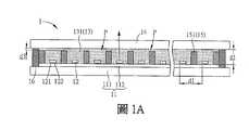
圖1A為本發明較佳實施例之一種顯示裝置的示意圖。FIG. 1A is a schematic diagram of a display device according to a preferred embodiment of the present invention.
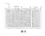
圖1B為對應於圖1A的上視示意圖。Fig. 1B is a schematic top view corresponding to Fig. 1A.
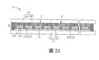
圖2A與圖3A分別為本發明不同實施態樣的顯示裝置的示意圖。2A and 3A are schematic diagrams of display devices in different embodiments of the present invention.
圖2B與圖3B分別為對應於圖2A與圖3A的上視示意圖。2B and 3B are schematic top views corresponding to FIGS. 2A and 3A, respectively.
圖3C與圖4A分別為本發明不同實施態樣的顯示裝置的示意圖。3C and 4A are respectively schematic diagrams of display devices in different embodiments of the present invention.
圖3D與圖4B分別為對應於圖3C與圖4A的上視示意圖。3D and 4B are schematic top views corresponding to FIGS. 3C and 4A, respectively.
圖5A、圖6A與圖7分別為本發明不同實施態樣的顯示裝置的示意圖。5A, 6A and 7 are schematic diagrams of display devices in different embodiments of the present invention.
圖5B與圖6B分別為對應於圖5A與圖5B的上視示意圖。5B and 6B are schematic top views corresponding to FIGS. 5A and 5B, respectively.
以下將參照相關圖式,說明依本發明較佳實施例之顯示裝置,其中相同的元件將以相同的參照符號加以說明。Hereinafter, the display device according to the preferred embodiment of the present invention will be described with reference to related drawings, in which the same elements will be described with the same reference signs.
為了說明顯示裝置的結構,以下實施例中出現的上視示意圖中只顯示必要的元件及其相對關係,並未顯示出剖視示意圖中的所有元件。In order to illustrate the structure of the display device, the top schematic diagrams appearing in the following embodiments only show necessary components and their relative relationships, and do not show all components in the cross-sectional schematic diagram.
圖1A為本發明較佳實施例之一種顯示裝置1的示意圖,圖1B為對應於圖1A的上視示意圖。如圖1A與圖1B所示,本實施例的顯示裝置1為一種平面顯示裝置,並具有多數個畫素,各畫素具有複數次畫素P。顯示裝置1可包括一電路基板11、多數個微發光半導體元件12、一光轉換層13以及一對向基板14。另外,本實施例的顯示裝置1更可包括一黑色矩陣層15及一密封層16。FIG. 1A is a schematic diagram of a
電路基板11可為一主動矩陣(Active Matrix,AM)電路基板或被動矩陣(Passive Matrix,PM)電路基板,而該些微發光半導體元件12間隔設置於電路基板11的表面上。本實施例的電路基板11是以主動矩陣式電路基板為例。主動矩陣式電路基板(電路基板11)可包含一基材111與一矩陣電路112,矩陣電路112設置於基材111面向對向基板14的表面上,且該些微發光半導體元件12設置於矩陣電路112上,並分別與矩陣電路112電性連接。The
在實施上,基材111可為軟性基材或為硬性基材,並為可透光或不可透光材料製成。其中,透光材料例如是玻璃、石英、藍寶石或類似物、塑膠、橡膠、玻璃纖維或其他高分子材料,較佳的可為硼酸鹽無鹼玻璃基板(alumino silicate glass substrate)或為有機高分子材料。在一些實施例中,上述的有機高分子材料例如但不限於為聚亞醯胺(Polyimide,PI)、聚碳酸酯(Polycarbonate,PC)或聚乙烯對苯二甲酸酯(Polyethylene Terephthalate,PET)。若是聚亞醯胺(PI)的話,其玻璃轉換溫度可例如介於攝氏400度至攝氏600度之間。In practice, the
本實施例的電路基板11可例如為液晶顯示面板中的主動式矩陣電路基板。電路基板11的矩陣電路112可包含佈設有交錯的資料線與掃描線、多個主動元件(如薄膜電晶體)、掃描驅動電路、資料驅動電路及時序控制電路…等元件。其中,一個次畫素P可對應一個主動元件與至少一個微發光半導體元件12,且各主動元件與至少一個微發光半導體元件12電性連接。藉由掃描線控制主動元件,可使資料線所傳送的資料電壓通過開關元件傳送至微發光半導體元件12,使微發光半導體元件12發光。由於主動式矩陣電路基板為液晶顯示裝置的習知技藝,也不是本發明的重點,本領域技術人員當可找到相關技術內容,在此不再進一步作說明。The
該些微發光半導體元件12可陣列排列而配置於電路基板11的矩陣電路112上。在一些實施例中,微發光半導體元件12可例如以表面貼裝技術(SMT)而與矩陣電路112電性連接。本實施例的微發光半導體元件12是以微發光二極體(μLED)為例,使顯示裝置1為一μLED顯示裝置。本實施例的該些微發光半導體元件12為二維陣列排列,然並不以此為限,在不同的實施例中,該些微發光半導體元件12也可為一維陣列排列。The micro light-emitting
該些微發光半導體元件12分別與該些次畫素P對應設置。本實施例的一個微發光半導體元件12可分別對應一個次畫素P,不過,並不以此為限,在不同的實施例中,也可多個微發光半導體元件12對應一個次畫素P。微發光半導體元件12的邊長可分別大於等於1微米(μm),且小於等於100μm。在一些實施例中,微發光半導體元件12的邊長可例如小於50μm,例如為25μm×25μm。另外,相鄰兩個微發光半導體元件12的最小間距d1例如但不限於為1微米,藉此,可以製作解析度相當高的顯示器,例如醫療用的顯示器。The micro light emitting
微發光半導體元件12(微發光二極體)可為雙電極元件或三電極元件。本實施例是以雙電極元件為例。其中,微發光半導體元件12的兩個電極121、122可為p極與n極在同一側(水平結構),或p極與n極分別在上下兩側(上下導通型或垂直結構)。本實施例是以水平結構的μLED為例。此外,若以顯色波長來分類,微發光半導體元件12可為藍光發光二極體,或者為紅光、綠光、紅外光、紫外光(UV光)等微發光二極體,或其組合。或者,在不同實施例中,微發光半導體元件12也可同時發出藍光與綠光,並不限制。因此,在本實施例的顯示裝置1中,可依據顯示畫面的局部發光需求,透過電路基板11之矩陣電路112的驅動,使對應於各次畫素P的各微發光半導體元件12(μLED)分別被點亮而發光(不需發光的微發光半導體元件12可不需點亮),藉此可使顯示裝置1達到局部調光(local dimming)的功效,進而能夠節省電能。The micro light emitting semiconductor element 12 (micro light emitting diode) may be a two-electrode element or a three-electrode element. In this embodiment, a two-electrode element is taken as an example. Among them, the micro light emitting
光轉換層13設置於該些微發光半導體元件12上。光轉換層13的厚度d2可大於或等於6微米,且小於或等於30微米。另外,光轉換層13具有多數個光轉換部131,該些光轉換部131分別與至少部份的該些微發光半導體元件12對應設置。本實施例的該些光轉換部131分別與該些微發光半導體元件12對應設置。光轉換部131可具有光致發光材料,當光線進入光轉換部131後,可激發光轉換部131發出不同顏色的光線。具體來說,本實施例的微發光半導體元件12所發出的光線進入光轉換部131後會激發出不同顏色的光線,並由光轉換部131射出白光。The
光轉換層13的光轉換部131可具有至少一光轉換物質,光轉換物質可為量子點(Quantum dots)或螢光顆粒。本實施例的光轉換部131的光轉換物質是以量子點為例,且較佳具有二種形狀或尺寸不相同的量子點,以吸收由微發光半導體元件12所發出的高能光線而激發出不同頻段的可見光,例如二種量子點可吸收高能的藍光或UV光而激發出低能量的紅光與綠光,未吸收完的殘餘高能藍光與被二種量子點激發出的紅光與綠光由光轉換部131射出而形成白光;或者,在不同實施例中,光轉換部131的量子點可吸收由微發光半導體元件12所發出的高能的藍光與綠光而激發出低能量的紅光(此態樣只有一種尺寸或形狀的量子點,光轉換部131的轉換效率較好),未吸收完的殘餘高能藍光、綠光與被激發出的紅光由光轉換部131射出而形成白光。The
特別說明的是,在實施上,上述的光轉換物質(量子點或螢光顆粒)可均勻混合於一膠材(例如環氧樹脂)中而形成如“果凍狀”的光轉換材料,再將此材料塗佈並覆蓋在該些微發光半導體元件12與矩陣電路112上,經固化後形成光轉換層13。另外,藉由黑色矩陣層15的各遮光區段151圍繞各微發光半導體元件12而設置,以形成該些光轉換部131,進而可得到對應於多個光轉換部131與多個微發光半導體元件12的多個次畫素P(於此係以一個次畫素對應一微發光半導體元件為例,當然一個次畫素中也可以且有多個微發光半導體元件)。值得一提的是,本實施例的黑色矩陣層15的各遮光區段151雖圍繞著各微發光半導體元件12而設置,但與對向基板14之間有一間距d3。不過,在不同的實施例中,黑色矩陣層15的各遮光區段151也可頂抵到對向基板14,本發明不限制。In particular, in practice, the above-mentioned light conversion material (quantum dots or fluorescent particles) can be uniformly mixed in a glue material (such as epoxy resin) to form a "jelly-like" light conversion material, and then This material is coated and covered on the micro light emitting
另外,習知的作法不會讓光線在光轉換層形成白光而射出(習知不會使各次畫素P對應的光線顏色皆為相同的白光),而是使一個次畫素P對應一種顏色的光線(相鄰次畫素的顏色不相同)。因此,在習知的作法中,光轉換層要先製作出RGB圖案(RGB pattern),也就是說為了發出不同顏色的RGB圖案,必須分別具有不同種類的光轉換物質,且要分別形成於微發光半導體元件12之上,並不需彩色濾光層(Color Filter)就可製成全彩顯示器,故於製程上較為繁複也提高了製程成本。但是,在本實施例的顯示裝置1中,光轉換層13並不需要對應於各發光元件而製作出一個一個的RGB圖案的光轉換部,而是將光轉換物質均勻混合於膠材後直接塗佈且覆蓋在微發光半導體元件12上而形成一層光轉換層13,且以遮光區段151隔開以分別形成對應於各微發光半導體元件12的光轉換部(故各光轉換部的成分配方一樣),因此,不僅材料製備容易,製程也較簡單,使得顯示裝置1的結構簡單,而且製作成本也較低。In addition, the conventional method does not allow light to form white light on the light conversion layer and emits it (the conventional art does not make the light color corresponding to each sub-pixel P be the same white light), but makes one sub-pixel P correspond to one type Color light (the colors of adjacent sub-pixels are not the same). Therefore, in the conventional method, the light conversion layer must first be made into an RGB pattern (RGB pattern), that is to say, in order to emit different colors of RGB patterns, different types of light conversion materials must be provided, and they must be formed in the micro On the light-emitting
對向基板14設置於光轉換層13遠離電路基板11的一側。本實施例的光轉換層13是夾置於對向基板14與電路基板11之間,並且,是藉由設置於電路基板11上的黑色矩陣層15將單一層的光轉換層13分隔成複數個光轉換部131(兩個光轉換部131之間有連接或不連接皆可)。於此,黑色矩陣層15的遮光區段151與次畫素P之光轉換部131及微發光半導體元件12對應設置,使一個次畫素P對應一個光轉換部131與一個微發光半導體元件12。其中,黑色矩陣層15的作用為避免相鄰次畫素混光,其材料可與習知液晶顯示裝置中的黑色矩陣(BM)相同,於此不再多做說明。The
對向基板14可為軟性基板或硬性基板,並可為一保護基材、一單色濾光基板(例如藍色濾光基板)或一彩色濾光基板。其中,保護基材可為保護蓋板、保護層或保護膜層,並不限制。本實施例的對向基板14是以可透光的保護基材為例,例如為玻璃或高分子透光基材。另外,當對向基板14為保護基材或單色濾光基板時,可例如藉由控制各次畫素P對應的各微發光半導體元件12的發光強度來得到單色顯示器的效果,使顯示裝置1為單色顯示器(monochrome display);此外,當對向基板14為彩色濾光基板時,例如包含R、G、B三種顏色或R、G、B、W四種顏色的濾光材料時,則可使顯示裝置1成為全彩顯示器,以下會再說明。The
密封層16設置於電路基板11與對向基板14的外周圍。在一些實施例中,密封層16可為光固化膠(例如UV膠),並例如但不限於大氣中以塗佈方式環設於電路基板11與對向基板14的外周圍,使光轉換層13位於密封層16、電路基板11與對向基板14之間。在另一些實施例中,密封層16也可為熱固化膠,或者是光固化膠與熱固化膠的組合,並不限制。The
圖2A為本發明另一實施態樣的顯示裝置1a的示意圖,圖2B為對應於圖2A的上視示意圖。如圖2A與圖2B所示,與圖1A與圖1B的顯示裝置1主要的不同在於,本實施態樣的顯示裝置1a的對向基板14不是保護基材,而是一彩色濾光基板。其中,彩色濾光基板(對向基板14)可包含一透光基材141及多數個濾光部142,其中,各濾光部142對應一個次畫素P,並設置於各光轉換部131與透光基材141之間,且分別與各微發光半導體元件12對應設置。2A is a schematic diagram of a display device 1a according to another embodiment of the present invention, and FIG. 2B is a schematic top view corresponding to FIG. 2A. As shown in FIGS. 2A and 2B, the main difference from the
透光基材141可為硬板或軟板,並不限制。本實施例的該些濾光部142包含依序設置的紅色(R)、綠色(G)與藍色(B)濾光部,以讓對應的紅色、綠色與藍色三原色光通過。在不同實施態樣中,該些濾光部142也可包含依序設置的紅色(R)、綠色(G)、藍色(B)與白色(W)濾光部;或者,若該些濾光部142的顏色皆相同的話,則可使顯示裝置成為單色顯示器。上述的彩色濾光基板可為習知液晶顯示裝置中的彩色濾光基板(color filter substrate,CF substrate),藉此協助顯示裝置1a全彩化。此外,本實施例的黑色矩陣層15的各遮光區段151與對向基板14上的該些濾光部142之間一樣有間隙。在不同的實施例中,黑色矩陣層15的各遮光區段151也可分別延伸且接觸透光基材141,使兩個濾光部142之間有一個遮光區段151,並不限制。The light-transmitting
此外,顯示裝置1a的其他技術特徵可參照顯示裝置1的相同元件,不再贅述。In addition, other technical features of the display device 1a can be referred to the same elements of the
圖3A為本發明又一實施態樣的顯示裝置1b的示意圖,圖3B為對應於圖3A的上視示意圖。如圖3A與圖3B所示,與圖2A與圖2B的顯示裝置1a主要的不同在於,顯示裝置1b更可包括一透明光阻件17,透明光阻件17例如與液晶顯示面板之間隔物(Photo-Sacer)的材料相同,可使用例如樹脂類、矽酸鹽類、或玻璃纖維類等感光性透明光阻件材料來製作。透明光阻件17可設置於對向基板14的透光基材141上,並覆蓋該些微發光半導體元件12的至少其中之一,且該些微發光半導體元件12的至少其中之一可發出藍光或綠光。在本實施態樣中,濾光部142只包含依序設置的紅色濾光部與綠色濾光部,並不包含藍色濾光部,其原因是:因為本實施態樣的該些微發光半導體元件12是發出藍光,因此,只要使微發光半導體元件12所發出的藍光直接由透光基材141射出即可,不需要設置光轉換部131與對應的藍色濾光材料。換言之,透明光阻件17設置於透光基材141上,並可覆蓋發出藍光的微發光半導體元件12上,且對向基板14對應透明光阻件17之處不需設置藍色濾光部的濾光材料(與光轉換部131),使微發光半導體元件12所發出的藍光直接穿過透明光阻件17與透光基材141射出即可,同樣可使顯示裝置1b為全彩顯示器。藉此,可以節省藍色濾光部與對應的光轉換部131的材料成本。FIG. 3A is a schematic diagram of a
另外,在實務上,可將透明光阻件17對應設置在透光基材141原先設置藍色濾光部之處,且將具有透明光阻件17的透光基材141反置而插入可發出藍光的微發光半導體元件12所對應的光轉換部的位置,以擠掉該位置的光轉換材料。由於在圖2A與圖2B中,微發光半導體元件12發出的藍光在光轉換部131中會被光轉換物質吸收一部分的能量,但是,本實施態樣因為沒有設置光轉換部與藍色濾光材料,因此輸入微發光半導體元件12的電流值可以比較小(小於紅色濾光部與綠色濾光部所對應的微發光半導體元件12的電流值),亮度可以比較低。因此,藉由透明光阻件17的設置,不僅可以節省輸入微發光半導體元件12的電流值而減少功耗,也可保持對向基板14與電路基板11之間的間隙。In addition, in practice, the
此外,顯示裝置1b的其他技術特徵可參照顯示裝置1a的相同元件,不再贅述。In addition, other technical features of the
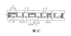
另外,圖3C為本發明不同實施態樣的顯示裝置的示意圖,而圖3D為對應於圖3C的上視示意圖。如圖3C與圖3D所示,與圖3A與圖3B的顯示裝置1b主要的不同於,在本實施態樣中,對應於紅色濾光部142的微發光半導體元件12可發出藍光,或者發出UV光,或者同時發出藍光與綠光,但對應於原綠色濾光部位置的微發光半導體元件12是發出綠光,且對應於原藍色濾光部的位置的微發光半導體元件12是發出藍光。因此,透明光阻件17除了設置於原藍色濾光部的位置之外,更設置於原綠色濾光部的位置,使得微發光半導體元件12所發出的綠光與藍光可分別通過透明光阻件17後直接由透光基材141射出(不需通過光轉換部131,也不需通過綠色濾光部與藍色濾光部),因此,同樣可使顯示裝置成為全彩顯示器。藉此,不僅可節省藍色濾光部與綠色濾光部與對應的光轉換部131的材料成本外,也由於沒有設置光轉換部、藍色與綠色濾光材料,因此輸入該些微發光半導體元件12的總電流值可以更小,更可節省輸入微發光半導體元件12的電流值而可減少更多的功耗。此外,如圖3C所示,本實施態樣中的兩個透明光阻件17之間的遮光區段151將透明光阻件17完全隔開,避免相鄰兩次畫素P的綠光與藍光混光。In addition, FIG. 3C is a schematic diagram of a display device according to different embodiments of the present invention, and FIG. 3D is a schematic top view corresponding to FIG. 3C. As shown in FIGS. 3C and 3D, the main difference from the
於上述實施例中,微發光半導體元件所發出之光線經過光轉換層後產生白光的設計概念也可應用於平面顯示裝置的背光模組中。In the above-mentioned embodiments, the design concept that the light emitted by the micro-luminescence semiconductor device generates white light after passing through the light conversion layer can also be applied to the backlight module of the flat display device.
圖4A為本發明不同實施例之顯示裝置2的示意圖,圖4B為對應於圖4A的上視示意圖。於此,圖4B只顯示背光模組21的上視示意圖中的必要元件,未顯示其他元件。4A is a schematic diagram of a
如圖4A與圖4B所示,本實施例的顯示裝置2為平面顯示裝置,例如但不限於為液晶顯示裝置。顯示裝置1可包括一背光模組21以及一顯示面板22,背光模組21與顯示面板22相對設置,並可發出光線穿過顯示面板22,使顯示面板22顯示影像。本實施例之顯示面板22為液晶顯示面板,例如但不限於為平面切換(in-plane switch,IPS)式液晶顯示面板、邊緣電場切換(fringe field switching,FFS)式液晶顯示面板或垂直配向模態(vertical alignment mode,VA mode)液晶顯示面板,並不限制。As shown in FIGS. 4A and 4B, the
背光模組21為一直下式背光模組,並包含一電路基板211、多數個微發光半導體元件212及一光轉換層213。本實施例的微發光半導體元件212仍以微發光二極體(μLED)為例。該些微發光半導體元件212間隔設置於電路基板211上。其中,電路基板211可為一軟性電路基板或一硬性電路基板。本實施例的電路基板211例如為軟性電路基板,並可包含一軟性基材2111及驅動該些微發光半導體元件212的一驅動電路2112,藉此,可利用電路基板211的驅動電路2112控制該些微發光半導體元件212發光。具體來說,可依據顯示面板22之顯示畫面需求,透過電路基板211的驅動,使對應的微發光半導體元件212分別被點亮而發光(或使部份微發光半導體元件212不發光),藉此,使顯示裝置2之背光模組21可達到局部調光的功效。The
在實施上,軟性基材2111可為透光或不可透光材料製成。透光材料例如可為有機高分子材料。在一些實施例中,有機高分子材料例如但不限於為聚亞醯胺(PI)、聚碳酸酯(PC)或聚乙烯對苯二甲酸酯(PET)。若是聚亞醯胺(PI)的話,其玻璃轉換溫度可例如介於攝氏400度至攝氏600度之間。In practice, the
光轉換層213設置於該些微發光半導體元件212上。其中,該些微發光半導體元件212所發出之光線經過光轉換層213後產生白光。在一些實施例中,光轉換層213可具有至少一光轉換物質,而光轉換物質可為量子點或螢光顆粒。在實施上,量子點或螢光顆粒可混合於膠材中而形成光轉換材料,光轉換材料可塗佈並覆蓋該些微發光半導體元件212與驅動電路2112上經固化後形成光轉換層213(本實施例沒有設置上述顯示裝置1的黑色矩陣層15)。The
本實施例的光轉換層213的光轉換物質是以量子點為例,其可吸收由微發光半導體元件212所發出的高能光線,例如可吸收高能的藍光或UV光而激發出低能量的紅光與綠光,未吸收完的殘餘高能藍光與被激發出的紅光與綠光由光轉換層213射出而形成白光;或者,在不同實施例中,光轉換層213的量子點可吸收由微發光半導體元件212同時發出的高能藍光與綠光而激發出低能量的紅光,未吸收完的殘餘高能藍光、綠光與被激發出的紅光由光轉換層213射出而形成白光。The light conversion material of the
本實施例的背光模組21更可包含一對向基板214,對向基板214可為硬板或軟板,並設置於光轉換層213與顯示面板22之間。另外,本實施例的背光模組21更可包含一密封層24,密封層24設置於電路基板211與對向基板214的外周圍。在一些實施例中,密封層24可為光固化膠(例如UV膠),並例如但不限於大氣中以塗佈方式環設於電路基板211與對向基板214的外周圍,使光轉換層213位於密封層24、電路基板211與對向基板214之間。在另一些實施例中,密封層24也可為熱固化膠,或者是光固化膠與熱固化膠的組合,並不限制。The
此外,本實施例的背光模組21更可包含至少一光學膜片23,光學膜片23設置於顯示面板22與對向基板214之間。在一些實施例中,光學膜片23的數量可為複數,並例如但不限於為擴散板、90°集光片、0°集光片或增亮片,或其組合,藉此,使由光轉換層213射出且經由對向基板214的光線再穿過光學膜片23後可形成更為均勻的面光源,以提供給顯示面板22使用。In addition, the
值得說明的是,在不同的實施例中,也可不需在顯示面板22與對向基板214之間設置光學膜片23,藉此可節省光學膜片23的材料成本;或者,也可不需設置對向基板214,利用光學膜片23取代對向基板214的作用,使顯示面板22與光轉換層213之間只存在著光學膜片23,以節省對向基板214的材料成本;或者,設置有對向基板214,但此對向基板214本身就是光學膜材,以節省成本,本發明皆不限制。It is worth noting that in different embodiments, the
另外,圖5A、圖6A與圖7分別為本發明不同實施態樣的顯示裝置2a~2c的示意圖,圖5B與圖6B分別為對應於圖5A與圖5B的上視示意圖。於此,圖5B與圖6B仍只顯示背光模組21a、21b的上視示意圖。In addition, FIG. 5A, FIG. 6A and FIG. 7 are respectively different embodiments of the present invention.The schematic diagrams of the
如圖5A與圖5B所示,與圖4A與圖4B的顯示裝置2主要的不同在於,本實施例的顯示裝置2a更可包括一黑色矩陣層25,黑色矩陣層25設置電路基板211上,並圍繞該些微發光半導體元件212而設置。其中,黑色矩陣層25的一個遮光區段251圍繞一個微發光半導體元件212,避免混光。各遮光區段251雖圍繞著各微發光半導體元件212而設置,但與對向基板214之間仍有一間距。在不同實施例中,各遮光區段251與對向基板214也可連接而沒有間距。As shown in FIG. 5A and FIG. 5B, the main difference from the
另外,如圖6A與圖6B所示,與圖5A與圖5B的顯示裝置2a主要的不同在於,在本實施例的黑色矩陣層25中,並不是一個遮光區段251圍繞一個微發光半導體元件212而設置,而是一個遮光區段251圍繞多個微發光半導體元件212而設置。在實施上,遮光區段251所圍繞的微發光半導體元件212的區域可例如但不限於為2×2、2×3或3×4、…個微發光半導體元件212,視設計需求而定。換言之,不一定要每一顆微發光半導體元件212的周圍就設置一個遮光區段251,可以是一區塊內的多個微發光半導體元件212的周圍設置一個遮光區段251即可,依設計者的需求任意調配,這樣設計的好處是,可依需求控制一整個區塊的微發光半導體元件212發光或不發光,以達到局部調光的效果,藉此,可使驅動微發光半導體元件212的驅動電路2112較簡單,成本也較低。In addition, as shown in FIGS. 6A and 6B, the main difference from the
另外,如圖7所示,與圖4A的顯示裝置2主要的不同在於,本實施態樣的顯示裝置2c的背光模組21c並沒有設置對向基板214,且光轉換層213為一光學膜材,例如但不限於為量子點膜(QD Film)。在實施上,由於光轉換層213為一光學膜材,因此可依需求尺寸大小直接由大尺寸的光學膜材中裁切所需大小,並貼附於微發光半導體元件212上,因此,不僅光轉換層213的材料製備容易,製程也較簡單,使得顯示裝置2c的結構簡單,而且製作成本也較低。另外,本實施例的顯示裝置2c並不設置密封層24,不過,在不同實施例中,也可與顯示裝置2相同而設置密封層24在電路基板211與對向基板214的外周圍。In addition, as shown in FIG. 7, the main difference from the
此外,顯示裝置2a~2c的其他技術特徵可參照顯示裝置2的相同元件,於此不再贅述。In addition, other technical features of the
綜上所述,在本發明之顯示裝置中,藉由光轉換層設置於該些微發光半導體元件上,並具有多數個光轉換部,該些光轉換部分別與至少部份的該些微發光半導體元件對應設置,且各次畫素對應的微發光半導體元件所發出之光線經過光轉換部後產生白光的結構設計;或者,藉由顯示面板與背光模組相對設置,且背光模組的光轉換層設置於該些微發光半導體元件上,該些微發光半導體元件所發出之光線經過該光轉換層後產生白光的結構設計,不僅使本發明的顯示裝置有別於習知技術的平面顯示裝置而具有結構簡單的優點之外,更可達到省電與局部調光的功效。此外,在本發明一些實施例中,不僅材料製備容易,製程也較簡單,使得本發明的顯示裝置的結構較簡單,而且製作成本也較低。To sum up, in the display device of the present invention, the light conversion layer is disposed on the micro light emitting semiconductor elements, and there are a plurality of light conversion parts, and the light conversion parts are connected with at least part of the micro light emitting semiconductor elements. The elements are correspondingly arranged, and the light emitted by the micro-luminescence semiconductor element corresponding to each pixel passes through the light conversion part to generate white light; or, the display panel and the backlight module are arranged oppositely, and the light conversion of the backlight module The layer is arranged on the micro-light-emitting semiconductor elements, and the light emitted by the micro-light-emitting semiconductor elements passes through the light conversion layer to generate white light. The structure design not only distinguishes the display device of the present invention from the flat display device of the prior art, In addition to the advantages of simple structure, power saving and local dimming can be achieved. In addition, in some embodiments of the present invention, not only the material preparation is easy, but the manufacturing process is also simple, so that the structure of the display device of the present invention is simpler, and the manufacturing cost is also lower.
以上所述僅為舉例性,而非為限制性者。任何未脫離本發明之精神與範疇,而對其進行之等效修改或變更,均應包含於後附之申請專利範圍中。The above descriptions are merely illustrative and not restrictive. Any equivalent modifications or alterations that do not depart from the spirit and scope of the present invention should be included in the scope of the appended patent application.
1:顯示裝置1: display device
11:電路基板11: Circuit board
111:基材111: Substrate
112:矩陣電路112: Matrix Circuit
12:微發光半導體元件12: Micro-luminescent semiconductor components
121、122:電極121, 122: Electrode
13:光轉換層13: Light conversion layer
131:光轉換部131: Light Conversion Department
14:對向基板14: Opposite substrate
15:黑色矩陣層15: Black matrix layer
151:遮光區段151: Shading section
16:密封層16: Sealing layer
d1:最小間距d1: minimum spacing
d2:厚度d2: thickness
d3:間距d3: spacing
P:次畫素P: Sub-pixel
Claims (15)
Translated fromChinesePriority Applications (5)
| Application Number | Priority Date | Filing Date | Title |
|---|---|---|---|
| TW106135764ATWI739931B (en) | 2017-10-18 | 2017-10-18 | Display device |
| CN201811053980.6ACN109683390A (en) | 2017-10-18 | 2018-09-11 | Display device |
| CN202311362565.XACN117608121A (en) | 2017-10-18 | 2018-09-11 | display device |
| CN202311362566.4ACN117608122A (en) | 2017-10-18 | 2018-09-11 | display device |
| US16/162,752US10672347B2 (en) | 2017-10-18 | 2018-10-17 | Display device |
Applications Claiming Priority (1)
| Application Number | Priority Date | Filing Date | Title |
|---|---|---|---|
| TW106135764ATWI739931B (en) | 2017-10-18 | 2017-10-18 | Display device |
Publications (2)
| Publication Number | Publication Date |
|---|---|
| TW201917922A TW201917922A (en) | 2019-05-01 |
| TWI739931Btrue TWI739931B (en) | 2021-09-21 |
Family
ID=66097090
Family Applications (1)
| Application Number | Title | Priority Date | Filing Date |
|---|---|---|---|
| TW106135764ATWI739931B (en) | 2017-10-18 | 2017-10-18 | Display device |
Country Status (3)
| Country | Link |
|---|---|
| US (1) | US10672347B2 (en) |
| CN (3) | CN109683390A (en) |
| TW (1) | TWI739931B (en) |
Families Citing this family (19)
| Publication number | Priority date | Publication date | Assignee | Title |
|---|---|---|---|---|
| CN108573992A (en)* | 2018-05-08 | 2018-09-25 | 业成科技(成都)有限公司 | Display panel, manufacturing method and electronic device using the display panel |
| JP6963720B2 (en)* | 2018-08-30 | 2021-11-10 | 日亜化学工業株式会社 | Light emitting device |
| CN110875345A (en)* | 2018-08-31 | 2020-03-10 | 昆山工研院新型平板显示技术中心有限公司 | LED display device and manufacturing method thereof, and LED display panel |
| JP7321832B2 (en)* | 2019-08-23 | 2023-08-07 | 株式会社ジャパンディスプレイ | Lighting device and display device |
| CN111261656A (en)* | 2020-01-17 | 2020-06-09 | 深圳市华星光电半导体显示技术有限公司 | A display panel and its manufacturing method |
| CN112965287B (en)* | 2020-05-08 | 2022-11-29 | 重庆康佳光电技术研究院有限公司 | Preparation method of color film substrate, display device and display back plate |
| TWI766293B (en)* | 2020-06-09 | 2022-06-01 | 友達光電股份有限公司 | Display panel |
| KR102827123B1 (en)* | 2020-06-19 | 2025-07-01 | 삼성전자주식회사 | Backlight unit having micro emitting device and liquid crystal display |
| CN114005911B (en)* | 2020-07-27 | 2023-12-26 | Tcl科技集团股份有限公司 | Display device and preparation method thereof |
| CN112310143A (en)* | 2020-11-02 | 2021-02-02 | 广东省科学院半导体研究所 | Quantum dot micro-LED display device and preparation method thereof |
| WO2022097339A1 (en)* | 2020-11-04 | 2022-05-12 | 株式会社ジャパンディスプレイ | Display device |
| JP2023549801A (en)* | 2020-11-11 | 2023-11-29 | アプライド マテリアルズ インコーポレイテッド | display front panel device |
| TWI747690B (en)* | 2020-12-28 | 2021-11-21 | 友達光電股份有限公司 | Display device and manufacturing method thereof |
| JP7635056B2 (en)* | 2021-04-02 | 2025-02-25 | 株式会社ジャパンディスプレイ | Electronic component mounting method, display device, and circuit board |
| CN114038984B (en)* | 2021-12-02 | 2023-03-31 | 业成科技(成都)有限公司 | Micro light emitting diode display and forming method thereof |
| TWI815261B (en) | 2021-12-27 | 2023-09-11 | 財團法人工業技術研究院 | Light color conversion layer structure, method of manufacturing the same and light emitting device containing the same |
| WO2023123263A1 (en)* | 2021-12-30 | 2023-07-06 | 厦门市芯颖显示科技有限公司 | Display panel and manufacturing method therefor |
| WO2025065332A1 (en)* | 2023-09-27 | 2025-04-03 | 京东方科技集团股份有限公司 | Light-emitting substrate, backlight source, and display apparatus |
| CN117525249A (en)* | 2024-01-04 | 2024-02-06 | 南京国兆光电科技有限公司 | Single red micro display structure |
Citations (3)
| Publication number | Priority date | Publication date | Assignee | Title |
|---|---|---|---|---|
| TW201515260A (en)* | 2013-06-18 | 2015-04-16 | 樂福科技股份有限公司 | LED display with wavelength conversion layer |
| US20150300576A1 (en)* | 2014-04-21 | 2015-10-22 | Canon Kabushiki Kaisha | Light source apparatus and image display apparatus |
| CN107068707A (en)* | 2017-06-13 | 2017-08-18 | 深圳市华星光电技术有限公司 | Micro LED chromatic displays |
Family Cites Families (15)
| Publication number | Priority date | Publication date | Assignee | Title |
|---|---|---|---|---|
| US20120250350A1 (en)* | 2011-03-30 | 2012-10-04 | Mangeun Kim | Display apparatus |
| US9484504B2 (en)* | 2013-05-14 | 2016-11-01 | Apple Inc. | Micro LED with wavelength conversion layer |
| TWI574055B (en)* | 2013-08-14 | 2017-03-11 | 鴻海精密工業股份有限公司 | Display panel |
| US9541794B2 (en)* | 2014-01-10 | 2017-01-10 | Apple Inc. | High dynamic range liquid crystal display |
| WO2015152116A1 (en)* | 2014-03-31 | 2015-10-08 | 富士フイルム株式会社 | Optical conversion member, method for manufacturing optical conversion member, and backlight unit and liquid crystal display device including optical conversion member |
| US10304813B2 (en)* | 2015-11-05 | 2019-05-28 | Innolux Corporation | Display device having a plurality of bank structures |
| JP2017091866A (en)* | 2015-11-12 | 2017-05-25 | キヤノン株式会社 | Light emitting device |
| TWI588984B (en)* | 2016-03-14 | 2017-06-21 | 群創光電股份有限公司 | Display device |
| KR102687577B1 (en)* | 2016-12-30 | 2024-07-22 | 엘지디스플레이 주식회사 | Light emitting diode display apparatus and multi screen display apparatus using the same |
| JP2018198187A (en)* | 2017-05-25 | 2018-12-13 | キヤノン株式会社 | Light emitting device and display device |
| CN107230685A (en)* | 2017-06-02 | 2017-10-03 | 南京迈智芯微光电科技有限公司 | The semiconductor light emitting micro-display and its manufacturing process of a kind of true color |
| US10514574B2 (en)* | 2017-07-24 | 2019-12-24 | Wuhan China Star Optoelectronics Technology Co., Ltd | Direct type backlight module and liquid crystal display |
| US20190041701A1 (en)* | 2017-08-01 | 2019-02-07 | Innolux Corporation | Display device |
| KR102476136B1 (en)* | 2017-09-05 | 2022-12-09 | 삼성전자주식회사 | Display device using light emitting diode |
| TWI628477B (en)* | 2017-09-27 | 2018-07-01 | 睿亞光電股份有限公司 | Backlight device |
- 2017
- 2017-10-18TWTW106135764Apatent/TWI739931B/enactive
- 2018
- 2018-09-11CNCN201811053980.6Apatent/CN109683390A/enactivePending
- 2018-09-11CNCN202311362565.XApatent/CN117608121A/enactivePending
- 2018-09-11CNCN202311362566.4Apatent/CN117608122A/enactivePending
- 2018-10-17USUS16/162,752patent/US10672347B2/enactiveActive
Patent Citations (3)
| Publication number | Priority date | Publication date | Assignee | Title |
|---|---|---|---|---|
| TW201515260A (en)* | 2013-06-18 | 2015-04-16 | 樂福科技股份有限公司 | LED display with wavelength conversion layer |
| US20150300576A1 (en)* | 2014-04-21 | 2015-10-22 | Canon Kabushiki Kaisha | Light source apparatus and image display apparatus |
| CN107068707A (en)* | 2017-06-13 | 2017-08-18 | 深圳市华星光电技术有限公司 | Micro LED chromatic displays |
Also Published As
| Publication number | Publication date |
|---|---|
| US10672347B2 (en) | 2020-06-02 |
| CN117608121A (en) | 2024-02-27 |
| CN109683390A (en) | 2019-04-26 |
| US20190114974A1 (en) | 2019-04-18 |
| TW201917922A (en) | 2019-05-01 |
| CN117608122A (en) | 2024-02-27 |
Similar Documents
| Publication | Publication Date | Title |
|---|---|---|
| TWI739931B (en) | Display device | |
| KR102527428B1 (en) | Display device | |
| TWI569071B (en) | Optical member and display device having the same | |
| CN105425501B (en) | Optical element and the display device using the optical element, electronic equipment, lighting device | |
| CN103531100B (en) | Display device and operating method thereof | |
| JP2016070949A (en) | Display device | |
| CN101122716A (en) | Backlight assembly and display device with the backlight assembly | |
| KR101236515B1 (en) | Color filter substrate for liquid crystal display and method for fabricating the same | |
| CN105607346A (en) | Graphene backlight module and liquid crystal display device | |
| JP2016133730A (en) | Display device | |
| US7545466B2 (en) | Liquid crystal display device and substrate therefor | |
| US20100134483A1 (en) | Driving method thereof | |
| CN106033163B (en) | Display panel | |
| CN101893780A (en) | color filter | |
| CN100403125C (en) | Backlight unit of liquid crystal display device using light emitting diode and driving method thereof | |
| CN102053407A (en) | Liquid crystal display device having a plurality of pixel electrodes | |
| KR20110022970A (en) | Display | |
| KR20190143243A (en) | LED Module and backlight Module having the same and Display Device having the same | |
| WO2012098975A1 (en) | Display panel and display device with same | |
| CN106154619B (en) | display panel | |
| CN104101940B (en) | Light guide plate, backlight and display device | |
| CN114049849B (en) | Display screen | |
| CN104280925A (en) | Display panel and display device | |
| KR100791027B1 (en) | Display panel | |
| KR102102703B1 (en) | LED package, method of fabricating the same, and backlight unit and liquid crystal display device including the LED package |