TWI738842B - Component inspection circuit, component inspection device and probe card - Google Patents
Component inspection circuit, component inspection device and probe cardDownload PDFInfo
- Publication number
- TWI738842B TWI738842BTW106127068ATW106127068ATWI738842BTW I738842 BTWI738842 BTW I738842BTW 106127068 ATW106127068 ATW 106127068ATW 106127068 ATW106127068 ATW 106127068ATW I738842 BTWI738842 BTW I738842B
- Authority
- TW
- Taiwan
- Prior art keywords
- power supply
- resistor
- operational amplifier
- circuit
- inverting input
- Prior art date
Links
- 238000007689inspectionMethods0.000titleclaimsabstractdescription69
- 239000000523sampleSubstances0.000titleclaimsdescription35
- 238000005259measurementMethods0.000claimsabstractdescription8
- 238000011144upstream manufacturingMethods0.000abstractdescription7
- 235000012431wafersNutrition0.000description18
- 238000010586diagramMethods0.000description14
- 239000004065semiconductorSubstances0.000description7
- 230000007423decreaseEffects0.000description5
- 239000011111cardboardSubstances0.000description4
- 229910000679solderInorganic materials0.000description3
- 239000000470constituentSubstances0.000description2
- 230000005669field effectEffects0.000description2
- 238000004519manufacturing processMethods0.000description2
- 230000003252repetitive effectEffects0.000description2
- 239000000758substrateSubstances0.000description2
- 230000002159abnormal effectEffects0.000description1
- 239000013078crystalSubstances0.000description1
- 230000003247decreasing effectEffects0.000description1
- 230000007547defectEffects0.000description1
- 230000000694effectsEffects0.000description1
Images


Classifications
- G—PHYSICS
- G01—MEASURING; TESTING
- G01R—MEASURING ELECTRIC VARIABLES; MEASURING MAGNETIC VARIABLES
- G01R19/00—Arrangements for measuring currents or voltages or for indicating presence or sign thereof
- G01R19/165—Indicating that current or voltage is either above or below a predetermined value or within or outside a predetermined range of values
- G01R19/16533—Indicating that current or voltage is either above or below a predetermined value or within or outside a predetermined range of values characterised by the application
- G01R19/16538—Indicating that current or voltage is either above or below a predetermined value or within or outside a predetermined range of values characterised by the application in AC or DC supplies
- G01R19/16552—Indicating that current or voltage is either above or below a predetermined value or within or outside a predetermined range of values characterised by the application in AC or DC supplies in I.C. power supplies
- G—PHYSICS
- G01—MEASURING; TESTING
- G01R—MEASURING ELECTRIC VARIABLES; MEASURING MAGNETIC VARIABLES
- G01R1/00—Details of instruments or arrangements of the types included in groups G01R5/00 - G01R13/00 and G01R31/00
- G01R1/20—Modifications of basic electric elements for use in electric measuring instruments; Structural combinations of such elements with such instruments
- G01R1/203—Resistors used for electric measuring, e.g. decade resistors standards, resistors for comparators, series resistors, shunts
- G—PHYSICS
- G01—MEASURING; TESTING
- G01R—MEASURING ELECTRIC VARIABLES; MEASURING MAGNETIC VARIABLES
- G01R31/00—Arrangements for testing electric properties; Arrangements for locating electric faults; Arrangements for electrical testing characterised by what is being tested not provided for elsewhere
- G01R31/28—Testing of electronic circuits, e.g. by signal tracer
- G01R31/2851—Testing of integrated circuits [IC]
- G01R31/2855—Environmental, reliability or burn-in testing
- G01R31/2872—Environmental, reliability or burn-in testing related to electrical or environmental aspects, e.g. temperature, humidity, vibration, nuclear radiation
- G01R31/2879—Environmental, reliability or burn-in testing related to electrical or environmental aspects, e.g. temperature, humidity, vibration, nuclear radiation related to electrical aspects, e.g. to voltage or current supply or stimuli or to electrical loads
- G—PHYSICS
- G01—MEASURING; TESTING
- G01R—MEASURING ELECTRIC VARIABLES; MEASURING MAGNETIC VARIABLES
- G01R1/00—Details of instruments or arrangements of the types included in groups G01R5/00 - G01R13/00 and G01R31/00
- G01R1/02—General constructional details
- G01R1/06—Measuring leads; Measuring probes
- G01R1/067—Measuring probes
- G01R1/073—Multiple probes
- G01R1/07307—Multiple probes with individual probe elements, e.g. needles, cantilever beams or bump contacts, fixed in relation to each other, e.g. bed of nails fixture or probe card
- G01R1/07342—Multiple probes with individual probe elements, e.g. needles, cantilever beams or bump contacts, fixed in relation to each other, e.g. bed of nails fixture or probe card the body of the probe being at an angle other than perpendicular to test object, e.g. probe card
- G—PHYSICS
- G01—MEASURING; TESTING
- G01R—MEASURING ELECTRIC VARIABLES; MEASURING MAGNETIC VARIABLES
- G01R19/00—Arrangements for measuring currents or voltages or for indicating presence or sign thereof
- G—PHYSICS
- G01—MEASURING; TESTING
- G01R—MEASURING ELECTRIC VARIABLES; MEASURING MAGNETIC VARIABLES
- G01R31/00—Arrangements for testing electric properties; Arrangements for locating electric faults; Arrangements for electrical testing characterised by what is being tested not provided for elsewhere
- G01R31/26—Testing of individual semiconductor devices
- G01R31/2607—Circuits therefor
- G—PHYSICS
- G01—MEASURING; TESTING
- G01R—MEASURING ELECTRIC VARIABLES; MEASURING MAGNETIC VARIABLES
- G01R31/00—Arrangements for testing electric properties; Arrangements for locating electric faults; Arrangements for electrical testing characterised by what is being tested not provided for elsewhere
- G01R31/28—Testing of electronic circuits, e.g. by signal tracer
- G01R31/282—Testing of electronic circuits specially adapted for particular applications not provided for elsewhere
- G01R31/2831—Testing of materials or semi-finished products, e.g. semiconductor wafers or substrates
- G—PHYSICS
- G01—MEASURING; TESTING
- G01R—MEASURING ELECTRIC VARIABLES; MEASURING MAGNETIC VARIABLES
- G01R31/00—Arrangements for testing electric properties; Arrangements for locating electric faults; Arrangements for electrical testing characterised by what is being tested not provided for elsewhere
- G01R31/28—Testing of electronic circuits, e.g. by signal tracer
- G01R31/2851—Testing of integrated circuits [IC]
- G01R31/2884—Testing of integrated circuits [IC] using dedicated test connectors, test elements or test circuits on the IC under test
- G—PHYSICS
- G01—MEASURING; TESTING
- G01R—MEASURING ELECTRIC VARIABLES; MEASURING MAGNETIC VARIABLES
- G01R31/00—Arrangements for testing electric properties; Arrangements for locating electric faults; Arrangements for electrical testing characterised by what is being tested not provided for elsewhere
- G01R31/28—Testing of electronic circuits, e.g. by signal tracer
- G01R31/317—Testing of digital circuits
- G01R31/3181—Functional testing
- G01R31/319—Tester hardware, i.e. output processing circuits
- G—PHYSICS
- G01—MEASURING; TESTING
- G01R—MEASURING ELECTRIC VARIABLES; MEASURING MAGNETIC VARIABLES
- G01R19/00—Arrangements for measuring currents or voltages or for indicating presence or sign thereof
- G01R19/0092—Arrangements for measuring currents or voltages or for indicating presence or sign thereof measuring current only
Landscapes
- Physics & Mathematics (AREA)
- General Physics & Mathematics (AREA)
- Engineering & Computer Science (AREA)
- General Engineering & Computer Science (AREA)
- Computer Hardware Design (AREA)
- Microelectronics & Electronic Packaging (AREA)
- Environmental & Geological Engineering (AREA)
- Power Engineering (AREA)
- Health & Medical Sciences (AREA)
- Toxicology (AREA)
- Testing Or Measuring Of Semiconductors Or The Like (AREA)
- Tests Of Electronic Circuits (AREA)
Abstract
Translated fromChineseDescription
Translated fromChinese[0001] 本發明,係關於用以檢查被形成於基板之半導體元件的元件檢查電路、元件檢查裝置及探針卡。[0001] The present invention relates to a component inspection circuit, a component inspection device, and a probe card for inspecting semiconductor components formed on a substrate.
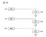
[0002] 為了在半導體元件的製造工程中之較早階段發現缺陷等,而開發一種用以不必從該晶圓切出被形成於作為基板之半導體晶圓(以下,僅稱為「晶圓」。)的半導體元件而進行檢查之元件檢查裝置即針測機。 [0003] 針測機,係具備有探針卡及平台,使探針卡之各探針接觸於檢查對象之半導體元件(Device Under Test,以下稱為「DUT」。)所具有的電極焊墊或焊錫凸塊,並使來自DUT之信號傳達至被設置於針測機上的LSI測試器,從而檢查DUT的電性特性,該探針卡,係具有多數個銷狀的探針,該平台,係載置晶圓而上下左右自如地移動(例如,參閱專利文獻1。)。 [0004] 特別是,基於提升檢查效率而使生產率提升的觀點,開發一種同時檢查被形成於晶圓之複數個DUT的電性特性之針測機。在像這樣的針測機中,係通常如圖10所示,與DUT100一一對應,設置有將電力供給至該DUT100的電源101。 [0005] 近年來,基於晶圓之大口徑化或半導體元件之生產效率提升的觀點,形成於晶圓之DUT的數量大幅增加,例如有超過1000個的情形。此時,從針測機內之配置上的限制來看,與DUT100一一對應,在針測機設置電源101較為困難,進而使針測機的成本上升。又,雖亦有在LSI測試器設置電源101的情形,但在該情況下,從LSI測試器內之配置上的限制來看,與DUT100一一對應,在LSI測試器設置電源101較為困難,進而使LSI測試器的成本上升。 [0006] 因此,如圖11所示,有研究探討出從1個電源101將電力供給至複數個DUT100。在該情況下,為了控制被供給至各DUT100的電力,雖對應於各DUT100地設置有電力供給電路102,但由於被供給至各DUT100的電力不足,進而有各DUT100之施加電壓降低的可能性,因此,電力供給電路102,係具有用以使從電源101所供給之電力放大的運算放大器。 [0007] 然而,以往,由於流過DUT100的電流(以下,稱為「元件電流」),係與流過電源101的電流等值,因此,雖使用電源101所具有的電流測定機能,將流過電源101的電流作為元件電流進行了測定,但在設置有電力供給電路102的情況下,由於運算放大器介設於電源101及DUT100之間,因此,元件電流與流過電源101的電流不會成為等值。因此,在電力供給電路102中,如圖12所示,必需在運算放大器103及DUT100之間配置感測放大器104或AD轉換器105,並使用感測放大器104或AD轉換器105來直接測定從運算放大器103流向DUT100的電流。 [先前技術文獻] [專利文獻] [0008] [專利文獻1]日本特開平7―297242號公報[0002] In order to find defects and the like at an early stage in the manufacturing process of semiconductor elements, a semiconductor wafer (hereinafter, simply referred to as "wafer") that is formed on a substrate without cutting out the wafer has been developed. .) is a device inspection device that inspects semiconductor components, that is, a needle tester. [0003] The probe tester is equipped with a probe card and a platform, so that each probe of the probe card is brought into contact with the electrode pads of the semiconductor device (Device Under Test, hereinafter referred to as "DUT") to be inspected. Or solder bumps, and transmit the signal from the DUT to the LSI tester installed on the probe tester to check the electrical characteristics of the DUT. The probe card has a plurality of pin-shaped probes. The platform , The wafer is placed and moved freely up and down, left and right (for example, refer to Patent Document 1). [0004] In particular, based on the viewpoint of improving inspection efficiency and increasing productivity, a needle tester was developed to simultaneously inspect the electrical characteristics of a plurality of DUTs formed on a wafer. In such a needle tester, as shown in FIG. 10, a
[本發明所欲解決之課題] [0009] 然而,感測放大器104或AD轉換器105,係必需對應於1個DUT100地逐一設置,在如上述般之形成於晶圓的DUT之數量超過1000個的情況下,從針測機內之配置上的限制來看,與DUT的數量對應,設置等量的感測放大器104或AD轉換器105較為困難,其結果,難以測定流過多數個DUT的電流。又,多數個感測放大器104或AD轉換器105的存在會產生使針測機之成本上升的問題。 [0010] 本發明之目的,係在於提供一種可不使成本上升而測定流過多數個元件的電流之元件檢查電路、元件檢查裝置及探針卡。 [用以解決課題之手段] [0011] 為了達成上述目的,本發明之元件檢查電路,係具備有具有電流測定機能的電源、運算放大器及第1電阻,依前述電源、前述運算放大器、前述第1電阻及元件該順序串聯連接,並將前述電源連接於前述運算放大器的非反相輸入端子,該元件檢查電路,其特徵係,更具備有:第1回授流路,將前述第1電阻及前述元件之間的電壓施加至前述運算放大器的反相輸入端子;及第2回授流路,連接前述運算放大器及前述第1電阻之間的點和前述運算放大器的非反相輸入端子,前述第2回授流路,係具有第2電阻。 [發明之效果] [0012] 根據本發明,由於第1電阻及元件之間的電壓被施加至運算放大器的反相輸入端子,因此,藉由運算放大器之負回授動作,運算放大器之非反相輸入端子的電位成為與第1電阻及元件之間的電位相等。又,由於第2回授流路,係連接運算放大器及第1電阻之間的點和運算放大器的非反相輸入端子,因此,第2回授流路之電壓下降量,係與第1電阻之電壓下降量相等。而且,流過第2回授流路的電流,係可使用電源所具有的電流測定機能來進行測定。因此,藉由歐姆定律,可基於流過第1電阻、第2電阻及第2回授流路之電流,計算流過第1電阻的電流。其結果,可不必與各元件對應地設置感測放大器或AD轉換器,而計算從第1電阻流向元件的電流。亦即,不使成本上升而可測定流過多數個元件的電流。[Problem to be solved by the present invention] [0009] However, the
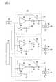
[0014] 以下,參閱圖面,說明關於本發明之實施形態。 [0015] 首先,說明關於本發明之第1實施形態。 [0016] 圖1,係用以概略地說明作為本實施形態之元件檢查裝置之針測機之構成的立體圖;圖2,係同正視圖。圖2,係部分地描繪成剖面圖,且表示內建於後述之本體12、裝載器13及測試箱14的構成要素。 [0017] 在圖1及圖2中,針測機10,係具備有本體12、裝載器13及測試箱14,同時進行被形成於晶圓W之多數個DUT之電性特性的檢查,該本體12,係內建有載置晶圓W的平台11,該裝載器13,係被配置為鄰接於該本體12,該測試箱14,係以覆蓋本體12的方式而配置。本體12,係內部呈現空洞的殼體形狀,在該內部,係除了上述的平台11以外,另以與該平台11相對向的方式,配置有探針卡15,探針卡15,係與晶圓W相對向。探針卡15,係具有:板狀之卡板16;及探針頭17,被配置於卡板16中之與晶圓W相對向的下面。如圖3所示,探針頭17,係具有與被形成於晶圓W之各DUT的電極焊墊或焊錫凸塊對應之多數個針狀的探針18。 [0018] 晶圓W,係以使相對於平台11之相對位置不偏移的方式,被固定於該平台11。平台11,係可於水平方向及上下方向上移動,並調整探針卡15及晶圓W的相對位置,使各DUT之電極焊墊或焊錫凸塊正確地接觸於探針頭17的各探針16。裝載器13,係從搬送容器即FOUP(未圖示)取出形成有DUT的晶圓W,且載置於本體12之內部的平台11。在探針卡15的卡板16,係形成有卡側檢查電路19(參閱圖3),該卡側檢查電路19,係被連接於探針頭17。 [0019] 測試箱14,係具有配線即導線20與形成有箱側檢查電路21(元件檢查電路)的測試板22。導線20,係連接測試箱14的測試板22與探針卡15的卡板16。在針測機10中,係藉由卡側檢查電路19或箱側檢查電路21,重現安裝有半導體元件之母板之電路構成的一部分。裝載器13,係內建有由電源、控制器或簡單的測定模組所構成的基座單元23。基座單元23,係藉由配線24而連接於箱側檢查電路21,控制器,係指示開始對箱側檢查電路21進行DUT之電性特性的檢查。 [0020] 在進行DUT之電性特性的檢查之際,箱側檢查電路21,係經由卡側檢查電路19或探針卡15將電力供給至各DUT,並且將數據發送至卡側檢查電路19。而且,箱側檢查電路21,係基於來自卡側檢查電路19的電信號,判定所發送的數據是否被與各DUT連接點的卡側檢查電路19正確處理。 [0021] 圖4,係表示圖2中之箱側檢查電路之構成的電路圖。另外,在圖4中,係僅表示關於電力之供給的構成要素。 [0022] 在圖4中,箱側檢查電路21,係具有:電源25,具有電流測定機能;複數個電力供給電路27,一對一地被連接於形成在晶圓W的各DUT26;及開關控制部28。電源25,係被分歧而連接於複數個電力供給電路27,來自電源25的電力被分配供給至各電力供給電路27。各電力供給電路27,係具有運算放大器29與感測電阻30(第1電阻),在箱側檢查電路21中,係依電源25、運算放大器29、感測電阻30、探針18及DUT26該順序串聯連接,電源25,係被連接於運算放大器29的非反相輸入端子,運算放大器29,係放大來自被分配供給至該電力供給電路27之電源25的電力,且供給至DUT26。而且,各電力供給電路27,係具有:負回授流路32(第1回授流路),連接存在於感測電阻30及DUT26之間的下游感測點31和運算放大器29的反相輸入端子;及正回授流路34(第2回授流路),連接存在於運算放大器29及感測電阻30之間的上游感測點33和運算放大器29的非反相輸入端子。 [0023] 負回授流路32,係將下游感測點31之電壓,亦即感測電阻30及DUT26之間的電壓施加至運算放大器29的反相輸入端子。正回授流路34,係具有回授電阻35(第2電阻)與可藉由開關動作來切斷正回授流路34的開關36,開關36,係被連接於開關控制部28,開關控制部,係控制開關36的開關動作。另外,開關36,係通常被設成為關閉。 [0024] 在箱側檢查電路21中,如上述般,由於下游感測點31之電壓被施加至運算放大器29的反相輸入端子,因此,藉由負回授動作,運算放大器29之非反相輸入端子的電位,係成為與運算放大器29之反相輸入端子的電位亦即下游感測點31的電位相等。 [0025] 另一方面,在箱側檢查電路21中,當開關36被設成為開啟時,雖連接有上游感測點33及運算放大器29的非反相輸入端子,但由於運算放大器29之非反相輸入端子的電位,係與下游感測點31的電位相等,因此,正回授流路34之電壓下降量,係成為與上游感測點33之電位及下游感測點31之電位的差,亦即感測電阻30之電壓下降量相等。在此,當將感測電阻30之電阻值設成為R1(Ω),將流過感測電阻30之電流設成為I1(A),將回授電阻35之電阻值設成為R2(Ω),將流過回授電阻35的電流設成為I2(A)時,則由於藉由歐姆定律,感測電阻30之電壓下降量,係成為I1×R1(V),正回授流路34之電壓下降量,係成為I2×R2(V),因此,下述式(1)成立。 I1×R1= I2×R2…(1) [0026] 在此,感測電阻30之電阻值R1、回授電阻35之電阻值R2為已知,流過正回授流路34的電流(以下,稱為「回授電流」。)I2,係可使用電源25所具有的電流測定機能來進行計測。因此,流過感測電阻30的電流,亦即流過DUT26的電流(以下,稱為「元件電流」。)I1,係可基於下述式(2)加以計算。 I1= I2×R2/R1…(2) [0027] 由以上可知,在箱側檢查電路21中,係可不必與各DUT26對應地設置感測放大器或AD轉換器,而計算流過感測電阻30的元件電流。亦即,可不使針測機之成本上升,而測定流過被形成於晶圓W之多數個DUT26的電流。 [0028] 又,由於在箱側檢查電路21中,係1個電源25被連接於複數個電力供給電路27之運算放大器29的非反相輸入端子,複數個電力供給電路27被一對一地連接於複數個DUT26,因此,可從1個電源25將電力供給至複數個DUT26,並且可減少電源25的數量而進一步減少成本。 [0029] 而且,在箱側檢查電路21中,雖係藉由電源25的電流測定機能來計測各電力供給電路27的正回授流路34中之回授電流I2,但由於1個電源25,係被連接於複數個電力供給電路27,因此,存在有電源25同時計測複數個回授電流I2,在各電力供給電路27中,由於正回授流路34,係具有開關36,因此,可藉由控制各正回授流路34中之開關36的動作之方式,使回授電流I2僅在1個正回授流路34流動,其結果,可防止電源25同時計測複數個回授電流I2。又,藉由使各電力供給電路27中之正回授流路34的開關36之各個依序成為開啟的方式,可依序計測所有電力供給電路27中之回授電流I2,其結果,可計算所有DUT26的元件電流。 [0030] 另外,在圖4中,雖係在箱側檢查電路21中表示1個電源25,但箱側檢查電路21所具有之電源25的數量並不限於1個。又,在圖4中,雖係在電源25連接有3個電力供給電路27,但被連接於電源25之電力供給電路27的數量並不限於3個。 [0031] 其次,說明關於本發明之第2實施形態。 [0032] 由於第2實施形態,係基本上其構成、作用與上述的第1實施形態相同,因此,關於重複之構成、作用,係省略說明,在下述中,進行關於不同之構成、作用的說明。 [0033] 圖5,係表示本發明之第2實施形態之元件檢查電路中之電力供給電路之構成的電路圖。 [0034] 吾人認為,在計算DUT26待機時之元件電流I1之際,由於待機時之元件電流I1微弱,因此,感測電阻30之電壓下降量亦即正回授流路34之電壓下降量變小,且回授電流I2亦變小。在該情況下,回授電流I2的計測精度會下降,其結果,恐有元件電流I1的計算精度下降之虞。對應於此,考慮將感測電阻30之電阻值R1儘可能設定為較大。然而,在DUT26作動時,雖係流動有比待機時大的元件電流I1,但當將感測電阻30之電阻值R1儘可能設定為較大時,則元件電流I1變得難以流過感測電阻30,而恐有難以將足夠的電力供給至DUT26之虞。 [0035] 在本實施形態中,係對應於此,電力供給電路37具有:旁通流路38(迴避流路),迴避感測電阻30而直接連接運算放大器29及DUT26。該旁通流路38,係具有二極體39,該二極體39,係與感測電阻30並聯連接。又,二極體39,係當感測電阻30之電壓下降量,亦即被施加至二極體39之電壓的電位差成為預定值以上時,使電流急遽地通過。藉此,在DUT26作動時,當比較大的元件電流I1欲通過感測電阻30而感測電阻30之電壓下降量變大時,元件電流I1,係繞過感測電阻30流過旁通流路38而直接到達DUT26。其結果,即便將感測電阻30之電阻值R1儘可能設定為較大,亦可在DUT26作動時,使比較大的元件電流I1經由旁通流路38而流向DUT26,並且可將足夠的電力供給至作動的DUT26。 [0036] 其次,說明關於本發明之第3實施形態。 [0037] 由於第3實施形態,係基本上其構成、作用與上述的第2實施形態相同,因此,關於重複之構成、作用,係省略說明,在下述中,進行關於不同之構成、作用的說明。 [0038] 圖6,係表示本發明之第3實施形態之元件檢查電路中之電力供給電路之構成的電路圖。 [0039] 如第2實施形態所述,為了抑制DUT26待機時之元件電流I1之計算的下降,當將感測電阻30之電阻值R1儘可能設定為較大時,恐有無法將足夠的電力供給至DUT26之虞。在本實施形態中,係對應於此,電力供給電路40具有:電晶體41,由雙極性電晶體所構成;及未圖示的附加電源(其他電源),供給比較大的電力。電晶體41的基極,係被連接於運算放大器29及感測電阻30之間,並且電晶體41的射極,係被連接於感測電阻30及DUT26之間。亦即,電晶體41與感測電阻30並聯配置。因此,在電晶體41的基極及射極之間會產生相當於感測電阻30之電壓下降量的電位差,而流動有基極電流。又,電晶體41的集極,係經由限制電路42(電流限制電路)而連接有附加電源。藉此,在DUT26作動時,當比較大的元件電流I1欲通過感測電阻30而感測電阻30之電壓下降量變大時,則基極電流流過電晶體41而電晶體41成為開啟,並經由電晶體41,從附加電源將比較大的電力供給至DUT26。其結果,即便將感測電阻30之電阻值R1儘可能設定為較大,亦可將足夠的電力供給至作動時的DUT26。 [0040] 又,由於在附加電源及電晶體41之間,係介設有限制電路42,因此,即便DUT26短路,亦可防止大電流從附加電源朝向DUT26流動的情形,並且可防止DUT26被破壞的情形。 [0041] 另外,在電力供給電路40中,雖係使用了雙極性電晶體作為電晶體41,但亦可使用場效應電晶體。在該情況下,電晶體41的閘極,係被連接於運算放大器29及感測電阻30之間,並且電晶體41的源極,係被連接於感測電阻30及DUT26之間。而且,電晶體41的汲極,係經由限制電路42而連接有附加電源。 [0042] 其次,說明關於本發明之第4實施形態。 [0043] 由於第4實施形態,係基本上其構成、作用與上述的第1實施形態相同,因此,關於重複之構成、作用,係省略說明,在下述中,進行關於不同之構成、作用的說明。 [0044] 圖7,係表示本發明之第4實施形態之元件檢查電路中之電力供給電路之構成的電路圖。 [0045] 如上述般,在箱側檢查電路21中,雖係由1個電源25將電力分配供給至複數個DUT26,但在複數個DUT26中之1個DUT26發生了問題的情況下,由於當將電力持續供給至該DUT26時,恐有該DUT26被破壞之虞,因此,電源25,係必需中止電力的供給,從而中止對發生了問題的DUT26供給電力。然而,當中止來自電源25之電力的供給時,由於對其他DUT26之電力的供給亦會被中止,因此,恐有無法檢查未發生問題之其他DUT26的電性特性,從而導致各DUT26的檢查效率下降之虞。 [0046] 在本實施形態中,係對應於此,電力供給電路43具有:附加開關44(其他開關),介設於運算放大器29及感測電阻30之間。藉此,在DUT26發生了問題的情況下,不必中止來自電源25之電力的供給,可僅使附加開關44成為關閉而防止對發生了問題之DUT26供給電力的情形。藉此,可防止無法檢查未發生問題之其他DUT26的電性特性之情形,並可防止各DUT26之檢查效率下降。 [0047] 又,電力供給電路43,係具有介設於該附加開關44及感測電阻30之間的輔助電阻45(第3電阻),上游感測點33,係被配置於輔助電阻45及感測電阻30之間。藉此,正回授流路34之電壓下降量,係成為因輔助電阻45而下降的電位與運算放大器29之非反相輸入端子的電位之差。亦即,可減少正回授流路34之電壓下降量,並例如可防止過大之電流流過正回授流路34而使回授電阻35異常發熱的情形。而且,在電力供給電路43中,係除了感測電阻30以外,輔助電阻45與運算放大器29串聯連接。藉此,可限制流向運算放大器29的電流,並且可防止過大的電流流過運算放大器29而使運算放大器29異常發熱的情形。 [0048] 另外,在電力供給電路43中,雖係依運算放大器29、附加開關44、輔助電阻45及感測電阻30該順序串聯連接,但只要上游感測點33被配置於輔助電阻45及感測電阻30之間,則亦可交換附加開關44及輔助電阻45的順序。 [0049] 其次,說明關於本發明之第5實施形態。 [0050] 由於第5實施形態,係基本上其構成、作用與上述的第1實施形態相同,因此,關於重複之構成、作用,係省略說明,在下述中,進行關於不同之構成、作用的說明。 [0051] 圖8,係表示本發明之第5實施形態之元件檢查電路中之電力供給電路之構成的電路圖。 [0052] 如上述般,在箱側檢查電路21中,雖係由1個電源25將電力分配供給至複數個DUT26,但當由1個電源25供給電力之DUT26的數量增加時,即便在各DUT26待機時可將足夠的電力供給至各DUT26,但在各DUT26作動時恐有無法將足夠的電力供給至各DUT26之虞。 [0053] 在本實施形態中,係對應於此,電力供給電路46具有:電晶體47,由雙極性電晶體所構成;及未圖示的附加電源,供給比較大的電力。電晶體47,係介設於運算放大器29及感測電阻30之間,電晶體47的基極被連接於運算放大器29,並且電晶體47的射極被連接於感測電阻30。因此,在電晶體41的基極及射極之間,係基極電流因運算放大器29及感測電阻30的電位差而流動。又,電晶體47的集極,係經由限制電路48而連接有其他附加電源。藉此,為了在DUT26作動時,使比較大的元件電流I1流過,當運算放大器29及感測電阻30的電位差變大時,則基極電流流過電晶體47而電晶體47成為開啟,並經由電晶體47,從其他附加電源將比較大的電力供給至DUT26。其結果,即便為由1個電源25將電力分配供給至多數的DUT26之情況下,亦可將足夠的電力供給至作動時之DUT26。 [0054] 另外,在電力供給電路46中,雖係使用了雙極性電晶體作為電晶體47,但亦可使用場效應電晶體。在該情況下,電晶體47的閘極,係被連接於運算放大器29,並且電晶體47的源極,係被連接於感測電阻30。又,電晶體47的汲極,係經由限制電路48而連接有其他附加電源。 [0055] 以上,雖使用上述各實施形態說明了關於本發明,但本發明並不限定於上述各實施形態者。 [0056] 例如,即便為從1個電源25將電力僅供給至1個DUT26的情況下,亦存在有在電源25的供給電力較小時,使用運算放大器29來放大供給電力的情形。此時,雖亦使用具有與電力供給電路40大致相同構成的電力供給電路49,但由於電源25沒有同時計測複數個回授電流I2的可能性,因此,在電力供給電路49中,係如圖9所示,無需在正回授流路34設置開關36,而且,亦無需設置開關控制部28。藉此,與電力供給電路40相比,可簡化電力供給電路49的構成。 [0057] 又,在上述的各實施形態中,雖係在測試箱14的箱側檢查電路21形成有電力供給電路27(37,40,43,46,49),但亦可在探針卡15的卡側檢查電路19形成電力供給電路(37,40,43,46,49)。[0014] Hereinafter, referring to the drawings, the embodiments of the present invention will be described. [0015] First, the first embodiment of the present invention will be described. [0016] FIG. 1 is a perspective view schematically illustrating the structure of a needle tester as a component inspection device of this embodiment; FIG. 2 is the same front view. picture. FIG. 2 is partially depicted as a cross-sectional view, and shows the constituent elements built in the
[0058]W‧‧‧晶圓10‧‧‧針測機14‧‧‧測試箱15‧‧‧探針卡19‧‧‧卡側檢查電路21‧‧‧箱側檢查電路25‧‧‧電源26‧‧‧DUT27、37、40、43、46、49‧‧‧電力供給電路29‧‧‧運算放大器30‧‧‧感測電阻32‧‧‧負回授流路33‧‧‧上游感測點34‧‧‧正回授流路35‧‧‧回授電阻36‧‧‧開關38‧‧‧旁通流路41、47‧‧‧電晶體42、48‧‧‧限制電路44‧‧‧附加開關45‧‧‧輔助電阻[0058]W‧‧‧
[0013] [圖1]用以概略地說明作為本發明之第1實施形態之元件檢查裝置之針測機之構成的立體圖。 [圖2]用以概略地說明圖1之針測機之構成的正視圖。 [圖3]表示圖2中之探針卡之構成的放大正視圖。 [圖4]表示圖2中之箱側檢查電路之構成的電路圖。 [圖5]表示本發明之第2實施形態之元件檢查電路中之電力供給電路之構成的電路圖。 [圖6]表示本發明之第3實施形態之元件檢查電路中之電力供給電路之構成的電路圖。 [圖7]表示本發明之第4實施形態之元件檢查電路中之電力供給電路之構成的電路圖。 [圖8]表示本發明之第5實施形態之元件檢查電路中之電力供給電路之構成的電路圖。 [圖9]表示從1個電源將電力僅供給至1個DUT的情況之電力供給電路之構成的電路圖。 [圖10]用以說明以往的針測機中之電源及DUT之對應關係的電路圖。 [圖11]用以說明從1個電源將電力供給至複數個DUT的情況下之電源及各DUT之對應關係的電路圖。 [圖12]表示從1個電源將電力供給至複數個DUT的情況下之通常的電力供給電路之構成的電路圖。[0013] [FIG. 1] A perspective view for schematically explaining the structure of a needle tester as a component inspection device of the first embodiment of the present invention. [Fig. 2] A front view for schematically explaining the structure of the needle measuring machine in Fig. 1. [Fig. 3] shows an enlarged front view of the structure of the probe card in Fig. 2. [Fig. 4] A circuit diagram showing the structure of the box side inspection circuit in Fig. 2. [FIG. 5] A circuit diagram showing the configuration of the power supply circuit in the component inspection circuit of the second embodiment of the present invention. [FIG. 6] A circuit diagram showing the configuration of the power supply circuit in the component inspection circuit of the third embodiment of the present invention. [FIG. 7] A circuit diagram showing the configuration of the power supply circuit in the component inspection circuit of the fourth embodiment of the present invention. [FIG. 8] A circuit diagram showing the configuration of the power supply circuit in the component inspection circuit of the fifth embodiment of the present invention. [Figure 9] shows a circuit diagram of the configuration of the power supply circuit when the power is supplied from one power source to one DUT only. [Figure 10] A circuit diagram used to illustrate the corresponding relationship between the power supply and the DUT in the conventional needle tester. [Figure 11] A circuit diagram for explaining the power supply and the correspondence between the DUTs when power is supplied from one power supply to a plurality of DUTs. [FIG. 12] A circuit diagram showing the structure of a normal power supply circuit when power is supplied from one power supply to a plurality of DUTs.
18‧‧‧探針18‧‧‧Probe
21‧‧‧箱側檢查電路21‧‧‧Box side inspection circuit
25‧‧‧電源25‧‧‧Power
26‧‧‧DUT26‧‧‧DUT
27‧‧‧電力供給電路27‧‧‧Power supply circuit
28‧‧‧開關控制部28‧‧‧Switch Control Unit
29‧‧‧運算放大器29‧‧‧Operational amplifier
30‧‧‧感測電阻30‧‧‧Sensing resistance
31‧‧‧下游感測點31‧‧‧Downstream sensing point
32‧‧‧負回授流路32‧‧‧Negative feedback flow path
33‧‧‧上游感測點33‧‧‧Upstream sensing point
34‧‧‧正回授流路34‧‧‧Positive feedback flow path
35‧‧‧回授電阻35‧‧‧Feedback resistor
36‧‧‧開關36‧‧‧Switch
Claims (9)
Translated fromChineseApplications Claiming Priority (2)
| Application Number | Priority Date | Filing Date | Title |
|---|---|---|---|
| JP2016-158906 | 2016-08-12 | ||
| JP2016158906AJP6738236B2 (en) | 2016-08-12 | 2016-08-12 | Device inspection circuit, device inspection device and probe card |
Publications (2)
| Publication Number | Publication Date |
|---|---|
| TW201821817A TW201821817A (en) | 2018-06-16 |
| TWI738842Btrue TWI738842B (en) | 2021-09-11 |
Family
ID=61161863
Family Applications (1)
| Application Number | Title | Priority Date | Filing Date |
|---|---|---|---|
| TW106127068ATWI738842B (en) | 2016-08-12 | 2017-08-10 | Component inspection circuit, component inspection device and probe card |
Country Status (6)
| Country | Link |
|---|---|
| US (1) | US10859601B2 (en) |
| JP (1) | JP6738236B2 (en) |
| KR (1) | KR102157449B1 (en) |
| CN (1) | CN109564262B (en) |
| TW (1) | TWI738842B (en) |
| WO (1) | WO2018029971A1 (en) |
Families Citing this family (8)
| Publication number | Priority date | Publication date | Assignee | Title |
|---|---|---|---|---|
| US11324100B2 (en)* | 2018-01-24 | 2022-05-03 | Seiko Epson Corporation | Light source apparatus and projection-type display apparatus |
| US12306245B2 (en)* | 2020-01-02 | 2025-05-20 | Texas Instruments Incorporated | On-chip current sensor |
| JP2022091378A (en)* | 2020-12-09 | 2022-06-21 | 東京エレクトロン株式会社 | Power supply and inspection equipment |
| TWI770740B (en)* | 2020-12-28 | 2022-07-11 | 致茂電子股份有限公司 | Electronic load apparatus |
| JP7632974B2 (en) | 2021-07-02 | 2025-02-19 | 東京エレクトロン株式会社 | Inspection device and inspection method |
| US20230104095A1 (en)* | 2021-10-04 | 2023-04-06 | Nanya Technology Corporation | Testing device and method for testing devices under test |
| CN114624498A (en)* | 2022-03-10 | 2022-06-14 | 珠海市运泰利自动化设备有限公司 | Low current test system |
| CN119413221A (en)* | 2024-12-31 | 2025-02-11 | 中国计量大学 | A photoelectric sensor module detection device and method based on variable resistance matrix |
Citations (3)
| Publication number | Priority date | Publication date | Assignee | Title |
|---|---|---|---|---|
| JPH0641174Y2 (en)* | 1985-07-31 | 1994-10-26 | 株式会社アドバンテスト | Voltage-current measuring device |
| JPH11153641A (en)* | 1997-11-21 | 1999-06-08 | Ando Electric Co Ltd | Semiconductor device testing device |
| TW201617633A (en)* | 2014-08-01 | 2016-05-16 | Tokyo Electron Ltd | Device inspection method, probe card, interposer, and inspection apparatus |
Family Cites Families (16)
| Publication number | Priority date | Publication date | Assignee | Title |
|---|---|---|---|---|
| JPS6041174Y2 (en)* | 1982-04-13 | 1985-12-13 | コクヨ株式会社 | Small items display shelf |
| JPH0611509Y2 (en)* | 1986-05-02 | 1994-03-23 | 株式会社アドバンテスト | Matrix switch circuit |
| JP2660889B2 (en)* | 1992-09-08 | 1997-10-08 | ソニー・テクトロニクス株式会社 | Power supply current measuring device |
| CN2139715Y (en)* | 1992-10-14 | 1993-08-04 | 高海燕 | Frequency-modulation voltage-stabilizing energy-saving power supply controller |
| JP3156192B2 (en) | 1994-04-19 | 2001-04-16 | 東京エレクトロン株式会社 | Probe method and apparatus |
| JP3072880B2 (en)* | 1994-06-02 | 2000-08-07 | 株式会社アドバンテスト | Voltage generator for IC test |
| JP3508489B2 (en)* | 1997-07-29 | 2004-03-22 | 安藤電気株式会社 | Calibration device for programmable comparator |
| JP4594474B2 (en)* | 2000-02-10 | 2010-12-08 | 株式会社アドバンテスト | Constant voltage power supply circuit and test apparatus |
| JP2003167025A (en)* | 2001-11-30 | 2003-06-13 | Hitachi Electronics Eng Co Ltd | Power supply for semiconductor test equipment |
| US6563352B1 (en)* | 2002-03-29 | 2003-05-13 | Teradyne, Inc. | Driver circuit employing high-speed tri-state for automatic test equipment |
| JP3901698B2 (en)* | 2004-03-26 | 2007-04-04 | ローム株式会社 | Semiconductor integrated circuit with current detection function and power supply device using the same |
| JP2005315729A (en)* | 2004-04-28 | 2005-11-10 | Advantest Corp | Direct-current testing device |
| US6956393B1 (en)* | 2004-05-26 | 2005-10-18 | Advantest Corporation | Source current measurement apparatus and test apparatus |
| CN2720457Y (en)* | 2004-07-19 | 2005-08-24 | 山东博特光电技术有限公司 | Semiconductor laser characteristic parameter testing device |
| US7560947B2 (en)* | 2005-09-28 | 2009-07-14 | Teradyne, Inc. | Pin electronics driver |
| CN203422416U (en)* | 2013-08-29 | 2014-02-05 | 北京经纬恒润科技有限公司 | High-end current detection circuit |
- 2016
- 2016-08-12JPJP2016158906Apatent/JP6738236B2/enactiveActive
- 2017
- 2017-06-06CNCN201780049479.XApatent/CN109564262B/enactiveActive
- 2017-06-06USUS16/324,733patent/US10859601B2/enactiveActive
- 2017-06-06WOPCT/JP2017/021556patent/WO2018029971A1/ennot_activeCeased
- 2017-06-06KRKR1020197005930Apatent/KR102157449B1/enactiveActive
- 2017-08-10TWTW106127068Apatent/TWI738842B/enactive
Patent Citations (3)
| Publication number | Priority date | Publication date | Assignee | Title |
|---|---|---|---|---|
| JPH0641174Y2 (en)* | 1985-07-31 | 1994-10-26 | 株式会社アドバンテスト | Voltage-current measuring device |
| JPH11153641A (en)* | 1997-11-21 | 1999-06-08 | Ando Electric Co Ltd | Semiconductor device testing device |
| TW201617633A (en)* | 2014-08-01 | 2016-05-16 | Tokyo Electron Ltd | Device inspection method, probe card, interposer, and inspection apparatus |
Also Published As
| Publication number | Publication date |
|---|---|
| JP6738236B2 (en) | 2020-08-12 |
| JP2018025519A (en) | 2018-02-15 |
| US10859601B2 (en) | 2020-12-08 |
| KR20190035815A (en) | 2019-04-03 |
| CN109564262B (en) | 2021-03-05 |
| CN109564262A (en) | 2019-04-02 |
| US20190178913A1 (en) | 2019-06-13 |
| WO2018029971A1 (en) | 2018-02-15 |
| TW201821817A (en) | 2018-06-16 |
| KR102157449B1 (en) | 2020-09-17 |
Similar Documents
| Publication | Publication Date | Title |
|---|---|---|
| TWI738842B (en) | Component inspection circuit, component inspection device and probe card | |
| JP6496292B2 (en) | How to expand tester drive and measurement capabilities | |
| JP4774071B2 (en) | Probe resistance measurement method and semiconductor device having probe resistance measurement pad | |
| TWI518332B (en) | Wafer level probe card assembly | |
| US9391447B2 (en) | Interposer to regulate current for wafer test tooling | |
| TWI572861B (en) | Semiconductor module, electrical connector and inspection device | |
| JP2019060768A (en) | Resistance measurement apparatus, substrate inspection apparatus, and resistance measurement method | |
| TWI539166B (en) | Check the wafer and test system | |
| TWI649566B (en) | Substrate inspection device | |
| US8624615B2 (en) | Isolation circuit | |
| TWI383160B (en) | Electrical connection defect detection system and method | |
| CN108279325A (en) | Probe card module for testing circuit chip | |
| CN113748496A (en) | Testing device | |
| JP2007315789A (en) | Semiconductor integrated circuit and mounting inspection method thereof | |
| CN102967769B (en) | Measurement mechanism with for measuring the method that chip is connected to chip carrier | |
| JPH10199943A (en) | Method of testing semiconductor integrated circuit and probe card | |
| JP2008187024A (en) | Probe card and probe card system | |
| JP2007198930A (en) | Semiconductor inspection system and semiconductor device | |
| JP2002334966A (en) | Multi-chip module and inspection method therefor | |
| JP6255833B2 (en) | Substrate inspection method and substrate inspection apparatus | |
| JP2009065037A (en) | Semiconductor integrated circuit and its inspection device | |
| TW202411670A (en) | Detection circuit | |
| CN118294705A (en) | Detection method of detection circuit | |
| TW201105981A (en) | Power signal detection module | |
| JP2015230179A (en) | Board inspection equipment |