Movatterモバイル変換


[0]ホーム

URL:


TWI735566B - Apparatus for measuring condition of electroplating cell components and associated methods - Google Patents

Apparatus for measuring condition of electroplating cell components and associated methods
Download PDF

Info

Publication number
TWI735566B
TWI735566BTW106112701ATW106112701ATWI735566BTW I735566 BTWI735566 BTW I735566BTW 106112701 ATW106112701 ATW 106112701ATW 106112701 ATW106112701 ATW 106112701ATW I735566 BTWI735566 BTW I735566B
Authority
TW
Taiwan
Prior art keywords
conductive
conductive pads
measuring
semiconductor processing
processing equipment
Prior art date
Application number
TW106112701A
Other languages
Chinese (zh)
Other versions
TW201802468A (en
Inventor
馬克 E 艾默生
史蒂芬 T 邁爾
勞倫斯 奧索夫斯基
Original Assignee
美商蘭姆研究公司
Priority date (The priority date is an assumption and is not a legal conclusion. Google has not performed a legal analysis and makes no representation as to the accuracy of the date listed.)
Filing date
Publication date
Application filed by 美商蘭姆研究公司filedCritical美商蘭姆研究公司
Publication of TW201802468ApublicationCriticalpatent/TW201802468A/en
Application grantedgrantedCritical
Publication of TWI735566BpublicationCriticalpatent/TWI735566B/en

Links

Images

Classifications

Landscapes

Abstract

A device for measuring electrical properties of electrical contacts within an electroplating apparatus has a disc-shaped structure like that of a wafer. Multiple conductive pads are formed to collectively circumscribe an outer periphery of the disc-shaped structure. Adjacently positioned ones of the conductive pads are electrically isolated from each other. The device includes a current source that supplies electric current at a first terminal and sinks electric current at a second terminal. The device includes measurement circuitry, having first and second input terminals, that determines a value of an electrical parameter based on signals present at the first and second input terminals. The device includes switching circuitry for connecting selected ones of the conductive pads to the first and second terminals of the current source and to the first and second input terminals of the measurement circuitry at a given time. The device also includes an onboard power supply.

Description

Translated fromChinese
量測電鍍槽元件之狀態的設備與相關方法Equipment and related methods for measuring the state of electroplating bath components

本發明關於半導體元件製造。The present invention relates to semiconductor device manufacturing.

一些半導體裝置製造製程包含將材料電鍍至半導體晶圓(以下稱「晶圓」)之上。電鍍可在電鍍槽中進行,其中具有導電晶種層存在於其上的晶圓係配置成物理接觸繞晶圓周緣配置的多個電接觸件。此外,在一些配置中,當晶圓係配置成物理接觸多個電接觸件時,晶圓亦也配置成使得晶圓的周緣部分物理接觸唇封構件,以盡可能防止電鍍溶液到達該多個電接觸件。在此等配置中,在晶圓與唇封構件之間的密封可能不是完美的,且可能隨著多次電鍍循環而劣化,從而不利地允許一些量的電鍍溶液到達一些電接觸件。Some semiconductor device manufacturing processes involve electroplating materials onto semiconductor wafers (hereinafter referred to as "wafers"). The electroplating can be carried out in an electroplating bath, in which the wafer with the conductive seed layer present thereon is arranged to physically contact a plurality of electrical contacts arranged around the periphery of the wafer. In addition, in some configurations, when the wafer system is configured to physically contact multiple electrical contacts, the wafer is also configured such that the peripheral portion of the wafer physically contacts the lip seal member to prevent the electroplating solution from reaching the multiple electrical contacts as much as possible. Electrical contacts. In these configurations, the seal between the wafer and the lip seal member may not be perfect and may deteriorate with multiple electroplating cycles, thereby disadvantageously allowing some amount of electroplating solution to reach some electrical contacts.

電流係以受控制的方式被引導流經多個電接觸件,以使在晶圓上存在的晶種層帶電,且從而誘發導致將材料電鍍在晶圓上的反應。隨著電鍍循環的數目增加,電鍍材料可能積聚在一些電接觸件上及/或在唇封構件上,且導致在沿延伸至晶圓之一個以上導電路徑的電阻發生變化。沿著通至晶圓之一給定導電路徑之電阻的變化可能影響在晶圓上的電鍍結果。舉例而言,沿者通至晶圓之一給定導電路徑之增加的電阻可能減少沿該給定導電路徑之電流的量,及導致在晶圓上對應於該給定導電路徑之物理接觸位置附近之電鍍材料的量(例如厚度)局部減少。The current is directed to flow through a plurality of electrical contacts in a controlled manner to charge the seed layer present on the wafer and thereby induce a reaction that leads to the plating of the material on the wafer. As the number of electroplating cycles increases, electroplating material may accumulate on some electrical contacts and/or on the lip seal member and cause changes in resistance along more than one conductive path extending to the wafer. Variations in resistance along a given conductive path to the wafer may affect the plating results on the wafer. For example, the increased resistance along a given conductive path leading to the wafer may reduce the amount of current along the given conductive path and result in a physical contact location on the wafer that corresponds to the given conductive path The amount of nearby plating material (such as thickness) is locally reduced.

鑑於上述情況,應理解需要識別多個電接觸件的哪一者及/或唇封構件的哪個部分已經經歷不期望的電鍍,且到達了沿相應導電路徑之電阻的變化可能不利地影響在晶圓上之電鍍結果的程度。這是本發明之內容產生的背景。In view of the above, it should be understood that it is necessary to identify which of the multiple electrical contacts and/or which part of the lip seal member has undergone undesired electroplating, and that the change in resistance along the corresponding conductive path may adversely affect the crystal The degree of electroplating results on the circle. This is the background of the content of the present invention.

在一示例實施例中,揭示一種測量在一半導體處理設備之內之導電路徑之電特性的裝置。該半導體處理設備係配置成當在一晶圓上執行一製程時,將該等導電路徑電連接至該晶圓的一表面。該裝置包含一盤狀結構,該盤狀結構的外徑實質上等於該晶圓的外徑。該盤狀結構的整體厚度實質上類似於該晶圓的整體厚度。該裝置包含沿該盤狀結構之第一側的外周緣形成的多個導電的墊。該多個導電的墊之相鄰配置者係彼此電隔離。該多個導電的墊共同界定該盤狀結構之該第一側的該外周緣。該裝置包含具有一第一端子及一第二端子的一電源。當該盤狀結構係配置在該半導體處理設備之內時,該電源係配置成經由在該第一端子與該第二端子之間延伸的一導電路徑及經由該半導體處理設備的一部分供應電功率。該第一端子係電連接至該多個導電的墊之其中至少一者的一第一集合。該第二端子係電連接至該多個導電的墊之其中至少一者的一第二集合。該多個導電的墊之該第二集合係不包括該多個導電的墊之該第一集合。該多個導電的墊之該第一及第二集合形成在該第一端子及該第二端子之間延伸之該導電路徑的一部分。該裝置包含具有一第一輸入端子及一第二輸入端子的測量電路。該測量電路的該第一輸入端子係電連接至該多個導電的墊之一選擇的第一者。該測量電路的該第二輸入端子係電連接至該多個導電的墊之一選擇的第二者。該測量電路係配置成基於在該多個導電的墊之該選擇的第一及第二者處存在的電訊號,判定一電參數的值。該裝置亦包含配置在該盤狀結構上的一電源供應器。該電源供應器係加以連接,以將電功率供應至在該盤狀結構上的所有電動元件。In an exemplary embodiment, an apparatus for measuring the electrical characteristics of a conductive path in a semiconductor processing device is disclosed. The semiconductor processing equipment is configured to electrically connect the conductive paths to a surface of the wafer when a process is performed on a wafer. The device includes a disc-shaped structure, and the outer diameter of the disc-shaped structure is substantially equal to the outer diameter of the wafer. The overall thickness of the disc-shaped structure is substantially similar to the overall thickness of the wafer. The device includes a plurality of conductive pads formed along the outer periphery of the first side of the disc-shaped structure. Adjacent configurations of the plurality of conductive pads are electrically isolated from each other. The plurality of conductive pads collectively define the outer periphery of the first side of the disc-shaped structure. The device includes a power supply with a first terminal and a second terminal. When the disc structure is disposed in the semiconductor processing device, the power supply is configured to supply electric power via a conductive path extending between the first terminal and the second terminal and via a part of the semiconductor processing device. The first terminal is electrically connected to a first set of at least one of the plurality of conductive pads. The second terminal is electrically connected to a second set of at least one of the plurality of conductive pads. The second set of the plurality of conductive pads does not include the first set of the plurality of conductive pads. The first and second sets of the plurality of conductive pads form part of the conductive path extending between the first terminal and the second terminal. The device includes a measuring circuit with a first input terminal and a second input terminal. The first input terminal of the measuring circuit is electrically connected to the first selected one of the plurality of conductive pads. The second input terminal of the measuring circuit is electrically connected to a second selected one of the plurality of conductive pads. The measurement circuit is configured to determine the value of an electrical parameter based on electrical signals present at the selected first and second ones of the plurality of conductive pads. The device also includes a power supply arranged on the disc structure. The power supply is connected to supply electric power to all electric components on the disc structure.

在一示例實施例中,揭示一種測量在一半導體處理設備之內之導電路徑之電特性的方法。該半導體處理設備係配置成當在一晶圓上執行一製程時,將該等導電路徑電連接至該晶圓的一表面。該方法包含在該半導體處理設備之內配置一測量裝置。該測量裝置具有一盤狀結構,其中該盤狀結構的外徑實質上等於該晶圓的外徑,且其中該盤狀結構的整體厚度實質上類似於該晶圓的整體厚度。該測量裝置係配置在該半導體處理設備之內,使得沿該測量裝置之第一側的外周緣形成之多個導電的墊物理接觸在該半導體處理設備之內的電接觸件。該多個導電的墊之相鄰配置者係在該測量裝置中彼此電隔離。該多個導電的墊共同界定該測量裝置之該第一側的該外周緣。該方法包含操作該測量裝置以經由一導電路徑供應電功率,該導電路徑包括該多個導電的墊之其中至少一者的一第一集合及該多個導電的墊之其中至少一者的一第二集合。該多個導電的墊之該第二集合係不包括該多個導電的墊之該第一集合。該方法包含操作該測量裝置以測量在該多個導電的墊之一選擇的第一者及在該多個導電的墊之一選擇的第二者處存在的電訊號。該方法亦包含操作該測量裝置,以使用該測量的電訊號,針對延伸穿過該半導體處理設備的一部分且包含該多個導電的墊之該選擇的第一者及該多個導電的墊之該選擇的第二者的一導電路徑,判定一特徵參數。In an exemplary embodiment, a method of measuring the electrical characteristics of a conductive path in a semiconductor processing device is disclosed. The semiconductor processing equipment is configured to electrically connect the conductive paths to a surface of the wafer when a process is performed on a wafer. The method includes arranging a measuring device in the semiconductor processing equipment. The measuring device has a disc-shaped structure, wherein the outer diameter of the disc-shaped structure is substantially equal to the outer diameter of the wafer, and the overall thickness of the disc-shaped structure is substantially similar to the overall thickness of the wafer. The measuring device is arranged in the semiconductor processing equipment so that a plurality of conductive pads formed along the outer periphery of the first side of the measuring device physically contact the electrical contacts in the semiconductor processing equipment. Adjacent configurations of the plurality of conductive pads are electrically isolated from each other in the measuring device. The plurality of conductive pads jointly define the outer periphery of the first side of the measuring device. The method includes operating the measuring device to supply electric power via a conductive path, the conductive path including a first set of at least one of the plurality of conductive pads and a first set of at least one of the plurality of conductive pads Two sets. The second set of the plurality of conductive pads does not include the first set of the plurality of conductive pads. The method includes operating the measuring device to measure electrical signals present at a first selected one of the plurality of conductive pads and a second selected one of the plurality of conductive pads. The method also includes operating the measuring device to use the measured electrical signal for the selected first one of the plurality of conductive pads and the plurality of conductive pads extending through a portion of the semiconductor processing equipment A characteristic parameter of a conductive path of the selected second one is determined.

在一示例實施例中,揭示一種測量在一半導體處理設備之內之導電路徑之電特性的系統。該半導體處理設備係配置成當在一晶圓上執行一製程時,將該等導電路徑電連接至該晶圓的一表面。該系統包含具有一盤狀結構的一測量裝置,其中該盤狀結構的外徑實質上等於該晶圓的外徑,且其中該盤狀結構的整體厚度實質上類似於該晶圓的整體厚度。該測量裝置包含多個導電的墊,該多個導電的墊沿該盤狀結構之第一側的外周緣加以形成。該多個導電的墊之相鄰配置者係彼此電隔離。該多個導電的墊共同界定該盤狀結構之該第一側的該外周緣。該測量裝置包含一電源,該電源具有一第一端子及一第二端子。當該測量裝置係配置在該半導體處理設備之內時,該電源係配置成經由在該第一端子與該第二端子之間延伸的一導電路徑及經由該半導體處理設備的一部分供應電功率。該第一端子係電連接至該多個導電的墊之其中至少一者的一第一集合。該第二端子係電連接至該多個導電的墊之其中至少一者的一第二集合。該多個導電的墊之該第二集合係不包括該多個導電的墊之該第一集合。該多個導電的墊之該第一及第二集合形成在該第一端子及該第二端子之間延伸之該導電路徑的一部分。該測量裝置亦包含測量電路,該測量電路具有一第一輸入端子及一第二輸入端子。該測量電路的該第一輸入端子係電連接至該多個導電的墊之一選擇的第一者。該測量電路的該第二輸入端子係電連接至該多個導電的墊之一選擇的第二者。該測量電路係配置成基於在該多個導電的墊之該選擇的第一及第二者處存在的電訊號,判定一電參數的值。該測量裝置包含一通訊模組,該通訊模組係配置成傳送表示由該測量電路判定之該電參數的值之資料。該測量裝置亦包含一電源供應器,該電源供應器係加以連接以將電功率供應至在該測量裝置上的所有電動元件。In an exemplary embodiment, a system for measuring the electrical characteristics of conductive paths in a semiconductor processing device is disclosed. The semiconductor processing equipment is configured to electrically connect the conductive paths to a surface of the wafer when a process is performed on a wafer. The system includes a measuring device having a disc-shaped structure, wherein the outer diameter of the disc-shaped structure is substantially equal to the outer diameter of the wafer, and wherein the overall thickness of the disc-shaped structure is substantially similar to the overall thickness of the wafer . The measuring device includes a plurality of conductive pads formed along the outer periphery of the first side of the disc-shaped structure. Adjacent configurations of the plurality of conductive pads are electrically isolated from each other. The plurality of conductive pads collectively define the outer periphery of the first side of the disc-shaped structure. The measuring device includes a power source, and the power source has a first terminal and a second terminal. When the measuring device is configured in the semiconductor processing equipment, the power supply is configured to supply electric power through a conductive path extending between the first terminal and the second terminal and through a part of the semiconductor processing equipment. The first terminal is electrically connected to a first set of at least one of the plurality of conductive pads. The second terminal is electrically connected to a second set of at least one of the plurality of conductive pads. The second set of the plurality of conductive pads does not include the first set of the plurality of conductive pads. The first and second sets of the plurality of conductive pads form part of the conductive path extending between the first terminal and the second terminal. The measuring device also includes a measuring circuit, which has a first input terminal and a second input terminal. The first input terminal of the measuring circuit is electrically connected to the first selected one of the plurality of conductive pads. The second input terminal of the measuring circuit is electrically connected to a second selected one of the plurality of conductive pads. The measurement circuit is configured to determine the value of an electrical parameter based on electrical signals present at the selected first and second ones of the plurality of conductive pads. The measurement device includes a communication module configured to transmit data representing the value of the electrical parameter determined by the measurement circuit. The measuring device also includes a power supply that is connected to supply electric power to all electrical components on the measuring device.

在一示例實施例中,一種方法包含以與一晶圓係配置在一半導體處理設備之內的相同方式,將一測量裝置配置在該半導體處理設備之內。該半導體處理設備係配置成當在該晶圓上執行一製程時,將一條以上導電路徑電連接至該晶圓的一表面。該測量裝置具有一盤狀結構,其中該盤狀結構的外徑與該晶圓的外徑實質相等,且其中該盤狀結構的整體厚度實質上類似於該晶圓的整體厚度。該測量裝置係配置在該半導體處理設備之內,使得沿該測量裝置之第一側的外周緣形成之該多個導電的墊物理接觸在該半導體處理設備之內的電接觸件。該方法亦包含操作該測量裝置,以經由包括該多個導電的墊之其中至少一者的一第一集合及該多個導電的墊之其中至少一者的一第二集合之一導電路徑,供應電功率。該多個導電的墊之該第二集合係不包括該多個導電的墊之該第一集合。該方法亦包含操作該測量裝置以測量在該多個導電的墊之一選擇的第一者及在該多個導電的墊之一選擇的第二者處存在的電訊號,以判定延伸穿過該半導體處理設備的一部分之一導電路徑的一特徵參數。該方法亦包含自該半導體處理設備移除該測量裝置。In an example embodiment, a method includes arranging a measurement device within a semiconductor processing equipment in the same manner as a wafer system is arranged within the semiconductor processing equipment. The semiconductor processing equipment is configured to electrically connect more than one conductive path to a surface of the wafer when a process is performed on the wafer. The measuring device has a disc-shaped structure, wherein the outer diameter of the disc-shaped structure is substantially equal to the outer diameter of the wafer, and the overall thickness of the disc-shaped structure is substantially similar to the overall thickness of the wafer. The measuring device is arranged in the semiconductor processing equipment so that the plurality of conductive pads formed along the outer periphery of the first side of the measuring device physically contact the electrical contacts in the semiconductor processing equipment. The method also includes operating the measuring device to pass through a conductive path including a first set of at least one of the plurality of conductive pads and a second set of at least one of the plurality of conductive pads, Supply electric power. The second set of the plurality of conductive pads does not include the first set of the plurality of conductive pads. The method also includes operating the measuring device to measure electrical signals present at a first selected one of the plurality of conductive pads and a second selected one of the plurality of conductive pads to determine the extension through A characteristic parameter of a conductive path of a part of the semiconductor processing equipment. The method also includes removing the measuring device from the semiconductor processing equipment.

本發明的其他實施態樣及優點將從以下詳細說明,特別是結合隨附圖式作為說明本發明的示例,將更容易理解。Other implementation aspects and advantages of the present invention will be described in detail below, especially in conjunction with the accompanying drawings as examples for illustrating the present invention, which will be easier to understand.

為了透徹理解本發明,在以下的說明中說明眾多具體細節。然而,顯然地,對於精於本項技術之人士而言,本發明可不具有某些或全部這些具體細節而加以實施。另一方面,為了不要不必要地模糊本發明,未詳細說明眾所周知的製程操作。In order to thoroughly understand the present invention, numerous specific details are described in the following description. However, it is obvious that for those skilled in the art, the present invention can be implemented without some or all of these specific details. On the other hand, in order not to unnecessarily obscure the present invention, well-known process operations are not described in detail.

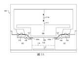
圖1A根據本發明的一些實施例顯示用於電鍍晶圓109之電鍍設備100之垂直橫剖面的通用圖。在一示例實施例中,本文使用的術語晶圓意指半導體晶圓。此外,在各種實施例中,本文指稱的晶圓可在形式、形狀、及/或尺寸上有所不同。舉例而言,在一些實施例中,本文指稱的晶圓可對應於200 mm(毫米)的半導體晶圓、300 mm的半導體晶圓、或450 mm的半導體晶圓。FIG. 1A shows a general view of a vertical cross-section of anelectroplating apparatus 100 for electroplating awafer 109 according to some embodiments of the present invention. In an example embodiment, the term wafer used herein means a semiconductor wafer. In addition, in various embodiments, the wafers referred to herein may differ in form, shape, and/or size. For example, in some embodiments, the wafer referred to herein may correspond to a 200 mm (millimeter) semiconductor wafer, a 300 mm semiconductor wafer, or a 450 mm semiconductor wafer.

電鍍設備100包含杯構件101及錐狀構件103。電鍍設備100亦包含唇封構件105,該唇封構件105係配置成嚙合杯構件101的頂部。若干指狀接觸件107係在唇封構件105的頂部上加以配置。指狀接觸件107係以圓形構造加以配置,以針對待處理的晶圓109之周緣區域提供實質均勻支撐。Theelectroplating apparatus 100 includes acup member 101 and atapered member 103. Theelectroplating apparatus 100 also includes alip seal member 105 configured to engage the top of thecup member 101. A number offinger contacts 107 are arranged on the top of thelip seal member 105. Thefinger contacts 107 are arranged in a circular configuration to provide substantially uniform support for the peripheral area of thewafer 109 to be processed.

圖2A根據本發明的一些實施例顯示指狀接觸件107的頂視圖。圖2B根據本發明的一些實施例顯示通過該等指狀接觸件107其中一者之如圖2A所示之「A-A剖面」的垂直橫剖面圖。如圖2A所示,該若干指狀接觸件107係與環形導電條107A(例如金屬條)連接而整體形成。指狀接觸件107及導電條107A兩者皆係導電的。應理解在各種實施例中,指狀接觸件107及導電條107A可由任何導電材料形成,該導電材料針對電鍍製程的執行提供足夠的電傳導,且該導電材料具有足夠的機械特性以在電鍍製程期間支撐晶圓109,且該導電材料係與在電鍍製程期間所曝露的環境及材料化學相容。Figure 2A shows a top view of afinger contact 107 according to some embodiments of the invention. 2B shows a vertical cross-sectional view of the "A-A section" shown in FIG. 2A through one of thefinger contacts 107 according to some embodiments of the present invention. As shown in FIG. 2A, the plurality of finger-shapedcontacts 107 are connected to the ring-shapedconductive strip 107A (for example, a metal strip) to be integrally formed. Both thefinger contact 107 and theconductive strip 107A are conductive. It should be understood that in various embodiments, thefinger contacts 107 and theconductive strips 107A may be formed of any conductive material that provides sufficient electrical conduction for the execution of the electroplating process, and the conductive material has sufficient mechanical properties to be used in the electroplating process. Thewafer 109 is supported during the process, and the conductive material is chemically compatible with the environment and material exposed during the electroplating process.

如圖2B及1A所示,指狀接觸件107係形狀設計成沿唇封構件105之頂部的上部輪廓向下彎曲。而且,相對於導電條107A的周向構造,指狀接觸件107的內端部段107B係向上轉以提供晶圓109的支撐表面107C。更具體而言,在電鍍製程期間,晶圓109係位在指狀接觸件107的支撐表面107C上,其中待電鍍之晶圓109的表面朝下,以物理接觸指狀接觸件107的支撐表面107C。As shown in FIGS. 2B and 1A, thefinger contact 107 is shaped to be curved downward along the upper contour of the top of thelip seal member 105. Moreover, with respect to the circumferential configuration of theconductive strip 107A, theinner end section 107B of thefinger contact 107 is turned upward to provide a supportingsurface 107C of thewafer 109. More specifically, during the electroplating process, thewafer 109 is positioned on thesupport surface 107C of thefinger contact 107, wherein the surface of thewafer 109 to be electroplated faces downward to physically contact the support surface of thefinger contact 107 107C.

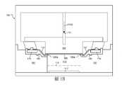
錐狀構件103係附接至軸111,該軸111係配置成相對於杯構件101上下移動,如箭頭111A所示。在電鍍製程期間,錐狀構件103係向下移動以與晶圓109介接及將晶圓109按壓在指狀接觸件107的支撐表面107C之上,以使指狀接觸件107的內端部段107B朝唇封構件105向下撓曲,以便抵著唇封構件105的密封表面105A按壓晶圓109的周緣向下區域。圖1B根據本發明的一些實施例顯示圖1A之錐狀構件103向下移動(如箭頭111B所示),以與晶圓109介接以便抵著唇封構件105的密封表面105A按壓晶圓109之周緣向下區域的圖。The taperedmember 103 is attached to theshaft 111, which is configured to move up and down relative to thecup member 101, as indicated by thearrow 111A. During the electroplating process, the taperedmember 103 moves downward to interface with thewafer 109 and press thewafer 109 on the supportingsurface 107C of thefinger contact 107, so that the inner end of thefinger contact 107 Thesection 107B flexes downward toward thelip seal member 105 so as to press the downward peripheral edge of thewafer 109 against the sealingsurface 105A of thelip seal member 105. FIG. 1B shows that the taperedmember 103 of FIG. 1A moves downward (as indicated by thearrow 111B) to interface with thewafer 109 so as to press thewafer 109 against the sealingsurface 105A of thelip seal member 105 according to some embodiments of the present invention. A diagram of the downward area of the periphery.

杯構件101的內部區域形成用於容納電鍍溶液的槽容積113。當晶圓109係藉由錐狀構件103施加之向下的力抵著唇封構件105的密封表面105A而加以按壓時,密封部係在晶圓109與密封表面105A之間加以形成,使得電鍍溶液不會超出晶圓109與唇封構件105的密封表面105A之間的接觸位置,從而使電鍍溶液遠離指狀接觸件107。The inner area of thecup member 101 forms atank volume 113 for containing the electroplating solution. When thewafer 109 is pressed against the sealingsurface 105A of thelip seal member 105 by the downward force exerted by the taperedmember 103, the sealing portion is formed between thewafer 109 and the sealingsurface 105A, so that electroplating The solution does not exceed the contact position between thewafer 109 and the sealingsurface 105A of thelip seal member 105, thereby keeping the electroplating solution away from thefinger contact 107.

電鍍設備100亦包含配置成物理接觸導電條107A的匯流排(bus bar)115,從而在匯流排115與指狀接觸件107之間建立電連接。匯流排係由固體金屬片形成,用於改善圍繞晶圓109之周緣的方位角電鍍均勻性。Theelectroplating equipment 100 also includes abus bar 115 configured to physically contact theconductive bar 107A, thereby establishing an electrical connection between thebus bar 115 and thefinger contact 107. The bus bar is formed of a solid metal sheet to improve the uniformity of the azimuth angle plating around the periphery of thewafer 109.

槽容積113包含陽極構件117。在一些實施例中,陽極構件117係由銅形成。然而,在其他實施例中,陽極構件117可由適合正在執行之特定電鍍製程的其它導電材料形成。在一些實施例中,膜118係配置在槽容積113之內,以將在膜118下方的陽極區域與在膜118上方的陰極區域物理分隔。膜118係配置成當允許陽極區域與陰極區域之間的離子連通時,避免在陽極區域與陰極區域之間之電解液(電鍍溶液)的主體連通。在一些實施例中,膜118係離子選擇性膜。Thetank volume 113 contains theanode member 117. In some embodiments, theanode member 117 is formed of copper. However, in other embodiments, theanode member 117 may be formed of other conductive materials suitable for the particular electroplating process being performed. In some embodiments, themembrane 118 is disposed within thecell volume 113 to physically separate the anode region below themembrane 118 from the cathode region above themembrane 118. Themembrane 118 is configured to prevent the main body of the electrolyte (plating solution) from communicating between the anode area and the cathode area when ions between the anode area and the cathode area are allowed to communicate. In some embodiments, themembrane 118 is an ion selective membrane.

在電鍍製程期間,直流電源的正極端子係電連接至陽極構件117,且直流電源的負極端子係電連接至匯流排115。以此方式,電流流徑係自陽極構件117經過電鍍溶液至曝露於電鍍溶液之晶圓109的表面,及從晶圓109的表面至指狀接觸件107,及從指狀接觸件107至匯流排115而加以建立。通常,在電鍍製程之前,導電晶種層係在待鍍覆之晶圓109的表面上加以形成,從而在整個晶圓109提供初始的電導性。然後,當材料在電鍍製程期間在晶圓109上加以沉積/生長時,沉積的材料有助於整個晶圓109的電導性。During the electroplating process, the positive terminal of the DC power source is electrically connected to theanode member 117, and the negative terminal of the DC power source is electrically connected to thebus bar 115. In this way, the current flow path is from theanode member 117 through the electroplating solution to the surface of thewafer 109 exposed to the electroplating solution, and from the surface of thewafer 109 to thefinger contact 107, and from thefinger contact 107 to the sink. Row 115 to be established. Generally, before the electroplating process, a conductive seed layer is formed on the surface of thewafer 109 to be plated, so as to provide initial electrical conductivity throughout thewafer 109. Then, when the material is deposited/grown on thewafer 109 during the electroplating process, the deposited material contributes to the electrical conductivity of theentire wafer 109.

在許多電鍍製程循環期間,一些電鍍溶液可能侵入通過在晶圓109與唇封構件105的密封表面105A之間的接觸位置,且到達指狀接觸件107。當此發生時,某些材料可能被電鍍在指狀接觸件107之上及/或在唇封構件105之上。當材料係被電鍍在指狀接觸件107之上及/或在唇封構件105之上時,那些電鍍之指狀接觸件107及/或唇封構件105之電鍍部分的電特性將加以改變,使得在晶圓109上在由電鍍之指狀接觸件107及/或唇封構件105之電鍍部分之改變的電特性所電性影響的位置處造成不利的電鍍結果。舉例而言,晶圓109上之不利的電鍍結果可表現為較薄之電鍍材料厚度的區域,其從而導致整個晶圓109的電鍍不均勻性,其從而可能導致半導體裝置製造的難度及/或缺陷。During many electroplating process cycles, some electroplating solution may intrude through the contact position between thewafer 109 and the sealingsurface 105A of thelip seal member 105 and reach thefinger contact 107. When this happens, certain materials may be electroplated on thefinger contacts 107 and/or on thelip seal member 105. When the material is electroplated on thefinger contacts 107 and/or on thelip seal member 105, the electrical characteristics of theelectroplated finger contacts 107 and/or the electroplated part of thelip seal member 105 will be changed. This causes adverse electroplating results on thewafer 109 at positions that are electrically affected by the changed electrical characteristics of theelectroplated finger contacts 107 and/or the electroplated portion of thelip seal member 105. For example, the unfavorable electroplating results on thewafer 109 may be manifested in areas of thinner electroplating material thickness, which may lead to uneven electroplating of theentire wafer 109, which may lead to difficulties in the manufacture of semiconductor devices and/or defect.

圖3A根據本發明的示例實施例顯示電鍍厚度及指狀接觸件107之電阻隨著沿晶圓109之給定半徑的方位角變化的示例圖,其中所有指狀接觸件107具有可接受的電阻。電鍍厚度係以微米為單位呈現。指狀接觸件107之電阻係以毫歐姆為單位呈現。方位角係繞垂直於晶圓109的頂表面及底表面延伸且通過晶圓109之中心點之晶圓109的中心軸而加以測量。如圖3A所示,在具有良好狀態之指狀接觸件107的情況下,材料的電鍍厚度沿晶圓109的給定半徑係實質上均勻,其係期望的電鍍結果。FIG. 3A shows an example diagram of the plating thickness and the resistance of thefinger contact 107 with the azimuth angle along a given radius of thewafer 109 according to an exemplary embodiment of the present invention, wherein all thefinger contacts 107 have acceptable resistance . The plating thickness is expressed in micrometers. The resistance of thefinger contact 107 is expressed in milliohms. The azimuth angle is measured around the center axis of thewafer 109 that extends perpendicular to the top and bottom surfaces of thewafer 109 and passes through the center point of thewafer 109. As shown in FIG. 3A, in the case offinger contacts 107 in good condition, the plating thickness of the material is substantially uniform along a given radius of thewafer 109, which is a desired plating result.

圖3B根據本發明的示例實施例顯示兩個晶圓109獲得之電鍍厚度的圖,一個晶圓109使用所有狀態良好的指狀接觸件107,而另一晶圓109使用狀態不佳的一些指狀接觸件107。圖3B的電鍍厚度圖顯示為隨著沿兩個晶圓109之給定半徑的方位角之函數。狀態不佳的指狀接觸件107,由於電鍍溶液洩漏經過在晶圓109與唇封構件105的密封表面105A之間的接觸位置,而經歷不期望的電鍍。因為在狀態不佳的指狀接觸件107上的電鍍導致一些變色,所以這些狀態不佳的指狀接觸件107係稱為變色的接觸件及具有在可接受規格之外的電特性,例如電阻。如圖3B所示,基於電鍍厚度中的偏差(aberration),變色的指狀接觸件107看起來像位在約130度和約188度的方位角之間。3B shows a graph of the plating thickness obtained for twowafers 109 according to an exemplary embodiment of the present invention. Onewafer 109 uses all thefinger contacts 107 in good condition, and theother wafer 109 uses some fingers in poor condition.状contact 107. The electroplating thickness graph of FIG. 3B is shown as a function of the azimuth angle along a given radius of the twowafers 109. Thefinger contact 107 in poor condition undergoes undesirable electroplating due to the leakage of the electroplating solution through the contact position between thewafer 109 and the sealingsurface 105A of thelip seal member 105. Because the electroplating on thefinger contacts 107 in poor condition causes some discoloration, thesefinger contacts 107 in poor condition are called discolored contacts and have electrical characteristics outside acceptable specifications, such as electrical resistance. . As shown in FIG. 3B, based on the aberration in the plating thickness, thediscolored finger contact 107 appears to be located between an azimuth angle of about 130 degrees and about 188 degrees.

圖3C根據本發明的示例實施例顯示:使用一些變色的指狀接觸件107進行電鍍之晶圓109之電鍍厚度在一給定半徑隨方位角變化的圖(如圖3B所示),以及針對該電鍍使用之指狀接觸件107之電阻隨方位角變化的圖。圖3C顯示在電鍍厚度係不均勻的方位角位置,相應之變色的指狀接觸件107相對於其他指狀接觸件107具有高電阻,其表示在變色的指狀接觸件107上材料的不期望電鍍。Fig. 3C shows a graph of the electroplating thickness of awafer 109 electroplated with somediscolored finger contacts 107 with a given radius as a function of the azimuth angle according to an exemplary embodiment of the present invention (as shown in Fig. 3B), and A graph of the resistance of thefinger contact 107 used in this electroplating as a function of the azimuth angle. Figure 3C shows that at the azimuthal position where the plating thickness is uneven, the corresponding discoloredfinger contact 107 has a high resistance relative toother finger contacts 107, which indicates that the material on thediscolored finger contact 107 is undesirable plating.

鑑於上述情況,應理解從電鍍厚度及均勻性來看,維持可接受的電鍍結果係取決於維持指狀接觸件107及唇封構件105的良好狀態。而且,為了維持指狀接觸件107及唇封構件105的良好狀態,需要監視在指狀接觸件107及/或唇封構件105上的電鍍是否發生且發生到怎樣的程度。此外,此監測應以不顯著影響電鍍設備100之可用性的方式加以進行。In view of the above, it should be understood that from the point of view of plating thickness and uniformity, maintaining an acceptable plating result depends on maintaining the good condition of thefinger contacts 107 and thelip seal member 105. Furthermore, in order to maintain the good state of thefinger contacts 107 and thelip seal member 105, it is necessary to monitor whether and to what extent the plating on thefinger contacts 107 and/or thelip seal member 105 has occurred. In addition, this monitoring should be performed in a way that does not significantly affect the usability of theelectroplating equipment 100.

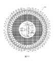
圖4A根據本發明的一些實施例顯示裝置400(測量裝置400)的頂視圖,該裝置400用於測量在電鍍設備100中之指狀接觸件107及唇封構件105的電性狀態。裝置400包含具有類似於晶圓109之形態因子(form factor)的印刷電路板。因此,裝置400可以與晶圓109相同的方式加以搬運,且可以與晶圓109相同的方式在電鍍設備100之內加以配置。此外,裝置400可像任何晶圓一樣使用在製造設施中的任何晶圓輸送設備加以移動。另外,裝置400可如任何晶圓加以儲存。在一些實施例中,裝置400係在電鍍工具的伴隨晶圓插槽中加以儲存,且係藉由晶圓輸送機器人在電鍍設備100中加以配置,以藉由裝置400提供指狀接觸件107及/或唇封構件105之電特性的測量。然而,應理解在一些實施例中,裝置400可手工在電鍍設備100中加以配置,以藉由裝置400提供指狀接觸件107及/或唇封構件105之電特性的測量。FIG. 4A shows a top view of a device 400 (a measuring device 400) according to some embodiments of the present invention. Thedevice 400 is used to measure the electrical state of thefinger contact 107 and thelip seal member 105 in theelectroplating equipment 100. Thedevice 400 includes a printed circuit board with a form factor similar to that of thewafer 109. Therefore, theapparatus 400 can be transported in the same manner as thewafer 109, and can be arranged in theelectroplating apparatus 100 in the same manner as thewafer 109. In addition, theapparatus 400 can be moved using any wafer transport equipment in a manufacturing facility like any wafer. In addition, thedevice 400 can be stored like any wafer. In some embodiments, thedevice 400 is stored in the accompanying wafer slot of the electroplating tool, and is configured in theelectroplating apparatus 100 by a wafer transfer robot, so that thedevice 400 provides thefinger contacts 107 and / Or measurement of the electrical characteristics of thelip seal member 105. However, it should be understood that in some embodiments, thedevice 400 may be manually configured in theelectroplating apparatus 100 to provide the measurement of the electrical characteristics of thefinger contact 107 and/or thelip seal member 105 by thedevice 400.

裝置400包含多個露出之導電的墊401,該等導電的墊係沿裝置400的外部徑向區域加以配置。每個相鄰之一對導電的墊401係藉由隔離構件403(例如電絕緣體材料)彼此電分離。每個導電的墊401包含至電源405的電連接件404及至測量電路407的電連接件406。在一些實施例中,電源405可配置成經由導電路徑提供受控量的電流,該導電路徑係在電源405的第一端子405A與電源405的第二端子405B之間延伸。在一些實施例中,電源405係配置成在電源405的第一端子405A與電源405的第二端子405B之間供應受控量的電壓。所有導電的墊401之電連接件404係通過開關電路409至電源405,使得電流及/或電壓在一給定時間可提供至該等導電的墊401之任何一者以上。而且,所有導電的墊401之電連接件406係通過開關電路409至測量電路407,使得存在該等導電的墊401之任何一者以上的電參數可在一給定時間加以測量。在一些實施例中,測量電路407包含類比數位轉換電路,用於將測量的類比電參數轉換為數位格式。測量電路407亦包含記憶體模組413,用於以數位格式儲存測量的電參數。Thedevice 400 includes a plurality of exposedconductive pads 401, and the conductive pads are arranged along the outer radial area of thedevice 400. Each adjacent pair ofconductive pads 401 is electrically separated from each other by an isolation member 403 (for example, an electrical insulator material). Eachconductive pad 401 includes anelectrical connection 404 to thepower source 405 and anelectrical connection 406 to themeasurement circuit 407. In some embodiments, thepower source 405 may be configured to provide a controlled amount of current via a conductive path that extends between thefirst terminal 405A of thepower source 405 and the second terminal 405B of thepower source 405. In some embodiments, thepower source 405 is configured to supply a controlled amount of voltage between thefirst terminal 405A of thepower source 405 and the second terminal 405B of thepower source 405. Theelectrical connections 404 of allconductive pads 401 are connected to thepower supply 405 through theswitch circuit 409, so that current and/or voltage can be provided to any one of theconductive pads 401 at a given time. Moreover, all theelectrical connections 406 of theconductive pads 401 pass through theswitch circuit 409 to themeasurement circuit 407, so that the electrical parameters of any one or more of theconductive pads 401 can be measured at a given time. In some embodiments, themeasurement circuit 407 includes an analog-to-digital conversion circuit for converting the measured analog electrical parameters into a digital format. Themeasurement circuit 407 also includes amemory module 413 for storing the measured electrical parameters in a digital format.

電源405、測量電路407及開關電路409的每一者係配置成在控制模組411的指示下加以操作。以此方式,在一給定時間,控制模組411係加以操作以指揮開關電路409,以將該等導電的墊401之特定一者以上連接至電源405,及將該等導電的墊401之特定一者以上連接至測量電路407。此外,電源405、測量電路407及開關電路409的每一者係加以連接,以從電源供應器415接收電功率。在一些實施例中,電源供應器415是電池。在一些實施例中,電源供應器415是充電電池。Each of thepower supply 405, themeasurement circuit 407, and theswitch circuit 409 is configured to be operated under the instruction of thecontrol module 411. In this way, at a given time, thecontrol module 411 is operated to command theswitch circuit 409 to connect more than one of theconductive pads 401 to thepower source 405, and to connect theconductive pads 401 to thepower source 405. One or more specific ones are connected to themeasurement circuit 407. In addition, each of thepower supply 405, themeasurement circuit 407, and theswitch circuit 409 are connected to receive electric power from thepower supply 415. In some embodiments, thepower supply 415 is a battery. In some embodiments, thepower supply 415 is a rechargeable battery.

此外,裝置400包含通訊模組417,該通訊模組417係配置成傳送對應於由測量電路407測量的電參數之數位資料及/或對應於裝置400之條件的數位資料。在一些實施例中,通訊模組417係配置成將數位資料無線傳輸至在裝置400之範圍內的無線接收器。而且,在一些實施例中,通訊模組417係配置成支持至裝置400的有線連接,數位資料可經由該有線連接加以傳輸。而且,在一些實施例中,通訊模組417係配置成支持無線通訊模式及有線通訊模式兩者。通訊模組417係加以連接,以從電源供應器415接收電功率。因此,在通訊模組417係配置成支持無線通訊模式的情況下,裝置400係能夠以完全自主及獨立的方式加以操作,使得裝置400可以與晶圓109相同的方式移動通過製造設施及通過電鍍工具。In addition, thedevice 400 includes acommunication module 417 configured to transmit digital data corresponding to the electrical parameters measured by the measuringcircuit 407 and/or digital data corresponding to the conditions of thedevice 400. In some embodiments, thecommunication module 417 is configured to wirelessly transmit digital data to a wireless receiver within the range of thedevice 400. Moreover, in some embodiments, thecommunication module 417 is configured to support a wired connection to thedevice 400 through which digital data can be transmitted. Moreover, in some embodiments, thecommunication module 417 is configured to support both a wireless communication mode and a wired communication mode. Thecommunication module 417 is connected to receive electric power from thepower supply 415. Therefore, when thecommunication module 417 is configured to support the wireless communication mode, thedevice 400 can be operated in a completely autonomous and independent manner, so that thedevice 400 can move through the manufacturing facility and through electroplating in the same manner as thewafer 109 tool.

此外,控制模組411可藉由通訊模組417加以編程,以使用電源405及測量電路407指揮任何規定形式之測量的執行。因此,應理解控制模組411係加以連接,以將控制訊號傳送至通訊模組417、電源405、測量電路407、記憶體模組413、電源供應器415及開關電路409的每一者,以及自通訊模組417、電源405、測量電路407、記憶體模組413、電源供應器415及開關電路409的每一者接收資料訊號。In addition, thecontrol module 411 can be programmed by thecommunication module 417 to use thepower supply 405 and themeasurement circuit 407 to command the execution of any prescribed form of measurement. Therefore, it should be understood that thecontrol module 411 is connected to transmit control signals to each of thecommunication module 417, thepower supply 405, themeasurement circuit 407, thememory module 413, thepower supply 415, and theswitch circuit 409, and The data signal is received from each of thecommunication module 417, thepower supply 405, themeasurement circuit 407, thememory module 413, thepower supply 415, and theswitch circuit 409.

圖4B根據本發明的一些實施例顯示來自圖4A的裝置400,其中開關電路409係更詳細地加以顯示。應理解,圖4B之特定的開關電路409之配置係作為示例加以提供。在其他實施例中,開關電路409可配置成與圖4B之示例中顯示的開關電路不同。更具體而言,在其他實施例中,開關電路409可實質上以任何方式加以配置,只要存在以下功能:在一給定時間將選擇的一個以上導電的墊401電連接至電源405,及在該給定時間將選擇的一個以上導電的墊401電連接至測量電路407。此外,應理解本文關於裝置400顯示或描述的任何電連接性,可實質上使用電跡線的任何適當配置在裝置400的印刷電路板內/上加以實現。而且,在一些實施例中,裝置400的印刷電路板可包含多層電跡線,其中相鄰的電跡線層藉由介電材料彼此隔開,且依需要具有用以連接不同層中之電跡線的通孔導體。FIG. 4B shows thedevice 400 from FIG. 4A according to some embodiments of the present invention, in which theswitch circuit 409 is shown in more detail. It should be understood that the configuration of thespecific switch circuit 409 of FIG. 4B is provided as an example. In other embodiments, theswitch circuit 409 may be configured to be different from the switch circuit shown in the example of FIG. 4B. More specifically, in other embodiments, theswitch circuit 409 can be configured in essentially any manner, as long as there is the following function: electrically connect the selected one or moreconductive pads 401 to thepower source 405 at a given time, and The selected one or moreconductive pads 401 are electrically connected to themeasurement circuit 407 at the given time. In addition, it should be understood that any electrical connectivity shown or described herein with respect to thedevice 400 can be implemented in/on the printed circuit board of thedevice 400 using essentially any suitable configuration of electrical traces. Moreover, in some embodiments, the printed circuit board of thedevice 400 may include multiple layers of electrical traces, wherein adjacent electrical trace layers are separated from each other by a dielectric material, and have electrical connections for connecting different layers as required. The through-hole conductor of the trace.

在圖4B之開關電路409的配置中,每個電連接件404從相應之導電的墊401延伸至相應的電流開關模組419。而且,每個電連接件406從相應之導電的墊401延伸至相應的測量開關模組421。因此,每個導電的墊401具有對應的電流開關模組419及對應的測量開關模組421。In the configuration of theswitch circuit 409 in FIG. 4B, eachelectrical connector 404 extends from the correspondingconductive pad 401 to the correspondingcurrent switch module 419. Moreover, eachelectrical connector 406 extends from the correspondingconductive pad 401 to the correspondingmeasurement switch module 421. Therefore, eachconductive pad 401 has a correspondingcurrent switch module 419 and a correspondingmeasurement switch module 421.

電源匯流排423係加以提供,用於與每一電流開關模組419連接。而且,參考接地匯流排425係加以提供,用於與每一電流開關模組419連接。電源匯流排423與參考接地匯流排425兩者係電連接至電源405,使得電源405可加以操作,以在控制模組411的控制下將電流供應至電源匯流排423,且自參考接地匯流排425汲取電流。Apower bus 423 is provided for connection with eachcurrent switch module 419. Furthermore, a reference ground bus 425 is provided for connection with eachcurrent switch module 419. Both thepower bus 423 and the reference ground bus 425 are electrically connected to thepower source 405, so that thepower source 405 can be operated to supply current to thepower bus 423 under the control of thecontrol module 411, and from the reference ground bus 425 draws current.

第一測量匯流排427係加以提供,用於與每一測量開關模組421連接。而且,第二測量匯流排429係加以提供,用於與每一測量開關模組421連接。第一測量匯流排427及第二測量匯流排429兩者係電連接至測量電路407。在控制模組411的控制下,測量電路407可加以操作,以在一給定時間感測在第一測量匯流排427上的電訊號及/或在第二測量匯流排429上的電訊號。Thefirst measurement bus 427 is provided for connection with eachmeasurement switch module 421. Moreover, asecond measurement bus 429 is provided for connection with eachmeasurement switch module 421. Both thefirst measurement bus 427 and thesecond measurement bus 429 are electrically connected to themeasurement circuit 407. Under the control of thecontrol module 411, themeasurement circuit 407 can be operated to sense the electrical signal on thefirst measurement bus 427 and/or the electrical signal on thesecond measurement bus 429 at a given time.

圖5根據本發明的一些實施例顯示一給定導電的墊401之電路圖,其中,該給定導電的墊401之電連接件404連接至其電流開關模組419,且其中,該給定導電的墊401之電連接件406連接至其測量開關模組421。在電流開關模組419之內,電連接件404係連接至一對開關裝置501及503。在一些實施例中,每一開關裝置501及503係被實施為整合電路開關裝置。然而,在一些實施例中,開關裝置501及503可被實施為類比開關裝置。每一開關裝置501及503係在控制模組411的控制下,如分別由連接件505及507所示。開關裝置501具有連接至電源匯流排423的一端子,該電源匯流排423係如前所述又連接至電源405。而且,開關裝置503具有連接至參考接地匯流排425的一端子,該參考接地匯流排425係如前所述又連接至電源405。使用此配置,控制模組411可操作開關裝置501及503,以將導電的墊401電連接至電源匯流排423或參考接地匯流排425。以此方式,依據在電流開關模組419之內之開關裝置501及503的設定,電流及/或電壓可在一給定時間從電源405施加至特定之導電的墊401,或特定之導電的墊401可在該給定時間電連接至參考接地電位。FIG. 5 shows a circuit diagram of a givenconductive pad 401 according to some embodiments of the present invention, wherein theelectrical connector 404 of the givenconductive pad 401 is connected to itscurrent switch module 419, and wherein the givenconductive pad 401 Theelectrical connector 406 of thepad 401 is connected to themeasurement switch module 421 thereof. In thecurrent switch module 419, theelectrical connector 404 is connected to a pair ofswitch devices 501 and 503. In some embodiments, each switchingdevice 501 and 503 is implemented as an integrated circuit switching device. However, in some embodiments, the switchingdevices 501 and 503 may be implemented as analog switching devices. Eachswitch device 501 and 503 is under the control of thecontrol module 411, as shown by theconnectors 505 and 507, respectively. Theswitch device 501 has a terminal connected to thepower bus 423, which is connected to thepower source 405 as described above. Furthermore, theswitching device 503 has a terminal connected to the reference ground bus 425, which is connected to thepower source 405 as described above. With this configuration, thecontrol module 411 can operate theswitching devices 501 and 503 to electrically connect theconductive pad 401 to thepower bus 423 or the reference ground bus 425. In this way, according to the settings of theswitching devices 501 and 503 in thecurrent switch module 419, current and/or voltage can be applied from thepower supply 405 to the specificconductive pad 401 or the specificconductive pad 401 at a given time Thepad 401 may be electrically connected to the reference ground potential at the given time.

在測量開關模組421之內,電連接件406係連接至一對開關裝置509及511。在一些實施例中,每一開關裝置509及511係被實施為整合電路開關裝置。然而,在一些實施例中,開關裝置509及511可被實施為類比開關裝置。每一開關裝置509及511係在控制模組411的控制下,如分別由連接件513及515所示。開關裝置509具有連接至第一測量匯流排427的一端子,該第一測量匯流排427係如前所述又連接至測量電路407。而且,開關裝置511具有連接至第二測量匯流排429的一端子,該第二測量匯流排429係如前所述又連接至測量電路407。使用此配置,控制模組411可操作開關裝置509及511,以將導電的墊401電連接至第一測量匯流排427或第二測量匯流排429。以此方式,依據在測量開關模組421之內之開關裝置509及511的設定,測量電路407可加以連接,以在一給定時間感測在特定之導電的墊401處的高電流及/或電壓,或在該給定時間感測在特定之導電的墊401處的低電流及/或電壓。In themeasurement switch module 421, theelectrical connector 406 is connected to a pair ofswitch devices 509 and 511. In some embodiments, each switchingdevice 509 and 511 is implemented as an integrated circuit switching device. However, in some embodiments, the switchingdevices 509 and 511 may be implemented as analog switching devices. Eachswitch device 509 and 511 is under the control of thecontrol module 411, as shown by theconnectors 513 and 515, respectively. Theswitching device 509 has a terminal connected to the first measuringbus 427, which is connected to the measuringcircuit 407 as described above. Furthermore, theswitching device 511 has a terminal connected to thesecond measuring bus 429, which is connected to the measuringcircuit 407 as described above. With this configuration, thecontrol module 411 can operate theswitching devices 509 and 511 to electrically connect theconductive pad 401 to thefirst measurement bus 427 or thesecond measurement bus 429. In this way, according to the settings of theswitching devices 509 and 511 in the measuringswitch module 421, the measuringcircuit 407 can be connected to sense the high current and/or the high current at the specificconductive pad 401 at a given time. Or the voltage, or sense the low current and/or voltage at the specificconductive pad 401 at the given time.

圖6A根據本發明的一些實施例顯示裝置400的圖,該裝置400係配置成置放在指狀接觸件107的支撐表面107C上。圖6A中描繪的視圖係在從朝錐狀構件103向上看之槽容積113內部的視角。如圖6A所示,導電的墊401接觸指狀接觸件107的支撐表面107C,以在每一導電的墊401及與該導電的墊401物理接觸之指狀接觸件107的對應子集合之間建立導電路徑。以此方式,每一導電的墊401係與指狀接觸件107的不同子集合電連接。FIG. 6A shows a diagram of adevice 400 configured to be placed on the supportingsurface 107C of thefinger contact 107 according to some embodiments of the present invention. The view depicted in FIG. 6A is from the perspective of the inside of thegroove volume 113 viewed upward from the taperedmember 103. As shown in FIG. 6A, theconductive pad 401 contacts the supportingsurface 107C of thefinger contact 107 so as to be between eachconductive pad 401 and the corresponding subset of thefinger contact 107 in physical contact with theconductive pad 401 Establish a conductive path. In this way, eachconductive pad 401 is electrically connected to a different subset offinger contacts 107.

圖6B根據本發明的一些實施例顯示通過裝置400及指狀接觸件107之如圖6A所示之「B-B剖面」的垂直橫剖面圖。如圖6A所示,裝置400係配置成使得導電的墊401置放在指狀接觸件107的支撐表面107C上。正如進行電鍍處理的晶圓109一樣,裝置400可接觸錐狀構件103以使用精確控制量之向下的力將導電的墊401按壓在指狀接觸件107的支撐表面107C上。此外,應理解裝置400的旋轉位置可分度至電鍍設備100,以便知道指狀接觸件107的哪一子集合係與該等導電的墊401之特定一者物理接觸。因為裝置400具有類似於晶圓109之形態因子的形態因子,所以裝置400可使用在電鍍設備100連接之製造工作站可得的標準晶圓對準器裝置旋轉分度至電鍍設備100。FIG. 6B shows a vertical cross-sectional view of the passingdevice 400 and thefinger contact 107 as shown in FIG. 6A in the "B-B section" according to some embodiments of the present invention. As shown in FIG. 6A, thedevice 400 is configured such that theconductive pad 401 is placed on the supportingsurface 107C of thefinger contact 107. Just like thewafer 109 undergoing electroplating, thedevice 400 can contact thetapered member 103 to press theconductive pad 401 against thesupport surface 107C of thefinger contact 107 with a precisely controlled amount of downward force. In addition, it should be understood that the rotational position of thedevice 400 can be indexed to theelectroplating equipment 100 in order to know which subset of thefinger contacts 107 is in physical contact with a specific one of theconductive pads 401. Because thedevice 400 has a form factor similar to the form factor of thewafer 109, thedevice 400 can be rotated and indexed to theelectroplating equipment 100 using a standard wafer aligner device available at the manufacturing workstation to which theelectroplating equipment 100 is connected.

在開關電路409之適當設定的情況下,電流及/或電壓可從電源405通過一給定之導電的墊401,被引導至與該給定之導電的墊物理連接之指狀接觸件107的特定子集合。而且,在開關電路409之適當設定的情況下,與一給定之導電的墊401物理連接之指狀接觸件107的特定子集合可電連接至參考接地電位。以此方式,藉由操作控制模組411及開關電路409,精確控制的電流可加以引導,以在圍繞裝置400之周緣的第一方位位置處流入第一導電的墊401,及通過與該第一導電的墊401物理接觸之指狀接觸件107的第一特定子集合,且自指狀接觸件107的該第一特定子集合通過導電條107A(及可能通過與導電條107A接觸的其他導電元件,諸如匯流排115)至在圍繞裝置400之周緣的第二方位位置處之指狀接觸件107的第二特定子集合,及從指狀接觸件107的該第二特定子集合至在圍繞裝置400之周緣的該第二方位位置處之第二導電的墊401,及自該第二導電的墊401至參考接地電位。而且,類似地,藉由操作控制模組411及開關電路409,精確控制的電壓可在圍繞裝置400之周緣的該第一方位位置處的第一導電的墊401與圍繞裝置400之周緣和該第二方位位置處的第二導電的墊401之間加以施加。When theswitch circuit 409 is properly set, the current and/or voltage can be guided from thepower source 405 through a givenconductive pad 401 to a specific sub-contact of thefinger contact 107 physically connected to the given conductive pad. gather. Moreover, with the proper setting of theswitch circuit 409, a specific subset of thefinger contacts 107 physically connected to a givenconductive pad 401 can be electrically connected to the reference ground potential. In this way, by operating thecontrol module 411 and theswitch circuit 409, a precisely controlled current can be guided to flow into the firstconductive pad 401 at the first azimuth position around the periphery of thedevice 400, and pass through the firstconductive pad 401. A first specific subset of thefinger contacts 107 of aconductive pad 401 in physical contact, and from this first specific subset of thefinger contacts 107 through theconductive strip 107A (and possibly other conductive strips in contact with theconductive strip 107A) Element, such as bus bar 115) to a second specific subset offinger contacts 107 at a second azimuthal position around the periphery ofdevice 400, and from this second specific subset offinger contacts 107 to surrounding The secondconductive pad 401 at the second azimuth position of the periphery of thedevice 400 and from the secondconductive pad 401 to the reference ground potential. Moreover, similarly, by operating thecontrol module 411 and theswitch circuit 409, the voltage can be precisely controlled between the firstconductive pad 401 at the first azimuth position surrounding the periphery of thedevice 400 and the periphery of thedevice 400 and the It is applied between the secondconductive pads 401 at the second azimuth position.

控制模組411可加以編程以指揮開關電路409的操作,以針對第一方位位置選擇該等導電的墊401之任一者,及針對第二方位位置選擇該等導電的墊401之任一者。在一些實施例中,第二方位位置對應於配置在第一導電的墊401旁邊之導電的墊401,其中第一導電的墊401對應於第一方位位置。在一些實施例中,多個導電的墊401係加以選擇,以提供多個第二方位位置。舉例而言,在一些實施例中,多個第二方位位置對應於分別配置在第一導電的墊401之每一側上的兩個導電的墊401。在該特定的示例中,電流將流入第一導電的墊401,且經由毗鄰該第一導電的墊401之兩個導電的墊401兩者返回。Thecontrol module 411 can be programmed to direct the operation of theswitch circuit 409 to select any one of theconductive pads 401 for the first azimuth position and select any one of theconductive pads 401 for the second azimuth position . In some embodiments, the second azimuth position corresponds to theconductive pad 401 disposed beside the firstconductive pad 401, wherein the firstconductive pad 401 corresponds to the first azimuth position. In some embodiments, a plurality ofconductive pads 401 are selected to provide a plurality of second orientation positions. For example, in some embodiments, the plurality of second azimuth positions correspond to twoconductive pads 401 respectively arranged on each side of the firstconductive pad 401. In this particular example, current will flow into the firstconductive pad 401 and return via both of the twoconductive pads 401 adjacent to the firstconductive pad 401.

結合操作裝置400以將精確控制的電流引導流入在第一方位位置處之指狀接觸件107的第一子集合,且在第二方位位置處自指狀接觸件107的第二子集合返回,控制模組411可加以編程以指揮開關電路409,以將測量電路407連接至在第一方位位置處之第一導電的墊401及在第二方位位置處之第二導電的墊401之其中一或二者,從而提供在第一方位位置處之第一導電的墊401及在第二方位位置處之第二導電的墊401之其中一或二者的電壓及/或電流之測量。Combining theoperating device 400 to direct a precisely controlled current into the first subset of thefinger contacts 107 at the first azimuth position, and return from the second subset of thefinger contacts 107 at the second azimuth position, Thecontrol module 411 can be programmed to command theswitch circuit 409 to connect themeasurement circuit 407 to one of the firstconductive pad 401 at the first position and the secondconductive pad 401 at the second position. Or both, so as to provide a measurement of the voltage and/or current of one or both of the firstconductive pad 401 at the first azimuth position and the secondconductive pad 401 at the second azimuth position.

當製造裝置400時,在裝置400之內之導電路徑(例如跡線)的電阻係仔細地加以測量。因此,當精確控制的電流係流入指狀接觸件107的第一子集合且自指狀接觸件107的第二子集合返回時,沿在指狀接觸件107的第一子集合與指狀接觸件107的第二子集合之間的導電路徑之電阻,可加以測量且與一允許的電阻範圍相比,以判定不良電鍍是否沿在指狀接觸件107的第一子集合與指狀接觸件107的第二子集合之間的導電路徑發生。以此方式,裝置400可加以操作,以測量在繞裝置400整個周緣之指狀接觸件107之不同子集合之間的電阻,以充分描繪整體指狀接觸件107之電阻的特性,及識別不良電鍍是否已在指狀接觸件107之特定者上發生。When manufacturingdevice 400, the resistance of conductive paths (eg, traces) withindevice 400 is carefully measured. Therefore, when the precisely controlled current flows into the first subset of thefinger contacts 107 and returns from the second subset of thefinger contacts 107, the first subset of thefinger contacts 107 is in contact with the fingers. The resistance of the conductive path between the second subset of theelement 107 can be measured and compared with an allowable resistance range to determine whether the poor plating is along the first subset of thefinger contact 107 and the finger contact. The conductive path between the second subset of 107 occurs. In this way, thedevice 400 can be operated to measure the electrical resistance between different subsets of thefinger contacts 107 around the entire periphery of thedevice 400, so as to fully characterize the electrical resistance of theoverall finger contacts 107 and identify poorly. Whether electroplating has occurred on a specific one of thefinger contacts 107.

圖7根據本發明的一些實施例顯示一電路圖,該電路圖表示電源405的連接方式以將電流供應至第一導電的墊401A,及表示第二導電的墊401B的連接方式,以汲取電流返回至電源405。電源405係配置成在第一端子405A供應電流且在第二端子405B汲取電流。電源405係加以連接以經由電連接件701將電流供應至第一導電的墊401A。如先前關於圖5所述,電連接件701係經由開關電路409佈線至第一導電的墊401A。沿電連接件701的電阻711係加以測量且已知。電源405係加以連接以經由電連接件703自第二導電的墊401B汲取電流。如先前關於圖5所述,電連接件703係經由開關電路409佈線至第二導電的墊401B。沿電連接件703的電阻713係加以測量且已知。FIG. 7 shows a circuit diagram according to some embodiments of the present invention. The circuit diagram shows the connection method of thepower supply 405 to supply current to the firstconductive pad 401A and the connection method of the secondconductive pad 401B to draw current back toPower supply 405. Thepower supply 405 is configured to supply current at thefirst terminal 405A and draw current at thesecond terminal 405B. Thepower supply 405 is connected to supply current to the firstconductive pad 401A via theelectrical connection 701. As previously described with respect to FIG. 5, theelectrical connection 701 is wired to the firstconductive pad 401A via theswitch circuit 409. Theresistance 711 along theelectrical connection 701 is measured and known. Thepower supply 405 is connected to draw current from the secondconductive pad 401B via theelectrical connection 703. As previously described with respect to FIG. 5, theelectrical connection 703 is wired to the secondconductive pad 401B via theswitch circuit 409. Theresistance 713 along theelectrical connection 703 is measured and known.

圖7亦顯示與第一導電的墊401A電連接之指狀接觸件107的第一子集合107-1,及與第二導電的墊401B電連接之指狀接觸件107的第二子集合107-2。在指狀接觸件107之第一子集合107-1中的每個指狀接觸件107,係經由導電條107A電連接至在指狀接觸件107之第二子集合107-2中的每個指狀接觸件107。沿在指狀接觸件107的第一子集合107-1與指狀接觸件107之第二子集合107-2之間之導電條107A部分的電阻709,係加以測量且已知。此外,導電條107A係與匯流排115電連接。沿在指狀接觸件107的第一子集合107-1與指狀接觸件107之第二子集合107-2之間之匯流排115部分的電阻715,係加以測量且已知。此外,導電條107A係與唇封構件105電連接。由於在唇封構件105上可能具有電鍍的材料,所以沿在指狀接觸件107的第一子集合107-1與指狀接觸件107之第二子集合107-2之間之唇封構件105部分的電阻717係未知的。FIG. 7 also shows a first subset 107-1 offinger contacts 107 electrically connected to the firstconductive pad 401A, and asecond subset 107 offinger contacts 107 electrically connected to the secondconductive pad 401B -2. Eachfinger contact 107 in the first subset 107-1 of thefinger contact 107 is electrically connected to each of the second subset 107-2 of thefinger contact 107 via aconductive strip107A Finger contact 107. Theresistance 709 along the portion of theconductive strip 107A between the first subset 107-1 of thefinger contacts 107 and the second subset 107-2 of thefinger contacts 107 is measured and known. In addition, thebus bar 107A is electrically connected to thebus bar 115. Theresistance 715 along the portion of thebus 115 between the first subset 107-1 of thefinger contacts 107 and the second subset 107-2 of thefinger contacts 107 is measured and known. In addition, thebus bar 107A is electrically connected to thelip seal member 105. Since there may be electroplated material on thelip seal member 105, along thelip seal member 105 between the first subset 107-1 of thefinger contact 107 and the second subset 107-2 of thefinger contact 107 Part of theresistance 717 is unknown.

測量電路407係加以連接,以經由佈線至測量電路407之第一輸入端子407A的電連接件705測量存在第一導電的墊401A上的電特性,例如電流及/或電壓。如先前關於圖5所述,電連接件705係經由開關電路409佈線至第一導電的墊401A。沿電連接件705的電阻719係加以測量且已知。測量電路407係亦加以連接,以經由佈線至測量電路407之第二輸入端子407B的電連接件707測量存在第二導電的墊401B上的電特性,例如電流及/或電壓。如先前關於圖5所述,電連接件707係經由開關電路409佈線至第二導電的墊401B。沿電連接件707的電阻721係加以測量且已知。The measuringcircuit 407 is connected to measure the electrical characteristics of the firstconductive pad 401A, such as current and/or voltage, via theelectrical connection 705 wired to thefirst input terminal 407A of the measuringcircuit 407. As previously described with respect to FIG. 5, theelectrical connection 705 is wired to the firstconductive pad 401A via theswitch circuit 409. Theresistance 719 along theelectrical connection 705 is measured and known. Themeasurement circuit 407 is also connected to measure the electrical characteristics, such as current and/or voltage, on the secondconductive pad 401B through theelectrical connection 707 wired to thesecond input terminal 407B of themeasurement circuit 407. As previously described with respect to FIG. 5, theelectrical connection 707 is wired to the secondconductive pad 401B via theswitch circuit 409. Theresistance 721 along theelectrical connection 707 is measured and known.

在電源405與第一導電的墊401A和第二導電的墊401B之每一者之間的各種電阻及其他電特性係已知的。而且,在測量電路407與第一導電的墊401A和第二導電的墊401B之每一者之間的各種電阻及其他電特性係已知的。此外,沿在指狀接觸件107之第一子集合107-1與指狀接觸件107之第二子集合107-2之間的導電條107A之電阻及其他電特性係已知的。此外,沿在指狀接觸件107之第一子集合107-1與指狀接觸件107之第二子集合107-2之間的匯流排115之電阻及其他電特性係已知的。因此,在圖7的電路中,由於在指狀接觸件107上及/或在唇封構件105上存在之電鍍材料的可能性,所以整體的電阻(經由指狀接觸件107之第一子集合107-1及指狀接觸件107之第二子集合107-2的各種指狀接觸件107,及經由在指狀接觸件107之第一子集合107-1與指狀接觸件107之第二子集合107-2之間延伸的唇封構件105部分)係未知的。Various resistances and other electrical characteristics between thepower source 405 and each of the firstconductive pad 401A and the secondconductive pad 401B are known. Moreover, various resistances and other electrical characteristics between themeasurement circuit 407 and each of the firstconductive pad 401A and the secondconductive pad 401B are known. In addition, the electrical resistance and other electrical characteristics along theconductive strip 107A between the first subset 107-1 of thefinger contact 107 and the second subset 107-2 of thefinger contact 107 are known. In addition, the electrical resistance and other electrical characteristics along thebus bar 115 between the first subset 107-1 of thefinger contacts 107 and the second subset 107-2 of thefinger contacts 107 are known. Therefore, in the circuit of FIG. 7, due to the possibility of electroplating material on thefinger contact 107 and/or on thelip seal member 105, the overall resistance (via the first subset of the finger contact 107) 107-1 andvarious finger contacts 107 of the second subset 107-2 of thefinger contacts 107, and through the first subset 107-1 of thefinger contacts 107 and the second subset of thefinger contacts 107 The portion of thelip seal member 105 extending between the subset 107-2) is unknown.

藉由將精確控制的電流施加至第一導電的墊401A及藉由汲取來自第二導電的墊401B之施加的電流,及結合操作測量電路407以測量在第一導電的墊401A和第二導電的墊401B之每一者的電壓及/或電流,上述整體的電阻可加以測量及評估,以判定不良電鍍是否在指狀接觸件107的第一子集合107-1及/或指狀接觸件107的第二子集合107-2之內發生,及/或不良電鍍是否經由在指狀接觸件107的第一子集合107-1與指狀接觸件107的第二子集合107-2之間延伸的唇封構件105部份發生。在一些實施例中,測量電路407包含由電源供應器415結合電源405供電的分路電阻器,以沿電鍍設備100之選擇的方位段測量通過指狀接觸件107及唇封構件105的電阻。應理解裝置400提供沿電鍍設備100之任何選擇的方位段之指狀接觸件107及唇封構件105之電阻的測量。By applying a precisely controlled current to the firstconductive pad 401A and by drawing the applied current from the secondconductive pad 401B, and operating the measuringcircuit 407 to measure the firstconductive pad 401A and the secondconductive pad 401A The voltage and/or current of each of thepads 401B, the above-mentioned overall resistance can be measured and evaluated to determine whether poor plating is in the first subset 107-1 of thefinger contact 107 and/or thefinger contact 107 occurs within the second subset 107-2 of 107, and/or whether poor plating occurs between the first subset 107-1 of thefinger contact 107 and the second subset 107-2 of thefinger contact 107 The extendedlip seal member 105 occurs partially. In some embodiments, themeasurement circuit 407 includes a shunt resistor powered by thepower supply 415 in combination with thepower supply 405 to measure the resistance through thefinger contact 107 and thelip seal member 105 along the selected azimuth section of theelectroplating apparatus 100. It should be understood that thedevice 400 provides a measurement of the electrical resistance of thefinger contacts 107 and thelip seal member 105 along any selected azimuth section of theelectroplating apparatus 100.

藉由監控指狀接觸件107及唇封構件105的電特性,在指狀接觸件107及/或唇封構件105的狀態指示產生不良電鍍結果之可能性的情況下,針對電鍍設備100的維修發出警報是可能的。此外,在一些實施例中,諸如光學感測器的額外感測器可在裝置400之內加以實現,以提供指狀接觸件107群及唇封構件105之相應方位段的目視觀察。By monitoring the electrical characteristics of thefinger contacts 107 and thelip seal member 105, when the state of thefinger contacts 107 and/or thelip seal member 105 indicates the possibility of poor electroplating results, the maintenance of theelectroplating equipment 100 It is possible to issue an alarm. In addition, in some embodiments, additional sensors such as optical sensors may be implemented within thedevice 400 to provide visual observation of the corresponding orientation segments of thefinger contact 107 group and thelip seal member 105.

在一些實施例中,裝置400係在電鍍工具上的伴隨晶圓插槽中加以儲存,且係被排程為用機器人移動至進行測量的電鍍設備100,所以不需要使用者互動。一旦完成測量,裝置400係返回至伴隨晶圓插槽,在此時,裝置400將測量數據傳送至電鍍工具以進行記錄及分析。此外,在指狀接觸件107之電阻及唇封構件105之功能中的趨勢可隨元件老化加以記錄。In some embodiments, thedevice 400 is stored in a companion wafer slot on the electroplating tool and is scheduled to be moved by a robot to theelectroplating equipment 100 for measurement, so no user interaction is required. Once the measurement is completed, thedevice 400 returns to the companion wafer slot. At this time, thedevice 400 transmits the measurement data to the electroplating tool for recording and analysis. In addition, trends in the electrical resistance of thefinger contact 107 and the function of thelip seal member 105 can be recorded as the component ages.

鑑於上述情況,應理解本文揭示的裝置400提供測量在電鍍設備(諸如電鍍設備100)之內之電接觸件的電特性,其中該電鍍設備係配置成在晶圓109上執行電鍍製程。然而,亦應理解通常本文揭示的裝置400可用於測量在半導體處理設備(其可能是或可能不是電鍍設備)之內之導電路徑的電特性,其中該半導體處理設備係配置成當在晶圓109上執行製程時,將導電路徑電連接至晶圓109的表面。裝置400包含盤狀結構,該盤狀結構的外徑實質上等於晶圓109的外徑。在一些實施例中,裝置400的盤狀結構係印刷電路板。裝置400之盤狀結構的整體厚度實質上類似於晶圓109的整體厚度。In view of the foregoing, it should be understood that theapparatus 400 disclosed herein provides for measuring the electrical characteristics of electrical contacts within an electroplating apparatus (such as the electroplating apparatus 100) that is configured to perform an electroplating process on thewafer 109. However, it should also be understood that generally thedevice 400 disclosed herein can be used to measure the electrical characteristics of conductive paths within a semiconductor processing device (which may or may not be an electroplating device), where the semiconductor processing device is configured to act as awafer 109 When performing the process, the conductive path is electrically connected to the surface of thewafer 109. Thedevice 400 includes a disk-shaped structure, and the outer diameter of the disk-shaped structure is substantially equal to the outer diameter of thewafer 109. In some embodiments, the disc-like structure of thedevice 400 is a printed circuit board. The overall thickness of the disc-shaped structure of thedevice 400 is substantially similar to the overall thickness of thewafer 109.

裝置400包含多個導電的墊401,該等導電的墊401係沿盤狀結構之第一側的外周緣加以形成。該多個導電的墊401之相鄰配置者係彼此電隔離。在一些實施例中,裝置400的盤狀結構係由電絕緣材料形成,且該多個導電的墊401之相鄰配置者係藉由盤狀結構的一部分彼此隔離,從而提供在該多個導電的墊401之相鄰配置者之間的電隔離。在一些實施例中,電隔離結構(諸如隔離構件403)係在盤狀結構上加以配置,以將該多個導電的墊401之相鄰配置者彼此電隔離。該多個導電的墊401共同界定盤狀結構之第一側的外周緣。在一些實施例中,多個導電的墊401之每一者的尺寸係與沿裝置400之盤狀結構之第一側的外周緣測量的尺寸實質相等。Thedevice 400 includes a plurality ofconductive pads 401 formed along the outer periphery of the first side of the disc-shaped structure. Adjacent configurations of the plurality ofconductive pads 401 are electrically isolated from each other. In some embodiments, the disc-shaped structure of thedevice 400 is formed of an electrically insulating material, and the adjacent dispositions of the plurality ofconductive pads 401 are isolated from each other by a part of the disc-shaped structure, thereby providing the plurality of conductive pads. Thepad 401 is electrically isolated between adjacent ones. In some embodiments, an electrical isolation structure (such as the isolation member 403) is configured on the disk-shaped structure to electrically isolate adjacent configurations of the plurality ofconductive pads 401 from each other. The plurality ofconductive pads 401 jointly define the outer periphery of the first side of the disc-shaped structure. In some embodiments, the size of each of the plurality ofconductive pads 401 is substantially the same as the size measured along the outer periphery of the first side of the disc-shaped structure of thedevice 400.

裝置400包含具有第一端子405A及第二端子405B的電源405。當裝置400的盤狀結構係配置在半導體處理設備之內時,電源405係配置成經由在第一端子405A和第二端子405B之間延伸的導電路徑及經由半導體處理設備的一部分供應電功率。第一端子405A係電連接至多個導電的墊401之其中至少一者的第一集合。第二端子405B係電連接至多個導電的墊401之其中至少一者的第二集合。該多個導電的墊401之該第二集合係不包括該多個導電的墊401之該第一集合。該多個導電的墊401之該第一及第二集合形成在第一端子405A及第二端子405B之間延伸之導電路徑的一部分。在一些實施例中,電源係配置成經由在第一端子405A及第二端子405B之間延伸的導電路徑供應受控量的電流。在一些實施例中,電源係配置成在第一端子405A及第二端子405B之間供應受控量的電壓。Thedevice 400 includes apower supply 405 having afirst terminal 405A and asecond terminal 405B. When the disc-shaped structure of thedevice 400 is configured within the semiconductor processing equipment, thepower supply 405 is configured to supply electric power via a conductive path extending between thefirst terminal 405A and thesecond terminal 405B and through a part of the semiconductor processing equipment. Thefirst terminal 405A is electrically connected to a first set of at least one of the plurality ofconductive pads 401. Thesecond terminal 405B is electrically connected to a second set of at least one of the plurality ofconductive pads 401. The second set of the plurality ofconductive pads 401 does not include the first set of the plurality ofconductive pads 401. The first and second sets of the plurality ofconductive pads 401 form part of the conductive path extending between thefirst terminal 405A and thesecond terminal 405B. In some embodiments, the power supply is configured to supply a controlled amount of current via a conductive path extending between thefirst terminal 405A and thesecond terminal 405B. In some embodiments, the power supply is configured to supply a controlled amount of voltage between thefirst terminal 405A and thesecond terminal 405B.

裝置400亦包含具有第一輸入端子407A及第二輸入端子407B的測量電路407。測量電路407的第一輸入端子407A係電連接至多個導電的墊401之選擇的第一者。測量電路407的第二輸入端子407B係電連接至多個導電的墊401之選擇的第二者。測量電路407係配置成基於在該多個導電的墊401之該選擇的第一及第二者處存在的電訊號,判定電參數的值。在一些實施例中,測量電路407係配置成基於在該多個導電的墊401之該選擇的第一及第二者處存在的電訊號,測量電壓及電流其中一或二者。在一些實施例中,測量電路407係配置成基於在第一輸入端子407A存在的第一測量訊號及在第二輸入端子407B存在的第二測量訊號測量電壓。在一些實施例中,測量電路407係配置成,基於在第一輸入端子407A存在的第一測量訊號及在第二輸入端子407B存在的第二測量訊號測量電流。Thedevice 400 also includes ameasurement circuit 407 having afirst input terminal 407A and asecond input terminal 407B. Thefirst input terminal 407A of themeasurement circuit 407 is electrically connected to the first selected one of the plurality ofconductive pads 401. Thesecond input terminal 407B of themeasurement circuit 407 is electrically connected to the selected second one of the plurality ofconductive pads 401. The measuringcircuit 407 is configured to determine the value of the electrical parameter based on the electrical signal existing at the selected first and second ones of the plurality ofconductive pads 401. In some embodiments, themeasurement circuit 407 is configured to measure one or both of voltage and current based on electrical signals present at the selected first and second ones of the plurality ofconductive pads 401. In some embodiments, themeasurement circuit 407 is configured to measure the voltage based on the first measurement signal present at thefirst input terminal 407A and the second measurement signal present at thesecond input terminal 407B. In some embodiments, themeasurement circuit 407 is configured to measure the current based on the first measurement signal present at thefirst input terminal 407A and the second measurement signal present at thesecond input terminal 407B.

裝置400包含開關電路409,該開關電路409係配置成,在一給定時間將電源405的第一端子405A連接至多個導電的墊401之選擇的第一者。開關電路409係亦配置成,在該給定時間將電源405的第二端子405B連接至多個導電的墊401之選擇的第二者。開關電路409係亦配置成,在該給定時間將測量電路407的第一輸入端子407A連接至該多個導電的墊401之該選擇的第一者。而且,開關電路409係配置成,在該給定時間將測量電路407的第二輸入端子407B連接至該多個導電的墊401之該選擇的第二者。裝置400亦包含在盤狀結構上配置的電源供應器415。電源供應器415係加以連接,以將電功率供應至在盤狀結構上之裝置400的所有電動元件。在一些實施例中,電源供應器415係電池。Thedevice 400 includes aswitch circuit 409 configured to connect thefirst terminal 405A of thepower source 405 to a selected first of the plurality ofconductive pads 401 at a given time. Theswitch circuit 409 is also configured to connect the second terminal 405B of thepower source 405 to a selected second one of the plurality ofconductive pads 401 at the given time. Theswitch circuit 409 is also configured to connect thefirst input terminal 407A of themeasurement circuit 407 to the selected first one of the plurality ofconductive pads 401 at the given time. Furthermore, theswitch circuit 409 is configured to connect thesecond input terminal 407B of themeasurement circuit 407 to the selected second one of the plurality ofconductive pads 401 at the given time. Thedevice 400 also includes apower supply 415 arranged on a disc-shaped structure. Thepower supply 415 is connected to supply electric power to all the electric components of thedevice 400 on the disc structure. In some embodiments, thepower supply 415 is a battery.

在一些實施例中,裝置400包含在盤狀結構上配置的控制模組411。控制模組411係配置成指揮電源405及測量電路407及開關電路409的操作。在一些實施例中,控制模組411係配置成指揮開關電路409,以在一給定時間將多個導電的墊401之其中特定一者以上連接至電源405的第一端子405A。而且,在一些實施例中,控制模組411係配置成指揮開關電路409,以在該給定時間將多個導電的墊401之其中特定一者以上連接至電源405的第二端子405B。在一些實施例中,開關電路409係加以操作以確保,在該給定時間電連接至電源405之第二端子405B之多個導電的墊401的其中該一者以上,係不同於在該給定時間電連接至電源405之第一端子405A之多個導電的墊401之其中該一者以上,以避免在電源405的第一端子405A及第二端子405B之間的電短路。In some embodiments, thedevice 400 includes acontrol module 411 configured on a disc-shaped structure. Thecontrol module 411 is configured to direct the operation of thepower supply 405, themeasurement circuit 407, and theswitch circuit 409. In some embodiments, thecontrol module 411 is configured to direct theswitch circuit 409 to connect a specific one of the plurality ofconductive pads 401 to thefirst terminal 405A of thepower source 405 at a given time. Moreover, in some embodiments, thecontrol module 411 is configured to direct theswitch circuit 409 to connect a specific one of the plurality ofconductive pads 401 to the second terminal 405B of thepower source 405 at the given time. In some embodiments, theswitch circuit 409 is operated to ensure that more than one of theconductive pads 401 electrically connected to the second terminal 405B of thepower source 405 at the given time is different from that in the More than one of theconductive pads 401 electrically connected to thefirst terminal 405A of thepower source 405 at a fixed time to avoid electrical short circuit between thefirst terminal 405A and the second terminal 405B of thepower source 405.

在一些實施例中,開關電路409係配置成,在一給定時間將多個導電的墊401之其中任何兩者以上選擇性地電連接至測量電路407的第一輸入端子407A。此外,在一些實施例中,開關電路409係配置成,在該給定時間將多個導電的墊401之其中任何兩者以上選擇性地電連接至測量電路407的第二輸入端子407B。在一些實施例中,開關電路409係加以操作以確保,在該給定時間電連接至測量電路407之第二輸入端子407B之多個導電的墊401的其中該兩者以上,係不同於在該給定時間電連接至測量電路407之第一輸入端子407A之多個導電的墊401之其中該兩者以上。In some embodiments, theswitch circuit 409 is configured to selectively electrically connect any two or more of the plurality ofconductive pads 401 to thefirst input terminal 407A of themeasurement circuit 407 at a given time. In addition, in some embodiments, theswitch circuit 409 is configured to selectively electrically connect any two or more of the plurality ofconductive pads 401 to thesecond input terminal 407B of themeasurement circuit 407 at the given time. In some embodiments, theswitch circuit 409 is operated to ensure that more than two of theconductive pads 401 electrically connected to thesecond input terminal 407B of themeasurement circuit 407 at the given time are different from those in the The predetermined time is electrically connected to more than two of theconductive pads 401 of thefirst input terminal 407A of themeasurement circuit 407.

在一些實施例中,裝置400係配置成具有記憶體模組413,該記憶體模組413係定義為在盤狀結構上的電腦記憶體。該電腦記憶體係配置成儲存表示由測量電路407判定之電參數的值之數位資料。此外,在一些實施例中,測量電路407包含類比數位轉換電路,用於將電參數的值轉換為表示電參數的值之數位資料。此外,在一些實施例中,裝置400係配置成包含在盤狀結構上配置的通訊模組417。在一些實施例中,通訊模組417係配置成無線地傳送表示由測量電路407判定之電參數的值之資料。In some embodiments, thedevice 400 is configured to have amemory module 413, which is defined as a computer memory on a disk-like structure. The computer memory system is configured to store digital data representing the value of the electrical parameter determined by themeasurement circuit 407. In addition, in some embodiments, themeasurement circuit 407 includes an analog-digital conversion circuit for converting the value of the electrical parameter into digital data representing the value of the electrical parameter. In addition, in some embodiments, thedevice 400 is configured to include acommunication module 417 arranged on a disc-shaped structure. In some embodiments, thecommunication module 417 is configured to wirelessly transmit data representing the value of the electrical parameter determined by themeasurement circuit 407.

在一些實施例中,配置在裝置400之盤狀結構上的控制模組411係配置成指揮電源405、測量電路407、開關電路409、電源供應器415、記憶體模組413及通訊模組417的操作。在一些實施例中,控制模組411係配置成指揮開關電路409,以在該給定時間將多個導電的墊401之其中特定一者以上連接至電源405的第一端子405A,及在該給定時間將多個導電的墊401之其中特定一者以上連接至電源405的第二端子405B,及在該給定時間將多個導電的墊401之其中特定一者以上連接至測量電路407的第一輸入端子407A,及在該給定時間將多個導電的墊401之其中特定一者以上連接至測量電路407的第二輸入端子407B。In some embodiments, thecontrol module 411 configured on the disc structure of thedevice 400 is configured as acommand power supply 405, ameasurement circuit 407, aswitch circuit 409, apower supply 415, amemory module 413, and acommunication module 417 Operation. In some embodiments, thecontrol module 411 is configured to direct theswitch circuit 409 to connect more than one specific one of the plurality ofconductive pads 401 to thefirst terminal 405A of thepower source 405 at the given time, and in the Connect specific one or more of the plurality ofconductive pads 401 to the second terminal 405B of thepower supply 405 at a given time, and connect specific one or more of the plurality ofconductive pads 401 to themeasurement circuit 407 at the given time Thefirst input terminal 407A is connected to thesecond input terminal 407B of themeasurement circuit 407 at the given time.

圖8根據本發明的一些實施例顯示一種方法的流程圖,該方法用於測量在半導體處理設備(諸如電鍍設備100等)之內之導電路徑的電特性。半導體處理設備係配置成當在晶圓109上執行製程時,將導電路徑電連接至晶圓109的表面。該方法包含操作801,用於將測量裝置400配置在半導體處理設備之內。測量裝置400具有一盤狀結構,其中該盤狀結構的外徑與晶圓109的外徑實質相等,且其中該盤狀結構的整體厚度實質上類似於晶圓109的整體厚度。測量裝置400係配置在半導體處理設備之內,使得沿測量裝置400之第一側的外周緣形成之多個導電的墊401物理接觸在半導體處理設備之內的電接觸件107。多個導電的墊401之相鄰配置者係在測量裝置400上彼此電隔離。而且,該多個導電的墊401共同界定測量裝置400之第一側的外周緣。FIG. 8 shows a flowchart of a method according to some embodiments of the present invention for measuring the electrical characteristics of conductive paths within a semiconductor processing device (such as theelectroplating device 100, etc.). The semiconductor processing equipment is configured to electrically connect the conductive path to the surface of thewafer 109 when the process is performed on thewafer 109. The method includesoperation 801 for configuring themeasurement device 400 in a semiconductor processing device. The measuringdevice 400 has a disc-shaped structure, wherein the outer diameter of the disc-shaped structure is substantially equal to the outer diameter of thewafer 109, and the overall thickness of the disc-shaped structure is substantially similar to the overall thickness of thewafer 109. The measuringdevice 400 is disposed in the semiconductor processing equipment, so that the plurality ofconductive pads 401 formed along the outer periphery of the first side of the measuringdevice 400 physically contact theelectrical contacts 107 in the semiconductor processing equipment. The adjacent configurations of the plurality ofconductive pads 401 are electrically isolated from each other on themeasuring device 400. Moreover, the plurality ofconductive pads 401 jointly define the outer periphery of the first side of the measuringdevice 400.

該方法亦包含操作803,用於操作測量裝置400以經由導電路徑供應電功率,該導電路徑包含多個導電的墊401之其中至少一者的第一集合及多個導電的墊401之其中至少一者的第二集合,其中該多個導電的墊401之該第二集合係不包括該多個導電的墊401之該第一集合。該方法亦包含操作805,用於操作測量裝置400,以測量在該多個導電的墊401之選擇的第一者處及在該多個導電的墊401之選擇的第二者處存在的電訊號。The method also includesoperation 803 for operating the measuringdevice 400 to supply electric power via a conductive path including a first set of at least one of a plurality ofconductive pads 401 and at least one of a plurality ofconductive pads 401 The second set of the plurality ofconductive pads 401 does not include the first set of the plurality ofconductive pads 401. The method also includesoperation 805 for operating the measuringdevice 400 to measure the telecommunications existing at the selected first of the plurality ofconductive pads 401 and at the selected second of the plurality ofconductive pads 401 No.

該方法亦包含操作807,用於操作測量裝置400,以使用測量的電訊號判定導電路徑的特徵參數,該導電路徑延伸穿過半導體處理設備的一部分,且包含該多個導電的墊401之該選擇的第一者及該多個導電的墊401之該選擇的第二者。該方法亦可包含操作測量裝置400,以傳送(以無線及/或有線的方式)及/或儲存表示導電路徑之特徵參數的值之資料。The method also includesoperation 807 for operating the measuringdevice 400 to determine the characteristic parameter of the conductive path using the measured electrical signal. The conductive path extends through a part of the semiconductor processing equipment and includes the plurality ofconductive pads 401. The selected first and the selected second of the plurality ofconductive pads 401. The method may also include operating the measuringdevice 400 to transmit (in a wireless and/or wired manner) and/or store data representing the value of the characteristic parameter of the conductive path.

在一些實施例中,延伸穿過半導體處理設備之該部分的導電路徑之特徵參數是電阻值。舉例而言,在電鍍設備100的實施例中,當測量裝置400係配置在半導體處理設備(電鍍設備100)之內時,在半導體處理設備(電鍍設備100)之內的導電路徑可包含與多個導電的墊401物理接觸的電接觸件107。更具體而言,該電阻值包含與該多個導電的墊401之該選擇的第一者物理接觸之電接觸件107的電阻,及與該多個導電的墊401之該選擇的第二者物理接觸之電接觸件107的電阻。而且,電阻值可包含通過一段唇封構件105的電阻,該唇封構件105從該多個導電的墊401之該選擇的第一者延伸至該多個導電的墊401之該選擇的第二者。此外,電阻值可包含通過一段匯流排115的電阻,該匯流排115從該多個導電的墊401之該選擇的第一者延伸至該多個導電的墊401之該選擇的第二者。此外,電阻值可包含通過一段導電條107A的電阻,該導電條107A從該多個導電的墊401之該選擇的第一者延伸至該多個導電的墊401之該選擇的第二者。In some embodiments, the characteristic parameter of the conductive path extending through the portion of the semiconductor processing equipment is the resistance value. For example, in the embodiment of theelectroplating equipment 100, when the measuringdevice 400 is disposed in the semiconductor processing equipment (the electroplating equipment 100), the conductive path within the semiconductor processing equipment (the electroplating equipment 100) may include more than one conductive path. Aconductive pad 401 is in physical contact with theelectrical contact 107. More specifically, the resistance value includes the resistance of theelectrical contact 107 that is in physical contact with the selected first of the plurality ofconductive pads 401, and the resistance of the selected second of the plurality ofconductive pads 401 The electrical resistance of theelectrical contact 107 in physical contact. Moreover, the resistance value may include the resistance through a section of thelip seal member 105 that extends from the selected first of the plurality ofconductive pads 401 to the selected second of the plurality ofconductive pads 401 By. In addition, the resistance value may include the resistance through a section of thebus bar 115 that extends from the selected first of the plurality ofconductive pads 401 to the selected second of the plurality ofconductive pads 401. In addition, the resistance value may include the resistance through a section ofconductive strip 107A extending from the selected first of the plurality ofconductive pads 401 to the selected second of the plurality ofconductive pads 401.

在一些實施例中,用於操作測量裝置400以經由導電路徑供應電功率的操作803,包含將電流傳輸通過多個導電的墊401之其中至少一者的第一集合及多個導電的墊401之其中至少一者的第二集合。應理解在各種實施例中,該方法可包含操作測量裝置400,以在一給定時間將電流供應至多個導電的墊401之複數者,或在一給定時間自多個導電的墊401之複數者汲取電流,或以下兩者:在一給定時間將電流供應至多個導電的墊401之複數者及在該給定時間自多個導電的墊401之不同的複數者汲取電流。此外,在一些實施例中,用於操作測量裝置400以通過導電路徑供應電功率的操作803,包含在多個導電的墊401之其中至少一者的第一集合與多個導電的墊401之其中至少一者的第二集合之間施加電壓差。In some embodiments, theoperation 803 for operating the measuringdevice 400 to supply electric power via the conductive path includes transmitting current through a first set of at least one of the plurality ofconductive pads 401 and one of the plurality ofconductive pads 401 The second set of at least one of them. It should be understood that in various embodiments, the method may include operating the measuringdevice 400 to supply current to a plurality of the plurality ofconductive pads 401 at a given time, or from among the plurality ofconductive pads 401 at a given time. A plurality of people draw current, or both: supply current to a plurality ofconductive pads 401 at a given time and draw current from a different plurality ofconductive pads 401 at the given time. In addition, in some embodiments, theoperation 803 for operating the measuringdevice 400 to supply electric power through the conductive path is included in the first set of at least one of the plurality ofconductive pads 401 and among the plurality ofconductive pads 401 A voltage difference is applied between at least one of the second sets.

此外,鑑於上述情況,應理解本文揭示一種系統,該系統用於測量在半導體處理設備(諸如電鍍設備100等)之內之導電路徑的電特性,其中該半導體處理設備係配置成當在晶圓109上執行製程時,將導電路徑電連接至晶圓109的表面。該系統包含測量裝置400,該測量裝置400具有一盤狀結構,其中該盤狀結構的外徑與晶圓109的外徑實質相等,且其中該盤狀結構的整體厚度實質上類似於晶圓109的整體厚度。測量裝置400包含多個導電的墊401,該多個導電的墊401係沿該盤狀結構之第一側的外周緣加以形成。多個導電的墊401之相鄰配置者係彼此電隔離。而且,該多個導電的墊401共同界定該盤狀結構之第一側的外周緣。In addition, in view of the above situation, it should be understood that this document discloses a system for measuring the electrical characteristics of conductive paths in semiconductor processing equipment (such aselectroplating equipment 100, etc.), where the semiconductor processing equipment is configured to act as a wafer When the process is performed on the 109, the conductive path is electrically connected to the surface of thewafer 109. The system includes ameasuring device 400 having a disc-shaped structure, wherein the outer diameter of the disc-shaped structure is substantially equal to the outer diameter of thewafer 109, and the overall thickness of the disc-shaped structure is substantially similar to that of the wafer The overall thickness of 109. The measuringdevice 400 includes a plurality ofconductive pads 401 formed along the outer periphery of the first side of the disc-shaped structure. The adjacent configurations of the plurality ofconductive pads 401 are electrically isolated from each other. Moreover, the plurality ofconductive pads 401 jointly define the outer periphery of the first side of the disc-shaped structure.

測量裝置400包含具有第一端子405A及第二端子405B的電源405。當測量裝置400係配置在半導體處理設備之內時,電源405係配置成經由在第一端子405A和第二端子405B之間延伸的導電路徑及經由半導體處理設備的一部分供應電功率。第一端子405A係電連接至多個導電的墊401之其中至少一者的第一集合。第二端子405B係電連接至多個導電的墊401之其中至少一者的第二集合。該多個導電的墊401之該第二集合係不包括該多個導電的墊401之該第一集合。該多個導電的墊401之該第一及第二集合形成在第一端子405A及第二端子405B之間延伸之導電路徑的一部分。測量裝置400包含具有第一輸入端子407A及第二輸入端子407B的測量電路407。測量電路407的第一輸入端子407A係電連接至多個導電的墊401之選擇的第一者。測量電路407的第二輸入端子407B係電連接至多個導電的墊401之選擇的第二者。測量電路407係配置成基於在該多個導電的墊401之該選擇的第一及第二者處存在的電訊號,判定電參數的值。The measuringdevice 400 includes apower supply 405 having afirst terminal 405A and asecond terminal 405B. When the measuringdevice 400 is configured within the semiconductor processing equipment, thepower supply 405 is configured to supply electric power via a conductive path extending between thefirst terminal 405A and thesecond terminal 405B and through a part of the semiconductor processing equipment. Thefirst terminal 405A is electrically connected to a first set of at least one of the plurality ofconductive pads 401. Thesecond terminal 405B is electrically connected to a second set of at least one of the plurality ofconductive pads 401. The second set of the plurality ofconductive pads 401 does not include the first set of the plurality ofconductive pads 401. The first and second sets of the plurality ofconductive pads 401 form part of the conductive path extending between thefirst terminal 405A and thesecond terminal 405B. The measuringdevice 400 includes a measuringcircuit 407 having afirst input terminal 407A and asecond input terminal 407B. Thefirst input terminal 407A of themeasurement circuit 407 is electrically connected to the first selected one of the plurality ofconductive pads 401. Thesecond input terminal 407B of themeasurement circuit 407 is electrically connected to the selected second one of the plurality ofconductive pads 401. The measuringcircuit 407 is configured to determine the value of the electrical parameter based on the electrical signal existing at the selected first and second ones of the plurality ofconductive pads 401.

測量裝置400包含開關電路409,該開關電路409係配置成,在一給定時間將電源405的第一端子405A連接至多個導電的墊401之其中至少一者的第一集合。開關電路409係配置成,在該給定時間將電源405的第二端子405B連接至多個導電的墊401之其中至少一者的第二集合。開關電路409係配置成,在該給定時間將測量電路407的第一輸入端子407A連接至該多個導電的墊401之該選擇的第一者。而且,開關電路409係配置成,在該給定時間將測量電路407的第二輸入端子407B連接至該多個導電的墊401之該選擇的第二者。The measuringdevice 400 includes aswitch circuit 409 configured to connect thefirst terminal 405A of thepower source 405 to a first set of at least one of the plurality ofconductive pads 401 at a given time. Theswitch circuit 409 is configured to connect the second terminal 405B of thepower source 405 to the second set of at least one of the plurality ofconductive pads 401 at the given time. Theswitch circuit 409 is configured to connect thefirst input terminal 407A of themeasurement circuit 407 to the selected first of the plurality ofconductive pads 401 at the given time. Furthermore, theswitch circuit 409 is configured to connect thesecond input terminal 407B of themeasurement circuit 407 to the selected second one of the plurality ofconductive pads 401 at the given time.

測量裝置400亦包含通訊模組417,該通訊模組417係配置成傳送(以無線及/或有線的方式)表示由測量電路407判定之電參數的值之資料。測量裝置400亦包含電源供應器415,該電源供應器415係加以連接,以將電功率供應至在測量裝置400上的所有電動元件。此外,該系統包含與電鍍設備100相關聯的電腦系統。該電腦系統係配置成自測量裝置400的通訊模組417接收所傳送的資料。此外,測量裝置400可包含資料儲存裝置(諸如記憶體模組413),該資料儲存裝置係配置成儲存基於在該多個導電的墊401之該選擇的第一及第二者處存在的電訊號所判定之電參數的值。Themeasurement device 400 also includes acommunication module 417 configured to transmit (in a wireless and/or wired manner) data representing the value of the electrical parameter determined by themeasurement circuit 407. The measuringdevice 400 also includes apower supply 415 which is connected to supply electric power to all the electrical components on themeasuring device 400. In addition, the system includes a computer system associated with theelectroplating equipment 100. The computer system is configured to receive the transmitted data from thecommunication module 417 of the measuringdevice 400. In addition, the measuringdevice 400 may include a data storage device (such as a memory module 413) configured to store telecommunications existing at the first and second ones based on the selection of the plurality ofconductive pads 401 The value of the electrical parameter determined by the number.

圖9根據本發明的一些實施例顯示一種方法的流程圖,該方法用於操作電鍍設備100以實現自動化電鍍槽評估。該方法包含操作901,用於在新的晶圓109上開始電鍍製程。自操作901,該方法繼續進行操作903,以將晶圓109裝載進電鍍設備100。自操作903,該方法繼續進行操作905,以在晶圓109上執行電鍍製程。自操作905,該方法繼續進行操作907,以自電鍍設備100移除晶圓109。在自電鍍設備100移除晶圓109的操作907之後,決定操作909係加以執行以判定測量製程是否在指狀接觸件107上加以執行。若不執行測量製程,則該方法返回至操作901以在新的晶圓109上開始電鍍製程。FIG. 9 shows a flowchart of a method for operating theelectroplating apparatus 100 to realize automated electroplating tank evaluation according to some embodiments of the present invention. The method includesoperation 901 for starting an electroplating process on anew wafer 109. Sinceoperation 901, the method continues tooperation 903 to load thewafer 109 into theelectroplating apparatus 100. Sinceoperation 903, the method continues tooperation 905 to perform an electroplating process on thewafer 109. Fromoperation 905, the method continues tooperation 907 to remove thewafer 109 from theelectroplating apparatus 100. After theoperation 907 of removing thewafer 109 from theelectroplating apparatus 100, adecision operation 909 is performed to determine whether the measurement process is performed on thefinger contact 107. If the measurement process is not performed, the method returns tooperation 901 to start the electroplating process on thenew wafer 109.

若測量製程係在指狀接觸件107上加以執行,則該方法自操作909繼續進行操作911,用於喚醒測量裝置400。自操作911,該方法繼續進行操作913,用於在方位上對準測量裝置400。測量裝置400的方位對準可在標準晶圓對準器裝置內加以執行。自操作913,該方法繼續進行操作915,用於將測量裝置400移進電鍍設備100,使得測量裝置400係加以配置以使導電的墊401物理接觸指狀接觸件107。自操作915,該方法繼續進行操作917,其中測量裝置400係加以操作,以執行指狀接觸件107及/或唇封構件105之電參數的測量。If the measurement process is performed on thefinger contact 107, the method proceeds fromoperation 909 tooperation 911 to wake up themeasurement device 400. Sinceoperation 911, the method continues tooperation 913 for aligning themeasurement device 400 in an orientation. The orientation alignment of the measuringdevice 400 can be performed in a standard wafer aligner device. Fromoperation 913, the method continues tooperation 915 for moving the measuringdevice 400 into theelectroplating apparatus 100 so that the measuringdevice 400 is configured so that theconductive pad 401 physically contacts thefinger contact 107. Fromoperation 915, the method continues tooperation 917, in which themeasuring device 400 is operated to perform the measurement of the electrical parameters of thefinger contact 107 and/or thelip seal member 105.

自操作917,該方法繼續進行操作919以潤洗測量裝置400。接著,操作921係加以執行,以將測量裝置400返回至其儲存位置。在該儲存位置,測量裝置400的電源供應器415可依需要加以再充電。在一些實施例中,電源供應器415係配置成接收感應充電,使得不需要外部接觸件對電源供應器415充電。然而,在一些實施例中,測量裝置400係配備外部接觸件,用於連接在儲存位置的電源以提供電源供應器415的充電。Sinceoperation 917, the method continues tooperation 919 to rinse themeasuring device 400. Then,operation 921 is performed to return themeasuring device 400 to its storage position. In this storage position, thepower supply 415 of the measuringdevice 400 can be recharged as needed. In some embodiments, thepower supply 415 is configured to receive inductive charging, so that no external contact is required to charge thepower supply 415. However, in some embodiments, the measuringdevice 400 is equipped with external contacts for connecting to the power supply in the storage location to provide thepower supply 415 for charging.

一旦測量裝置400係返回至其儲存位置,該方法繼續進行操作923,以將由測量裝置400獲得的測量資料傳送至與電鍍設備100相關聯的電腦系統。該方法包含操作925,以判定由測量裝置400測量的電參數資料是否係在可接受的限度之內。若電參數資料係判定在可接受的限度之內,則該方法返回至操作901以在新的晶圓109上開始電鍍製程。若電參數資料係判定不在可接受的限度之內,則該方法繼續進行操作927,以開始採取一些補救行動以調整電鍍設備100。在一些實施例中,操作927可包含用於關閉電鍍設備100的操作927A。而且,在一些實施例中,操作927可包含操作927B,用於在製造設備之內發出警報或以其他方式警告操作者電鍍設備100的不良狀況。Once the measuringdevice 400 is returned to its storage location, the method proceeds to operation 923 to transmit the measurement data obtained by the measuringdevice 400 to the computer system associated with theelectroplating equipment 100. The method includesoperation 925 to determine whether the electrical parameter data measured by the measuringdevice 400 is within acceptable limits. If the electrical parameter data is determined to be within the acceptable limit, the method returns tooperation 901 to start the electroplating process on thenew wafer 109. If the electrical parameter data is determined to be not within the acceptable limit, the method proceeds tooperation 927 to begin to take some remedial actions to adjust theelectroplating equipment 100. In some embodiments,operation 927 may includeoperation 927A for shutting down theelectroplating apparatus 100. Moreover, in some embodiments,operation 927 may includeoperation 927B for issuing an alarm within the manufacturing facility or otherwise warning the operator of the bad condition of theelectroplating equipment 100.

圖10根據本發明的一些實施例顯示一種用於評估半導體處理設備狀況之方法的流程圖。該方法包含操作1001,用於以與晶圓109係配置在半導體處理設備之內的相同方式,將測量裝置400配置在半導體處理設備內。半導體處理設備係配置成當在晶圓109上執行製程時,將一條以上導電路徑電連接至晶圓109的表面。測量裝置400具有一盤狀結構,其中該盤狀結構的外徑與晶圓109的外徑實質相等,且其中該盤狀結構的整體厚度實質上類似於晶圓109的整體厚度。測量裝置400係配置在半導體處理設備之內,使得沿測量裝置400之第一側的外周緣形成之多個導電的墊401物理接觸在半導體處理設備之內的電接觸件。該方法亦包含操作1003,用於操作測量裝置400以經由導電路徑供應電功率,該導電路徑包含多個導電的墊之其中至少一者的第一集合及多個導電的墊之其中至少一者的第二集合,其中該多個導電的墊之該第二集合係不包括該多個導電的墊之該第一集合。FIG. 10 shows a flowchart of a method for evaluating the condition of semiconductor processing equipment according to some embodiments of the present invention. The method includesoperation 1001 for arranging the measuringdevice 400 in the semiconductor processing equipment in the same manner as thewafer 109 is arranged in the semiconductor processing equipment. The semiconductor processing equipment is configured to electrically connect more than one conductive path to the surface of thewafer 109 when the process is performed on thewafer 109. The measuringdevice 400 has a disc-shaped structure, wherein the outer diameter of the disc-shaped structure is substantially equal to the outer diameter of thewafer 109, and the overall thickness of the disc-shaped structure is substantially similar to the overall thickness of thewafer 109. The measuringdevice 400 is disposed in the semiconductor processing equipment, so that the plurality ofconductive pads 401 formed along the outer periphery of the first side of the measuringdevice 400 physically contact the electrical contacts in the semiconductor processing equipment. The method also includesoperation 1003 for operating the measuringdevice 400 to supply electric power via a conductive path including a first set of at least one of a plurality of conductive pads and at least one of a plurality of conductive pads A second set, wherein the second set of the plurality of conductive pads does not include the first set of the plurality of conductive pads.

該方法亦包含操作1005,用於操作測量裝置400以測量在多個導電的墊401之選擇的第一者及在多個導電的墊401之選擇的第二者處存在的電訊號,以判定延伸穿過半導體處理設備之一部分之導電路徑的特徵參數。該方法亦包含操作1007,用於從半導體處理設備移除測量裝置400。The method also includesoperation 1005 for operating the measuringdevice 400 to measure the electrical signals present at the first selected one of the plurality ofconductive pads 401 and the second selected second of the plurality ofconductive pads 401 to determine A characteristic parameter of a conductive path that extends through a portion of a semiconductor processing device. The method also includes anoperation 1007 for removing the measuringdevice 400 from the semiconductor processing equipment.

圖10的方法亦可包含用於判定導電路徑的特徵參數是否為可接受的操作。並且,當判定導電路徑的特徵參數係不可接受時,該方法可包含提供半導體處理設備需要維修之通知的操作。而且,當判定導電路徑的特徵參數係可接受時,該方法可包含繼續半導體處理設備之正常操作的操作。該方法亦可包含將測量裝置400儲放在半導體處理設備。此外,當測量裝置400係儲放在半導體處理設備時,該方法可包含對該測量裝置400充電。The method of FIG. 10 may also include an operation for determining whether the characteristic parameter of the conductive path is acceptable. Moreover, when it is determined that the characteristic parameters of the conductive path are not acceptable, the method may include an operation of providing a notification that the semiconductor processing equipment needs maintenance. Moreover, when it is determined that the characteristic parameters of the conductive path are acceptable, the method may include continuing the normal operation of the semiconductor processing equipment. The method may also include storing the measuringdevice 400 in a semiconductor processing facility. In addition, when the measuringdevice 400 is stored in the semiconductor processing equipment, the method may include charging the measuringdevice 400.

應理解本文揭示的測量裝置400可遠程地及自主地操作,而不需要與測量裝置400的使用者互動。此外,在沒有與使用者互動的情況下,測量裝置400提供電鍍設備100元件的監控及測量資料的傳送。而且,本文揭示的測量裝置400可以與晶圓相同的方式藉由機器人置放在電鍍設備100內,且可將結果無線地報告回電鍍工具及/或其他控制系統。在使用測量裝置400的情況下,指狀接觸件107及/或唇封構件105之電參數的測量可排程至電鍍設備100的正常操作排程表中。It should be understood that themeasurement device 400 disclosed herein can be operated remotely and autonomously without interaction with the user of themeasurement device 400. In addition, without interacting with the user, the measuringdevice 400 provides monitoring of the components of theelectroplating equipment 100 and transmission of measurement data. Moreover, the measuringdevice 400 disclosed herein can be placed in theelectroplating equipment 100 by a robot in the same manner as a wafer, and can wirelessly report the results back to the electroplating tool and/or other control systems. When the measuringdevice 400 is used, the measurement of the electrical parameters of thefinger contact 107 and/or thelip seal member 105 can be scheduled to the normal operation schedule of theelectroplating equipment 100.

此外,本文揭示的測量裝置400,不需為了經由指狀接觸件107及/或唇封構件105的特定方位區段分析電阻,而將導電條107A或匯流排115電分離成區段。測量裝置400提供在電性上相同電位之獨立元件的電參數之測量。測量裝置400針對電阻測量提供指狀接觸件107及唇封構件105之特定方位區段的選擇。而且,因為測量裝置400不需為了執行測量存在指狀接觸件107及/或唇封構件105之任何給定方位區段處的電阻而拆卸匯流排115或電鍍設備100的任何其他元件,所以不需停止使用電鍍設備100以評估指狀接觸件107及/或唇封構件105的狀況,從而提供電鍍設備100之可用性的改進及相應之製造設施生產率的改進。In addition, the measuringdevice 400 disclosed herein does not need to electrically separate theconductive strip 107A or thebus bar 115 into sections in order to analyze the resistance through the specific orientation section of thefinger contact 107 and/or thelip seal member 105. The measuringdevice 400 provides the measurement of the electrical parameters of independent components of the same electrical potential. The measuringdevice 400 provides selection of specific orientation sections of thefinger contact 107 and thelip seal member 105 for resistance measurement. Moreover, because themeasuring device 400 does not need to disassemble thebus 115 or any other components of theelectroplating equipment 100 in order to perform the measurement of the resistance at any given azimuth section where thefinger contacts 107 and/or thelip seal member 105 exist, it does not It is necessary to stop using theelectroplating equipment 100 to evaluate the condition of thefinger contacts 107 and/or thelip seal member 105, thereby providing an improvement in the usability of theelectroplating equipment 100 and a corresponding improvement in the productivity of the manufacturing facility.

傳統電鍍設備檢查方法依賴目視檢查以識別由於唇封構件105失效引起的嚴重電鍍溶液洩漏之證據,及評估指狀接觸件107的外觀以檢查指狀接觸件107上的電鍍。因此,傳統的檢查方法本質上係定性的。與這些傳統檢查方法相比,應理解本文揭示的測量裝置400提供電鍍槽元件(諸如指狀接觸件107及唇封構件105)之電參數的定量測量。此外,測量裝置400可提供電鍍設備100元件的老化及嚴重失效之監控,其係無法使用傳統檢查方法加以監控。Conventional inspection methods for electroplating equipment rely on visual inspection to identify evidence of serious electroplating solution leakage due to the failure of thelip seal member 105, and to evaluate the appearance of thefinger contact 107 to check the electroplating on thefinger contact 107. Therefore, traditional inspection methods are qualitative in nature. Compared with these conventional inspection methods, it should be understood that the measuringdevice 400 disclosed herein provides a quantitative measurement of electrical parameters of the electroplating bath elements (such as thefinger contacts 107 and the lip seal member 105). In addition, the measuringdevice 400 can provide monitoring of the aging and serious failure of the components of theelectroplating equipment 100, which cannot be monitored using traditional inspection methods.

雖然上述本發明為了清楚理解的目的已以一些細節加以描述,但顯然地,某些改變與修改可在隨附申請專利範圍的範疇內加以實施。因此,本發明的實施例係被視為說明性而非限制性的,且本發明係非限制於此處提供的細節,而是可在描述之實施例的範疇及等同物之內加以修改。Although the above-mentioned present invention has been described in some details for the purpose of clear understanding, it is obvious that certain changes and modifications can be implemented within the scope of the attached patent application. Therefore, the embodiments of the present invention are regarded as illustrative rather than restrictive, and the present invention is not limited to the details provided here, but can be modified within the scope of the described embodiments and equivalents.

100‧‧‧電鍍設備101‧‧‧杯構件103‧‧‧錐狀構件105‧‧‧唇封構件105A‧‧‧密封表面107‧‧‧接觸件107-1‧‧‧第一子集合107-2‧‧‧第二子集合107A‧‧‧導電條107B‧‧‧內端部段107C‧‧‧支撐表面109‧‧‧晶圓111‧‧‧軸111A‧‧‧箭頭111B‧‧‧箭頭113‧‧‧槽容積115‧‧‧匯流排117‧‧‧陽極構件118‧‧‧膜400‧‧‧裝置(測量裝置)401‧‧‧墊401A‧‧‧墊401B‧‧‧墊403‧‧‧隔離構件404‧‧‧電連接件405‧‧‧電源405A‧‧‧第一端子405B‧‧‧第二端子406‧‧‧電連接件407‧‧‧測量電路407A‧‧‧第一輸入端子407B‧‧‧第二輸入端子409‧‧‧開關電路411‧‧‧控制模組413‧‧‧記憶體模組415‧‧‧電源供應器417‧‧‧通訊模組419‧‧‧電流開關模組421‧‧‧測量開關模組423‧‧‧電源匯流排425‧‧‧參考接地匯流排427‧‧‧第一測量匯流排429‧‧‧第二測量匯流排501‧‧‧開關裝置503‧‧‧開關裝置505‧‧‧連接件507‧‧‧連接件509‧‧‧開關裝置511‧‧‧開關裝置513‧‧‧連接件515‧‧‧連接件701‧‧‧電連接件703‧‧‧電連接件705‧‧‧電連接件707‧‧‧電連接件709‧‧‧電阻711‧‧‧電阻713‧‧‧電阻715‧‧‧電阻717‧‧‧電阻719‧‧‧電阻721‧‧‧電阻100‧‧‧Plating equipment 101‧‧‧Cup component 103‧‧‧Conical component 105‧‧‧Lip seal component 105A‧‧‧Seal surface 107‧‧‧Contact 107-1‧‧‧First subset 107- 2‧‧‧Second subassembly 107A‧‧‧Conducting strip 107B‧‧‧Inner end section 107C‧‧‧Support surface 109‧‧‧Wafer 111‧‧Axis 111A‧‧‧Arrow 111B‧‧‧Arrow 113 ‧‧‧ Tank volume 115‧‧‧Busbar 117‧‧‧Anode member 118‧‧‧Membrane 400‧‧‧Device (measuring device) 401‧‧‧Pad 401A‧‧‧Pad 401B‧‧‧Pad 403‧‧‧ Isolation member 404‧‧‧Electrical connector 405‧‧‧Power 405A‧‧‧First terminal 405B‧‧‧Second terminal 406‧‧‧Electrical connector 407‧‧‧Measuring circuit 407A‧‧‧First input terminal 407B ‧‧‧Second input terminal 409‧‧‧Switch circuit 411‧‧‧Control module 413‧‧‧Memory module 415‧‧‧Power supply 417‧‧‧Communication module 419‧‧‧Current switch module 421‧‧‧Measuring switch module 423‧‧‧Power bus 425‧‧‧Reference ground bus 427‧‧‧First measuring bus 429‧‧‧Second measuring bus 501‧‧‧Switching device 503‧‧ ‧Switch device 505‧‧‧Connector 507‧‧‧Connector 509‧‧‧Switch device 511‧‧‧Switch device 513‧‧‧Connector 515‧‧‧Connector 701‧‧‧Electrical connector 703‧‧‧ Electrical connector 705‧‧‧Electrical connector 707‧‧‧Electrical connector 709‧‧‧Resistor 711‧‧‧Resistor 713‧‧‧Resistor 715‧‧‧Resistor 717‧‧‧Resistor 719‧‧‧Resistor 721‧‧ ‧resistance

圖1A根據本發明的一些實施例顯示用於電鍍晶圓之電鍍設備之垂直橫剖面的通用圖。FIG. 1A shows a general view of a vertical cross-section of an electroplating apparatus for electroplating wafers according to some embodiments of the present invention.

圖1B根據本發明的一些實施例顯示圖1A之錐狀構件向下移動,以與晶圓介接以便抵著唇封構件的密封表面按壓晶圓之周緣向下區域的圖。FIG. 1B shows a view of the tapered member of FIG. 1A moving down to interface with the wafer so as to press the downward area of the periphery of the wafer against the sealing surface of the lip seal member according to some embodiments of the present invention.

圖2A根據本發明的一些實施例顯示指狀接觸件的頂視圖。Figure 2A shows a top view of a finger contact according to some embodiments of the invention.

圖2B根據本發明的一些實施例顯示通過該等指狀接觸件其中一者之如圖2A所示之「A-A剖面」的垂直橫剖面圖。2B shows a vertical cross-sectional view of the "A-A section" shown in FIG. 2A through one of the finger contacts according to some embodiments of the present invention.

圖3A根據本發明的示例實施例顯示電鍍厚度及指狀接觸件之電阻隨著沿晶圓之給定半徑的方位角變化的示例圖,其中所有指狀接觸件具有可接受的電阻。FIG. 3A shows an example diagram of plating thickness and resistance of the finger contacts as a function of the azimuth angle along a given radius of the wafer, according to an exemplary embodiment of the present invention, where all the finger contacts have acceptable resistance.

圖3B根據本發明的示例實施例顯示兩個晶圓所獲得之電鍍厚度的圖,一個晶圓使用所有狀態良好的指狀接觸件,而另一晶圓使用狀態不佳的一些指狀接觸件。Figure 3B shows a graph of the plating thickness obtained for two wafers according to an exemplary embodiment of the present invention. One wafer uses all the finger contacts in good condition, while the other wafer uses some finger contacts in poor condition. .

圖3C根據本發明的示例實施例顯示:使用一些變色的指狀接觸件進行電鍍之晶圓之電鍍厚度在一給定半徑隨方位角變化的圖(如圖3B所示),以及針對該電鍍使用之指狀接觸件之電阻在一給定半徑隨方位角變化的圖。Fig. 3C shows a graph of the plating thickness of a wafer electroplated with some discolored finger contacts at a given radius as a function of azimuth according to an exemplary embodiment of the present invention (as shown in Fig. 3B), and for the electroplating A graph of the resistance of the finger contact used in a given radius versus azimuth.

圖4A根據本發明的一些實施例顯示一裝置的頂視圖,該裝置用於測量在電鍍設備中之指狀接觸件及唇封構件的電性狀態。Fig. 4A shows a top view of a device according to some embodiments of the present invention for measuring the electrical state of finger contacts and lip seal members in electroplating equipment.

圖4B根據本發明的一些實施例顯示來自圖4A的裝置,其中開關電路係更詳細地加以顯示。Fig. 4B shows the device from Fig. 4A according to some embodiments of the present invention, with the switching circuit shown in more detail.

圖5根據本發明的一些實施例顯示一給定導電的墊之電路圖,其中電連接連接至電流開關模組,且其中電連接連接至測量開關模組。5 shows a circuit diagram of a given conductive pad according to some embodiments of the present invention, wherein the electrical connection is connected to the current switch module, and wherein the electrical connection is connected to the measurement switch module.

圖6A根據本發明的一些實施例顯示裝置的圖,該裝置係配置成置放在指狀接觸件的支撐表面107C上。Figure 6A shows a diagram of a device according to some embodiments of the present invention, which is configured to be placed on thesupport surface 107C of the finger contact.

圖6B根據本發明的一些實施例顯示通過裝置及指狀接觸件之如圖6A所示之「B-B剖面」的垂直橫剖面圖。FIG. 6B shows a vertical cross-sectional view of the "B-B section" shown in FIG. 6A of the passing device and the finger contact according to some embodiments of the present invention.

圖7根據本發明的一些實施例顯示一電路圖,該電路圖表示電源的連接方式以將電流供應至第一導電的墊,及表示第二導電的墊之連接方式,以汲取電流返回至電源。FIG. 7 shows a circuit diagram according to some embodiments of the present invention. The circuit diagram shows the connection method of the power supply to supply current to the first conductive pad and the connection method of the second conductive pad to draw current back to the power supply.

圖8根據本發明的一些實施例顯示一種方法的流程圖,該方法用於測量在半導體處理設備之內之電接觸件的電特性。FIG. 8 shows a flow chart of a method for measuring the electrical characteristics of electrical contacts in semiconductor processing equipment according to some embodiments of the present invention.

圖9根據本發明的一些實施例顯示一種方法的流程圖,該方法用於操作電鍍設備以實現自動化電鍍槽評估。Figure 9 shows a flow chart of a method for operating electroplating equipment to achieve automated electroplating tank evaluation according to some embodiments of the present invention.

圖10根據本發明的一些實施例顯示一種用於評估半導體處理設備狀況之方法的流程圖。FIG. 10 shows a flowchart of a method for evaluating the condition of semiconductor processing equipment according to some embodiments of the present invention.

400‧‧‧裝置(測量裝置)400‧‧‧device (measuring device)

401‧‧‧墊401‧‧‧Pad

403‧‧‧隔離構件403‧‧‧Isolation member

404‧‧‧電連接件404‧‧‧Electrical connector

405‧‧‧電源405‧‧‧Power

406‧‧‧電連接件406‧‧‧Electrical connector

407‧‧‧測量電路407‧‧‧Measuring circuit

409‧‧‧開關電路409‧‧‧switch circuit

411‧‧‧控制模組411‧‧‧Control Module

413‧‧‧記憶體模組413‧‧‧Memory Module

415‧‧‧電源供應器415‧‧‧Power Supply

417‧‧‧通訊模組417‧‧‧Communication Module

Claims (29)

Translated fromChinese
一種測量在一半導體處理設備之內之導電路徑之電特性的裝置,該半導體處理設備係配置成當在一晶圓上執行一製程時,將該等導電路徑電連接至該晶圓的一表面,該裝置包含:一盤狀結構,該盤狀結構的外徑實質上等於該晶圓的外徑,該盤狀結構的整體厚度實質上類似於該晶圓的整體厚度;多個導電的墊,沿該盤狀結構之第一側的外周緣加以形成,其中該多個導電的墊之相鄰配置者係彼此電隔離,且其中該多個導電的墊共同界定該盤狀結構之該第一側的該外周緣;一電源,具有一第一端子及一第二端子,當該盤狀結構係配置在該半導體處理設備之內時,該電源係配置成經由在該第一端子與該第二端子之間延伸的一導電路徑及經由該半導體處理設備的一部分供應電功率,該第一端子係電連接至該多個導電的墊之其中至少一者的一第一集合,該第二端子係電連接至該多個導電的墊之其中至少一者的一第二集合,該多個導電的墊之該第二集合係不包括該多個導電的墊之該第一集合,該多個導電的墊之該第一及第二集合形成在該第一端子及該第二端子之間延伸之該導電路徑的一部分;測量電路,具有一第一輸入端子及一第二輸入端子,該測量電路的該第一輸入端子係電連接至該多個導電的墊之一選擇的第一者,該測量電路的該第二輸入端子係電連接至該多個導電的墊之一選擇的第二者,該測量電路係配置成基於在該多個導電的墊之該選擇的第一及第二者處存在的電訊號,判定一電參數的值;及一電源供應器,配置在該盤狀結構上,該電源供應器係加以連接以將電功率供應至在該盤狀結構上的所有電動元件。A device for measuring the electrical characteristics of conductive paths in a semiconductor processing equipment, the semiconductor processing equipment is configured to electrically connect the conductive paths to a surface of the wafer when a process is performed on a wafer , The device includes: a disc-shaped structure, the outer diameter of the disc-shaped structure is substantially equal to the outer diameter of the wafer, the overall thickness of the disc-shaped structure is substantially similar to the overall thickness of the wafer; a plurality of conductive pads , Formed along the outer periphery of the first side of the disc-shaped structure, wherein adjacent arrangements of the plurality of conductive pads are electrically isolated from each other, and wherein the plurality of conductive pads jointly define the first side of the disc-shaped structure One side of the outer periphery; a power supply, having a first terminal and a second terminal, when the disc structure is configured in the semiconductor processing equipment, the power supply is configured to pass through the first terminal and the A conductive path extending between the second terminals and a portion of the semiconductor processing equipment supplied with electric power, the first terminal is electrically connected to a first set of at least one of the plurality of conductive pads, the second terminal Is electrically connected to a second set of at least one of the plurality of conductive pads, the second set of the plurality of conductive pads does not include the first set of the plurality of conductive pads, the plurality The first and second sets of conductive pads form part of the conductive path extending between the first terminal and the second terminal; the measurement circuit has a first input terminal and a second input terminal, the measurement The first input terminal of the circuit is electrically connected to the first selected one of the plurality of conductive pads, and the second input terminal of the measurement circuit is electrically connected to the second selected one of the plurality of conductive pads Furthermore, the measurement circuit is configured to determine the value of an electrical parameter based on electrical signals existing at the selected first and second ones of the plurality of conductive pads; andA power supply is arranged on the disc-shaped structure, and the power supply is connected to supply electric power to all the electric components on the disc-shaped structure.如申請專利範圍第1項之測量在一半導體處理設備之內之導電路徑之電特性的裝置,其中,該盤狀結構係一印刷電路板。For example, the device for measuring the electrical characteristics of a conductive path in a semiconductor processing equipment in the first item of the scope of the patent application, wherein the disc-shaped structure is a printed circuit board.如申請專利範圍第1項之測量在一半導體處理設備之內之導電路徑之電特性的裝置,其中該盤狀結構係由一電絕緣材料形成,且其中該多個導電的墊之相鄰配置者係藉由該盤狀結構的一部分彼此隔離。For example, the device for measuring the electrical characteristics of a conductive path in a semiconductor processing device in the first item of the patent application, wherein the disc-shaped structure is formed of an electrically insulating material, and wherein the plurality of conductive pads are arranged adjacently They are isolated from each other by a part of the disc-shaped structure.如申請專利範圍第1項之測量在一半導體處理設備之內之導電路徑之電特性的裝置,其中,電隔離結構係在該盤狀結構上加以配置,以將該多個導電的墊之相鄰配置者彼此電隔離。For example, the device for measuring the electrical characteristics of a conductive path in a semiconductor processing equipment in the first item of the scope of the patent application, wherein the electrical isolation structure is arranged on the disc-shaped structure, so that the phase of the plurality of conductive pads Neighbors are electrically isolated from each other.如申請專利範圍第1項之測量在一半導體處理設備之內之導電路徑之電特性的裝置,其中,當沿該盤狀結構之該第一側的該外周緣測量時,該多個導電的墊之每一者的尺寸實質相等。For example, the device for measuring the electrical characteristics of a conductive path in a semiconductor processing equipment in the first item of the scope of the patent application, wherein, when measured along the outer periphery of the first side of the disc-shaped structure, the plurality of conductive The size of each of the pads is substantially equal.如申請專利範圍第1項之測量在一半導體處理設備之內之導電路徑之電特性的裝置,其中,該測量電路係配置成基於在該多個導電的墊之該選擇的第一及第二者處存在的該等電訊號,測量電壓及電流的其中一或二者。For example, the device for measuring the electrical characteristics of a conductive path in a semiconductor processing device in the first item of the scope of the patent application, wherein the measurement circuit is configured to be based on the selected first and second of the plurality of conductive pads The electrical signals that exist at the location measure one or both of voltage and current.如申請專利範圍第1項之測量在一半導體處理設備之內之導電路徑之電特性的裝置,其中,該電源係配置成經由在該第一端子與該第二端子之間延伸的該導電路徑供應受控量的電流。For example, the device for measuring the electrical characteristics of a conductive path in a semiconductor processing device in the first item of the patent application, wherein the power source is configured to pass through the conductive path extending between the first terminal and the second terminal Supply a controlled amount of current.如申請專利範圍第1項之測量在一半導體處理設備之內之導電路徑之電特性的裝置,其中,該電源係配置成在該第一端子與該第二端子之間供應受控量的電壓。For example, the device for measuring the electrical characteristics of a conductive path in a semiconductor processing device in the first item of the scope of patent application, wherein the power supply is configured to supply a controlled amount of voltage between the first terminal and the second terminal .如申請專利範圍第1項之測量在一半導體處理設備之內之導電路徑之電特性的裝置,更包含:開關電路,配置成在一給定時間將該電源的該第一端子連接至該多個導電的墊之其中至少一者的該第一集合,該開關電路係配置成在該給定時間將該電源的該第二端子連接至該多個導電的墊之其中至少一者的該第二集合,該開關電路係配置成在該給定時間將該測量電路的該第一輸入端子連接至該多個導電的墊之該選擇的第一者,且該開關電路係配置成在該給定時間將該測量電路的該第二輸入端子連接至該多個導電的墊之該選擇的第二者。For example, the device for measuring the electrical characteristics of a conductive path in a semiconductor processing equipment in the first item of the scope of the patent application further includes: a switch circuit configured to connect the first terminal of the power supply to the multi-function circuit at a given time The first set of at least one of the conductive pads, the switch circuit is configured to connect the second terminal of the power supply to the first set of at least one of the plurality of conductive pads at the given time Two sets, the switch circuit is configured to connect the first input terminal of the measuring circuit to the selected first of the plurality of conductive pads at the given time, and the switch circuit is configured to be at the given time Connect the second input terminal of the measuring circuit to the selected second one of the plurality of conductive pads at a fixed time.如申請專利範圍第9項之測量在一半導體處理設備之內之導電路徑之電特性的裝置,其中,該開關電路係配置成,在該給定時間將該多個導電的墊之其中任何兩者以上選擇性地電連接至該測量電路的該第一輸入端子。For example, the device for measuring the electrical characteristics of a conductive path in a semiconductor processing equipment in the scope of patent application, wherein the switch circuit is configured to conduct the plurality of conductive paths at the given timeAny two or more of the electric pads are selectively electrically connected to the first input terminal of the measuring circuit.如申請專利範圍第10項之測量在一半導體處理設備之內之導電路徑之電特性的裝置,其中,該開關電路係配置成,在該給定時間將該多個導電的墊之其中任何兩者以上選擇性地電連接至該測量電路的該第二輸入端子,其中,在該給定時間電連接至該測量電路的該第二輸入端子之該多個導電的墊的其中該兩者以上,係不同於在該給定時間電連接至該測量電路之該第一輸入端子之該多個導電的墊之其中該兩者以上。For example, the device for measuring the electrical characteristics of a conductive path in a semiconductor processing equipment in the tenth item of the scope of the patent application, wherein the switch circuit is configured to, at the given time, any two of the plurality of conductive pads More than one is selectively electrically connected to the second input terminal of the measurement circuit, wherein more than two of the plurality of conductive pads electrically connected to the second input terminal of the measurement circuit at the given time , Is different from the two or more of the conductive pads electrically connected to the first input terminal of the measuring circuit at the given time.如申請專利範圍第9項之測量在一半導體處理設備之內之導電路徑之電特性的裝置,更包含:一控制模組,在該盤狀結構上加以配置,該控制模組係配置成指揮該電源及該測量電路及該開關電路的操作。For example, the device for measuring the electrical characteristics of the conductive path in a semiconductor processing equipment in the scope of the patent application, further includes: a control module configured on the disc structure, and the control module is configured as a commander Operation of the power supply and the measuring circuit and the switching circuit.如申請專利範圍第12項之測量在一半導體處理設備之內之導電路徑之電特性的裝置,其中,該控制模組係配置成指揮該開關電路,以在該給定時間將該多個導電的墊之其中特定一者以上連接至該電源的該第一端子,及在該給定時間將該多個導電的墊之其中特定一者以上連接至該電源的該第二端子,及在該給定時間將該多個導電的墊之其中特定一者以上連接至該測量電路的該第一輸入端子,及在該給定時間將該多個導電的墊之其中特定一者以上連接至該測量電路的該第二輸入端子。For example, the device for measuring the electrical characteristics of a conductive path in a semiconductor processing device in the 12th item of the scope of patent application, wherein the control module is configured to command the switching circuit to conduct the plurality of conductive paths at the given time One or more specific ones of the pads are connected to the first terminal of the power supply, and one or more specific ones of the plurality of conductive pads are connected to the second terminal of the power supply at the given time, and in the Connect specific one or more of the plurality of conductive pads to the first input terminal of the measurement circuit at a given time, and connect specific one or more of the plurality of conductive pads to the first input terminal at the given time The second input terminal of the measurement circuit.如申請專利範圍第1項之測量在一半導體處理設備之內之導電路徑之電特性的裝置,更包含:一電腦記憶體,在該盤狀結構上加以配置,該電腦記憶體係配置成儲存表示由該測量電路判定之該電參數的值之數位資料,其中,該測量電路包含類比數位轉換電路,用於將該電參數的值轉換為表示該電參數的值之數位資料。For example, the device for measuring the electrical characteristics of a conductive path in a semiconductor processing equipment in the first item of the scope of the patent application further includes: a computer memory configured on the disk structure, and the computer memory system is configured to store the display The digital data of the value of the electrical parameter determined by the measurement circuit, wherein the measurement circuit includes an analog-digital conversion circuit for converting the value of the electrical parameter into digital data representing the value of the electrical parameter.如申請專利範圍第1項之測量在一半導體處理設備之內之導電路徑之電特性的裝置,更包含:一通訊模組,在該盤狀結構上加以配置,該通訊模組係配置成無線地傳送表示由該測量電路判定之該電參數的值之資料。For example, the device for measuring the electrical characteristics of a conductive path in a semiconductor processing equipment in the first item of the scope of patent application further includes: a communication module configured on the disk structure, and the communication module is configured as a wireless Groundly transmits data representing the value of the electrical parameter determined by the measurement circuit.如申請專利範圍第1項之測量在一半導體處理設備之內之導電路徑之電特性的裝置,其中該半導體處理設備係一電鍍設備,且其中在該半導體處理設備之內的該等導電路徑包含電接觸件,當該盤狀結構係在該半導體處理設備之內加以配置時,該等電接觸件係配置成物理接觸沿該盤狀結構之該第一側的該外周緣形成之該多個導電的墊。For example, the apparatus for measuring the electrical characteristics of conductive paths in a semiconductor processing equipment according to the first item of the scope of patent application, wherein the semiconductor processing equipment is an electroplating equipment, and wherein the conductive paths in the semiconductor processing equipment include When the disc-shaped structure is arranged in the semiconductor processing equipment, the electrical contacts are arranged to physically contact the plurality of formed along the outer periphery of the first side of the disc-shaped structure Conductive pad.一種測量在一半導體處理設備之內之導電路徑之電特性的方法,該半導體處理設備係配置成當在一晶圓上執行一製程時,將該等導電路徑電連接至該晶圓的一表面,該方法包含:在該半導體處理設備之內配置一測量裝置,該測量裝置具有一盤狀結構,其中該盤狀結構的外徑實質上等於該晶圓的外徑,且其中該盤狀結構的整體厚度實質上類似於該晶圓的整體厚度,其中該測量裝置係配置在該半導體處理設備之內,使得沿該測量裝置之第一側的外周緣形成之多個導電的墊物理接觸在該半導體處理設備之內的電接觸件,其中該多個導電的墊之相鄰配置者係在該測量裝置中彼此電隔離,且其中該多個導電的墊共同界定該測量裝置之該第一側的該外周緣;操作該測量裝置以經由一導電路徑供應電功率,該導電路徑包括該多個導電的墊之其中至少一者的一第一集合及該多個導電的墊之其中至少一者的一第二集合,其中,該多個導電的墊之該第二集合係不包括該多個導電的墊之該第一集合;操作該測量裝置以測量在該多個導電的墊之一選擇的第一者及在該多個導電的墊之一選擇的第二者處存在的電訊號;及操作該測量裝置,以使用該測量的電訊號,針對延伸穿過該半導體處理設備的一部分且包含該多個導電的墊之該選擇的第一者及該多個導電的墊之該選擇的第二者的一導電路徑,判定一特徵參數。A method of measuring the electrical characteristics of conductive paths in a semiconductor processing equipment configured to electrically connect the conductive paths to a surface of the wafer when a process is performed on a wafer , The method includes:A measuring device is arranged in the semiconductor processing equipment. The measuring device has a disc-shaped structure, wherein the outer diameter of the disc-shaped structure is substantially equal to the outer diameter of the wafer, and the overall thickness of the disc-shaped structure is substantially Similar to the overall thickness of the wafer, in which the measuring device is arranged in the semiconductor processing equipment, so that a plurality of conductive pads formed along the outer periphery of the first side of the measuring device are in physical contact with the semiconductor processing equipment The inner electrical contact, wherein adjacent configurations of the plurality of conductive pads are electrically isolated from each other in the measuring device, and wherein the plurality of conductive pads collectively define the outer periphery of the first side of the measuring device Operate the measuring device to supply electric power via a conductive path, the conductive path including a first set of at least one of the plurality of conductive pads and a second set of at least one of the plurality of conductive pads , Wherein the second set of the plurality of conductive pads does not include the first set of the plurality of conductive pads; the measuring device is operated to measure the first selected in one of the plurality of conductive pads and An electrical signal present at a second selected one of the plurality of conductive pads; and operating the measuring device to use the measured electrical signal for a portion extending through the semiconductor processing equipment and including the plurality of conductive pads A conductive path of the selected first of the pads and the selected second of the plurality of conductive pads determines a characteristic parameter.如申請專利範圍第17項之測量在一半導體處理設備之內之導電路徑之電特性的方法,其中,延伸穿過該半導體處理設備之該部分之該導電路徑的該特徵參數係一電阻值。For example, the method for measuring the electrical characteristics of a conductive path within a semiconductor processing device in the scope of the patent application, wherein the characteristic parameter of the conductive path extending through the portion of the semiconductor processing device is a resistance value.如申請專利範圍第18項之測量在一半導體處理設備之內之導電路徑之電特性的方法,其中,該半導體處理設備係一電鍍設備,且其中在該半導體處理設備之內的該等導電路徑包含:電接觸件,其當該測量裝置係在該半導體處理設備之內加以配置時,物理接觸該多個導電的墊。For example, the method for measuring the electrical characteristics of conductive paths in a semiconductor processing equipment according to item 18 of the scope of patent application, wherein the semiconductor processing equipment is an electroplating equipment, and wherein the conductive paths in the semiconductor processing equipment Contains: electrical contacts, which physically contact the plurality of conductive pads when the measuring device is configured in the semiconductor processing equipment.如申請專利範圍第17項之測量在一半導體處理設備之內之導電路徑之電特性的方法,其中,操作該測量裝置以經由該導電路徑供應電功率的步驟包含:將電流傳輸通過該多個導電的墊之其中至少一者的該第一集合及該多個導電的墊之其中至少一者的該第二集合。For example, the method of measuring the electrical characteristics of a conductive path in a semiconductor processing device in the scope of the patent application, wherein the step of operating the measuring device to supply electric power through the conductive path includes: transmitting current through the plurality of conductive paths The first set of at least one of the pads and the second set of at least one of the plurality of conductive pads.如申請專利範圍第17項之測量在一半導體處理設備之內之導電路徑之電特性的方法,其中,操作該測量裝置以經由該導電路徑供應電功率的步驟包含:在該多個導電的墊之其中至少一者的該第一集合與該多個導電的墊之其中至少一者的該第二集合之間施加一電壓差。For example, the method of measuring the electrical characteristics of a conductive path in a semiconductor processing equipment in the scope of the patent application, wherein the step of operating the measuring device to supply electric power through the conductive path includes: among the plurality of conductive pads A voltage difference is applied between the first set of at least one of the conductive pads and the second set of at least one of the plurality of conductive pads.如申請專利範圍第17項之測量在一半導體處理設備之內之導電路徑之電特性的方法,更包含:操作該測量裝置,以儲存表示導電路徑之該特徵參數的值之資料。For example, the method of measuring the electrical characteristics of a conductive path in a semiconductor processing equipment in the scope of the patent application item 17 further includes: operating the measuring device to store data representing the value of the characteristic parameter of the conductive path.一種測量在一半導體處理設備之內之導電路徑之電特性的系統,該半導體處理設備係配置成當在一晶圓上執行一製程時,將該等導電路徑電連接至該晶圓的一表面,該系統包含:具有一盤狀結構的一測量裝置,其中該盤狀結構的外徑實質上等於該晶圓的外徑,且其中該盤狀結構的整體厚度實質上類似於該晶圓的整體厚度,該測量裝置包含多個導電的墊,該多個導電的墊沿該盤狀結構之第一側的外周緣加以形成,其中該多個導電的墊之相鄰配置者係彼此電隔離,且其中該多個導電的墊共同界定該盤狀結構之該第一側的該外周緣,該測量裝置包含一電源,該電源具有一第一端子及一第二端子,當該測量裝置係配置在該半導體處理設備之內時,該電源係配置成經由在該第一端子與該第二端子之間延伸的一導電路徑及經由該半導體處理設備的一部分供應電功率,該第一端子係電連接至該多個導電的墊之其中至少一者的一第一集合,該第二端子係電連接至該多個導電的墊之其中至少一者的一第二集合,該多個導電的墊之該第二集合係不包括該多個導電的墊之該第一集合,該多個導電的墊之該第一及第二集合形成在該第一端子及該第二端子之間延伸之該導電路徑的一部分,該測量裝置包含測量電路,該測量電路具有一第一輸入端子及一第二輸入端子,該測量電路的該第一輸入端子係電連接至該多個導電的墊之一選擇的第一者,該測量電路的該第二輸入端子係電連接至該多個導電的墊之一選擇的第二者,該測量電路係配置成基於在該多個導電的墊之該選擇的第一及第二者處存在的電訊號,判定一電參數的值,該測量裝置包含一通訊模組,該通訊模組係配置成傳送表示由該測量電路判定之該電參數的值之資料,及該測量裝置包含一電源供應器,該電源供應器係加以連接以將電功率供應至在該測量裝置上的所有電動元件。A system for measuring the electrical characteristics of conductive paths in a semiconductor processing equipment configured to electrically connect the conductive paths to a surface of the wafer when a process is performed on a wafer , The system includes: a measuring device having a disc-shaped structure, wherein the outer diameter of the disc-shaped structure is substantially equal to the outer diameter of the wafer, and wherein the overall thickness of the disc-shaped structure is substantially similar to that of the wafer The overall thickness. The measuring device includes a plurality of conductive pads formed along the outer periphery of the first side of the disc-shaped structure, wherein adjacent arrangements of the plurality of conductive pads are electrically isolated from each other , And wherein the plurality of conductive pads jointly define the outer periphery of the first side of the disc-shaped structure, the measuring device includes a power source, the power source has a first terminal and a second terminal, when the measuring device is When disposed in the semiconductor processing equipment, the power supply is configured to supply electric power through a conductive path extending between the first terminal and the second terminal and through a part of the semiconductor processing equipment, and the first terminal is an electric A first set connected to at least one of the plurality of conductive pads, the second terminal is electrically connected to a second set of at least one of the plurality of conductive pads, the plurality of conductive pads The second set does not include the first set of the plurality of conductive pads, and the first and second sets of the plurality of conductive pads form the extending between the first terminal and the second terminal A part of a conductive path, the measuring device includes a measuring circuit, the measuring circuit has a first input terminal and a second input terminal, the first input terminal of the measuring circuit is electrically connected to one of the plurality of conductive pads The first, the second input terminal of the measuring circuit is electrically connected to the plurality of conductorsThe second one selected from one of the electrical pads, the measurement circuit is configured to determine the value of an electrical parameter based on electrical signals present at the selected first and second ones of the plurality of conductive pads, the measurement The device includes a communication module configured to transmit data representing the value of the electrical parameter determined by the measurement circuit, and the measurement device includes a power supply connected to the electrical power Supply to all electrical components on the measuring device.如申請專利範圍第23項之測量在一半導體處理設備之內之導電路徑之電特性的系統,其中,該測量裝置包含開關電路,該開關電路係配置成在一給定時間將該電源的該第一端子連接至該多個導電的墊之其中至少一者的該第一集合,該開關電路係配置成在該給定時間將該電源的該第二端子連接至該多個導電的墊之其中至少一者的該第二集合,該開關電路係配置成在該給定時間將該測量電路的該第一輸入端子連接至該多個導電的墊之該選擇的第一者,且該開關電路係配置成在該給定時間將該測量電路的該第二輸入端子連接至該多個導電的墊之該選擇的第二者。For example, the system for measuring the electrical characteristics of a conductive path in a semiconductor processing device in the 23rd item of the scope of patent application, wherein the measuring device includes a switching circuit configured to the power supply at a given time The first terminal is connected to the first set of at least one of the plurality of conductive pads, and the switching circuit is configured to connect the second terminal of the power supply to one of the plurality of conductive pads at the given time In the second set of at least one of them, the switch circuit is configured to connect the first input terminal of the measuring circuit to the selected first of the plurality of conductive pads at the given time, and the switch The circuit is configured to connect the second input terminal of the measurement circuit to the selected second one of the plurality of conductive pads at the given time.如申請專利範圍第23項之測量在一半導體處理設備之內之導電路徑之電特性的系統,其中,該測量裝置包含一資料儲存裝置,該資料儲存裝置係配置成儲存基於在該多個導電的墊之該選擇的第一及第二者處存在的電訊號判定之該電參數的值。For example, the system for measuring the electrical characteristics of a conductive path in a semiconductor processing equipment according to item 23 of the scope of the patent application, wherein the measurement device includes a data storage device configured to store data based on the plurality of conductive paths The value of the electrical parameter determined by the electrical signal existing at the selected first and second of the pad.一種測量電特性的方法,包含:以與一晶圓係配置在一半導體處理設備之內的相同方式,將一測量裝置配置在該半導體處理設備之內,該半導體處理設備係配置成當在該晶圓上執行一製程時,將一條以上導電路徑電連接至該晶圓的一表面,該測量裝置具有一盤狀結構,其中該盤狀結構的外徑與該晶圓的外徑實質相等,且其中該盤狀結構的整體厚度實質上類似於該晶圓的整體厚度,其中該測量裝置係配置在該半導體處理設備之內,使得沿該測量裝置之第一側的外周緣形成之該多個導電的墊物理接觸在該半導體處理設備之內的電接觸件;操作該測量裝置,以經由包括該多個導電的墊之其中至少一者的一第一集合及該多個導電的墊之其中至少一者的一第二集合之一導電路徑,供應電功率,其中,該多個導電的墊之該第二集合係不包括該多個導電的墊之該第一集合;操作該測量裝置以測量在該多個導電的墊之一選擇的第一者及在該多個導電的墊之一選擇的第二者處存在的電訊號,以判定延伸穿過該半導體處理設備的一部分之一導電路徑的一特徵參數;及自該半導體處理設備移除該測量裝置。A method of measuring electrical characteristics, including:In the same manner as a wafer is arranged in a semiconductor processing equipment, a measuring device is arranged in the semiconductor processing equipment, and the semiconductor processing equipment is arranged to perform a process on the wafer More than one conductive path is electrically connected to a surface of the wafer. The measuring device has a disc-shaped structure, wherein the outer diameter of the disc-shaped structure is substantially equal to the outer diameter of the wafer, and the overall thickness of the disc-shaped structure Substantially similar to the overall thickness of the wafer, wherein the measuring device is disposed in the semiconductor processing equipment, so that the plurality of conductive pads formed along the outer periphery of the first side of the measuring device physically contact the semiconductor Electrical contacts within processing equipment; operating the measuring device to pass a first set including at least one of the plurality of conductive pads and a second set of at least one of the plurality of conductive pads A conductive path for supplying electric power, wherein the second set of the plurality of conductive pads does not include the first set of the plurality of conductive pads; the measuring device is operated to measure between the plurality of conductive pads A selected first and an electrical signal present at a selected second one of the plurality of conductive pads to determine a characteristic parameter of a conductive path extending through a portion of the semiconductor processing device; and The semiconductor processing equipment removes the measuring device.如申請專利範圍第26項之測量電特性的方法,更包含:判定導電路徑的該特徵參數是否為可接受的;當判定導電路徑的該特徵參數係不可接受時,提供該半導體處理設備需要維修的通知;及當判定導電路徑的該特徵參數係可接受時,繼續該半導體處理設備的正常操作。For example, the method for measuring electrical characteristics of item 26 of the scope of the patent application further includes: determining whether the characteristic parameter of the conductive path is acceptable; when the characteristic parameter of the conductive path is determined to be unacceptable, the semiconductor processing equipment needs to be repaired Notice of; andWhen it is determined that the characteristic parameter of the conductive path is acceptable, the normal operation of the semiconductor processing equipment is continued.如申請專利範圍第26項之測量電特性的方法,更包含:將該測量裝置儲放在該半導體處理設備。For example, the method for measuring electrical characteristics in item 26 of the scope of the patent application further includes: storing the measuring device in the semiconductor processing equipment.如申請專利範圍第28項之測量電特性的方法,更包含:當該測量裝置係儲放在該半導體處理設備時,對該測量裝置充電。For example, the method for measuring electrical characteristics in item 28 of the scope of the patent application further includes: charging the measuring device when the measuring device is stored in the semiconductor processing equipment.
TW106112701A2016-04-202017-04-17Apparatus for measuring condition of electroplating cell components and associated methodsTWI735566B (en)

Applications Claiming Priority (2)

Application NumberPriority DateFiling DateTitle
US201662325237P2016-04-202016-04-20
US62/325,2372016-04-20

Publications (2)

Publication NumberPublication Date
TW201802468A TW201802468A (en)2018-01-16
TWI735566Btrue TWI735566B (en)2021-08-11

Family

ID=60089012

Family Applications (1)

Application NumberTitlePriority DateFiling Date
TW106112701ATWI735566B (en)2016-04-202017-04-17Apparatus for measuring condition of electroplating cell components and associated methods

Country Status (5)

CountryLink
US (2)US10436829B2 (en)
KR (2)KR102432626B1 (en)
CN (2)CN107329069B (en)
SG (1)SG10201702885PA (en)
TW (1)TWI735566B (en)

Families Citing this family (6)

* Cited by examiner, † Cited by third party
Publication numberPriority datePublication dateAssigneeTitle
SG10201702885PA (en)*2016-04-202017-11-29Lam Res CorpApparatus for measuring condition of electroplating cell components and associated methods
US11169192B2 (en)*2018-04-232021-11-09The Government Of The United States, As Represented By The Secretary Of The ArmyTrigonometry dependent plot creation
CN113785387B (en)2019-03-042025-05-09朗姆研究公司 Apparatus for automatic calibration of substrate transfer robots
CN112068022B (en)*2020-09-102023-01-24浪潮商用机器有限公司 Current characteristic detection method, system and related components of a DC power supply
US20240145251A1 (en)*2022-10-262024-05-02Applied Materials, Inc.Semiconductor film plating perimeter mapping and compensation
CN119487387A (en)*2024-03-282025-02-18株式会社荏原制作所 Detection device and detection method

Citations (2)

* Cited by examiner, † Cited by third party
Publication numberPriority datePublication dateAssigneeTitle
US20070046284A1 (en)*2002-12-032007-03-01Sensarray CorporationIntegrated Process Condition Sensing Wafer and Data Analysis System
US20110102053A1 (en)*2008-07-312011-05-05Actions Semiconductor Co., Ltd.Method and soc for implementing time division multiplex of pin

Family Cites Families (14)

* Cited by examiner, † Cited by third party
Publication numberPriority datePublication dateAssigneeTitle
JPH1197494A (en)*1997-09-181999-04-09Hitachi Ltd Semiconductor device and manufacturing method thereof
US6563299B1 (en)*2000-08-302003-05-13Micron Technology, Inc.Apparatus for measuring parasitic capacitance and inductance of I/O leads on an electrical component using a network analyzer
US6828647B2 (en)2001-04-052004-12-07Infineon Technologies AgStructure for determining edges of regions in a semiconductor wafer
US7344899B2 (en)2002-01-222008-03-18Micron Technology, Inc.Die assembly and method for forming a die on a wafer
US6807503B2 (en)*2002-11-042004-10-19Brion Technologies, Inc.Method and apparatus for monitoring integrated circuit fabrication
WO2005020297A2 (en)*2003-08-252005-03-03Tau-Metrix, Inc.Technique for evaluating a fabrication of a semiconductor component and wafer
US8013333B2 (en)2008-11-072011-09-06Taiwan Semiconductor Manufacturing Co., Ltd.Semiconductor test pad structures
TWI473223B (en)2009-08-192015-02-11Xintec Inc Chip package and method of manufacturing same
CN105244330B (en)2010-05-112019-01-22精材科技股份有限公司chip package
US20110278054A1 (en)*2010-05-142011-11-17I-Tseng LeeCircuit board with notched conductor pads
CN102034683B (en)2010-10-142013-03-20友达光电股份有限公司 Laser repair machine
IN2013MU01206A (en)2013-03-282015-04-10Control Tech Ltd
US9822460B2 (en)*2014-01-212017-11-21Lam Research CorporationMethods and apparatuses for electroplating and seed layer detection
SG10201702885PA (en)*2016-04-202017-11-29Lam Res CorpApparatus for measuring condition of electroplating cell components and associated methods

Patent Citations (2)

* Cited by examiner, † Cited by third party
Publication numberPriority datePublication dateAssigneeTitle
US20070046284A1 (en)*2002-12-032007-03-01Sensarray CorporationIntegrated Process Condition Sensing Wafer and Data Analysis System
US20110102053A1 (en)*2008-07-312011-05-05Actions Semiconductor Co., Ltd.Method and soc for implementing time division multiplex of pin

Also Published As

Publication numberPublication date
TW201802468A (en)2018-01-16
US20200011914A1 (en)2020-01-09
CN111624455B (en)2023-04-04
KR102432626B1 (en)2022-08-12
CN111624455A (en)2020-09-04
CN107329069B (en)2020-03-10
KR20170120034A (en)2017-10-30
CN107329069A (en)2017-11-07
US20170307554A1 (en)2017-10-26
KR20220118367A (en)2022-08-25
US10436829B2 (en)2019-10-08
US10989747B2 (en)2021-04-27
SG10201702885PA (en)2017-11-29
KR102598276B1 (en)2023-11-06

Similar Documents

PublicationPublication DateTitle
TWI735566B (en)Apparatus for measuring condition of electroplating cell components and associated methods
JP7127184B2 (en) Methods for inspecting plating equipment, substrate holders, resistance measurement modules, and substrate holders
KR101667929B1 (en)Silicon rubber socket
JP6440587B2 (en) Suction plate, semiconductor device test apparatus, and semiconductor device test method
US20110031112A1 (en)In-situ profile measurement in an electroplating process
US9279853B2 (en)Test probe card structure
KR101819569B1 (en)Probe card
US10676838B2 (en)Plating device, plating method, substrate holder, resistance measuring module, and substrate holder testing method
TWI781271B (en)Current measuring module using inspection substrate and inspection substrate
EP3364194B1 (en)Kelvin test probe, kelvin test probe module, and manufacturing method therefor
CA3032264C (en)Probe card and inspection method
KR101476794B1 (en)Socket for test and fabrication method thereof
KR101649521B1 (en)Probe and manufacturing method thereof
US8519733B2 (en)Method of measuring characteristics of a semiconductor element and method of manufacturing a semiconductor device
TWI526693B (en) The improved structure of the test probe card
KR101661311B1 (en)Connector pad
US10832932B2 (en)Semiconductor product testing device using an electric static carrier
KR100826980B1 (en) Memory test device
US20120241319A1 (en)Gas Detector Having Bipolar Counter/Reference Electrode
TWI863607B (en)High-speed, high-frequency and high-power wafer signal measurement device
JP3799792B2 (en) Semiconductor device
JP7308792B2 (en) Semiconductor device evaluation apparatus and semiconductor device evaluation method
KR101651539B1 (en)Base film for lcd panel test, probe block, probe unit comprising the same
CN120468472A (en)Detection card, manufacturing method and method for applying detection card to chip manufacturing
JP2011226996A (en)Measuring method of electrical characteristics, measuring device of electrical characteristics used therefor and semiconductor element connecting socket forming the same

[8]ページ先頭

©2009-2025 Movatter.jp