TWI734271B - Double side mounted large mcm package with memory channel length reduction - Google Patents
Double side mounted large mcm package with memory channel length reductionDownload PDFInfo
- Publication number
- TWI734271B TWI734271BTW108143068ATW108143068ATWI734271BTW I734271 BTWI734271 BTW I734271BTW 108143068 ATW108143068 ATW 108143068ATW 108143068 ATW108143068 ATW 108143068ATW I734271 BTWI734271 BTW I734271B
- Authority
- TW
- Taiwan
- Prior art keywords
- substrate
- wiring
- module
- bottom side
- double
- Prior art date
Links
Images


Classifications
- H—ELECTRICITY
- H01—ELECTRIC ELEMENTS
- H01L—SEMICONDUCTOR DEVICES NOT COVERED BY CLASS H10
- H01L25/00—Assemblies consisting of a plurality of semiconductor or other solid state devices
- H01L25/18—Assemblies consisting of a plurality of semiconductor or other solid state devices the devices being of the types provided for in two or more different main groups of the same subclass of H10B, H10D, H10F, H10H, H10K or H10N
- H—ELECTRICITY
- H01—ELECTRIC ELEMENTS
- H01L—SEMICONDUCTOR DEVICES NOT COVERED BY CLASS H10
- H01L25/00—Assemblies consisting of a plurality of semiconductor or other solid state devices
- H01L25/03—Assemblies consisting of a plurality of semiconductor or other solid state devices all the devices being of a type provided for in a single subclass of subclasses H10B, H10D, H10F, H10H, H10K or H10N, e.g. assemblies of rectifier diodes
- H01L25/10—Assemblies consisting of a plurality of semiconductor or other solid state devices all the devices being of a type provided for in a single subclass of subclasses H10B, H10D, H10F, H10H, H10K or H10N, e.g. assemblies of rectifier diodes the devices having separate containers
- H01L25/105—Assemblies consisting of a plurality of semiconductor or other solid state devices all the devices being of a type provided for in a single subclass of subclasses H10B, H10D, H10F, H10H, H10K or H10N, e.g. assemblies of rectifier diodes the devices having separate containers the devices being integrated devices of class H10
- H—ELECTRICITY
- H01—ELECTRIC ELEMENTS
- H01L—SEMICONDUCTOR DEVICES NOT COVERED BY CLASS H10
- H01L23/00—Details of semiconductor or other solid state devices
- H01L23/16—Fillings or auxiliary members in containers or encapsulations, e.g. centering rings
- H—ELECTRICITY
- H01—ELECTRIC ELEMENTS
- H01L—SEMICONDUCTOR DEVICES NOT COVERED BY CLASS H10
- H01L23/00—Details of semiconductor or other solid state devices
- H01L23/52—Arrangements for conducting electric current within the device in operation from one component to another, i.e. interconnections, e.g. wires, lead frames
- H01L23/538—Arrangements for conducting electric current within the device in operation from one component to another, i.e. interconnections, e.g. wires, lead frames the interconnection structure between a plurality of semiconductor chips being formed on, or in, insulating substrates
- H01L23/5385—Assembly of a plurality of insulating substrates
- H—ELECTRICITY
- H01—ELECTRIC ELEMENTS
- H01L—SEMICONDUCTOR DEVICES NOT COVERED BY CLASS H10
- H01L23/00—Details of semiconductor or other solid state devices
- H01L23/562—Protection against mechanical damage
- H—ELECTRICITY
- H01—ELECTRIC ELEMENTS
- H01L—SEMICONDUCTOR DEVICES NOT COVERED BY CLASS H10
- H01L2224/00—Indexing scheme for arrangements for connecting or disconnecting semiconductor or solid-state bodies and methods related thereto as covered by H01L24/00
- H01L2224/01—Means for bonding being attached to, or being formed on, the surface to be connected, e.g. chip-to-package, die-attach, "first-level" interconnects; Manufacturing methods related thereto
- H01L2224/02—Bonding areas; Manufacturing methods related thereto
- H01L2224/04—Structure, shape, material or disposition of the bonding areas prior to the connecting process
- H01L2224/0401—Bonding areas specifically adapted for bump connectors, e.g. under bump metallisation [UBM]
- H—ELECTRICITY
- H01—ELECTRIC ELEMENTS
- H01L—SEMICONDUCTOR DEVICES NOT COVERED BY CLASS H10
- H01L2224/00—Indexing scheme for arrangements for connecting or disconnecting semiconductor or solid-state bodies and methods related thereto as covered by H01L24/00
- H01L2224/01—Means for bonding being attached to, or being formed on, the surface to be connected, e.g. chip-to-package, die-attach, "first-level" interconnects; Manufacturing methods related thereto
- H01L2224/10—Bump connectors; Manufacturing methods related thereto
- H01L2224/12—Structure, shape, material or disposition of the bump connectors prior to the connecting process
- H01L2224/13—Structure, shape, material or disposition of the bump connectors prior to the connecting process of an individual bump connector
- H01L2224/13001—Core members of the bump connector
- H01L2224/13099—Material
- H01L2224/131—Material with a principal constituent of the material being a metal or a metalloid, e.g. boron [B], silicon [Si], germanium [Ge], arsenic [As], antimony [Sb], tellurium [Te] and polonium [Po], and alloys thereof
- H—ELECTRICITY
- H01—ELECTRIC ELEMENTS
- H01L—SEMICONDUCTOR DEVICES NOT COVERED BY CLASS H10
- H01L2224/00—Indexing scheme for arrangements for connecting or disconnecting semiconductor or solid-state bodies and methods related thereto as covered by H01L24/00
- H01L2224/01—Means for bonding being attached to, or being formed on, the surface to be connected, e.g. chip-to-package, die-attach, "first-level" interconnects; Manufacturing methods related thereto
- H01L2224/10—Bump connectors; Manufacturing methods related thereto
- H01L2224/15—Structure, shape, material or disposition of the bump connectors after the connecting process
- H01L2224/16—Structure, shape, material or disposition of the bump connectors after the connecting process of an individual bump connector
- H01L2224/161—Disposition
- H01L2224/16151—Disposition the bump connector connecting between a semiconductor or solid-state body and an item not being a semiconductor or solid-state body, e.g. chip-to-substrate, chip-to-passive
- H01L2224/16221—Disposition the bump connector connecting between a semiconductor or solid-state body and an item not being a semiconductor or solid-state body, e.g. chip-to-substrate, chip-to-passive the body and the item being stacked
- H01L2224/16225—Disposition the bump connector connecting between a semiconductor or solid-state body and an item not being a semiconductor or solid-state body, e.g. chip-to-substrate, chip-to-passive the body and the item being stacked the item being non-metallic, e.g. insulating substrate with or without metallisation
- H01L2224/16227—Disposition the bump connector connecting between a semiconductor or solid-state body and an item not being a semiconductor or solid-state body, e.g. chip-to-substrate, chip-to-passive the body and the item being stacked the item being non-metallic, e.g. insulating substrate with or without metallisation the bump connector connecting to a bond pad of the item
- H—ELECTRICITY
- H01—ELECTRIC ELEMENTS
- H01L—SEMICONDUCTOR DEVICES NOT COVERED BY CLASS H10
- H01L2224/00—Indexing scheme for arrangements for connecting or disconnecting semiconductor or solid-state bodies and methods related thereto as covered by H01L24/00
- H01L2224/01—Means for bonding being attached to, or being formed on, the surface to be connected, e.g. chip-to-package, die-attach, "first-level" interconnects; Manufacturing methods related thereto
- H01L2224/10—Bump connectors; Manufacturing methods related thereto
- H01L2224/15—Structure, shape, material or disposition of the bump connectors after the connecting process
- H01L2224/16—Structure, shape, material or disposition of the bump connectors after the connecting process of an individual bump connector
- H01L2224/161—Disposition
- H01L2224/16151—Disposition the bump connector connecting between a semiconductor or solid-state body and an item not being a semiconductor or solid-state body, e.g. chip-to-substrate, chip-to-passive
- H01L2224/16221—Disposition the bump connector connecting between a semiconductor or solid-state body and an item not being a semiconductor or solid-state body, e.g. chip-to-substrate, chip-to-passive the body and the item being stacked
- H01L2224/16225—Disposition the bump connector connecting between a semiconductor or solid-state body and an item not being a semiconductor or solid-state body, e.g. chip-to-substrate, chip-to-passive the body and the item being stacked the item being non-metallic, e.g. insulating substrate with or without metallisation
- H01L2224/16235—Disposition the bump connector connecting between a semiconductor or solid-state body and an item not being a semiconductor or solid-state body, e.g. chip-to-substrate, chip-to-passive the body and the item being stacked the item being non-metallic, e.g. insulating substrate with or without metallisation the bump connector connecting to a via metallisation of the item
- H—ELECTRICITY
- H01—ELECTRIC ELEMENTS
- H01L—SEMICONDUCTOR DEVICES NOT COVERED BY CLASS H10
- H01L2224/00—Indexing scheme for arrangements for connecting or disconnecting semiconductor or solid-state bodies and methods related thereto as covered by H01L24/00
- H01L2224/01—Means for bonding being attached to, or being formed on, the surface to be connected, e.g. chip-to-package, die-attach, "first-level" interconnects; Manufacturing methods related thereto
- H01L2224/26—Layer connectors, e.g. plate connectors, solder or adhesive layers; Manufacturing methods related thereto
- H01L2224/31—Structure, shape, material or disposition of the layer connectors after the connecting process
- H01L2224/32—Structure, shape, material or disposition of the layer connectors after the connecting process of an individual layer connector
- H01L2224/321—Disposition
- H01L2224/32135—Disposition the layer connector connecting between different semiconductor or solid-state bodies, i.e. chip-to-chip
- H01L2224/32145—Disposition the layer connector connecting between different semiconductor or solid-state bodies, i.e. chip-to-chip the bodies being stacked
- H—ELECTRICITY
- H01—ELECTRIC ELEMENTS
- H01L—SEMICONDUCTOR DEVICES NOT COVERED BY CLASS H10
- H01L2224/00—Indexing scheme for arrangements for connecting or disconnecting semiconductor or solid-state bodies and methods related thereto as covered by H01L24/00
- H01L2224/01—Means for bonding being attached to, or being formed on, the surface to be connected, e.g. chip-to-package, die-attach, "first-level" interconnects; Manufacturing methods related thereto
- H01L2224/26—Layer connectors, e.g. plate connectors, solder or adhesive layers; Manufacturing methods related thereto
- H01L2224/31—Structure, shape, material or disposition of the layer connectors after the connecting process
- H01L2224/32—Structure, shape, material or disposition of the layer connectors after the connecting process of an individual layer connector
- H01L2224/321—Disposition
- H01L2224/32151—Disposition the layer connector connecting between a semiconductor or solid-state body and an item not being a semiconductor or solid-state body, e.g. chip-to-substrate, chip-to-passive
- H01L2224/32221—Disposition the layer connector connecting between a semiconductor or solid-state body and an item not being a semiconductor or solid-state body, e.g. chip-to-substrate, chip-to-passive the body and the item being stacked
- H01L2224/32225—Disposition the layer connector connecting between a semiconductor or solid-state body and an item not being a semiconductor or solid-state body, e.g. chip-to-substrate, chip-to-passive the body and the item being stacked the item being non-metallic, e.g. insulating substrate with or without metallisation
- H—ELECTRICITY
- H01—ELECTRIC ELEMENTS
- H01L—SEMICONDUCTOR DEVICES NOT COVERED BY CLASS H10
- H01L2224/00—Indexing scheme for arrangements for connecting or disconnecting semiconductor or solid-state bodies and methods related thereto as covered by H01L24/00
- H01L2224/01—Means for bonding being attached to, or being formed on, the surface to be connected, e.g. chip-to-package, die-attach, "first-level" interconnects; Manufacturing methods related thereto
- H01L2224/42—Wire connectors; Manufacturing methods related thereto
- H01L2224/47—Structure, shape, material or disposition of the wire connectors after the connecting process
- H01L2224/48—Structure, shape, material or disposition of the wire connectors after the connecting process of an individual wire connector
- H01L2224/4805—Shape
- H01L2224/4809—Loop shape
- H01L2224/48091—Arched
- H—ELECTRICITY
- H01—ELECTRIC ELEMENTS
- H01L—SEMICONDUCTOR DEVICES NOT COVERED BY CLASS H10
- H01L2224/00—Indexing scheme for arrangements for connecting or disconnecting semiconductor or solid-state bodies and methods related thereto as covered by H01L24/00
- H01L2224/01—Means for bonding being attached to, or being formed on, the surface to be connected, e.g. chip-to-package, die-attach, "first-level" interconnects; Manufacturing methods related thereto
- H01L2224/42—Wire connectors; Manufacturing methods related thereto
- H01L2224/47—Structure, shape, material or disposition of the wire connectors after the connecting process
- H01L2224/48—Structure, shape, material or disposition of the wire connectors after the connecting process of an individual wire connector
- H01L2224/481—Disposition
- H01L2224/48151—Connecting between a semiconductor or solid-state body and an item not being a semiconductor or solid-state body, e.g. chip-to-substrate, chip-to-passive
- H01L2224/48221—Connecting between a semiconductor or solid-state body and an item not being a semiconductor or solid-state body, e.g. chip-to-substrate, chip-to-passive the body and the item being stacked
- H01L2224/48225—Connecting between a semiconductor or solid-state body and an item not being a semiconductor or solid-state body, e.g. chip-to-substrate, chip-to-passive the body and the item being stacked the item being non-metallic, e.g. insulating substrate with or without metallisation
- H01L2224/48227—Connecting between a semiconductor or solid-state body and an item not being a semiconductor or solid-state body, e.g. chip-to-substrate, chip-to-passive the body and the item being stacked the item being non-metallic, e.g. insulating substrate with or without metallisation connecting the wire to a bond pad of the item
- H—ELECTRICITY
- H01—ELECTRIC ELEMENTS
- H01L—SEMICONDUCTOR DEVICES NOT COVERED BY CLASS H10
- H01L2224/00—Indexing scheme for arrangements for connecting or disconnecting semiconductor or solid-state bodies and methods related thereto as covered by H01L24/00
- H01L2224/73—Means for bonding being of different types provided for in two or more of groups H01L2224/10, H01L2224/18, H01L2224/26, H01L2224/34, H01L2224/42, H01L2224/50, H01L2224/63, H01L2224/71
- H01L2224/732—Location after the connecting process
- H01L2224/73201—Location after the connecting process on the same surface
- H01L2224/73203—Bump and layer connectors
- H01L2224/73204—Bump and layer connectors the bump connector being embedded into the layer connector
- H—ELECTRICITY
- H01—ELECTRIC ELEMENTS
- H01L—SEMICONDUCTOR DEVICES NOT COVERED BY CLASS H10
- H01L2224/00—Indexing scheme for arrangements for connecting or disconnecting semiconductor or solid-state bodies and methods related thereto as covered by H01L24/00
- H01L2224/73—Means for bonding being of different types provided for in two or more of groups H01L2224/10, H01L2224/18, H01L2224/26, H01L2224/34, H01L2224/42, H01L2224/50, H01L2224/63, H01L2224/71
- H01L2224/732—Location after the connecting process
- H01L2224/73251—Location after the connecting process on different surfaces
- H01L2224/73265—Layer and wire connectors
- H—ELECTRICITY
- H01—ELECTRIC ELEMENTS
- H01L—SEMICONDUCTOR DEVICES NOT COVERED BY CLASS H10
- H01L2224/00—Indexing scheme for arrangements for connecting or disconnecting semiconductor or solid-state bodies and methods related thereto as covered by H01L24/00
- H01L2224/91—Methods for connecting semiconductor or solid state bodies including different methods provided for in two or more of groups H01L2224/80 - H01L2224/90
- H01L2224/92—Specific sequence of method steps
- H01L2224/921—Connecting a surface with connectors of different types
- H01L2224/9212—Sequential connecting processes
- H01L2224/92122—Sequential connecting processes the first connecting process involving a bump connector
- H01L2224/92125—Sequential connecting processes the first connecting process involving a bump connector the second connecting process involving a layer connector
- H—ELECTRICITY
- H01—ELECTRIC ELEMENTS
- H01L—SEMICONDUCTOR DEVICES NOT COVERED BY CLASS H10
- H01L2225/00—Details relating to assemblies covered by the group H01L25/00 but not provided for in its subgroups
- H01L2225/03—All the devices being of a type provided for in the same main group of the same subclass of class H10, e.g. assemblies of rectifier diodes
- H01L2225/04—All the devices being of a type provided for in the same main group of the same subclass of class H10, e.g. assemblies of rectifier diodes the devices not having separate containers
- H01L2225/065—All the devices being of a type provided for in the same main group of the same subclass of class H10
- H01L2225/06503—Stacked arrangements of devices
- H01L2225/0651—Wire or wire-like electrical connections from device to substrate
- H—ELECTRICITY
- H01—ELECTRIC ELEMENTS
- H01L—SEMICONDUCTOR DEVICES NOT COVERED BY CLASS H10
- H01L2225/00—Details relating to assemblies covered by the group H01L25/00 but not provided for in its subgroups
- H01L2225/03—All the devices being of a type provided for in the same main group of the same subclass of class H10, e.g. assemblies of rectifier diodes
- H01L2225/04—All the devices being of a type provided for in the same main group of the same subclass of class H10, e.g. assemblies of rectifier diodes the devices not having separate containers
- H01L2225/065—All the devices being of a type provided for in the same main group of the same subclass of class H10
- H01L2225/06503—Stacked arrangements of devices
- H01L2225/06555—Geometry of the stack, e.g. form of the devices, geometry to facilitate stacking
- H01L2225/06565—Geometry of the stack, e.g. form of the devices, geometry to facilitate stacking the devices having the same size and there being no auxiliary carrier between the devices
- H—ELECTRICITY
- H01—ELECTRIC ELEMENTS
- H01L—SEMICONDUCTOR DEVICES NOT COVERED BY CLASS H10
- H01L2225/00—Details relating to assemblies covered by the group H01L25/00 but not provided for in its subgroups
- H01L2225/03—All the devices being of a type provided for in the same main group of the same subclass of class H10, e.g. assemblies of rectifier diodes
- H01L2225/10—All the devices being of a type provided for in the same main group of the same subclass of class H10, e.g. assemblies of rectifier diodes the devices having separate containers
- H01L2225/1005—All the devices being of a type provided for in the same main group of the same subclass of class H10, e.g. assemblies of rectifier diodes the devices having separate containers the devices being integrated devices of class H10
- H01L2225/1011—All the devices being of a type provided for in the same main group of the same subclass of class H10, e.g. assemblies of rectifier diodes the devices having separate containers the devices being integrated devices of class H10 the containers being in a stacked arrangement
- H01L2225/1017—All the devices being of a type provided for in the same main group of the same subclass of class H10, e.g. assemblies of rectifier diodes the devices having separate containers the devices being integrated devices of class H10 the containers being in a stacked arrangement the lowermost container comprising a device support
- H01L2225/1035—All the devices being of a type provided for in the same main group of the same subclass of class H10, e.g. assemblies of rectifier diodes the devices having separate containers the devices being integrated devices of class H10 the containers being in a stacked arrangement the lowermost container comprising a device support the device being entirely enclosed by the support, e.g. high-density interconnect [HDI]
- H—ELECTRICITY
- H01—ELECTRIC ELEMENTS
- H01L—SEMICONDUCTOR DEVICES NOT COVERED BY CLASS H10
- H01L2225/00—Details relating to assemblies covered by the group H01L25/00 but not provided for in its subgroups
- H01L2225/03—All the devices being of a type provided for in the same main group of the same subclass of class H10, e.g. assemblies of rectifier diodes
- H01L2225/10—All the devices being of a type provided for in the same main group of the same subclass of class H10, e.g. assemblies of rectifier diodes the devices having separate containers
- H01L2225/1005—All the devices being of a type provided for in the same main group of the same subclass of class H10, e.g. assemblies of rectifier diodes the devices having separate containers the devices being integrated devices of class H10
- H01L2225/1011—All the devices being of a type provided for in the same main group of the same subclass of class H10, e.g. assemblies of rectifier diodes the devices having separate containers the devices being integrated devices of class H10 the containers being in a stacked arrangement
- H01L2225/1047—Details of electrical connections between containers
- H01L2225/1058—Bump or bump-like electrical connections, e.g. balls, pillars, posts
- H—ELECTRICITY
- H01—ELECTRIC ELEMENTS
- H01L—SEMICONDUCTOR DEVICES NOT COVERED BY CLASS H10
- H01L2225/00—Details relating to assemblies covered by the group H01L25/00 but not provided for in its subgroups
- H01L2225/03—All the devices being of a type provided for in the same main group of the same subclass of class H10, e.g. assemblies of rectifier diodes
- H01L2225/10—All the devices being of a type provided for in the same main group of the same subclass of class H10, e.g. assemblies of rectifier diodes the devices having separate containers
- H01L2225/1005—All the devices being of a type provided for in the same main group of the same subclass of class H10, e.g. assemblies of rectifier diodes the devices having separate containers the devices being integrated devices of class H10
- H01L2225/1011—All the devices being of a type provided for in the same main group of the same subclass of class H10, e.g. assemblies of rectifier diodes the devices having separate containers the devices being integrated devices of class H10 the containers being in a stacked arrangement
- H01L2225/1076—Shape of the containers
- H01L2225/1088—Arrangements to limit the height of the assembly
- H—ELECTRICITY
- H01—ELECTRIC ELEMENTS
- H01L—SEMICONDUCTOR DEVICES NOT COVERED BY CLASS H10
- H01L23/00—Details of semiconductor or other solid state devices
- H01L23/28—Encapsulations, e.g. encapsulating layers, coatings, e.g. for protection
- H01L23/31—Encapsulations, e.g. encapsulating layers, coatings, e.g. for protection characterised by the arrangement or shape
- H01L23/3107—Encapsulations, e.g. encapsulating layers, coatings, e.g. for protection characterised by the arrangement or shape the device being completely enclosed
- H01L23/3121—Encapsulations, e.g. encapsulating layers, coatings, e.g. for protection characterised by the arrangement or shape the device being completely enclosed a substrate forming part of the encapsulation
- H01L23/3128—Encapsulations, e.g. encapsulating layers, coatings, e.g. for protection characterised by the arrangement or shape the device being completely enclosed a substrate forming part of the encapsulation the substrate having spherical bumps for external connection
- H—ELECTRICITY
- H01—ELECTRIC ELEMENTS
- H01L—SEMICONDUCTOR DEVICES NOT COVERED BY CLASS H10
- H01L24/00—Arrangements for connecting or disconnecting semiconductor or solid-state bodies; Methods or apparatus related thereto
- H01L24/01—Means for bonding being attached to, or being formed on, the surface to be connected, e.g. chip-to-package, die-attach, "first-level" interconnects; Manufacturing methods related thereto
- H01L24/10—Bump connectors ; Manufacturing methods related thereto
- H01L24/12—Structure, shape, material or disposition of the bump connectors prior to the connecting process
- H01L24/13—Structure, shape, material or disposition of the bump connectors prior to the connecting process of an individual bump connector
- H—ELECTRICITY
- H01—ELECTRIC ELEMENTS
- H01L—SEMICONDUCTOR DEVICES NOT COVERED BY CLASS H10
- H01L24/00—Arrangements for connecting or disconnecting semiconductor or solid-state bodies; Methods or apparatus related thereto
- H01L24/01—Means for bonding being attached to, or being formed on, the surface to be connected, e.g. chip-to-package, die-attach, "first-level" interconnects; Manufacturing methods related thereto
- H01L24/10—Bump connectors ; Manufacturing methods related thereto
- H01L24/15—Structure, shape, material or disposition of the bump connectors after the connecting process
- H01L24/16—Structure, shape, material or disposition of the bump connectors after the connecting process of an individual bump connector
- H—ELECTRICITY
- H01—ELECTRIC ELEMENTS
- H01L—SEMICONDUCTOR DEVICES NOT COVERED BY CLASS H10
- H01L24/00—Arrangements for connecting or disconnecting semiconductor or solid-state bodies; Methods or apparatus related thereto
- H01L24/01—Means for bonding being attached to, or being formed on, the surface to be connected, e.g. chip-to-package, die-attach, "first-level" interconnects; Manufacturing methods related thereto
- H01L24/26—Layer connectors, e.g. plate connectors, solder or adhesive layers; Manufacturing methods related thereto
- H01L24/31—Structure, shape, material or disposition of the layer connectors after the connecting process
- H01L24/32—Structure, shape, material or disposition of the layer connectors after the connecting process of an individual layer connector
- H—ELECTRICITY
- H01—ELECTRIC ELEMENTS
- H01L—SEMICONDUCTOR DEVICES NOT COVERED BY CLASS H10
- H01L24/00—Arrangements for connecting or disconnecting semiconductor or solid-state bodies; Methods or apparatus related thereto
- H01L24/01—Means for bonding being attached to, or being formed on, the surface to be connected, e.g. chip-to-package, die-attach, "first-level" interconnects; Manufacturing methods related thereto
- H01L24/42—Wire connectors; Manufacturing methods related thereto
- H01L24/47—Structure, shape, material or disposition of the wire connectors after the connecting process
- H01L24/48—Structure, shape, material or disposition of the wire connectors after the connecting process of an individual wire connector
- H—ELECTRICITY
- H01—ELECTRIC ELEMENTS
- H01L—SEMICONDUCTOR DEVICES NOT COVERED BY CLASS H10
- H01L24/00—Arrangements for connecting or disconnecting semiconductor or solid-state bodies; Methods or apparatus related thereto
- H01L24/73—Means for bonding being of different types provided for in two or more of groups H01L24/10, H01L24/18, H01L24/26, H01L24/34, H01L24/42, H01L24/50, H01L24/63, H01L24/71
- H—ELECTRICITY
- H01—ELECTRIC ELEMENTS
- H01L—SEMICONDUCTOR DEVICES NOT COVERED BY CLASS H10
- H01L24/00—Arrangements for connecting or disconnecting semiconductor or solid-state bodies; Methods or apparatus related thereto
- H01L24/91—Methods for connecting semiconductor or solid state bodies including different methods provided for in two or more of groups H01L24/80 - H01L24/90
- H01L24/92—Specific sequence of method steps
- H—ELECTRICITY
- H01—ELECTRIC ELEMENTS
- H01L—SEMICONDUCTOR DEVICES NOT COVERED BY CLASS H10
- H01L25/00—Assemblies consisting of a plurality of semiconductor or other solid state devices
- H01L25/03—Assemblies consisting of a plurality of semiconductor or other solid state devices all the devices being of a type provided for in a single subclass of subclasses H10B, H10D, H10F, H10H, H10K or H10N, e.g. assemblies of rectifier diodes
- H01L25/04—Assemblies consisting of a plurality of semiconductor or other solid state devices all the devices being of a type provided for in a single subclass of subclasses H10B, H10D, H10F, H10H, H10K or H10N, e.g. assemblies of rectifier diodes the devices not having separate containers
- H01L25/065—Assemblies consisting of a plurality of semiconductor or other solid state devices all the devices being of a type provided for in a single subclass of subclasses H10B, H10D, H10F, H10H, H10K or H10N, e.g. assemblies of rectifier diodes the devices not having separate containers the devices being of a type provided for in group H10D89/00
- H01L25/0655—Assemblies consisting of a plurality of semiconductor or other solid state devices all the devices being of a type provided for in a single subclass of subclasses H10B, H10D, H10F, H10H, H10K or H10N, e.g. assemblies of rectifier diodes the devices not having separate containers the devices being of a type provided for in group H10D89/00 the devices being arranged next to each other
- H—ELECTRICITY
- H01—ELECTRIC ELEMENTS
- H01L—SEMICONDUCTOR DEVICES NOT COVERED BY CLASS H10
- H01L25/00—Assemblies consisting of a plurality of semiconductor or other solid state devices
- H01L25/03—Assemblies consisting of a plurality of semiconductor or other solid state devices all the devices being of a type provided for in a single subclass of subclasses H10B, H10D, H10F, H10H, H10K or H10N, e.g. assemblies of rectifier diodes
- H01L25/04—Assemblies consisting of a plurality of semiconductor or other solid state devices all the devices being of a type provided for in a single subclass of subclasses H10B, H10D, H10F, H10H, H10K or H10N, e.g. assemblies of rectifier diodes the devices not having separate containers
- H01L25/065—Assemblies consisting of a plurality of semiconductor or other solid state devices all the devices being of a type provided for in a single subclass of subclasses H10B, H10D, H10F, H10H, H10K or H10N, e.g. assemblies of rectifier diodes the devices not having separate containers the devices being of a type provided for in group H10D89/00
- H01L25/0657—Stacked arrangements of devices
- H—ELECTRICITY
- H01—ELECTRIC ELEMENTS
- H01L—SEMICONDUCTOR DEVICES NOT COVERED BY CLASS H10
- H01L2924/00—Indexing scheme for arrangements or methods for connecting or disconnecting semiconductor or solid-state bodies as covered by H01L24/00
- H01L2924/10—Details of semiconductor or other solid state devices to be connected
- H01L2924/11—Device type
- H01L2924/14—Integrated circuits
- H01L2924/143—Digital devices
- H01L2924/1431—Logic devices
- H—ELECTRICITY
- H01—ELECTRIC ELEMENTS
- H01L—SEMICONDUCTOR DEVICES NOT COVERED BY CLASS H10
- H01L2924/00—Indexing scheme for arrangements or methods for connecting or disconnecting semiconductor or solid-state bodies as covered by H01L24/00
- H01L2924/10—Details of semiconductor or other solid state devices to be connected
- H01L2924/11—Device type
- H01L2924/14—Integrated circuits
- H01L2924/143—Digital devices
- H01L2924/1434—Memory
- H—ELECTRICITY
- H01—ELECTRIC ELEMENTS
- H01L—SEMICONDUCTOR DEVICES NOT COVERED BY CLASS H10
- H01L2924/00—Indexing scheme for arrangements or methods for connecting or disconnecting semiconductor or solid-state bodies as covered by H01L24/00
- H01L2924/15—Details of package parts other than the semiconductor or other solid state devices to be connected
- H01L2924/151—Die mounting substrate
- H01L2924/1517—Multilayer substrate
- H01L2924/15192—Resurf arrangement of the internal vias
- H—ELECTRICITY
- H01—ELECTRIC ELEMENTS
- H01L—SEMICONDUCTOR DEVICES NOT COVERED BY CLASS H10
- H01L2924/00—Indexing scheme for arrangements or methods for connecting or disconnecting semiconductor or solid-state bodies as covered by H01L24/00
- H01L2924/15—Details of package parts other than the semiconductor or other solid state devices to be connected
- H01L2924/151—Die mounting substrate
- H01L2924/153—Connection portion
- H01L2924/1531—Connection portion the connection portion being formed only on the surface of the substrate opposite to the die mounting surface
- H01L2924/15311—Connection portion the connection portion being formed only on the surface of the substrate opposite to the die mounting surface being a ball array, e.g. BGA
- H—ELECTRICITY
- H01—ELECTRIC ELEMENTS
- H01L—SEMICONDUCTOR DEVICES NOT COVERED BY CLASS H10
- H01L2924/00—Indexing scheme for arrangements or methods for connecting or disconnecting semiconductor or solid-state bodies as covered by H01L24/00
- H01L2924/19—Details of hybrid assemblies other than the semiconductor or other solid state devices to be connected
- H01L2924/1901—Structure
- H01L2924/19011—Structure including integrated passive components
- H—ELECTRICITY
- H01—ELECTRIC ELEMENTS
- H01L—SEMICONDUCTOR DEVICES NOT COVERED BY CLASS H10
- H01L2924/00—Indexing scheme for arrangements or methods for connecting or disconnecting semiconductor or solid-state bodies as covered by H01L24/00
- H01L2924/19—Details of hybrid assemblies other than the semiconductor or other solid state devices to be connected
- H01L2924/1901—Structure
- H01L2924/1904—Component type
- H01L2924/19041—Component type being a capacitor
- H—ELECTRICITY
- H01—ELECTRIC ELEMENTS
- H01L—SEMICONDUCTOR DEVICES NOT COVERED BY CLASS H10
- H01L2924/00—Indexing scheme for arrangements or methods for connecting or disconnecting semiconductor or solid-state bodies as covered by H01L24/00
- H01L2924/30—Technical effects
- H01L2924/35—Mechanical effects
- H01L2924/351—Thermal stress
- H01L2924/3511—Warping
- H—ELECTRICITY
- H01—ELECTRIC ELEMENTS
- H01L—SEMICONDUCTOR DEVICES NOT COVERED BY CLASS H10
- H01L2924/00—Indexing scheme for arrangements or methods for connecting or disconnecting semiconductor or solid-state bodies as covered by H01L24/00
- H01L2924/30—Technical effects
- H01L2924/37—Effects of the manufacturing process
- H01L2924/37001—Yield
Landscapes
- Engineering & Computer Science (AREA)
- Microelectronics & Electronic Packaging (AREA)
- Power Engineering (AREA)
- Physics & Mathematics (AREA)
- Condensed Matter Physics & Semiconductors (AREA)
- General Physics & Mathematics (AREA)
- Computer Hardware Design (AREA)
- Semiconductor Memories (AREA)
- Structures For Mounting Electric Components On Printed Circuit Boards (AREA)
Abstract
Description
Translated fromChinese本文所述之實施例係關於多晶片模組封裝,且更具體地係關於記憶體封裝。The embodiments described herein are related to multi-chip module packaging, and more specifically to memory packaging.
目前,可攜式及行動電子裝置(諸如,行動電話、個人數位助理(personal digital assistant, PDA)、數位相機、可攜式播放器、遊戲、及其他行動裝置)的市場需求要求將更多效能及特徵整合至越來越小的空間中。然而,操作此等裝置所需的記憶體量已顯著增加。At present, the market demand for portable and mobile electronic devices (such as mobile phones, personal digital assistants (PDAs), digital cameras, portable players, games, and other mobile devices) requires more performance And features are integrated into smaller and smaller spaces. However, the amount of memory required to operate these devices has increased significantly.
低功率雙資料速率(low power double data rate, LPDDR)標準已長期橫跨在多種市場(包括行動電子產品)中採用,以滿足效能及容量需求。LPDDR平台及下一代(LPDDR-x)常常包括圍繞邏輯晶粒(例如系統單晶片(system on chip, SOC))的記憶體晶片或封裝之配置,其可包括中央處理單元(central processing unit, CPU)及/或圖形處理單元(graphics processing unit, CPU)。為了滿足增加頻寬的需求,已提出包括堆疊之動態隨機存取記憶體(dynamic random-access memory, DRAM)晶粒的各種3D解決方案,諸如高頻寬記憶體(high bandwidth memory, HBM)及混合記憶體立方體(hybrid memory cube, HMC)。The low power double data rate (LPDDR) standard has long been adopted across multiple markets (including mobile electronic products) to meet performance and capacity requirements. The LPDDR platform and the next generation (LPDDR-x) often include a configuration of memory chips or packages surrounding logic dies (such as system on chip (SOC)), which may include a central processing unit (CPU) ) And/or graphics processing unit (CPU). In order to meet the demand for increased bandwidth, various 3D solutions including stacked dynamic random-access memory (DRAM) dies, such as high bandwidth memory (HBM) and hybrid memory, have been proposed. Volume cube (hybrid memory cube, HMC).
本文描述雙側式安裝封裝結構以及併入此類雙側安裝式封裝結構的記憶體模組。This article describes a double-sided mounting package structure and a memory module incorporating such a double-sided mounting package structure.
在一實施例中,一雙側安裝式封裝結構包括:一模組基材、安裝在該模組基材之一頂部側上的一第一邏輯晶粒、安裝在該模組基材之該頂部側上的一第一複數個記憶體封裝、安裝在該模組基材之一底部側上的一第二複數個記憶體封裝、及安裝至該模組基材之該底部側且在該第一邏輯晶粒正下方的一佈線基材。複數個接觸件係位於該佈線基材之一底部側上。通用型輸入/輸出佈線及電源佈線經提供通過該佈線基材及該模組基材,以連接在該佈線基材之該底部側上的該複數個接觸件及該第一邏輯晶粒。信號佈線係在該模組基材內提供,以將該第一邏輯晶粒與該第一複數個記憶體封裝及該第二複數個記憶體封裝兩者連接。In one embodiment, a double-sided mounting type package structure includes: a module substrate, a first logic die mounted on a top side of the module substrate, and the module substrate A first plurality of memory packages on the top side, a second plurality of memory packages mounted on a bottom side of the module substrate, and a second plurality of memory packages mounted on the bottom side of the module substrate and in the A wiring substrate directly below the first logic die. A plurality of contacts are located on one of the bottom sides of the wiring substrate. Universal input/output wiring and power wiring are provided through the wiring substrate and the module substrate to connect the plurality of contacts and the first logic die on the bottom side of the wiring substrate. Signal wiring is provided in the module base material to connect the first logic die to both the first plurality of memory packages and the second plurality of memory packages.
在一實施例中,一雙側安裝式封裝結構包括:一無芯模組基材、安裝在該無芯模組基材之一頂部側上的一第一邏輯晶粒、安裝在該無芯模組基材之該頂部側上的一第一複數個記憶體封裝、安裝至該無芯模組基材之一底部側上的一第二複數個記憶體封裝、及安裝至該無芯模組基材之該底部側且在該第一邏輯晶粒正下方的一層壓佈線基材。複數個接觸件係位於該層壓佈線基材之一底部側上。第一佈線經提供通過該層壓佈線基材及該無芯模組基材,以連接在該層壓佈線基材之該底部側上的該複數個接觸件及該第一邏輯晶粒。第二佈線經提供在無芯模組基材內,以將該第一邏輯晶粒與該第一複數個記憶體封裝及該第二複數個記憶體封裝兩者連接。In one embodiment, a double-sided mounting type package structure includes: a coreless module substrate, a first logic die mounted on a top side of the coreless module substrate, and a first logic die mounted on the coreless module substrate. A first plurality of memory packages on the top side of the module substrate, a second plurality of memory packages installed on the bottom side of the coreless module substrate, and installed on the coreless mold A laminated wiring substrate on the bottom side of the group substrate and directly below the first logic die. A plurality of contacts are located on one of the bottom sides of the laminated wiring substrate. The first wiring is provided through the laminated wiring substrate and the coreless module substrate to connect the plurality of contacts and the first logic die on the bottom side of the laminated wiring substrate. The second wiring is provided in the coreless module substrate to connect the first logic die to both the first plurality of memory packages and the second plurality of memory packages.
實施例描述雙側安裝式封裝結構及併入此類雙側安裝式封裝結構的記憶體模組,其中記憶體封裝係安裝在一模組基材的兩側上,以縮減整體封裝尺寸及記憶體通道長度。The embodiment describes a double-sided mounting type packaging structure and a memory module incorporating such a double-side mounting type packaging structure, wherein the memory package is mounted on both sides of a module substrate to reduce the overall package size and memory Body channel length.
在一態樣中,已經觀察到:隨著記憶體需求增加,該等記憶體封裝對於整體多晶片模組(multi-chip module, MCM)的封裝尺寸具有顯著影響。較大型的MCM封裝可能造成記憶體通道長度增加及效能退化。此外,基材產出及循環時間可因為層數及進階設計規則的緣故而成為在大型的MCM覆晶球柵陣列(flip chip ball grid array, FCBGA)封裝中的挑戰。In one aspect, it has been observed that as the demand for memory increases, these memory packages have a significant impact on the package size of the overall multi-chip module (MCM). Larger MCM packages may increase memory channel length and performance degradation. In addition, substrate yield and cycle time can become challenges in large MCM flip chip ball grid array (FCBGA) packages due to the number of layers and advanced design rules.
根據實施例,模組基材經垂直整合以縮減記憶體通道長度、縮減整體MCM封裝尺寸並縮減MCM封裝高度。此外,堆疊整合方案可減少模組基材設計複雜度、縮短基材循環時間、及增加基材產出。此可藉由使在一模組基材內之高密度、複雜的細間距信號佈線與在堆疊佈線基材內之較小臨界、較粗間距的板佈線分隔來達成。例如,相較於可具有二十多層以容納所有所需之通用型輸入/輸出佈線、電源佈線、及信號佈線的一較傳統之MCM有芯基材,該模組基材可係一無芯或薄芯基材。根據實施例之該經分隔基材設計可額外地允許MCM封裝高度縮減。According to an embodiment, the module substrate is vertically integrated to reduce the memory channel length, reduce the overall MCM package size, and reduce the MCM package height. In addition, the stacking integration solution can reduce the complexity of module substrate design, shorten substrate cycle time, and increase substrate output. This can be achieved by separating the high-density and complex fine-pitch signal wiring in a module substrate from the smaller critical and thicker-pitch board wiring in the stacked wiring substrate. For example, compared to a more traditional MCM core substrate which can have twenty layers to accommodate all the required general-purpose input/output wiring, power wiring, and signal wiring, the module substrate can be nothing. Core or thin core substrate. The separated substrate design according to the embodiment can additionally allow the height of the MCM package to be reduced.
在各種實施例中,參照圖式進行說明。然而,某些實施例可在無這些特定細節之一或多者的情況下實行或可與其他已知的方法及組態結合實行。在下列敘述中,為了提供對實施例的全面瞭解而提出眾多特定細節(例如,特定組態、尺寸、及程序等)。在其他例子中,為了避免不必要地使本實施例失焦,所以並未特別詳細地敘述公知的半導體程序及製造技術。此專利說明書通篇指稱的「一實施例(one embodiment)」係指與該實施例一同描述之具體特徵、結構、組態、或特性係包括在至少一實施例中。因此,此專利說明書通篇於各處出現之詞組「在一實施例中(in one embodiment)」不必然指稱相同實施例。此外,在一或多個實施例中,可以任何合適的方式結合特定特徵、結構、組態、或特性。In various embodiments, description is made with reference to the drawings. However, certain embodiments can be implemented without one or more of these specific details or can be implemented in combination with other known methods and configurations. In the following description, in order to provide a comprehensive understanding of the embodiments, numerous specific details (for example, specific configuration, dimensions, and procedures, etc.) are presented. In other examples, in order to avoid unnecessarily defocusing the present embodiment, the well-known semiconductor process and manufacturing technology are not specifically described in detail. The "one embodiment" referred to throughout this patent specification means that the specific feature, structure, configuration, or characteristic described together with the embodiment is included in at least one embodiment. Therefore, the phrase "in one embodiment" appearing throughout this patent specification does not necessarily refer to the same embodiment. In addition, in one or more embodiments, specific features, structures, configurations, or characteristics may be combined in any suitable manner.
如本文所使用之用語「頂部(top)」、「底部(bottom)」、「之下(under)」、「至(to)」、「介於…之間(between)」、及「在…上(on)」可指稱一層相對於其他層之一相對位置。一層在另一層「頂部」、在另一層「之下」、或在另一層「上」,或者一層接合「至」另一層或與另一層「接觸(contact)」可直接與另一層接觸或可具有一或多個中介層。一層介於(多個)層「之間」可直接與該等層接觸或可具有一或多個中介層。As used in this article, the terms "top", "bottom", "under", "to", "between", and "in... "On" can refer to the relative position of a layer relative to one of the other layers. One layer is “on top” of another layer, “below” another layer, or “above” another layer, or one layer is joined to or “contacted” with another layer. It can be in direct contact with another layer or can be With one or more intermediary layers. A layer "between" the layer(s) can be in direct contact with the layers or can have one or more intervening layers.
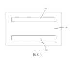
現參照圖1與圖2,圖1提供根據一實施例之沿圖2之線A-A所取得的包括一雙側安裝式封裝結構100的一記憶體模組的截面側視圖圖示。圖2係根據一實施例之雙側安裝式封裝結構100的示意俯視圖圖示。如所繪示,一記憶體模組可包括一電路板200、及安裝在該電路板200上之雙側安裝式封裝結構100。此可使用覆晶接合及焊料凸塊134來達成。1 and FIG. 2, FIG. 1 provides a cross-sectional side view illustration of a memory module including a double-sided mounting
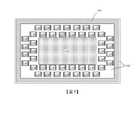
根據實施例之雙側安裝式封裝結構100可包括模組基材102、及安裝在該模組基材102之頂部側103上的第一邏輯晶粒110。雖然繪示的是單個邏輯晶粒110,但可有多個邏輯晶粒110。例如,多個邏輯晶粒110可佔據由在圖2中之第一邏輯晶粒110所繪示之相同周長。一第一複數個記憶體封裝120係安裝在模組基材102之頂部側103上。如圖2所示,第一複數個記憶體封裝120可選地可包括安裝在一或多個邏輯晶粒110之相對側上的第一群組121A及第二群組121B。在模組基材102的底部側105上同樣地安裝一第二複數個記憶體封裝120。該第二複數個記憶體封裝120可安裝在該第一複數個記憶體封裝120正下方,且同樣地可配置在第一群組及第二群組中。The double-sided mounting
所繪示之例示性記憶體封裝120包括複數個記憶體晶粒124,該複數個記憶體晶粒堆疊在基材129上、與銲線126連接、且封裝在模製材料128中。應理解的是,此係一例示性實施方案,且實施例不限於此特定記憶體封裝組態。根據實施例,記憶體封裝120可係包括一或多個DRAM晶粒的DRAM封裝。此外,雙側安裝式封裝結構100可使用各種記憶體技術實施,該等記憶體技術包括LPDDR、LPDDR-x、HBM、HMC等。The illustrated
再次參照圖1,一佈線基材130係安裝至模組基材102之底部側105且在第一邏輯晶粒110(或多個邏輯晶粒110)正下方。該佈線基材130之一底部側133上存在複數個接觸件135。銲料凸塊134可經放置在接觸件135上,用於連接至電路板200。1 again, a
第一佈線係提供通過該佈線基材及該無芯模組基材,以連接在該佈線基材之該底部側上的該複數個接觸件及該第一邏輯晶粒。在一實施例中,通用型輸入/輸出佈線及電源佈線106A延伸通過該佈線基材。此外,通用型輸入/輸出佈線及電源佈線106B延伸通過模組基材102。通用型輸入/輸出佈線及電源佈線106A/B一起將佈線基材130之底部側133上的複數個接觸件135與一或多個邏輯晶粒110連接。The first wiring is provided through the wiring substrate and the coreless module substrate to connect the plurality of contacts and the first logic die on the bottom side of the wiring substrate. In one embodiment, general-purpose input/output wiring and power wiring 106A extend through the wiring substrate. In addition, general-purpose input/output wiring and
第二佈線係設置在該模組基材內,以將第一邏輯晶粒與第一複數個記憶體封裝及第二複數個記憶體封裝兩者連接。在一實施例中,信號佈線104係位於模組基材102內,以將邏輯晶粒110與第一複數個記憶體封裝120及第二複數個記憶體封裝120兩者在模組基材102之相對側上連接。信號佈線104至各記憶體封裝120的長度可例如對應於記憶體通道長度。因此,可藉由將記憶體封裝120安裝在模組基材102的相對側上來減少記憶體通道長度,而非以多個列或較長列將記憶體封裝安裝在一基材之一相同側上。此外,信號佈線104的長度可使用減少的模組基材102之厚度來縮減。在一些實施例中,模組基材102係一無芯模組基材。此可避免形成通過基材核心之通孔的要求。取而代之地,細線圖案化技術可用於模組基材102內的所有佈線。The second wiring is arranged in the module base material to connect the first logic die to both the first plurality of memory packages and the second plurality of memory packages. In one embodiment, the
根據實施例之佈線基材130可比模組基材102更厚。在一些實施例中,佈線基材130可係一層壓佈線基材,且可係一有芯層壓佈線基材。此可允許成本降低,利用較不昂貴的佈線基材130處理,該佈線基材可額外包括比模組基材102更粗的間距及更寬的線寬。此可達成係因為在(多個)邏輯晶粒110與記憶體封裝120之間的信號佈線104係包含在模組基材102中。因此,模組基材102內的信號佈線104之特徵在於比通過佈線基材130之通用型輸入/輸出佈線及電源佈線106A更細的間距及更窄的線寬。一較厚的佈線基材130可額外提供間隙,該間隙用於在電路板200上安裝以及用於放置離散式整合被動裝置(integrated passive device, IPD) 140,諸如電容器陣列,其可提供各種功能,包括電壓調節至邏輯晶粒110之通用型輸入/輸出佈線及電源佈線。一或多個離散式IPD 140可安裝諸如在佈線基材130之底部側133的位置(該底部側橫向相鄰於複數個焊料凸塊134)及模組基材102之底部側105的位置。離散式IPD 140亦可位於佈線基材130內。The
根據實施例之雙側安裝式封裝結構100可包括由於薄模組基材102而用於機械平衡的各種支撐結構。例如,模組基材102可能缺少原本由一厚芯提供的一些機械強度(mechanical robustness)。機械平衡可使用佈線基材130、加強環(stiffener ring) 160、及可選地基材條150之任一者或一組合來達成。在圖1及圖2所繪示之實施例中,一頂部側加強環160經安裝至模組基材102的頂部側103。頂部側加強環160可側向環繞第一複數個記憶體封裝120及(多個)邏輯晶粒110。The double-sided mounting
在圖1所繪示的實施例中,一或多個基材條150經安裝至模組基材102的底部側105。該一或多個基材條150可側向地圍繞第二複數個記憶體封裝120及佈線基材130。在一實施例中,基材條150係由與佈線基材130相同的基材材料所形成,但此並非係必需的。基材條150可選地可在頂部側加強環160正下方。在一實施例中,基材條150可含有額外的電氣佈線(electrical routing)。因此,可使用焊料凸塊132將基材條150以與佈線基材130同樣的方式安裝,可選地位在接觸件155上以用於電氣佈線。銲料凸塊132可係小於焊料凸塊134的微凸塊。In the embodiment shown in FIG. 1, one or more substrate strips 150 are mounted to the
根據實施例之雙側安裝式封裝結構可包括使用焊料凸塊112安裝在模組基材102之頂部側103上的一或多個邏輯晶粒110。如所示,可施加銲料凸塊112至接觸件114。該(等)經安裝之邏輯晶粒110可與一底部填充材料118緊固。如所示,該(等)邏輯晶粒110係與通用型輸入/輸出佈線及電源佈線106B及信號佈線104電連接。第一及第二複數個記憶體封裝120亦可使用焊料凸塊122安裝在模組基材的頂部側及底部側上,且佈線基材可使用焊料凸塊132安裝至模組基材102的底部側105。同樣地,基材條150可使用焊料凸塊132安裝。根據實施例之焊料凸塊112、122、132可全部係微凸塊且具有比焊料凸塊134更小之用於安裝至電路板200的體積/面積。此外,離散式IPD 140亦可使用焊料凸塊142來安裝,焊料凸塊142可係具有比焊料凸塊112、122、132更小之體積/面積的微凸塊。The double-sided mounting type package structure according to the embodiment may include one or more logic dies 110 mounted on the
在諸如繪示在圖2中之一實施例中,一或多個邏輯晶粒110係安裝在封裝100或模組基材102之一中心上。例如,邏輯晶粒110之側向邊緣111可沿著一或多個x軸(由線X-X所繪示)或y軸(由線Y-Y所繪示)而與封裝100之一對應邊緣101等距(該邊緣可對應於模組基材102之一邊緣)。該邏輯晶粒110可另外繞x軸及/或y軸對稱。在另一實施例中,該(等)一或多個邏輯晶粒110未安裝在封裝110或模組基材102之一中心上。In an embodiment such as that shown in FIG. 2, one or more logic dies 110 are mounted on the center of the
現請參照圖3,提供根據一實施例之一佈線基材130內之開口131的示意俯視圖。開口131可完全延伸通過佈線基材130。在此一變化中,第二複數個記憶體封裝120係安裝在模組基材102之底部側105上並在佈線基材130中的該對開口131內,且與佈線基材130側向相鄰。以此方式,佈線基材130可提供額外的機械平衡及對於薄模組基材102的支撐。因此,單一佈線基材130可免除包括額外的基材條150。Referring now to FIG. 3, a schematic top view of an
圖4係又一額外變化。在所提供的特定截面側視圖中,底部側加強環170係安裝至模組基材102之底部側105。該底部側加強環170側向環繞第二複數個記憶體封裝120及佈線基材130。該底部側加強環170可與頂部側加強環160相同。可使用包括黏著劑、焊料等之合適技術附接該頂部側加強環160及該底部側加強環170。Figure 4 is another additional change. In the specific cross-sectional side view provided, the bottom
目前為止已描述各種結構組態,其中可藉由將記憶體封裝120安裝在模組基材102的相對側上來減少記憶體通道長度,而非以多個列或較長列將記憶體封裝安裝在一基材之一相同側上。然而,雙側安裝式MCM封裝結構係額外相容於此組態,特別是用於較大的記憶體縮放。圖5係根據包括多列記憶體封裝之一實施例之一雙側安裝式封裝結構的示意俯視圖圖示。實施例不限於僅包括安裝在一或多個邏輯晶粒110之相對側上的記憶體封裝120之第一群組121A及第二群組121B的組態。如所示,記憶體封裝120可放置於一邏輯晶粒110之多於兩個側上且可圍繞該一或多個邏輯晶粒110。此外,多列記憶體封裝120可圍繞一邏輯晶粒110之一或多個側予以配置,且多列記憶體封裝120可完全地圍繞一邏輯晶粒110予以配置。在所繪示的實施例中,記憶體封裝120之外部列或群組可偏離記憶體封裝120的內部列或群組以允許佈線。類似於圖1及圖3所繪示的實施例,多列記憶體封裝120可安裝至模組基材102之兩側。此外,底部側記憶體封裝可如先前所述地位在記憶體封裝的頂部側正下方。Various structural configurations have been described so far. Among them, the memory channel length can be reduced by mounting the
在使用實施例的各種態樣的過程中,所屬技術領域中具有通常知識者將明白上述實施例的組合或變化對於形成雙側安裝式MCM封裝而言係可行的。雖然已經以結構特徵及/或方法動作之特定語言敘述實施例,應了解附加的申請專利範圍不必受限於所述的特定特徵或行為。替代地,所揭示之特定的特徵或動作應理解為可用於說明之申請專利範圍的實施例。In the process of using the various aspects of the embodiments, those with ordinary knowledge in the art will understand that the combination or changes of the above embodiments are feasible for forming a double-sided mounting type MCM package. Although the embodiments have been described in specific language of structural features and/or method actions, it should be understood that the scope of additional patent applications is not necessarily limited to the specific features or behaviors described. Instead, the specific features or actions disclosed should be understood as embodiments that can be used to illustrate the scope of the patent application.
100:雙側安裝式封裝結構/封裝101:邊緣102:模組基材103:頂部側104:信號佈線105:底部側106A:電源佈線106B:電源佈線110:邏輯晶粒/封裝111:側向邊緣112:焊料凸塊114:接觸件118:底部填充材料120:記憶體封裝121A:第一群組121B:第二群組122:焊料凸塊124:記憶體晶粒126:銲線128:模製材料129:基材130:佈線基材131:開口132:焊料凸塊133:底部側134:銲料凸塊135:接觸件140:離散式整合被動裝置(integrated passive device, IPD)142:焊料凸塊150:基材條155:接觸件160:加強環170:加強環200:電路板A:線X:線Y:線100: Double-side mounting package structure/package101: Edge102: Module base material103: Top side104: signal wiring105: bottom side106A:
[圖1]係根據一實施例之沿圖2之線A-A所取得的包括一雙側安裝式封裝結構的一記憶體模組的截面側視圖圖示。[圖2]係根據一實施例之一雙側安裝式封裝結構的示意俯視圖圖示。[圖3]係根據一實施例之佈線基材內之開口的示意俯視圖圖示。[圖4]係根據一實施例之沿圖2之線A-A所取得的包括一雙側安裝式封裝結構的一記憶體模組的截面側視圖圖示。[圖5]係根據包括多列記憶體封裝之一實施例之一雙側安裝式封裝結構的示意俯視圖圖示。[FIG. 1] is a cross-sectional side view illustration of a memory module including a double-sided mounting type package structure taken along the line A-A of FIG. 2 according to an embodiment.[Fig. 2] is a schematic top view illustration of a double-sided mounting type package structure according to an embodiment.[FIG. 3] is a schematic top view illustration of an opening in a wiring substrate according to an embodiment.[FIG. 4] is a cross-sectional side view illustration of a memory module including a double-sided mounting type package structure taken along the line A-A of FIG. 2 according to an embodiment.[FIG. 5] A schematic top view illustration of a double-side mounting type package structure according to an embodiment of a multi-row memory package.
100:雙側安裝式封裝結構/封裝100: Double-side mounting package structure/package
101:邊緣101: Edge
102:模組基材102: Module base material
103:頂部側103: Top side
104:信號佈線104: signal wiring
105:底部側105: bottom side
106A:電源佈線106A: Power wiring
106B:電源佈線106B: Power wiring
110:邏輯晶粒110: Logic Die
111:側向邊緣111: Lateral edge
112:焊料凸塊112: Solder bump
114:接觸件114: Contact
118:底部填充材料118: Underfill material
120:記憶體封裝120: Memory package
122:焊料凸塊122: Solder bump
124:記憶體晶粒124: memory die
126:銲線126: Welding Wire
128:模製材料128: molding material
129:基材129: Substrate
130:佈線基材130: Wiring substrate
132:焊料凸塊132: Solder bump
133:底部側133: bottom side
134:銲料凸塊134: Solder bump
135:接觸件135: Contact
140:離散式整合被動裝置(integrated passive device,IPD)140: Discrete integrated passive device (IPD)
142:焊料凸塊142: Solder bumps
150:基材條150: substrate strip
155:接觸件155: Contact
160:加強環160: Reinforcement ring
200:電路板200: circuit board
Claims (21)
Translated fromChineseApplications Claiming Priority (2)
| Application Number | Priority Date | Filing Date | Title |
|---|---|---|---|
| US16/204,679US10685948B1 (en) | 2018-11-29 | 2018-11-29 | Double side mounted large MCM package with memory channel length reduction |
| US16/204,679 | 2018-11-29 |
Publications (2)
| Publication Number | Publication Date |
|---|---|
| TW202040787A TW202040787A (en) | 2020-11-01 |
| TWI734271Btrue TWI734271B (en) | 2021-07-21 |
Family
ID=69024592
Family Applications (1)
| Application Number | Title | Priority Date | Filing Date |
|---|---|---|---|
| TW108143068ATWI734271B (en) | 2018-11-29 | 2019-11-27 | Double side mounted large mcm package with memory channel length reduction |
Country Status (4)
| Country | Link |
|---|---|
| US (2) | US10685948B1 (en) |
| CN (1) | CN113169157B (en) |
| TW (1) | TWI734271B (en) |
| WO (1) | WO2020112504A1 (en) |
Families Citing this family (8)
| Publication number | Priority date | Publication date | Assignee | Title |
|---|---|---|---|---|
| US20190157253A1 (en)* | 2019-01-22 | 2019-05-23 | Intel Corporation | Circuit Systems Having Memory Modules With Reverse Orientations |
| KR102764498B1 (en)* | 2019-12-12 | 2025-02-10 | 삼성전자주식회사 | Semiconductor module |
| US11908810B2 (en) | 2020-12-03 | 2024-02-20 | Samsung Electronics Co., Ltd. | Hybrid semiconductor device and electronic device |
| US11728266B2 (en)* | 2020-12-23 | 2023-08-15 | Apple Inc. | Die stitching and harvesting of arrayed structures |
| US20230147273A1 (en)* | 2021-11-05 | 2023-05-11 | Apple Inc. | Warpage Compensation for BGA Package |
| US20230197623A1 (en)* | 2021-12-20 | 2023-06-22 | Advanced Micro Devices, Inc. | Electronic device including an integrated circuit die and a support structure |
| US12278172B2 (en)* | 2022-06-28 | 2025-04-15 | Applied Materials, Inc. | Substrate frame design for three-dimensional stacked electronic assemblies and method for the same |
| US20250112192A1 (en)* | 2023-09-29 | 2025-04-03 | Apple Inc. | 3D System and Wafer Reconstitution with Mid-layer Interposer based on µbump |
Citations (8)
| Publication number | Priority date | Publication date | Assignee | Title |
|---|---|---|---|---|
| TW516209B (en)* | 2000-02-04 | 2003-01-01 | Lucent Technologies Inc | High performance multi-chip IC package |
| US20110140268A1 (en)* | 2009-12-16 | 2011-06-16 | Bok Eng Cheah | High-density inter-package connections for ultra-thin package-on-package structures, and processes of forming same |
| US20120250265A1 (en)* | 2009-12-22 | 2012-10-04 | Murata Manufacturing Co., Ltd. | Circuit module manufacturing method, circuit module, and electronic apparatus including circuit module |
| US9153550B2 (en)* | 2013-11-14 | 2015-10-06 | Taiwan Semiconductor Manufacturing Company, Ltd. | Substrate design with balanced metal and solder resist density |
| US20160372448A1 (en)* | 2015-05-20 | 2016-12-22 | Broadpak Corporation | Semiconductor structure and a method of making thereof |
| WO2017111975A1 (en)* | 2015-12-22 | 2017-06-29 | Intel Corporation | Microelectronic devices with high frequency communication modules having compound semiconductor devices integrated on a package fabric |
| US20170263518A1 (en)* | 2016-03-11 | 2017-09-14 | Taiwan Semiconductor Manufacturing Company, Ltd. | Integrated Fan-Out Package Including Voltage Regulators and Methods Forming Same |
| US9818680B2 (en)* | 2011-07-27 | 2017-11-14 | Broadpak Corporation | Scalable semiconductor interposer integration |
Family Cites Families (6)
| Publication number | Priority date | Publication date | Assignee | Title |
|---|---|---|---|---|
| JP3461172B2 (en)* | 2001-07-05 | 2003-10-27 | 日東電工株式会社 | Method for manufacturing multilayer wiring circuit board |
| KR101274460B1 (en)* | 2011-11-22 | 2013-06-18 | 삼성전기주식회사 | Semiconductor package and manufacturing method threrof |
| JP6200236B2 (en) | 2013-08-09 | 2017-09-20 | ルネサスエレクトロニクス株式会社 | Electronic equipment |
| US9666559B2 (en) | 2014-09-05 | 2017-05-30 | Invensas Corporation | Multichip modules and methods of fabrication |
| CN105518860A (en) | 2014-12-19 | 2016-04-20 | 英特尔Ip公司 | Stack type semiconductor device package with improved interconnection bandwidth |
| US10177161B2 (en) | 2016-12-28 | 2019-01-08 | Intel Corporation | Methods of forming package structures for enhanced memory capacity and structures formed thereby |
- 2018
- 2018-11-29USUS16/204,679patent/US10685948B1/enactiveActive
- 2019
- 2019-11-21WOPCT/US2019/062701patent/WO2020112504A1/ennot_activeCeased
- 2019-11-21CNCN201980079413.4Apatent/CN113169157B/enactiveActive
- 2019-11-27TWTW108143068Apatent/TWI734271B/enactive
- 2020
- 2020-05-21USUS16/880,463patent/US11158621B2/enactiveActive
Patent Citations (8)
| Publication number | Priority date | Publication date | Assignee | Title |
|---|---|---|---|---|
| TW516209B (en)* | 2000-02-04 | 2003-01-01 | Lucent Technologies Inc | High performance multi-chip IC package |
| US20110140268A1 (en)* | 2009-12-16 | 2011-06-16 | Bok Eng Cheah | High-density inter-package connections for ultra-thin package-on-package structures, and processes of forming same |
| US20120250265A1 (en)* | 2009-12-22 | 2012-10-04 | Murata Manufacturing Co., Ltd. | Circuit module manufacturing method, circuit module, and electronic apparatus including circuit module |
| US9818680B2 (en)* | 2011-07-27 | 2017-11-14 | Broadpak Corporation | Scalable semiconductor interposer integration |
| US9153550B2 (en)* | 2013-11-14 | 2015-10-06 | Taiwan Semiconductor Manufacturing Company, Ltd. | Substrate design with balanced metal and solder resist density |
| US20160372448A1 (en)* | 2015-05-20 | 2016-12-22 | Broadpak Corporation | Semiconductor structure and a method of making thereof |
| WO2017111975A1 (en)* | 2015-12-22 | 2017-06-29 | Intel Corporation | Microelectronic devices with high frequency communication modules having compound semiconductor devices integrated on a package fabric |
| US20170263518A1 (en)* | 2016-03-11 | 2017-09-14 | Taiwan Semiconductor Manufacturing Company, Ltd. | Integrated Fan-Out Package Including Voltage Regulators and Methods Forming Same |
Also Published As
| Publication number | Publication date |
|---|---|
| US10685948B1 (en) | 2020-06-16 |
| TW202040787A (en) | 2020-11-01 |
| US20200279842A1 (en) | 2020-09-03 |
| WO2020112504A1 (en) | 2020-06-04 |
| US20200176431A1 (en) | 2020-06-04 |
| CN113169157B (en) | 2023-10-27 |
| US11158621B2 (en) | 2021-10-26 |
| CN113169157A (en) | 2021-07-23 |
Similar Documents
| Publication | Publication Date | Title |
|---|---|---|
| TWI734271B (en) | Double side mounted large mcm package with memory channel length reduction | |
| TWI733542B (en) | Package structure and manufacturing method thereof | |
| US8502370B2 (en) | Stack package structure and fabrication method thereof | |
| US9406618B2 (en) | Die-stacking using through-silicon vias on bumpless build-up layer substrates including embedded-dice, and processes of forming same | |
| US8664780B2 (en) | Semiconductor package having plural semiconductor chips and method of forming the same | |
| US7598617B2 (en) | Stack package utilizing through vias and re-distribution lines | |
| US20150201497A1 (en) | High-density inter-package connections for ultra-thin package-on-package structures, and processes of forming same | |
| TW201826461A (en) | Stacked type chip package structure | |
| US8674516B2 (en) | Integrated circuit packaging system with vertical interconnects and method of manufacture thereof | |
| US12136590B2 (en) | Semiconductor package and method of manufacturing the same | |
| KR101096455B1 (en) | Heat dissipation unit, its manufacturing method and stack package using same | |
| US8736076B2 (en) | Multi-chip stacking of integrated circuit devices using partial device overlap | |
| US9318470B2 (en) | Semiconductor device | |
| US20160079210A1 (en) | Semiconductor packages including through electrodes and methods of manufacturing the same | |
| CN101465341A (en) | Stacked chip packaging structure | |
| TWI605555B (en) | Package structure and the manufacture thereof | |
| KR20060074091A (en) | Chip stack package | |
| US20240055333A1 (en) | Semiconductor structure and method for manufacturing same | |
| KR100851108B1 (en) | Wafer level system in package and fabrication method thereof | |
| TWI227552B (en) | Stacked chip package structure | |
| CN112908868A (en) | Three-dimensional packaging method and structure of memory | |
| TW202406064A (en) | Package structure and manufacturing method thereof | |
| CN117650132A (en) | Semiconductor structure and method for manufacturing semiconductor structure |