TWI734185B - Plasma processing apparatus - Google Patents
Plasma processing apparatusDownload PDFInfo
- Publication number
- TWI734185B TWI734185BTW108131630ATW108131630ATWI734185BTW I734185 BTWI734185 BTW I734185BTW 108131630 ATW108131630 ATW 108131630ATW 108131630 ATW108131630 ATW 108131630ATW I734185 BTWI734185 BTW I734185B
- Authority
- TW
- Taiwan
- Prior art keywords
- electrode
- frequency power
- ring
- plasma
- plasma processing
- Prior art date
Links
- 239000000758substrateSubstances0.000claimsabstractdescription73
- 239000010409thin filmSubstances0.000claimsabstractdescription43
- 239000000463materialSubstances0.000claimsabstractdescription14
- 239000010408filmSubstances0.000claimsdescription34
- 230000002093peripheral effectEffects0.000claimsdescription26
- WFKWXMTUELFFGS-UHFFFAOYSA-NtungstenChemical compound[W]WFKWXMTUELFFGS-UHFFFAOYSA-N0.000claimsdescription9
- 229910052721tungstenInorganic materials0.000claimsdescription9
- 239000010937tungstenSubstances0.000claimsdescription9
- 238000005507sprayingMethods0.000claimsdescription7
- 239000003989dielectric materialSubstances0.000claimsdescription5
- TWNQGVIAIRXVLR-UHFFFAOYSA-Noxo(oxoalumanyloxy)alumaneChemical compoundO=[Al]O[Al]=OTWNQGVIAIRXVLR-UHFFFAOYSA-N0.000claimsdescription5
- 239000011810insulating materialSubstances0.000claimsdescription4
- 238000009832plasma treatmentMethods0.000claims1
- 235000012431wafersNutrition0.000description81
- 239000004020conductorSubstances0.000description29
- 238000005530etchingMethods0.000description29
- 239000007789gasSubstances0.000description28
- 230000005684electric fieldEffects0.000description25
- 239000004065semiconductorSubstances0.000description20
- 230000008878couplingEffects0.000description17
- 238000010168coupling processMethods0.000description17
- 238000005859coupling reactionMethods0.000description17
- 238000000034methodMethods0.000description17
- 230000008569processEffects0.000description16
- 239000003507refrigerantSubstances0.000description10
- 239000002245particleSubstances0.000description7
- 238000001179sorption measurementMethods0.000description7
- 239000002826coolantSubstances0.000description5
- 239000012212insulatorSubstances0.000description5
- 238000001020plasma etchingMethods0.000description5
- 239000007921spraySubstances0.000description5
- 238000009413insulationMethods0.000description4
- 230000000694effectsEffects0.000description3
- 238000002347injectionMethods0.000description3
- 239000007924injectionSubstances0.000description3
- 239000010453quartzSubstances0.000description3
- VYPSYNLAJGMNEJ-UHFFFAOYSA-Nsilicon dioxideInorganic materialsO=[Si]=OVYPSYNLAJGMNEJ-UHFFFAOYSA-N0.000description3
- 230000002159abnormal effectEffects0.000description2
- 238000005513bias potentialMethods0.000description2
- 238000005516engineering processMethods0.000description2
- 150000002500ionsChemical class0.000description2
- 229910052751metalInorganic materials0.000description2
- 239000002184metalSubstances0.000description2
- 230000002035prolonged effectEffects0.000description2
- PNEYBMLMFCGWSK-UHFFFAOYSA-Naluminium oxideInorganic materials[O-2].[O-2].[O-2].[Al+3].[Al+3]PNEYBMLMFCGWSK-UHFFFAOYSA-N0.000description1
- 239000000919ceramicSubstances0.000description1
- 230000008859changeEffects0.000description1
- 238000010586diagramMethods0.000description1
- 230000005611electricityEffects0.000description1
- 239000001307heliumSubstances0.000description1
- 229910052734heliumInorganic materials0.000description1
- SWQJXJOGLNCZEY-UHFFFAOYSA-Nhelium atomChemical compound[He]SWQJXJOGLNCZEY-UHFFFAOYSA-N0.000description1
- 230000010354integrationEffects0.000description1
- 238000004519manufacturing processMethods0.000description1
- 239000012528membraneSubstances0.000description1
- 238000011084recoveryMethods0.000description1
- 230000009467reductionEffects0.000description1
- 230000003252repetitive effectEffects0.000description1
- 230000004044responseEffects0.000description1
- 230000003068static effectEffects0.000description1
- 239000000725suspensionSubstances0.000description1
- 230000003685thermal hair damageEffects0.000description1
- 238000007751thermal sprayingMethods0.000description1
Images


Classifications
- H—ELECTRICITY
- H01—ELECTRIC ELEMENTS
- H01J—ELECTRIC DISCHARGE TUBES OR DISCHARGE LAMPS
- H01J37/00—Discharge tubes with provision for introducing objects or material to be exposed to the discharge, e.g. for the purpose of examination or processing thereof
- H01J37/32—Gas-filled discharge tubes
- H01J37/32431—Constructional details of the reactor
- H01J37/32532—Electrodes
- C—CHEMISTRY; METALLURGY
- C23—COATING METALLIC MATERIAL; COATING MATERIAL WITH METALLIC MATERIAL; CHEMICAL SURFACE TREATMENT; DIFFUSION TREATMENT OF METALLIC MATERIAL; COATING BY VACUUM EVAPORATION, BY SPUTTERING, BY ION IMPLANTATION OR BY CHEMICAL VAPOUR DEPOSITION, IN GENERAL; INHIBITING CORROSION OF METALLIC MATERIAL OR INCRUSTATION IN GENERAL
- C23C—COATING METALLIC MATERIAL; COATING MATERIAL WITH METALLIC MATERIAL; SURFACE TREATMENT OF METALLIC MATERIAL BY DIFFUSION INTO THE SURFACE, BY CHEMICAL CONVERSION OR SUBSTITUTION; COATING BY VACUUM EVAPORATION, BY SPUTTERING, BY ION IMPLANTATION OR BY CHEMICAL VAPOUR DEPOSITION, IN GENERAL
- C23C14/00—Coating by vacuum evaporation, by sputtering or by ion implantation of the coating forming material
- C23C14/22—Coating by vacuum evaporation, by sputtering or by ion implantation of the coating forming material characterised by the process of coating
- C23C14/50—Substrate holders
- C—CHEMISTRY; METALLURGY
- C23—COATING METALLIC MATERIAL; COATING MATERIAL WITH METALLIC MATERIAL; CHEMICAL SURFACE TREATMENT; DIFFUSION TREATMENT OF METALLIC MATERIAL; COATING BY VACUUM EVAPORATION, BY SPUTTERING, BY ION IMPLANTATION OR BY CHEMICAL VAPOUR DEPOSITION, IN GENERAL; INHIBITING CORROSION OF METALLIC MATERIAL OR INCRUSTATION IN GENERAL
- C23C—COATING METALLIC MATERIAL; COATING MATERIAL WITH METALLIC MATERIAL; SURFACE TREATMENT OF METALLIC MATERIAL BY DIFFUSION INTO THE SURFACE, BY CHEMICAL CONVERSION OR SUBSTITUTION; COATING BY VACUUM EVAPORATION, BY SPUTTERING, BY ION IMPLANTATION OR BY CHEMICAL VAPOUR DEPOSITION, IN GENERAL
- C23C16/00—Chemical coating by decomposition of gaseous compounds, without leaving reaction products of surface material in the coating, i.e. chemical vapour deposition [CVD] processes
- C23C16/44—Chemical coating by decomposition of gaseous compounds, without leaving reaction products of surface material in the coating, i.e. chemical vapour deposition [CVD] processes characterised by the method of coating
- C23C16/458—Chemical coating by decomposition of gaseous compounds, without leaving reaction products of surface material in the coating, i.e. chemical vapour deposition [CVD] processes characterised by the method of coating characterised by the method used for supporting substrates in the reaction chamber
- C23C16/4582—Rigid and flat substrates, e.g. plates or discs
- C23C16/4583—Rigid and flat substrates, e.g. plates or discs the substrate being supported substantially horizontally
- H—ELECTRICITY
- H01—ELECTRIC ELEMENTS
- H01J—ELECTRIC DISCHARGE TUBES OR DISCHARGE LAMPS
- H01J37/00—Discharge tubes with provision for introducing objects or material to be exposed to the discharge, e.g. for the purpose of examination or processing thereof
- H01J37/32—Gas-filled discharge tubes
- H01J37/32009—Arrangements for generation of plasma specially adapted for examination or treatment of objects, e.g. plasma sources
- H01J37/32082—Radio frequency generated discharge
- H01J37/321—Radio frequency generated discharge the radio frequency energy being inductively coupled to the plasma
- H01J37/32119—Windows
- H—ELECTRICITY
- H01—ELECTRIC ELEMENTS
- H01J—ELECTRIC DISCHARGE TUBES OR DISCHARGE LAMPS
- H01J37/00—Discharge tubes with provision for introducing objects or material to be exposed to the discharge, e.g. for the purpose of examination or processing thereof
- H01J37/32—Gas-filled discharge tubes
- H01J37/32009—Arrangements for generation of plasma specially adapted for examination or treatment of objects, e.g. plasma sources
- H01J37/32082—Radio frequency generated discharge
- H01J37/32174—Circuits specially adapted for controlling the RF discharge
- H—ELECTRICITY
- H01—ELECTRIC ELEMENTS
- H01J—ELECTRIC DISCHARGE TUBES OR DISCHARGE LAMPS
- H01J37/00—Discharge tubes with provision for introducing objects or material to be exposed to the discharge, e.g. for the purpose of examination or processing thereof
- H01J37/32—Gas-filled discharge tubes
- H01J37/32009—Arrangements for generation of plasma specially adapted for examination or treatment of objects, e.g. plasma sources
- H01J37/32192—Microwave generated discharge
- H01J37/32201—Generating means
- H—ELECTRICITY
- H01—ELECTRIC ELEMENTS
- H01J—ELECTRIC DISCHARGE TUBES OR DISCHARGE LAMPS
- H01J37/00—Discharge tubes with provision for introducing objects or material to be exposed to the discharge, e.g. for the purpose of examination or processing thereof
- H01J37/32—Gas-filled discharge tubes
- H01J37/32009—Arrangements for generation of plasma specially adapted for examination or treatment of objects, e.g. plasma sources
- H01J37/32192—Microwave generated discharge
- H01J37/32302—Plural frequencies
- H—ELECTRICITY
- H01—ELECTRIC ELEMENTS
- H01J—ELECTRIC DISCHARGE TUBES OR DISCHARGE LAMPS
- H01J37/00—Discharge tubes with provision for introducing objects or material to be exposed to the discharge, e.g. for the purpose of examination or processing thereof
- H01J37/32—Gas-filled discharge tubes
- H01J37/32009—Arrangements for generation of plasma specially adapted for examination or treatment of objects, e.g. plasma sources
- H01J37/32192—Microwave generated discharge
- H01J37/32311—Circuits specially adapted for controlling the microwave discharge
- H—ELECTRICITY
- H01—ELECTRIC ELEMENTS
- H01J—ELECTRIC DISCHARGE TUBES OR DISCHARGE LAMPS
- H01J37/00—Discharge tubes with provision for introducing objects or material to be exposed to the discharge, e.g. for the purpose of examination or processing thereof
- H01J37/32—Gas-filled discharge tubes
- H01J37/32431—Constructional details of the reactor
- H01J37/32458—Vessel
- H01J37/32513—Sealing means, e.g. sealing between different parts of the vessel
- H—ELECTRICITY
- H01—ELECTRIC ELEMENTS
- H01J—ELECTRIC DISCHARGE TUBES OR DISCHARGE LAMPS
- H01J37/00—Discharge tubes with provision for introducing objects or material to be exposed to the discharge, e.g. for the purpose of examination or processing thereof
- H01J37/32—Gas-filled discharge tubes
- H01J37/32431—Constructional details of the reactor
- H01J37/32532—Electrodes
- H01J37/3255—Material
- H—ELECTRICITY
- H01—ELECTRIC ELEMENTS
- H01J—ELECTRIC DISCHARGE TUBES OR DISCHARGE LAMPS
- H01J37/00—Discharge tubes with provision for introducing objects or material to be exposed to the discharge, e.g. for the purpose of examination or processing thereof
- H01J37/32—Gas-filled discharge tubes
- H01J37/32431—Constructional details of the reactor
- H01J37/32532—Electrodes
- H01J37/32568—Relative arrangement or disposition of electrodes; moving means
- H—ELECTRICITY
- H01—ELECTRIC ELEMENTS
- H01J—ELECTRIC DISCHARGE TUBES OR DISCHARGE LAMPS
- H01J37/00—Discharge tubes with provision for introducing objects or material to be exposed to the discharge, e.g. for the purpose of examination or processing thereof
- H01J37/32—Gas-filled discharge tubes
- H01J37/32431—Constructional details of the reactor
- H01J37/32623—Mechanical discharge control means
- H01J37/32642—Focus rings
- H—ELECTRICITY
- H01—ELECTRIC ELEMENTS
- H01J—ELECTRIC DISCHARGE TUBES OR DISCHARGE LAMPS
- H01J37/00—Discharge tubes with provision for introducing objects or material to be exposed to the discharge, e.g. for the purpose of examination or processing thereof
- H01J37/32—Gas-filled discharge tubes
- H01J37/32431—Constructional details of the reactor
- H01J37/3266—Magnetic control means
- H—ELECTRICITY
- H01—ELECTRIC ELEMENTS
- H01J—ELECTRIC DISCHARGE TUBES OR DISCHARGE LAMPS
- H01J37/00—Discharge tubes with provision for introducing objects or material to be exposed to the discharge, e.g. for the purpose of examination or processing thereof
- H01J37/32—Gas-filled discharge tubes
- H01J37/32431—Constructional details of the reactor
- H01J37/32715—Workpiece holder
- H—ELECTRICITY
- H01—ELECTRIC ELEMENTS
- H01J—ELECTRIC DISCHARGE TUBES OR DISCHARGE LAMPS
- H01J37/00—Discharge tubes with provision for introducing objects or material to be exposed to the discharge, e.g. for the purpose of examination or processing thereof
- H01J37/32—Gas-filled discharge tubes
- H01J37/32431—Constructional details of the reactor
- H01J37/32798—Further details of plasma apparatus not provided for in groups H01J37/3244 - H01J37/32788; special provisions for cleaning or maintenance of the apparatus
- H01J37/32807—Construction (includes replacing parts of the apparatus)
- H—ELECTRICITY
- H01—ELECTRIC ELEMENTS
- H01L—SEMICONDUCTOR DEVICES NOT COVERED BY CLASS H10
- H01L21/00—Processes or apparatus adapted for the manufacture or treatment of semiconductor or solid state devices or of parts thereof
- H01L21/67—Apparatus specially adapted for handling semiconductor or electric solid state devices during manufacture or treatment thereof; Apparatus specially adapted for handling wafers during manufacture or treatment of semiconductor or electric solid state devices or components ; Apparatus not specifically provided for elsewhere
- H01L21/67005—Apparatus not specifically provided for elsewhere
- H01L21/67011—Apparatus for manufacture or treatment
- H01L21/67017—Apparatus for fluid treatment
- H01L21/67063—Apparatus for fluid treatment for etching
- H01L21/67069—Apparatus for fluid treatment for etching for drying etching
- H—ELECTRICITY
- H01—ELECTRIC ELEMENTS
- H01L—SEMICONDUCTOR DEVICES NOT COVERED BY CLASS H10
- H01L21/00—Processes or apparatus adapted for the manufacture or treatment of semiconductor or solid state devices or of parts thereof
- H01L21/67—Apparatus specially adapted for handling semiconductor or electric solid state devices during manufacture or treatment thereof; Apparatus specially adapted for handling wafers during manufacture or treatment of semiconductor or electric solid state devices or components ; Apparatus not specifically provided for elsewhere
- H01L21/67005—Apparatus not specifically provided for elsewhere
- H01L21/67011—Apparatus for manufacture or treatment
- H01L21/67098—Apparatus for thermal treatment
- H01L21/67109—Apparatus for thermal treatment mainly by convection
- H—ELECTRICITY
- H01—ELECTRIC ELEMENTS
- H01L—SEMICONDUCTOR DEVICES NOT COVERED BY CLASS H10
- H01L21/00—Processes or apparatus adapted for the manufacture or treatment of semiconductor or solid state devices or of parts thereof
- H01L21/67—Apparatus specially adapted for handling semiconductor or electric solid state devices during manufacture or treatment thereof; Apparatus specially adapted for handling wafers during manufacture or treatment of semiconductor or electric solid state devices or components ; Apparatus not specifically provided for elsewhere
- H01L21/683—Apparatus specially adapted for handling semiconductor or electric solid state devices during manufacture or treatment thereof; Apparatus specially adapted for handling wafers during manufacture or treatment of semiconductor or electric solid state devices or components ; Apparatus not specifically provided for elsewhere for supporting or gripping
- H01L21/6831—Apparatus specially adapted for handling semiconductor or electric solid state devices during manufacture or treatment thereof; Apparatus specially adapted for handling wafers during manufacture or treatment of semiconductor or electric solid state devices or components ; Apparatus not specifically provided for elsewhere for supporting or gripping using electrostatic chucks
- H01L21/6833—Details of electrostatic chucks
- H—ELECTRICITY
- H01—ELECTRIC ELEMENTS
- H01L—SEMICONDUCTOR DEVICES NOT COVERED BY CLASS H10
- H01L21/00—Processes or apparatus adapted for the manufacture or treatment of semiconductor or solid state devices or of parts thereof
- H01L21/67—Apparatus specially adapted for handling semiconductor or electric solid state devices during manufacture or treatment thereof; Apparatus specially adapted for handling wafers during manufacture or treatment of semiconductor or electric solid state devices or components ; Apparatus not specifically provided for elsewhere
- H01L21/683—Apparatus specially adapted for handling semiconductor or electric solid state devices during manufacture or treatment thereof; Apparatus specially adapted for handling wafers during manufacture or treatment of semiconductor or electric solid state devices or components ; Apparatus not specifically provided for elsewhere for supporting or gripping
- H01L21/687—Apparatus specially adapted for handling semiconductor or electric solid state devices during manufacture or treatment thereof; Apparatus specially adapted for handling wafers during manufacture or treatment of semiconductor or electric solid state devices or components ; Apparatus not specifically provided for elsewhere for supporting or gripping using mechanical means, e.g. chucks, clamps or pinches
- H01L21/68714—Apparatus specially adapted for handling semiconductor or electric solid state devices during manufacture or treatment thereof; Apparatus specially adapted for handling wafers during manufacture or treatment of semiconductor or electric solid state devices or components ; Apparatus not specifically provided for elsewhere for supporting or gripping using mechanical means, e.g. chucks, clamps or pinches the wafers being placed on a susceptor, stage or support
- H01L21/68735—Apparatus specially adapted for handling semiconductor or electric solid state devices during manufacture or treatment thereof; Apparatus specially adapted for handling wafers during manufacture or treatment of semiconductor or electric solid state devices or components ; Apparatus not specifically provided for elsewhere for supporting or gripping using mechanical means, e.g. chucks, clamps or pinches the wafers being placed on a susceptor, stage or support characterised by edge profile or support profile
- H—ELECTRICITY
- H01—ELECTRIC ELEMENTS
- H01J—ELECTRIC DISCHARGE TUBES OR DISCHARGE LAMPS
- H01J2237/00—Discharge tubes exposing object to beam, e.g. for analysis treatment, etching, imaging
- H01J2237/32—Processing objects by plasma generation
- H01J2237/33—Processing objects by plasma generation characterised by the type of processing
- H01J2237/334—Etching
- H01J2237/3343—Problems associated with etching
Landscapes
- Engineering & Computer Science (AREA)
- Chemical & Material Sciences (AREA)
- Physics & Mathematics (AREA)
- Plasma & Fusion (AREA)
- Analytical Chemistry (AREA)
- Power Engineering (AREA)
- General Physics & Mathematics (AREA)
- Manufacturing & Machinery (AREA)
- Computer Hardware Design (AREA)
- Microelectronics & Electronic Packaging (AREA)
- Condensed Matter Physics & Semiconductors (AREA)
- Chemical Kinetics & Catalysis (AREA)
- Materials Engineering (AREA)
- Mechanical Engineering (AREA)
- Metallurgy (AREA)
- Organic Chemistry (AREA)
- General Chemical & Material Sciences (AREA)
- Drying Of Semiconductors (AREA)
- Plasma Technology (AREA)
- Coating By Spraying Or Casting (AREA)
Abstract
Translated fromChineseDescription
Translated fromChinese本發明關於電漿處理裝置,特別是關於產生電漿對半導體基板等進行蝕刻處理的電漿處理裝置。The present invention relates to a plasma processing device, and more particularly to a plasma processing device that generates plasma to perform etching processing on semiconductor substrates and the like.
伴隨著半導體元件之集積度之提升,電路構造變微細化,製程複雜化。在這樣的狀況下,為了抑制半導體元件之單價之上升,要求提高從1片晶圓能夠獲取的半導體元件之產量,要求直至被處理晶圓之外周緣能夠以高良品率製造性能良好的半導體元件。With the increase in the integration of semiconductor components, the circuit structure has become finer and the manufacturing process has become more complicated. Under such circumstances, in order to suppress the increase in the unit price of semiconductor components, it is required to increase the output of semiconductor components that can be obtained from one wafer, and it is required to produce semiconductor components with high yield and good performance up to the outer periphery of the processed wafer. .
應對這樣的要求,在電漿處理裝置中,要求藉由電漿處理裝置進行處理而在被處理晶圓上形成的半導體元件之性能,在被處理晶圓之面內從中心至周邊部成為均勻。In response to such demands, in plasma processing equipment, the performance of semiconductor elements formed on the processed wafer by the plasma processing equipment is required to be uniform from the center to the periphery of the processed wafer. .
電漿處理裝置亦即蝕刻裝置中,伴隨著電路圖案之微細化,要求奈米、次奈米等級之加工均勻性之精度。為了在遍及被處理晶圓之全面能夠確保這樣的奈米、次奈米等級之加工均勻性之精度,將加工精度容易降低的被處理晶圓之外周部附近中的電漿處理之精度進行提升成為重要。In plasma processing equipment, that is, etching equipment, with the miniaturization of circuit patterns, the precision of processing uniformity at the nanometer and sub-nanometer level is required. In order to ensure the accuracy of such nano- and sub-nano-level processing uniformity throughout the processed wafer, the accuracy of plasma processing in the vicinity of the outer periphery of the processed wafer, which is likely to be reduced, is improved Become important.
蝕刻處理裝置中,在被處理晶圓之外周部附近,基於電磁學、熱力學的因素,相對於被處理晶圓之中央部分,在外周部附近之部分,其之被處理的圖案之加工形狀精度等之蝕刻處理之特性之偏差容易變大。此一現象隨著被處理晶圓之尺寸(外徑)變大而越發顯著。其結果,基於電漿蝕刻處理的被處理晶圓之外周部附近之加工形狀相對於中央部附近之加工精度超出偏差之容許範圍,而發生形成於被處理晶圓之外周部附近的半導體元件無法作為製品出廠之情況。In the etching processing device, the processing shape accuracy of the processed pattern near the outer periphery of the processed wafer based on electromagnetic and thermodynamic factors relative to the central portion of the processed wafer and the portion near the outer periphery of the processed wafer The deviation of the characteristics of the etching process is likely to become large. This phenomenon becomes more pronounced as the size (outer diameter) of the processed wafer becomes larger. As a result, the processed shape near the outer periphery of the processed wafer by plasma etching process exceeds the tolerance of the processing accuracy near the center, and semiconductor elements formed near the outer periphery of the processed wafer cannot As the product leaving the factory.
作為防止這樣的被處理晶圓之外周部附近之加工形狀相對於中央部附近之加工精度超出偏差之容許範圍之手段,於專利文獻1記載有,在載置被處理晶圓的基板電極之周圍,設置與基板電極為同一電位之高頻環,減低高頻偏壓電力之變更之影響,改善被處理晶圓之外周部附近之加工特性而可以提升處理之均勻性的電漿處理裝置。As a means to prevent the processed shape near the outer periphery of the wafer to be processed from exceeding the tolerance of the processing accuracy near the center portion, it is described in Patent Document 1 that around the substrate electrode on which the processed wafer is placed , Plasma processing equipment that is equipped with a high-frequency ring with the same potential as the substrate electrode to reduce the effect of changes in high-frequency bias power, improve the processing characteristics near the outer periphery of the processed wafer, and improve the uniformity of processing.
又,專利文獻2記載有,在載置被處理晶圓的試料台之基材之周圍,在與試料台之基材電氣絕緣之狀態下設置導體環,從與對試料台之基材施加的高頻電力不同的電源對導體環供給高頻電力的構成。[先前技術文獻][專利文獻]In addition, Patent Document 2 describes that a conductor ring is provided around the substrate of the sample table on which the wafer to be processed is placed, and is electrically insulated from the substrate of the sample table. A power supply with different high-frequency power supplies high-frequency power to the conductor loop.[Prior Technical Literature][Patent Literature]
[專利文獻1]特開2014-17292號公報[專利文獻2]特開2016-225376號公報[Patent Document 1] JP 2014-17292 A[Patent Document 2] JP 2016-225376 A
[發明所欲解決之課題][The problem to be solved by the invention]
於蝕刻處理裝置中,藉由電漿處理被處理晶圓時,在載置被處理晶圓的基板電極之外周部附近所形成的電場之形狀影響到電漿處理之均勻性。專利文獻1記載的方法中,基板電極與高頻環為同一電位,因此施加於基板電極的高頻電力在某一條件之情況下即使將基板電極之外周部附近所形成的電場調整為理想狀態時,變化施加於基板電極的高頻電力之條件之情況下,藉由高頻環來調整基板電極之外周部附近所形成的電場是困難的,對被處理晶圓直至外周部附近實施均勻的處理是困難的。In the etching processing apparatus, when the processed wafer is processed by plasma, the shape of the electric field formed near the outer periphery of the substrate electrode on which the processed wafer is placed affects the uniformity of the plasma processing. In the method described in Patent Document 1, the substrate electrode and the high-frequency ring are at the same potential. Therefore, the high-frequency power applied to the substrate electrode is adjusted to an ideal state even if the electric field formed near the outer periphery of the substrate electrode is adjusted to an ideal state under certain conditions. When the conditions of the high-frequency power applied to the substrate electrode are changed, it is difficult to adjust the electric field formed near the outer periphery of the substrate electrode by the high-frequency ring, and it is difficult to uniformly process the wafer to be processed up to the periphery of the outer periphery. .
另一方面,晶圓外周部之電場失真時,晶圓之表面與其上之電漿區域之境界的鞘區域中形成的電場之等電位面會發生不均勻或形狀之傾斜。鞘區域中,離子在相對於等電位面為直角的方向受力,因此若等電位面相對於晶圓之面傾斜,則射入晶圓的離子在接受到與等電位面之傾斜對應的傾斜方向之力的狀態下射入晶圓。其結果存在有如在晶圓上所形成的圖案之形狀產生分布,或晶圓外周部之由絕緣體形成的環之消耗被加速等之問題。On the other hand, when the electric field at the outer periphery of the wafer is distorted, the equipotential surface of the electric field formed in the sheath area between the surface of the wafer and the plasma area on it will be uneven or inclined in shape. In the sheath area, the ions receive force at a right angle to the equipotential surface. Therefore, if the equipotential surface is inclined with respect to the surface of the wafer, the ions injected into the wafer receive the inclination direction corresponding to the inclination of the equipotential surface. Inject into the wafer under the power of the force. As a result, there are problems such as the distribution of the shape of the pattern formed on the wafer, or the accelerated consumption of the ring formed by the insulator on the outer periphery of the wafer.
相對於此,專利文獻2記載的構成中,為了對試料台之基材(基板電極)之外周部所產生的鞘區域中的電場之傾斜進行補正,在試料台之基材之外周部所配置的絕緣體之環之上配置導體環(高頻環電極),對該導體環施加和施加於試料台之基材的高頻電力為不同控制的高頻電力之構成。In contrast to this, in the structure described in Patent Document 2, in order to correct the inclination of the electric field in the sheath region generated on the outer periphery of the base material (substrate electrode) of the sample stage, it is arranged on the outer periphery of the base material of the sample stage. A conductor ring (high-frequency ring electrode) is arranged on the ring of the insulator, and the high-frequency power applied to the conductor ring and the base material of the sample table is a structure of differently controlled high-frequency power.
但是,夾持著介質而對試料台之基材與導體環分別從不同的電源施加高頻電力之情況下,基於試料台之基材與導體環之間產生的容量耦合,施加於試料台之基材的高頻電力與施加於導體環的高頻電力之間會產生干擾,電力比較小的施加於導體環的高頻電力變為無法控制,試料台之基材所載置的晶圓外周部之電場有可能失真。However, when high-frequency power is applied from different power sources to the substrate and the conductor ring of the sample table while holding the medium, the capacitance coupling between the substrate and the conductor ring of the sample table is applied to the sample table. Interference occurs between the high-frequency power of the substrate and the high-frequency power applied to the conductor ring. The high-frequency power applied to the conductor ring becomes uncontrollable. The outer periphery of the wafer placed on the substrate of the sample table is uncontrollable. The electric field may be distorted.
本發明為了解決上述習知技術之課題,目的在於提供即使變化施加於基板電極的高頻電力之情況下,亦能夠穩定地控制施加於高頻環電極的高頻電力,減少基板電極之外周部附近之鞘區域所形成的電場之形狀對電漿處理之均勻性帶來的影響,直至被處理晶圓之外周部附近之範圍提升電漿處理之均勻性,使從1片晶圓能夠製造的良品元件之數量更多的技術。[解決課題之手段]In order to solve the above-mentioned problems of the conventional technology, the present invention aims to provide a stable control of the high-frequency power applied to the high-frequency ring electrode even when the high-frequency power applied to the substrate electrode is changed, so as to reduce the amount of energy in the vicinity of the outer periphery of the substrate electrode. The shape of the electric field formed in the sheath area affects the uniformity of plasma processing until the area near the outer periphery of the processed wafer. The uniformity of plasma processing is improved, so that good-quality components can be manufactured from one wafer. The number of technologies is greater.[Means to solve the problem]
為了解決上述課題,本發明中,電漿處理裝置構成為具備:真空容器;載置台,其具備在該真空容器之內部用於載置被處理試料的電極基材,及覆蓋該電極基材之外周部分的由絕緣性之材料形成的承受器環,及被該承受器環覆蓋且以圍繞電極基材之外周的方式被配置,在上面和與電極基材之外周對置之面之一部分形成有薄膜電極的絕緣環;第1高頻電力施加部,對該載置台之電極基材施加第1高頻電力;第2高頻電力施加部,對形成於絕緣環的薄膜電極施加第2高頻電力;電漿產生手段,於真空容器之內部在載置台之上部產生電漿;及控制部,對第1高頻電力施加部與第2高頻電力施加部與電漿產生手段進行控制。[發明效果]In order to solve the above-mentioned problems, in the present invention, the plasma processing apparatus is configured to include: a vacuum container; A susceptor ring formed of an insulating material in the outer peripheral part, and the susceptor ring is covered by the susceptor ring and arranged to surround the outer circumference of the electrode base material, and is formed on the upper surface and a part of the surface facing the outer circumference of the electrode base material Insulating ring with thin-film electrodes; the first high-frequency power application section applies the first high-frequency power to the electrode substrate of the mounting table; the second high-frequency power application section applies the second high-frequency power to the thin-film electrode formed on the insulating ring High-frequency power; Plasma generating means, which generates plasma on the upper part of the mounting table inside the vacuum container; and a control section, which controls the first high-frequency power applying section and the second high-frequency power applying section and the plasma generating means.[Effects of the invention]
依據本發明,可以從被處理晶圓之中心部分至外周部附近為止提升電漿處理之均勻性,從1片晶圓可以取得的良品元件之數(良品之良品率)可以更多。According to the present invention, the uniformity of plasma processing can be improved from the center portion of the processed wafer to the vicinity of the outer periphery, and the number of good components (yield rate of good products) that can be obtained from one wafer can be increased.
又,依據本發明,可以延長配置於晶圓外周部的環狀構件之壽命,減少部品交換之頻度提升電漿處理裝置之裝置運轉率。In addition, according to the present invention, the life of the ring-shaped member disposed on the outer periphery of the wafer can be prolonged, the frequency of parts exchange can be reduced, and the operation rate of the plasma processing device can be improved.
本發明中,為了提升以圍繞基板電極之周圍的方式設置的環電極之控制性,因此使環電極,在介質之表面藉由薄膜形成且將其與基板電極之距離盡可能設為較大,而可以縮小基板電極與環電極之間產生的容量耦合。其結果,對基板電極與環電極從不同之電源分別施加高頻電力時,可以縮小距離比較近的基板電極與環電極之間產生的容量耦合造成的高頻電力之干擾之程度,可以提升基於環電極的表面電位之控制性。In the present invention, in order to improve the controllability of the ring electrode arranged around the substrate electrode, the ring electrode is formed by a thin film on the surface of the medium and the distance between the ring electrode and the substrate electrode is set as large as possible. The capacitance coupling between the substrate electrode and the ring electrode can be reduced. As a result, when high-frequency power is applied to the substrate electrode and the ring electrode from different power sources, it is possible to reduce the interference of the high-frequency power caused by the capacitive coupling between the substrate electrode and the ring electrode that are relatively close, and to improve the Controllability of the surface potential of the ring electrode.
據此,可以縮小基板電極之外周部附近所形成的鞘區域對電漿處理之均勻性帶來的影響,直至被處理晶圓之外周部附近可以均勻地進行電漿處理,從1片晶圓可以取得的良品元件之數量可以更多。According to this, the influence of the sheath area formed near the outer periphery of the substrate electrode on the uniformity of plasma processing can be reduced, and the plasma processing can be uniformly performed near the outer periphery of the processed wafer. The number of good components that can be obtained can be more.
又,本發明中,為了盡可能增大基板電極與環電極之間之距離,減少2個電極之間之容量耦合,因此將環電極,在卷繞基板電極之由絕緣性之材料形成的環狀構件之表面藉由熔射導電性之膜而形成,但是為了防止電漿處理中基於該導電性之熔射膜而產生異常放電,而在該導電性之熔射膜之上熔射絕緣性材料之膜而形成,構成為以該絕緣性材料之膜覆蓋導電性之熔射膜的構造。In addition, in the present invention, in order to increase the distance between the substrate electrode and the ring electrode as much as possible, and to reduce the capacitance coupling between the two electrodes, the ring electrode is wound around the substrate electrode in a ring made of insulating material. The surface of the shaped member is formed by spraying a conductive film, but in order to prevent abnormal discharge based on the conductive spray film during plasma processing, the conductive spray film is sprayed with insulation A film of material is formed, and the structure is a structure in which the film of the insulating material covers the conductive spray film.
又,該環電極,不僅在絕緣環之表面之試料台、與晶圓平行的面,亦延伸至設置於晶圓外周部的絕緣性之環及與晶圓對置的傾斜之部分為其特徵。In addition, the ring electrode is characterized not only on the sample table on the surface of the insulating ring and the surface parallel to the wafer, but also on the insulating ring provided on the outer periphery of the wafer and the inclined part facing the wafer. .
藉由這樣的構造,可以減少晶圓外周部之鞘區域之電場之失真,直至被處理晶圓之外周部附近可以提升電漿處理之均勻性,從1片晶圓能夠製造的良品元件之數量可以更多。With this structure, the distortion of the electric field in the sheath area of the outer periphery of the wafer can be reduced, and the uniformity of plasma processing can be improved until the outer periphery of the processed wafer. The number of good components that can be manufactured from one wafer Can be more.
以下,依據圖面詳細說明本發明之實施形態。對本實施形態進行說明之全圖中具有同一功能者附加同一符號,原則上省略其重複之說明。Hereinafter, the embodiments of the present invention will be described in detail based on the drawings. In the description of the present embodiment, the same reference numerals are attached to those having the same function in all the drawings, and the repetitive description is omitted in principle.
但是,本發明不限定解釋為以下所示實施形態之記載內容。在不脫離本發明之思想至趣旨之範圍內,變更其具體構成為業者能容易理解者。[實施例1]However, the present invention is not limited to be interpreted as the description of the embodiments shown below. Within the scope of not departing from the idea and interest of the present invention, the specific structure of the invention can be changed so that the industry can easily understand it.[Example 1]
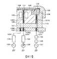
圖1示出作為本實施例的電漿處理裝置,在滿足ECR(Eectron Cyclotron Resonance)條件的磁場中供給微波產生高密度之電漿對被處理晶圓進行處理的電漿處理裝置亦即電漿蝕刻裝置100之例。電漿蝕刻裝置100具備:於內部具有形成電漿的處理室104之真空容器101,及將該真空容器101之上部密閉的介質窗103,在被介質窗103密封的真空容器101之內部形成處理室104。介質窗103由石英等形成。Fig. 1 shows the plasma processing device of this embodiment. Microwaves are supplied in a magnetic field that meets ECR (Eectron Cyclotron Resonance) conditions to generate high-density plasma to process wafers to be processed, that is, plasma. An example of the
在真空容器101之下部配置有排氣口110,與未圖示的真空排氣手段連接。另一方面,在將真空容器101之上部密閉的介質窗103之下方,設置有構成處理室104之天井的圓板狀之噴淋板102。在介質窗103與噴淋板102之間配置有從未圖示的氣體供給手段供給蝕刻處理用之氣體的氣體供給部102a。於噴淋板102形成有將從氣體供給部102a供給的蝕刻處理用之氣體供給至處理室104之複數個氣體導入孔102b。噴淋板102例如由石英等之介質形成。An
又,於真空容器101之外部安裝有,產生供給至真空容器101之內部的微波電力之微波電源106;及將該微波電源106與真空容器101之上部連接,並形成將微波電源106產生的微波搬送至真空容器101的搬送路徑之導波管105。作為微波電源106產生的微波,例如使用頻率2.45GHz之微波。In addition, a
在真空容器101之外部,於真空容器101之上方及在真空容器101之外周設置有介質窗103的部分之周邊分別配置有形成磁場的磁場產生線圈107。磁場產生線圈107連接於磁場產生線圈用電源107a。Outside of the
在真空容器101之內部,於處理室104之下部設置有形成試料台的晶圓載置用電極(第1電極)120。晶圓載置用電極120藉由未圖示的懸架手段被真空容器101之內部支撐。Inside the
晶圓載置用電極120之詳細如圖2所示。晶圓載置用電極120成為由導電性之材料形成的電極基材108、由介質材料形成的絕緣板151、及由導電性之材料形成的接地板152疊層之狀態。電極基材108之上面,周邊部分相對於中央部分低1段,相對於中央部分之上面120a,在低1段的周邊部分形成有面120b。The detail of the
電極基材108與絕緣板151之周圍及電極基材108之面120b,係被由介質材料形成的下部承受器環113、上部承受器環138、及絕緣環139覆蓋。上部承受器環138覆蓋設置於電極基材108之面120b的絕緣環139之上面及側面。The periphery of the
作為形成絕緣板151、下部承受器環113、上部承受器環138及絕緣環139的介質材料,可以使用陶瓷或者石英等。As a dielectric material forming the insulating
電極基材108之上面120a被介質膜140被覆,介質膜140之表面成為載置處理對象亦即試料(半導體晶圓)109的載置面140a。載置面140a,如圖1所示,與噴淋板102及介質窗103呈對向。The
在晶圓載置用電極120之上面120a所形成的介質膜140之內部,如圖3所示,形成有複數個靜電吸附用電極(導電體膜)111。該靜電吸附用電極111,係藉由供電線1261,經由真空容器101之外部所配置的高頻濾波器125連接於直流電源126。供電線1261,在接地板152之部分中通過絕緣管1262之內部,在電極基材108之部分中通過絕緣管1263之內部,而與接地板152及電極基材108絕緣。Inside the
圖3所示構成中,靜電吸附用電極111係經由高頻濾波器125而與一個直流電源126連接的單極之構成,但使用複數個直流電源126對複數個靜電吸附用電極(導電體膜)111供給不同極性之電位的雙極之構成亦可。In the configuration shown in FIG. 3, the
晶圓載置用電極120之電極基材108,係藉由供電線1241,經由匹配器129連接於第1高頻電源124。第1高頻電源124之一端被接地。供電線1241,在接地板152之部分中通過絕緣管1242之內部,而與接地板152被絕緣。The
又,於電極基材108之內部,使為了對電極基材108進行冷卻而流通有從未圖示的冷媒供給手段供給的冷媒之冷媒流路153,在電極基材108之中心軸周圍以螺旋狀形成。於冷媒流路153,從未圖示的冷媒供給手段經由配管154進行冷媒之供給及回收,據此,使冷媒在冷媒流路153之內部循環。In addition, in the inside of the
晶圓載置用電極120之上面120a(電極基材108之上面)之外徑,形成為比載置於載置面140a的試料(半導體晶圓)109之外徑尺寸稍少。其結果,如圖2及圖3所示,將試料(半導體晶圓)109載置於載置面140a的狀態下,試料(半導體晶圓)109之外周部分稍微從載置面140a溢出。The outer diameter of the
又,晶圓載置用電極120之上面120a之周圍之外周部之面120b,形成為比上面120a低一段。於該外周部之面120b,如圖2所示,載置有上部承受器環138與絕緣環139。又,從晶圓載置用電極120之側面遍及其下側之絕緣板151之側面,係被下部承受器環113覆蓋。藉由上部承受器環138與下部承受器環113,將電極基材108之外周面與外周部之面120b覆蓋。In addition, the outer
又,在被上部承受器環138與絕緣環139包圍的區域,絕緣環139在晶圓載置用電極120之外周部之面120b上,以圍繞晶圓載置用電極120之側面的方式被配置。在絕緣環139之上面與內側之面之一部分形成有環電極170。In the area surrounded by the
環電極170之詳細如圖4所示。環電極170,係由在絕緣環139之上面及面對基材電極108之側的內側之面之一部分被形成的薄膜電極171,及覆蓋該薄膜電極171之表面的介質膜172之薄膜構成。薄膜電極171,係藉由供電線1271,如圖2及圖3所示,經由負荷阻抗可變盒130與匹配器128連接於第2高頻電源127。供電線1271,在接地板152之部分中通過絕緣管1272之內部,在電極基材108之部分中通過絕緣管1273之內部,而與接地板152及電極基材108絕緣。The details of the
微波電源106、磁場產生線圈用電源107a、第1高頻電源124、直流電源126、第2高頻電源127分別連接於控制部160,依據記憶於控制部160的程式進行控制。The
這樣的構成中,首先,使用未圖示的試料供給手段,將試料(半導體晶圓)109載置於晶圓載置用電極120之上面120a。接著,在真空容器101密閉的狀態下,藉由控制部160作動未圖示的排氣手段從排氣口110對真空容器101之內部實施真空排氣。In such a configuration, first, a sample (semiconductor wafer) 109 is placed on the
藉由真空排氣使真空容器101之內部到達規定之壓力後,藉由控制部160作動未圖示的氣體供給手段,從氣體供給部102a以規定之流量對介質窗103與噴淋板102之間之空間供給蝕刻處理用之氣體。被供給至介質窗103與噴淋板102之間之空間的蝕刻處理用之氣體,係通過形成於噴淋板102的複數個氣體導入孔102b,流入處理室104。After the inside of the
接著,在被供給有蝕刻處理用之氣體且處理室104之內部維持於規定之壓力之狀態下,藉由控制部160對直流電源126進行控制,經由供電線1261對靜電吸附用電極(導電體膜)111施加直流之電壓。據此,在覆蓋靜電吸附用電極(導電體膜)111的介質膜140之表面(載置面140a)產生靜電氣,試料(半導體晶圓)109被靜電吸附於介質膜140之表面(載置面140a)。Next, in a state where the gas for etching processing is supplied and the inside of the processing chamber 104 is maintained at a predetermined pressure, the
在試料(半導體晶圓)109被靜電吸附於介質膜140之表面(載置面140a)的狀態下,未圖示的氣體供給手段經由控制部160進行控制,在晶圓載置用電極120之表面所形成的介質膜140之表面(載置面140a)與試料(半導體晶圓)109之間,從晶圓載置用電極120之側供給導熱用之氣體(例如氦(He)等)。In a state where the sample (semiconductor wafer) 109 is electrostatically attracted to the surface (mounting
又,藉由控制部160對未圖示的冷媒供給手段進行控制並從配管154使冷媒供給、回收於冷媒流路153中而使冷媒循環於冷媒流路153之內部,據此,使電極基材108冷卻。In addition, the
在該冷卻的電極基材108之上被載置的試料(半導體晶圓)109被靜電吸附於介質膜140之表面,蝕刻處理用之氣體被供給且處理室104之內部成為規定之壓力之狀態下,藉由控制部160對磁場產生線圈用電源107a進行控制,於處理室104之內部產生所要之磁場。進一步,藉由控制部160對微波電源106進行控制使產生微波,使該產生的微波經由導波管105供給至真空容器101之內部。The sample (semiconductor wafer) 109 placed on the cooled
於此,藉由磁場產生線圈用電源107a在處理室104之內部產生的磁場,相對於從微波電源106供給的微波係以滿足ECR條件的方式之強度被形成。據此,供給至處理室104之內部的蝕刻處理用之氣體被激發,生成蝕刻處理用之氣體之高密度的電漿。Here, the magnetic field generated inside the processing chamber 104 by the
另一方面,藉由控制部160對第1高頻電源124進行控制而產生高頻電力,經由匹配器129對電極基材108施加第1高頻電力,據此,相對於電漿116而在電極基材108產生偏壓電位。藉由控制部160對第1高頻電源124進行控制而對產生於電極基材108的偏壓電位進行調整,據此,可以從比較高的密度之電漿116對吸引至電極基材108之側的離子化的蝕刻氣體等之荷電粒子之能量進行控制。On the other hand, the
基於該被控制能量的蝕刻處理用之氣體的荷電粒子與電極基材108之上載置的試料(半導體晶圓)109之表面碰撞。於此,試料(半導體晶圓)109之表面中,藉由與蝕刻處理用之氣體不反應的材料或者難反應的材料形成有遮罩圖案,試料(半導體晶圓)109之表面之未被該遮罩圖案覆蓋的部分被蝕刻。The charged particles of the gas for etching processing based on the controlled energy collide with the surface of the sample (semiconductor wafer) 109 placed on the
蝕刻處理中,導入處理室104之內部的蝕刻處理用之氣體或因為蝕刻處理而產生的反應性生物之粒子,係藉由未圖示的真空排氣手段從排氣口110排出至外部。In the etching process, the gas for etching process introduced into the processing chamber 104 or the particles of reactive organisms generated by the etching process are exhausted from the
又,蝕刻處理中,基於蝕刻處理用之氣體的荷電粒子與表面碰撞後的試料109會產生熱。試料109產生的熱,係藉由在晶圓載置用電極120之表面形成的介質膜140與試料109之間從未圖示的氣體供給手段供給的導熱用之氣體,而從試料109之背面之側,傳導至藉由流過冷媒流路153之內部的冷媒被冷卻了的電極基材108之側。據此,試料109之溫度被調節成為所要之溫度範圍內。於該狀態下,藉由對試料109之表面進行蝕刻處理,而在對試料109不賦予熱損傷之情況下於試料109之表面形成所要之圖案。In addition, during the etching process, the
該試料109之表面之蝕刻處理中,若從電漿116射入試料109之表面的蝕刻處理用之氣體等之荷電粒子之射入量及射入方向遍及試料109之表面全體均勻的話,則試料109之表面大致均勻地被進行處理。In the etching process of the surface of the
但是,實際上,晶圓載置用電極120,為了不使導電性之材料形成的電極基材108暴露於電漿116,因此電極基材108之外周部分被介質材料形成的下部承受器環113、上部承受器環138、絕緣環139披覆,在電極基材108之中央部分與外周部分中,在與電漿116之間形成的鞘區域117之形狀或電場之分布產生差異。However, actually, in order to prevent the
如此般,在電極基材108之中央部分與外周部分藉由鞘區域117之形狀或電場之分布產生差異,據此,在晶圓載置用電極120所載置的試料109之上面,在比較遠離上部承受器環138的中央部與比較接近上部承受器環138的周邊部,在試料109與電漿116之間之鞘區域117所產生的電場變為不一樣,而產生分布。其結果,在試料109之中心部附近與周邊部附近蝕刻處理之條件(荷電粒子之射入量及射入方向)不同而無法進行均勻的蝕刻處理,於試料109之面內,蝕刻處理產生分布。In this way, the shape of the
相對於此,本實施例中,如圖4所示,在電極基材108之周圍所配置的絕緣環139之表面之上面與內側之面之一部分形成有薄膜電極171,從第2高頻電源127經由匹配器128與負荷阻抗可變盒130對薄膜電極171施加高頻電力,據此,而使試料109之表面之中央部與周邊部產生的電場之分布之差異盡可能減小。In contrast to this, in this embodiment, as shown in FIG. 4, a thin-
第2高頻電源127係和對電極基材108施加高頻電力的第1高頻電源124為不同的電源,對薄膜電極171施加和施加於電極基材108的高頻電力為獨立的電力。The second high-
於此,於專利文獻2記載有,從高頻電源對表面被由介質形成的承受器環披覆的導體環施加高頻電力,據此而對晶圓之外周部分或者外周緣部有效地貢獻高頻。Herein, Patent Document 2 describes that high-frequency power is applied from a high-frequency power supply to a conductor ring whose surface is covered by a susceptor ring formed of a dielectric, thereby effectively contributing to the outer periphery of the wafer or the outer periphery. high frequency.
但是,導體環與金屬製之基材之間會產生容量耦合。因為該導體環與基材之間之容量耦合而產生的耦合電容C,會受到介於其間的絕緣體之介電常數及厚度而變化,導體環被賦予某一程度之厚度而形成,因此導體環在高度方向之位置被限定之情況下,介於其間的絕緣體之厚度不得不被削薄和導體環之厚度相當的量。因此,在減少導體環與基材之間之耦合電容C上受到源自於絕緣體之厚度的限制。However, capacitive coupling occurs between the conductor ring and the metal base material. Because the coupling capacitance C generated by the capacitive coupling between the conductor ring and the substrate will be changed by the dielectric constant and thickness of the insulator between them, the conductor ring is formed by giving a certain degree of thickness, so the conductor ring When the position in the height direction is limited, the thickness of the insulator between them has to be reduced by an amount equivalent to the thickness of the conductor ring. Therefore, the reduction of the coupling capacitance C between the conductor ring and the substrate is limited by the thickness of the insulator.
其結果,專利文獻2之構成中,對導體環與電極亦即基材從不同之高頻電源獨立施加高頻電力之情況下,施加於導體環的比較小的高頻電力,因為導體環與基材之間之容量耦合而受到施加於電極亦即基材的比較大的高頻電力之影響,形成於導體環之周圍的電場之控制性降低,有可能無法獲得所要之電場分布。As a result, in the structure of Patent Document 2, when high-frequency power is independently applied from different high-frequency power supplies to the conductor ring and the electrode, that is, the substrate, the relatively small high-frequency power applied to the conductor ring is because the conductor ring and the The capacitance coupling between the substrates is affected by the relatively large high-frequency power applied to the electrode, that is, the substrate, and the controllability of the electric field formed around the conductor loop is reduced, and the desired electric field distribution may not be obtained.
相對於此,本實施例中,如圖4所示,和專利文獻2記載之導體環相當的功能,係由在介質形成的絕緣環139之表面所形成的環電極170來實現。亦即,本實施例中設為,在絕緣環139之表面,作為環電極170而形成薄膜電極171並將其表面以介質膜172披覆之構成,據此,則相對於專利文獻2記載的構成,本實施例之構成中,與電極基材108之外周部之面120b間之間隔可以增大和專利文獻2之導體環之厚度相當的部分之量。On the other hand, in this embodiment, as shown in FIG. 4, the function equivalent to the conductor ring described in Patent Document 2 is realized by the
據此,本實施例中的薄膜電極171與電極基材108之外周部之面120b之間之耦合電容C,相較於專利文獻2記載的構成中的導體環與基材之相當於本實施例中的面120b的部分之間之耦合電容可以減小。Accordingly, the coupling capacitance C between the thin-
其結果,本實施例中,從各自之高頻電源對薄膜電極171與電極基材108獨立施加高頻電力之情況下,施加於薄膜電極171的比較小的高頻電力中,受到基於薄膜電極171與電極基材108之間之容量耦合而施加於電極基材108的比較大的高頻電力之影響可以減小,因此形成於薄膜電極171之周圍的電場可以穩定地進行控制。As a result, in this embodiment, when high-frequency power is independently applied to the thin-
又,藉由介質膜172披覆薄膜電極171之表面,於處理室104之內部產生電漿,從第1高頻電源127對薄膜電極171施加第2高頻電力時,可以防止薄膜電極171中產生異常放電,可以防止試料109之周邊部中的鞘區域之形狀或鞘區域之電場之分布產生紊亂。In addition, by covering the surface of the thin-
薄膜電極171,係於絕緣環139之表面熔射鎢(W)而形成鎢之薄膜。又,介質膜172係以披覆絕緣環139之表面之熔射有鎢之薄膜之部分的方式熔射氧化鋁而藉由氧化鋁之薄膜來形成。The
又,將絕緣環139之上面與在該上面連接的內側之側面所交接的部分173,如圖4所示設為去角部的帶圓弧的R形狀。將薄膜電極171形成於,包含該去角部而設為帶圓弧的R形狀之部分且在絕緣環139之上面與該上面連接的內側之側面,據此,對薄膜電極171施加高頻電力時,可以防止電場集中於該去角部而設為R形狀之部分。如此般藉由防止電場之集中,對於試料109之周邊部中的鞘區域之形狀或鞘區域之電場之分布不會造成影響,或者可以減少影響。In addition, the
藉由控制部160控制第2高頻電源127,經由負荷阻抗可變盒130與匹配器128藉由供電線1271對如此般形成的環電極170之薄膜電極171施加第2高頻電力。同時,從第1高頻電源124經由匹配器129藉由供電線1241對電極基材108施加第1高頻電力。The second high-
於此,藉由薄膜電極171與電極基材108之外周部之面120b之間之容量耦合所產生的耦合電容C,係和與電極基材108之外周部之面120b對向的薄膜電極171之面積呈比例,且和電極基材108之外周部之面120b與薄膜電極171之間之間隔呈反比例。Here, the coupling capacitance C generated by the capacitive coupling between the
圖4所示環電極170之構成中,於絕緣環139之左側側面1391之上部亦形成有薄膜電極171,該部分中薄膜電極171與電極基材108之側面對置之部分之面積,相比於與電極基材108之外周部之面120b對置之部分之面積為充分小,因此薄膜電極171與電極基材108之間所形成的容量耦合,可以視為由薄膜電極171與電極基材108之外周部之面120b之間之容量耦合引起的耦合電容C所支配。In the structure of the
依據這樣的構成,藉由控制部160對第2高頻電源127進行控制,如圖5所示,在晶圓載置用電極120之外周部附近中,在從試料109之周邊部遍及上部承受器環138的部分之電漿116區域與試料109之間所形成的鞘區域117,可以減少鞘區域117受到第1高頻電力之影響而導致的形狀隨時間的變化,可以穩定地形成。According to this configuration, the second high-
又,薄膜電極171係形成於包含絕緣環139之去角部之部分在內的絕緣環139之上面與內側之面,因此不會發生電場集中,可以減少晶圓載置用電極120載置的試料109之外周部附近電場之失真。其結果,試料109之上面所形成的電漿116之鞘區域117之電場分布,從試料109之中心部分至周邊部分可以設為大致均勻。In addition, the thin-
據此,從電漿116射入自試料109之中心部分至周邊部分的荷電粒子之射入方向可以成為大致同一方向,試料109上被蝕刻形成的圖案之形狀在試料109中心部附近與周邊部附近產生之偏差可以被抑制。According to this, the charging direction of the charged particles injected from the
又,藉由消除電場之集中,不會發生上部承受器環138之局部性消耗,可以延長上部承受器環138之壽命。其結果,可以減少上部承受器環138之交換之頻度,可以提升電漿蝕刻裝置100之裝置運轉率。In addition, by eliminating the concentration of the electric field, local consumption of the
上述實施例中說明,使環電極170,在由介質形成的絕緣環139之表面,熔射鎢(W)而形成導體薄膜,並於其上熔射氧化鋁而形成介質膜172的構成,但作為熔射鎢(W)而形成的導體薄膜之替換,可以使用沿著絕緣環139之表面成形的薄的金屬之板,於其表面熔射氧化鋁而成者。In the above embodiment, it is described that the
依據本實施例,至晶圓外周部為止能夠均勻地實施電漿處理,因此在晶圓之面內可以均勻地實施處理,可以實現半導體素子之良品率提升。According to this embodiment, the plasma processing can be uniformly performed up to the outer periphery of the wafer, so the processing can be uniformly performed on the surface of the wafer, and the yield of semiconductor elements can be improved.
又,在配置於晶圓載置用電極120之電極基材108之外周部而直接暴露於電漿的上部承受器環138中,可以防止電場之集中,因此上部承受器環138之壽命可以延長。In addition, in the
以上,依據實施例具體說明本發明者完成的發明,但本發明不限定於上述實施例,在不脫離其要旨範圍內可以進行各種變更。例如上述實施例係為了容易理解本發明而詳細說明者,但未必限定於具備說明的全部構成。又,針對實施例之構成之一部分,可以進行公知之構成之追加・削除・置換。In the above, the invention completed by the inventors was specifically described based on the embodiments, but the present invention is not limited to the above-mentioned embodiments, and various changes can be made without departing from the scope of the gist. For example, the above-mentioned embodiments are described in detail in order to facilitate the understanding of the present invention, but are not necessarily limited to having all the configurations described. In addition, it is possible to add, delete, or replace a part of the configuration of the embodiment with a known configuration.
100:電漿蝕刻裝置101:真空容器102:噴淋板102a:氣體供給部103:介質窗104:處理室106:微波電源107:磁場產生線圈107a:磁場產生線圈用電源108:電極基材109:試料110:排氣口111:靜電吸附用電極113:下部承受器環120:晶圓載置用電極124:第1高頻電源127:第2高頻電源138:上部承受器環139:絕緣環140:介質膜160:控制部170:環電極171:薄膜電極172:介質膜100: Plasma etching device101: vacuum container102:
[圖1]表示本發明之實施例的電漿處理裝置之概略構成的方塊圖。[圖2]表示本發明之實施例的電漿處理裝置之晶圓載置用電極之構成的剖面圖。[圖3]經由本發明之實施例的電漿處理裝置之晶圓載置用電極之周邊部之詳細構成的剖面圖。[圖4]經由本發明之實施例的電漿處理裝置之晶圓載置用電極之絕緣環與環電極之構成的剖面圖。[圖5]經由本發明之實施例的電漿處理裝置之晶圓載置用電極之周邊部中的電漿鞘之狀態的晶圓載置用電極之周邊部之剖面圖。[Fig. 1] A block diagram showing the schematic configuration of a plasma processing apparatus according to an embodiment of the present invention.[FIG. 2] A cross-sectional view showing the structure of a wafer mounting electrode of a plasma processing apparatus according to an embodiment of the present invention.[Fig. 3] A cross-sectional view showing the detailed structure of the peripheral portion of the electrode for placing a wafer in the plasma processing apparatus according to the embodiment of the present invention.[FIG. 4] A cross-sectional view of the structure of the insulating ring and the ring electrode of the wafer mounting electrode of the plasma processing apparatus according to the embodiment of the present invention.[FIG. 5] A cross-sectional view of the peripheral portion of the wafer mounting electrode in the state of the plasma sheath in the peripheral portion of the wafer mounting electrode of the plasma processing apparatus of the embodiment of the present invention.
100:電漿蝕刻裝置100: Plasma etching device
101:真空容器101: vacuum container
102:噴淋板102: spray board
102a:氣體供給部102a: Gas supply unit
102b:氣體導入孔102b: Gas inlet hole
103:介質窗103: Medium window
105:導波管105: Stillpipe
106:微波電源106: Microwave power supply
107:磁場產生線圈107: Magnetic field generating coil
107a:磁場產生線圈用電源107a: Power supply for magnetic field generating coil
108:電極基材108: Electrode base material
109:試料109: Sample
110:排氣口110: exhaust port
113:下部承受器環113: Lower susceptor ring
116:電漿116: Plasma
117:鞘區域117: Sheath area
120:晶圓載置用電極120: Electrode for wafer placement
124:第1高頻電源124: The first high frequency power supply
125:高頻濾波器125: high frequency filter
126:直流電源126: DC power supply
127:第2高頻電源127: The second high frequency power supply
128、129:匹配器128, 129: matcher
130:負荷阻抗可變盒130: Load impedance variable box
138:上部承受器環138: Upper susceptor ring
139:絕緣環139: Insulation ring
140:介質膜140: Dielectric film
151:絕緣板151: Insulation board
152:接地板152: Ground Plate
160:控制部160: Control Department
Claims (8)
Translated fromChineseApplications Claiming Priority (2)
| Application Number | Priority Date | Filing Date | Title |
|---|---|---|---|
| JP2018-166773 | 2018-09-06 | ||
| JP2018166773AJP7140610B2 (en) | 2018-09-06 | 2018-09-06 | Plasma processing equipment |
Publications (2)
| Publication Number | Publication Date |
|---|---|
| TW202011478A TW202011478A (en) | 2020-03-16 |
| TWI734185Btrue TWI734185B (en) | 2021-07-21 |
Family
ID=69718841
Family Applications (2)
| Application Number | Title | Priority Date | Filing Date |
|---|---|---|---|
| TW108131630ATWI734185B (en) | 2018-09-06 | 2019-09-03 | Plasma processing apparatus |
| TW110122320ATWI850569B (en) | 2018-09-06 | 2019-09-03 | Plasma processing apparatus |
Family Applications After (1)
| Application Number | Title | Priority Date | Filing Date |
|---|---|---|---|
| TW110122320ATWI850569B (en) | 2018-09-06 | 2019-09-03 | Plasma processing apparatus |
Country Status (5)
| Country | Link |
|---|---|
| US (1) | US20200083026A1 (en) |
| JP (2) | JP7140610B2 (en) |
| KR (1) | KR102218686B1 (en) |
| CN (1) | CN110880443B (en) |
| TW (2) | TWI734185B (en) |
Families Citing this family (9)
| Publication number | Priority date | Publication date | Assignee | Title |
|---|---|---|---|---|
| WO2020255319A1 (en)* | 2019-06-20 | 2020-12-24 | 株式会社日立ハイテク | Plasma processing device and plasma processing method |
| JP7454961B2 (en)* | 2020-03-05 | 2024-03-25 | 東京エレクトロン株式会社 | plasma processing equipment |
| JP7265287B2 (en) | 2020-03-06 | 2023-04-26 | シー アンド エム ロボティクス カンパニー リミテッド | Friction wave reducer |
| JP2022049504A (en)* | 2020-09-16 | 2022-03-29 | 株式会社東芝 | Dielectric barrier discharge device |
| KR102687065B1 (en) | 2020-12-29 | 2024-07-24 | 세메스 주식회사 | Substrate treating apparatus and susbstrate treating method |
| KR102851225B1 (en)* | 2021-01-19 | 2025-08-27 | 에스케이하이닉스 주식회사 | Substrate Treatment Apparatus Having an Intermediate Electrode |
| WO2022201351A1 (en)* | 2021-03-24 | 2022-09-29 | 株式会社日立ハイテク | Plasma treatment device and plasma treatment method |
| WO2024215015A2 (en)* | 2023-04-14 | 2024-10-17 | 주식회사 플라즈맵 | Plasma processing container and plasma processing apparatus |
| WO2024215016A1 (en)* | 2023-04-14 | 2024-10-17 | 주식회사 플라즈맵 | Plasma treatment vessel and plasma treatment device |
Citations (2)
| Publication number | Priority date | Publication date | Assignee | Title |
|---|---|---|---|---|
| CN102163530A (en)* | 2007-08-31 | 2011-08-24 | 东京毅力科创株式会社 | Plasma processing apparatus |
| US8878434B2 (en)* | 2009-10-27 | 2014-11-04 | Covidien Lp | Inductively-coupled plasma device |
Family Cites Families (18)
| Publication number | Priority date | Publication date | Assignee | Title |
|---|---|---|---|---|
| JPH05183043A (en)* | 1992-01-07 | 1993-07-23 | Ryoden Semiconductor Syst Eng Kk | Electrostatic adsorption device and electrostatic adsorption method |
| JP2001034372A (en)* | 1999-07-23 | 2001-02-09 | Alpine Electronics Inc | Data communication system |
| JP5165825B2 (en)* | 2000-01-10 | 2013-03-21 | 東京エレクトロン株式会社 | Divided electrode assembly and plasma processing method. |
| KR100502268B1 (en)* | 2000-03-01 | 2005-07-22 | 가부시끼가이샤 히다치 세이사꾸쇼 | Plasma processing apparatus and method |
| JP3606198B2 (en)* | 2000-12-14 | 2005-01-05 | 株式会社日立製作所 | Plasma processing equipment |
| CN100418187C (en)* | 2003-02-07 | 2008-09-10 | 东京毅力科创株式会社 | Plasma processing apparatus, annular component and plasma processing method |
| JP4846190B2 (en)* | 2003-05-16 | 2011-12-28 | 東京エレクトロン株式会社 | Plasma processing apparatus and control method thereof |
| JP4365766B2 (en)* | 2004-10-26 | 2009-11-18 | 京セラ株式会社 | Wafer support member and semiconductor manufacturing apparatus using the same |
| US20080289766A1 (en)* | 2007-05-22 | 2008-11-27 | Samsung Austin Semiconductor Lp | Hot edge ring apparatus and method for increased etch rate uniformity and reduced polymer buildup |
| JP5357639B2 (en)* | 2009-06-24 | 2013-12-04 | 株式会社日立ハイテクノロジーズ | Plasma processing apparatus and plasma processing method |
| JP5970268B2 (en) | 2012-07-06 | 2016-08-17 | 株式会社日立ハイテクノロジーズ | Plasma processing apparatus and processing method |
| CN103715049B (en)* | 2012-09-29 | 2016-05-04 | 中微半导体设备(上海)有限公司 | The method of plasma processing apparatus and adjusting substrate edge region processing procedure speed |
| JP6452449B2 (en)* | 2015-01-06 | 2019-01-16 | 東京エレクトロン株式会社 | Mounting table and substrate processing apparatus |
| JP6539113B2 (en) | 2015-05-28 | 2019-07-03 | 株式会社日立ハイテクノロジーズ | Plasma processing apparatus and plasma processing method |
| US10163610B2 (en)* | 2015-07-13 | 2018-12-25 | Lam Research Corporation | Extreme edge sheath and wafer profile tuning through edge-localized ion trajectory control and plasma operation |
| CN108074787A (en)* | 2016-11-10 | 2018-05-25 | 北京北方华创微电子装备有限公司 | Lower electrode arrangement and semiconductor processing equipment |
| SG11201908264QA (en)* | 2017-07-24 | 2019-10-30 | Lam Res Corp | Moveable edge ring designs |
| CN118380371A (en)* | 2017-11-21 | 2024-07-23 | 朗姆研究公司 | Bottom edge ring and middle edge ring |
- 2018
- 2018-09-06JPJP2018166773Apatent/JP7140610B2/enactiveActive
- 2019
- 2019-08-09KRKR1020190097182Apatent/KR102218686B1/enactiveActive
- 2019-08-13CNCN201910746777.5Apatent/CN110880443B/enactiveActive
- 2019-09-03TWTW108131630Apatent/TWI734185B/enactive
- 2019-09-03TWTW110122320Apatent/TWI850569B/enactive
- 2019-09-05USUS16/561,785patent/US20200083026A1/ennot_activeAbandoned
- 2022
- 2022-09-08JPJP2022143028Apatent/JP7364758B2/enactiveActive
Patent Citations (3)
| Publication number | Priority date | Publication date | Assignee | Title |
|---|---|---|---|---|
| CN102163530A (en)* | 2007-08-31 | 2011-08-24 | 东京毅力科创株式会社 | Plasma processing apparatus |
| CN102163530B (en) | 2007-08-31 | 2014-06-04 | 东京毅力科创株式会社 | Plasma processing apparatus |
| US8878434B2 (en)* | 2009-10-27 | 2014-11-04 | Covidien Lp | Inductively-coupled plasma device |
Also Published As
| Publication number | Publication date |
|---|---|
| CN110880443B (en) | 2022-07-08 |
| US20200083026A1 (en) | 2020-03-12 |
| TW202011478A (en) | 2020-03-16 |
| CN110880443A (en) | 2020-03-13 |
| JP2022179495A (en) | 2022-12-02 |
| KR102218686B1 (en) | 2021-02-19 |
| JP7140610B2 (en) | 2022-09-21 |
| TWI850569B (en) | 2024-08-01 |
| JP7364758B2 (en) | 2023-10-18 |
| JP2020043100A (en) | 2020-03-19 |
| TW202137393A (en) | 2021-10-01 |
| KR20200028288A (en) | 2020-03-16 |
Similar Documents
| Publication | Publication Date | Title |
|---|---|---|
| TWI734185B (en) | Plasma processing apparatus | |
| KR100900585B1 (en) | Focus ring and plasma processing apparatus | |
| KR100886272B1 (en) | Plasma processing equipment | |
| KR100274757B1 (en) | Plasma treatment apparatus and plasma treatment method | |
| WO2019032787A1 (en) | A distributed electrode array for plasma processing | |
| KR102432857B1 (en) | plasma processing apparatus and manufacturing method of semiconductor device using the same | |
| JP3150058B2 (en) | Plasma processing apparatus and plasma processing method | |
| US20150243486A1 (en) | Plasma processing apparatus | |
| JP2001257199A (en) | Plasma processing method and device thereof | |
| KR20010087219A (en) | Plasma processing apparatus and method | |
| TWI873545B (en) | Plasma processing apparatus | |
| TWI843988B (en) | Plasma treatment device and plasma treatment method | |
| JP2019121748A (en) | Plasma processing apparatus | |
| TWI723406B (en) | Plasma processing device | |
| JP3814176B2 (en) | Plasma processing equipment | |
| TW201939604A (en) | Plasma processing apparatus | |
| JP3197739B2 (en) | Plasma processing equipment | |
| JP2001319920A (en) | Plasma processing apparatus and processing method | |
| US12444581B2 (en) | Plasma processing apparatus | |
| US20220157576A1 (en) | Plasma processing apparatus | |
| KR20240114600A (en) | substrate processing apparatus |