TWI733042B - Multi-frequency antenna device - Google Patents
Multi-frequency antenna deviceDownload PDFInfo
- Publication number
- TWI733042B TWI733042BTW107126705ATW107126705ATWI733042BTW I733042 BTWI733042 BTW I733042BTW 107126705 ATW107126705 ATW 107126705ATW 107126705 ATW107126705 ATW 107126705ATW I733042 BTWI733042 BTW I733042B
- Authority
- TW
- Taiwan
- Prior art keywords
- electrode layer
- antenna device
- hole
- base
- insulating
- Prior art date
Links
- 239000000758substrateSubstances0.000claimsabstractdescription53
- 239000007769metal materialSubstances0.000claimsdescription7
- 239000011810insulating materialSubstances0.000claimsdescription5
- 238000009413insulationMethods0.000claims1
- 239000010410layerSubstances0.000description186
- 238000010586diagramMethods0.000description15
- 239000011229interlayerSubstances0.000description4
- 238000004519manufacturing processMethods0.000description3
- 230000005540biological transmissionEffects0.000description1
- 239000004020conductorSubstances0.000description1
- 230000010354integrationEffects0.000description1
- 238000000034methodMethods0.000description1
- 235000015096spiritNutrition0.000description1
Images


Classifications
- H—ELECTRICITY
- H01—ELECTRIC ELEMENTS
- H01Q—ANTENNAS, i.e. RADIO AERIALS
- H01Q1/00—Details of, or arrangements associated with, antennas
- H01Q1/42—Housings not intimately mechanically associated with radiating elements, e.g. radome
- H—ELECTRICITY
- H01—ELECTRIC ELEMENTS
- H01Q—ANTENNAS, i.e. RADIO AERIALS
- H01Q5/00—Arrangements for simultaneous operation of antennas on two or more different wavebands, e.g. dual-band or multi-band arrangements
- H01Q5/30—Arrangements for providing operation on different wavebands
- H01Q5/307—Individual or coupled radiating elements, each element being fed in an unspecified way
- H01Q5/342—Individual or coupled radiating elements, each element being fed in an unspecified way for different propagation modes
- H01Q5/357—Individual or coupled radiating elements, each element being fed in an unspecified way for different propagation modes using a single feed point
- H01Q5/364—Creating multiple current paths
- H01Q5/371—Branching current paths
- H—ELECTRICITY
- H01—ELECTRIC ELEMENTS
- H01Q—ANTENNAS, i.e. RADIO AERIALS
- H01Q1/00—Details of, or arrangements associated with, antennas
- H01Q1/12—Supports; Mounting means
- H01Q1/22—Supports; Mounting means by structural association with other equipment or articles
- H01Q1/24—Supports; Mounting means by structural association with other equipment or articles with receiving set
- H—ELECTRICITY
- H01—ELECTRIC ELEMENTS
- H01Q—ANTENNAS, i.e. RADIO AERIALS
- H01Q1/00—Details of, or arrangements associated with, antennas
- H01Q1/36—Structural form of radiating elements, e.g. cone, spiral, umbrella; Particular materials used therewith
- H01Q1/38—Structural form of radiating elements, e.g. cone, spiral, umbrella; Particular materials used therewith formed by a conductive layer on an insulating support
- H—ELECTRICITY
- H01—ELECTRIC ELEMENTS
- H01Q—ANTENNAS, i.e. RADIO AERIALS
- H01Q13/00—Waveguide horns or mouths; Slot antennas; Leaky-waveguide antennas; Equivalent structures causing radiation along the transmission path of a guided wave
- H01Q13/10—Resonant slot antennas
- H01Q13/106—Microstrip slot antennas
- H—ELECTRICITY
- H01—ELECTRIC ELEMENTS
- H01Q—ANTENNAS, i.e. RADIO AERIALS
- H01Q21/00—Antenna arrays or systems
- H01Q21/06—Arrays of individually energised antenna units similarly polarised and spaced apart
- H01Q21/061—Two dimensional planar arrays
- H01Q21/065—Patch antenna array
- H—ELECTRICITY
- H01—ELECTRIC ELEMENTS
- H01Q—ANTENNAS, i.e. RADIO AERIALS
- H01Q5/00—Arrangements for simultaneous operation of antennas on two or more different wavebands, e.g. dual-band or multi-band arrangements
- H01Q5/30—Arrangements for providing operation on different wavebands
- H01Q5/378—Combination of fed elements with parasitic elements
- H—ELECTRICITY
- H01—ELECTRIC ELEMENTS
- H01Q—ANTENNAS, i.e. RADIO AERIALS
- H01Q5/00—Arrangements for simultaneous operation of antennas on two or more different wavebands, e.g. dual-band or multi-band arrangements
- H01Q5/50—Feeding or matching arrangements for broad-band or multi-band operation
- H—ELECTRICITY
- H01—ELECTRIC ELEMENTS
- H01Q—ANTENNAS, i.e. RADIO AERIALS
- H01Q9/00—Electrically-short antennas having dimensions not more than twice the operating wavelength and consisting of conductive active radiating elements
- H01Q9/04—Resonant antennas
- H01Q9/0407—Substantially flat resonant element parallel to ground plane, e.g. patch antenna
- H01Q9/0414—Substantially flat resonant element parallel to ground plane, e.g. patch antenna in a stacked or folded configuration
Landscapes
- Waveguide Aerials (AREA)
- Details Of Aerials (AREA)
- Variable-Direction Aerials And Aerial Arrays (AREA)
Abstract
Description
Translated fromChinese本發明是有關於一種多頻天線裝置,主要於設置電極層的絕緣基體上設置至少一凹槽,藉此以改變介於第二電極層與第三電極層之間的夾層的有效介電係數,並達到調整電極層所產生的共振頻率的目的。The present invention relates to a multi-frequency antenna device, which is mainly provided with at least one groove on an insulating substrate on which an electrode layer is provided, so as to change the effective dielectric constant of the interlayer between the second electrode layer and the third electrode layer , And achieve the purpose of adjusting the resonance frequency generated by the electrode layer.
相較於一般的天線,微帶天線結構能夠用以製作圓極化天線,具有平面結構、可大量生產及方便整合在主動元件或電路板…等優點,因而被大量的應用在各種無線傳輸裝置上,例如全球定位系統GPS(Global Positioning System)或無線射頻辨識(RFID)。Compared with general antennas, the microstrip antenna structure can be used to make circularly polarized antennas. It has the advantages of planar structure, mass production, and easy integration in active components or circuit boards, etc., so it is widely used in various wireless transmission devices. Above, such as Global Positioning System GPS (Global Positioning System) or Radio Frequency Identification (RFID).
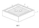
請參閱圖1,為習用微帶天線之立體透視圖。如圖所示,習用之微帶天線10包括一絕緣基體11、一第一導電層13、一第二導電層15及一導電元件171,其中第一導電層13位於絕緣基體11的上表面,而第二導電層15則位於絕緣基體11的下表面。導電元件171貫穿絕緣基體11、第一導電層13及第二導電層15,並電性連接第一導電層13。Please refer to Figure 1, which is a perspective view of a conventional microstrip antenna. As shown in the figure, the
設置在絕緣基體11上表面的第一導電層13可作為微帶天線10的幅射體,而設置在絕緣基體11下表面的第二導電層15則為接地面。在透過微帶天線10進行無線射頻訊號的接收時,無線射頻訊號會由第一導電層13經由導電元件171輸入,而在進行無線射頻訊號的發射時,訊號則會經由導電元件171傳送至第一導電層13,並經由第一導電層13發射無線訊號。The first
微帶天線10能夠接收或發射之無線訊號的頻率與第一導電層13的長度及寬度相關,此外亦與絕緣基體11的介電係數相關。若欲製作共振頻率較低的微帶天線10,便需要增加第一導電層13的長度或寬度,如此一來將會增加微帶天線10的體積及製作成本。當然亦可選用介電係數較高的絕緣基體11製作微帶天線10,以達到降低微帶天線10之共振頻率的目的,此一方式雖然可避免增加微帶天線10的體積,但同樣會增加微帶天線10的製作成本。而當絕緣基體的尺寸與介電係數選定之後,基本上,在該微帶天線上能夠形成的共振頻率就已經固定,所以,在一個絕緣基體上製作具有兩個共振頻率的微帶天線時,不容易同時精確且有效的調整兩個共振頻率。The frequency of the wireless signal that the
本發明提出一種多頻天線裝置,主要於絕緣基體的上表面設置第一電極層及第二電極層,並於絕緣基體的下表面設置第三電極層,其中第二電極層位於第一電極層的外圍,且和第一電極層沒有相互接觸。絕緣基體的側表面及/或下表面上可設置至少一凹槽,該凹槽與第二電極層部分或全部重疊。該第一電極層與該第二電極層可分別形成不同的共振頻率,而透過凹槽的設置可改變介於第二電極層與第三電極層之間的夾層的有效介電係數,藉此以調整第二電極層所產生的共振頻率。The present invention provides a multi-frequency antenna device, which is mainly provided with a first electrode layer and a second electrode layer on the upper surface of an insulating substrate, and a third electrode layer is provided on the lower surface of the insulating substrate, wherein the second electrode layer is located on the first electrode layer And the first electrode layer is not in contact with each other. At least one groove may be provided on the side surface and/or the lower surface of the insulating base, and the groove partially or completely overlaps the second electrode layer. The first electrode layer and the second electrode layer can respectively form different resonance frequencies, and the arrangement of the groove can change the effective dielectric constant of the interlayer between the second electrode layer and the third electrode layer, thereby To adjust the resonance frequency generated by the second electrode layer.
本發明提出一種多頻天線裝置,主要於絕緣基體的側表面及/或下表面及/或絕緣基體的內部設置至少一凹槽,並使得凹槽在第一表面的投影與絕緣基體上的部分電極層重疊。此外亦可調整凹槽在第一表面的投影與電極層的重疊面積及/或調整凹槽的縱向深度及/或凹槽的設置位置,以調整電極層所產生的共振頻率。The present invention provides a multi-frequency antenna device, which is mainly provided with at least one groove on the side surface and/or lower surface of an insulating base and/or inside the insulating base, so that the projection of the groove on the first surface and the part on the insulating base The electrode layers overlap. In addition, the overlap area of the projection of the groove on the first surface and the electrode layer and/or the longitudinal depth of the groove and/or the arrangement position of the groove can be adjusted to adjust the resonance frequency generated by the electrode layer.
本發明提出一種多頻天線裝置,包括:一絕緣基體,包括至少一第一通孔、一第一表面、一第二表面及至少一側表面,其中第一表面與第二表面為隔著絕緣基體相對的兩個表面,且第一表面經由側表面連接第二表面,而第一通孔穿透絕緣基體;至少一第一電極層,建置於絕緣基體的第一表面;至少一第二電極層,設置在絕緣基體的第一表面,並位於第一電極層的外圍,且與第一電極層沒有相互接觸;至少一第三電極層,建置於絕緣基體的第二表面;至少一導電元件,穿過第一通孔並電性連接第一電極層,且不接觸第三電極層;及至少一凹槽,設置於絕緣基體的側表面或/及第二表面,其中凹槽在第一表面的投影與第二電極層完全或部分重疊,其中第一電極層用以產生一第一共振頻率,而第二電極層則用以產生一第二共振頻率,且第一共振頻率高於第二共振頻率。The present invention provides a multi-band antenna device, including: an insulating base, including at least one first through hole, a first surface, a second surface, and at least one side surface, wherein the first surface and the second surface are insulated from each other. Two opposite surfaces of the base, and the first surface is connected to the second surface through the side surface, and the first through hole penetrates the insulating base; at least one first electrode layer is built on the first surface of the insulating base; at least one second The electrode layer is arranged on the first surface of the insulating base and located at the periphery of the first electrode layer and is not in contact with the first electrode layer; at least one third electrode layer is built on the second surface of the insulating base; at least one The conductive element passes through the first through hole and is electrically connected to the first electrode layer without contacting the third electrode layer; and at least one groove is provided on the side surface or/and the second surface of the insulating base, wherein the groove is The projection of the first surface is completely or partially overlapped with the second electrode layer, where the first electrode layer is used to generate a first resonance frequency, and the second electrode layer is used to generate a second resonance frequency, and the first resonance frequency is high At the second resonance frequency.
本發明提出另一種多頻天線裝置,包括:一絕緣基體,包括至少一第一通孔、一第一表面及一第二表面,其中第一表面與第二表面為隔著絕緣基體相對的兩個表面,而第一通孔穿透絕緣基體;至少一第一電極層,建置於絕緣基體的第一表面;至少一第二電極層,設置在絕緣基體的第一表面,並位於第一電極層的外圍,且和第一電極層沒有相互接觸;至少一第三電極層,建置於絕緣基體的第二表面;一承載基體,包括至少一第二通孔、一第三表面、一第四表面及至少一側表面,其中第三表面與第四表面為隔著承載基體相對的兩個表面,且第三表面經由側表面連接第四表面,而第二通孔穿透承載基體,其中第三表面之全部或部分區域附著於絕緣基體的第二表面,且第二通孔連通絕緣基體的第一通孔;至少一導電元件,穿過第一通孔及第二通孔並電性連接第一電極層,且不接觸第三電極層;及至少一凹槽,設置於絕緣基體的側表面或/及第二表面,或/及承載基體的側表面或/及第三表面或/及第四表面,其中凹槽在第一表面的投影與第二電極層完全或部分重疊,其中第一電極層用以產生一第一共振頻率,而第二電極層則用以產生一第二共振頻率,且第一共振頻率高於第二共振頻率。The present invention provides another multi-band antenna device, including: an insulating substrate, including at least one first through hole, a first surface, and a second surface, wherein the first surface and the second surface are two opposite sides of the insulating substrate. The first through hole penetrates the insulating substrate; at least one first electrode layer is built on the first surface of the insulating substrate; at least one second electrode layer is provided on the first surface of the insulating substrate and is located on the first surface The periphery of the electrode layer and the first electrode layer are not in contact with each other; at least one third electrode layer is built on the second surface of the insulating substrate; a carrier substrate includes at least one second through hole, a third surface, and The fourth surface and at least one side surface, wherein the third surface and the fourth surface are two surfaces opposite to each other through the supporting base, and the third surface is connected to the fourth surface via the side surface, and the second through hole penetrates the supporting base, Wherein all or part of the third surface is attached to the second surface of the insulating base, and the second through hole is connected to the first through hole of the insulating base; at least one conductive element passes through the first through hole and the second through hole and is electrically connected Is connected to the first electrode layer and does not contact the third electrode layer; and at least one groove is provided on the side surface or/and the second surface of the insulating substrate, or/and the side surface of the supporting substrate or/and the third surface or / And the fourth surface, where the projection of the groove on the first surface completely or partially overlaps the second electrode layer, where the first electrode layer is used to generate a first resonance frequency, and the second electrode layer is used to generate a first Two resonance frequencies, and the first resonance frequency is higher than the second resonance frequency.
本發明還提供一種多頻天線裝置,包括:一絕緣基體,包括至少一第一通孔、一第一表面、一第二表面及至少一側表面,其中第一表面與第二表面為隔著絕緣基體相對的兩個表面,且第一表面經由側表面連接第二表面,而第一通孔穿透絕緣基體;至少一第一電極層,建置於絕緣基體的第一表面;至少一第二電極層,設置在絕緣基體的第一表面,並位於第一電極層的外圍;一承載基體,包括至少一第二通孔、一第三表面、一第四表面及至少一側表面,其中第三表面與第四表面為隔著承載基體相對的兩個表面,且第三表面經由側表面連接第四表面,而第二通孔穿透承載基體,其中第三表面之全部或部分區域附著於絕緣基體的第二表面,且第二通孔連通絕緣基體的第一通孔;至少一導電元件,穿過第一通孔及第二通孔並電性連接第一電極層;及至少一凹槽,設置於絕緣基體的側表面或/及第二表面,或/及承載基體的側表面或/及第三表面或/及第四表面,其中凹槽在第一表面的投影與第二電極層完全或部分重疊,其中第一電極層用以產生一第一共振頻率,而第二電極層則用以產生一第二共振頻率,且第一共振頻率高於第二共振頻率。The present invention also provides a multi-band antenna device, including: an insulating substrate, including at least a first through hole, a first surface, a second surface and at least one side surface, wherein the first surface and the second surface are separated Two opposite surfaces of the insulating base, and the first surface is connected to the second surface through the side surface, and the first through hole penetrates the insulating base; at least one first electrode layer is built on the first surface of the insulating base; The two electrode layers are arranged on the first surface of the insulating base and are located at the periphery of the first electrode layer; and the supporting base includes at least one second through hole, a third surface, a fourth surface and at least one side surface, wherein The third surface and the fourth surface are two surfaces opposite to each other through the supporting base, and the third surface is connected to the fourth surface via the side surface, and the second through hole penetrates the supporting base, wherein all or part of the third surface is attached On the second surface of the insulating base, and the second through hole communicates with the first through hole of the insulating base; at least one conductive element passes through the first through hole and the second through hole and is electrically connected to the first electrode layer; and at least one The groove is arranged on the side surface or/and the second surface of the insulating base, or/and the side surface of the supporting base or/and the third surface or/and the fourth surface, wherein the projection of the groove on the first surface is the same as that of the second surface. The electrode layers overlap completely or partially. The first electrode layer is used to generate a first resonance frequency, and the second electrode layer is used to generate a second resonance frequency, and the first resonance frequency is higher than the second resonance frequency.
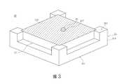
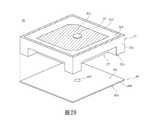
請參閱圖2及圖3,分別為本發明多頻天線裝置一實施例之頂部及底部立體示意圖。如圖所示,多頻天線裝置20主要包括一絕緣基體21、至少一第一電極層231、至少一第二電極層233、至少一第三電極層235、至少一導電元件25及至少一凹槽27。Please refer to FIG. 2 and FIG. 3, which are the top and bottom perspective diagrams of an embodiment of the multi-band antenna device of the present invention, respectively. As shown in the figure, the
絕緣基體21包括一第一表面211、一第二表面213、至少一側表面215及至少一第一通孔217,其中第一表面211與第二表面213為隔著絕緣基體21相對的兩個表面,例如第一表面211為頂表面,而第二表面213為底表面。此外第一表面211經由側表面215連接第二表面213,例如絕緣基體21可為一多邊型柱體或一圓柱體。第一通孔217穿透絕緣基體21,例如第一通孔217連通絕緣基體21的第一表面211及第二表面213。The
第一電極層231及第二電極層233設置於絕緣基體21的第一表面211,其中第二電極層233位於第一電極層231的外圍,且第一電極層231及第二電極層233不相接觸。The
在本發明一實施例中,如圖2所示,第二電極層233可緊靠著絕緣基體21的各個側表面215設置,如圖4所示。在不同實施例中,如圖2及圖6所示,第二電極層233亦可不靠著絕緣基體21的各個側表面215,並與各個側表面215之間存在一間隙212。In an embodiment of the present invention, as shown in FIG. 2, the
在本發明一實施例中,第二電極層233的數量為一個,其中第二電極層233可為連續的環狀構造,並環繞設置在第一電極層231的周圍,如圖4所示。例如第二電極層233為環狀構造,並可在絕緣基體21的第一表面211上形成一設置區域219,此設置區域219為第二電極層233所環繞出來的內部區域,而第一電極層231則設置在設置區域219內。在本發明另一實施例中,第二電極層233的數量可為複數個,且複數個第二電極層233設置在第一電極層231的外圍,如圖5所示。In an embodiment of the present invention, the number of the
在本發明一實施例中,如圖4所示,第一電極層231可不設置在設置區域219的中央或中心,也就是說偏向設置區域219的某一側邊或某一角落。例如第一電極層231可為多邊形,並可能包括四個以上的邊,其中第一電極層231的四個相對比較大的邊與第二電極層233的四個相鄰的邊之間具有四個相對應的間距。最小的間距為第一間距L1,而依順時針方向分別為第二間距L2、第三間距L3及第四間距L4,其中第一間距L1不等於第三間距L3,而第二間距L2不等於第四間距L4。In an embodiment of the present invention, as shown in FIG. 4, the
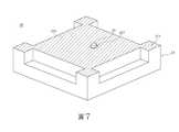
第三電極層235設置在絕緣基體21第二表面213的部份區域,如圖3所示,或者是將第三電極層235設置在絕緣基體21全部的第二表面213,如圖7所示,其中第三電極層235隔著絕緣基體與第一電極層231及/或第二電極層233相對。導電元件25穿過絕緣基體21上的第一通孔217,並電性連接第一電極層231,且不接觸第三電極層235。The
具體來說,第一電極層231及/或第三電極層235亦設置穿孔,其中設置在絕緣基體21上的第一電極層231及第三電極層235的穿孔與絕緣基體21上的第一通孔217的位置,構成部分或全部重疊。導電元件25的截面積小於絕緣基體21的第一通孔217的截面積,使得導電元件25可放入基體21的第一通孔217內。在本發明一實施例中,導電元件25的一端可連接第一電極層231,而導電元件25的另一端則用以電性連接一訊號饋入端(未顯示)。Specifically, the
第一電極層231用以產生一第一共振頻率,而第二電極層233則用以產生一第二共振頻率,且第一共振頻率高於第二共振頻率。The
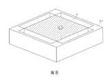
凹槽27設置於絕緣基體21的側表面215及/或第二表面213,其中凹槽27在第一表面的投影與第二電極層233完全或部分重疊。在本發明一實施例中,如圖3所示,凹槽27是設置在絕緣基體21的各個側表面215。在不同實施例中,如圖8所示,凹槽27則是設置在絕緣基體21的第二表面213。此外圖3及圖8的凹槽27並未貫穿絕緣基體21,在不同實施例中,凹槽27亦可貫穿絕緣基體21。The
本發明其中一個特點在於,在絕緣基體21的第二表面213及/或至少一側表面215上設置凹槽27,並使得凹槽27在第一表面的投影與設置在絕緣基體21的第一表面211上的第二電極層233完全或部分重疊。藉由凹槽27的設置,將可改變介於第二電極層233與第三電極層235之間的夾層的有效介電係數,也可以改變介於第二電極層233與多頻天線裝置20下方接地平面29之間的有效介電係數,如圖9所示,其中多頻天線裝置20設置在接地平面29(例如:電路板上的接地平面)上,並改變第二電極層233所產生的第二共振頻率的頻率值,例如:透過凹槽27的設置將可降低介於第二電極層233與第三電極層235及/或接地平面29之間的夾層的有效介電係數,並提高第二電極層233所產生的第二共振頻率。One of the features of the present invention is that a
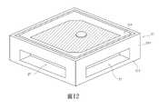
在不同實施例中,亦可改變絕緣基體21上設置的凹槽27的位置,例如於絕緣基體21的各個側表面215上分別設置一個或多個凹槽27,如圖3所示。此外亦可僅在絕緣基體21的部分側表面215上設置一個或多個凹槽27,其中各個凹槽27以對稱的方式設置,例如凹槽27分別設置在絕緣基體21相對的側表面215,如圖10所示。當然亦可將凹槽27環繞設置在絕緣基體21的側表面215,如圖11所示。此外亦可將凹槽27設置在絕緣基體21的部分或全部的側表面215,且凹槽27沒有延伸到絕緣基體21的第一表面211及第二表面213,如圖12所示。In different embodiments, the positions of the
在實際應用時可改變凹槽27在第一表面的投影與第二電極層233的重疊面積、改變凹槽27沿著側表面215上的縱向深度及/或改變凹槽27的設置位置,以調整第二電極層233所產生的第二共振頻率,並使得第二共振頻率符合多頻天線裝置20的設計需求。In practical applications, the overlap area of the projection of the
在本發明另一實施例中,絕緣基體21上的第一通孔217的數量亦可為兩個,如圖13及14所示,其中兩個第一通孔217皆穿透絕緣基體21,並分別將兩個導電元件25設置在兩個第一通孔217內,兩個導電元件25分別連接第一電極層211,且不接觸第三電極層235,並分別連接訊號饋入端(未顯示)。In another embodiment of the present invention, the number of the first through
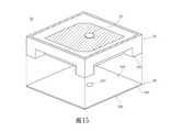
請參閱圖15及圖16,分別為本發明多頻天線裝置一實施例之頂部及底部的立體分解圖。本發明實施例的多頻天線裝置30與上述實施例的多頻天線裝置20相似,主要的差別在於多頻天線裝置30還包括一承載基體39。承載基體39可由絕緣材料所製作,亦可由金屬或導電材質所製作,並包括一第三表面391、一第四表面393及至少一側表面395。第三表面391與第四表面393為隔著承載基體39相對的兩個表面,且第三表面391經由側表面395連接第四表面393。Please refer to FIG. 15 and FIG. 16, which are respectively an exploded perspective view of the top and bottom of an embodiment of the multi-band antenna device of the present invention. The
承載基體39包括至少一第二通孔397,其中第二通孔397穿透承載基體39。承載基體39透過第三表面391之全部或部分區域附著於絕緣基體21的第二表面213,其中承載基體39的第二通孔397與絕緣基體21的第一通孔217相連通,而導電元件25則穿過第一通孔217及第二通孔397。The supporting
在本發明一實施例中,亦可於承載基體39的第四表面393上設置一第四電極層237,當然第四電極層237並非本發明的必要構件,亦非本發明權利範圍的限制。In an embodiment of the present invention, a
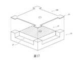
在本發明另一實施例中,如圖17所示,承載基體39亦可包括至少一鏤空區399,其中承載基板39的鏤空區399可和絕緣基體21上凹槽27,部分區域重疊或全部重疊,甚至完全不重疊。此外鏤空區399的截面積可大於、等於或小於凹槽27的截面積。In another embodiment of the present invention, as shown in FIG. 17, the
在本發明另一實施例中,多頻天線裝置30上亦可不用設置第三電極層235及第四電極層237,具體來說多頻天線裝置30僅透過第一電極層231及第二電極層233,亦可產生兩種以上的共振頻率。In another embodiment of the present invention, the
請參閱圖18及圖19,分別為本發明多頻天線裝置又一實施例之頂部及底部分解立體示意圖。如圖所示,多頻天線裝置40主要包括一絕緣基體41、至少一第一電極層431、至少一第二電極層433、至少一第三電極層435、一承載基體47、至少一導電元件45及至少一凹槽49。Please refer to FIG. 18 and FIG. 19, which are respectively an exploded perspective view of the top and bottom of another embodiment of the multi-band antenna device of the present invention. As shown in the figure, the
絕緣基體41包括一第一表面411、一第二表面413、至少一側表面415及至少一第一通孔417,其中第一表面411與第二表面413為隔著絕緣基體41相對的兩個表面,例如第一表面411為頂表面,而第二表面413為底表面。此外第一表面411經由側表面415連接第二表面413,使得絕緣基體41為一多邊型柱體或一圓柱體。第一通孔417穿透絕緣基體41,例如第一通孔417連通絕緣基體41的第一表面411及第二表面413。The insulating
第一電極層431及第二電極層433設置於絕緣基體41的第一表面411,其中第二電極層433位於第一電極層431的外圍,且第一電極層431及第二電極層433不相接觸。The
第三電極層435設置在絕緣基體41的第二表面413,並與第一電極層431及/或第二電極層433相對。導電元件45穿過絕緣基體41上的第一通孔417,並電性連接第一電極層431,且不接觸第三電極層435。The
承載基體47包括一第三表面471、一第四表面473及至少一側表面475,其中第三表面471與第四表面473為隔著承載基體47相對的兩個表面。第三表面471經由側表面475連接第四表面473,而第二通孔477則穿透承載基體47。承載基體47的第三表面471之全部或部分區域附著於絕緣基體41的第二表面413,其中承載基體47的第二通孔477與絕緣基體41的第一通孔417相連通。The supporting
導電元件45穿過第一通孔417及第二通孔477,並電性連接第一電極層431,且不接觸第三電極層435。凹槽49設置於承載基體47的側表面475及/或第三表面471及/或第四表面473,其中凹槽49在第一表面的投影與第二電極層433完全或部分重疊。第一電極層431用以產生一第一共振頻率,而第二電極層433則用以產生一第二共振頻率,且第一共振頻率高於第二共振頻率。凹槽49的數量可為複數個,並以對稱的方式設置在承載基體47的側表面475及/或第三表面471及/或第四表面473。The
在本發明一實施例中承載基體47可為絕緣材質,並可於承載基體47的第四表面473上設置至少一第四電極層437,並使得第四電極層437不接觸導電元件45。此外第四電極層437的面積大於第三電極層435的面積。在本發明另一實施例中,承載基體47亦可由金屬材質所製成,並使得承載基體47不接觸導電元件45。具體來說當承載基體47為金屬材質時,便不需要額外設置第四電極層437。In an embodiment of the present invention, the supporting
在本發明一實施例中,第一電極層431未接觸第二電極層433,並在第一電極層431及第二電極層433之間形成距離不等的間距,俯視圖如圖4所示。此外第一通孔417及第二通孔477的數量亦分別可為兩個,兩個第一通孔417及兩個第二通孔477分別對應連通,並分別將兩個導電元件45分別設置在兩個第一通孔417及兩個第二通孔477內,且兩個導電元件45的一端分別連接第一電極層431,不接觸第三電極層435,而導電元件45的另一端則分別連接訊號饋入端(未顯示)。In an embodiment of the present invention, the
在本發明另一實施例中,多頻天線裝置40上亦可不用設置第三電極層435及/或第四電極層437,具體來說多頻天線裝置40僅透過第一電極層431及第二電極層433,便可產生兩種以上的共振頻率。此外可將至少一凹槽49設置於絕緣基體41的側表面或第二表面213,或者是設置於承載基體49的側表面或第三表面471或第四表面473,以達到調整多頻天線裝置40產生的共振頻率的目的。In another embodiment of the present invention, the
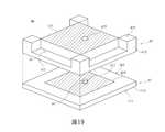
請參閱圖20及圖21,分別為本發明多頻天線裝置又一實施例之頂部及底部立體示意圖。如圖所示,多頻天線裝置50主要包括一絕緣基體21、至少一第一電極層531、至少一第二電極層533、至少一導電元件25、至少一凹槽27及一承載基體59。Please refer to FIG. 20 and FIG. 21, which are respectively a top and bottom perspective schematic diagrams of another embodiment of a multi-band antenna device of the present invention. As shown in the figure, the
絕緣基體21包括一第一表面211、一第二表面213、至少一側表面215及至少一第一通孔217,其中第一表面211與第二表面213為隔著絕緣基體21相對的兩個表面,例如第一表面211為頂表面,而第二表面213為底表面。此外第一表面211經由側表面215連接第二表面213,使得絕緣基體21為一多邊型柱體或一圓柱體。第一通孔217穿透絕緣基體21,例如第一通孔217連通絕緣基體21的第一表面211及第二表面213。The insulating
第一電極層531及第二電極層533設置於絕緣基體21的第一表面211,其中第二電極層533位於第一電極層531的外圍,且第一電極層531及第二電極層533不相接觸。The
凹槽27設置於絕緣基體21的側表面215及/或第二表面213,其中凹槽27在第一表面的投影與第二電極層533完全或部分重疊。第一電極層531用以產生一第一共振頻率,而第二電極層533則用以產生一第二共振頻率,且第一共振頻率高於第二共振頻率。The
承載基體59包括一第三表面591、一第四表面593及至少一側表面595,其中第三表面591與第四表面593為隔著承載基體59相對的兩個表面,且第三表面591經由側表面595連接第四表面593,而第二通孔597穿透承載基體59。The supporting
承載基體59的第三表面591之全部或部分區域附著於絕緣基體21的第二表面213,其中承載基體59的第二通孔597與絕緣基體21的第一通孔217相連通。導電元件25穿過第一通孔217及第二通孔597並電性連接第一電極層531。具體來說,本發明實施例與圖15及圖16的差異處在於,本發明實施例的絕緣基體21的第二表面213上並未設置導電層。All or part of the
在本發明一實施例中,承載基體59可為絕緣材質,並可於承載基體59的第四表面593上設置至少一第三電極層535,並使得第三電極層535不接觸導電元件25。在本發明另一實施例中,承載基體59亦可由金屬材質所製成,並使得承載基體59不接觸導電元件25。具體來說當承載基體59為金屬材質時,便不需要額外設置第三電極層535。In an embodiment of the present invention, the
在本發明另一實施例中,除了於絕緣基體21上設置凹槽27外,亦可於承載基體39、47、59上設置凹槽49,其中承載基體39、47、59的凹槽49可面向絕緣基體21的凹槽27,例如凹槽49設置於承載基體39、47、59的上表面,使得承載基體39、47、59的凹槽49與絕緣基體21的凹槽27連通,如圖22所示。當然凹槽49亦可設置在承載基體39、47、59的下表面,使得承載基體39、47、59的凹槽49與絕緣基體21的凹槽27朝同一個方向,如圖23所示。當然,凹槽49也可以只設置在承載基體39、47、59的側表面。In another embodiment of the present invention, in addition to providing
以上所述者,僅為本發明之較佳實施例而已,並非用來限定本發明實施之範圍,即凡依本發明申請專利範圍所述之形狀、構造、特徵及精神所為之均等變化與修飾,均應包括於本發明之申請專利範圍內。The above are only the preferred embodiments of the present invention, and are not used to limit the scope of implementation of the present invention, that is, all the shapes, structures, characteristics and spirits described in the scope of the patent application of the present invention are equally changed and modified. , Should be included in the scope of patent application of the present invention.
10‧‧‧微帶天線11‧‧‧絕緣基體13‧‧‧第一導電層15‧‧‧第二導電層171‧‧‧導電元件20‧‧‧多頻天線裝置21‧‧‧絕緣基體211‧‧‧第一表面212‧‧‧間隙213‧‧‧第二表面215‧‧‧側表面217‧‧‧第一通孔219‧‧‧設置區域231‧‧‧第一電極層233‧‧‧第二電極層235‧‧‧第三電極層237‧‧‧第四電極層25‧‧‧導電元件27‧‧‧凹槽29‧‧‧接地平面30‧‧‧多頻天線裝置39‧‧‧承載基體391‧‧‧第三表面393‧‧‧第四表面395‧‧‧側表面397‧‧‧第二通孔399‧‧‧鏤空區40‧‧‧多頻天線裝置41‧‧‧絕緣基體411‧‧‧第一表面413‧‧‧第二表面415‧‧‧側表面417‧‧‧第一通孔431‧‧‧第一電極層433‧‧‧第二電極層435‧‧‧第三電極層437‧‧‧第四電極層45‧‧‧導電元件47‧‧‧承載基體471‧‧‧第三表面473‧‧‧第四表面475‧‧‧側表面477‧‧‧第二通孔49‧‧‧凹槽50‧‧‧多頻天線裝置531‧‧‧第一電極層533‧‧‧第二電極層535‧‧‧第三電極層59‧‧‧承載基體591‧‧‧第三表面593‧‧‧第四表面595‧‧‧側表面597‧‧‧第二通孔10‧‧‧Microstrip antenna 11‧‧‧Insulating substrate 13‧‧‧First conductive layer 15‧‧‧Second conductive layer 171‧‧‧Conductive element 20‧‧‧Multi-frequency antenna device 21‧‧‧Insulating substrate 211 ‧‧‧First surface 212‧‧‧Gap 213‧‧‧Second surface 215‧‧‧Side surface 217‧‧‧First through hole 219‧‧‧Setting area 231‧‧‧First electrode layer 233‧‧‧ Second electrode layer 235‧‧‧ Third electrode layer 237‧‧‧ Fourth electrode layer 25‧‧‧Conductive element 27‧‧‧ Groove 29‧‧‧Ground plane 30‧‧‧Multi-frequency antenna device 39‧‧‧ Carrying base 391‧‧‧Third surface 393‧‧‧Fourth surface 395‧‧‧Side surface 397‧‧‧Second through hole 399‧‧‧ Hollow area 40‧‧‧Multi-frequency antenna device 41‧‧‧Insulating substrate 411‧‧‧First surface 413‧‧‧Second surface 415‧‧‧Side surface 417‧‧‧First through hole 431‧‧‧First electrode layer 433‧‧‧Second electrode layer 435‧‧‧Third Electrode layer 437‧‧‧Fourth electrode layer 45‧‧‧Conductive element 47‧‧‧Carrier base 471‧‧‧Third surface 473‧‧‧Fourth surface 475‧‧‧Side surface 477‧‧‧Second through hole 49‧‧‧ Groove 50‧‧‧Multi-frequency antenna device 531‧‧‧First electrode layer 533‧‧‧Second electrode layer 535‧‧‧Third electrode layer 59‧‧‧Carrier base 591‧‧‧Third Surface 593‧‧‧Fourth surface 595‧‧‧Side surface 597‧‧‧Second through hole
圖1:為習用微帶天線之立體透視圖。Figure 1: A perspective view of a conventional microstrip antenna.
圖2:為本發明多頻天線裝置一實施例之頂部的立體示意圖。Fig. 2 is a three-dimensional schematic diagram of the top of an embodiment of the multi-band antenna device of the present invention.
圖3:為本發明多頻天線裝置一實施例之底部的立體示意圖。Fig. 3 is a three-dimensional schematic diagram of the bottom of an embodiment of the multi-band antenna device of the present invention.
圖4:為本發明多頻天線裝置一實施例之俯視圖。Fig. 4 is a top view of an embodiment of the multi-band antenna device of the present invention.
圖5:為本發明多頻天線裝置又一實施例的俯視圖。Fig. 5 is a top view of another embodiment of the multi-frequency antenna device of the present invention.
圖6:為本發明多頻天線裝置又一實施例之頂部的立體示意圖。Fig. 6 is a three-dimensional schematic diagram of the top of another embodiment of the multi-band antenna device of the present invention.
圖7:為本發明多頻天線裝置又一實施例之底部的立體示意圖。Fig. 7 is a three-dimensional schematic diagram of the bottom of another embodiment of the multi-band antenna device of the present invention.
圖8:為本發明多頻天線裝置又一實施例之底部的立體示意圖。Fig. 8 is a three-dimensional schematic diagram of the bottom of another embodiment of the multi-band antenna device of the present invention.
圖9:為本發明多頻天線裝置又一實施例之頂部的立體示意圖。Fig. 9 is a three-dimensional schematic diagram of the top of another embodiment of the multi-band antenna device of the present invention.
圖10:為本發明多頻天線裝置又一實施例之底部的立體示意圖。Fig. 10 is a three-dimensional schematic diagram of the bottom of another embodiment of the multi-band antenna device of the present invention.
圖11:為本發明多頻天線裝置又一實施例之底部的立體示意圖。Fig. 11 is a three-dimensional schematic diagram of the bottom of another embodiment of the multi-band antenna device of the present invention.
圖12:為本發明多頻天線裝置又一實施例之頂部的立體示意圖。Fig. 12 is a three-dimensional schematic diagram of the top of another embodiment of the multi-band antenna device of the present invention.
圖13:為本發明多頻天線裝置又一實施例之頂部的立體示意圖。Fig. 13 is a three-dimensional schematic diagram of the top of another embodiment of the multi-band antenna device of the present invention.
圖14:為本發明多頻天線裝置又一實施例之底部的立體示意圖。Fig. 14 is a three-dimensional schematic diagram of the bottom of another embodiment of the multi-band antenna device of the present invention.
圖15:為本發明多頻天線裝置又一實施例之頂部的立體分解圖。Fig. 15 is a perspective exploded view of the top of another embodiment of the multi-band antenna device of the present invention.
圖16:為本發明多頻天線裝置又一實施例之底部的立體分解圖。Fig. 16 is a perspective exploded view of the bottom of another embodiment of the multi-band antenna device of the present invention.
圖17:為本發明多頻天線裝置又一實施例之底部的立體分解圖。Fig. 17 is a perspective exploded view of the bottom of another embodiment of the multi-band antenna device of the present invention.
圖18:為本發明多頻天線裝置又一實施例之頂部的立體分解圖。Fig. 18 is a perspective exploded view of the top of another embodiment of the multi-band antenna device of the present invention.
圖19:為本發明多頻天線裝置又一實施例之底部的立體分解圖。Fig. 19 is a perspective exploded view of the bottom of another embodiment of the multi-band antenna device of the present invention.
圖20:為本發明多頻天線裝置又一實施例之頂部的立體分解圖。Fig. 20 is a perspective exploded view of the top of another embodiment of the multi-band antenna device of the present invention.
圖21:為本發明多頻天線裝置又一實施例之底部的立體分解圖。Fig. 21 is a perspective exploded view of the bottom of another embodiment of the multi-band antenna device of the present invention.
圖22:為本發明多頻天線裝置又一實施例之頂部的立體示意圖。Fig. 22 is a three-dimensional schematic diagram of the top of another embodiment of the multi-band antenna device of the present invention.
圖23:為本發明多頻天線裝置又一實施例之頂部的立體示意圖。Fig. 23 is a three-dimensional schematic diagram of the top of another embodiment of the multi-band antenna device of the present invention.
20‧‧‧多頻天線裝置20‧‧‧Multi-frequency antenna device
21‧‧‧絕緣基體21‧‧‧Insulating substrate
211‧‧‧第一表面211‧‧‧First surface
212‧‧‧間隙212‧‧‧Gap
213‧‧‧第二表面213‧‧‧Second Surface
215‧‧‧側表面215‧‧‧Side surface
231‧‧‧第一電極層231‧‧‧First electrode layer
233‧‧‧第二電極層233‧‧‧Second electrode layer
25‧‧‧導電元件25‧‧‧Conductive element
27‧‧‧凹槽27‧‧‧Groove
Claims (20)
Translated fromChineseApplications Claiming Priority (3)
| Application Number | Priority Date | Filing Date | Title |
|---|---|---|---|
| CN107205495 | 2018-04-27 | ||
| TW107205495 | 2018-04-27 | ||
| TW107205495 | 2018-04-27 |
Publications (2)
| Publication Number | Publication Date |
|---|---|
| TW201946332A TW201946332A (en) | 2019-12-01 |
| TWI733042Btrue TWI733042B (en) | 2021-07-11 |
Family
ID=65035182
Family Applications (2)
| Application Number | Title | Priority Date | Filing Date |
|---|---|---|---|
| TW107210500UTWM569942U (en) | 2018-04-27 | 2018-08-01 | Multi-band antenna apparatus |
| TW107126705ATWI733042B (en) | 2018-04-27 | 2018-08-01 | Multi-frequency antenna device |
Family Applications Before (1)
| Application Number | Title | Priority Date | Filing Date |
|---|---|---|---|
| TW107210500UTWM569942U (en) | 2018-04-27 | 2018-08-01 | Multi-band antenna apparatus |
Country Status (4)
| Country | Link |
|---|---|
| US (1) | US10847884B2 (en) |
| JP (1) | JP3221949U (en) |
| DE (1) | DE202019102334U1 (en) |
| TW (2) | TWM569942U (en) |
Families Citing this family (3)
| Publication number | Priority date | Publication date | Assignee | Title |
|---|---|---|---|---|
| TWI715438B (en)* | 2020-02-12 | 2021-01-01 | 和碩聯合科技股份有限公司 | Antenna structure |
| TWI822024B (en)* | 2022-05-03 | 2023-11-11 | 台灣禾邦電子有限公司 | Dual band antenna module |
| TWI872792B (en)* | 2023-11-07 | 2025-02-11 | 翰緯科技股份有限公司 | Thin embedded antenna structure |
Citations (3)
| Publication number | Priority date | Publication date | Assignee | Title |
|---|---|---|---|---|
| TW456067B (en)* | 1999-05-25 | 2001-09-21 | Murata Manufacturing Co | Dielectric resonator, filter, duplexer, oscillator and communication apparatus |
| US20090058731A1 (en)* | 2007-08-30 | 2009-03-05 | Gm Global Technology Operations, Inc. | Dual Band Stacked Patch Antenna |
| US20120050126A1 (en)* | 2010-08-31 | 2012-03-01 | Ace Technologies Corp. | Patch antenna synchronously generating linearly polarized wave and circularly polarized wave and generating method thereof |
Family Cites Families (8)
| Publication number | Priority date | Publication date | Assignee | Title |
|---|---|---|---|---|
| JP2004007559A (en)* | 2002-04-25 | 2004-01-08 | Matsushita Electric Ind Co Ltd | Multi-resonance antenna, antenna module, and wireless device using multi-resonance antenna |
| US6836247B2 (en)* | 2002-09-19 | 2004-12-28 | Topcon Gps Llc | Antenna structures for reducing the effects of multipath radio signals |
| US7164385B2 (en)* | 2005-06-06 | 2007-01-16 | Receptec Holdings, Llc | Single-feed multi-frequency multi-polarization antenna |
| CN101919114B (en)* | 2007-10-11 | 2013-09-04 | 泰科电子服务有限责任公司 | Single-layer metallization and via-free metamaterial structure |
| JP4818443B2 (en)* | 2009-12-24 | 2011-11-16 | 株式会社東芝 | Coupler device |
| US8830128B2 (en)* | 2011-06-14 | 2014-09-09 | Kathrein Automotive North America, Inc. | Single feed multi-frequency multi-polarization antenna |
| TWI473346B (en)* | 2011-07-28 | 2015-02-11 | Wistron Neweb Corp | Dualband circularly polarization antenna |
| TWM455997U (en)* | 2013-01-21 | 2013-06-21 | Unictron Technologies Corp | Coupling feeding type of micro-strip antenna |
- 2018
- 2018-08-01TWTW107210500Upatent/TWM569942U/enunknown
- 2018-08-01TWTW107126705Apatent/TWI733042B/enactive
- 2019
- 2019-04-18USUS16/388,792patent/US10847884B2/enactiveActive
- 2019-04-18JPJP2019001412Upatent/JP3221949U/enactiveActive
- 2019-04-25DEDE202019102334.1Upatent/DE202019102334U1/enactiveActive
Patent Citations (3)
| Publication number | Priority date | Publication date | Assignee | Title |
|---|---|---|---|---|
| TW456067B (en)* | 1999-05-25 | 2001-09-21 | Murata Manufacturing Co | Dielectric resonator, filter, duplexer, oscillator and communication apparatus |
| US20090058731A1 (en)* | 2007-08-30 | 2009-03-05 | Gm Global Technology Operations, Inc. | Dual Band Stacked Patch Antenna |
| US20120050126A1 (en)* | 2010-08-31 | 2012-03-01 | Ace Technologies Corp. | Patch antenna synchronously generating linearly polarized wave and circularly polarized wave and generating method thereof |
Also Published As
| Publication number | Publication date |
|---|---|
| JP3221949U (en) | 2019-06-27 |
| TWM569942U (en) | 2018-11-11 |
| DE202019102334U1 (en) | 2019-05-03 |
| TW201946332A (en) | 2019-12-01 |
| US10847884B2 (en) | 2020-11-24 |
| US20190334239A1 (en) | 2019-10-31 |
Similar Documents
| Publication | Publication Date | Title |
|---|---|---|
| KR101067118B1 (en) | Dielectric resonator antenna embedded in multilayer board | |
| JP7047084B2 (en) | Patch antenna corresponding to the cavity | |
| US9548544B2 (en) | Antenna element for signals with three polarizations | |
| US9865928B2 (en) | Dual-polarized antenna | |
| US20150303576A1 (en) | Miniaturized Patch Antenna | |
| TWI733042B (en) | Multi-frequency antenna device | |
| JPWO2018225537A1 (en) | antenna | |
| US20180083354A1 (en) | Antenna radiating elements and sparse array antennas and method for producing an antenna radiating element | |
| JP2013519275A (en) | Multilayer microstrip antenna | |
| CN109119757B (en) | Multi-frequency antenna device | |
| JP2010503357A (en) | Patch antenna and manufacturing method thereof | |
| US9496623B2 (en) | Dual band multi-layer dipole antennas for wireless electronic devices | |
| JP2020174285A (en) | Antenna device | |
| WO2019064683A1 (en) | Array antenna device | |
| US12272885B2 (en) | Lightweight patch antenna | |
| JP6807946B2 (en) | Antenna, module board and module | |
| US12160043B2 (en) | Antenna device which is suitable for wireless communications according to a 5G network standard, RF transceiver containing an antenna device, and method for use in wireless communications according to a 5G network standard | |
| TWM455997U (en) | Coupling feeding type of micro-strip antenna | |
| KR100870996B1 (en) | Built-in antenna | |
| TW201238147A (en) | Annular slot ring antenna | |
| KR100970016B1 (en) | Built-in Antenna with Stacked Structure | |
| JP6761480B2 (en) | Antenna, module board and module | |
| CN209232953U (en) | Coupling feed-in type microstrip antenna | |
| JP2017063345A (en) | Planar antenna | |
| TWM455264U (en) | Microstrip antenna |