TWI732517B - Electronic package and manufacturing method thereof - Google Patents
Electronic package and manufacturing method thereofDownload PDFInfo
- Publication number
- TWI732517B TWI732517BTW109111986ATW109111986ATWI732517BTW I732517 BTWI732517 BTW I732517BTW 109111986 ATW109111986 ATW 109111986ATW 109111986 ATW109111986 ATW 109111986ATW I732517 BTWI732517 BTW I732517B
- Authority
- TW
- Taiwan
- Prior art keywords
- conductive
- electronic package
- item
- electronic
- patent application
- Prior art date
Links
- 238000004519manufacturing processMethods0.000titleclaimsdescription31
- 238000005538encapsulationMethods0.000claimsdescription38
- 238000005253claddingMethods0.000claimsdescription37
- 239000011248coating agentSubstances0.000claimsdescription34
- 238000000576coating methodMethods0.000claimsdescription34
- 238000004806packaging method and processMethods0.000claimsdescription20
- 238000000034methodMethods0.000claimsdescription11
- 239000000463materialSubstances0.000claimsdescription7
- 238000004100electronic packagingMethods0.000claims1
- 239000008393encapsulating agentSubstances0.000abstract5
- 239000010410layerSubstances0.000description50
- 238000004891communicationMethods0.000description11
- 239000005022packaging materialSubstances0.000description9
- 230000005540biological transmissionEffects0.000description8
- 239000002184metalSubstances0.000description7
- 229910052751metalInorganic materials0.000description7
- 238000013461designMethods0.000description6
- 230000000694effectsEffects0.000description6
- 238000005516engineering processMethods0.000description5
- 239000004642PolyimideSubstances0.000description4
- 229920001721polyimidePolymers0.000description4
- RYGMFSIKBFXOCR-UHFFFAOYSA-NCopperChemical compound[Cu]RYGMFSIKBFXOCR-UHFFFAOYSA-N0.000description3
- 229910052802copperInorganic materials0.000description3
- 239000010949copperSubstances0.000description3
- 230000002093peripheral effectEffects0.000description3
- 239000000758substrateSubstances0.000description3
- 230000008859changeEffects0.000description2
- 150000001875compoundsChemical class0.000description2
- 239000004020conductorSubstances0.000description2
- 239000012792core layerSubstances0.000description2
- 238000011161developmentMethods0.000description2
- 238000010586diagramMethods0.000description2
- 239000003989dielectric materialSubstances0.000description2
- 238000005530etchingMethods0.000description2
- 229920002577polybenzoxazolePolymers0.000description2
- 239000004065semiconductorSubstances0.000description2
- 229910000679solderInorganic materials0.000description2
- 239000004593EpoxySubstances0.000description1
- XUIMIQQOPSSXEZ-UHFFFAOYSA-NSiliconChemical compound[Si]XUIMIQQOPSSXEZ-UHFFFAOYSA-N0.000description1
- 238000005452bendingMethods0.000description1
- 239000003990capacitorSubstances0.000description1
- 238000012993chemical processingMethods0.000description1
- 238000000748compression mouldingMethods0.000description1
- 230000007812deficiencyEffects0.000description1
- 238000007772electroless platingMethods0.000description1
- 238000009713electroplatingMethods0.000description1
- 238000000227grindingMethods0.000description1
- 238000002347injectionMethods0.000description1
- 239000007924injectionSubstances0.000description1
- 239000011810insulating materialSubstances0.000description1
- 238000003475laminationMethods0.000description1
- 239000007788liquidSubstances0.000description1
- 238000003801millingMethods0.000description1
- 238000012986modificationMethods0.000description1
- 230000004048modificationEffects0.000description1
- 238000000465mouldingMethods0.000description1
- 238000012858packaging processMethods0.000description1
- 230000008569processEffects0.000description1
- 238000003672processing methodMethods0.000description1
- 238000012827research and developmentMethods0.000description1
- 229910052710siliconInorganic materials0.000description1
- 239000010703siliconSubstances0.000description1
- 238000004544sputter depositionMethods0.000description1
Images


Classifications
- H—ELECTRICITY
- H01—ELECTRIC ELEMENTS
- H01L—SEMICONDUCTOR DEVICES NOT COVERED BY CLASS H10
- H01L23/00—Details of semiconductor or other solid state devices
- H01L23/28—Encapsulations, e.g. encapsulating layers, coatings, e.g. for protection
- H01L23/31—Encapsulations, e.g. encapsulating layers, coatings, e.g. for protection characterised by the arrangement or shape
- H01L23/3107—Encapsulations, e.g. encapsulating layers, coatings, e.g. for protection characterised by the arrangement or shape the device being completely enclosed
- H—ELECTRICITY
- H01—ELECTRIC ELEMENTS
- H01L—SEMICONDUCTOR DEVICES NOT COVERED BY CLASS H10
- H01L23/00—Details of semiconductor or other solid state devices
- H01L23/48—Arrangements for conducting electric current to or from the solid state body in operation, e.g. leads, terminal arrangements ; Selection of materials therefor
- H01L23/488—Arrangements for conducting electric current to or from the solid state body in operation, e.g. leads, terminal arrangements ; Selection of materials therefor consisting of soldered or bonded constructions
- H01L23/498—Leads, i.e. metallisations or lead-frames on insulating substrates, e.g. chip carriers
- H01L23/49811—Additional leads joined to the metallisation on the insulating substrate, e.g. pins, bumps, wires, flat leads
- H—ELECTRICITY
- H01—ELECTRIC ELEMENTS
- H01L—SEMICONDUCTOR DEVICES NOT COVERED BY CLASS H10
- H01L21/00—Processes or apparatus adapted for the manufacture or treatment of semiconductor or solid state devices or of parts thereof
- H01L21/02—Manufacture or treatment of semiconductor devices or of parts thereof
- H01L21/04—Manufacture or treatment of semiconductor devices or of parts thereof the devices having potential barriers, e.g. a PN junction, depletion layer or carrier concentration layer
- H01L21/50—Assembly of semiconductor devices using processes or apparatus not provided for in a single one of the groups H01L21/18 - H01L21/326 or H10D48/04 - H10D48/07 e.g. sealing of a cap to a base of a container
- H01L21/56—Encapsulations, e.g. encapsulation layers, coatings
- H—ELECTRICITY
- H01—ELECTRIC ELEMENTS
- H01L—SEMICONDUCTOR DEVICES NOT COVERED BY CLASS H10
- H01L23/00—Details of semiconductor or other solid state devices
- H01L23/28—Encapsulations, e.g. encapsulating layers, coatings, e.g. for protection
- H01L23/31—Encapsulations, e.g. encapsulating layers, coatings, e.g. for protection characterised by the arrangement or shape
- H01L23/3107—Encapsulations, e.g. encapsulating layers, coatings, e.g. for protection characterised by the arrangement or shape the device being completely enclosed
- H01L23/3121—Encapsulations, e.g. encapsulating layers, coatings, e.g. for protection characterised by the arrangement or shape the device being completely enclosed a substrate forming part of the encapsulation
- H—ELECTRICITY
- H01—ELECTRIC ELEMENTS
- H01L—SEMICONDUCTOR DEVICES NOT COVERED BY CLASS H10
- H01L23/00—Details of semiconductor or other solid state devices
- H01L23/48—Arrangements for conducting electric current to or from the solid state body in operation, e.g. leads, terminal arrangements ; Selection of materials therefor
- H01L23/488—Arrangements for conducting electric current to or from the solid state body in operation, e.g. leads, terminal arrangements ; Selection of materials therefor consisting of soldered or bonded constructions
- H01L23/498—Leads, i.e. metallisations or lead-frames on insulating substrates, e.g. chip carriers
- H01L23/49861—Lead-frames fixed on or encapsulated in insulating substrates
- H—ELECTRICITY
- H01—ELECTRIC ELEMENTS
- H01L—SEMICONDUCTOR DEVICES NOT COVERED BY CLASS H10
- H01L23/00—Details of semiconductor or other solid state devices
- H01L23/552—Protection against radiation, e.g. light or electromagnetic waves
- H—ELECTRICITY
- H01—ELECTRIC ELEMENTS
- H01L—SEMICONDUCTOR DEVICES NOT COVERED BY CLASS H10
- H01L23/00—Details of semiconductor or other solid state devices
- H01L23/58—Structural electrical arrangements for semiconductor devices not otherwise provided for, e.g. in combination with batteries
- H01L23/64—Impedance arrangements
- H01L23/66—High-frequency adaptations
- H—ELECTRICITY
- H01—ELECTRIC ELEMENTS
- H01L—SEMICONDUCTOR DEVICES NOT COVERED BY CLASS H10
- H01L25/00—Assemblies consisting of a plurality of semiconductor or other solid state devices
- H01L25/16—Assemblies consisting of a plurality of semiconductor or other solid state devices the devices being of types provided for in two or more different subclasses of H10B, H10D, H10F, H10H, H10K or H10N, e.g. forming hybrid circuits
- H—ELECTRICITY
- H01—ELECTRIC ELEMENTS
- H01Q—ANTENNAS, i.e. RADIO AERIALS
- H01Q1/00—Details of, or arrangements associated with, antennas
- H01Q1/12—Supports; Mounting means
- H01Q1/22—Supports; Mounting means by structural association with other equipment or articles
- H01Q1/2283—Supports; Mounting means by structural association with other equipment or articles mounted in or on the surface of a semiconductor substrate as a chip-type antenna or integrated with other components into an IC package
- H—ELECTRICITY
- H01—ELECTRIC ELEMENTS
- H01L—SEMICONDUCTOR DEVICES NOT COVERED BY CLASS H10
- H01L2223/00—Details relating to semiconductor or other solid state devices covered by the group H01L23/00
- H01L2223/58—Structural electrical arrangements for semiconductor devices not otherwise provided for
- H01L2223/64—Impedance arrangements
- H01L2223/66—High-frequency adaptations
- H01L2223/6661—High-frequency adaptations for passive devices
- H01L2223/6677—High-frequency adaptations for passive devices for antenna, e.g. antenna included within housing of semiconductor device
- H—ELECTRICITY
- H01—ELECTRIC ELEMENTS
- H01L—SEMICONDUCTOR DEVICES NOT COVERED BY CLASS H10
- H01L2224/00—Indexing scheme for arrangements for connecting or disconnecting semiconductor or solid-state bodies and methods related thereto as covered by H01L24/00
- H01L2224/01—Means for bonding being attached to, or being formed on, the surface to be connected, e.g. chip-to-package, die-attach, "first-level" interconnects; Manufacturing methods related thereto
- H01L2224/10—Bump connectors; Manufacturing methods related thereto
- H01L2224/12—Structure, shape, material or disposition of the bump connectors prior to the connecting process
- H01L2224/13—Structure, shape, material or disposition of the bump connectors prior to the connecting process of an individual bump connector
- H01L2224/13001—Core members of the bump connector
- H01L2224/13099—Material
- H01L2224/131—Material with a principal constituent of the material being a metal or a metalloid, e.g. boron [B], silicon [Si], germanium [Ge], arsenic [As], antimony [Sb], tellurium [Te] and polonium [Po], and alloys thereof
- H—ELECTRICITY
- H01—ELECTRIC ELEMENTS
- H01L—SEMICONDUCTOR DEVICES NOT COVERED BY CLASS H10
- H01L2224/00—Indexing scheme for arrangements for connecting or disconnecting semiconductor or solid-state bodies and methods related thereto as covered by H01L24/00
- H01L2224/01—Means for bonding being attached to, or being formed on, the surface to be connected, e.g. chip-to-package, die-attach, "first-level" interconnects; Manufacturing methods related thereto
- H01L2224/10—Bump connectors; Manufacturing methods related thereto
- H01L2224/15—Structure, shape, material or disposition of the bump connectors after the connecting process
- H01L2224/16—Structure, shape, material or disposition of the bump connectors after the connecting process of an individual bump connector
- H01L2224/161—Disposition
- H01L2224/16151—Disposition the bump connector connecting between a semiconductor or solid-state body and an item not being a semiconductor or solid-state body, e.g. chip-to-substrate, chip-to-passive
- H01L2224/16221—Disposition the bump connector connecting between a semiconductor or solid-state body and an item not being a semiconductor or solid-state body, e.g. chip-to-substrate, chip-to-passive the body and the item being stacked
- H01L2224/16225—Disposition the bump connector connecting between a semiconductor or solid-state body and an item not being a semiconductor or solid-state body, e.g. chip-to-substrate, chip-to-passive the body and the item being stacked the item being non-metallic, e.g. insulating substrate with or without metallisation
- H01L2224/16227—Disposition the bump connector connecting between a semiconductor or solid-state body and an item not being a semiconductor or solid-state body, e.g. chip-to-substrate, chip-to-passive the body and the item being stacked the item being non-metallic, e.g. insulating substrate with or without metallisation the bump connector connecting to a bond pad of the item
- H—ELECTRICITY
- H01—ELECTRIC ELEMENTS
- H01L—SEMICONDUCTOR DEVICES NOT COVERED BY CLASS H10
- H01L2224/00—Indexing scheme for arrangements for connecting or disconnecting semiconductor or solid-state bodies and methods related thereto as covered by H01L24/00
- H01L2224/01—Means for bonding being attached to, or being formed on, the surface to be connected, e.g. chip-to-package, die-attach, "first-level" interconnects; Manufacturing methods related thereto
- H01L2224/10—Bump connectors; Manufacturing methods related thereto
- H01L2224/15—Structure, shape, material or disposition of the bump connectors after the connecting process
- H01L2224/16—Structure, shape, material or disposition of the bump connectors after the connecting process of an individual bump connector
- H01L2224/161—Disposition
- H01L2224/16151—Disposition the bump connector connecting between a semiconductor or solid-state body and an item not being a semiconductor or solid-state body, e.g. chip-to-substrate, chip-to-passive
- H01L2224/16221—Disposition the bump connector connecting between a semiconductor or solid-state body and an item not being a semiconductor or solid-state body, e.g. chip-to-substrate, chip-to-passive the body and the item being stacked
- H01L2224/16245—Disposition the bump connector connecting between a semiconductor or solid-state body and an item not being a semiconductor or solid-state body, e.g. chip-to-substrate, chip-to-passive the body and the item being stacked the item being metallic
- H—ELECTRICITY
- H01—ELECTRIC ELEMENTS
- H01L—SEMICONDUCTOR DEVICES NOT COVERED BY CLASS H10
- H01L2224/00—Indexing scheme for arrangements for connecting or disconnecting semiconductor or solid-state bodies and methods related thereto as covered by H01L24/00
- H01L2224/01—Means for bonding being attached to, or being formed on, the surface to be connected, e.g. chip-to-package, die-attach, "first-level" interconnects; Manufacturing methods related thereto
- H01L2224/26—Layer connectors, e.g. plate connectors, solder or adhesive layers; Manufacturing methods related thereto
- H01L2224/31—Structure, shape, material or disposition of the layer connectors after the connecting process
- H01L2224/32—Structure, shape, material or disposition of the layer connectors after the connecting process of an individual layer connector
- H01L2224/321—Disposition
- H01L2224/32151—Disposition the layer connector connecting between a semiconductor or solid-state body and an item not being a semiconductor or solid-state body, e.g. chip-to-substrate, chip-to-passive
- H01L2224/32221—Disposition the layer connector connecting between a semiconductor or solid-state body and an item not being a semiconductor or solid-state body, e.g. chip-to-substrate, chip-to-passive the body and the item being stacked
- H01L2224/32225—Disposition the layer connector connecting between a semiconductor or solid-state body and an item not being a semiconductor or solid-state body, e.g. chip-to-substrate, chip-to-passive the body and the item being stacked the item being non-metallic, e.g. insulating substrate with or without metallisation
- H—ELECTRICITY
- H01—ELECTRIC ELEMENTS
- H01L—SEMICONDUCTOR DEVICES NOT COVERED BY CLASS H10
- H01L2224/00—Indexing scheme for arrangements for connecting or disconnecting semiconductor or solid-state bodies and methods related thereto as covered by H01L24/00
- H01L2224/01—Means for bonding being attached to, or being formed on, the surface to be connected, e.g. chip-to-package, die-attach, "first-level" interconnects; Manufacturing methods related thereto
- H01L2224/42—Wire connectors; Manufacturing methods related thereto
- H01L2224/47—Structure, shape, material or disposition of the wire connectors after the connecting process
- H01L2224/48—Structure, shape, material or disposition of the wire connectors after the connecting process of an individual wire connector
- H01L2224/481—Disposition
- H01L2224/48151—Connecting between a semiconductor or solid-state body and an item not being a semiconductor or solid-state body, e.g. chip-to-substrate, chip-to-passive
- H01L2224/48221—Connecting between a semiconductor or solid-state body and an item not being a semiconductor or solid-state body, e.g. chip-to-substrate, chip-to-passive the body and the item being stacked
- H01L2224/48225—Connecting between a semiconductor or solid-state body and an item not being a semiconductor or solid-state body, e.g. chip-to-substrate, chip-to-passive the body and the item being stacked the item being non-metallic, e.g. insulating substrate with or without metallisation
- H01L2224/48227—Connecting between a semiconductor or solid-state body and an item not being a semiconductor or solid-state body, e.g. chip-to-substrate, chip-to-passive the body and the item being stacked the item being non-metallic, e.g. insulating substrate with or without metallisation connecting the wire to a bond pad of the item
- H—ELECTRICITY
- H01—ELECTRIC ELEMENTS
- H01L—SEMICONDUCTOR DEVICES NOT COVERED BY CLASS H10
- H01L2224/00—Indexing scheme for arrangements for connecting or disconnecting semiconductor or solid-state bodies and methods related thereto as covered by H01L24/00
- H01L2224/01—Means for bonding being attached to, or being formed on, the surface to be connected, e.g. chip-to-package, die-attach, "first-level" interconnects; Manufacturing methods related thereto
- H01L2224/42—Wire connectors; Manufacturing methods related thereto
- H01L2224/47—Structure, shape, material or disposition of the wire connectors after the connecting process
- H01L2224/48—Structure, shape, material or disposition of the wire connectors after the connecting process of an individual wire connector
- H01L2224/481—Disposition
- H01L2224/48151—Connecting between a semiconductor or solid-state body and an item not being a semiconductor or solid-state body, e.g. chip-to-substrate, chip-to-passive
- H01L2224/48221—Connecting between a semiconductor or solid-state body and an item not being a semiconductor or solid-state body, e.g. chip-to-substrate, chip-to-passive the body and the item being stacked
- H01L2224/48245—Connecting between a semiconductor or solid-state body and an item not being a semiconductor or solid-state body, e.g. chip-to-substrate, chip-to-passive the body and the item being stacked the item being metallic
- H01L2224/48247—Connecting between a semiconductor or solid-state body and an item not being a semiconductor or solid-state body, e.g. chip-to-substrate, chip-to-passive the body and the item being stacked the item being metallic connecting the wire to a bond pad of the item
- H—ELECTRICITY
- H01—ELECTRIC ELEMENTS
- H01L—SEMICONDUCTOR DEVICES NOT COVERED BY CLASS H10
- H01L2224/00—Indexing scheme for arrangements for connecting or disconnecting semiconductor or solid-state bodies and methods related thereto as covered by H01L24/00
- H01L2224/73—Means for bonding being of different types provided for in two or more of groups H01L2224/10, H01L2224/18, H01L2224/26, H01L2224/34, H01L2224/42, H01L2224/50, H01L2224/63, H01L2224/71
- H01L2224/732—Location after the connecting process
- H01L2224/73201—Location after the connecting process on the same surface
- H01L2224/73203—Bump and layer connectors
- H01L2224/73204—Bump and layer connectors the bump connector being embedded into the layer connector
- H—ELECTRICITY
- H01—ELECTRIC ELEMENTS
- H01L—SEMICONDUCTOR DEVICES NOT COVERED BY CLASS H10
- H01L2224/00—Indexing scheme for arrangements for connecting or disconnecting semiconductor or solid-state bodies and methods related thereto as covered by H01L24/00
- H01L2224/91—Methods for connecting semiconductor or solid state bodies including different methods provided for in two or more of groups H01L2224/80 - H01L2224/90
- H01L2224/92—Specific sequence of method steps
- H01L2224/921—Connecting a surface with connectors of different types
- H01L2224/9212—Sequential connecting processes
- H01L2224/92122—Sequential connecting processes the first connecting process involving a bump connector
- H01L2224/92125—Sequential connecting processes the first connecting process involving a bump connector the second connecting process involving a layer connector
- H—ELECTRICITY
- H01—ELECTRIC ELEMENTS
- H01L—SEMICONDUCTOR DEVICES NOT COVERED BY CLASS H10
- H01L23/00—Details of semiconductor or other solid state devices
- H01L23/48—Arrangements for conducting electric current to or from the solid state body in operation, e.g. leads, terminal arrangements ; Selection of materials therefor
- H01L23/488—Arrangements for conducting electric current to or from the solid state body in operation, e.g. leads, terminal arrangements ; Selection of materials therefor consisting of soldered or bonded constructions
- H01L23/498—Leads, i.e. metallisations or lead-frames on insulating substrates, e.g. chip carriers
- H01L23/49833—Leads, i.e. metallisations or lead-frames on insulating substrates, e.g. chip carriers the chip support structure consisting of a plurality of insulating substrates
- H—ELECTRICITY
- H01—ELECTRIC ELEMENTS
- H01L—SEMICONDUCTOR DEVICES NOT COVERED BY CLASS H10
- H01L23/00—Details of semiconductor or other solid state devices
- H01L23/48—Arrangements for conducting electric current to or from the solid state body in operation, e.g. leads, terminal arrangements ; Selection of materials therefor
- H01L23/488—Arrangements for conducting electric current to or from the solid state body in operation, e.g. leads, terminal arrangements ; Selection of materials therefor consisting of soldered or bonded constructions
- H01L23/498—Leads, i.e. metallisations or lead-frames on insulating substrates, e.g. chip carriers
- H01L23/49838—Geometry or layout
- H—ELECTRICITY
- H01—ELECTRIC ELEMENTS
- H01L—SEMICONDUCTOR DEVICES NOT COVERED BY CLASS H10
- H01L23/00—Details of semiconductor or other solid state devices
- H01L23/48—Arrangements for conducting electric current to or from the solid state body in operation, e.g. leads, terminal arrangements ; Selection of materials therefor
- H01L23/488—Arrangements for conducting electric current to or from the solid state body in operation, e.g. leads, terminal arrangements ; Selection of materials therefor consisting of soldered or bonded constructions
- H01L23/498—Leads, i.e. metallisations or lead-frames on insulating substrates, e.g. chip carriers
- H01L23/4985—Flexible insulating substrates
- H—ELECTRICITY
- H01—ELECTRIC ELEMENTS
- H01L—SEMICONDUCTOR DEVICES NOT COVERED BY CLASS H10
- H01L24/00—Arrangements for connecting or disconnecting semiconductor or solid-state bodies; Methods or apparatus related thereto
- H01L24/01—Means for bonding being attached to, or being formed on, the surface to be connected, e.g. chip-to-package, die-attach, "first-level" interconnects; Manufacturing methods related thereto
- H01L24/10—Bump connectors ; Manufacturing methods related thereto
- H01L24/12—Structure, shape, material or disposition of the bump connectors prior to the connecting process
- H01L24/13—Structure, shape, material or disposition of the bump connectors prior to the connecting process of an individual bump connector
- H—ELECTRICITY
- H01—ELECTRIC ELEMENTS
- H01L—SEMICONDUCTOR DEVICES NOT COVERED BY CLASS H10
- H01L24/00—Arrangements for connecting or disconnecting semiconductor or solid-state bodies; Methods or apparatus related thereto
- H01L24/01—Means for bonding being attached to, or being formed on, the surface to be connected, e.g. chip-to-package, die-attach, "first-level" interconnects; Manufacturing methods related thereto
- H01L24/10—Bump connectors ; Manufacturing methods related thereto
- H01L24/15—Structure, shape, material or disposition of the bump connectors after the connecting process
- H01L24/16—Structure, shape, material or disposition of the bump connectors after the connecting process of an individual bump connector
- H—ELECTRICITY
- H01—ELECTRIC ELEMENTS
- H01L—SEMICONDUCTOR DEVICES NOT COVERED BY CLASS H10
- H01L2924/00—Indexing scheme for arrangements or methods for connecting or disconnecting semiconductor or solid-state bodies as covered by H01L24/00
- H01L2924/15—Details of package parts other than the semiconductor or other solid state devices to be connected
- H01L2924/151—Die mounting substrate
- H01L2924/153—Connection portion
- H01L2924/1531—Connection portion the connection portion being formed only on the surface of the substrate opposite to the die mounting surface
- H01L2924/15311—Connection portion the connection portion being formed only on the surface of the substrate opposite to the die mounting surface being a ball array, e.g. BGA
- H—ELECTRICITY
- H01—ELECTRIC ELEMENTS
- H01L—SEMICONDUCTOR DEVICES NOT COVERED BY CLASS H10
- H01L2924/00—Indexing scheme for arrangements or methods for connecting or disconnecting semiconductor or solid-state bodies as covered by H01L24/00
- H01L2924/15—Details of package parts other than the semiconductor or other solid state devices to be connected
- H01L2924/181—Encapsulation
- H01L2924/1815—Shape
- H—ELECTRICITY
- H01—ELECTRIC ELEMENTS
- H01L—SEMICONDUCTOR DEVICES NOT COVERED BY CLASS H10
- H01L2924/00—Indexing scheme for arrangements or methods for connecting or disconnecting semiconductor or solid-state bodies as covered by H01L24/00
- H01L2924/19—Details of hybrid assemblies other than the semiconductor or other solid state devices to be connected
- H01L2924/1901—Structure
- H01L2924/1904—Component type
- H01L2924/19041—Component type being a capacitor
- H—ELECTRICITY
- H01—ELECTRIC ELEMENTS
- H01L—SEMICONDUCTOR DEVICES NOT COVERED BY CLASS H10
- H01L2924/00—Indexing scheme for arrangements or methods for connecting or disconnecting semiconductor or solid-state bodies as covered by H01L24/00
- H01L2924/19—Details of hybrid assemblies other than the semiconductor or other solid state devices to be connected
- H01L2924/1901—Structure
- H01L2924/1904—Component type
- H01L2924/19042—Component type being an inductor
- H—ELECTRICITY
- H01—ELECTRIC ELEMENTS
- H01L—SEMICONDUCTOR DEVICES NOT COVERED BY CLASS H10
- H01L2924/00—Indexing scheme for arrangements or methods for connecting or disconnecting semiconductor or solid-state bodies as covered by H01L24/00
- H01L2924/19—Details of hybrid assemblies other than the semiconductor or other solid state devices to be connected
- H01L2924/1901—Structure
- H01L2924/1904—Component type
- H01L2924/19043—Component type being a resistor
- H—ELECTRICITY
- H01—ELECTRIC ELEMENTS
- H01L—SEMICONDUCTOR DEVICES NOT COVERED BY CLASS H10
- H01L2924/00—Indexing scheme for arrangements or methods for connecting or disconnecting semiconductor or solid-state bodies as covered by H01L24/00
- H01L2924/19—Details of hybrid assemblies other than the semiconductor or other solid state devices to be connected
- H01L2924/191—Disposition
- H01L2924/19101—Disposition of discrete passive components
- H01L2924/19105—Disposition of discrete passive components in a side-by-side arrangement on a common die mounting substrate
- H—ELECTRICITY
- H01—ELECTRIC ELEMENTS
- H01L—SEMICONDUCTOR DEVICES NOT COVERED BY CLASS H10
- H01L2924/00—Indexing scheme for arrangements or methods for connecting or disconnecting semiconductor or solid-state bodies as covered by H01L24/00
- H01L2924/30—Technical effects
- H01L2924/301—Electrical effects
- H01L2924/3025—Electromagnetic shielding
Landscapes
- Engineering & Computer Science (AREA)
- Microelectronics & Electronic Packaging (AREA)
- Physics & Mathematics (AREA)
- Power Engineering (AREA)
- Computer Hardware Design (AREA)
- General Physics & Mathematics (AREA)
- Condensed Matter Physics & Semiconductors (AREA)
- Manufacturing & Machinery (AREA)
- Health & Medical Sciences (AREA)
- Electromagnetism (AREA)
- Toxicology (AREA)
- Geometry (AREA)
- Shielding Devices Or Components To Electric Or Magnetic Fields (AREA)
- Structures Or Materials For Encapsulating Or Coating Semiconductor Devices Or Solid State Devices (AREA)
- Structures For Mounting Electric Components On Printed Circuit Boards (AREA)
Abstract
Description
Translated fromChinese本發明係有關一種封裝製程,尤指一種具天線功能之電子封裝件及其製法。The present invention relates to a packaging process, in particular to an electronic package with antenna function and its manufacturing method.
隨著電子產業的蓬勃發展,電子產品也逐漸邁向多功能、高性能的趨勢。目前第四代(4G)的無線傳輸通訊技術已廣泛應用於各式各樣的消費性電子產品以利接收或發送各種無線訊號。With the vigorous development of the electronics industry, electronic products are gradually moving towards the trend of multi-function and high performance. At present, the fourth-generation (4G) wireless transmission communication technology has been widely used in various consumer electronic products to receive or send various wireless signals.
然而,隨著無線通信發展迅速,以及網路資源流量日趨龐大,所需的無線傳輸頻寬也越來越大,故無線傳輸第五代(5G)之研發已呈趨勢。However, with the rapid development of wireless communication and the ever-increasing flow of network resources, the required wireless transmission bandwidth is also increasing. Therefore, the research and development of the fifth generation (5G) of wireless transmission has become a trend.
第1圖係習知無線通訊裝置之立體示意圖。如第1圖所示,該無線通訊裝置1係包括:一配置有電子元件11之電路板10、設於該電路板10上之複數晶片元件16、一天線元件12以及封裝體13。該晶片元件16係設於該電路板10上且電性連接該電路板10。該天線元件12係藉由一傳輸線17電性連接該晶片元件16。該封裝體13覆蓋該晶片元件16與該部分傳輸線17。Figure 1 is a three-dimensional schematic diagram of a conventional wireless communication device. As shown in FIG. 1, the wireless communication device 1 includes: a
惟,習知無線通訊裝置1中,由於5G用天線元件12為了加強訊號強度,該天線元件12需設於靠近該可攜式電子產品之機殼附近處,故該可攜式電子產品可提供設置該天線元件12的空間有限,故需進一步滿足無線通訊裝置1的微小化需求;此外,設於機殼附近處的無線通訊裝置1如何與設於中央的可攜式電子產品之內部其它組件(如主機板)進行電性溝通也是一需解決的問題。However, in the conventional wireless communication device 1, in order to enhance the signal strength of the 5G antenna element 12, the antenna element 12 needs to be located near the casing of the portable electronic product.The sub-products can provide limited space for installing the antenna element 12, so it is necessary to further meet the miniaturization requirements of the wireless communication device 1; in addition, how does the wireless communication device 1 located near the casing compare with the portable electronic product located in the center? The electrical communication of other internal components (such as the motherboard) is also a problem that needs to be solved.
因此,如何克服上述習知技術之種種問題,實已成為目前業界亟待克服之難題。Therefore, how to overcome the various problems of the above-mentioned conventional technology has actually become an urgent problem to be overcome in the industry.
鑑於上述習知技術之種種缺失,本發明提供一種電子封裝件,係包括:承載結構,係具有天線功能;電子元件,係設於該承載結構上且電性連接該承載結構;導電架,係設於該承載結構上且具有複數相分離之導電柱,其中,該複數導電柱係電性連接該承載結構;以及封裝層,係設於該承載結構上以包覆該電子元件及導電架,該封裝層係定義有一體成形之第一包覆部及第二包覆部,該電子元件係位於該第一包覆部中,且該複數導電柱係位於該第二包覆部中,其中,該第一包覆部之高度係高於該第二包覆部之高度,且該複數導電柱之端面係外露於該第二包覆部之表面以供電性連接一連接器。In view of the various deficiencies of the above-mentioned conventional technologies, the present invention provides an electronic package, which includes: a carrying structure, which has an antenna function; an electronic component, which is arranged on the carrying structure and is electrically connected to the carrying structure; and a conductive frame is Is provided on the supporting structure and has a plurality of separated conductive pillars, wherein the plurality of conductive pillars are electrically connected to the supporting structure; and an encapsulation layer is provided on the supporting structure to cover the electronic component and the conductive frame, The encapsulation layer is defined with a first cladding part and a second cladding part that are integrally formed, the electronic component is located in the first cladding part, and the plurality of conductive pillars are located in the second cladding part, wherein The height of the first cladding part is higher than the height of the second cladding part, and the end faces of the plurality of conductive posts are exposed on the surface of the second cladding part to be electrically connected to a connector.
本發明亦提供一種電子封裝件之製法,係包括:提供一具有天線功能之承載結構;將至少一電子元件與至少一導電架設置並電性連接於該承載結構上,且該導電架係具有複數相分離之導電柱;以及形成一封裝層於該承載結構上,以令該封裝層包覆該電子元件及導電架,該封裝層係定義有一體成形之第一包覆部及第二包覆部,該電子元件係位於該第一包覆部中,且該複數導電柱係位於該第二包覆部中,其中,該第一包覆部之高度係高於該第二包覆部之高度,且該複數導電柱之端面係外露於該第二包覆部之表面以供電性連接一連接器。The present invention also provides a method for manufacturing an electronic package, which includes: providing a bearing structure with antenna function; arranging and electrically connecting at least one electronic component and at least one conductive frame to the bearing structure, and the conductive frame has A plurality of separated conductive posts; and forming an encapsulation layer on the carrying structure so that the encapsulation layer covers the electronic component and the conductive frame, and the encapsulation layer is defined with an integrally formed first cladding portion and a second encapsulation Covering part, the electronic component is located in the first covering part, and the plurality of conductive posts areIs located in the second cladding part, wherein the height of the first cladding part is higher than the height of the second cladding part, and the end faces of the plurality of conductive posts are exposed on the surface of the second cladding part to The power supply is connected to a connector.
前述之製法中,該封裝層之製程係於形成包覆該電子元件及導電架之封裝材後,移除部分該封裝材及部分該導電架,以形成該封裝層,使該封裝層具有該第一包覆部與該第二包覆部,且使該複數導電柱之端面係外露於該第二包覆部之表面。In the aforementioned manufacturing method, the process of the packaging layer is to remove part of the packaging material and part of the conductive frame after forming the packaging material covering the electronic component and the conductive frame to form the packaging layer so that the packaging layer has the The first cladding part and the second cladding part, and the end surfaces of the plurality of conductive posts are exposed on the surface of the second cladding part.
前述之電子封裝件及其製法中,該承載結構係包含相堆疊之線路板與天線板。In the aforementioned electronic package and its manufacturing method, the carrying structure includes a circuit board and an antenna board stacked on each other.
前述之電子封裝件及其製法中,復包括以屏蔽結構遮蓋該電子元件。例如,復包括形成該屏蔽結構於該封裝層部分表面,使該屏蔽結構遮蓋該電子元件,且不接觸該複數導電柱。進一步,該導電架復具有至少一埋設於該封裝層中之導電牆,該導電牆與該複數導電柱相分離,且外露於該第二包覆部,並連接該屏蔽結構。或者,該導電架復具有至少一埋設於該封裝層中之導電塊,該導電塊與該導電柱相分離,且外露於該第一包覆部,並連接該屏蔽結構。In the aforementioned electronic package and its manufacturing method, the electronic component is covered with a shielding structure. For example, it includes forming the shielding structure on a part of the surface of the encapsulation layer so that the shielding structure covers the electronic component and does not contact the plurality of conductive pillars. Furthermore, the conductive frame has at least one conductive wall buried in the encapsulation layer, the conductive wall is separated from the plurality of conductive pillars, is exposed to the second coating part, and is connected to the shielding structure. Alternatively, the conductive frame has at least one conductive block buried in the encapsulation layer, the conductive block is separated from the conductive column, and exposed to the first coating part, and is connected to the shielding structure.
前述之電子封裝件及其製法中,復包括設置連接器於該複數導電柱上。In the aforementioned electronic package and its manufacturing method, it further includes arranging a connector on the plurality of conductive posts.
前述之電子封裝件及其製法中,復包括將一配置有連接器之轉接件設於該複數導電柱上。例如,該轉接件係為可撓式電路板。The aforementioned electronic package and its manufacturing method further include placing an adapter with a connector on the plurality of conductive posts. For example, the adapter is a flexible circuit board.
前述之電子封裝件及其製法中,該第二包覆部設置於該承載結構的其中一側。In the aforementioned electronic package and its manufacturing method, the second covering portion is disposed on one side of the carrying structure.
前述之電子封裝件及其製法中,該第二包覆部係設置於該承載結構之角落處。In the aforementioned electronic package and its manufacturing method, the second covering portion is disposed at the corner of the carrying structure.
前述之電子封裝件及其製法中,該封裝層係具有複數該第二包覆部,且該第一包覆部係位於其中兩該第二包覆部之間。In the aforementioned electronic package and its manufacturing method, the packaging layer has a plurality of the second coating portions, and the first coating portion is located between two of the second coating portions.
前述之電子封裝件及其製法中,該封裝層係具有複數該第一包覆部,且該第二包覆部係位於其中兩該第一包覆部之間。In the aforementioned electronic package and its manufacturing method, the packaging layer has a plurality of the first coating portions, and the second coating portion is located between two of the first coating portions.
由上可知,本發明之電子封裝件主要藉由該第一包覆部高於該第二包覆部之設計,使該複數導電柱外露於該第二包覆部,俾供作為接點,因而可依需求將該連接器直接/間接整合於該電子封裝件中,進而使該承載結構之天線可藉由該連接器高自由度地電性連接該電子產品之主機板,使該承載結構可依訊號強度需求設置於靠近該電子產品之機殼附近處,故相較於習知技術,若電子產品採用本發明之電子封裝件,可令其它組件之設計不會受到空間限制,使該電子產品可依需求滿足所有之功能。It can be seen from the above that the electronic package of the present invention mainly uses the design of the first cladding part to be higher than the second cladding part, so that the plurality of conductive posts are exposed to the second cladding part for use as contacts. Therefore, the connector can be directly/indirectly integrated into the electronic package according to requirements, so that the antenna of the carrying structure can be electrically connected to the motherboard of the electronic product through the connector with a high degree of freedom, so that the carrying structure It can be installed near the casing of the electronic product according to the signal strength requirements. Therefore, compared with the conventional technology, if the electronic product adopts the electronic package of the present invention, the design of other components will not be restricted by space. Electronic products can satisfy all functions as required.
1:無線通訊裝置1: wireless communication device
10:電路板10: Circuit board
11:電子元件11: Electronic components
12:天線元件12: Antenna element
13:封裝體13: Package body
16:晶片元件16: chip components
17:傳輸線17: Transmission line
2,2’,2”,3,3’,4:電子封裝件2,2’,2”,3,3’,4: electronic package
20,20’:承載結構20,20’: Bearing structure
20a:第一側20a: first side
20b:第二側20b: second side
20c,230c,231c:側面20c, 230c, 231c: side
200:導電體200: Conductor
201:線路板201: circuit board
202:天線板202: Antenna Board
21,21’,21”:電子元件21,21’,21”: Electronic components
210:導電凸塊210: conductive bump
22,32:導電架22, 32: Conductive frame
220:板體220: Board body
220’:導電塊220’: Conductive block
221,421:導電柱221,421: Conductive post
222:導電牆222: Conductive Wall
23,33,33’:封裝層23,33,33’: Encapsulation layer
23’:封裝材23’: Packaging material
230,330:第一包覆部230, 330: the first cladding part
231,331:第二包覆部231, 331: the second covering part
24,24’:屏蔽結構24,24’: Shielding structure
240:屏蔽部240: shielding part
25:轉接件25: Adapter
26:連接器26: Connector
421c:周面421c: peripheral surface
9:電子產品9: Electronic products
9a:機殼9a: Chassis
90:主機板90: Motherboard
91:支撐架91: support frame
900:連接埠900: Port
A:第一區域A: The first area
B:第二區域B: second area
H1,H2:高度H1, H2: height
第1圖係習知無線通訊裝置之立體示意圖。Figure 1 is a three-dimensional schematic diagram of a conventional wireless communication device.
第2A至2D圖係為本發明之電子封裝件之製法之剖面示意圖。2A to 2D are schematic cross-sectional views of the manufacturing method of the electronic package of the present invention.
第2A’圖係為第2A圖之另一態樣。Figure 2A' is another aspect of Figure 2A.
第2D’圖係為第2D圖之另一態樣。The 2D' picture is another aspect of the 2D picture.
第2D”圖係為第2D’圖之另一態樣。The "2D" picture is another aspect of the 2D' picture.
第2E及2E’圖係為第2D圖之其它態樣。Figures 2E and 2E' are other aspects of Figure 2D.
第2E”圖係為第2E圖之後續應用之剖面示意圖。Figure 2E" is a schematic cross-sectional view of the subsequent application of Figure 2E.
第3A至3C圖係為第2E圖之不同態樣之上視示意圖。Figures 3A to 3C are schematic top views of different aspects of Figure 2E.
第3D及3E圖係為第3A圖之其它態樣之上視示意圖。Figures 3D and 3E are schematic top views of other aspects of Figure 3A.
第3D’及3E’圖係為第3D及3E圖增設屏蔽結構之剖面示意圖。Figures 3D' and 3E' are schematic cross-sectional views of additional shielding structures in Figures 3D and 3E.
第4圖係為本發明之電子封裝件之另一實施例之剖面示意圖。FIG. 4 is a schematic cross-sectional view of another embodiment of the electronic package of the present invention.
第4’圖係為第4圖之上視圖。Figure 4'is a top view of Figure 4.
以下藉由特定的具體實施例說明本發明之實施方式,熟悉此技藝之人士可由本說明書所揭示之內容輕易地瞭解本發明之其他優點及功效。The following specific examples illustrate the implementation of the present invention. Those familiar with the art can easily understand the other advantages and effects of the present invention from the contents disclosed in this specification.
須知,本說明書所附圖式所繪示之結構、比例、大小等,均僅用以配合說明書所揭示之內容,以供熟悉此技藝之人士之瞭解與閱讀,並非用以限定本發明可實施之限定條件,故不具技術上之實質意義,任何結構之修飾、比例關係之改變或大小之調整,在不影響本發明所能產生之功效及所能達成之目的下,均應仍落在本發明所揭示之技術內容得能涵蓋之範圍內。同時,本說明書中所引用之如「上」、「第一」、「第二」及「一」等之用語,亦僅為便於敘述之明瞭,而非用以限定本發明可實施之範圍,其相對關係之改變或調整,在無實質變更技術內容下,當亦視為本發明可實施之範疇。It should be noted that the structure, ratio, size, etc. shown in the drawings in this manual are only used to match the content disclosed in the manual for the understanding and reading of those who are familiar with the art, and are not intended to limit the implementation of the present invention. Therefore, it does not have any technical significance. Any structural modification, proportional relationship change or size adjustment, without affecting the effects and objectives that can be achieved by the present invention, should still fall within the scope of the present invention. The technical content disclosed by the invention can be covered. At the same time, the terms "on", "first", "second" and "one" cited in this specification are only for ease of description and are not used to limit the scope of the present invention. The change or adjustment of the relative relationship shall be regarded as the scope of the implementation of the present invention without substantial changes to the technical content.
第2A至2D圖係為本發明之電子封裝件2之製法之剖面示意圖。2A to 2D are schematic cross-sectional views of the manufacturing method of the
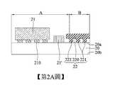
如第2A圖所示,提供一配置有至少一電子元件21,21’與至少一導電架22之承載結構20,且該承載結構20係具有相對之第一側20a與第二側20b,以令該電子元件21,21’與該導電架22均設於該承載結構20之第一側20a。As shown in FIG. 2A, a supporting
於本實施例中,該承載結構20係例如為封裝基板(substrate),其可為具有核心層之線路結構或無核心層(coreless)之線路結構,且其構成係於介電材上形成複數線路層,如扇出(fan out)型重佈線路層(redistribution layer,簡稱RDL)。形成該線路層之材質係例如為銅,且該介電材係例如為聚對二唑苯(Polybenzoxazole,簡稱PBO)、聚醯亞胺(Polyimide,簡稱PI)、預浸材(Prepreg,簡稱PP)等。具體地,該承載結構20之第一側20a上定義有相鄰接之第一區域A與第二區域B,且該第一區域A係作為作用區以配置該電子元件21,21’,而該第二區域B係作為外接區以配置該導電架22。應可理解地,該承載結構20亦可為其它可供承載如晶片等電子元件之承載單元,例如導線架(lead frame)、矽中介板(silicon interposer)或功能模組,並不限於上述。In this embodiment, the carrying
再者,該承載結構20係具有天線功能,如天線基板,其線路層具有天線功能。或者,如第2A’圖所示,該承載結構20’可為天線模組,其由一線路板201與一天線板202相堆疊組合而成,該線路板201係位於該承載結構20’之第一側20a,而該天線板202係位於該承載結構20’之第二側20b,且該線路板201可藉由如銲錫材料之導電體200接置該天線板202。Furthermore, the supporting
又,該電子元件21,21’係為主動元件、被動元件或其二者組合,且該主動元件係例如半導體晶片(如電子元件21),而該被動元件(如電子元件21’)係例如電阻、電容及電感。例如,該半導體晶片係藉由複數如銲錫材料、金屬柱(pillar)或其它等之導電凸塊210以覆晶方式設於該承載結構20之第一側20a之線路層(圖未示)上並電性連接該線路層,且可依需求以如底膠(圖略)包覆該些導電凸塊210;或者,該電子元件21可藉由複數銲線(圖未示)以打線方式電性連接該承載結構20之線路層;亦或,該電子元件21’可直接接觸該承載結構20之線路層。應可理解地,有關電子元件21,21’電性連接承載結構20之方式繁多,並不限於上述。In addition, the
另外,該導電架22係包含一板體220及複數分離設於該板體220上之導電柱221與導電牆222,且該導電架22以其導電柱221與導電牆222立設於該承載結構20之第一側20a之第二區域B上。例如,以蝕刻、雷射或其它方式移除一如銅材之金屬板之部分材質,以形成該導電架22。In addition, the
如第2B圖所示,形成一封裝材23’於該承載結構20之第一側20a上,以包覆該電子元件21,21’與該導電架22。As shown in FIG. 2B, a packaging material 23' is formed on the
於本實施例中,該封裝材23’係為絕緣材,如聚醯亞胺(polyimide,簡稱PI)、乾膜(dry film)、如環氧樹脂(epoxy)之封裝膠體或封裝材(molding compound)。例如,該封裝材23’之製程可選擇液態封膠(liquid compound)、噴塗(injection)、壓合(lamination)或模壓(compression molding)等方式形成於該承載結構20上。In this embodiment, the encapsulating material 23' is an insulating material, such as polyimide (PI), dry film, encapsulating gel such as epoxy, or molding compound). For example, the packaging material 23' can be formed on the supporting
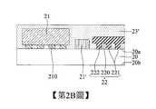
如第2C圖所示,移除部分該封裝材23’及該導電架22之部分板體220,以形成一外觀具缺口之封裝層23,其定義有一位於該第一區域A之第一包覆部230及一位於該第二區域B之第二包覆部231,其中,該第一包覆部230之高度H1係高於該第二包覆部231之高度H2,以令該導電柱221與導電牆222外露於該封裝層23之第二包覆部231,且該導電塊220’(即該板體220之剩餘部分)係外露於該第一包覆部230之側面230c,使該導電柱221作為接點(I/O),且該導電牆222及該導電塊220’作為接地。例如,該導電牆222及該導電塊220’相連接並為一體成型。As shown in Figure 2C, a portion of the packaging material 23' and a portion of the
於本實施例中,使用研磨方式移除該第二區域B上方之部分板體220及部分封裝材23’,以保留該第二區域B上之導電柱221與導電牆222周圍之封裝材23’,俾供作為該第二包覆部231。應可理解地,有關移除方式繁多,如蝕刻、雷射、銑具等,並不限於上述。In this embodiment, a grinding method is used to remove part of the
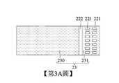
再者,該導電柱221之接點功能可為訊號接點(signal pin)、組裝(SMT)用接點或其他用途等,且其端面形狀可為矩形(如第3A圖所示)、圓形(如第3B圖所示)或其它形狀,並無特別限制。Furthermore, the contact function of the
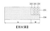
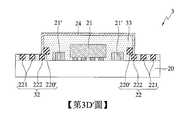
又,該第二包覆部231之範圍可依需求調整,如第3A及3B圖所示之整個第二區域B上方(即該封裝層23之外觀呈階梯狀)或第3C圖所示之部分第二區域B上(其第一包覆部330係延伸至該第二區域B,即該封裝層23之外觀呈缺角狀),以調整該導電柱221作為接點(I/O)之數量。應可理解地,亦可藉由增加該導電架22之數量,以調整該導電柱221作為接點(I/O)之數量,如第3D及3D’圖所示之電子封裝件3,其將兩導電架22,32設於該電子元件21,21’之相對兩側,即令該第一區域A之相對兩側分別定義為第二區域B,使該第一包覆部230位於兩第二包覆部231,331之間,即該封裝層33之外觀呈凸狀。In addition, the range of the
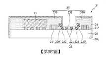
另外,可依電子產品之空間需求,調整該導電架22之位置。例如,該導電架22係遠離該承載件20之第二區域B之側面20c,如第3E及3E’圖所示之電子封裝件3’,其封裝層33’之第一包覆部330係位於該承載件20之相對兩側上以包覆該電子元件21,21’,21”,使該第二包覆部231位於兩第一包覆部230,330之間,即該封裝層33’之外觀呈凹狀。In addition, the position of the
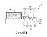
如第2D圖所示,形成一屏蔽結構24於該封裝層23上,以遮蓋該電子元件21,21’,使該電子元件21,21’不會受外界之電磁干擾。As shown in FIG. 2D, a shielding
於本實施例中,該屏蔽結構24之佈設區域可依需求選擇覆蓋該封裝層23之第一包覆部230之全部表面或部分表面(如1/2或1/3),甚至可選擇覆蓋該承載件20之第一區域A之部分側面20c或全部側面20c。例如,該屏蔽結構24可延伸至該第一包覆部230之側面230c以接觸該導電塊220’,甚至接觸該導電牆222。因此,藉由該導電塊220’與該導電牆222外露於該封裝層23,以電性連接該屏蔽結構24,使該屏蔽結構24可透過該導電塊220’與該導電牆222連接該承載件20的接地線路而達到屏蔽的效果。應可理解地,該屏蔽結構24亦可接觸該承載件20之第一區域A之側面20c之線路層,使該屏蔽結構24接地而達到屏蔽的效果。In this embodiment, the layout area of the shielding
再者,可藉由塗佈金屬層(如銅材)之加工方式形成該屏蔽結構24於該封裝層23上,例如,濺鍍(sputtering)、蒸鍍(vaporing)、電鍍、無電電鍍或化鍍等方式;或者,利用蓋設金屬架或金屬罩、或貼膜(foiling)等設置方式形成該屏蔽結構24於該封裝層23上;亦或,可先於該承載結構20上設置如金屬架或金屬罩之屏蔽結構24’,以遮蓋該電子元件21,21’,再以該封裝層23包覆該屏蔽結構24’,如第2D’圖所示之電子封裝件2’。應可理解地,有關屏蔽方式繁多,如第2D”圖所示之電子封裝件2”,其可於該兩電子元件21,21’之間形成至少一電性連接該屏蔽結構24之屏蔽部240(如柱狀或牆狀),故該屏蔽結構之態樣並無特別限制。Furthermore, the shielding
又,該電子封裝件2,2’,3,3’復可依需求於該些導電柱221上接置一連接器26,如第2E圖所示,以藉由該連接器26接合電子產品之主機板之連接埠上,以令該電子封裝件2電性連接該主機板,使該電子封裝件2整合配置於該電子產品中。例如,該連接器26可直接銲接或其它方式設於該導電柱221上以電性連接該導電柱221。In addition, the
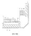
另外,如第2E’圖所示,該電子封裝件2,2’,3,3’亦可依需求將一轉接件25連接該些導電柱221,且將該連接器26設於該轉接件25上。例如,該轉接件25係為軟性或可撓式電路板,其可依需求彎折,並銲接於該導電柱221上以電性連接該導電柱221。具體地,該轉接件25係以其中一端側接置該些導電柱221,而另一端側接置該連接器26,以依電子產品9之內部空間狀況,如第2E”圖所示,藉由彎折該轉接件25(其兩端側之方位約呈90度或其它度數之夾角),令該連接器26接合該電子產品9之主機板90之連接埠900上,使該電子封裝件2電性連接該主機板90,因而能將該電子封裝件2整合配置於該電子產品9中,其中,該電子產品9內可藉由至少一支撐架91固定該電子封裝件2,故當該電子產品9之內部空間有限時,可彎折該轉接件25,以利於該電子產品9之其它組件之設計。In addition, as shown in FIG. 2E', the
因此,本發明之製法中,藉由將封裝材23’研磨形成具缺口之封裝層23,使該導電架22之導電柱221外露於該封裝層23之高度較低之第二包覆部231,俾供作為接點,以電性連接該連接器26或其它用途,因而能將該連接器26直接/間接整合於該電子封裝件2,2’,3,3’中,且該承載結構20,20’之天線(線路層或天線板202)可電性連接該主機板90,使該承載結構20可依訊號強度需求設置於靠近該電子產品9之機殼9a附近處,故相較於習知技術,該電子產品9之內部其它組件(如主機板90)之設計不會受到空間限制,致使該電子產品9可依需求滿足所有之功能。Therefore, in the manufacturing method of the present invention, the packaging material 23' is ground to form a notched
再者,若將該連接器26直接整合於該電子封裝件2,2’,3,3’上,使該主機板90所提供的電能可直接傳輸至該承載結構20,20’,而不需經過其它傳輸路徑(如轉接件25),以避免傳輸電能於通過該轉接件25時產生電性損耗(loss),故不僅可增快傳輸速度,且可提升電性表現(performance)。Furthermore, if the
又,若該電子封裝件2,2’,3,3’與該主機板90距離較遠,則於封裝端需藉由一如軟板型或硬板型之轉接件25連接該連接器26,以增加該電子封裝件2,2’,3,3’設置位置的自由度;此外,封裝端直接焊接該轉接件25可減少該連接器26的使用數量(該承載結構20,20’上無需使用連接器),以降低封裝成本。Moreover, if the
另外,如第4及4’圖所示之導電柱421之周面421c若外露於該第二包覆部231之側面231c(例如,該導電柱421之周面421c齊平該第二包覆部231之側面231c),除了可藉由將該導電柱421接地達到屏蔽的效果之外,亦可藉由該導電柱421與系統端的其他元件(即該電子產品9之內部組件)電性連接以作為訊號聯通及/或接地,故可增加該電子封裝件2,2’,3,3’與系統端之其他元件(即該電子產品9之內部組件)之配置彈性,即該封裝層23之第二包覆部231之側面231c亦可作為外部連接區域。In addition, if the
本發明復提供一種電子封裝件2,2’,2”,3,3’,4,係包括:一承載結構20,20’、至少一電子元件21,21’、一導電架22以及一封裝層23,23’,33,33’。The present invention further provides an
所述之承載結構20,20’係具有天線功能。The supporting
所述之電子元件21,21’係設於該承載結構20,20’上且電性連接該承載結構20,20’。The
所述之導電架22係設於該承載結構20,20’上且具有複數相分離之導電柱221,421,其中,該複數導電柱221,421係電性連接該承載結構20,20’。The
所述之封裝層23,23’,33,33’係設於該承載結構20,20’上以包覆該電子元件21,21’及導電架22,且該封裝層23,23’,33,33’係定義有一體成形之第一包覆部230,330及第二包覆部231,331,該電子元件21,21’係位於該第一包覆部230,330中,且該複數導電柱221,421係位於該第二包覆部231,331中,其中,該第一包覆部230,330之高度H1係高於該第二包覆部231,331之高度H2,且該複數導電柱221,421之端面係外露於該第二包覆部231,331之表面以電性連接一連接器26。The packaging layers 23, 23', 33, 33' are provided on the supporting
於一實施例中,該承載結構20’係包含相堆疊之線路板201與天線板202。In one embodiment, the supporting structure 20' includes a
於一實施例中,所述之電子封裝件2,2’,2”,3,3’,4復包括一遮蓋該電子元件21,21’之屏蔽結構24,24’。例如,該屏蔽結構24係形成於該封裝層23部分表面且遮蓋該電子元件21,該屏蔽結構24不接觸該複數導電柱221,421。進一步,該導電架22復具有至少一埋設於該封裝層23中之導電牆222,該導電牆222與該複數導電柱221,421相分離,且外露於該第二包覆部231,並連接該屏蔽結構24’。或者,該導電架22復具有至少一埋設於該封裝層23中之導電塊220’,該導電塊220’與該導電柱221,421相分離,且外露於該第一包覆部230,並連接該屏蔽結構24’。In one embodiment, the
於一實施例中,該連接器26係接置於該複數導電柱221上。In one embodiment, the
於一實施例中,該連接器26係藉由一接置於該複數導電柱221上之轉接件25電性連接該導電柱221。例如,該轉接件25係為可撓式電路板。In one embodiment, the
於一實施例中,該第二包覆部231係設置於該承載結構20之其中一側。In one embodiment, the
於一實施例中,該第二包覆部231係設置於該承載結構20之角落處。In one embodiment, the
於一實施例中,該封裝層33係具有複數該第二包覆部231,331,且該第一包覆部230係位於其中兩該第二包覆部231,331之間。In one embodiment, the
於一實施例中,該封裝層33’係具有複數該第一包覆部230,330,且該第二包覆部231係位於其中兩該第一包覆部230,330之間。In one embodiment, the packaging layer 33' has a plurality of the
綜上所述,本發明之電子封裝件,主要藉由該封裝層之設計,使該導電柱外露於該第二包覆部,俾供作為接點,因而可依需求將該連接器直接/間接整合於該電子封裝件中,且該承載結構之天線可藉由該連接器高自由度地電性連接該電子產品之主機板,使該承載結構可依訊號強度需求設置於靠近該電子產品之機殼附近處,故若電子產品採用本發明之電子封裝件,可令其它組件之設計不會受到空間限制,使該電子產品可依需求滿足所有之功能。In summary, the electronic package of the present invention mainly uses the design of the encapsulation layer to expose the conductive pillar to the second cladding part for use as a contact point. Therefore, the connector can be directly/ Indirectly integrated in the electronic package, and the antenna of the carrying structure can be electrically connected to the motherboard of the electronic product through the connector with a high degree of freedom, so that the carrying structure can be arranged close to the electronic product according to signal strength requirements If the electronic product adopts the electronic package of the present invention, the design of other components will not be restricted by space, so that the electronic product can meet all functions according to requirements.
上述實施例係用以例示性說明本發明之原理及其功效,而非用於限制本發明。任何熟習此項技藝之人士均可在不違背本發明之精神及範疇下,對上述實施例進行修改。因此本發明之權利保護範圍,應如後述之申請專利範圍所列。The above-mentioned embodiments are used to exemplify the principles and effects of the present invention, but not to limit the present invention. Anyone familiar with this technique can modify the above-mentioned embodiments without departing from the spirit and scope of the present invention. Therefore, the scope of protection of the rights of the present invention should be listed in the scope of patent application described later.
2:電子封裝件2: Electronic package
20:承載結構20: Bearing structure
20a:第一側20a: first side
20b:第二側20b: second side
20c:側面20c: side
21,21’:電子元件21,21’: Electronic components
22:導電架22: Conductive frame
220’:導電塊220’: Conductive block
221:導電柱221: Conductive column
222:導電牆222: Conductive Wall
23:封裝層23: Encapsulation layer
230:第一包覆部230: The first covering part
231:第二包覆部231: The second covering part
24:屏蔽結構24: Shielding structure
Claims (27)
Translated fromChinesePriority Applications (7)
| Application Number | Priority Date | Filing Date | Title |
|---|---|---|---|
| TW109111986ATWI732517B (en) | 2020-04-09 | 2020-04-09 | Electronic package and manufacturing method thereof |
| CN202010303669.3ACN113517238B (en) | 2020-04-09 | 2020-04-17 | Electronic package and method for manufacturing the same |
| US16/878,250US11195808B2 (en) | 2020-04-09 | 2020-05-19 | Electronic package having antenna function and fabrication method thereof |
| US17/518,146US11594501B2 (en) | 2020-04-09 | 2021-11-03 | Fabrication method of electronic package having antenna function |
| US18/103,196US11973043B2 (en) | 2020-04-09 | 2023-01-30 | Multiple conductive posts |
| US18/607,815US12224255B2 (en) | 2020-04-09 | 2024-03-18 | Electronic package including lead frame having multiple conductive posts |
| US19/007,957US20250132273A1 (en) | 2020-04-09 | 2025-01-02 | Electronic package including lead frame having multiple conductive posts |
Applications Claiming Priority (1)
| Application Number | Priority Date | Filing Date | Title |
|---|---|---|---|
| TW109111986ATWI732517B (en) | 2020-04-09 | 2020-04-09 | Electronic package and manufacturing method thereof |
Publications (2)
| Publication Number | Publication Date |
|---|---|
| TWI732517Btrue TWI732517B (en) | 2021-07-01 |
| TW202139381A TW202139381A (en) | 2021-10-16 |
Family
ID=77911218
Family Applications (1)
| Application Number | Title | Priority Date | Filing Date |
|---|---|---|---|
| TW109111986ATWI732517B (en) | 2020-04-09 | 2020-04-09 | Electronic package and manufacturing method thereof |
Country Status (3)
| Country | Link |
|---|---|
| US (5) | US11195808B2 (en) |
| CN (1) | CN113517238B (en) |
| TW (1) | TWI732517B (en) |
Families Citing this family (1)
| Publication number | Priority date | Publication date | Assignee | Title |
|---|---|---|---|---|
| TWI732517B (en) | 2020-04-09 | 2021-07-01 | 矽品精密工業股份有限公司 | Electronic package and manufacturing method thereof |
Citations (5)
| Publication number | Priority date | Publication date | Assignee | Title |
|---|---|---|---|---|
| TW201605001A (en)* | 2014-07-30 | 2016-02-01 | 日月光半導體製造股份有限公司 | Method of manufacturing electronic package module and electronic package module manufactured by the same |
| TW201901914A (en)* | 2017-05-11 | 2019-01-01 | 矽品精密工業股份有限公司 | Electronic package and its manufacturing method |
| TW201946241A (en)* | 2018-04-30 | 2019-12-01 | 南韓商愛思開海力士有限公司 | Semiconductor packages including bridge die spaced apart from semiconductor die |
| TW202006920A (en)* | 2018-07-03 | 2020-02-01 | 南韓商三星電子股份有限公司 | Antenna module |
| US20200105544A1 (en)* | 2018-09-28 | 2020-04-02 | Taiwan Semiconductor Manufacturing Company, Ltd. | Fan-Out Packages And Methods Of Forming The Same |
Family Cites Families (6)
| Publication number | Priority date | Publication date | Assignee | Title |
|---|---|---|---|---|
| JP2006340367A (en)* | 2005-06-02 | 2006-12-14 | Behavior Tech Computer Corp | Wireless transmission device with incorporated antenna and connector |
| US7955942B2 (en)* | 2009-05-18 | 2011-06-07 | Stats Chippac, Ltd. | Semiconductor device and method of forming a 3D inductor from prefabricated pillar frame |
| CN101656244B (en)* | 2009-07-10 | 2012-07-04 | 中国科学院上海微系统与信息技术研究所 | Multilayer interconnect packaging structure and manufacturing method of silicon-based embedded microwave multi-core component |
| US10418687B2 (en)* | 2016-07-22 | 2019-09-17 | Apple Inc. | Electronic device with millimeter wave antennas on printed circuits |
| US11251135B2 (en)* | 2018-04-02 | 2022-02-15 | Samsung Electro-Mechanics Co., Ltd. | Electronic device module and method of manufacturing the same |
| TWI732517B (en)* | 2020-04-09 | 2021-07-01 | 矽品精密工業股份有限公司 | Electronic package and manufacturing method thereof |
- 2020
- 2020-04-09TWTW109111986Apatent/TWI732517B/enactive
- 2020-04-17CNCN202010303669.3Apatent/CN113517238B/enactiveActive
- 2020-05-19USUS16/878,250patent/US11195808B2/enactiveActive
- 2021
- 2021-11-03USUS17/518,146patent/US11594501B2/enactiveActive
- 2023
- 2023-01-30USUS18/103,196patent/US11973043B2/enactiveActive
- 2024
- 2024-03-18USUS18/607,815patent/US12224255B2/enactiveActive
- 2025
- 2025-01-02USUS19/007,957patent/US20250132273A1/enactivePending
Patent Citations (5)
| Publication number | Priority date | Publication date | Assignee | Title |
|---|---|---|---|---|
| TW201605001A (en)* | 2014-07-30 | 2016-02-01 | 日月光半導體製造股份有限公司 | Method of manufacturing electronic package module and electronic package module manufactured by the same |
| TW201901914A (en)* | 2017-05-11 | 2019-01-01 | 矽品精密工業股份有限公司 | Electronic package and its manufacturing method |
| TW201946241A (en)* | 2018-04-30 | 2019-12-01 | 南韓商愛思開海力士有限公司 | Semiconductor packages including bridge die spaced apart from semiconductor die |
| TW202006920A (en)* | 2018-07-03 | 2020-02-01 | 南韓商三星電子股份有限公司 | Antenna module |
| US20200105544A1 (en)* | 2018-09-28 | 2020-04-02 | Taiwan Semiconductor Manufacturing Company, Ltd. | Fan-Out Packages And Methods Of Forming The Same |
Also Published As
| Publication number | Publication date |
|---|---|
| US20250132273A1 (en) | 2025-04-24 |
| US20240321784A1 (en) | 2024-09-26 |
| TW202139381A (en) | 2021-10-16 |
| US20230245986A1 (en) | 2023-08-03 |
| US11594501B2 (en) | 2023-02-28 |
| US11973043B2 (en) | 2024-04-30 |
| US12224255B2 (en) | 2025-02-11 |
| CN113517238B (en) | 2024-10-29 |
| US20220059475A1 (en) | 2022-02-24 |
| US20210320073A1 (en) | 2021-10-14 |
| US11195808B2 (en) | 2021-12-07 |
| CN113517238A (en) | 2021-10-19 |
Similar Documents
| Publication | Publication Date | Title |
|---|---|---|
| KR101745585B1 (en) | Integreted circuit packaging system having dual sided connection and method of manufacturing thereof | |
| TWI381460B (en) | Mountable integrated circuit package system with stacking interposer | |
| TWI710099B (en) | Packaging structure and method for fabricating the same | |
| US8710670B2 (en) | Integrated circuit packaging system with coupling features and method of manufacture thereof | |
| CN112310061A (en) | Semiconductor package structure | |
| US20250132273A1 (en) | Electronic package including lead frame having multiple conductive posts | |
| CN108962878B (en) | Electronic package and manufacturing method thereof | |
| CN112054005B (en) | Electronic package and manufacturing method thereof | |
| TWI818458B (en) | Electronic package and manufacturing method thereof | |
| US8426955B2 (en) | Integrated circuit packaging system with a stack package and method of manufacture thereof | |
| TWI789977B (en) | Electronic device and manufacturing method thereof | |
| TW202420446A (en) | Electronic package and manufacturing method thereof | |
| CN116073133A (en) | Electronic device and manufacturing method thereof | |
| TWI768322B (en) | Electronic device and manufacturing method thereof | |
| TWI822226B (en) | Electronic package and manufacturing method thereof | |
| TWI815314B (en) | Electronic package and manufacturing method thereof | |
| CN211529945U (en) | System-in-package integrating multiple chips and elements | |
| CN211529933U (en) | SIP packaging assembly and chip thereof | |
| CN115411491A (en) | Antenna module, manufacturing method thereof and electronic device | |
| CN118943087A (en) | Electronic packaging and method of manufacturing the same | |
| TW202301739A (en) | Electronic device and manufacturing method thereof | |
| TW202312563A (en) | Electronic device | |
| CN115603030A (en) | Electronic device and method for manufacturing the same |