TWI730133B - Systems and methods of using z-layer context in logic and hot spot inspection for sensitivity improvement and nuisance suppression - Google Patents
Systems and methods of using z-layer context in logic and hot spot inspection for sensitivity improvement and nuisance suppressionDownload PDFInfo
- Publication number
- TWI730133B TWI730133BTW106121738ATW106121738ATWI730133BTW I730133 BTWI730133 BTW I730133BTW 106121738 ATW106121738 ATW 106121738ATW 106121738 ATW106121738 ATW 106121738ATW I730133 BTWI730133 BTW I730133B
- Authority
- TW
- Taiwan
- Prior art keywords
- wafer
- design file
- critical regions
- processor
- potential defect
- Prior art date
Links
Images


Classifications
- H—ELECTRICITY
- H01—ELECTRIC ELEMENTS
- H01L—SEMICONDUCTOR DEVICES NOT COVERED BY CLASS H10
- H01L22/00—Testing or measuring during manufacture or treatment; Reliability measurements, i.e. testing of parts without further processing to modify the parts as such; Structural arrangements therefor
- H01L22/20—Sequence of activities consisting of a plurality of measurements, corrections, marking or sorting steps
- H01L22/22—Connection or disconnection of sub-entities or redundant parts of a device in response to a measurement
- G—PHYSICS
- G06—COMPUTING OR CALCULATING; COUNTING
- G06T—IMAGE DATA PROCESSING OR GENERATION, IN GENERAL
- G06T7/00—Image analysis
- G06T7/0002—Inspection of images, e.g. flaw detection
- G06T7/0004—Industrial image inspection
- G06T7/001—Industrial image inspection using an image reference approach
- G—PHYSICS
- G06—COMPUTING OR CALCULATING; COUNTING
- G06T—IMAGE DATA PROCESSING OR GENERATION, IN GENERAL
- G06T7/00—Image analysis
- G06T7/0002—Inspection of images, e.g. flaw detection
- G06T7/0004—Industrial image inspection
- G06T7/0006—Industrial image inspection using a design-rule based approach
- G—PHYSICS
- G06—COMPUTING OR CALCULATING; COUNTING
- G06T—IMAGE DATA PROCESSING OR GENERATION, IN GENERAL
- G06T7/00—Image analysis
- G06T7/70—Determining position or orientation of objects or cameras
- H—ELECTRICITY
- H01—ELECTRIC ELEMENTS
- H01L—SEMICONDUCTOR DEVICES NOT COVERED BY CLASS H10
- H01L22/00—Testing or measuring during manufacture or treatment; Reliability measurements, i.e. testing of parts without further processing to modify the parts as such; Structural arrangements therefor
- H01L22/10—Measuring as part of the manufacturing process
- H01L22/12—Measuring as part of the manufacturing process for structural parameters, e.g. thickness, line width, refractive index, temperature, warp, bond strength, defects, optical inspection, electrical measurement of structural dimensions, metallurgic measurement of diffusions
- H—ELECTRICITY
- H01—ELECTRIC ELEMENTS
- H01L—SEMICONDUCTOR DEVICES NOT COVERED BY CLASS H10
- H01L22/00—Testing or measuring during manufacture or treatment; Reliability measurements, i.e. testing of parts without further processing to modify the parts as such; Structural arrangements therefor
- H01L22/20—Sequence of activities consisting of a plurality of measurements, corrections, marking or sorting steps
- H01L22/24—Optical enhancement of defects or not directly visible states, e.g. selective electrolytic deposition, bubbles in liquids, light emission, colour change
- H—ELECTRICITY
- H01—ELECTRIC ELEMENTS
- H01L—SEMICONDUCTOR DEVICES NOT COVERED BY CLASS H10
- H01L22/00—Testing or measuring during manufacture or treatment; Reliability measurements, i.e. testing of parts without further processing to modify the parts as such; Structural arrangements therefor
- H01L22/30—Structural arrangements specially adapted for testing or measuring during manufacture or treatment, or specially adapted for reliability measurements
- G—PHYSICS
- G06—COMPUTING OR CALCULATING; COUNTING
- G06T—IMAGE DATA PROCESSING OR GENERATION, IN GENERAL
- G06T2207/00—Indexing scheme for image analysis or image enhancement
- G06T2207/10—Image acquisition modality
- G06T2207/10056—Microscopic image
- G06T2207/10061—Microscopic image from scanning electron microscope
- G—PHYSICS
- G06—COMPUTING OR CALCULATING; COUNTING
- G06T—IMAGE DATA PROCESSING OR GENERATION, IN GENERAL
- G06T2207/00—Indexing scheme for image analysis or image enhancement
- G06T2207/30—Subject of image; Context of image processing
- G06T2207/30108—Industrial image inspection
- G06T2207/30148—Semiconductor; IC; Wafer
Landscapes
- Engineering & Computer Science (AREA)
- Computer Vision & Pattern Recognition (AREA)
- Physics & Mathematics (AREA)
- General Physics & Mathematics (AREA)
- Theoretical Computer Science (AREA)
- Manufacturing & Machinery (AREA)
- Quality & Reliability (AREA)
- Computer Hardware Design (AREA)
- Microelectronics & Electronic Packaging (AREA)
- Power Engineering (AREA)
- Testing Or Measuring Of Semiconductors Or The Like (AREA)
- Investigating Materials By The Use Of Optical Means Adapted For Particular Applications (AREA)
Abstract
Description
Translated fromChinese本發明係關於缺陷偵測,即,本發明係關於在邏輯和熱點檢測中使用z層脈絡以用於改善靈敏度及抑制滋擾的系統及方法。The present invention relates to defect detection, that is, the present invention relates to a system and method that uses z-layer context in logic and hot spot detection to improve sensitivity and suppress nuisance.
製造半導體裝置(諸如邏輯及記憶體裝置)通常包含使用大量半導體製程來處理一基板(諸如一半導體晶圓)以形成半導體裝置之各種特徵及多個層級。例如,微影技術係涉及將一圖案自一主光罩轉印至配置於一半導體晶圓上之一光阻劑的一半導體製程。半導體製程之額外實例包含(但不限於)化學機械拋光(CMP)、蝕刻、沈積及離子植入。多個半導體裝置可在一單一半導體晶圓上之一配置中製造且接著被分成個別半導體裝置。Manufacturing semiconductor devices (such as logic and memory devices) usually involves using a large number of semiconductor processes to process a substrate (such as a semiconductor wafer) to form various features and multiple levels of the semiconductor device. For example, lithography technology involves a semiconductor process that transfers a pattern from a main mask to a photoresist disposed on a semiconductor wafer. Additional examples of semiconductor processes include, but are not limited to, chemical mechanical polishing (CMP), etching, deposition, and ion implantation. Multiple semiconductor devices can be manufactured in a configuration on a single semiconductor wafer and then divided into individual semiconductor devices.
在一半導體製程期間,在各種步驟中使用檢測程序以偵測晶圓上之缺陷來促進該製程中之更高良率且因此促進更高利潤。檢測總是製造半導體裝置(諸如IC)之一重要部分。然而,當半導體裝置之尺寸減小時,因為較小缺陷可引起該等裝置發生故障,所以對於成功製造可接受半導體裝置,檢測甚至變得更重要。例如,當半導體裝置之尺寸減小時,減小尺寸之缺陷之偵測已成為必要的,此係因為即使相對較小缺陷亦可引起該等半導體裝置中之不必要的偏差。During a semiconductor process, inspection procedures are used in various steps to detect defects on the wafer to promote higher yields in the process and therefore higher profits. Inspection is always an important part of manufacturing semiconductor devices such as ICs. However, as the size of semiconductor devices is reduced, detection becomes even more important for the successful manufacture of acceptable semiconductor devices because smaller defects can cause such devices to malfunction. For example, when the size of a semiconductor device is reduced, reduce the sizeThe detection of defects has become necessary because even relatively small defects can cause unnecessary deviations in the semiconductor devices.
然而,隨著設計規則縮減,半導體製程可經操作成接近於程序之執行能力上之限制。另外,隨著設計規則縮減,較小缺陷可對裝置之電性參數具有影響,其驅動更靈敏檢測。因此,隨著設計規則縮減,檢測所偵測之潛在良率相關缺陷之族群顯著增大,且檢測所偵測之滋擾缺陷之族群亦顯著增大。因此,可在晶圓上偵測越來越多缺陷,且校正程序以減少全部缺陷可為困難且昂貴的。因而,判定缺陷之何者實際上對裝置之電性參數及良率具有一影響可允許程序控制方法集中於此等缺陷同時很大程度上忽略其他。此外,依較小設計規則,在一些情況中,程序誘發之故障係趨於系統性的。即,程序誘發之故障趨於在通常於設計內多次重複之預定設計圖案處故障。減少空間系統性、電性相關之缺陷係重要的,此係因為減少此等缺陷可對產率具有一顯著整體影響。通常無法自上文所描述之檢測、檢視及分析程序判定缺陷是否會影響裝置參數及良率,此係因為此等參數可能無法相對於電性設計來判定缺陷之位置。However, as the design rules shrink, the semiconductor manufacturing process can be manipulated to approach the limits of the program's execution capability. In addition, as the design rules shrink, smaller defects can have an impact on the electrical parameters of the device, which drives more sensitive detection. Therefore, as the design rules shrink, the population of potential yield-related defects detected by the inspection has increased significantly, and the population of nuisance defects detected by the inspection has also increased significantly. Therefore, more and more defects can be detected on the wafer, and correction procedures to reduce all defects can be difficult and expensive. Therefore, determining which of the defects actually has an impact on the electrical parameters and yield of the device may allow the program control method to focus on these defects while largely ignoring others. In addition, according to smaller design rules, in some cases, program-induced failures tend to be systematic. That is, program-induced failures tend to fail at predetermined design patterns that are usually repeated multiple times within the design. It is important to reduce spatial systemic and electrical related defects, because reducing these defects can have a significant overall impact on yield. It is usually impossible to determine whether the defect will affect the device parameters and yield from the above-described inspection, inspection and analysis procedures, because these parameters may not be able to determine the location of the defect relative to the electrical design.
當前運行時間脈絡映射臨界區域缺乏z層資訊。因而,無法實現基於該z層資訊分段成更準確臨界區域。在一些情形中,可將z層資訊用於滋擾抑制中,但僅使用設計屬性。此可在一過電弧使用者介面位準處完成,其中僅少數缺陷被檢視以避免長處理時間。另外,此等技術需要影像處理器與影像資料獲取子系統之間的過度訊務。The current runtime context mapping critical region lacks z-layer information. Therefore, segmentation into more accurate critical regions based on the z-layer information cannot be achieved. In some cases, z-layer information can be used for nuisance suppression, but only design attributes are used. This can be done at an arc user interface level, where only a few defects are inspected to avoid long processing time. In addition, these technologies require excessive communication between the image processor and the image data acquisition subsystem.
因此,當前滋擾抑制方法需要更冷地執行(即,具有較高臨限值)缺陷偵測以限制缺陷計數。另外,現今可在一核心接核心基礎上使用設計資訊。在後處理中獲取設計資訊負面地影響生產率且需要更多記憶體。最後,先前技術系統缺乏用於基於設計脈絡來執行影像分段的一方式。因而,目前解決方案產生極小熱點且需要在晶圓之較大區域上運行圖案搜尋,且接著將該等熱點手動調整成更小。Therefore, current nuisance suppression methods need to perform defect detection colder (ie, with a higher threshold) to limit defect counts. In addition, design information can now be used on a core-to-core basis. Obtaining design information in post-processing negatively affects productivity and requires more memory. mostLater, prior art systems lack a way to perform image segmentation based on the design context. Therefore, current solutions generate extremely small hot spots and need to run a pattern search on a larger area of the wafer, and then manually adjust these hot spots to be smaller.
本發明之一實施例可經描述為一種用於移除滋擾資料之方法。該方法包括:接收對應於一晶圓之一設計檔案。在一處理器處接收該設計檔案。該處理器可為一多核心電腦之一單一核心。該設計檔案具有一或多個z層。An embodiment of the present invention can be described as a method for removing nuisance data. The method includes receiving a design file corresponding to a wafer. The design file is received at a processor. The processor can be a single core of a multi-core computer. The design file has one or more z layers.
該方法進一步包括:接收該晶圓之一或多個臨界區域。在該處理器處接收該晶圓之該等臨界區域。該晶圓之該等臨界區域可基於該設計檔案中之預定圖案及/或先前識別之晶圓缺陷。在一實施例中,該一或多個臨界區域包括來自一運行時間脈絡映射之資料。The method further includes: receiving one or more critical regions of the wafer. The critical regions of the wafer are received at the processor. The critical regions of the wafer can be based on predetermined patterns in the design file and/or previously identified wafer defects. In one embodiment, the one or more critical regions include data from a running time context map.
該方法進一步包括:指示一影像資料獲取子系統擷取對應於該晶圓之該一或多個臨界區域之一或多個影像。The method further includes: instructing an image data acquisition subsystem to acquire one or more images corresponding to the one or more critical regions of the wafer.
該方法進一步包括:接收該一或多個影像中之一或多個潛在缺陷位置。該等潛在缺陷位置對應於該晶圓之該一或多個臨界區域。在該處理器處接收該等潛在缺陷位置。The method further includes: receiving one or more potential defect locations in the one or more images. The potential defect locations correspond to the one or more critical regions of the wafer. The potential defect locations are received at the processor.
該方法進一步包括:使該設計檔案與對應於該晶圓之該一或多個臨界區域之該一或多個潛在缺陷位置對準。使用該處理器來執行該對準。The method further includes aligning the design file with the one or more potential defect locations corresponding to the one or more critical regions of the wafer. The processor is used to perform the alignment.
該方法進一步包括:識別該一或多個潛在缺陷位置中之滋擾資料。基於各潛在缺陷位置及該對準之設計檔案之該一或多個z層來識別滋擾資料。使用該處理器來執行該識別。在一實施例中,基於各潛在缺陷位置之位置是否接近於該對準之設計檔案之各z層中之圖案資料來識別該滋擾資料。The method further includes: identifying nuisance data in the one or more potential defect locations. Identify the nuisance data based on each potential defect location and the one or more z-layers of the aligned design file. The processor is used to perform the identification. In one embodiment, the nuisance data is identified based on whether the position of each potential defect position is close to the pattern data in each z layer of the aligned design filematerial.
該方法進一步包括:自該一或多個潛在缺陷位置移除該識別之滋擾資料。使用該處理器來移除該識別之滋擾資料。可基於子像素缺陷位置、交疊百分比、與該對準之設計檔案中之該一或多個z層之水平距離或垂直距離來識別該滋擾資料。The method further includes: removing the identified nuisance data from the one or more potential defect locations. Use the processor to remove the identified nuisance data. The nuisance data can be identified based on the position of the sub-pixel defect, the overlap percentage, and the horizontal or vertical distance from the one or more z layers in the aligned design file.
在一實施例中,該方法進一步包括:分析該設計檔案以基於預定設計規則來判定該晶圓之該一或多個臨界區域。使用該處理器來執行該分析。In one embodiment, the method further includes: analyzing the design file to determine the one or more critical regions of the wafer based on predetermined design rules. Use the processor to perform the analysis.
在另一實施例中,該方法進一步包括:基於該設計檔案及對應於該晶圓之該一或多個臨界區域之該一或多個影像來產生一合成影像。使用該處理器來產生該合成影像。在此等實施例中,識別該一或多個潛在缺陷位置中之滋擾資料的步驟係亦基於該合成影像。In another embodiment, the method further includes generating a composite image based on the design file and the one or more images corresponding to the one or more critical regions of the wafer. The processor is used to generate the composite image. In these embodiments, the step of identifying the nuisance data in the one or more potential defect locations is also based on the composite image.
在一實施例中,該方法進一步包括:基於該設計檔案中之該一或多個z層來分段該晶圓之該一或多個臨界區域。可使用該處理器來執行該分段。In one embodiment, the method further includes segmenting the one or more critical regions of the wafer based on the one or more z-layers in the design file. The processor can be used to execute the segmentation.
本發明之另一實施例可經描述為一種用於移除滋擾資料之系統。該系統包括一影像資料獲取子系統、一設計檔案資料庫及一多核心電腦。該設計檔案資料庫包括與一或多個晶圓相關聯之複數個設計檔案。各設計檔案具有一或多個z層。該多核心電腦與該影像資料獲取子系統電子通信。Another embodiment of the invention can be described as a system for removing nuisance data. The system includes an image data acquisition subsystem, a design file database and a multi-core computer. The design file database includes a plurality of design files associated with one or more wafers. Each design file has one or more z layers. The multi-core computer electronically communicates with the image data acquisition subsystem.
該多核心電腦具有複數個處理器。各處理器經組態以自對應於一晶圓之該設計檔案資料庫接收一設計檔案。該設計檔案具有一或多個z層。The multi-core computer has a plurality of processors. Each processor is configured to receive a design file from the design file database corresponding to a wafer. The design file has one or more z layers.
各處理器經進一步組態以接收對應於該晶圓之一或多個臨界區域之一或多個影像。該晶圓之該等臨界區域可基於該設計檔案中之預定圖案。該晶圓之該等臨界區域可基於先前識別之晶圓缺陷。該一或多個臨界區域可包括來自一運行時間脈絡映射之資料。Each processor is further configured to receive one or more images corresponding to one or more critical regions of the wafer. The critical regions of the wafer can be based on predetermined patterns in the design file.The critical regions of the wafer can be based on previously identified wafer defects. The one or more critical regions may include data from a running time context map.
各處理器經進一步組態以接收對應於該晶圓之該一或多個臨界區域之該一或多個影像中的一或多個潛在缺陷位置。Each processor is further configured to receive one or more potential defect locations in the one or more images corresponding to the one or more critical regions of the wafer.
各處理器經進一步組態以使該設計檔案與對應於該晶圓之該一或多個臨界區域之該一或多個潛在缺陷位置對準。Each processor is further configured to align the design file with the one or more potential defect locations corresponding to the one or more critical regions of the wafer.
各處理器經進一步組態以基於各潛在缺陷位置及該對準之設計檔案之該一或多個z層來識別該一或多個潛在缺陷位置中之滋擾資料。可基於各潛在缺陷位置之位置是否接近於該對準之設計檔案之各z層中之圖案資料來識別該滋擾資料。可基於子像素缺陷位置、交疊百分比、與該對準之設計檔案中之該一或多個z層之水平距離或垂直距離來識別該滋擾資料。Each processor is further configured to identify the nuisance data in the one or more potential defect locations based on each potential defect location and the one or more z layers of the aligned design file. The nuisance data can be identified based on whether the location of each potential defect location is close to the pattern data in each z-layer of the aligned design file. The nuisance data can be identified based on the position of the sub-pixel defect, the overlap percentage, and the horizontal distance or the vertical distance from the one or more z-layers in the aligned design file.
各處理器經進一步組態以自該一或多個潛在缺陷位置移除該識別之滋擾資料。Each processor is further configured to remove the identified nuisance data from the one or more potential defect locations.
在一實施例中,各處理器經進一步組態以分析該設計檔案來基於預定設計規則而判定該晶圓之該一或多個臨界區域。In one embodiment, each processor is further configured to analyze the design file to determine the one or more critical regions of the wafer based on predetermined design rules.
在另一實施例中,各處理器經進一步組態以基於該設計檔案及對應於該晶圓之該一或多個臨界區域之該一或多個影像來產生一合成影像。在此等實施例中,基於該合成影像來識別該一或多個潛在缺陷位置中之該滋擾資料。In another embodiment, each processor is further configured to generate a composite image based on the design file and the one or more images corresponding to the one or more critical regions of the wafer. In these embodiments, the nuisance data in the one or more potential defect locations is identified based on the composite image.
在一實施例中,各處理器經進一步組態以基於該設計檔案中之該一或多個z層來分段該晶圓之該一或多個臨界區域。In one embodiment, each processor is further configured to segment the one or more critical regions of the wafer based on the one or more z-layers in the design file.
本發明之另一實施例亦可經描述為一種儲存一程式之非暫時性電腦可讀媒體,其經組態以指示一處理器:接收對應於一晶圓之一設計檔案,該設計檔案具有一或多個z層;接收該晶圓之一或多個臨界區域;指示一影像資料獲取子系統擷取對應於該晶圓之該一或多個臨界區域之一或多個影像;接收對應於該晶圓之該一或多個臨界區域之該一或多個影像中之一或多個潛在缺陷位置;使該設計檔案與對應於該晶圓之該一或多個臨界區域之該一或多個潛在缺陷位置對準;基於各潛在缺陷位置及該對準之設計檔案之該一或多個z層來識別該一或多個潛在缺陷位置中之滋擾資料;及自該一或多個潛在缺陷位置移除該識別之滋擾資料。Another embodiment of the present invention can also be described as a non-transitory computer-readable medium storing a program, which is configured to instruct a processor to receive a design file corresponding to a wafer,The design file has one or more z-layers; receives one or more critical regions of the wafer; instructs an image data acquisition subsystem to capture one or more of the one or more critical regions corresponding to the wafer Image; receiving one or more potential defect locations in the one or more images corresponding to the one or more critical regions of the wafer; making the design file correspond to the one or more critical regions of the wafer Align the one or more potential defect locations of the region; identify the nuisance data in the one or more potential defect locations based on each potential defect location and the one or more z-layers of the aligned design file; and Remove the identified nuisance data from the one or more potential defect locations.
10:影像資料獲取子系統10: Image data acquisition subsystem
14:晶圓14: Wafer
16:光源16: light source
18:光學元件18: Optical components
20:透鏡20: lens
21:分束器21: beam splitter
22:平台22: platform
24:收集器24: Collector
26:元件26: Components
28:偵測器28: Detector
30:收集器30: Collector
32:元件32: Components
34:偵測器34: Detector
36:電腦子系統36: Computer Subsystem
100:方法100: method
101:接收設計檔案101: Receiving design files
102:電腦子系統102: Computer Subsystem
103:分析設計檔案103: Analysis and Design Archives
105:接收一或多個臨界區域105: Receive one or more critical regions
107:分段一或多個臨界區域107: Segment one or more critical regions
109:指示一影像資料獲取子系統擷取一或多個影像109: Instruct an image data acquisition subsystem to capture one or more images
111:接收一或多個潛在缺陷位置111: Receive one or more potential defect locations
113:使設計檔案與一或多個潛在缺陷位置對準113: Align the design file with one or more potential defect locations
115:產生一合成影像115: Produce a composite image
117:識別滋擾資料117: Identify nuisance data
119:移除識別之滋擾資料119: Remove identified nuisance data
1800:非暫時性電腦可讀媒體1800: non-transitory computer-readable media
1802:電腦系統1802: computer system
1804:程式指令1804: program command
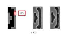
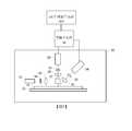
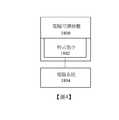
為更完全地理解本發明之本質及目的,應結合附圖參考下列[實施方式],其中:圖1係展示一正確建構(中心)及一缺陷(右邊)之一晶圓中之一圖案及相同圖案之影像之一設計表示的一例示性說明;圖2係將臨界構件定位於一設計檔案中之一例示性說明;圖3係用於收集一影像之一檢測系統之一圖式;圖4係展示儲存可執行於用於執行本發明之一電腦實施方法之一電腦系統上之程式指令之一非暫時性電腦可讀媒體的一圖式;圖5係無一設計交疊之一缺陷熱點之一例示性說明;圖6係具有一設計交疊之一缺陷熱點之一例示性說明;圖7係圖5之缺陷熱點中所識別之潛在缺陷之一例示性說明;圖8係圖6之缺陷熱點中所識別之潛在缺陷之一例示性說明,其中設計檔案交疊於該缺陷熱點上;圖9係基於缺陷熱點上之交疊之設計檔案而識別且分類成所關注之缺陷及滋擾缺陷之潛在缺陷的一例示性說明;及圖10係展示根據本發明之一實施例之一方法的一流程圖。In order to fully understand the essence and purpose of the present invention, the following [Embodiments] should be referred to in conjunction with the drawings, in which: Figure 1 shows a pattern and a pattern in a wafer with a correct construction (center) and a defect (right) An exemplary illustration of a design representation of an image of the same pattern; Fig. 2 is an exemplary illustration of positioning critical components in a design file; Fig. 3 is a diagram of a detection system used to collect an image; The 4 series shows a pattern of a non-transitory computer-readable medium that can be used to execute a program instruction on a computer system of a computer-implemented method of the present invention; Fig. 5 is a pattern without a design overlap and a defect An illustrative description of one of the hot spots; Fig. 6 is an exemplary description of a defect hot spot with a design overlap; Fig. 7 is an exemplary description of one of the potential defects identified in the defect hot spot of Fig. 5; Fig. 8 is shown in Fig. 6 An illustrative description of the potential defects identified in the defect hotspots, where the design files overlap the defect hotspots; Figure 9 is based on the overlapping design files on the defect hotspots, which are identified and classified into the defects and nuisances concerned. An illustrative description of the potential defect of the disturbance defect; andFig. 10 is a flowchart showing a method according to an embodiment of the present invention.
本申請案主張2016年6月29日申請之美國臨時申請案第62/356,499號(現處於待審中)之優先權,該案之揭示內容以引用的方式併入本文中。This application claims the priority of U.S. Provisional Application No. 62/356,499 (currently pending) filed on June 29, 2016, and the disclosure of this case is incorporated herein by reference.
儘管將根據特定實施例來描述所主張之標的物,但其他實施例(包含不提供本文中所闡述之全部優點及特徵的實施例)亦在本發明之範疇內。可在不背離本發明之範疇的情況下作出各種結構、邏輯、程序步驟及電子改變。相應地,僅參考隨附申請專利範圍來界定本發明之範疇。Although the claimed subject matter will be described in terms of specific embodiments, other embodiments (including embodiments that do not provide all the advantages and features described herein) are also within the scope of the present invention. Various structural, logical, program steps, and electronic changes can be made without departing from the scope of the present invention. Correspondingly, the scope of the present invention is defined only by referring to the scope of the attached patent application.
如本文中使用,術語「晶圓」一般係指由一半導體或非半導體材料形成之基板。此一半導體或非半導體材料之實例包含(但不限於)單晶矽、砷化鎵及磷化銦。此等基板通常可在半導體製造廠中找到及/或處理。As used herein, the term "wafer" generally refers to a substrate formed of a semiconductor or non-semiconductor material. Examples of such semiconductor or non-semiconductor materials include, but are not limited to, single crystal silicon, gallium arsenide, and indium phosphide. Such substrates can usually be found and/or processed in semiconductor manufacturing plants.
一晶圓可包含形成於一基板上之一或多層。例如,此等層可包括(但不限於)一光阻劑、一介電材料及一導電材料。技術中熟知諸多不同類型之此等層,且如本文中所使用之術語晶圓意欲涵蓋包含全部類型之此等層之一晶圓。A wafer may include one or more layers formed on a substrate. For example, these layers may include (but are not limited to) a photoresist, a dielectric material, and a conductive material. Many different types of these layers are well known in the art, and the term wafer as used herein is intended to cover a wafer that includes all types of these layers.
形成於一晶圓上之一或多層可係「經圖案化」或「未經圖案化」。例如,一晶圓可包含複數個晶粒,各晶粒具有可重複圖案化特徵。此等材料層之形成及處理最終可導致完成裝置。諸多不同類型的裝置(諸如積體電路(IC))可形成於一晶圓上,且如本文中使用之術語晶圓意欲涵蓋可在其上製造技術中熟知之任何類型之裝置的一晶圓。如本文中所使用,術語「晶片」可包括經設計用於一特定目的之IC之一集合。One or more layers formed on a wafer can be "patterned" or "unpatterned". For example, a wafer may include a plurality of dies, and each die has repeatable patterning features. The formation and processing of these material layers can ultimately lead to the completion of the device. Many different types of devices (such as integrated circuits (IC)) can be formed on a wafer, and the term wafer as used herein is intended to cover a wafer on which any type of device known in the manufacturing technology can be manufactured . As used herein, the term "chip" may include a collection of ICs designed for a specific purpose.
儘管本文中相對於晶圓描述若干實施例,但應瞭解,該等實施例可用於諸如一主光罩之另一樣本(其通常亦可指稱一遮罩或一光罩)。諸多不同類型之主光罩係技術中熟知的,且如本文所使用之術語「主光罩」、「遮罩」、「光罩」意欲涵蓋技術中熟知之全部類型之主光罩。Although several embodiments are described herein with respect to wafers, it should be understood that these embodiments mayUsed for another sample such as a main mask (which can also be often referred to as a mask or a mask). Many different types of main masks are well known in the art, and the terms "main mask", "mask", and "mask" as used herein are intended to cover all types of main masks known in the art.
偵測一晶圓上之缺陷可涉及使用一或多個光學器件模式,其包含使用該一或多個光學器件模式及一或多個缺陷偵測演算法來對該晶圓執行一熱掃描。一「熱掃描」一般係指一晶圓之一掃描/檢測,其經執行以藉由應用相對積極偵測設定(例如,實質上接近於雜訊底限之臨限值)來偵測該晶圓上之缺陷。依此方式,可執行熱掃描以收集將用於調諧處理程序(光學器件選擇及演算法調諧)之關於晶圓之檢測資料。熱掃描之目的在於:在(若干)選定模式中偵測晶圓上之全部缺陷及滋擾類型之一代表性樣本。Detecting defects on a wafer may involve using one or more optical device modes, which includes using the one or more optical device modes and one or more defect detection algorithms to perform a thermal scan on the wafer. A "thermal scan" generally refers to a scan/inspection of a wafer, which is executed to detect the wafer by applying relatively aggressive detection settings (for example, a threshold value that is substantially close to the noise floor). Defects in the circle. In this way, a thermal scan can be performed to collect inspection data about the wafer that will be used in the tuning process (optical device selection and algorithm tuning). The purpose of thermal scanning is to detect a representative sample of all defects and nuisance types on the wafer in (several) selected modes.
本文中所描述之實施例可包含多個熱掃描,例如,一熱掃描用於光學器件選擇,且另一熱掃描用於參數調諧。可使用經選擇用於晶圓檢測之(若干)光學模式來執行針對參數選擇執行之熱掃描。選擇(若干)光學模式可包含藉由總體計分來進行光學器件選擇,其在尋找DOI時自動計算指定光學器件模式之一模式或組合之「良好」程度之一單個數字同時抑制一給定缺陷集合之滋擾。此消除跨諸多模式逐缺陷手動地比較信雜比之工作,且顯著減小光學器件選擇時間。The embodiments described herein may include multiple thermal scans, for example, one thermal scan is used for optical device selection and another thermal scan is used for parameter tuning. The optical mode(s) selected for wafer inspection can be used to perform thermal scanning for parameter selection execution. Selecting the optical mode(s) may include selecting the optical device by overall scoring, which automatically calculates the "good" degree of one mode or combination of the specified optical device mode when looking for DOI. A single number while suppressing a given defect The nuisance of the assembly. This eliminates the work of manually comparing the signal-to-noise ratio defect by defect across many modes, and significantly reduces the optical device selection time.
本文中所描述之實施例可利用一組處理器節點,其等經組態以使用儲存於儲存媒體及用於晶圓之至少一額外資料源之陣列中之影像資料來產生該晶圓之一影像。依此方式,該組處理器節點可經組態以執行多通道影像融合。用於該晶圓之(若干)額外資料源可包含可在影像融合時獲得之任何資訊。此等資料源可包含(但不限於)設計資料、使用設計佈局來離線產生之一晶粒脈絡映射、自(若干)影像離線產生之一晶粒脈絡映射、缺陷偵測結果、由一檢測系統之不同偵測通道產生之影像資料所產生之缺陷偵測結果、由經由之多個(不同)掃描(使用檢測系統之不同成像模式來執行多個掃描)產生之影像資料、有關用於將圖案印刷於晶圓上之一主光罩之資訊等等。The embodiments described herein may utilize a set of processor nodes that are configured to use image data stored in a storage medium and an array of at least one additional data source for the wafer to generate one of the wafers image. In this way, the set of processor nodes can be configured to perform multi-channel image fusion. The additional data source(s) for the wafer may include any information that can be obtained during image fusion. These data sources may include (but are not limited to) design data, use of design layout to generate a grain context map offline, offline generation of a grain context map from (several) images, defect detectionTest results, defect detection results generated by image data generated by different detection channels of an inspection system, images generated by multiple (different) scans (using different imaging modes of the inspection system to perform multiple scans) Information, information about one of the main masks used to print the pattern on the wafer, etc.
影像融合可不包含簡單地交疊多個資料源(儘管亦可由本文中所描述之實施例執行此交疊)。相反,影像融合可包含組合多個資料源來產生一複合影像。亦可如Chen等人於2009年1月26日申請制共同擁有之美國專利申請案第12/359,476號中所描述,如2010年7月29日發表之美國專利申請公開案第2010/0188657號(其以引用的方式併入)般執行影像融合。Image fusion may not include simply overlapping multiple data sources (although this overlapping can also be performed by the embodiments described herein). In contrast, image fusion may include combining multiple data sources to produce a composite image. It can also be as described in the US Patent Application No. 12/359,476 jointly owned by Chen et al. on January 26, 2009, such as the US Patent Application Publication No. 2010/0188657 published on July 29, 2010 (It is incorporated by reference) generally performs image fusion.
在一實施例中,將由一主光罩檢測系統產生之一主光罩之一影像用作影像資料空間中之影像資料。依此方式,可將由一主光罩檢測系統產生之一主光罩之一影像用作影像資料之一替代。此實施例中所使用之該主光罩之該影像可包含由技術中熟知之任何主光罩檢測系統依任何適當方式產生之主光罩之任何適當影像。例如,該主光罩之該影像可為分別由一高放大率光學主光罩檢測系統或一基於電子束之主光罩檢測系統獲取之該主光罩之一高放大率光學或電子束影像。替代地,該主光罩之該影像可為由一空中成像主光罩檢測系統獲取之該主光罩之一空中影像。In one embodiment, an image of a main mask generated by a main mask detection system is used as the image data in the image data space. In this way, an image of a main mask generated by a main mask detection system can be used as a substitute for image data. The image of the main mask used in this embodiment may include any suitable image of the main mask produced by any main mask detection system known in the art in any suitable manner. For example, the image of the main mask may be a high-magnification optical or electron beam image of the main mask obtained by a high-magnification optical main mask detection system or an electron beam-based main mask detection system, respectively . Alternatively, the image of the main mask may be an aerial image of the main mask obtained by an aerial imaging main mask detection system.
術語「臨界區域」一般可界定為一使用者出於一些原因關注之晶圓上之區域且因此應被檢測。在當前所使用之臨界區域之一實例中,一晶圓之一層之臨界區域可經界定使得該等臨界區域包含形成於該層上之臨界構件且不包含形成於該層上之非臨界構件。一動態臨界區域係基於在一晶圓上執行之一檢測或自動缺陷檢視步驟以供相同晶圓上執行之一後續檢測或檢視步驟的結果而產生之一臨界區域。The term "critical region" can generally be defined as an area on a wafer that a user is concerned about for some reason and should therefore be inspected. In one example of the critical regions currently used, the critical regions of a layer of a wafer can be defined such that the critical regions include critical components formed on the layer and do not include non-critical components formed on the layer. A dynamic critical area is generated based on the result of performing an inspection or automatic defect inspection step on a wafer for a subsequent inspection or inspection step to be performed on the same wafer.
一種用於針對檢測判定臨界區域之方法包含:獲取由一第一檢測程序產生之一晶圓之檢測結果。獲取該等檢測結果可包含:實際上在該晶圓上執行該第一檢測程序(例如,藉由使用一檢測工具來掃描該晶圓且使用由該掃描產生之輸出來偵測該晶圓上之缺陷)。然而,獲取該等檢測結果可不包含執行該第一檢測程序。例如,獲取該等檢測結果可包含:自其中該等檢測結果已被另一方法或系統(例如,執行該第一檢測程序之另一方法或系統)儲存之一儲存媒體獲取該等檢測結果。該第一檢測程序可包含含有本文中將進一步描述之此等檢測程序之任何者的任何適當檢測程序。該第一檢測程序可包含:在產生檢測結果(諸如缺陷位置)之該第一檢測程序中執行一熱配方。該等檢測結果可包含可由一檢測程序產生之任何及全部檢測結果。A method for determining critical areas for inspection includes: obtaining inspection results of a wafer produced by a first inspection program. Obtaining the inspection results may include: actually executing the first inspection procedure on the wafer (for example, by using an inspection tool to scan the wafer and using the output generated by the scan to detect the wafer The defect). However, obtaining the detection results may not include executing the first detection procedure. For example, obtaining the detection results may include: obtaining the detection results from a storage medium in which the detection results have been stored by another method or system (for example, another method or system for executing the first detection procedure). The first detection program may include any suitable detection program that includes any of these detection programs described further herein. The first inspection procedure may include: executing a thermal recipe in the first inspection procedure that generates inspection results (such as defect locations). The test results can include any and all test results that can be produced by a test procedure.
可在已在該晶圓上執行一第一製造步驟之後且在已在該晶圓上執行一第二製造步驟之前在該晶圓上執行該第一檢測程序。如本文中所使用之一製造步驟一般係指涉及依一些物理、化學、機械等等之方式改變該晶圓之任何半導體製程。例如,一製造步驟可包含一微影程序、一蝕刻程序、一化學機械拋光程序及其類似者。在一此實例中,該第一製造步驟可為一微影程序,且該第二製造步驟可為一蝕刻程序。可在該晶圓上相繼執行該第一製造步驟及該第二步驟(例如,在不在該第一製造步驟與該第二製造步驟之間於該晶圓上執行任何其他製造步驟的情況下)。相比而言,不包含意外地改變一晶圓之可在該晶圓上執行之程序包含檢測及檢視程序。The first inspection procedure can be performed on the wafer after a first manufacturing step has been performed on the wafer and before a second manufacturing step has been performed on the wafer. As used herein, a manufacturing step generally refers to any semiconductor manufacturing process that involves changing the wafer in some physical, chemical, mechanical, and so on. For example, a manufacturing step may include a lithography process, an etching process, a chemical mechanical polishing process, and the like. In one example, the first manufacturing step may be a lithography process, and the second manufacturing step may be an etching process. The first manufacturing step and the second step can be performed successively on the wafer (for example, without performing any other manufacturing steps on the wafer between the first manufacturing step and the second manufacturing step) . In contrast, procedures that can be executed on a wafer that do not include accidentally changing a wafer include inspection and inspection procedures.
判定臨界區域亦可包含:基於該等檢測結果來針對一第二檢測程序判定臨界區域。將在已在該晶圓上執行該第二製造步驟之後在該晶圓上執行該第二檢測程序。判定該等臨界區域可包含:判定將被檢測之該晶圓上的位置或區域及將被用於偵測該等臨界區域之各者中之缺陷的一或多個檢測參數。針對一些臨界區域判定之該一或多個檢測參數可不同於針對其他臨界區域判定之一或多個檢測參數。例如,該方法允許一特定晶圓之選定區域中之一給定檢測步驟之靈敏度經定製成由一較早步驟中之一檢測在該特定晶圓上偵測到之雜訊及信號。換言之,該方法可利用來自一檢測步驟之檢測結果來增強或解諧一後續檢測步驟或(若干)步驟中之晶圓之靈敏度。依此方式,該方法可使在一製程之後執行之一檢測步驟與在下一或另一製程之後執行之一檢測步驟相關聯。Determining the critical area may also include: determining the critical area for a second detection procedure based on the detection results. The second inspection procedure will be performed on the wafer after the second manufacturing step has been performed on the wafer. Determining the critical areas may include: determining the wafer to be inspectedThe location or area of and one or more detection parameters that will be used to detect defects in each of these critical areas. The one or more detection parameters determined for some critical regions may be different from the one or more detection parameters determined for other critical regions. For example, the method allows the sensitivity of a given detection step in a selected area of a specific wafer to be customized to detect the noise and signal detected on the specific wafer by one of the earlier steps. In other words, the method can use the inspection results from one inspection step to enhance or detune the sensitivity of the wafer in a subsequent inspection step or step(s). In this way, the method can associate a detection step performed after a process with a detection step performed after the next or another process.
在多數半導體製造廠中,檢測配方相當冷地運行以在不影響產率之程序中提供具有小變動之結果之穩定性。藉由在一單一晶圓基礎上選擇性地增強區域中之靈敏度,吾人可基於自晶圓未放棄穩定性之一早前檢測記錄之信號來較佳偵測臨界區域中之缺陷。In most semiconductor manufacturing plants, the test formulation is run quite cold to provide stability with small changes in results in a procedure that does not affect the yield. By selectively enhancing the sensitivity in the area on a single wafer basis, we can better detect the defects in the critical area based on the signal recorded from the previous inspection and recording of the stability of the wafer.
使用一電腦系統(其可如本文中所描述般組態)來執行獲取檢測結果及判定臨界區域。A computer system (which can be configured as described in this article) is used to perform the acquisition of the detection result and the determination of the critical region.
為使本文中所描述之方案發揮其等最大潛能,應將臨界區域實質準確地對準至設計空間。Kulkarni等人共同擁有之美國專利案第7,676,077號中描述用於將設計空間對準至檢測或晶圓空間的方法及系統,該案如本文中所完全闡述以引用的方式併入。本專利中所描述之方法及系統之任何者可用於本文中所描述之方法中以將設計空間對準至檢測或晶圓空間,且反之亦然。In order to maximize the potential of the solution described in this article, the critical area should be accurately aligned to the design space. A method and system for aligning a design space to an inspection or wafer space is described in US Patent No. 7,676,077 jointly owned by Kulkarni et al., which is fully described herein and incorporated by reference. Any of the methods and systems described in this patent can be used in the methods described herein to align the design space to the inspection or wafer space, and vice versa.
在一實施例中,該等檢測結果包含雜訊事件、邊緣缺陷及偵測缺陷,且臨近區域經判定使得臨近該等臨界區域包含該等雜訊事件、該等邊緣缺陷及該等偵測缺陷之至少若干者的位置。雜訊事件一般可經界定為具有高於雜訊底限且比缺陷偵測臨限值更接近於雜訊底限之值的信號。邊緣缺陷一般可經界定為具有低於缺陷偵測臨限值且比雜訊底限更接近於缺陷偵測臨限值之值的信號。雜訊事件、邊緣缺陷及偵測缺陷之位置可用於判定後續檢測步驟之臨界區域之位置。依此方式,該方法可包含:利用來自一檢測步驟之檢測結果來藉由利用該第一步驟中之一缺陷或信號之空間位置而在一後續檢測步驟中敏化或減敏晶圓之檢測。In one embodiment, the detection results include noise events, edge defects, and detection defects, and the adjacent areas are determined such that the adjacent critical areas include the noise events, the edge defects, and the detection defects The location of at least a few of them. Noise events can generally be defined as havingThere are signals that are higher than the noise threshold and closer to the noise threshold than the defect detection threshold. An edge defect can generally be defined as a signal with a value lower than the defect detection threshold and closer to the defect detection threshold than the noise threshold. The location of noise events, edge defects, and detection defects can be used to determine the location of the critical area in subsequent inspection steps. In this way, the method may include: using the inspection result from an inspection step to sensitize or desensitize the inspection of the wafer in a subsequent inspection step by using the spatial position of a defect or signal in the first step.
可產生一運行時間脈絡映射(RTCM)且可如上文參考Kulkarni等人之專利中所描述般執行基於脈絡之檢測(CBI)。可如Zafar等人於2009年8月4日發佈之共同擁有之美國專利第7,570,796號中所描述般執行DBC,該案如本文中所完全闡述以引用的方式併入。A running time context map (RTCM) can be generated and context-based detection (CBI) can be performed as described in the patent by Kulkarni et al. above. The DBC can be implemented as described in jointly owned US Patent No. 7,570,796 issued by Zafar et al. on August 4, 2009, which is fully described herein and incorporated by reference.
在一些實施例中,該等檢測結果包含雜訊事件、邊緣缺陷及偵測缺陷。本發明之實施例可包含:針對該等雜訊事件、邊緣缺陷及偵測缺陷之至少若干者判定基於設計之資訊;及基於該基於設計之資訊來執行判定臨界區域。In some embodiments, the detection results include noise events, edge defects, and detection defects. Embodiments of the present invention may include: determining design-based information for at least some of the noise events, edge defects, and detection defects; and executing a critical region determination based on the design-based information.
在一實施例中,一檢測系統用於收集影像資料。例如,本文中所描述之光學及電子束輸出獲取子系統可經組態為檢測系統。在另一實施例中,影像資料獲取子系統係一缺陷檢視系統。例如,本文中所描述之光學及電子束輸出獲取子系統可經組態為缺陷檢視系統。在一進一步實施例中,該影像資料獲取子系統係一度量系統。例如,本文中所描述之光學及電子束輸出獲取子系統可經組態為度量系統。明確而言,可修改本文中所描述及圖3中所展示之輸出獲取子系統之實施例之一或多個參數來取決於將被使用之應用而提供不同成像能力。在一此實例中,圖3中所展示之影像資料獲取子系統可經組態以:若其將用於缺陷檢視或度量而非用於檢測,則其具有一較高解析度。換言之,圖3中所展示之影像資料獲取子系統之實施例描述一影像資料獲取子系統之一些一般組態及各種組態,可依熟悉技術者明白之數種方式來定製該影像資料獲取子系統以產生具有或多或少適用於不同應用之不同成像能力的輸出獲取子系統。In one embodiment, a detection system is used to collect image data. For example, the optical and electron beam output acquisition subsystems described herein can be configured as a detection system. In another embodiment, the image data acquisition subsystem is a defect inspection system. For example, the optical and electron beam output acquisition subsystem described herein can be configured as a defect inspection system. In a further embodiment, the image data acquisition subsystem is a measurement system. For example, the optical and electron beam output acquisition subsystems described herein can be configured as a metrology system. Specifically, one or more of the parameters of the embodiments of the output acquisition subsystem described herein and shown in FIG. 3 can be modified to provide different imaging capabilities depending on the application to be used. In one example, the image data acquisition subsystem shown in Figure 3 can be configured to: if it will be used for defect inspection or measurement rather than for inspectionIf measured, it has a higher resolution. In other words, the embodiment of the image data acquisition subsystem shown in FIG. 3 describes some general configurations and various configurations of an image data acquisition subsystem. The image data acquisition can be customized in several ways that those skilled in the art can understand. Subsystem to produce output acquisition sub-systems with different imaging capabilities more or less suitable for different applications.
本發明之系統及方法可利用經組態用於樣本(諸如晶圓及主光罩)之檢測、缺陷檢視及度量之輸出獲取子系統、缺陷檢視輸出獲取子系統及度量影像資料獲取子系統。例如,本文中所描述之實施例可經組態以使用掃描電子顯微法(SEM)及光學影像用於遮罩檢測、晶圓檢測及晶圓度量之目的。明確而言,本文中所描述之實施例可安裝於一電腦節點或電腦叢集(其係一影像資料獲取子系統之一組件或耦合至該影像資料獲取子系統)(諸如一寬頻電漿檢測器、一電子束檢測器或缺陷檢視工具、一遮罩檢測器、一虛擬檢測器等等)上。依此方式,本文中所描述之實施例可產生可用於包含(但不限於)晶圓檢測、遮罩檢測、電子束檢測及檢視、度量等等之各種應用的輸出。可基於圖3中所展示之輸出獲取子系統將針對其產生實際輸出之樣本而如上文所描述般修改該輸出獲取子系統之特性。The system and method of the present invention can utilize an output acquisition subsystem, a defect inspection output acquisition subsystem, and a measurement image data acquisition subsystem configured for inspection, defect inspection, and measurement of samples (such as wafers and main masks). For example, the embodiments described herein can be configured to use scanning electron microscopy (SEM) and optical imaging for mask inspection, wafer inspection, and wafer metrology purposes. Specifically, the embodiments described herein can be installed in a computer node or computer cluster (which is a component of an image data acquisition subsystem or is coupled to the image data acquisition subsystem) (such as a broadband plasma detector) , An electron beam detector or defect inspection tool, a mask detector, a virtual detector, etc.). In this way, the embodiments described herein can generate outputs that can be used in various applications including (but not limited to) wafer inspection, mask inspection, electron beam inspection and inspection, metrology, and so on. The characteristics of the output acquisition subsystem shown in FIG. 3 can be modified as described above based on the samples for which the output acquisition subsystem will produce actual output.
此一子系統包含含有至少一能源及一偵測器之一影像資料獲取子系統。該能源經組態以產生導引至一晶圓之能量。該偵測器經組態以自該晶圓偵測能量且回應於經偵測之能量而產生輸出。This subsystem includes an image data acquisition subsystem including at least one energy source and a detector. The energy is configured to generate energy directed to a wafer. The detector is configured to detect energy from the wafer and generate output in response to the detected energy.
在一實施例中,導引至該晶圓之該能量包含光,且自該晶圓偵測之該能量包含光。例如,在圖3中展示之系統之實施例中,影像資料獲取子系統10包含經組態以將光導引至晶圓14之一照明子系統。該照明子系統包含至少一光源。例如,如圖3中所展示,該照明子系統包含光源16。在一實施例中,照明子系統經組態以依一或多個入射角(其可包含一或多個斜角及/或一或多個法線角)將光引導至晶圓。例如,如圖3中所展示,來自光源16之光透過光學元件18且接著通過透鏡20導引至分束器21(其依一法線入射角將光導引至晶圓14)。該入射角可包含任何適當入射角,其可取決於(例如)該晶圓之特性而變化。In one embodiment, the energy directed to the wafer includes light, and the energy detected from the wafer includes light. For example, in the embodiment of the system shown in FIG. 3, the image
該照明子系統可經組態以在不同時間依不同入射角將光引導至該晶圓。例如,該影像資料獲取子系統可經組態以改變該照明子系統之一或多個元件之一或多個特性使得光可依一不同於圖3中所展示之入射角的入射角引導至該晶圓。在一此實例中,該影像資料獲取子系統可經組態以移動光源16、光學元件18及透鏡20使得光依一不同入射角導引至該晶圓。The illumination subsystem can be configured to direct light to the wafer at different times and at different angles of incidence. For example, the image data acquisition subsystem can be configured to change one or more characteristics of one or more components of the illumination subsystem so that light can be directed to an incident angle different from the incident angle shown in FIG. 3 The wafer. In this example, the image data acquisition subsystem can be configured to move the
在一些例項中,該影像資料獲取子系統可經組態以同時依一個以上入射角將光引導至該晶圓。例如,該照明子系統可包含一個以上照明通道,該等通道之一者可包含如圖3中所展示之光源16、光學元件18及透鏡20且該等照明通道之另一者(圖中未展示)可包含類似元件,其可經不同或相同組態,或可包含至少一光源且可包含一或多個組件(諸如本文所進一步描述之組件)。若此光與另一光同時引導至該晶圓,則依不同入射角引導至該晶圓之光之一或多個特性(例如,波長、偏光等等)可為不同的,使得依該等不同入射角自該晶圓之照明產生之光可在(若干)偵測器處彼此區別。In some examples, the image data acquisition subsystem can be configured to simultaneously direct light to the wafer at more than one incident angle. For example, the lighting subsystem may include more than one lighting channel, one of these channels may include the
在另一例項中,該照明子系統可僅包含一光源(例如,圖3中所展示之源16)且來自該光源之光可藉由該照明子系統之一或多個光學元件(圖中未展示)分離成不同光學路徑(例如,基於波長、偏光等等)。接著,該等不同光學路徑之各者中之光可引導至該晶圓。多個照明通道可經組態以同時或在不同時間(例如,當不同照明通道用於依序照明該晶圓時)將光引導至該晶圓。在另一例項中,相同照明通道可經組態以在不同時間藉由不同特性將光引導至該晶圓。例如,在一些例項中,光學元件18可組態為一光譜過濾器且該光譜過濾器之性質可依各種不同方式(例如,藉由交換該光譜過濾器)改變,使得不同波長之光可在不同時間引導至該晶圓。該照明子系統可具有技術中熟知之用於依序或同時將具有不同或相同特性之光依不同或相同入射角引導至該晶圓之任何其他適當組態。In another example, the lighting subsystem may include only one light source (for example, the
在一實施例中,光源16可包含一寬頻電漿(BBP)光源。依此方式,由該光源產生且引導至該晶圓之光可包含寬頻光。然而,該光源可包含任何其他適當光源(諸如一雷射)。該雷射可包含技術中熟知之任何適當雷射且可經組態以依任何適當波長或技術中熟知之波長產生光。另外,該雷射可經組態以產生單色或幾乎單色之光。依此方式,該雷射可為一窄頻雷射。該光源亦可包含依多個離散波長或波帶產生光之一多色光源。In one embodiment, the
來自光學元件18之光可藉由透鏡20聚焦至分束器21上。儘管透鏡20在圖3中展示為一單一折射光學元件,但應瞭解,實際上,透鏡20可包含組合地將光自該光學元件聚焦至晶圓之數個折射及/或反射光學元件。圖3中所展示及本文中所描述之照明子系統可包含任何其他適當光學元件(圖中未展示)。此等光學元件之實例包含(但不限於)(若干)偏光組件、(若干)光譜過濾器、(若干)空間過濾器、(若干)反射光學元件、(若干)變跡器、(若干)分束器、(若干)孔隙及其類似者,其可包含技術中熟知之任何此等適當光學元件。另外,該系統可經組態以基於將用於輸出獲取之照明之類型來修改該照明子系統之元件之一或多者。The light from the
該影像資料獲取子系統亦可包含經組態以引起光在該晶圓上掃描之一掃描子系統。例如,該影像資料獲取子系統可包含在輸出獲取期間晶圓14安置於其上之平台22。該掃描子系統可包含可經組態以移動該晶圓使得光可在該晶圓上掃描之任何適當機械及/或機器人總成(其包含平台22)。另外或替代地,該影像資料獲取子系統可經組態使得該影像資料獲取子系統之一或多個光學元件在該晶圓上執行光之某種掃描。該光可依任何適當方式於該晶圓上掃描。The image data acquisition subsystem may also include a scanning subsystem configured to cause light to scan on the wafer. For example, the image data acquisition subsystem can include wafers during
該影像資料獲取子系統進一步包含一或多個偵測通道。該一或多個偵測通道之至少一者包含一偵測器,其經組態以歸因於藉由該影像資料獲取子系統照明該晶圓而自該晶圓偵測光且回應於偵測之光而產生輸出。例如,圖3中展示之影像資料獲取子系統包含兩個偵測通道,一偵測通道由收集器24、元件26及偵測器28形成且另一偵測通道由收集器30、元件32及偵測器34形成。如圖3中所展示,該兩個偵測通道經組態以依不同收集角度收集且偵測光。在一些例項中,一偵測通道經組態以偵測鏡面反射之光,且另一偵測通道經組態以自該晶圓偵測非鏡面反射(例如散射、繞射等等)之光。然而,該等偵測通道之兩者或多者可經組態以自該晶圓偵測相同類型之光(例如,鏡面反射之光)。儘管圖3展示包含兩個偵測通道之影像資料獲取子系統之一實施例,但該影像資料獲取子系統可包含不同數個偵測通道(例如,僅一偵測通道或兩個或兩個以上偵測通道)。儘管該等收集器之各者在圖3中展示為單一折射光學元件,但應瞭解,該等收集器之各者可包含一或多個折射光學元件及/或一或多個反射光學元件。The image data acquisition subsystem further includes one or more detection channels. At least one of the one or more detection channels includes a detector configured to detect light from the wafer by illuminating the wafer by the image data acquisition subsystem and responding to the detection Measure the light and produce output. For example, the image data acquisition subsystem shown in FIG. 3 includes two detection channels, one detection channel is formed by
該一或多個偵測通道可包含技術中熟知之任何適當偵測器。例如,該等偵測器可包含光電倍增管(PMT)、電荷耦合裝置(CCD)及延時積分(TDI)攝影機。該等偵測器亦可包含技術中熟知之任何其他適當偵測器。該等偵測器亦可包含非成像偵測器或成像偵測器。依此方式,若該等偵測器係非成像偵測器,則該等偵測器之各者可經組態以偵測散射光之特定特性(諸如強度),但可不經組態以偵測依據成像平面內之位置而改變之此等特性。因而,由包含於該影像資料獲取子系統之該等偵測通道之各者中之該等偵測器之各者產生的輸出可為信號或資料,而非影像信號或影像資料。在此等例項中,一電腦子系統(諸如該系統之電腦子系統36)可經組態以自該等偵測器之非成像輸出產生該晶圓之影像。然而,在其他例項中,該等偵測器可組態為經組態以產生成像信號或影像資料之成像偵測器。因此,該系統可經組態以依數種方式產生本文中所描述之影像。The one or more detection channels may include any suitable detectors known in the art. For example, the detectors may include photomultiplier tubes (PMT), charge coupled devices (CCD), and time delay integration (TDI) cameras. The detectors may also include any other suitable detectors known in the art. The detectors may also include non-imaging detectors or imaging detectors. In this way, if these detectionsIf the detector is a non-imaging detector, each of these detectors can be configured to detect specific characteristics (such as intensity) of scattered light, but can be unconfigured to detect changes depending on the position in the imaging plane Of these characteristics. Therefore, the output generated by each of the detectors included in each of the detection channels of the image data acquisition subsystem may be a signal or data, rather than an image signal or image data. In these examples, a computer subsystem (such as the
應注意,本文中提供圖3以大體上繪示可包含於本文所描述之系統實施例中之一影像資料獲取子系統的一組態。顯然,如同通常在設計一工業用系統時執行,本文中所描述之影像資料獲取子系統組態可經改變以最佳化系統之效能。另外,可使用一既有輸出獲取系統(例如,藉由將本文中所描述之功能性添加至一既有輸出獲取系統)(諸如可自KLA-Tencor商購之工具)來實施本文中所描述之系統。針對一些此等系統,本文所描述之方法可提供為該輸出獲取系統之選用功能性(例如,除該輸出獲取系統之其他功能性之外)。替代地,本文所描述之系統可經「從頭開始」設計以提供一全新系統。It should be noted that FIG. 3 is provided herein to generally illustrate a configuration of an image data acquisition subsystem that can be included in the system embodiments described herein. Obviously, as usually performed when designing an industrial system, the configuration of the image data acquisition subsystem described in this article can be changed to optimize the performance of the system. In addition, an existing output acquisition system (for example, by adding the functionality described herein to an existing output acquisition system) (such as a tool commercially available from KLA-Tencor) can be used to implement the description herein的系统。 The system. For some of these systems, the methods described herein can provide optional functionality for the output acquisition system (for example, in addition to other functionality of the output acquisition system). Alternatively, the system described herein can be designed "from the ground up" to provide a completely new system.
該系統之電腦子系統36可依任何適當方式(例如,經由一或多個傳輸媒體,其可包含「有線」及/或「無線」傳輸媒體)耦合至該影像資料獲取子系統之該等偵測器,使得在該晶圓之掃描期間,該電腦子系統可接收由該等偵測器產生之輸出。電腦子系統36可經組態以使用如本文中所描述之偵測器之輸出來執行數個功能及本文中進一步描述之任何其他功能。此電腦子系統可如本文中描述般進一步組態。The
此電腦子系統(與本文所描述之其他電腦子系統)在本文中亦可稱為「(若干)電腦系統」。本文所描述之(若干)電腦子系統或(若干)系統之各者可採用各種形式,包含一個人電腦系統、影像電腦、主機電腦系統、工作站、網路設備、網際網路設備或其他裝置。一般而言,術語「電腦系統」可經廣義地界定以涵蓋具有執行來自一記憶體媒體之指令之一或多個處理器的任何裝置。(若干)電腦子系統或(若干)系統亦可包含技術中熟知之任何適當處理器(諸如一平行處理器)。另外,(若干)電腦子系統或(若干)系統可包含作為一分立或一網路工具之具有高速處理及軟體之一電腦平台。This computer subsystem (and other computer subsystems described in this article) may also be referred to as "computer system(s)" in this article. Each of the computer subsystem(s) or system(s) described in this article can take various forms, including a personal computer system, a video computer, a host computer system, a workstation, a network device, an Internet device, or other devices. Generally speaking, the term "computer system" can be broadly defined to encompass any device that has one or more processors that execute instructions from a memory medium. The computer subsystem(s) or system(s) may also include any suitable processor known in the art (such as a parallel processor). In addition, (several) computer subsystems or (several) systems may include a computer platform with high-speed processing and software as a discrete or a network tool.
若該系統包含一個以上電腦子系統,則不同電腦子系統可彼此耦合使得影像、資料、資訊、指令等等可發送於如本文中將進一步描述之電腦子系統之間。例如,電腦子系統36可由任何適當傳輸媒體(其可包含技術中熟知之任何適當有線及/或無線傳輸媒體)耦合至(若干)電腦子系統102。此等電腦子系統之兩者或多者亦可由一共用電腦可讀儲存媒體(圖中未展示)有效地耦合。If the system includes more than one computer subsystem, different computer subsystems can be coupled with each other so that images, data, information, commands, etc. can be sent between the computer subsystems as described further herein. For example, the
一額外實施例係關於儲存用於執行用於模式選擇及影像融合之一電腦實施方法之在一電腦系統上可執行之程式指令的一非暫時性電腦可讀取媒體。圖4中展示一此實施例。明確而言,如圖4中所展示,非暫時性電腦可讀媒體1800包含可在電腦系統1804上執行之程式指令1802。該電腦實施方法可包含本文所描述之(若干)任何方法之(若干)任何步驟。An additional embodiment relates to a non-transitory computer-readable medium storing program instructions executable on a computer system for executing a computer-implemented method for mode selection and image fusion. One such embodiment is shown in FIG. 4. Specifically, as shown in FIG. 4, the non-transitory computer-
實施諸如本文中所描述之方法的程式指令1802可儲存於電腦可讀媒體1800上。電腦可讀媒體可為儲存媒體,諸如一磁碟或光碟、一磁帶或技術中熟知之任何其他適當非暫時性電腦可讀媒體。
可依各種方式(包含(尤其)基於程序之技術、基於組件之技術及/或物件導向技術)之任一者實施該等程式指令。例如,可使用ActiveX控制項、C++物件、JavaBeans、微軟基礎類別(「MFC」)、SSE(資料流SIMD延伸)或所需之其他技術或方法實施該等程式指令。The program instructions can be implemented in any of a variety of ways (including (especially) program-based technology, component-based technology, and/or object-oriented technology). For example, ActiveX controls, C++ objects, JavaBeans, Microsoft Foundation Classes ("MFC"), SSE (Data Stream SIMD Extension), or other required technologies or methods can be used to implement these program instructions.
可根據本文中所描述之實施例之任何者組態電腦系統1804。The
本文中所揭示之系統及方法可藉由利用z層脈絡資訊來改善缺陷偵測靈敏度。可透過RTCM資料使用z層脈絡資訊。本文中所揭示之系統及方法在一逐核心基礎上實現滋擾抑制,其可在一成像電腦或系統中之任何其他電腦中依最小處理單元執行。The system and method disclosed in this article can improve defect detection sensitivity by using z-layer context information. The z-layer context information can be used through RTCM data. The system and method disclosed in this article implement nuisance suppression on a core-by-core basis, which can be executed as a minimum processing unit in an imaging computer or any other computer in the system.
在一實施例中,本文中所揭示之系統及方法嵌入z層資訊作為RTCM資料之部分且將資訊作為脈絡資訊傳遞至處理器。該處理器可處理此資訊用於區域分段(其導致較佳靈敏度)。In one embodiment, the system and method disclosed herein embed z-layer information as part of RTCM data and pass the information to the processor as context information. The processor can process this information for area segmentation (which results in better sensitivity).
可藉由組合多個設計層來產生Z層脈絡。提供具有操作(諸如生長及收縮)之工具且應用邏輯表達來產生脈絡可幫助使用者產生不同種類之z層脈絡。The Z-layer vein can be generated by combining multiple design layers. Providing tools with operations (such as growth and contraction) and applying logic expressions to generate contexts can help users generate different types of z-layer contexts.
在一些實施例中,處理器可計算設計屬性(諸如交疊百分比、與z層脈絡之水平/垂直距離)且將此等屬性用於滋擾抑制中。該處理器亦可在一子像素基礎上使用曲線擬合且定限一類比空間用於依一較高準確度計算該等設計屬性來計算缺陷大小。例如,可與熱點檢測同時使用本發明之系統及方法且仍實現較佳靈敏度及滋擾抑制。在一些情形中,可在滋擾資料之群組內識別致命缺陷或所關注之缺陷。In some embodiments, the processor may calculate design attributes (such as overlap percentage, horizontal/vertical distance from the z-layer vein) and use these attributes in nuisance suppression. The processor can also use curve fitting on a sub-pixel basis and limit an analog space for calculating the design attributes with a higher accuracy to calculate the defect size. For example, the system and method of the present invention can be used simultaneously with hot spot detection and still achieve better sensitivity and nuisance suppression. In some cases, fatal flaws or flaws of concern can be identified within the group of nuisance data.
在一些實施例中,此z層脈絡資訊可用於分段像素以減小雜訊或將不同臨限值用於脈絡之不同片段。由於z層資訊正經歷對準,所以處理器處無設計剪輯獲取附加項。將全部所需資訊建構於RTCM資料本身中。In some embodiments, this z-layer context information can be used to segment pixels to reduce noise or use different thresholds for different segments of the context. Since the z-layer information is undergoing alignment, the processorNo design clip to get additional items. Construct all required information in the RTCM data itself.
在一些實施例中,處理器可運算脈絡屬性且將其等用於方法(諸如用於額外滋擾抑制之基於設計之分級)中。In some embodiments, the processor can compute context attributes and use them in methods such as design-based classification for additional nuisance suppression.
本發明之一實施例可被描述為用於移除滋擾資料之一方法。該方法包括:在一處理器處接收對應於一晶圓之一設計檔案。該設計檔案具有一或多個z層。An embodiment of the present invention can be described as a method for removing nuisance data. The method includes: receiving a design file corresponding to a wafer at a processor. The design file has one or more z layers.
該方法進一步包括:在該處理器處接收該晶圓之一或多個臨界區域。圖2繪示一晶圓之一突顯臨界區域。圖5繪示自該晶圓之剩餘分段或與其分開之臨界區域。此可指稱一熱點臨界區域。該熱點臨界區域可在子像素對準之後用於檢測。在一些實施例中,相同地處理熱點臨界區域中之全部像素。同樣地,可相同地處理該熱點臨界區域中所偵測之全部缺陷。該晶圓之該等臨界區域可基於該設計檔案中之預定圖案或先前識別之晶圓或設計缺陷或缺陷區域。The method further includes receiving one or more critical regions of the wafer at the processor. Figure 2 shows a prominent critical area of a wafer. Figure 5 shows the critical area from or separated from the remaining segment of the wafer. This can be referred to as a hotspot critical area. This hot spot critical area can be used for detection after sub-pixel alignment. In some embodiments, all pixels in the hotspot critical area are processed the same. Similarly, all the defects detected in the critical area of the hot spot can be treated the same. The critical regions of the wafer can be based on predetermined patterns in the design file or previously identified wafers or design defects or defective regions.
該方法進一步包括:指示一影像資料獲取子系統擷取對應於該晶圓之該一或多個臨界區域之一或多個影像。該方法進一步包括:在該處理器處接收對應於該晶圓之該一或多個臨界區域之該一或多個影像中之一或多個潛在缺陷位置。例如,該等潛在缺陷位置可為該臨界區域內或該晶圓內之座標之一列表。替代一實體位置,該等潛在缺陷位置可對應於影像中之像素或半像素座標。圖7之像素圖中可見潛在缺陷位置之一列表之另一實例。The method further includes: instructing an image data acquisition subsystem to acquire one or more images corresponding to the one or more critical regions of the wafer. The method further includes: receiving one or more potential defect locations in the one or more images corresponding to the one or more critical regions of the wafer at the processor. For example, the potential defect locations can be a list of coordinates in the critical area or in the wafer. Instead of a physical location, the potential defect locations can correspond to pixel or half-pixel coordinates in the image. Another example of a list of potential defect locations can be seen in the pixel map of FIG. 7.
該方法進一步包括:使用該處理器來使該設計檔案與對應於該晶圓之該一或多個臨界區域之該一或多個缺陷位置對準。圖6中可見該設計檔案與該臨界區域之對準之一此實例。一旦對準,則該方法進一步包括:使用該處理器以基於各潛在缺陷位置及該對準之設計檔案之該一或多個z層來識別該一或多個潛在缺陷位置中之滋擾資料。圖8繪示交疊於對準之設計檔案之z層上之潛在缺陷位置。在此實例中,存在兩個z層。在一些實施例中,可提供z層之手動編輯以適應額外需求。生長六邊形、合併六邊形且可在設計檔案上提供如同「及」、「或」、「反或」等等之邏輯運算來產生z層脈絡。The method further includes using the processor to align the design file with the one or more defect locations corresponding to the one or more critical regions of the wafer. An example of the alignment between the design file and the critical area can be seen in FIG. 6. Once aligned, the method further includes: usingThe processor is used to identify the nuisance data in the one or more potential defect locations based on each potential defect location and the one or more z-layers of the aligned design file. Figure 8 shows the location of potential defects overlapped on the z-layer of the aligned design file. In this example, there are two z layers. In some embodiments, manual editing of the z-layer can be provided to meet additional requirements. Growing hexagons, merging hexagons, and providing logical operations such as "and", "or", "negative OR", etc. on the design file to generate z-layer context.
在一實施例中,該方法可進一步包括:使用該處理器來分析該設計檔案以基於預定設計規則來判定該晶圓之該一或多個臨界區域。可執行規則來產生脈絡遮罩。在一些實施例中,關於用於缺陷偵測之臨界區域依埃準確度來將該z層脈絡傳遞至該處理器。In one embodiment, the method may further include: using the processor to analyze the design file to determine the one or more critical regions of the wafer based on predetermined design rules. Rules can be executed to generate a context mask. In some embodiments, the z-layer context is transferred to the processor with respect to the critical area used for defect detection with an accuracy of angstroms.
該方法進一步包括:使用該處理器來自該一或多個潛在缺陷位置移除該識別之滋擾資料。圖9繪示在此特定實施例中當潛在缺陷位置未接近於該一或多個z層時如何被識別為滋擾資料。在另一實施例中,基於各潛在缺陷位置之位置是否接近於該對準之設計檔案之各z層中之圖案資料來識別滋擾資料。在又另一實施例中,基於子像素缺陷位置、交疊百分比、與該對準之設計檔案中之該一或多個z層之水平距離或垂直距離來識別該滋擾資料。The method further includes: using the processor to remove the identified nuisance data from the one or more potential defect locations. FIG. 9 illustrates how the potential defect location is identified as nuisance data when the location of the potential defect is not close to the one or more z-layers in this particular embodiment. In another embodiment, the nuisance data is identified based on whether the location of each potential defect location is close to the pattern data in each z-layer of the aligned design file. In yet another embodiment, the nuisance data is identified based on the position of the sub-pixel defect, the overlap percentage, and the horizontal distance or the vertical distance from the one or more z-layers in the aligned design file.
該方法可進一步包括:使用該處理器以基於該設計檔案及對應於該晶圓之該一或多個臨界區域之該一或多個影像來產生一合成影像。在此一實施例中,識別該一或多個潛在缺陷位置中之滋擾資料的步驟亦可基於該合成影像。The method may further include: using the processor to generate a composite image based on the design file and the one or more images corresponding to the one or more critical regions of the wafer. In this embodiment, the step of identifying the nuisance data in the one or more potential defect locations can also be based on the composite image.
該方法可進一步包括:使用該處理器以基於該設計檔案中之該一或多個z層來分段該晶圓之該一或多個臨界區域。The method may further include: using the processor to segment the one or more critical regions of the wafer based on the one or more z-layers in the design file.
圖10係繪示體現本發明之一方法100的一流程圖。方法100包括:接收對應於一晶圓之一設計檔案(101)。該設計檔案可對應於用於在該晶圓上重複之三個設計之該晶圓之一子集。可通過一電子連接(諸如一內部網路或網際網路)自一本地硬碟或自一遠端伺服器接收該設計檔案(101)。FIG. 10 shows a flowchart of a
方法100可進一步包括:分析該設計檔案以判定一或多個臨界區域(103)。一處理器可分析設計檔案(103)。可使用先前缺陷資料來判定或可基於先前資料來手動判定臨界區域。The
方法100可進一步包括:接收該晶圓之一或多個臨界區域(105)。可基於該分析之設計檔案(103)來接收該等臨界區域(105)。亦可自一本地硬碟、一遠端伺服器或經由一內部網路或網際網路接收該等臨界區域(105)。該等臨界區域可在該處理器處被接收(105)、儲存於本地儲存器中或儲存於RAM中供處理器使用。方法100可進一步包括:分段該晶圓之該一或多個臨界區域(107)。可該分段(107)可由該處理器執行。The
方法100可進一步包括:指示一影像資料獲取子系統擷取該晶圓之一或多個影像(109)。該等影像可具有該晶圓之該等分段之臨界區域。可在該晶圓之一熱掃描期間擷取該等影像。該處理器可接收該等影像中之一或多個潛在缺陷位置(111)。此等係潛在缺陷位置,此係因為該等影像可指示滋擾資料或一實際缺陷。The
方法100可進一步包括:使該設計檔案與該一或多個潛在缺陷位置對準(113)。在一實施例中,方法100可進一步包括:基於該設計檔案來產生一合成影像(115)。例如,該處理器可將該設計檔案中之一或多個z層交疊於由該影像資料獲取子系統擷取之該等影像上方。The
方法100可進一步包括:識別該一或多個潛在缺陷位置中之滋擾資料(117)。可使用該設計檔案來識別滋擾資料(117)。例如,若一潛在缺陷位置不與該設計檔案中之一特徵區域重疊,則其可為滋擾資料。上文揭示識別滋擾資料(117)之其他演算法及方法。The
方法100可進一步包括:自該一或多個潛在缺陷位置移除該識別之滋擾資料(119)。可自資料庫移除該識別之滋擾資料(119)或將其加旗標為滋擾資料使其未來不被分析。The
儘管已相對於一或多個特定實施例來描述本發明,但應瞭解,可在不背離本發明之精神及範疇之情況下做出本發明之其他實施例。因此,本發明被視為僅由隨附申請專利範圍及其合理解譯限定。Although the present invention has been described with respect to one or more specific embodiments, it should be understood that other embodiments of the present invention can be made without departing from the spirit and scope of the present invention. Therefore, the present invention is deemed to be limited only by the scope of the attached patent application and its compatible interpretation.
100‧‧‧方法100‧‧‧Method
101‧‧‧接收設計檔案101‧‧‧Receive design files
103‧‧‧分析設計檔案103‧‧‧Analysis and Design File
105‧‧‧接收一或多個臨界區域105‧‧‧Receive one or more critical regions
107‧‧‧分段一或多個臨界區域107‧‧‧Segment one or more critical regions
109‧‧‧指示一影像資料獲取子系統擷取一或多個影像109‧‧‧Instruct an image data acquisition subsystem to capture one or more images
111‧‧‧接收一或多個潛在缺陷位置111‧‧‧Receive one or more potential defect locations
113‧‧‧使設計檔案與一或多個潛在缺陷位置對準113‧‧‧Align the design file with one or more potential defect locations
115‧‧‧產生一合成影像115‧‧‧Generate a composite image
117‧‧‧識別滋擾資料117‧‧‧Identify nuisance data
119‧‧‧移除識別之滋擾資料119‧‧‧Remove identified nuisance data
Claims (18)
Translated fromChineseApplications Claiming Priority (4)
| Application Number | Priority Date | Filing Date | Title |
|---|---|---|---|
| US201662356499P | 2016-06-29 | 2016-06-29 | |
| US62/356,499 | 2016-06-29 | ||
| US15/600,784 | 2017-05-21 | ||
| US15/600,784US10304177B2 (en) | 2016-06-29 | 2017-05-21 | Systems and methods of using z-layer context in logic and hot spot inspection for sensitivity improvement and nuisance suppression |
Publications (2)
| Publication Number | Publication Date |
|---|---|
| TW201810482A TW201810482A (en) | 2018-03-16 |
| TWI730133Btrue TWI730133B (en) | 2021-06-11 |
Family
ID=60786349
Family Applications (1)
| Application Number | Title | Priority Date | Filing Date |
|---|---|---|---|
| TW106121738ATWI730133B (en) | 2016-06-29 | 2017-06-29 | Systems and methods of using z-layer context in logic and hot spot inspection for sensitivity improvement and nuisance suppression |
Country Status (7)
| Country | Link |
|---|---|
| US (1) | US10304177B2 (en) |
| JP (1) | JP6906044B2 (en) |
| KR (1) | KR102201122B1 (en) |
| CN (1) | CN109314067B (en) |
| IL (1) | IL263315B (en) |
| TW (1) | TWI730133B (en) |
| WO (1) | WO2018005132A1 (en) |
Families Citing this family (4)
| Publication number | Priority date | Publication date | Assignee | Title |
|---|---|---|---|---|
| US11320742B2 (en)* | 2018-10-31 | 2022-05-03 | Taiwan Semiconductor Manufacturing Company Ltd. | Method and system for generating photomask patterns |
| US11557031B2 (en)* | 2019-11-21 | 2023-01-17 | Kla Corporation | Integrated multi-tool reticle inspection |
| US11887296B2 (en)* | 2021-07-05 | 2024-01-30 | KLA Corp. | Setting up care areas for inspection of a specimen |
| KR102657751B1 (en)* | 2021-08-19 | 2024-04-16 | 주식회사 크레셈 | Board inspection method using a learning model |
Citations (2)
| Publication number | Priority date | Publication date | Assignee | Title |
|---|---|---|---|---|
| US20050004774A1 (en)* | 2003-07-03 | 2005-01-06 | William Volk | Methods and systems for inspection of wafers and reticles using designer intent data |
| US20080295048A1 (en)* | 2007-05-24 | 2008-11-27 | Youval Nehmadi | Inline defect analysis for sampling and SPC |
Family Cites Families (31)
| Publication number | Priority date | Publication date | Assignee | Title |
|---|---|---|---|---|
| US6215896B1 (en) | 1995-09-29 | 2001-04-10 | Advanced Micro Devices | System for enabling the real-time detection of focus-related defects |
| US20070131877A9 (en)* | 1999-11-29 | 2007-06-14 | Takashi Hiroi | Pattern inspection method and system therefor |
| JP2001331784A (en) | 2000-05-18 | 2001-11-30 | Hitachi Ltd | Defect classification method and device |
| WO2002015238A2 (en) | 2000-08-11 | 2002-02-21 | Sensys Instruments Corporation | Device and method for optical inspection of semiconductor wafer |
| US6918101B1 (en)* | 2001-10-25 | 2005-07-12 | Kla -Tencor Technologies Corporation | Apparatus and methods for determining critical area of semiconductor design data |
| EP1579274A4 (en) | 2002-07-12 | 2006-06-07 | Cadence Design Systems Inc | Method and system for context-specific mask inspection |
| US8041103B2 (en) | 2005-11-18 | 2011-10-18 | Kla-Tencor Technologies Corp. | Methods and systems for determining a position of inspection data in design data space |
| KR101665168B1 (en)* | 2005-11-18 | 2016-10-11 | 케이엘에이-텐코 코포레이션 | Methods and systems for utilizing design data in combination with inspection data |
| US7676077B2 (en)* | 2005-11-18 | 2010-03-09 | Kla-Tencor Technologies Corp. | Methods and systems for utilizing design data in combination with inspection data |
| US7570796B2 (en)* | 2005-11-18 | 2009-08-04 | Kla-Tencor Technologies Corp. | Methods and systems for utilizing design data in combination with inspection data |
| US7496874B2 (en)* | 2005-12-21 | 2009-02-24 | Inetrnational Business Machines Corporation | Semiconductor yield estimation |
| JP5427609B2 (en) | 2006-12-19 | 2014-02-26 | ケーエルエー−テンカー・コーポレーション | Inspection recipe creation system and method |
| US8194968B2 (en) | 2007-01-05 | 2012-06-05 | Kla-Tencor Corp. | Methods and systems for using electrical information for a device being fabricated on a wafer to perform one or more defect-related functions |
| US7962864B2 (en)* | 2007-05-24 | 2011-06-14 | Applied Materials, Inc. | Stage yield prediction |
| US8126255B2 (en)* | 2007-09-20 | 2012-02-28 | Kla-Tencor Corp. | Systems and methods for creating persistent data for a wafer and for using persistent data for inspection-related functions |
| US8223327B2 (en) | 2009-01-26 | 2012-07-17 | Kla-Tencor Corp. | Systems and methods for detecting defects on a wafer |
| WO2010090152A1 (en)* | 2009-02-04 | 2010-08-12 | 株式会社日立ハイテクノロジーズ | Semiconductor defect integrated projection method and defect inspection support apparatus equipped with semiconductor defect integrated projection function |
| US8559001B2 (en) | 2010-01-11 | 2013-10-15 | Kla-Tencor Corporation | Inspection guided overlay metrology |
| US8781781B2 (en) | 2010-07-30 | 2014-07-15 | Kla-Tencor Corp. | Dynamic care areas |
| US20120316855A1 (en)* | 2011-06-08 | 2012-12-13 | Kla-Tencor Corporation | Using Three-Dimensional Representations for Defect-Related Applications |
| US9087367B2 (en)* | 2011-09-13 | 2015-07-21 | Kla-Tencor Corp. | Determining design coordinates for wafer defects |
| US8826200B2 (en)* | 2012-05-25 | 2014-09-02 | Kla-Tencor Corp. | Alteration for wafer inspection |
| JP6255152B2 (en) | 2012-07-24 | 2017-12-27 | 株式会社日立ハイテクノロジーズ | Inspection device |
| US9189844B2 (en)* | 2012-10-15 | 2015-11-17 | Kla-Tencor Corp. | Detecting defects on a wafer using defect-specific information |
| US9311698B2 (en) | 2013-01-09 | 2016-04-12 | Kla-Tencor Corp. | Detecting defects on a wafer using template image matching |
| KR102019534B1 (en)* | 2013-02-01 | 2019-09-09 | 케이엘에이 코포레이션 | Detecting defects on a wafer using defect-specific and multi-channel information |
| US8984450B2 (en)* | 2013-03-14 | 2015-03-17 | Taiwan Semiconductor Manufacturing Company, Ltd. | Method and apparatus for extracting systematic defects |
| US9310320B2 (en)* | 2013-04-15 | 2016-04-12 | Kla-Tencor Corp. | Based sampling and binning for yield critical defects |
| US9183624B2 (en) | 2013-06-19 | 2015-11-10 | Kla-Tencor Corp. | Detecting defects on a wafer with run time use of design data |
| US9715725B2 (en) | 2013-12-21 | 2017-07-25 | Kla-Tencor Corp. | Context-based inspection for dark field inspection |
| US9401016B2 (en) | 2014-05-12 | 2016-07-26 | Kla-Tencor Corp. | Using high resolution full die image data for inspection |
- 2017
- 2017-05-21USUS15/600,784patent/US10304177B2/enactiveActive
- 2017-06-16JPJP2019500329Apatent/JP6906044B2/enactiveActive
- 2017-06-16KRKR1020197002114Apatent/KR102201122B1/enactiveActive
- 2017-06-16WOPCT/US2017/037934patent/WO2018005132A1/ennot_activeCeased
- 2017-06-16CNCN201780035591.8Apatent/CN109314067B/enactiveActive
- 2017-06-29TWTW106121738Apatent/TWI730133B/enactive
- 2018
- 2018-11-27ILIL263315Apatent/IL263315B/enactiveIP Right Grant
Patent Citations (2)
| Publication number | Priority date | Publication date | Assignee | Title |
|---|---|---|---|---|
| US20050004774A1 (en)* | 2003-07-03 | 2005-01-06 | William Volk | Methods and systems for inspection of wafers and reticles using designer intent data |
| US20080295048A1 (en)* | 2007-05-24 | 2008-11-27 | Youval Nehmadi | Inline defect analysis for sampling and SPC |
Also Published As
| Publication number | Publication date |
|---|---|
| JP2019527475A (en) | 2019-09-26 |
| US20180005367A1 (en) | 2018-01-04 |
| TW201810482A (en) | 2018-03-16 |
| KR20190014103A (en) | 2019-02-11 |
| IL263315A (en) | 2018-12-31 |
| JP6906044B2 (en) | 2021-07-21 |
| KR102201122B1 (en) | 2021-01-08 |
| CN109314067A (en) | 2019-02-05 |
| CN109314067B (en) | 2020-07-17 |
| US10304177B2 (en) | 2019-05-28 |
| WO2018005132A1 (en) | 2018-01-04 |
| IL263315B (en) | 2020-08-31 |
Similar Documents
| Publication | Publication Date | Title |
|---|---|---|
| US10670535B2 (en) | Automated pattern fidelity measurement plan generation | |
| KR102438824B1 (en) | Defect detection and recipe optimization for inspection of 3D semiconductor structures | |
| TWI726169B (en) | Systems, non-transitory computer-readable medium, and computer-implemented methods for detecting defects on a reticle | |
| TWI701427B (en) | System configured to detect defects on a specimen, method for detecting defects on a specimen and non-transitory computer-readable medium thereof | |
| KR102019534B1 (en) | Detecting defects on a wafer using defect-specific and multi-channel information | |
| TWI738780B (en) | Systems and methods for automatic correction of drift between inspection and design for massive pattern searching | |
| TWI611488B (en) | Tuning wafer inspection recipes using precise defect locations | |
| TWI667717B (en) | Outlier detection on pattern of interest image populations | |
| TWI778264B (en) | Performance monitoring of design-based alignment | |
| TW201629811A (en) | Determining coordinates for an area of interest on a specimen | |
| TWI730133B (en) | Systems and methods of using z-layer context in logic and hot spot inspection for sensitivity improvement and nuisance suppression | |
| US7728965B2 (en) | Systems and methods for inspecting an edge of a specimen | |
| US9702827B1 (en) | Optical mode analysis with design-based care areas | |
| CN111837227B (en) | System for determining a layer on which a detected defect is located on a wafer | |
| TW202316105A (en) | Setting up care areas for inspection of a specimen | |
| TWI861415B (en) | System and method for detecting defects and related non-transitory computer-readable medium | |
| TWI818170B (en) | Defect candidate generation for inspection | |
| TWI751329B (en) | High accuracy of relative defect locations for repeater analysis | |
| TW202141210A (en) | Determining metrology-like information for a specimen using an inspection tool |