TWI728348B - Light-emitting apparatus - Google Patents
Light-emitting apparatusDownload PDFInfo
- Publication number
- TWI728348B TWI728348BTW108113852ATW108113852ATWI728348BTW I728348 BTWI728348 BTW I728348BTW 108113852 ATW108113852 ATW 108113852ATW 108113852 ATW108113852 ATW 108113852ATW I728348 BTWI728348 BTW I728348B
- Authority
- TW
- Taiwan
- Prior art keywords
- light
- wavelength conversion
- emitting device
- conversion layer
- emitting
- Prior art date
Links
- 238000006243chemical reactionMethods0.000claimsdescription96
- 238000000605extractionMethods0.000description36
- 230000003287optical effectEffects0.000description31
- 238000010586diagramMethods0.000description25
- 230000008859changeEffects0.000description14
- 239000002245particleSubstances0.000description13
- 238000009792diffusion processMethods0.000description7
- 238000002310reflectometryMethods0.000description7
- OAICVXFJPJFONN-UHFFFAOYSA-NPhosphorusChemical compound[P]OAICVXFJPJFONN-UHFFFAOYSA-N0.000description6
- 238000006073displacement reactionMethods0.000description6
- 239000004973liquid crystal related substanceSubstances0.000description5
- 239000000463materialSubstances0.000description5
- 230000007423decreaseEffects0.000description4
- 238000009826distributionMethods0.000description4
- 238000005259measurementMethods0.000description4
- 239000003086colorantSubstances0.000description3
- 238000005286illuminationMethods0.000description3
- 230000009467reductionEffects0.000description3
- 239000004020conductorSubstances0.000description2
- 230000000875corresponding effectEffects0.000description2
- 238000004088simulationMethods0.000description2
- 238000010521absorption reactionMethods0.000description1
- 230000004075alterationEffects0.000description1
- 230000005540biological transmissionEffects0.000description1
- 230000001427coherent effectEffects0.000description1
- 239000012141concentrateSubstances0.000description1
- 230000002596correlated effectEffects0.000description1
- 230000003247decreasing effectEffects0.000description1
- 230000007613environmental effectEffects0.000description1
- 238000000034methodMethods0.000description1
- 230000004048modificationEffects0.000description1
- 238000012986modificationMethods0.000description1
- 238000010606normalizationMethods0.000description1
- 239000000049pigmentSubstances0.000description1
- 239000002096quantum dotSubstances0.000description1
- 238000002834transmittanceMethods0.000description1
- 239000012780transparent materialSubstances0.000description1
Images


Classifications
- H—ELECTRICITY
- H10—SEMICONDUCTOR DEVICES; ELECTRIC SOLID-STATE DEVICES NOT OTHERWISE PROVIDED FOR
- H10H—INORGANIC LIGHT-EMITTING SEMICONDUCTOR DEVICES HAVING POTENTIAL BARRIERS
- H10H20/00—Individual inorganic light-emitting semiconductor devices having potential barriers, e.g. light-emitting diodes [LED]
- H10H20/80—Constructional details
- H10H20/85—Packages
- H10H20/851—Wavelength conversion means
- H10H20/8515—Wavelength conversion means not being in contact with the bodies
- H—ELECTRICITY
- H10—SEMICONDUCTOR DEVICES; ELECTRIC SOLID-STATE DEVICES NOT OTHERWISE PROVIDED FOR
- H10H—INORGANIC LIGHT-EMITTING SEMICONDUCTOR DEVICES HAVING POTENTIAL BARRIERS
- H10H20/00—Individual inorganic light-emitting semiconductor devices having potential barriers, e.g. light-emitting diodes [LED]
- H10H20/80—Constructional details
- H10H20/85—Packages
- H10H20/851—Wavelength conversion means
- H10H20/8514—Wavelength conversion means characterised by their shape, e.g. plate or foil
- G—PHYSICS
- G02—OPTICS
- G02F—OPTICAL DEVICES OR ARRANGEMENTS FOR THE CONTROL OF LIGHT BY MODIFICATION OF THE OPTICAL PROPERTIES OF THE MEDIA OF THE ELEMENTS INVOLVED THEREIN; NON-LINEAR OPTICS; FREQUENCY-CHANGING OF LIGHT; OPTICAL LOGIC ELEMENTS; OPTICAL ANALOGUE/DIGITAL CONVERTERS
- G02F1/00—Devices or arrangements for the control of the intensity, colour, phase, polarisation or direction of light arriving from an independent light source, e.g. switching, gating or modulating; Non-linear optics
- G02F1/01—Devices or arrangements for the control of the intensity, colour, phase, polarisation or direction of light arriving from an independent light source, e.g. switching, gating or modulating; Non-linear optics for the control of the intensity, phase, polarisation or colour
- G02F1/13—Devices or arrangements for the control of the intensity, colour, phase, polarisation or direction of light arriving from an independent light source, e.g. switching, gating or modulating; Non-linear optics for the control of the intensity, phase, polarisation or colour based on liquid crystals, e.g. single liquid crystal display cells
- G02F1/133—Constructional arrangements; Operation of liquid crystal cells; Circuit arrangements
- G02F1/1333—Constructional arrangements; Manufacturing methods
- G02F1/1335—Structural association of cells with optical devices, e.g. polarisers or reflectors
- G02F1/1336—Illuminating devices
- G02F1/133602—Direct backlight
- G02F1/133606—Direct backlight including a specially adapted diffusing, scattering or light controlling members
- G02F1/133607—Direct backlight including a specially adapted diffusing, scattering or light controlling members the light controlling member including light directing or refracting elements, e.g. prisms or lenses
- G—PHYSICS
- G02—OPTICS
- G02F—OPTICAL DEVICES OR ARRANGEMENTS FOR THE CONTROL OF LIGHT BY MODIFICATION OF THE OPTICAL PROPERTIES OF THE MEDIA OF THE ELEMENTS INVOLVED THEREIN; NON-LINEAR OPTICS; FREQUENCY-CHANGING OF LIGHT; OPTICAL LOGIC ELEMENTS; OPTICAL ANALOGUE/DIGITAL CONVERTERS
- G02F1/00—Devices or arrangements for the control of the intensity, colour, phase, polarisation or direction of light arriving from an independent light source, e.g. switching, gating or modulating; Non-linear optics
- G02F1/01—Devices or arrangements for the control of the intensity, colour, phase, polarisation or direction of light arriving from an independent light source, e.g. switching, gating or modulating; Non-linear optics for the control of the intensity, phase, polarisation or colour
- G02F1/13—Devices or arrangements for the control of the intensity, colour, phase, polarisation or direction of light arriving from an independent light source, e.g. switching, gating or modulating; Non-linear optics for the control of the intensity, phase, polarisation or colour based on liquid crystals, e.g. single liquid crystal display cells
- G02F1/133—Constructional arrangements; Operation of liquid crystal cells; Circuit arrangements
- G02F1/1333—Constructional arrangements; Manufacturing methods
- G02F1/1335—Structural association of cells with optical devices, e.g. polarisers or reflectors
- G02F1/1336—Illuminating devices
- G02F1/133614—Illuminating devices using photoluminescence, e.g. phosphors illuminated by UV or blue light
Landscapes
- Led Device Packages (AREA)
- Physics & Mathematics (AREA)
- Nonlinear Science (AREA)
- Planar Illumination Modules (AREA)
- Mathematical Physics (AREA)
- Chemical & Material Sciences (AREA)
- Crystallography & Structural Chemistry (AREA)
- General Physics & Mathematics (AREA)
- Optics & Photonics (AREA)
Abstract
Description
Translated fromChinese本發明是關於一個發光組件,特別是關於一個具有一發光元件與一光學元件的發光組件。The present invention relates to a light-emitting component, in particular to a light-emitting component having a light-emitting element and an optical element.
使用發光二極體(light-emitting diode;LED)的發光裝置因為具有節能、環保、使用壽命長以及體積小等優點,正逐漸地取代傳統白熾光源。Light-emitting devices using light-emitting diodes (LEDs) are gradually replacing traditional incandescent light sources because they have the advantages of energy saving, environmental protection, long service life, and small size.
數種的發光元件,例如透鏡、反射裝置以及波長轉換器,可以被用來改變發光裝置的光學特性。透鏡可以用來收集或者重新分配從發光二極體發出的光線。反射器可以將發光二極體發出的光線重新導向需要的方向。不僅如此,波長轉換器,例如螢光粉、顏料或者量子點材料,可以將發光二極體發出的光線轉換成別的顏色。Several types of light-emitting elements, such as lenses, reflective devices, and wavelength converters, can be used to change the optical characteristics of the light-emitting device. The lens can be used to collect or redistribute the light emitted from the light-emitting diode. The reflector can redirect the light emitted by the light-emitting diode to the desired direction. Not only that, wavelength converters, such as phosphors, pigments, or quantum dot materials, can convert light emitted by light-emitting diodes into other colors.
一發光裝置,具有一下表面、一發光二極體與一透明層。發光二極體具有一第一側表面與一相對於下表面的第一上表面,透明層覆蓋第一上表面並具有第二上表面與第二側表面。其中,該發光裝置具有一色度空間均勻性小於0.005。A light emitting device has a bottom surface, a light emitting diode and a transparent layer. The light emitting diode has a first side surface and a first upper surface opposite to the lower surface. The transparent layer covers the first upper surface and has a second upper surface and a second side surface. Wherein, the light-emitting device has a spatial uniformity of chromaticity less than 0.005.
一背光模組,具有一發光裝置,發光裝置具有一色度空間均勻性落在四個麥克亞當橢圓內。發光裝置具有一下表面、一發光二極體、一波長轉換層與一透明蓋。發光二極體具有一相對於下表面的第一上表面,波長轉換層覆蓋第一上表面,而透明蓋覆蓋波長轉換層並具有一第二上表面。A backlight module has a light-emitting device, and the light-emitting device has a spatial uniformity of chromaticity falling within four McAdam ellipses. The light emitting device has a bottom surface, a light emitting diode, a wavelength conversion layer and a transparent cover. The light emitting diode has a first upper surface opposite to the lower surface, the wavelength conversion layer covers the first upper surface, and the transparent cover covers the wavelength conversion layer and has a second upper surface.
1000A、1000B、1000C、1000D、1000E、1000F、1000G、1000H、2000A、2000B、2000C、2000D、2000E、2000F、3000、4000、5000、6000、8000:發光裝置1000A, 1000B, 1000C, 1000D, 1000E, 1000F, 1000G, 1000H, 2000A, 2000B, 2000C, 2000D, 2000E, 2000F, 3000, 4000, 5000, 6000, 8000: light emitting device
1003A、1007A、1007C、1007E、1008A、1008C、1008D、1009B:發光組件1003A, 1007A, 1007C, 1007E, 1008A, 1008C, 1008D, 1009B: light-emitting components
2:發光二極體2: Light-emitting diode
3:粒子3: particles
4、40、42、44、46、48、50、52:波長轉換層4. 40, 42, 44, 46, 48, 50, 52: wavelength conversion layer
6:透明層6: Transparent layer
8:透明蓋8: Transparent cover
10:載板10: Carrier board
18:擴散層18: Diffusion layer
20:稜鏡層20: 稜鏡 layer
22:LCD模組22: LCD module
24:光譜儀24: Spectrometer
100:上表面100: upper surface
120、122:導體部120, 122: Conductor part
140、142:側壁140, 142: side wall
160、162、164、166、170a、170b、172、174、176、180、184:透鏡160, 162, 164, 166, 170a, 170b, 172, 174, 176, 180, 184: lens
1740、1840:孔穴1740, 1840: holes
1760、1762:翼部1760, 1762: Wings
178a、178b:光圈178a, 178b: aperture
180:雙凸透鏡180: biconvex lens
θ1、θ2:角度θ1, θ2: angle
L1、L2:光線L1, L2: light
E1、E2:邊緣E1, E2: Edge
S1、S2:表面S1, S2: surface
U、U’:均勻度U, U’: uniformity
為讓本發明之上述和其他目的、特徵和優點能更明顯易懂,下文特舉實施例,並配合所附圖式,說明如下。In order to make the above and other objects, features and advantages of the present invention more comprehensible, the following embodiments are specifically cited in conjunction with the accompanying drawings, which are described as follows.
第1A~1H圖顯示本發明實施例中發光裝置之示意圖。Figures 1A to 1H show schematic diagrams of the light-emitting device in an embodiment of the present invention.
第2A~2D圖顯示本發明實施例中發光裝置的光學特性示意圖。Figures 2A to 2D show schematic diagrams of optical characteristics of the light-emitting device in an embodiment of the present invention.
第3A圖顯示本發明實施例中發光組件之示意圖。Figure 3A shows a schematic diagram of a light-emitting component in an embodiment of the present invention.
第3B~3C圖顯示本發明實施例中的結構圖。Figures 3B to 3C show the structural diagrams in the embodiment of the present invention.
第3D~3E圖顯示本發明實施例中發光組件的光學特性示意圖。Figures 3D to 3E show schematic diagrams of optical characteristics of the light-emitting component in an embodiment of the present invention.
第4A~4B圖顯示本發明實施例中的結構圖。Figures 4A to 4B show the structural diagrams in the embodiment of the present invention.
第4C~4F圖顯示本發明實施例中發光組件的結構與光學特性示意圖。Figures 4C to 4F show schematic diagrams of the structure and optical characteristics of the light-emitting component in an embodiment of the invention.
第5A~5C圖顯示本發明實施例中發光裝置之示意圖。Figures 5A to 5C show schematic diagrams of the light-emitting device in an embodiment of the present invention.
第6A~6F圖顯示本發明實施例中發光裝置之示意圖。Figures 6A to 6F show schematic diagrams of the light-emitting device in an embodiment of the present invention.
第7A~7J圖顯示本發明實施例中發光組件的示意圖與相關的光學特性。Figures 7A-7J show schematic diagrams and related optical characteristics of the light-emitting component in an embodiment of the present invention.
第8A~8D圖顯示本發明實施例中發光組件之示意圖。Figures 8A to 8D show schematic diagrams of light-emitting components in an embodiment of the present invention.
第9A~9D圖顯示本發明實施例中發光組件之示意圖。Figures 9A-9D show schematic diagrams of light-emitting components in an embodiment of the present invention.
第10A~10D圖顯示根據本發明一實施例的發光組件的示意圖。Figures 10A to 10D show schematic diagrams of a light-emitting component according to an embodiment of the invention.
第11A~11H圖顯示根據本發明一實施例的發光組件的示意圖及相關的光學特性。Figures 11A-11H show schematic diagrams and related optical characteristics of a light-emitting component according to an embodiment of the present invention.
第12A~12E圖所顯示的是根據本發明一實施例的量測設備與相關的結果。Figures 12A to 12E show the measurement equipment and related results according to an embodiment of the present invention.
第13圖所顯示的是根據本發明一實施例的發光組件的示意圖。Figure 13 shows a schematic diagram of a light-emitting assembly according to an embodiment of the present invention.
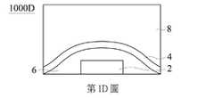
第1A圖顯示本發明一實施例中一發光裝置1000A之示意圖。發光裝置1000A包括一發光二極體2以及一波長轉換層4直接形成於發光二極體2之上,並環繞發光二極體2。發光裝置1000B具有一透明層6形成於波長轉換層4與發光二極體2之間。透明層6覆蓋發光二極體2的上表面與側表面,並側向地延伸到發光裝置1000B的邊緣。因此,發光二極體2與波長轉換層4被透明層6所隔開。FIG. 1A shows a schematic diagram of a light-emitting
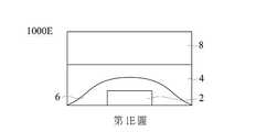
發光裝置1000C具有一透明蓋8形成於波長轉換層4之上。發光裝置1000D具有一透明蓋8、一個波長轉換層4、一個透明層6與一個發光二極體2由上往下依序堆疊。發光裝置1000D的波長轉換層4具有一下表及一上表面。下表面的輪廓與透明層6的上表面輪廓一致或者近似。上表面的輪廓與透明蓋8的上表面輪廓一致或相近。此外,波長轉換裝層4的上下表面可以有相同或者不同的輪廓。發光裝置1000D的波長轉換層4具有兩個彼此互相平行的表面(上表面及下表面)。發光裝置1000E的波長轉換層4形成於透明層6之上,並具有一下表面接近透明層6。波長轉換層4的下表面具有一與透明層6的上表面相同或者相似的輪廓,而波長轉換層4的上表面則具有一平坦的輪廓,或者是平行於發光裝置1000E或透明蓋8的上表面。發光裝置1000E的波長轉換層4具有一下表面及一平坦的上表面,其中,下表面大致沿著發光二極體2的輪廓延伸。The
發光裝置1000F具有一透明層6覆蓋發光二極體2的上表面與複數個側表面,於一個實施例中,透明層6的各個外表面都各自與相對應的內表面相互平行。換句話說,透明層6具有一致的厚度。The light-emitting
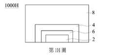
發光裝置1000G具有一個覆蓋發光二極體2的上表面與多個側表面的透明層6。一波長轉換層4覆蓋透明層6的上表面與多個側表面。一剖面形狀為矩形的透明蓋8則是形成在波長轉換層4的上表面。波長轉換層4具有一位於發光二極體2上方的上方厚度及位於發光二極體2側面的側向厚度。側向厚度大於上方厚度。The
發光二極體2具有一個主動層以發出一非同調性光。從發光二極體2發出的光具有第一光強度、第一光場與第一顏色。波長轉換層4具有一波長轉換材料,而波長轉換材料的粒子尺寸介於8~50μm,例如8、17、20、32或46μm。粒子尺寸可以是指粒子的半徑或者特徵長度。透明層6與透明蓋8具有透明材料,發光二極體2發出光線的至少60%可以穿過透明層6或者透明蓋8而不會被吸收,也就是說,透明層6或透明蓋8相對於發光二極體2發出的光線具有60%的透光率。發光裝置1000A~1000H可以發出一個具有第二光強度、第二光場與第二顏色的光線。第二光強度小於第一光強度,因為部分從發光二極體發出的光線在波長轉換層4、透明層6或者透明蓋8中被吸收或者被困住(trapped)。第二光場可以跟第一光場相同或者不同。藉由加入擴散粒子到透明層6或者透明蓋8可以散射光線及改變光場。於前述諸實施例中,光線的路徑可以藉由使用適當的模擬模型進而重現,例如蒙地卡羅光線追跡法(Monte Carlo ray tracing method)。光線在波長轉換層4內的傳遞也可以使用根據米氏散射理論(Mie Scattering theory)的模擬模型來重現。The
參考第1B與1D圖,透明層6具有一彎曲的輪廓。這個彎曲的輪廓在發光二極體2的上表面彎曲地凸起。波長轉換層4形成在透明層6的彎曲上表面上,因此具有一個內凹的下表面。透明層6更具有一輪廓近似於發光二極體2輪廓的下表面。參考第1F、1G與1H圖,透明層6與波長轉換層4大致上都有一個倒U(reversed-U)的形狀。參考第1H圖,透明蓋8也具有倒U的形狀。這個倒U的形狀具有一個上部(與一個側部,其中側部比上部薄。Referring to FIGS. 1B and 1D, the
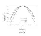
第2A~2D圖顯示本發明實施例中發光裝置的光學特性。第2A圖所顯示的是發光裝置1000A~1000H的光萃取效率(Light Extraction Efficiency)。這些光萃取效率介於100~140 lm/W。而發光裝置1000F具有最佳的光萃取效率。第2B圖所顯示的是發光裝置1000A~1000H於+90°~-90°的光場的色溫變化。這些變化介於100~450K。第2C~2D圖顯示以兩種不同單位表示各角度上的顏色變化,其中△u’ v’介於0.001~0.009,而△y則是介於0.01~0.1之間。Figures 2A to 2D show the optical characteristics of the light-emitting device in the embodiment of the present invention. Figure 2A shows the light extraction efficiency of the light-emitting
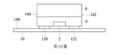
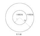
第3A圖顯示一具有本發明中一實施例的發光組件1003A的結構。發光組件1003A具有一發光裝置1000C經由導體部120與122形成於載板10的上表面100之上。發光組件1003A的側壁140與142可以是可以散射光線的Lambertian散射表面,如第3B圖所示。上表面100可以是一個具有90%反射率與10%吸收率的表面,或者是可以散射光線的Lambertian表面,如第3C圖所示。第3D圖所顯示的是八個發光組件(發光裝置1000A~1000H)在+90°~-90°之間顏色隨角度改變的程度,其中八個發光組件具有不同的上表面100及側壁142型態。參考第3D圖,當這個結構的側壁是Lambertian散射表面的時候,這個結構所提供的色彩空間均勻度(color space uniformity)比側壁是平坦的表面時來的差。FIG. 3A shows the structure of a light-emitting component 1003A according to an embodiment of the present invention. The light-emitting assembly 1003A has a light-emitting
第3E圖所顯示的是這八個具有不同上表面100與側壁140的發光組件的光萃取效率。而每一個發光組件都在四種不同的條件下量測。第一種條件是上表面100為Lambertian散射表面,而側壁140與142是平面。第二種條件是上表面100、側壁140與142都是Lambertian散射表面。第三種條件是上表面100為一個反射表面,而側壁140與142是平面,其中上表面100對於來自發光二極體的光線的反射率為90%。第四種條件是上表面100為反射面,而側壁140與142是Lambertian散射表面。根據第3D~3E圖,具有發光裝置1000F的發光組件以及具有發光裝置1000B的發光組件在同樣的條件下具有大於130 lm/W的發光效率,以及色溫差異低於0.04。FIG. 3E shows the light extraction efficiency of the eight light-emitting components with different
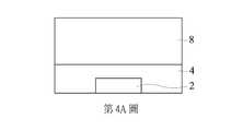
第4A~4B圖所顯示的是本發明中實施例的兩個結構。當第4A與4B圖中的波長轉換層的厚度增加時,兩個結構的發光效率都增加了,空間內的顏色均勻度也增加了,而兩個結構的色溫均勻度也增加了。不僅如此,波長轉換層4的厚度增加,對於第4B圖中的結構具有更明顯的影響。更具體地來說,當波長轉換層4的厚度由100μm增加到300μm的時候,第4B圖的結構的光萃取效率增加了4.89%、△CCT從486K降低到128K,以及△u’ v’從0.0088降到0.002。當波長轉換層4的厚度由100μm增加到400μm的時候,而第4A圖的結構的發光效率增加了10.97%、△CCT從529K降低到289K,以及△u’ v’從0.0089降到0.0055。然而,第4B圖中的結構僅需要增加較少的波長轉換層4的厚度,就能夠得到與第4A圖的結構大致相同的光學特性。Figures 4A to 4B show two structures of the embodiment of the present invention. When the thickness of the wavelength conversion layer in Figures 4A and 4B increases, the luminous efficiency of the two structures increases, the color uniformity in the space also increases, and the color temperature uniformity of the two structures also increases. Not only that, the increase in the thickness of the
第4C~4F圖顯示是本發明中實施例的結構與光學特性。在4D~4F圖中,橫坐標代表了光學特性,例如光萃取效率、色溫變化△CCT與色度空間均勻性△u’ v’。而橫坐標代表,如第4C圖中,發光二極體2與波長轉換層4之間的寬度W。當高度H從50μm增加到350μm,寬度W從50μm增加到350μm,光萃取效率從135 lm/W增加了約7.53%,如第4D圖所示。如第4F圖所示,色度空間均勻性△u’ v’從0.02降到低於0.01,大約是降低了34.8%。如第4E圖所示,色溫變化△CCT從1100K左右降到低於500K。當高度H大於250μm的時候,光萃取效率可以顯著的提升。當高度H是50μm以及寬度W為150μm的時候,色度空間均勻性△u’ v’大約為0.01。如第4F圖所示,若高度H等於50μm且寬度W介於50μm到250μm之間,也就是寬度W與高度H的比值不大於5的情況下,色度空間均勻性△u’ v’小於0.005。若高度H等於150μm且寬度W介於150μm到250μm之間,也就是寬度W與高度H的比值不大於(5/3)的情況下,色度空間均勻性△u’ v’也小於0.005。Figures 4C to 4F show the structure and optical characteristics of the embodiment of the present invention. In the 4D~4F graphs, the abscissa represents optical characteristics, such as light extraction efficiency, color temperature change ΔCCT, and chromaticity spatial uniformity Δu' v'. The abscissa represents the width W between the light-emitting
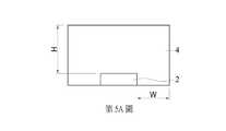
第第5A~5C圖顯示本發明實施例中的結構圖。參考第5A圖中的結構,當高度H大約是750μm以及發光裝置的尺寸大約是2X2mm2的時候,光萃取效率大於135 lm/W、色度空間均勻性△u’ v大約是0.04,以及色溫變化△CCT大約是200K。第5A圖中的發光裝置在高度H是350μm以及發光裝置的尺寸大約是1X1mm2的情況下,或者高度H是450μm以及發光裝置的尺寸大約是1.2X1.2mm2的情況下,可以具有更好的光學特性,例如光萃取效率、色度空間均勻性△u’ v’以及色溫變化△CCT。Figures 5A to 5C show the structural diagrams in the embodiment of the present invention. Referring to the structure in Figure 5A, when the height H is about 750μm and the size of the light-emitting device is about 2X2mm2 , the light extraction efficiency is greater than 135 lm/W, the chromaticity space uniformity △u'v is about 0.04, and the color temperature The change △CCT is about 200K. A light emitting device of FIG. 5A in the height dimension H is approximately 350μm and the light emitting device is a case where 1X1mm2, or the height dimension H is approximately 450μm and the light emitting device of the case 1.2X1.2mm2, may have a better The optical properties of, such as light extraction efficiency, chromaticity spatial uniformity △u'v' and color temperature change △CCT.
參考第5B圖的結構,當高度H是750μm以及發光裝置的尺寸大約是1.8X1.8mm2的情況下,色度空間均勻性△u’ v大約是0.02,色溫變化△CCT大約是100K。光萃取效率在高度H是750μm以及發光裝置的尺寸大約是2X2mm2的情況時,大於135 lm/W。而第5B圖中的發光裝置,在高度H是350μm以及發光裝置的尺寸大約是1.2X1.2mm2的情況下,或者高度H是450μm以及發光裝置的尺寸大約是1.2X1.2mm2的情況下時,會有更好的光學特性,例如光萃取效率、色度空間均勻性△u’ v’以及色溫變化△CCT。Referring to the structure in Figure 5B, when the height H is 750 μm and the size of the light-emitting device is about 1.8×1.8 mm2 , the chromaticity spatial uniformity Δu'v is about 0.02, and the color temperature change ΔCCT is about 100K. The light extraction efficiency is greater than 135 lm/W when the height H is 750 μm and the size of the light-emitting device is approximately2×2 mm 2. The light-emitting device in Figure 5B, when the height H is 350 μm and the size of the light-emitting device is approximately 1.2X1.2mm2 , or the height H is 450 μm and the size of the light-emitting device is approximately 1.2X1.2mm2 At the same time, there will be better optical properties, such as light extraction efficiency, chromaticity spatial uniformity △u'v' and color temperature change △CCT.
相較於第5B圖的結構,第5C圖中的發光裝置在高度H是350μm以及發光裝置的尺寸大約是1.2X1.2mm2的情況下、高度H是450μm以及發光裝置的尺寸大約是1.2X1.2mm2的情況下、或者是高度H是750μm以及發光裝置的尺寸大約是1.4X1.4mm2的情況下,都可以有較好的光萃取效率、色度空間均勻性△u’ v’以及色溫變化△CCT等光學特性。第5A~5C圖中的發光裝置在特定尺寸與高度條件下,所發出的光線具有較好的光學特性。舉例來說,當高寬比HWR(HWR=H/W)介於1.1~1.3的時候,所發出的光線的具有良好的色度空間均勻性△u’ v’,而當高寬比HWR大於0.7的時候,色度空間均勻性△u’ v’則落在4個麥克亞當橢圓(MacAdam ellipse)內。Compared with the structure of Fig. 5B, the light-emitting device in Fig. 5C has a height H of 350 μm and a size of thelight-emitting device of approximately 1.2×1.2 mm 2 , a height H of 450 μm and a size of the light-emitting device of approximately 1.2×1 case .2mm2, or the height dimension H is approximately 750μm and the light emitting device is of the case where 1.4X1.4mm2, can have a good light extraction efficiency, color spatial uniformity △ u 'v', and Color temperature change △CCT and other optical characteristics. The light-emitting devices shown in Figures 5A to 5C have good optical characteristics under certain size and height conditions. For example, when the aspect ratio HWR (HWR=H/W) is between 1.1 and 1.3, the emitted light has good chromaticity spatial uniformity △u'v', and when the aspect ratio HWR is greater than At 0.7, the chromaticity space uniformity △u'v'falls within 4 MacAdam ellipses.
第5A~5C圖中的發光裝置更可以被設置在如第3A圖中的載板10之上,而這些發光裝置發出的光線會被上表面100所影響。舉例來說,當上表面100的反射率從100%降低到90%的時候,發光效率分別降低了18.42%、18.13%及20.28%。在另一個實施例中,當上表面100是一個Lambertian散射表面,而反射率從100%降低到90%的時候,光萃取效率分別降低了11.56%、12.14%及11.93%。在另一個實施例中,當發光裝置所發出的光線的色溫從6500K改變到30000K的時候,光萃取效率相對於色溫6500K的時候分別降低了7.63%、7.58%及6.22%。第1、3A~3B、4A~4C或5A~5C圖中的結構所發出的光線的特性會被波長轉換層4的尺寸、整體結構的尺寸、上表面100的反射率或者發光裝置發出光線的顏色所影響。The light-emitting devices in FIGS. 5A to 5C can be arranged on the
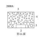
第6A~6F圖顯示本發明實施例中發光裝置之示意圖。粒子3被加入發光裝置2000A、2000B與2000E的波長轉換層4之內、被加入發光裝置2000C與2000F的透明層6之內、也被加入發光裝置2000D的透明蓋8之內。粒子3被用來增進光線的散射或者反射。粒子3不是透明的,並且至少吸收一部分從發光二極體所發出的光線。藉由粒子3的加入,發光裝置2000A~2000F的空間色度均勻性可以獲得改善,但是光萃取效率也分別降低了35%、5%、31%、54%、4%與43%。Figures 6A to 6F show schematic diagrams of the light-emitting device in an embodiment of the present invention. The
如第3A~3E圖所示,光萃取效率並不會受到側壁表面反射率顯著影響,不論側壁的表面是Lambertian散射表面或者是反射率為100%的表面。如第1A~1H、4A~4C、5A~5C與6A~6F圖所示,光萃取效率比較容易受載板10的表面的反射率或者發光裝置的尺寸所影響。例如,載板10的表面的反射率越高,光萃取效率可以提升約18%~20%。或者在發光裝置與載板10之間設置反射層也可以增加約11~12%的光萃取效率。再者,具有類似色度空間均勻度的發光裝置之間,也可以藉由增加發光裝置的尺寸來提升光萃取效率。例如當發光裝置的尺寸是發光二極體的25倍或者更多的時候,光萃取效率可以從127 lm/W增加到138/W,也就是大約增加了8%的光萃取效率。As shown in Figures 3A to 3E, the light extraction efficiency will not be significantly affected by the reflectivity of the sidewall surface, regardless of whether the surface of the sidewall is a Lambertian scattering surface or a surface with a reflectivity of 100%. As shown in Figures 1A to 1H, 4A to 4C, 5A to 5C, and 6A to 6F, the light extraction efficiency is relatively easily affected by the reflectivity of the surface of the
除此之外,HWR或者結構內的粒子3也能影響發光裝置所發出的光線均勻度。例如,當HWR介於1.1~1.3之間的時候各角度上的色度空間均勻性△u’ v’便低於0.04。又例如,當結構內的粒子3的濃度大約是5%的時候,在-80°~+80°之間的色度空間均勻性△u’ v’便低於0.01。In addition, the
第7A~7F圖顯示本發明實施例中發光組件的示意圖與一些相關的光學特性。第7A、7C與7E圖中帶有箭頭的折線代表的是光在發光組件內的路徑,而第7B、7D與7F圖中顯示的是這些發光組件的發光圖案的光場影像。Figures 7A to 7F show schematic diagrams of light-emitting components and some related optical characteristics in an embodiment of the present invention. The broken lines with arrows in Figures 7A, 7C, and 7E represent the path of light in the light-emitting components, and Figures 7B, 7D, and 7F show the light field images of the light-emitting patterns of these light-emitting components.
第7A圖中的發光組件具有一個發光裝置3000形成於一個載板10之上的發光裝置3000、一覆蓋發光裝置3000的第一透鏡160、一位於第一透鏡160之上的第二透鏡162、以及一位於第二透鏡162之上的波長轉換層4。從發光裝置3000所發出來的光線首先被第一透鏡160改變方向後再進入第二透鏡162。從第一透鏡160過來的光線接著被第二透鏡162改變方向並往大體上垂直於載板10的方向前進。如第7B圖所示,發光圖案的內部區域具有較高的亮度,而內部區域大致上對應到第一透鏡160的尺寸與形狀。內部區域與整個光場的面積比例,大致對應到第一透鏡160與第二透鏡162的正向投影面積比。The light-emitting assembly in Figure 7A has a light-emitting
詳言之,如第7A圖所示,透鏡162有一與波長轉換層4相接的上表面、一下表面、複數個側壁與一用以容納著第一透鏡160與發光裝置3000的凹穴。凹穴有一個凸面往發光裝置3000的方向凸起,並有一個大致跟透鏡160相等的寬度。而複數個側壁由上表面往下表面的方向,往內互相靠近。換句話說,從剖面圖/上視圖來看,上表面比下表面大/寬。側壁可以是平面、曲面,或者是平面與曲面的組合。在一實施例中,上表面或者下表面可以是圓形、橢圓形、矩形、三角形,或其它幾何形狀。不僅如此,上表面與下表面可以有相同或者不同的形狀。當發光裝置3000所發出的光線的角度不同的時候,這些光線可以被側壁或者凸面反射或者散射。如圖所示,相較於透鏡162上表面的周圍區域,凸面可以往透鏡162的上表面的中心區域匯集較多的光線(或以使光線以準直方式前進),如第7B圖所示。In detail, as shown in FIG. 7A, the
如第7C圖所示,大部分從發光裝置3000發出的光線被第一透鏡160散射後,被重新導向到第三透鏡164的邊緣或周緣,並且被第三透鏡164反射。所以,如第7D圖所示,發光圖案的邊緣或周緣會比內部區域更亮。As shown in FIG. 7C, most of the light emitted from the
詳言之,如第7C圖所示,透鏡164具有一個與波長轉換層4相連的上表面、一下表面、複數個側壁與一個孔穴以容納透鏡160與發光裝置3000。孔穴的剖面是三角形,其具有傾斜邊緣。孔穴的下方寬度比透鏡160的最大寬度更大。在數個實施例中,相較於透鏡164的上表面的中間區域,傾斜的邊緣(或表面)可以分散更多的光線到透鏡164的上表面的周圍區域,如第7D圖所示。In detail, as shown in FIG. 7C, the
如第7E圖所示,第四透鏡166具有跟第二透鏡162相似的結構。詳言之,如第7E圖所示,透鏡166具有一個平坦的上表面連接到波長轉換層4、一下表面、複數個側面與一孔穴以容納透鏡160與發光裝置3000。孔穴具有一個凸面,這個凸面的曲率比162的孔穴的凸面更小。從發光裝置3000發出的光線會先被透鏡160彎折後再於透鏡166內向外地移動到透鏡166。相較於第7A圖所示的結構,光線被透鏡160(尤其是凸面)所散射,而不是如第7A圖所示,光線以準直的方式以垂直於載板10的方向移動。另外,發光裝置3000發出的光線也會被透鏡166的側壁所反射。第7F圖所顯示的發光圖案相較於第7B圖的光學圖案,在光強度分布上具有更好的均勻度。As shown in FIG. 7E, the
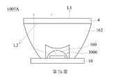
第7G圖所顯示的是發光組件中,從於波長轉換層4發出的正向光線(L1)光線與背向光線(L2)。光線L1與光線L2在不同的發光組件中可以具有不同的光學特性,下表所顯示的的就是第7A、7C、7E圖中的發光組件的光線L1與光線L2的特性差異。例如,在第7A圖的發光組件中,正向光線(L1)與背向光線(L2)之間的色溫差異小於1000K,並且正向光線(L1)與背向光線(L2)之間的光萃取效率差異大於10 lm/W。Figure 7G shows the forward light (L1) light and the back light (L2) emitted from the

第7A圖中的波長轉換層4的螢光粉濃度30%並且厚度為0.5mm,而第7E圖中的波長轉換層4的螢光粉濃度50%並且厚度為0.25mm。第7C圖中的波長轉換層4的厚度為0.45mm,而外側區域的螢光粉濃度為30%,內側區域的螢光粉濃度為10%,如第7H圖所示。在一實施例中,從發光裝置發出的光線與波長轉換層之間的夾角幾乎不會影響從發光組件所發出的光線的光學特性。參考第7I~7J圖,三個入射光線與波長轉換層的夾角分別是45°、60°與90°,如第7I圖所示。而在波長轉換層相對於這三個光線一的另一側,所量測到對應這三個光線的光強度幾乎相同,如第7J圖所示。The
第8A圖所顯示的是發光組件1008A的示意圖。發光組件1008A具有一由一第一波長轉換層40、一第二波長轉換層42以及形成於波長轉換層40與42之間的透明層60所堆疊的疊層。第8A圖中的發光組件1008A所發出的光線,其光學特性會被這疊層的某些特性所影響,例如第一波長轉換層40與第二波長轉換層42的厚度以及第一波長轉換層40與第二波長轉換層42的重量百分濃度(wt%)都是可能會影響發光組件1008A的光萃取效率的參數。光線較容易被具有較高重量百分濃度的波長轉換層吸收,因此光萃取效率在較多的光線被波長轉換層吸收的情況下也降低了。當波長轉換層的厚度越厚時,表示光線在波長轉換層內要經過更長的距離,因此,光線也更容易被吸收而降低光萃取效率。在另一實施例中,參考第8B圖,這個疊層是設計讓光線會在穿過第二波長轉換層42之前,讓光線先在第一波長轉換層40與第二波長轉換層42之間來回反射。在一實施例中,參考下表,第一波長轉換層40的濃度為70%,第二波長轉換層40的濃度為5%,第一波長轉換層40與第二波長轉換層42的厚度都是0.3mm。正向光線(L1)與背向光線(L2)的色溫(CCT)標準差在第7A圖的發光組件1007A中為2720.383,但在第8A圖的發光組件1008A中為1258.146。第7A圖中的發光組件1007A的總光萃取效率(大約是138.256 lm/W)跟第8A圖中的發光組件1008A的總光萃取效率(大約是137.087 lm/W)相近。藉由使用具有兩層波長轉換層的結構,第8A圖中的組件1008A在正向與背向的方向上可以維持相近的光萃取效率並提供較佳的色溫(CCT)標準差。在一實施例中,第一波長轉換層40的螢光粉濃度對正向光(L1)色溫(CCT)的影響,比起第二波長轉換層42的螢光粉濃度對背向光(L2)色溫(CCT)的影響大。Figure 8A shows a schematic diagram of the light-emitting

第8C~8D圖所顯示的是根據本發明之實施例的發光組件。第8C圖中的發光組件1008C具有分別設置在兩個載板10之上的兩個發光裝置3000,可以朝左邊以及右邊發出光線。位於透鏡170a與170b之間的波長轉換層44的左右兩側可以用來吸收並轉換來自兩個發光裝置3000的光線。這兩個光源都發出相同的色光,例如紅外光、紅光、綠光、藍光與紫外光。一實施例中,發光組件1008C的色溫在波長轉換層44內的波長轉換粒子濃度增加時,可以被降低到6500K。然而,當波長轉換層44內的波長轉換材料濃度增加到30%或者更多的時候,色溫將會在6500K左右維持不變。同樣的,波長轉換層44內的波長轉換粒子濃度增加時,發光效率也隨之增加。光萃取效率可以提升到大約290 lm/W。但在波長轉換層44內的波長轉換材料濃度增加到30%或者更多的時候光萃取效率將被維持在290 lm/w左右。Figures 8C to 8D show light-emitting components according to embodiments of the present invention. The light-emitting
第8D圖中的組件1008D具有一發光裝置3000位於載板10之上、兩個波長轉換層46與48,以及一個透鏡172覆蓋著發光裝置3000與這些波長轉換層46與48。參考第8D圖,光線(L1)與光線(L3)被重新導向後入射到波長轉換層46與48的正面的一側,以及光線(L2)與光線(L4)被重新導向後入射到波長轉換層46與48的背面的一側。在一實施例中,波長轉換層46與48的厚度都是0.55mm。The
發光組件的光學特性如下表所列,透鏡172以中心軸或者中心平面(圖未示)相對稱,因此可以提供對稱的光路徑。換句話說,光線L1與L3彼此互為鏡像,光線L2與光線L4也彼此互為鏡像。光線L1與光線L2或者光線L3與光線L4之間的色溫標準差小於600K,也比第7A圖中的光學組件的標準差低。光萃取效率大於150 lm/W,則是比第7A圖中的光學組件的光萃取效率高。The optical characteristics of the light-emitting components are listed in the following table. The


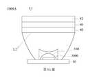
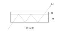
第9A~9D圖顯示根據本發明實施例的多個發光組件的示意圖。參考第9A圖,透鏡174A與波長轉換層50光耦合。光線可以從透鏡的一側進入,再從另一側離開。當光線的入射角度可以適當的控制,並在透鏡174內部的上表面與下表面之間產生全反射的時候,光線便可以在透鏡174內來回反射,而光線可以從不同的位置撞擊波長轉換層50並被吸收。越多光線被吸收,波長轉換層50也就能產生更多被轉換的光線。Figures 9A-9D show schematic diagrams of a plurality of light-emitting components according to an embodiment of the present invention. Referring to FIG. 9A, the lens 174A is optically coupled with the
第9B圖中的發光組件1009B有一個發光裝置4000設置於載板10之上、一具有孔穴1740的透鏡174,以及一設置於透鏡174上的波長轉換層50。發光裝置4000被設置在孔穴1740內,並被透鏡174完全覆蓋。第9C圖顯示的是透鏡174正向側的發光圖,第9D圖顯示的是透鏡174背向側的發光圖。發光組件1009B的光學特性如下所列,其中光線L1與L2的色溫的標準差低於200K,整體的光萃取效率為140 lm/w左右。The light-emitting


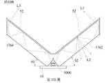
第10A~10D圖顯示根據本發明一實施例的發光組件的示意圖。參考第10A~10B圖,光線在透鏡176內來回反射。透鏡176具有一第一翼部1760與一第二翼部1762。第一翼部1760與載板10之間夾有一傾斜角度θ1。第二翼部1762與載板10之間夾有一傾斜角度θ2。在一實施例中,傾斜角度θ1與傾斜角度θ2同樣都是30°。如第10A圖所示,光線L1在第二翼部1762內反射兩次或者多次後再穿過波長轉換層52,光線L2在第二翼部1762內反射兩次或者多次後再往遠離波長轉換層52的方向移動,並且不會穿過波長轉換層52。波長轉換層52不僅位於第一翼部1760與第二翼部1762之間的表面S1與S2之上,也位於第一翼部1760的邊緣E2以及第二翼部1762的邊緣E1之上。如第10B圖所示,第一翼部1760與第二翼部1762以V形/U形的形狀在發光裝置5000之上分叉,光線L1與L3在圖中以類似的路徑移動著。藉由使用第10A~10B圖中的透鏡,光線L1~L3的波長更容易被波長轉換層52轉換。第10B圖中的發光組件具有一個發光裝置5000位於載板10之上、一具有第一翼部1760與第二翼部1762的透鏡176,以及一個波長轉換層52。第10C圖顯示相對於透鏡176而言的正向側的圖,並且第10D圖中所顯示相對於透鏡176而言的背向側的圖。組件的光學特性如下所列,光線L1與L2的色溫標準差低於700K,而總光萃取效率則大於150 lm/W。Figures 10A to 10D show schematic diagrams of a light-emitting component according to an embodiment of the invention. Referring to FIGS. 10A to 10B, the light is reflected back and forth in the

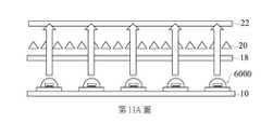
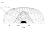
參考第11A圖,組件具有多個發光裝置6000(圖中顯示五個發光裝置6000,但是發光裝置的數量可多可少)、一個與發光裝置6000之間存在一距離的擴散層18、一個位於擴散層18之上的稜鏡層20,以及一位於稜鏡層20之上的液晶螢幕(LCD)模組22,發光裝置6000、擴散層18與稜鏡層20可以組成一個液晶顯示器的背光模組,液晶螢幕(LCD)模組22具有一個透鏡。擴散層18可以重新分配來自發光裝置6000的光線,以增加發光裝置6000的光均勻度,而稜鏡層20具有多個稜鏡以集中光線。因此,LCD模組22上的光場均勻度也增加了。在一實施例中,液晶螢幕(LCD)模組22內的透鏡跟發光裝置6000之間的距離大於兩個相鄰發光裝置的距離。Referring to Figure 11A, the assembly has multiple light-emitting devices 6000 (five light-emitting
第11B圖顯示的是組件的示意圖。標號H代表發光裝置6000與LCD模組22之間的距離,標號R代表的是發光區域在LCD模組22上的半徑,而標號d代表相鄰發光裝置間的側向的距離。H越小也代表LCD模組22上的光場越小,也就是半徑R越小。在一實施例中,發光裝置6000在液晶螢幕(LCD)模組22(或者是模組內的透鏡)上的光場半徑大小等於兩個發光裝置6000之間距離的兩倍。第11C~11D圖顯示的是發光裝置6000的排列的上視圖示意圖。發光裝置6000在第11C圖中被排列成彼此相連的三角形,而發光裝置6000在第11D圖中被排列成彼此相連的四方形。發光裝置被排列成不同的形狀,可以提供不同的光學分布。第11C圖中的排列的單位面積所提供的照度分布圖如第11E圖所示,第11D圖中的排列的單位面積所提供的照度分布圖如第11E圖所示。在一實施例中,單一個發光裝置6000的光場的半徑R可以被設定成與相鄰發光裝置6000之間的最短距離相同。如第11E與11F圖所示,不同的顏色各自代表不同的照明程度,而顏色與照明程度的詳細對照可以參照圖中的圖例。Figure 11B shows a schematic diagram of the components. The symbol H represents the distance between the light-emitting
在本實施例中,第11G圖是一個發光裝置6000在X方向上的位移所造成光學均勻度的變化的示意圖,第11H圖一個發光裝置6000在Y方向上的位移所造成光學均勻度的變化的示意圖。第11G或者第11H圖中的橫座標代表的是發光組件內的一個發光裝置6000的位置相對於原本位置的偏移距離,第11G或者第11H圖中的縱座標代表的是發光組件歸一化的照度均勻度。如第11G與第11H圖所示,正向(X>0或者Y>0)與負向(X<0或者Y<0)的位移在四方形的排列方式中,都對照度的均勻度造成類似的降低幅度。然而在三角形排列方式,正向(X>0或者Y>0)與負向(X<0或者Y<0)的位移對照度的均勻度的影響則不同。對三角形的排列方式而言,負向的位移所造成的照度均勻度的減少,比正向的位移所造成的減少更多。不論是在三角形排列或者四方形排列,發光裝置所在的位子於X方向或者Y方向上(往正向或者往負向)有0.1mm的位移時,光學均勻度都會降到低於最大值的0.9倍。In this embodiment, Fig. 11G is a schematic diagram of the change in optical uniformity caused by the displacement of the light-emitting
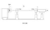
第12A~12B圖所顯示的是根據本發明一實施例的量測設備。第12A圖中的設備可以量測發光裝置7000所發出光線的遠場光學特性,從發光裝置7000發出的光線可經過第一光圈178a與第二光圈178b後被光譜儀24接收。第一光圈178a與第二光圈178b移除部分光線,並保留在特定角度的光線讓光譜儀24吸收。第12B圖的設備可以量測發光裝置7000所發出光線的中場光學特性,而從發光裝置7000發出的光線可經過凸透鏡180後,被光譜儀24接收。Figures 12A to 12B show a measurement device according to an embodiment of the present invention. The device in Figure 12A can measure the far-field optical characteristics of the light emitted by the
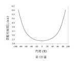
第12C~12E圖顯示的是部分利用第12A圖中的裝置所得到的量測結果,其中12C~12E圖的0度大致對應到發光裝置7000的中心,而角度代表著量測點與發光裝置7000中心的夾角。第12C圖則分別顯示了歸一化後藍光的光強度、黃光的光強度,以及整體的光強度。全部的光線可以有藍光、黃光或者其他色光。如圖中所示,不同光線在不同的角度上有不同的強度。第12D圖則分別顯示了黃光的光強度與藍光的光強度的比值YBR,這個比值隨著角度的絕對值增加而增加。尤其是黃光在較大的角度上更容易被觀察到,而這也造成發光圖案在圖案的周圍有一個偏黃的區域。參考第12E圖,相關色溫CCT由0度大於6500K(發光裝置中心附近)降低到90度時大約4500K(發光裝置周圍附近)。Figures 12C~12E show the measurement results obtained partially using the device in Figure 12A, where 0 degree in Figure 12C~12E roughly corresponds to the center of the light-emitting
如第13圖所示,透鏡184可以裝置到發光裝置8000以均勻化所發出的光線的照度與顏色。透鏡184可以將藍光轉往到更大角度的方向,以及將黃光轉向較小角度的方向。透鏡184具有一個主體與一個位於主體下表面的孔穴1840,孔穴1840界定了一個空間以容納發光裝置8000。孔穴1840的剖面圖有一個上內表面以及一個下內表面。上內表面具有一個鐘形/拱形的形狀/輪廓。下內表面具有一個延伸到透鏡184下表面的拖尾。上內表面與下內表面可以有相同或者不同的曲率。此外,上內表面自身或者下內表面自身可以有一個或者多個曲率。透鏡184的外表面有數個相連接的區域(如第13圖所示,這些區域在剖面圖上可以視為線段),相鄰區域的連接部分可以有著可察覺到的角度變化以將特定的色光導引至特定的方向。舉例來說,具有較短波長的色光,例如藍光,撞到較高區域的時候可以被向下彎折;而具有較長波長的色光,例如黃光,撞到較低區域的時候可以被向上彎折。As shown in FIG. 13, the
本發明同時主張美國暫時申請案第62/029977號與美國正式申請案第14/810180號的優先權,其中美國暫時申請案第62/029977號所包含的中文論文及相關檔案皆援引為本申請案之一部分。The present invention also claims the priority of U.S. Provisional Application No. 62/029977 and U.S. Formal Application No. 14/810180. The Chinese papers and related files contained in U.S. Provisional Application No. 62/029977 are all cited as this application. Part of the case.
需了解的是,本發明中上述之實施例在適當的情況下,是可互相組合或替換,而非僅限於所描述之特定實施例。本發明所列舉之各實施例僅用以說明本發明,並非用以限制本發明之範圍。任何人對本發明所作之任何顯而易見之修飾或變更接不脫離本發明之精神與範圍。It should be understood that the above-mentioned embodiments of the present invention can be combined or replaced with each other under appropriate circumstances, and are not limited to the specific embodiments described. The embodiments listed in the present invention are only used to illustrate the present invention, and are not used to limit the scope of the present invention. Any obvious modification or alteration of the present invention by anyone does not depart from the spirit and scope of the present invention.
4‧‧‧波長轉換層4‧‧‧Wavelength conversion layer
10‧‧‧載板10‧‧‧Carrier Board
160、162‧‧‧透鏡160、162‧‧‧lens
L1、L2‧‧‧光線L1, L2‧‧‧Light
3000‧‧‧發光裝置3000‧‧‧Lighting Device
1007A‧‧‧發光組件1007A‧‧‧Light-emitting components
Claims (5)
Translated fromChineseApplications Claiming Priority (4)
| Application Number | Priority Date | Filing Date | Title |
|---|---|---|---|
| US201462029977P | 2014-07-28 | 2014-07-28 | |
| US62/029977 | 2014-07-28 | ||
| US14/810180 | 2015-07-27 | ||
| US14/810,180US9911907B2 (en) | 2014-07-28 | 2015-07-27 | Light-emitting apparatus |
Publications (2)
| Publication Number | Publication Date |
|---|---|
| TW201929270A TW201929270A (en) | 2019-07-16 |
| TWI728348Btrue TWI728348B (en) | 2021-05-21 |
Family
ID=55349017
Family Applications (2)
| Application Number | Title | Priority Date | Filing Date |
|---|---|---|---|
| TW104124413ATWI661581B (en) | 2014-07-28 | 2015-07-28 | Light-emitting apparatus |
| TW108113852ATWI728348B (en) | 2014-07-28 | 2015-07-28 | Light-emitting apparatus |
Family Applications Before (1)
| Application Number | Title | Priority Date | Filing Date |
|---|---|---|---|
| TW104124413ATWI661581B (en) | 2014-07-28 | 2015-07-28 | Light-emitting apparatus |
Country Status (2)
| Country | Link |
|---|---|
| US (3) | US9911907B2 (en) |
| TW (2) | TWI661581B (en) |
Families Citing this family (7)
| Publication number | Priority date | Publication date | Assignee | Title |
|---|---|---|---|---|
| JP6339053B2 (en)* | 2014-09-30 | 2018-06-06 | 富士フイルム株式会社 | Wavelength conversion member, backlight unit including the same, and liquid crystal display device |
| US20180323354A1 (en)* | 2017-05-07 | 2018-11-08 | Yang Wang | Light emitting device and method for manufacturing light emitting device |
| CN112955805B (en)* | 2018-10-04 | 2023-08-01 | 幹太向·牛方株式会社 | Optical system device and lenticular lens |
| CN214375712U (en) | 2020-06-30 | 2021-10-08 | 光森科技有限公司 | Light source module |
| TWM607954U (en)* | 2020-06-30 | 2021-02-21 | 光森科技有限公司 | Light source module |
| TWI801848B (en) | 2021-04-23 | 2023-05-11 | 元太科技工業股份有限公司 | Reflective display and white light source thereof |
| WO2023112426A1 (en)* | 2021-12-15 | 2023-06-22 | 株式会社ジャパンディスプレイ | Display device |
Citations (6)
| Publication number | Priority date | Publication date | Assignee | Title |
|---|---|---|---|---|
| US20110292302A1 (en)* | 2010-04-30 | 2011-12-01 | Samsung Led Co., Ltd. | Light emitting device package, light source module, backlight unit, display apparatus, television set, and illumination apparatus |
| TW201218450A (en)* | 2010-10-22 | 2012-05-01 | Advanced Optoelectronic Tech | Encapsulation, light-emitting diode package and method for manufacturing encapsulation |
| US20120132944A1 (en)* | 2010-11-29 | 2012-05-31 | Epistar Corporation | Light-emitting device, light mixing device and manufacturing methods thereof |
| TWM449358U (en)* | 2012-11-14 | 2013-03-21 | Camaro Internat Co Ltd | Light-emitting diode packaging structure |
| US20130187178A1 (en)* | 2012-01-24 | 2013-07-25 | Michael A. Tischler | Light-emitting dies incorporating wavelength-conversion materials and related methods |
| US8686625B1 (en)* | 2013-03-14 | 2014-04-01 | Cooledge Lighting Inc. | Engineered-phosphor LED packages and related methods |
Family Cites Families (41)
| Publication number | Priority date | Publication date | Assignee | Title |
|---|---|---|---|---|
| AU2002359708A1 (en)* | 2001-12-14 | 2003-07-15 | Digital Optics International Corporation | Uniform illumination system |
| WO2003077389A1 (en)* | 2002-03-08 | 2003-09-18 | Sharp Kabushiki Kaisha | Light source apparatus and optical communication module comprising it |
| KR20040074789A (en)* | 2003-02-19 | 2004-08-26 | 삼성전자주식회사 | Backlight assembly and liquid crystal display having the same |
| US7121690B1 (en)* | 2004-02-26 | 2006-10-17 | Advanced Optical Technologies, Llc | Constructive occlusion with a transmissive component |
| TWI241038B (en)* | 2004-09-14 | 2005-10-01 | Ind Tech Res Inst | Light emitting diode structure and fabrication method thereof |
| KR100616625B1 (en)* | 2004-10-20 | 2006-08-28 | 삼성전기주식회사 | Large screen backlight unit with reduced thickness |
| CN101086577A (en) | 2006-06-07 | 2007-12-12 | 中国科学院半导体研究所 | LCD backlight source structure of LED illumination |
| US7804147B2 (en)* | 2006-07-31 | 2010-09-28 | Cree, Inc. | Light emitting diode package element with internal meniscus for bubble free lens placement |
| US20080029775A1 (en)* | 2006-08-02 | 2008-02-07 | Lustrous Technology Ltd. | Light emitting diode package with positioning groove |
| KR100828900B1 (en)* | 2006-09-04 | 2008-05-09 | 엘지이노텍 주식회사 | Light emitting diode package and manufacturing method thereof |
| KR20080038878A (en)* | 2006-10-31 | 2008-05-07 | 삼성전자주식회사 | Light source device and liquid crystal display device including the same |
| GB2447443A (en)* | 2007-03-05 | 2008-09-17 | Sharp Kk | Backlight and display |
| US7687816B2 (en)* | 2007-03-20 | 2010-03-30 | International Business Machines Corporation | Light emitting diode |
| KR101289069B1 (en)* | 2007-05-09 | 2013-07-22 | 엘지디스플레이 주식회사 | Light emitting diode package having structure of dual lens and liquid crystal display device thereby |
| US7942556B2 (en)* | 2007-06-18 | 2011-05-17 | Xicato, Inc. | Solid state illumination device |
| TW200936953A (en) | 2008-02-29 | 2009-09-01 | Univ Nat Chiao Tung | Structure of LED lens with reflective film |
| CN101651177B (en) | 2008-08-11 | 2012-06-13 | 旭丽电子(广州)有限公司 | Photoelectric semiconductor device capable of generating uniform polychromatic light |
| US8129735B2 (en)* | 2008-09-24 | 2012-03-06 | Koninklijke Philips Electronics N.V. | LED with controlled angular non-uniformity |
| US7897419B2 (en)* | 2008-12-23 | 2011-03-01 | Cree, Inc. | Color correction for wafer level white LEDs |
| WO2011025724A1 (en)* | 2009-08-27 | 2011-03-03 | Dolby Laboratories Licensing Corporation | Optical mixing and shaping system for display backlights and displays incorporating the same |
| JP5047264B2 (en)* | 2009-12-22 | 2012-10-10 | 株式会社東芝 | Light emitting device |
| CN102142501A (en) | 2010-01-28 | 2011-08-03 | 海洋王照明科技股份有限公司 | LED encapsulation structure |
| JP5340191B2 (en)* | 2010-02-02 | 2013-11-13 | 日東電工株式会社 | Optical semiconductor device |
| CN101782203B (en) | 2010-02-04 | 2012-02-01 | 广东昭信光电科技有限公司 | Backlight system containing free-form surface reflector |
| JP5678629B2 (en)* | 2010-02-09 | 2015-03-04 | ソニー株式会社 | Method for manufacturing light emitting device |
| US9062830B2 (en)* | 2010-03-03 | 2015-06-23 | Cree, Inc. | High efficiency solid state lamp and bulb |
| US20120051047A1 (en)* | 2010-08-30 | 2012-03-01 | Edison Opto Corporation | Street lamp |
| CN102588816B (en) | 2011-01-07 | 2017-12-01 | 晶元光电股份有限公司 | Light emitting device, light mixing device, and method for manufacturing light emitting device |
| CN102654273B (en) | 2011-03-04 | 2014-05-28 | 海洋王照明科技股份有限公司 | Condenser lens of LED (light emitting diode) |
| CN102748709B (en) | 2011-04-21 | 2014-05-14 | 海洋王照明科技股份有限公司 | Full-reflection lens and LED (Light-Emitting Diode) lamp using same |
| US8757845B2 (en)* | 2011-07-29 | 2014-06-24 | TSMC Solid State Lighting, Ltd. | Wide angle based indoor lighting lamp |
| CN102306698A (en) | 2011-09-30 | 2012-01-04 | 深圳市灏天光电有限公司 | Novel LED packaging structure |
| FR2981506B1 (en)* | 2011-10-18 | 2014-06-27 | Commissariat Energie Atomique | ELECTROLUMINESCENT DIODE COMPONENT |
| US8564004B2 (en)* | 2011-11-29 | 2013-10-22 | Cree, Inc. | Complex primary optics with intermediate elements |
| US9065024B2 (en)* | 2012-05-01 | 2015-06-23 | Bridgelux, Inc. | LED lens design with more uniform color-over-angle emission |
| US8629466B2 (en) | 2012-05-22 | 2014-01-14 | Hong Kong Applied Science and Technology Research Institute Company Limited | Lighting device |
| US9166116B2 (en) | 2012-05-29 | 2015-10-20 | Formosa Epitaxy Incorporation | Light emitting device |
| TWI564854B (en)* | 2012-11-14 | 2017-01-01 | 晶元光電股份有限公司 | Light-emitting device and driving method for light-emitting diode |
| EP3005427B1 (en) | 2013-06-06 | 2019-01-16 | Lumileds Holding B.V. | Manufacturing method of light emitting diode laminated with a phosphor sheet |
| CN203521459U (en) | 2013-09-24 | 2014-04-02 | 璨圆光电股份有限公司 | Light emitting module and light emitting device |
| TWM475702U (en)* | 2013-12-11 | 2014-04-01 | Genesis Photonics Inc | Light emitting diode package structure |
- 2015
- 2015-07-27USUS14/810,180patent/US9911907B2/enactiveActive
- 2015-07-28TWTW104124413Apatent/TWI661581B/enactive
- 2015-07-28TWTW108113852Apatent/TWI728348B/enactive
- 2018
- 2018-03-06USUS15/913,865patent/US20180198039A1/ennot_activeAbandoned
- 2020
- 2020-06-08USUS16/895,807patent/US11165000B2/enactiveActive
Patent Citations (6)
| Publication number | Priority date | Publication date | Assignee | Title |
|---|---|---|---|---|
| US20110292302A1 (en)* | 2010-04-30 | 2011-12-01 | Samsung Led Co., Ltd. | Light emitting device package, light source module, backlight unit, display apparatus, television set, and illumination apparatus |
| TW201218450A (en)* | 2010-10-22 | 2012-05-01 | Advanced Optoelectronic Tech | Encapsulation, light-emitting diode package and method for manufacturing encapsulation |
| US20120132944A1 (en)* | 2010-11-29 | 2012-05-31 | Epistar Corporation | Light-emitting device, light mixing device and manufacturing methods thereof |
| US20130187178A1 (en)* | 2012-01-24 | 2013-07-25 | Michael A. Tischler | Light-emitting dies incorporating wavelength-conversion materials and related methods |
| TWM449358U (en)* | 2012-11-14 | 2013-03-21 | Camaro Internat Co Ltd | Light-emitting diode packaging structure |
| US8686625B1 (en)* | 2013-03-14 | 2014-04-01 | Cooledge Lighting Inc. | Engineered-phosphor LED packages and related methods |
Also Published As
| Publication number | Publication date |
|---|---|
| US20160056348A1 (en) | 2016-02-25 |
| US20200303601A1 (en) | 2020-09-24 |
| TW201929270A (en) | 2019-07-16 |
| US11165000B2 (en) | 2021-11-02 |
| US20180198039A1 (en) | 2018-07-12 |
| TWI661581B (en) | 2019-06-01 |
| US9911907B2 (en) | 2018-03-06 |
| TW201605074A (en) | 2016-02-01 |
Similar Documents
| Publication | Publication Date | Title |
|---|---|---|
| TWI728348B (en) | Light-emitting apparatus | |
| US20240044476A1 (en) | Light source device and display unit | |
| JP5279329B2 (en) | Light-emitting unit with lens | |
| CN106684108B (en) | Light emitting diode display device | |
| US7370993B2 (en) | Light recycling illumination systems having restricted angular output | |
| CN102798002B (en) | Light source device with external lens and light source system | |
| JP5917723B2 (en) | Surface light source | |
| US20090046459A1 (en) | Lighting device | |
| CN105318278B (en) | light emitting assembly | |
| US8801221B2 (en) | Lens structure, light source device and light source module | |
| TWM580691U (en) | A direct type backlight device | |
| US10564470B2 (en) | Backlighting device | |
| CN103988017A (en) | indirect lighting | |
| KR102304267B1 (en) | Light emitting device package and backlight unit including the package | |
| JP6196018B2 (en) | Light emitting device | |
| JP6812185B2 (en) | Organic EL display device | |
| TWI579504B (en) | Light emitting device | |
| JP7164600B2 (en) | lighting equipment |