TWI728275B - Organic light-emitting diode touch display operating method - Google Patents
Organic light-emitting diode touch display operating methodDownload PDFInfo
- Publication number
- TWI728275B TWI728275BTW107139054ATW107139054ATWI728275BTW I728275 BTWI728275 BTW I728275BTW 107139054 ATW107139054 ATW 107139054ATW 107139054 ATW107139054 ATW 107139054ATW I728275 BTWI728275 BTW I728275B
- Authority
- TW
- Taiwan
- Prior art keywords
- time
- touch
- display
- emitting diode
- organic light
- Prior art date
Links
Images


Classifications
- G—PHYSICS
- G06—COMPUTING OR CALCULATING; COUNTING
- G06F—ELECTRIC DIGITAL DATA PROCESSING
- G06F3/00—Input arrangements for transferring data to be processed into a form capable of being handled by the computer; Output arrangements for transferring data from processing unit to output unit, e.g. interface arrangements
- G06F3/01—Input arrangements or combined input and output arrangements for interaction between user and computer
- G06F3/03—Arrangements for converting the position or the displacement of a member into a coded form
- G06F3/041—Digitisers, e.g. for touch screens or touch pads, characterised by the transducing means
- G06F3/0416—Control or interface arrangements specially adapted for digitisers
- G06F3/0418—Control or interface arrangements specially adapted for digitisers for error correction or compensation, e.g. based on parallax, calibration or alignment
- G06F3/04184—Synchronisation with the driving of the display or the backlighting unit to avoid interferences generated internally
- H—ELECTRICITY
- H10—SEMICONDUCTOR DEVICES; ELECTRIC SOLID-STATE DEVICES NOT OTHERWISE PROVIDED FOR
- H10K—ORGANIC ELECTRIC SOLID-STATE DEVICES
- H10K59/00—Integrated devices, or assemblies of multiple devices, comprising at least one organic light-emitting element covered by group H10K50/00
- H10K59/40—OLEDs integrated with touch screens
- G—PHYSICS
- G06—COMPUTING OR CALCULATING; COUNTING
- G06F—ELECTRIC DIGITAL DATA PROCESSING
- G06F3/00—Input arrangements for transferring data to be processed into a form capable of being handled by the computer; Output arrangements for transferring data from processing unit to output unit, e.g. interface arrangements
- G06F3/01—Input arrangements or combined input and output arrangements for interaction between user and computer
- G06F3/03—Arrangements for converting the position or the displacement of a member into a coded form
- G06F3/041—Digitisers, e.g. for touch screens or touch pads, characterised by the transducing means
- G06F3/0412—Digitisers structurally integrated in a display
Landscapes
- Engineering & Computer Science (AREA)
- General Engineering & Computer Science (AREA)
- Theoretical Computer Science (AREA)
- Human Computer Interaction (AREA)
- Physics & Mathematics (AREA)
- General Physics & Mathematics (AREA)
- Electroluminescent Light Sources (AREA)
- Control Of Indicators Other Than Cathode Ray Tubes (AREA)
- Control Of El Displays (AREA)
Abstract
Description
Translated fromChinese本發明係與顯示裝置有關,尤其是關於一種有機發光二極體觸控顯示裝置運作方法。The invention relates to a display device, and more particularly to an operation method of an organic light-emitting diode touch display device.
請參照圖1,圖1繪示傳統的內嵌式有機發光二極體觸控顯示裝置的疊層結構的示意圖。Please refer to FIG. 1. FIG. 1 is a schematic diagram of a laminated structure of a conventional in-cell organic light emitting diode touch display device.
如圖1所示,基於製程良率及厚度之考量,觸控電極ITO與陰極CA之距離相當接近(<2um),造成觸控電極ITO與陰極CA之間的相互影響相當大。As shown in FIG. 1, based on the consideration of process yield and thickness, the distance between the touch electrode ITO and the cathode CA is quite close (<2um), resulting in a considerable mutual influence between the touch electrode ITO and the cathode CA.
當傳統的內嵌式有機發光二極體觸控顯示裝置的觸控模式與顯示模式同時運作時,有機發光二極體OLED的顯示品質會受到觸控電極ITO進行觸控感測之影響而在顯示畫面中出現色帶(Color Band)及閃爍(Flicker)的現象。When the touch mode and display mode of the traditional in-cell organic light-emitting diode touch display device operate at the same time, the display quality of the organic light-emitting diode OLED will be affected by the touch sensing of the touch electrode ITO. Color band and flicker appear in the display screen.
當傳統的內嵌式有機發光二極體觸控顯示裝置的觸控模式與顯示模式於不同時間運作時,雖可避免觸控與顯示相互干擾,但卻也導致觸控掃描時間受限且間隔需拉長以及觸控功耗增加等問題。When the touch mode and the display mode of the traditional in-cell organic light-emitting diode touch display device operate at different times, although the mutual interference between touch and display can be avoided, it also leads to limited touch scan time and interval Need to stretch and increase touch power consumption and other issues.
有鑑於此,本發明提出一種有機發光二極體觸控顯示裝置運作方法,以有效解決先前技術所遭遇到之上述種種問題。In view of this, the present invention proposes an organic light-emitting diode touch display device operation method to effectively solve the above-mentioned problems encountered in the prior art.
根據本發明之一具體實施例為一種有機發光二極體觸控顯示裝置運作方法。於此實施例中,有機發光二極體觸控顯示裝置運作方法包含下列步驟:控制觸控掃描轉換時序與顯示多工器轉換時序維持特定等距關係;以及當有機發光二極體觸控顯示裝置進行顯示時,有機發光二極體觸控顯示裝置僅於部分的顯示時間進行觸控掃描。A specific embodiment according to the present invention is an operating method of an organic light-emitting diode touch display device. In this embodiment, the operating method of the organic light emitting diode touch display device includes the following steps: controlling the touch scan conversion timing and the display multiplexer conversion timing to maintain a specific equidistant relationship; and when the organic light emitting diode touch display When the device is displaying, the organic light-emitting diode touch display device only performs touch scanning during a part of the display time.
於一實施例中,有機發光二極體觸控顯示裝置於另一部分的顯示時間停止觸控掃描。In one embodiment, the organic light emitting diode touch display device stops the touch scan during another part of the display time.
於一實施例中,有機發光二極體觸控顯示裝置於另一部分的顯示時間進行觸控電壓補償掃描。In one embodiment, the organic light emitting diode touch display device performs touch voltage compensation scanning during another part of the display time.
於一實施例中,當遇到外部的雜訊干擾時,有機發光二極體觸控顯示裝置僅於顯示時間之外的顯示空白區間進行觸控掃描。In one embodiment, when encountering external noise interference, the organic light-emitting diode touch display device only performs touch scanning in the display blank interval outside the display time.
於一實施例中,有機發光二極體觸控顯示裝置還進一步調整觸控掃描頻率,以避開外部雜訊之干擾。In one embodiment, the organic light emitting diode touch display device further adjusts the touch scan frequency to avoid interference from external noise.
於一實施例中,有機發光二極體觸控顯示裝置包含自動切換電路,用以於觸控振盪器與顯示振盪器之間自動切換,以於第一運作模式下提供觸控驅動時脈訊號作為輸出時脈訊號及 於第二運作模式下提供顯示驅動時脈訊號作為輸出時脈訊號。In one embodiment, the organic light-emitting diode touch display device includes an automatic switching circuit for automatically switching between the touch oscillator and the display oscillator to provide a touch drive clock signal in the first operation mode As an output clock signal and provide a display drive clock signal as an output clock signal in the second operation mode.
於一實施例中,自動切換電路包含觸控振盪器、顯示振盪器、多工器及抗尖峰脈衝器。觸控振盪器及顯示振盪器均耦接至多工器。多工器耦接至抗尖峰脈衝器。In one embodiment, the automatic switching circuit includes a touch oscillator, a display oscillator, a multiplexer, and an anti-spike pulser. Both the touch oscillator and the display oscillator are coupled to the multiplexer. The multiplexer is coupled to the anti-spike pulser.
於一實施例中,在第一運作模式下,多工器會自動切換至觸控振盪器並將觸控振盪器所提供的觸控驅動時脈訊號輸出至抗尖峰脈衝器進行處理後提供為輸出時脈訊號。In one embodiment, in the first operating mode, the multiplexer will automatically switch to the touch oscillator and output the touch drive clock signal provided by the touch oscillator to the anti-spike device for processing and then provide it as Output clock signal.
於一實施例中,在第二運作模式下,多工器會自動切換至顯示振盪器並將顯示振盪器所提供的顯示驅動時脈訊號輸出至抗尖峰脈衝器進行處理後提供為輸出時脈訊號。In one embodiment, in the second operation mode, the multiplexer will automatically switch to the display oscillator and output the display driving clock signal provided by the display oscillator to the anti-spike pulser for processing and then provide it as the output clock Signal.
於一實施例中,第一運作模式為顯示休眠模式且第二運作模式為顯示模式/閒置模式。In one embodiment, the first operation mode is a display sleep mode and the second operation mode is a display mode/idle mode.
相較於先前技術,本發明之有機發光二極體觸控顯示裝置運作方法藉由將觸控掃描轉換時序(Touch scan transition timing)與顯示多工器轉換時序(Display multiplexer transition timing)維持特定等距關係的方式讓觸控模式與顯示模式能夠同時運作,但不會在顯示畫面中出現色帶(Color Band)及閃爍(Flicker)的現象,藉以有效改善有機發光二極體觸控顯示裝置的顯示品質,同時亦可避免觸控掃描時間受限且間隔需拉長以及觸控功耗增加等問題,使得觸控訊雜比獲得提升並可提供更多的充電時間。Compared with the prior art, the operating method of the organic light emitting diode touch display device of the present invention maintains specific touch scan transition timing and display multiplexer transition timing. The distance relationship allows the touch mode and the display mode to operate at the same time, but no color band and flicker phenomenon appear in the display screen, so as to effectively improve the organic light-emitting diode touch display device The display quality can also avoid problems such as limited touch scan time, longer intervals, and increased touch power consumption, which improves the touch-to-noise ratio and provides more charging time.
關於本發明之優點與精神可以藉由以下的發明詳述 及所附圖式得到進一步的瞭解。The advantages and spirit of the present invention can be further understood from the following detailed description of the invention and the accompanying drawings.
ITO‧‧‧觸控電極ITO‧‧‧Touch electrode
CA‧‧‧陰極CA‧‧‧Cathode
AD‧‧‧陽極AD‧‧‧Anode
OLED‧‧‧有機發光二極體OLED‧‧‧Organic Light Emitting Diode
SUB‧‧‧基板SUB‧‧‧Substrate
INS‧‧‧絕緣層INS‧‧‧Insulation layer
PLA‧‧‧平坦化層PLA‧‧‧Planarization layer
PAS‧‧‧鈍化層PAS‧‧‧Passivation layer
t1~t6‧‧‧時間t1~t6‧‧‧Time
TCH‧‧‧觸控掃描轉換時序TCH‧‧‧Touch scan conversion timing
TE‧‧‧時脈信號TE‧‧‧clock signal
MUX1~MUX6‧‧‧顯示多工器轉換時序MUX1~MUX6‧‧‧Display multiplexer conversion timing
3‧‧‧自動切換電路3‧‧‧Automatic switching circuit
31‧‧‧觸控振盪器31‧‧‧Touch Oscillator
32‧‧‧顯示振盪器32‧‧‧Display oscillator
33‧‧‧多工器33‧‧‧Multiplexer
34‧‧‧抗尖峰脈衝器34‧‧‧Anti-spike pulser
S1‧‧‧觸控驅動時脈訊號S1‧‧‧Touch drive clock signal
S2‧‧‧顯示驅動時脈訊號S2‧‧‧Display drive clock signal
S3‧‧‧輸出時脈訊號S3‧‧‧Output clock signal
MODE1‧‧‧第一運作模式MODE1‧‧‧First operating mode
MODE2‧‧‧第二運作模式MODE2‧‧‧Second operation mode
MODE3‧‧‧第三運作模式MODE3‧‧‧The third operating mode
Vsync‧‧‧垂直同步訊號Vsync‧‧‧Vertical sync signal
20、400‧‧‧顯示線數量20, 400‧‧‧Display line quantity
S10~S14‧‧‧步驟S10~S14‧‧‧Step
圖1繪示傳統的內嵌式有機發光二極體觸控顯示裝置的疊層結構的示意圖。FIG. 1 is a schematic diagram of the laminated structure of a conventional in-cell organic light emitting diode touch display device.
圖2繪示本發明之觸控掃描轉換時序(Touch scan transition timing)與顯示多工器轉換時序(Display multiplexer transition timing)維持一定等距關係的示意圖。FIG. 2 is a schematic diagram showing that the touch scan transition timing and the display multiplexer transition timing of the present invention maintain a certain equidistant relationship.
圖3繪示觸控驅動時脈訊號與顯示驅動時脈訊號於不同運作模式下自動切換的示意圖。FIG. 3 shows a schematic diagram of the touch driving clock signal and the display driving clock signal automatically switching under different operation modes.
圖4繪示自動切換後之輸出時脈訊號於不同運作模式下與觸控驅動時脈訊號及顯示驅動時脈訊號的對應關係。FIG. 4 shows the corresponding relationship between the output clock signal after automatic switching and the touch driving clock signal and the display driving clock signal in different operation modes.
圖5至圖8B分別繪示透過交錯式的觸控掃描以避免顯示不均勻的不同實施例。5 to 8B respectively show different embodiments of avoiding display unevenness through interlaced touch scanning.
圖9繪示在部分的顯示時間進行觸控掃描(Touch scan)且在另一部分的顯示時間進行觸控電壓補償掃描(Touch voltage compensation scan)的示意圖。FIG. 9 shows a schematic diagram of performing a touch scan during a part of the display time and performing a touch voltage compensation scan during another part of the display time.
圖10至圖13分別繪示透過在不同顯示時間分別進行觸控掃描及觸控電壓補償掃描以避免顯示不均勻的不同實施例。FIGS. 10 to 13 respectively show different embodiments in which touch scanning and touch voltage compensation scanning are performed at different display times to avoid uneven display.
圖14A及圖14B繪示在遇到外部雜訊干擾時動態調整觸控掃描頻率之一實施例。14A and 14B show an embodiment of dynamically adjusting the touch scan frequency when encountering external noise interference.
圖15A及圖15B繪示在遇到外部雜訊干擾時動態調整觸控掃描頻率之另一實施例。15A and 15B show another embodiment of dynamically adjusting the touch scan frequency when encountering external noise interference.
圖16繪示根據本發明之一具體實施例之有機發光二極體觸控顯示裝置運作方法的流程圖。FIG. 16 shows a flowchart of an operation method of an organic light-emitting diode touch display device according to an embodiment of the present invention.
根據本發明之一具體實施例為一種有機發光二極體觸控顯示裝置運作方法,用以運作有機發光二極體觸控顯示裝置,使其觸控模式與顯示模式能夠同時運作,但又不會在顯示畫面中出現色帶(Color Band)及閃爍(Flicker)的現象。實際上,有機發光二極體觸控顯示裝置可以是內嵌式(In-cell)有機發光二極體觸控顯示裝置,但不以此為限。According to a specific embodiment of the present invention, an organic light-emitting diode touch display device operation method is used to operate the organic light-emitting diode touch display device so that the touch mode and the display mode can operate at the same time, but not Color band and flicker will appear in the display screen. In fact, the organic light emitting diode touch display device may be an in-cell organic light emitting diode touch display device, but it is not limited to this.
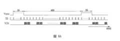
請參照圖2,圖2繪示本發明之觸控掃描轉換時序(Touch scan transition timing)與顯示多工器轉換時序(Display multiplexer transition timing)維持特定等距關係的示意圖。Please refer to FIG. 2. FIG. 2 illustrates a schematic diagram of the touch scan transition timing and the display multiplexer transition timing maintaining a specific equidistant relationship of the present invention.
如圖2所示,當有機發光二極體觸控顯示裝置進行顯示時,可透過共用顯示驅動時脈訊號及顯示驅動器提供時脈信號TE之方式,達到完全控制觸控掃描轉換時序TCH與顯示多工器轉換時序MUX1~MUX6維持特定等距關係而不會互相干擾,藉以避免在顯示畫面中出現色帶(Color Band)及閃爍(Flicker)的現象,並可同時提升觸控感測之訊雜比。As shown in Figure 2, when the organic light-emitting diode touch display device performs display, the display driving clock signal and the display driver can provide the clock signal TE by sharing the display driving clock signal to achieve full control of the touch scan conversion timing TCH and display The multiplexer conversion timing MUX1~MUX6 maintain a specific equidistant relationship without interfering with each other, so as to avoid the color band and flicker phenomenon in the display screen, and to improve the touch sensing information at the same time Miscellaneous ratio.
舉例而言,圖2中之顯示多工器轉換時序MUX1的前沿及後沿分別對應於時間t1及t3,而觸控掃描轉換時序TCH的前沿則對應於時間t2,且時間t2介於時間t1及t3之間,使得觸控掃描轉換時序TCH與顯示多工器轉換時序MUX1維持特定等距關係;同 理,顯示多工器轉換時序MUX2的前沿及後沿分別對應於時間t4及t6,而觸控掃描轉換時序TCH的後沿則對應於時間t5,且時間t5介於時間t4及t6之間,使得觸控掃描轉換時序TCH與顯示多工器轉換時序MUX2維持特定等距關係。For example, the leading edge and trailing edge of the display multiplexer conversion timing MUX1 in FIG. 2 correspond to time t1 and t3, respectively, and the leading edge of the touch scan conversion timing TCH corresponds to time t2, and time t2 is between time t1 Between t3 and t3, the touch scan conversion timing TCH and the display multiplexer conversion timing MUX1 maintain a specific equidistant relationship; in the same way, the leading and trailing edges of the display multiplexer conversion timing MUX2 correspond to times t4 and t6, respectively, and The trailing edge of the touch scan conversion timing TCH corresponds to the time t5, and the time t5 is between the times t4 and t6, so that the touch scan conversion timing TCH and the display multiplexer conversion timing MUX2 maintain a specific equidistant relationship.
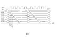
請參照圖3,圖3繪示觸控驅動時脈訊號與顯示驅動時脈訊號於不同運作模式下自動切換的示意圖。Please refer to FIG. 3, which shows a schematic diagram of the touch driving clock signal and the display driving clock signal automatically switching under different operation modes.
如圖3所示,自動切換電路3可包含觸控振盪器31、顯示振盪器32、多工器33及抗尖峰脈衝器34。在第一運作模式(例如顯示休眠模式)MODE1下,多工器33會自動切換至觸控振盪器31並將觸控振盪器31所提供的觸控驅動時脈訊號S1輸出至抗尖峰脈衝器34進行處理後提供為輸出時脈訊號S3。在第二運作模式(例如顯示模式/閒置模式)MODE2下,多工器33會自動切換至顯示振盪器32並將顯示振盪器32所提供的顯示驅動時脈訊號S2輸出至抗尖峰脈衝器34進行處理後提供為輸出時脈訊號S3。As shown in FIG. 3, the
因此,當從第一運作模式(例如顯示休眠模式)MODE1切換至第二運作模式(例如顯示模式/閒置模式)MODE2時,輸出時脈訊號S3亦會從觸控驅動時脈訊號S1變為顯示驅動時脈訊號S2。當從第二運作模式(例如顯示模式/閒置模式)MODE2切換至第一運作模式(例如顯示休眠模式)MODE1時,輸出時脈訊號S3亦會從顯示驅動時脈訊號S2變為觸控驅動時脈訊號S1。Therefore, when switching from the first operating mode (such as display sleep mode) MODE1 to the second operating mode (such as display mode/idle mode) MODE2, the output clock signal S3 will also change from touch drive clock signal S1 to display Drive clock signal S2. When switching from the second operating mode (such as display mode/idle mode) MODE2 to the first operating mode (such as display sleep mode) MODE1, the output clock signal S3 will also change from the display drive clock signal S2 to the touch drive Pulse signal S1.
至於圖4繪示自動切換後之輸出時脈訊號S3於不同運作模式下與觸控驅動時脈訊號S1及顯示驅動時脈訊號S2的對應 關係。As for FIG. 4, the corresponding relationship between the output clock signal S3 after automatic switching and the touch driving clock signal S1 and the display driving clock signal S2 in different operation modes.
如圖4所示,一開始在第二運作模式(例如顯示模式/閒置模式)MODE2下,輸出時脈訊號S3為顯示驅動時脈訊號S2。接著,從第二運作模式(例如顯示模式/閒置模式)MODE2切換至第一運作模式(例如顯示休眠模式)MODE1後,多工器33於時間t進行切換,使得輸出時脈訊號S3開始變為觸控驅動時脈訊號S1。至於從第一運作模式(例如顯示休眠模式)MODE1切換至第三運作模式(例如觸控模式)MODE3後,輸出時脈訊號S3則仍維持觸控驅動時脈訊號S1不變。As shown in FIG. 4, initially in the second operation mode (eg display mode/idle mode) MODE2, the output clock signal S3 is the display driving clock signal S2. Then, after switching from the second operation mode (for example, display mode/idle mode) MODE2 to the first operation mode (for example, display sleep mode) MODE1, the
然而,即使在觸控掃描轉換時序與顯示多工器轉換時序維持一定等距關係的情況下,仍可能因為觸控耦合額外的電壓至顯示而導致顯示不均勻問題,故本發明提出下列方法加以解決:However, even if the touch scan conversion timing and the display multiplexer conversion timing maintain a certain equidistant relationship, the display may still be uneven due to the coupling of additional voltages to the display by the touch. Therefore, the present invention proposes the following method to solve the problem. Solve:
(1)當有機發光二極體觸控顯示裝置進行顯示時,觸控掃描並非在所有顯示時間均進行,而是採用交錯式觸控掃描之方式,亦即在部分的顯示時間進行觸控掃描,但在另一部分的顯示時間停止觸控掃描,藉以有效避免顯示不均勻的現象。(1) When the organic light-emitting diode touch display device performs display, the touch scan is not performed at all the display time, but the interlaced touch scan method is used, that is, the touch scan is performed during part of the display time , But stop the touch scan during another part of the display time to effectively avoid uneven display.
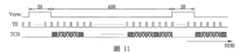
舉例而言,請分別參照圖5至圖8B,圖5至圖8B分別繪示透過交錯式的觸控掃描以避免有機發光二極體觸控顯示裝置之顯示不均勻的不同實施例。其中,Vsync垂直同步訊號,20及400代表顯示線數量,TCH為觸控掃描轉換時序,TE為指示每條顯示線的時脈信號。For example, please refer to FIGS. 5 to 8B respectively. FIGS. 5 to 8B respectively illustrate different embodiments of avoiding uneven display of an organic light-emitting diode touch display device through interlaced touch scanning. Among them, the Vsync vertical synchronization signal, 20 and 400 represent the number of display lines, TCH is the touch scan conversion timing, and TE is the clock signal indicating each display line.
圖5繪示觸控掃描轉換時序TCH僅在有機發光二極體觸控顯示裝置顯示第奇數條顯示線時進行觸控掃描,而在有機發光二極體觸控顯示裝置顯示第偶數條顯示線時則不進行觸控掃描,反之亦然;圖6繪示觸控掃描轉換時序TCH僅在有機發光二極體觸控顯示裝置顯示相鄰的第奇數條顯示線與第偶數條顯示線之間時進行觸控掃描,而在有機發光二極體觸控顯示裝置顯示相鄰的第偶數條顯示線與第奇數條顯示線之間時則不進行觸控掃描,反之亦然。5 shows the touch scan conversion timing TCH only when the organic light-emitting diode touch display device displays the odd-numbered display line, and the organic light-emitting diode touch display device displays the even-numbered display line When the touch scan is not performed, and vice versa; Figure 6 shows the touch scan conversion timing TCH only when the organic light-emitting diode touch display device displays the adjacent odd-numbered display line and the even-numbered display line. When the touch scan is performed when the organic light emitting diode touch display device displays the adjacent even-numbered display line and the odd-numbered display line, the touch scan is not performed, and vice versa.
此外,觸控掃描轉換時序TCH亦可在有機發光二極體觸控顯示裝置進行N條顯示線的觸控掃描後停止M條顯示線不進行觸控掃描,其中N/M大於0。如圖7所示,觸控掃描轉換時序TCH在進行一條顯示線的觸控掃描後停止三條顯示線不進行觸控掃描。如圖8A所示,觸控掃描轉換時序TCH在進行兩條顯示線的觸控掃描後停止兩條顯示線不進行觸控掃描。至於圖8B則是觸控掃描轉換時序TCH在進行一組相鄰的顯示線之間的觸控掃描後停止三組相鄰的顯示線之間不進行觸控掃描,反之亦然。In addition, the touch scan conversion timing TCH can also stop M display lines without touch scan after the organic light emitting diode touch display device performs touch scan of N display lines, where N/M is greater than 0. As shown in FIG. 7, the touch scan conversion timing TCH stops three display lines without performing touch scanning after performing a touch scan of one display line. As shown in FIG. 8A, the touch scan conversion timing TCH stops two display lines without performing touch scanning after performing touch scanning of two display lines. As for FIG. 8B, the touch scan conversion timing TCH stops the touch scan between three groups of adjacent display lines after performing a touch scan between a group of adjacent display lines, and vice versa.
(2)當有機發光二極體觸控顯示裝置進行顯示時,觸控掃描轉換時序TCH可在部分的顯示時間進行觸控掃描,但在另一部分的顯示時間進行觸控電壓補償掃描,藉以有效避免顯示不均勻的現象。如圖9中之觸控掃描轉換時序TCH所示,觸控掃描轉換時序TCH之實線部分代表在部分的顯示時間進行觸控掃描,而觸控掃描轉換時序TCH之虛線部分代表在另一部分的顯示時間進 行觸控電壓補償掃描。(2) When the organic light-emitting diode touch display device performs display, the touch scan conversion timing TCH can perform touch scanning during part of the display time, but perform touch voltage compensation scanning during another part of the display time, so as to be effective Avoid display unevenness. As shown in the touch scan conversion timing TCH in FIG. 9, the solid line part of the touch scan conversion timing TCH represents the touch scan during part of the display time, and the dashed line part of the touch scan conversion timing TCH represents another part of the display time. Display time for touch voltage compensation scan.
圖10至圖13分別繪示透過觸控掃描轉換時序TCH在不同顯示時間分別進行觸控掃描及觸控電壓補償掃描以避免有機發光二極體觸控顯示裝置之顯示不均勻的不同實施例。其中,圖10繪示觸控掃描轉換時序TCH在有機發光二極體觸控顯示裝置顯示第奇數條顯示線時進行觸控掃描(以實線較密集的X表示),而觸控掃描轉換時序TCH在有機發光二極體觸控顯示裝置顯示第偶數條顯示線時則進行觸控電壓補償掃描(以虛線較不密集的X表示),反之亦然。FIGS. 10 to 13 respectively show different embodiments of performing touch scan and touch voltage compensation scan at different display times through the touch scan conversion timing TCH to avoid uneven display of the organic light emitting diode touch display device. 10 shows the touch scan conversion timing TCH when the organic light-emitting diode touch display device displays the odd-numbered display line, the touch scan (indicated by the denser solid line X), and the touch scan conversion timing TCH performs a touch voltage compensation scan when the organic light emitting diode touch display device displays the even-numbered display line (indicated by the less dense dashed X), and vice versa.
此外,觸控掃描轉換時序TCH亦可在進行N條顯示線的觸控掃描(以實線較密集的X表示)後進行M條顯示線的觸控電壓補償掃描(以虛線較不密集的X表示),其中N/M大於0。In addition, the touch scan conversion timing TCH can also be performed after the touch scan of N display lines (indicated by the denser X of the solid line) and then the touch voltage compensation scan of the M display lines (indicated by the less dense X of the dashed line). Means), where N/M is greater than 0.
如圖11所示,觸控掃描轉換時序TCH在進行一條顯示線的觸控掃描(以實線較密集的X表示)後進行三條顯示線的觸控電壓補償掃描(以虛線較不密集的X表示)。如圖12所示,觸控掃描轉換時序TCH在進行兩條顯示線的觸控掃描(以實線較密集的X表示)後進行兩條顯示線的觸控電壓補償掃描(以虛線較不密集的X表示)。至於圖13則是觸控掃描轉換時序TCH在進行一組相鄰的顯示線之間的觸控掃描(以實線較密集的X表示)後進行一組相鄰的顯示線之間的觸控電壓補償掃描(以虛線較不密集的X表示)。As shown in FIG. 11, the touch scan conversion timing TCH performs a touch scan of one display line (indicated by a denser X) and then performs a touch voltage compensation scan of three display lines (indicated by a less dense X Said). As shown in Figure 12, the touch scan conversion timing TCH performs touch scans of two display lines (indicated by X with denser solid lines) and then performs touch voltage compensation scans of two display lines (with less dense dashed lines). The X indicates). As for Figure 13, the touch scan conversion timing TCH performs touch scans between a set of adjacent display lines (indicated by a denser solid line X) and then touches between a set of adjacent display lines. Voltage compensation scan (indicated by the less dense dashed X).
(3)當有機發光二極體觸控顯示裝置進行顯示時,觸控掃描時序與顯示時序須互相搭配,因此,當遇到外部的雜訊 干擾時,觸控掃描轉換時序TCH可將觸控掃描區間移往不會進行顯示的顯示空白(Blanking)區間並調整觸控掃描頻率,以避開外部雜訊之干擾。(3) When the organic light-emitting diode touch display device performs display, the touch scan timing and display timing must match each other. Therefore, when encountering external noise interference, the touch scan conversion timing TCH can change the touch The scan interval is moved to the blanking interval where the display will not be displayed, and the touch scan frequency is adjusted to avoid the interference of external noise.
舉例而言,當遇到外部的雜訊干擾時,觸控掃描轉換時序TCH可自動將觸控掃描區間移往顯示時間之外的顯示空白(Blanking)區間,由於顯示空白區間不會進行顯示,故觸控掃描轉換時序TCH可在此進行連續性的觸控掃描且可以動態改變不同的觸控掃描頻率而不會影響到顯示品質。For example, when encountering external noise interference, the touch scan conversion timing TCH can automatically move the touch scan interval to the blanking interval outside the display time. Since the blanking interval will not be displayed, Therefore, the touch scan conversion timing TCH can perform continuous touch scans and can dynamically change different touch scan frequencies without affecting the display quality.
如圖14A及圖14B所示,當遇到外部雜訊干擾時,觸控掃描轉換時序TCH可自動將觸控掃描區間移往顯示時間之外不會進行顯示的顯示垂直空白(V-Blanking)區間,觸控掃描轉換時序TCH在此進行觸控掃描不會影響到顯示品質。As shown in Figure 14A and Figure 14B, when encountering external noise interference, the touch scan conversion timing TCH can automatically move the touch scan interval beyond the display time and will not display the display vertical blanking (V-Blanking) During the interval, the touch scan conversion timing TCH is performed here for touch scan without affecting the display quality.
如圖15A及圖15B所示,當遇到外部雜訊干擾時,觸控掃描轉換時序TCH可自動將觸控掃描區間從圖15A中顯示多工器轉換時序MUX1~MUX6進行切換的顯示時間移往圖15B中顯示多工器轉換時序MUX1~MUX6不進行切換的顯示垂直空白(V-Blanking)區間,由於顯示垂直空白區間在顯示時間之外而不會進行顯示,故觸控掃描轉換時序TCH可在此進行觸控掃描且可進行觸控掃描頻率之調整,例如從圖15A中之較低的觸控掃描頻率調整為圖15B中之較高的觸控掃描頻率,以避開外部雜訊之干擾。As shown in Figure 15A and Figure 15B, when encountering external noise interference, the touch scan conversion timing TCH can automatically shift the touch scan interval from the display time shift of the multiplexer conversion timing MUX1~MUX6 shown in Figure 15A. Figure 15B shows the multiplexer conversion timing MUX1~MUX6 does not switch the display vertical blanking (V-Blanking) interval, because the display vertical blanking interval is outside the display time and will not be displayed, so the touch scan conversion timing TCH Touch scanning can be performed here and the touch scanning frequency can be adjusted. For example, the touch scanning frequency can be adjusted from a lower touch scanning frequency in FIG. 15A to a higher touch scanning frequency in FIG. 15B to avoid external noise.的interference.
請參照圖16,圖16繪示有機發光二極體觸控顯示裝置運作方法的流程圖。有機發光二極體觸控顯示裝置運作方法係 用以運作有機發光二極體觸控顯示裝置。有機發光二極體觸控顯示裝置係根據觸控掃描轉換時序(Touch scan transition timing)進行觸控掃描並根據顯示多工器轉換時序(Display multiplexer transition timing)進行顯示。如圖16所示,有機發光二極體觸控顯示裝置運作方法包含下列步驟:步驟S10:控制觸控掃描轉換時序與顯示多工器轉換時序維持特定等距關係;步驟S12:當有機發光二極體觸控顯示裝置進行顯示時,有機發光二極體觸控顯示裝置僅於部分的顯示時間進行觸控掃描,而於另一部分的顯示時間停止觸控掃描或進行觸控電壓補償掃描;以及步驟S14:當遇到外部的雜訊干擾時,有機發光二極體觸控顯示裝置僅於顯示時間之外的顯示空白(Blanking)區間進行觸控掃描並可調整觸控掃描頻率,以避開外部雜訊之干擾。Please refer to FIG. 16. FIG. 16 shows a flowchart of an organic light-emitting diode touch display device operation method. The organic light-emitting diode touch display device operation method is used to operate the organic light-emitting diode touch display device. The organic light emitting diode touch display device performs touch scanning according to touch scan transition timing and displays according to display multiplexer transition timing. As shown in FIG. 16, the operation method of the organic light-emitting diode touch display device includes the following steps: Step S10: Control the touch scan conversion timing and the display multiplexer conversion timing to maintain a specific equidistant relationship; Step S12: When the organic light-emitting diode When the polar touch display device performs display, the organic light emitting diode touch display device only performs touch scanning during part of the display time, and stops the touch scanning or performs touch voltage compensation scanning during another part of the display time; and Step S14: When encountering external noise interference, the organic light-emitting diode touch display device only performs touch scanning in the display blanking (Blanking) interval outside the display time and can adjust the touch scanning frequency to avoid Interference from external noise.
相較於先前技術,本發明之有機發光二極體觸控顯示裝置運作方法藉由將觸控掃描轉換時序(Touch scan transition timing)與顯示多工器轉換時序(Display multiplexer transition timing)維持特定等距關係的方式讓觸控模式與顯示模式能夠同時運作,但不會在顯示畫面中出現色帶(Color Band)及閃爍(Flicker)的現象,藉以有效改善有機發光二極體觸控顯示裝置的顯示品質,同時亦可避免觸控掃描時間受限且間隔需拉長以及觸控功耗增加等問題,使得觸控訊雜比獲得提升並可提供更多的充電時 間。Compared with the prior art, the operating method of the organic light emitting diode touch display device of the present invention maintains specific touch scan transition timing and display multiplexer transition timing. The distance relationship allows the touch mode and the display mode to operate at the same time, but no color band and flicker phenomenon appear in the display screen, so as to effectively improve the organic light-emitting diode touch display device The display quality can also avoid problems such as limited touch scan time, longer intervals, and increased touch power consumption, which improves the touch-to-noise ratio and provides more charging time.
由以上較佳具體實施例之詳述,係希望能更加清楚描述本發明之特徵與精神,而並非以上述所揭露的較佳具體實施例來對本發明之範疇加以限制。相反地,其目的是希望能涵蓋各種改變及具相等性的安排於本發明所欲申請之專利範圍的範疇內。藉由以上較佳具體實施例之詳述,係希望能更加清楚描述本發明之特徵與精神,而並非以上述所揭露的較佳具體實施例來對本發明之範疇加以限制。相反地,其目的是希望能涵蓋各種改變及具相等性的安排於本發明所欲申請之專利範圍的範疇內。From the above detailed description of the preferred embodiments, it is hoped that the characteristics and spirit of the present invention can be described more clearly, and the scope of the present invention is not limited by the preferred embodiments disclosed above. On the contrary, the purpose is to cover various changes and equivalent arrangements within the scope of the patent for which the present invention is intended. Based on the above detailed description of the preferred embodiments, it is hoped that the characteristics and spirit of the present invention can be described more clearly, and the scope of the present invention is not limited by the preferred embodiments disclosed above. On the contrary, the purpose is to cover various changes and equivalent arrangements within the scope of the patent for which the present invention is intended.
S10~S14‧‧‧步驟S10~S14‧‧‧Step
Claims (12)
Translated fromChineseApplications Claiming Priority (2)
| Application Number | Priority Date | Filing Date | Title |
|---|---|---|---|
| US201762581083P | 2017-11-03 | 2017-11-03 | |
| US62/581,083 | 2017-11-03 |
Publications (2)
| Publication Number | Publication Date |
|---|---|
| TW201918846A TW201918846A (en) | 2019-05-16 |
| TWI728275Btrue TWI728275B (en) | 2021-05-21 |
Family
ID=66327604
Family Applications (1)
| Application Number | Title | Priority Date | Filing Date |
|---|---|---|---|
| TW107139054ATWI728275B (en) | 2017-11-03 | 2018-11-02 | Organic light-emitting diode touch display operating method |
Country Status (3)
| Country | Link |
|---|---|
| US (1) | US11158685B2 (en) |
| CN (1) | CN109753178B (en) |
| TW (1) | TWI728275B (en) |
Families Citing this family (6)
| Publication number | Priority date | Publication date | Assignee | Title |
|---|---|---|---|---|
| TWI662455B (en)* | 2018-05-31 | 2019-06-11 | 友達光電股份有限公司 | Touch display device and control method thereof |
| CN112259051A (en)* | 2020-11-11 | 2021-01-22 | 上海天马有机发光显示技术有限公司 | Organic light emitting display panel and display device |
| CN113552967A (en)* | 2021-06-24 | 2021-10-26 | 合肥松豪电子科技有限公司 | Touch panel TP frequency hopping scanning method applied to TDDI chip |
| KR20230045735A (en)* | 2021-09-28 | 2023-04-05 | 삼성디스플레이 주식회사 | Display device and driving method thereof |
| CN114485734B (en)* | 2022-04-19 | 2022-06-21 | 宜科(天津)电子有限公司 | Diffuse reflection type photoelectric sensor anti-interference method, equipment and medium |
| CN117971074B (en)* | 2024-04-01 | 2024-07-05 | 深圳贝特莱电子科技股份有限公司 | Main control system supporting touch and display, signal time sequence control method and electronic cigarette |
Citations (7)
| Publication number | Priority date | Publication date | Assignee | Title |
|---|---|---|---|---|
| US20120113045A1 (en)* | 2010-11-05 | 2012-05-10 | Novatek Microelectronics Corp. | Touch controller for touch-sensing display apparatus and driving method thereof |
| US20130069894A1 (en)* | 2011-09-16 | 2013-03-21 | Htc Corporation | Electronic device and method for driving a touch sensor thereof |
| US20140184937A1 (en)* | 2012-12-27 | 2014-07-03 | Lg Display Co., Ltd. | Organic light emitting diode display device including touch panel |
| US20150116266A1 (en)* | 2013-10-29 | 2015-04-30 | Panasonic Intellectual Property Management Co., Ltd. | Input device and display device |
| US20150160761A1 (en)* | 2013-12-09 | 2015-06-11 | Lg Display Co., Ltd. | Touch display device |
| TWI576743B (en)* | 2015-09-30 | 2017-04-01 | 樂金顯示科技股份有限公司 | Multi-touch sensitive display device and method for assigning touch identification therein |
| TWI585730B (en)* | 2006-09-29 | 2017-06-01 | 半導體能源研究所股份有限公司 | Display device and electronic device |
Family Cites Families (34)
| Publication number | Priority date | Publication date | Assignee | Title |
|---|---|---|---|---|
| AU2015203874B2 (en)* | 2006-06-09 | 2016-11-17 | Apple Inc. | Touch screen liquid crystal display |
| JP5523191B2 (en)* | 2010-04-30 | 2014-06-18 | 株式会社ジャパンディスプレイ | Display device with touch detection function |
| TW201205369A (en)* | 2010-07-20 | 2012-02-01 | Novatek Microelectronics Corp | Driving method, driving device and touch sensible display device using the same |
| JP5424347B2 (en)* | 2010-09-17 | 2014-02-26 | 株式会社ジャパンディスプレイ | Display device with touch detection function, driving method thereof, driving circuit, and electronic device |
| CN102999212B (en)* | 2011-09-16 | 2016-08-03 | 宏达国际电子股份有限公司 | Electronic device |
| TWI464642B (en)* | 2012-04-27 | 2014-12-11 | Orise Technology Co Ltd | In-cell multi-touch display panel system |
| JP5922984B2 (en)* | 2012-05-02 | 2016-05-24 | 株式会社ジャパンディスプレイ | Liquid crystal display |
| US9268433B2 (en)* | 2012-06-08 | 2016-02-23 | Apple Inc. | Devices and methods for reducing power usage of a touch-sensitive display |
| CN102768604A (en)* | 2012-06-29 | 2012-11-07 | 京东方科技集团股份有限公司 | A capacitive embedded touch screen, its touch positioning method and display device |
| CN102830879B (en)* | 2012-08-17 | 2015-09-09 | 北京京东方光电科技有限公司 | A kind of In-cell touch panel |
| KR101570455B1 (en)* | 2012-12-19 | 2015-11-19 | 엘지디스플레이 주식회사 | Display device with integrated touch screen and method for driving the same |
| CN103941897B (en)* | 2013-01-23 | 2016-12-28 | 上海天马微电子有限公司 | Embedded touch screen and driving method thereof |
| KR102047825B1 (en)* | 2013-03-06 | 2019-11-22 | 삼성전자 주식회사 | Divided clock generating device and divided clock generating method |
| TWI489363B (en)* | 2013-04-10 | 2015-06-21 | Orise Technology Co Ltd | Method and apparatus for reducing display interference in in-cell touch panel |
| WO2014185523A1 (en)* | 2013-05-17 | 2014-11-20 | シャープ株式会社 | Touch panel system and electronic device |
| JP2015184313A (en)* | 2014-03-20 | 2015-10-22 | シナプティクス・ディスプレイ・デバイス合同会社 | display drive circuit |
| US9164641B1 (en)* | 2014-05-29 | 2015-10-20 | Parade Technologies, Ltd. | In-cell touch scanning modes for simultaneous touch and display |
| JP2016004280A (en)* | 2014-06-13 | 2016-01-12 | 株式会社ジャパンディスプレイ | Touch detection device and display device with touch detection function |
| CN104199573B (en)* | 2014-08-26 | 2017-05-31 | 京东方科技集团股份有限公司 | Touch driving method, touch drive device and touch display screen |
| US9880649B2 (en)* | 2014-09-29 | 2018-01-30 | Apple Inc. | Touch, pen and force sensor operation with variable refresh displays |
| CN104317446B (en)* | 2014-10-15 | 2017-12-29 | 京东方科技集团股份有限公司 | Display device and its driving method |
| CN104461138B (en)* | 2014-12-05 | 2017-07-04 | 京东方科技集团股份有限公司 | The driving method of touch-control display panel, device and touch-control display panel |
| US10048788B2 (en)* | 2015-03-09 | 2018-08-14 | Apple Inc. | Touch screen display uniformity |
| CN104795041B (en)* | 2015-05-08 | 2018-01-23 | 厦门天马微电子有限公司 | A kind of driving method of array base palte, array base palte, display panel and display device |
| CN106325631B (en)* | 2015-07-10 | 2023-03-07 | 宸鸿科技(厦门)有限公司 | A touch display module with pressure detection and its driving method |
| KR102396711B1 (en)* | 2015-09-15 | 2022-05-11 | 엘지전자 주식회사 | Mobile terminal and control method for the mobile terminal |
| US9927910B2 (en)* | 2015-10-30 | 2018-03-27 | Atmel Corporation | Suspension of touch sensor scan based on an expected interference |
| US10324547B2 (en)* | 2015-12-31 | 2019-06-18 | Lg Display Co., Ltd. | Active stylus pen, touch sensing system and driving method thereof |
| US20180040267A1 (en)* | 2016-08-04 | 2018-02-08 | Raydium Semiconductor Corporation | Display apparatus and driving circuit thereof |
| CN106505091B (en)* | 2017-01-04 | 2018-07-17 | 京东方科技集团股份有限公司 | A kind of OLED display panel, production method, driving method and display device |
| KR102284593B1 (en)* | 2017-03-24 | 2021-08-04 | 삼성전자주식회사 | Touch display dirving integrated circuit and operation method thereof |
| KR102374436B1 (en)* | 2017-09-11 | 2022-03-14 | 엘지디스플레이 주식회사 | Touch Device And Method Of Driving The Same |
| JP2019070731A (en)* | 2017-10-10 | 2019-05-09 | シャープ株式会社 | Shift register and display device having the same |
| TW201918850A (en)* | 2017-10-31 | 2019-05-16 | 瑞鼎科技股份有限公司 | In-cell capacitive touch panel |
- 2018
- 2018-11-02TWTW107139054Apatent/TWI728275B/enactive
- 2018-11-02USUS16/178,733patent/US11158685B2/enactiveActive
- 2018-11-02CNCN201811300338.3Apatent/CN109753178B/enactiveActive
Patent Citations (7)
| Publication number | Priority date | Publication date | Assignee | Title |
|---|---|---|---|---|
| TWI585730B (en)* | 2006-09-29 | 2017-06-01 | 半導體能源研究所股份有限公司 | Display device and electronic device |
| US20120113045A1 (en)* | 2010-11-05 | 2012-05-10 | Novatek Microelectronics Corp. | Touch controller for touch-sensing display apparatus and driving method thereof |
| US20130069894A1 (en)* | 2011-09-16 | 2013-03-21 | Htc Corporation | Electronic device and method for driving a touch sensor thereof |
| US20140184937A1 (en)* | 2012-12-27 | 2014-07-03 | Lg Display Co., Ltd. | Organic light emitting diode display device including touch panel |
| US20150116266A1 (en)* | 2013-10-29 | 2015-04-30 | Panasonic Intellectual Property Management Co., Ltd. | Input device and display device |
| US20150160761A1 (en)* | 2013-12-09 | 2015-06-11 | Lg Display Co., Ltd. | Touch display device |
| TWI576743B (en)* | 2015-09-30 | 2017-04-01 | 樂金顯示科技股份有限公司 | Multi-touch sensitive display device and method for assigning touch identification therein |
Also Published As
| Publication number | Publication date |
|---|---|
| US11158685B2 (en) | 2021-10-26 |
| US20190140024A1 (en) | 2019-05-09 |
| TW201918846A (en) | 2019-05-16 |
| CN109753178A (en) | 2019-05-14 |
| CN109753178B (en) | 2022-07-12 |
Similar Documents
| Publication | Publication Date | Title |
|---|---|---|
| TWI728275B (en) | Organic light-emitting diode touch display operating method | |
| CN103855192B (en) | A kind of AMOLED display device and image element driving method thereof | |
| TWI647603B (en) | Touch display device driving method, touch display control device and touch display control method | |
| TWI521493B (en) | Electronic device and timing control method thereof | |
| US11144126B2 (en) | Touch display device, driving method, and driving circuit | |
| CN114241993B (en) | Driving circuit, driving method thereof, and display panel | |
| US20180121023A1 (en) | Gate driver and display device having in-cell touch sensor using the same | |
| CN102651196B (en) | Drive circuit and drive method of AMOLED (Active Matrix Organic Light-Emitting Diode), and display device | |
| KR20160081702A (en) | Data controling circuit and flat panel display device | |
| CN103714784A (en) | Liquid crystal display device including TFT compensation circuit | |
| US12277913B2 (en) | Display device including timing controller that operates display panel in low speed mode, display panel, and display driving method | |
| JP2013168083A (en) | Detection device, detection method, and electronic apparatus | |
| CN104078006A (en) | Pixel circuit, display panel and display device | |
| WO2017107746A1 (en) | Gip circuit and driving method therefor, and flat panel display device | |
| US20170132978A1 (en) | Display device and driving method for the same | |
| TWI885641B (en) | Display apparatus and driving method thereof | |
| US9589498B2 (en) | Display driver and display device | |
| CN113053287A (en) | Display device | |
| CN103426398B (en) | Organic light emitting diode display and driving method thereof | |
| CN105654902A (en) | OLED display panel, touch electrode driving circuit and driving method | |
| CN114203109B (en) | Pixel driving circuit, compensation method thereof and display panel | |
| JP4440559B2 (en) | Display device | |
| KR102023547B1 (en) | Display device and driving method thereof | |
| KR102416710B1 (en) | Touch display device and driving method for the same | |
| KR102837849B1 (en) | Display device and driving method |