TWI726125B - Semiconductor device and method of manufacturing the same - Google Patents
Semiconductor device and method of manufacturing the sameDownload PDFInfo
- Publication number
- TWI726125B TWI726125BTW106122311ATW106122311ATWI726125BTW I726125 BTWI726125 BTW I726125BTW 106122311 ATW106122311 ATW 106122311ATW 106122311 ATW106122311 ATW 106122311ATW I726125 BTWI726125 BTW I726125B
- Authority
- TW
- Taiwan
- Prior art keywords
- top surface
- insulating film
- isolation region
- element isolation
- gate electrode
- Prior art date
Links
- 239000004065semiconductorSubstances0.000titleclaimsabstractdescription248
- 238000004519manufacturing processMethods0.000titleclaimsdescription73
- 230000015654memoryEffects0.000claimsabstractdescription225
- 238000002955isolationMethods0.000claimsabstractdescription187
- 239000000758substrateSubstances0.000claimsabstractdescription95
- VYPSYNLAJGMNEJ-UHFFFAOYSA-NSilicium dioxideChemical compoundO=[Si]=OVYPSYNLAJGMNEJ-UHFFFAOYSA-N0.000claimsdescription58
- 229910052814silicon oxideInorganic materials0.000claimsdescription56
- 238000000034methodMethods0.000claimsdescription45
- 229910052581Si3N4Inorganic materials0.000claimsdescription39
- HQVNEWCFYHHQES-UHFFFAOYSA-Nsilicon nitrideChemical compoundN12[Si]34N5[Si]62N3[Si]51N64HQVNEWCFYHHQES-UHFFFAOYSA-N0.000claimsdescription39
- 238000001312dry etchingMethods0.000claimsdescription24
- 238000005530etchingMethods0.000claimsdescription7
- 239000013078crystalSubstances0.000claimsdescription2
- 230000006872improvementEffects0.000abstractdescription2
- 239000010410layerSubstances0.000description55
- 239000011229interlayerSubstances0.000description34
- 238000009792diffusion processMethods0.000description31
- 229910021420polycrystalline siliconInorganic materials0.000description30
- 229920005591polysiliconPolymers0.000description30
- 229910052751metalInorganic materials0.000description25
- 239000002184metalSubstances0.000description25
- 238000005229chemical vapour depositionMethods0.000description19
- 239000012535impuritySubstances0.000description19
- 229910021332silicideInorganic materials0.000description16
- FVBUAEGBCNSCDD-UHFFFAOYSA-Nsilicide(4-)Chemical compound[Si-4]FVBUAEGBCNSCDD-UHFFFAOYSA-N0.000description16
- 229920002120photoresistant polymerPolymers0.000description15
- 229910021417amorphous siliconInorganic materials0.000description12
- 238000001039wet etchingMethods0.000description12
- 238000003860storageMethods0.000description11
- 230000015572biosynthetic processEffects0.000description10
- 230000003647oxidationEffects0.000description10
- 238000007254oxidation reactionMethods0.000description10
- 230000004048modificationEffects0.000description7
- 238000012986modificationMethods0.000description7
- 230000000694effectsEffects0.000description6
- 239000002784hot electronSubstances0.000description6
- 238000002347injectionMethods0.000description6
- 239000007924injectionSubstances0.000description6
- 150000004767nitridesChemical class0.000description6
- 230000005641tunnelingEffects0.000description6
- 239000004020conductorSubstances0.000description5
- 238000005468ion implantationMethods0.000description5
- 238000005498polishingMethods0.000description5
- OAICVXFJPJFONN-UHFFFAOYSA-NPhosphorusChemical compound[P]OAICVXFJPJFONN-UHFFFAOYSA-N0.000description4
- 229910052785arsenicInorganic materials0.000description4
- RQNWIZPPADIBDY-UHFFFAOYSA-Narsenic atomChemical compound[As]RQNWIZPPADIBDY-UHFFFAOYSA-N0.000description4
- 238000000059patterningMethods0.000description4
- 229910052698phosphorusInorganic materials0.000description4
- 239000011574phosphorusSubstances0.000description4
- 239000010936titaniumSubstances0.000description4
- 229910018072Al 2 O 3Inorganic materials0.000description3
- PXHVJJICTQNCMI-UHFFFAOYSA-NNickelChemical compound[Ni]PXHVJJICTQNCMI-UHFFFAOYSA-N0.000description3
- 229910052782aluminiumInorganic materials0.000description3
- XAGFODPZIPBFFR-UHFFFAOYSA-NaluminiumChemical compound[Al]XAGFODPZIPBFFR-UHFFFAOYSA-N0.000description3
- 230000004888barrier functionEffects0.000description3
- 239000010941cobaltSubstances0.000description3
- 229910017052cobaltInorganic materials0.000description3
- GUTLYIVDDKVIGB-UHFFFAOYSA-Ncobalt atomChemical compound[Co]GUTLYIVDDKVIGB-UHFFFAOYSA-N0.000description3
- TWNQGVIAIRXVLR-UHFFFAOYSA-Noxo(oxoalumanyloxy)alumaneChemical compoundO=[Al]O[Al]=OTWNQGVIAIRXVLR-UHFFFAOYSA-N0.000description3
- 238000004544sputter depositionMethods0.000description3
- ZOXJGFHDIHLPTG-UHFFFAOYSA-NBoronChemical compound[B]ZOXJGFHDIHLPTG-UHFFFAOYSA-N0.000description2
- 240000004050Pentaglottis sempervirensSpecies0.000description2
- 235000004522Pentaglottis sempervirensNutrition0.000description2
- XUIMIQQOPSSXEZ-UHFFFAOYSA-NSiliconChemical compound[Si]XUIMIQQOPSSXEZ-UHFFFAOYSA-N0.000description2
- RTAQQCXQSZGOHL-UHFFFAOYSA-NTitaniumChemical compound[Ti]RTAQQCXQSZGOHL-UHFFFAOYSA-N0.000description2
- NRTOMJZYCJJWKI-UHFFFAOYSA-NTitanium nitrideChemical compound[Ti]#NNRTOMJZYCJJWKI-UHFFFAOYSA-N0.000description2
- MCMNRKCIXSYSNV-UHFFFAOYSA-NZrO2Inorganic materialsO=[Zr]=OMCMNRKCIXSYSNV-UHFFFAOYSA-N0.000description2
- UQZIWOQVLUASCR-UHFFFAOYSA-Nalumane;titaniumChemical compound[AlH3].[Ti]UQZIWOQVLUASCR-UHFFFAOYSA-N0.000description2
- 238000000231atomic layer depositionMethods0.000description2
- 229910052796boronInorganic materials0.000description2
- 230000008859changeEffects0.000description2
- 239000000470constituentSubstances0.000description2
- 230000005684electric fieldEffects0.000description2
- 230000005669field effectEffects0.000description2
- 230000006870functionEffects0.000description2
- CJNBYAVZURUTKZ-UHFFFAOYSA-Nhafnium(iv) oxideChemical compoundO=[Hf]=OCJNBYAVZURUTKZ-UHFFFAOYSA-N0.000description2
- 230000012447hatchingEffects0.000description2
- 238000010438heat treatmentMethods0.000description2
- 238000009413insulationMethods0.000description2
- MRELNEQAGSRDBK-UHFFFAOYSA-Nlanthanum(3+);oxygen(2-)Chemical compound[O-2].[O-2].[O-2].[La+3].[La+3]MRELNEQAGSRDBK-UHFFFAOYSA-N0.000description2
- 239000000463materialSubstances0.000description2
- 229910044991metal oxideInorganic materials0.000description2
- 150000004706metal oxidesChemical class0.000description2
- PEUPIGGLJVUNEU-UHFFFAOYSA-Nnickel siliconChemical compound[Si].[Ni]PEUPIGGLJVUNEU-UHFFFAOYSA-N0.000description2
- BPUBBGLMJRNUCC-UHFFFAOYSA-Noxygen(2-);tantalum(5+)Chemical compound[O-2].[O-2].[O-2].[O-2].[O-2].[Ta+5].[Ta+5]BPUBBGLMJRNUCC-UHFFFAOYSA-N0.000description2
- RVTZCBVAJQQJTK-UHFFFAOYSA-Noxygen(2-);zirconium(4+)Chemical compound[O-2].[O-2].[Zr+4]RVTZCBVAJQQJTK-UHFFFAOYSA-N0.000description2
- 229910052710siliconInorganic materials0.000description2
- 239000010703siliconSubstances0.000description2
- 229910052719titaniumInorganic materials0.000description2
- WFKWXMTUELFFGS-UHFFFAOYSA-NtungstenChemical compound[W]WFKWXMTUELFFGS-UHFFFAOYSA-N0.000description2
- 229910052721tungstenInorganic materials0.000description2
- 239000010937tungstenSubstances0.000description2
- 229910004129HfSiOInorganic materials0.000description1
- BPQQTUXANYXVAA-UHFFFAOYSA-NOrthosilicateChemical compound[O-][Si]([O-])([O-])[O-]BPQQTUXANYXVAA-UHFFFAOYSA-N0.000description1
- QVGXLLKOCUKJST-UHFFFAOYSA-Natomic oxygenChemical compound[O]QVGXLLKOCUKJST-UHFFFAOYSA-N0.000description1
- 229910021419crystalline siliconInorganic materials0.000description1
- 238000000151depositionMethods0.000description1
- 229910052735hafniumInorganic materials0.000description1
- VBJZVLUMGGDVMO-UHFFFAOYSA-Nhafnium atomChemical compound[Hf]VBJZVLUMGGDVMO-UHFFFAOYSA-N0.000description1
- 239000007943implantSubstances0.000description1
- 238000002513implantationMethods0.000description1
- 239000012212insulatorSubstances0.000description1
- 229910021421monocrystalline siliconInorganic materials0.000description1
- 229910052759nickelInorganic materials0.000description1
- 230000001590oxidative effectEffects0.000description1
- 229910052760oxygenInorganic materials0.000description1
- 239000001301oxygenSubstances0.000description1
- 230000000149penetrating effectEffects0.000description1
- 239000000377silicon dioxideSubstances0.000description1
- 238000009751slip formingMethods0.000description1
- 239000000126substanceSubstances0.000description1
- 238000006557surface reactionMethods0.000description1
Images


Classifications
- H—ELECTRICITY
- H10—SEMICONDUCTOR DEVICES; ELECTRIC SOLID-STATE DEVICES NOT OTHERWISE PROVIDED FOR
- H10B—ELECTRONIC MEMORY DEVICES
- H10B43/00—EEPROM devices comprising charge-trapping gate insulators
- H10B43/30—EEPROM devices comprising charge-trapping gate insulators characterised by the memory core region
- H—ELECTRICITY
- H01—ELECTRIC ELEMENTS
- H01L—SEMICONDUCTOR DEVICES NOT COVERED BY CLASS H10
- H01L21/00—Processes or apparatus adapted for the manufacture or treatment of semiconductor or solid state devices or of parts thereof
- H01L21/70—Manufacture or treatment of devices consisting of a plurality of solid state components formed in or on a common substrate or of parts thereof; Manufacture of integrated circuit devices or of parts thereof
- H01L21/71—Manufacture of specific parts of devices defined in group H01L21/70
- H01L21/76—Making of isolation regions between components
- H01L21/762—Dielectric regions, e.g. EPIC dielectric isolation, LOCOS; Trench refilling techniques, SOI technology, use of channel stoppers
- H01L21/76224—Dielectric regions, e.g. EPIC dielectric isolation, LOCOS; Trench refilling techniques, SOI technology, use of channel stoppers using trench refilling with dielectric materials
- H—ELECTRICITY
- H10—SEMICONDUCTOR DEVICES; ELECTRIC SOLID-STATE DEVICES NOT OTHERWISE PROVIDED FOR
- H10B—ELECTRONIC MEMORY DEVICES
- H10B43/00—EEPROM devices comprising charge-trapping gate insulators
- H10B43/30—EEPROM devices comprising charge-trapping gate insulators characterised by the memory core region
- H10B43/35—EEPROM devices comprising charge-trapping gate insulators characterised by the memory core region with cell select transistors, e.g. NAND
- H—ELECTRICITY
- H10—SEMICONDUCTOR DEVICES; ELECTRIC SOLID-STATE DEVICES NOT OTHERWISE PROVIDED FOR
- H10B—ELECTRONIC MEMORY DEVICES
- H10B43/00—EEPROM devices comprising charge-trapping gate insulators
- H10B43/40—EEPROM devices comprising charge-trapping gate insulators characterised by the peripheral circuit region
- H—ELECTRICITY
- H10—SEMICONDUCTOR DEVICES; ELECTRIC SOLID-STATE DEVICES NOT OTHERWISE PROVIDED FOR
- H10D—INORGANIC ELECTRIC SEMICONDUCTOR DEVICES
- H10D30/00—Field-effect transistors [FET]
- H10D30/01—Manufacture or treatment
- H10D30/021—Manufacture or treatment of FETs having insulated gates [IGFET]
- H10D30/0413—Manufacture or treatment of FETs having insulated gates [IGFET] of FETs having charge-trapping gate insulators, e.g. MNOS transistors
- H—ELECTRICITY
- H10—SEMICONDUCTOR DEVICES; ELECTRIC SOLID-STATE DEVICES NOT OTHERWISE PROVIDED FOR
- H10D—INORGANIC ELECTRIC SEMICONDUCTOR DEVICES
- H10D30/00—Field-effect transistors [FET]
- H10D30/60—Insulated-gate field-effect transistors [IGFET]
- H10D30/62—Fin field-effect transistors [FinFET]
- H10D30/6211—Fin field-effect transistors [FinFET] having fin-shaped semiconductor bodies integral with the bulk semiconductor substrates
- H—ELECTRICITY
- H10—SEMICONDUCTOR DEVICES; ELECTRIC SOLID-STATE DEVICES NOT OTHERWISE PROVIDED FOR
- H10D—INORGANIC ELECTRIC SEMICONDUCTOR DEVICES
- H10D30/00—Field-effect transistors [FET]
- H10D30/60—Insulated-gate field-effect transistors [IGFET]
- H10D30/62—Fin field-effect transistors [FinFET]
- H10D30/6217—Fin field-effect transistors [FinFET] having non-uniform gate electrodes, e.g. gate conductors having varying doping
- H—ELECTRICITY
- H10—SEMICONDUCTOR DEVICES; ELECTRIC SOLID-STATE DEVICES NOT OTHERWISE PROVIDED FOR
- H10D—INORGANIC ELECTRIC SEMICONDUCTOR DEVICES
- H10D30/00—Field-effect transistors [FET]
- H10D30/60—Insulated-gate field-effect transistors [IGFET]
- H10D30/69—IGFETs having charge trapping gate insulators, e.g. MNOS transistors
- H10D30/694—IGFETs having charge trapping gate insulators, e.g. MNOS transistors characterised by the shapes, relative sizes or dispositions of the gate electrodes
- H10D30/696—IGFETs having charge trapping gate insulators, e.g. MNOS transistors characterised by the shapes, relative sizes or dispositions of the gate electrodes having at least one additional gate, e.g. program gate, erase gate or select gate
- H—ELECTRICITY
- H10—SEMICONDUCTOR DEVICES; ELECTRIC SOLID-STATE DEVICES NOT OTHERWISE PROVIDED FOR
- H10D—INORGANIC ELECTRIC SEMICONDUCTOR DEVICES
- H10D30/00—Field-effect transistors [FET]
- H10D30/60—Insulated-gate field-effect transistors [IGFET]
- H10D30/69—IGFETs having charge trapping gate insulators, e.g. MNOS transistors
- H10D30/694—IGFETs having charge trapping gate insulators, e.g. MNOS transistors characterised by the shapes, relative sizes or dispositions of the gate electrodes
- H10D30/697—IGFETs having charge trapping gate insulators, e.g. MNOS transistors characterised by the shapes, relative sizes or dispositions of the gate electrodes having trapping at multiple separated sites, e.g. multi-particles trapping sites
- H—ELECTRICITY
- H10—SEMICONDUCTOR DEVICES; ELECTRIC SOLID-STATE DEVICES NOT OTHERWISE PROVIDED FOR
- H10D—INORGANIC ELECTRIC SEMICONDUCTOR DEVICES
- H10D64/00—Electrodes of devices having potential barriers
- H10D64/01—Manufacture or treatment
- H10D64/031—Manufacture or treatment of data-storage electrodes
- H10D64/037—Manufacture or treatment of data-storage electrodes comprising charge-trapping insulators
- H—ELECTRICITY
- H10—SEMICONDUCTOR DEVICES; ELECTRIC SOLID-STATE DEVICES NOT OTHERWISE PROVIDED FOR
- H10D—INORGANIC ELECTRIC SEMICONDUCTOR DEVICES
- H10D84/00—Integrated devices formed in or on semiconductor substrates that comprise only semiconducting layers, e.g. on Si wafers or on GaAs-on-Si wafers
- H10D84/01—Manufacture or treatment
- H10D84/0123—Integrating together multiple components covered by H10D12/00 or H10D30/00, e.g. integrating multiple IGBTs
- H10D84/0126—Integrating together multiple components covered by H10D12/00 or H10D30/00, e.g. integrating multiple IGBTs the components including insulated gates, e.g. IGFETs
- H10D84/0158—Integrating together multiple components covered by H10D12/00 or H10D30/00, e.g. integrating multiple IGBTs the components including insulated gates, e.g. IGFETs the components including FinFETs
- H—ELECTRICITY
- H10—SEMICONDUCTOR DEVICES; ELECTRIC SOLID-STATE DEVICES NOT OTHERWISE PROVIDED FOR
- H10D—INORGANIC ELECTRIC SEMICONDUCTOR DEVICES
- H10D84/00—Integrated devices formed in or on semiconductor substrates that comprise only semiconducting layers, e.g. on Si wafers or on GaAs-on-Si wafers
- H10D84/01—Manufacture or treatment
- H10D84/02—Manufacture or treatment characterised by using material-based technologies
- H10D84/03—Manufacture or treatment characterised by using material-based technologies using Group IV technology, e.g. silicon technology or silicon-carbide [SiC] technology
- H10D84/038—Manufacture or treatment characterised by using material-based technologies using Group IV technology, e.g. silicon technology or silicon-carbide [SiC] technology using silicon technology, e.g. SiGe
- H—ELECTRICITY
- H10—SEMICONDUCTOR DEVICES; ELECTRIC SOLID-STATE DEVICES NOT OTHERWISE PROVIDED FOR
- H10D—INORGANIC ELECTRIC SEMICONDUCTOR DEVICES
- H10D84/00—Integrated devices formed in or on semiconductor substrates that comprise only semiconducting layers, e.g. on Si wafers or on GaAs-on-Si wafers
- H10D84/80—Integrated devices formed in or on semiconductor substrates that comprise only semiconducting layers, e.g. on Si wafers or on GaAs-on-Si wafers characterised by the integration of at least one component covered by groups H10D12/00 or H10D30/00, e.g. integration of IGFETs
- H10D84/82—Integrated devices formed in or on semiconductor substrates that comprise only semiconducting layers, e.g. on Si wafers or on GaAs-on-Si wafers characterised by the integration of at least one component covered by groups H10D12/00 or H10D30/00, e.g. integration of IGFETs of only field-effect components
- H10D84/83—Integrated devices formed in or on semiconductor substrates that comprise only semiconducting layers, e.g. on Si wafers or on GaAs-on-Si wafers characterised by the integration of at least one component covered by groups H10D12/00 or H10D30/00, e.g. integration of IGFETs of only field-effect components of only insulated-gate FETs [IGFET]
- H10D84/834—Integrated devices formed in or on semiconductor substrates that comprise only semiconducting layers, e.g. on Si wafers or on GaAs-on-Si wafers characterised by the integration of at least one component covered by groups H10D12/00 or H10D30/00, e.g. integration of IGFETs of only field-effect components of only insulated-gate FETs [IGFET] comprising FinFETs
- H—ELECTRICITY
- H10—SEMICONDUCTOR DEVICES; ELECTRIC SOLID-STATE DEVICES NOT OTHERWISE PROVIDED FOR
- H10D—INORGANIC ELECTRIC SEMICONDUCTOR DEVICES
- H10D64/00—Electrodes of devices having potential barriers
- H10D64/01—Manufacture or treatment
- H10D64/017—Manufacture or treatment using dummy gates in processes wherein at least parts of the final gates are self-aligned to the dummy gates, i.e. replacement gate processes
Landscapes
- Engineering & Computer Science (AREA)
- Physics & Mathematics (AREA)
- Condensed Matter Physics & Semiconductors (AREA)
- General Physics & Mathematics (AREA)
- Manufacturing & Machinery (AREA)
- Computer Hardware Design (AREA)
- Microelectronics & Electronic Packaging (AREA)
- Power Engineering (AREA)
- Semiconductor Memories (AREA)
- Non-Volatile Memory (AREA)
- Metal-Oxide And Bipolar Metal-Oxide Semiconductor Integrated Circuits (AREA)
- Insulated Gate Type Field-Effect Transistor (AREA)
Abstract
Description
Translated fromChinese本發明係關於一種半導體裝置及其製造方法,例如可適當利用在具有以鰭(Fin)狀的半導體部構成之鰭式電晶體(Fin Field Effect Transistor,FINFET)的半導體裝置及其製造。The present invention relates to a semiconductor device and a manufacturing method thereof. For example, a semiconductor device having a Fin Field Effect Transistor (FINFET) composed of a fin-shaped semiconductor portion can be suitably used and the manufacturing method thereof.
例如於美國專利申請公開第2015/0270401號說明書(專利文獻1)記載一種FINFET,在至少2種不同半導體材料形成有通道區。For example, US Patent Application Publication No. 2015/0270401 (Patent Document 1) describes a FINFET in which channel regions are formed in at least two different semiconductor materials.
此外,於美國專利申請公開第2014/0346612號說明書(專利文獻2),記載藉由熱氧化、電漿氧化或氧離子注入而形成將複數之鰭彼此分離之元件隔離區的技術,元件隔離區之頂面成為凸形。 [習知技術文獻] [專利文獻]In addition, in the specification of US Patent Application Publication No. 2014/0346612 (Patent Document 2), it is described that the device isolation region is formed by thermal oxidation, plasma oxidation, or oxygen ion implantation to separate a plurality of fins from each other. The top surface becomes convex. [Related Technical Documents] [Patent Documents]
專利文獻1:美國專利申請公開第2015/0270401號說明書 專利文獻2:美國專利申請公開第2014/0346612號說明書Patent Document 1: U.S. Patent Application Publication No. 2015/0270401 Specification Patent Document 2: U.S. Patent Application Publication No. 2014/0346612 Specification
[本發明所欲解決的問題] 16nm節點以下之具有鰭式通道的分離閘極式記憶體單元中,彼此相鄰的記憶體單元之間的距離接近,而有通過連結記憶體單元間的捕集性絕緣膜(電荷儲存膜、電荷保存膜)之電荷的擴散,對記憶體單元的可靠度造成影響之顧慮。[Problem to be solved by the present invention] In the separated gate memory cell with fin channel below the 16nm node, the distance between the adjacent memory cells is close, and there is a trap by connecting the memory cells. There is a concern that the diffusion of charges in the collective insulating film (charge storage film, charge storage film) will affect the reliability of the memory cell.
其他問題與新特徵,應可自本說明書之記述內容及附圖明瞭。 [解決問題之技術手段]Other issues and new features should be clear from the description of this manual and the drawings. [Technical means to solve the problem]
一實施形態之半導體裝置,設置有複數之鰭,其係半導體基板之一部分,在沿著半導體基板之主面的第1方向延伸,且在沿著半導體基板之主面而與第1方向直交的第2方向彼此分隔。此外,於在第2方向彼此相鄰的鰭之間,元件隔離區之頂面的一部分位於較連結面更高之位置,該連結面,將與一方的鰭之側壁接觸的元件隔離區之頂面的位置、和與另一方的鰭之側壁接觸的元件隔離區之頂面的位置連結;在沿著第2方向的剖面中,元件隔離區之頂面成為凸形。The semiconductor device of one embodiment is provided with a plurality of fins, which are a part of the semiconductor substrate, extend in the first direction along the main surface of the semiconductor substrate, and are perpendicular to the first direction along the main surface of the semiconductor substrate The second directions are separated from each other. In addition, between the fins adjacent to each other in the second direction, a part of the top surface of the device isolation region is located at a higher position than the connection surface, and the connection surface will be the top of the device isolation region that contacts the sidewall of one fin The position of the surface is connected to the position of the top surface of the element isolation region in contact with the side wall of the other fin; in the cross section along the second direction, the top surface of the element isolation region becomes convex.
一實施形態之半導體裝置之製造方法,包含如下步驟:氮化膜形成步驟,於半導體基板之主面上,形成氮化膜;以及突出部形成步驟,將氮化膜及半導體基板依序加工,形成複數之溝槽,藉而形成由半導體基板之一部分構成的複數之突出部,複數之突出部在沿著半導體基板之主面的第1方向延伸,且在沿著半導體基板之主面而與第1方向直交的第2方向彼此分隔。更包含如下步驟:氧化膜嵌入步驟,於半導體基板之主面上沉積氧化膜,以氧化膜嵌入複數之溝槽的內部;平坦化步驟,將氧化膜之頂面及氮化膜之頂面平坦化;氮化膜去除步驟,去除氮化膜;以及突出部露出步驟,施行等向性乾蝕刻,使氧化膜之頂面及側面分別後退,從氧化膜之頂面露出複數之突出部之頂面及側壁。此外,於在第2方向彼此相鄰的突出部之間,氧化膜之頂面的一部分位於較連結面更高之位置,該連結面,將與一方的突出部之側壁接觸的氧化膜之頂面的位置、和與另一方的突出部之側壁接觸的氧化膜之頂面的位置連結;在沿著第2方向的剖面中,使氧化膜之頂面呈凸形。 [本發明之效果]A method of manufacturing a semiconductor device according to an embodiment includes the following steps: a nitride film forming step of forming a nitride film on the main surface of a semiconductor substrate; and a protrusion forming step of sequentially processing the nitride film and the semiconductor substrate, A plurality of grooves are formed, thereby forming a plurality of protrusions composed of a part of the semiconductor substrate, and the plurality of protrusions extend in the first direction along the main surface of the semiconductor substrate, and are connected with each other along the main surface of the semiconductor substrate. The second directions orthogonal to the first direction are separated from each other. It further includes the following steps: an oxide film embedding step, depositing an oxide film on the main surface of the semiconductor substrate, and embedding the oxide film inside the plurality of trenches; a planarization step, flattening the top surface of the oxide film and the top surface of the nitride film Nitride film removal step, the nitride film is removed; and the protrusion exposure step is to perform isotropic dry etching to make the top and side surfaces of the oxide film recede, and expose the top of the plurality of protrusions from the top surface of the oxide film Surface and side wall. In addition, between the protrusions adjacent to each other in the second direction, a part of the top surface of the oxide film is located higher than the connecting surface, and the connecting surface will be the top of the oxide film in contact with the side wall of one protrusion The position of the surface is connected to the position of the top surface of the oxide film in contact with the side wall of the other protrusion; in the cross section along the second direction, the top surface of the oxide film is convex. [Effects of the invention]
依照一實施形態,可改善半導體裝置的可靠度。According to one embodiment, the reliability of the semiconductor device can be improved.
以下實施形態中,雖為了方便在必要時分割為複數之個部分或實施形態予以說明,但除了特別指出之情況以外,其等並非彼此全無關聯,而係具有一方為另一方之部分或全部的變形例、細節、補充說明等關係。In the following embodiment, although it is divided into plural parts or embodiments for convenience when necessary, they are not completely unrelated to each other, except for cases specifically pointed out, but have one part or all of the other. Modifications, details, supplementary explanations and other relations of.
此外,以下實施形態中,在提及要素的數目等(包括個數、數值、量、範圍等)之情況,除了特別指出之情況及原理上明顯限定為特定數目之情況等以外,並未限定為該特定數目,可為特定數目以上亦可為以下。In addition, in the following embodiments, when referring to the number of elements (including number, numerical value, amount, range, etc.), it is not limited except for the cases specifically pointed out and the cases where the principle is clearly limited to a specific number, etc. The specific number may be greater than or less than the specific number.
此外,以下實施形態中,其構成要素(亦包括要素步驟等),除了特別指出之情況及原理上明顯被視為必須之情況等以外,自然可說是並非為必要。In addition, in the following embodiments, its constituent elements (including element steps, etc.) are naturally not necessary except for cases specifically pointed out and cases that are clearly deemed necessary in principle.
此外,提及「由A構成」、「以A形成」、「具有A」、「包含A」時,除了特別指出僅為該要素之情況等,自然未指排除其以外之要素。同樣地,以下實施形態中,在提及構成要素等之形狀、位置關係等時,除了特別指出之情況及原理上明顯被視為並非如此之情況等以外,包含實質上與該形狀等近似或類似者等。此一條件,對於上述數目及範圍亦相同。In addition, when referring to "consisting of A", "formed by A", "having A", and "including A", except for the case where only the element is specified, it naturally does not mean that the other elements are excluded. Similarly, in the following embodiments, when referring to the shape, positional relationship, etc. of the constituent elements, etc., except for the cases specifically pointed out and the cases that are obviously not the case in principle, etc., it includes substantially similar or similar to the shape, etc. Similar ones and so on. This condition is the same for the above-mentioned number and range.
此外,在用於說明以下實施形態的全部附圖中,對具有同一功能者原則上給予同一符號,並省略其重複的說明。此外,在剖面圖及俯視圖中,各部位之大小並未與實際裝置對應,為了使附圖容易理解,而有將特定部位相對放大顯示之情況。此外,在剖面圖與俯視圖對應之情況中,為了使附圖容易理解,而有將特定部位相對放大顯示之情況。此外,有即便為剖面圖仍為了容易觀看附圖而將影線省略之情況,亦有即便為俯視圖仍為了容易觀看附圖而附加影線之情況。In addition, in all the drawings for explaining the following embodiments, those having the same function are given the same reference numerals in principle, and repeated descriptions thereof are omitted. In addition, in the cross-sectional view and the plan view, the size of each part does not correspond to the actual device. In order to make the drawings easy to understand, a specific part may be relatively enlarged and displayed. In addition, in the case where the cross-sectional view corresponds to the plan view, in order to make the drawing easier to understand, a specific part may be relatively enlarged and displayed. In addition, there are cases where hatching is omitted for easy viewing of the drawings even if it is a cross-sectional view, and there are cases where hatching is added for easy viewing of the drawings even if it is a plan view.
以下,依據附圖詳細地說明本實施形態。Hereinafter, this embodiment will be described in detail with reference to the drawings.
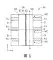
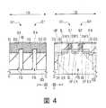
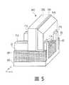
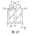
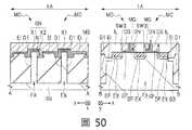
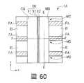
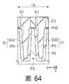
(實施形態1) <半導體裝置的構造> 利用圖1~圖5,對本實施形態1之半導體裝置的構造予以說明。圖1為,顯示本實施形態1之半導體裝置的記憶體單元區之俯視圖。圖2為,顯示本實施形態1之半導體裝置的邏輯區之俯視圖。圖3為,顯示本實施形態1之半導體裝置的記憶體單元區之沿著圖1的A-A線及B-B線之剖面圖。圖4為,顯示本實施形態1之半導體裝置的邏輯區之沿著圖2的C-C線及D-D線之剖面圖。圖5為,本實施形態1之半導體裝置的形成於記憶體單元區之記憶體單元的鳥瞰圖。(Embodiment 1) <Structure of semiconductor device> The structure of the semiconductor device of the first embodiment will be described with reference to FIGS. 1 to 5. FIG. 1 is a plan view showing the memory cell area of the semiconductor device of the first embodiment. FIG. 2 is a plan view showing the logic area of the semiconductor device of the first embodiment. FIG. 3 is a cross-sectional view showing the memory cell region of the semiconductor device of the first embodiment along the AA line and the BB line in FIG. 1. 4 is a cross-sectional view showing the logic area of the semiconductor device of the first embodiment along the CC line and the DD line of FIG. 2. 5 is a bird's-eye view of the memory cell formed in the memory cell area of the semiconductor device of the first embodiment.
圖3所示的沿著A-A線之剖面,係沿著記憶體單元區的鰭上方之閘極電極的延伸方向之剖面;沿著B-B線之剖面,係沿著記憶體單元區之鰭的延伸方向之剖面。圖4所示的沿著C-C之剖面,係沿著邏輯區的鰭上方之閘極電極的延伸方向之剖面;沿著D-D線之剖面,係沿著邏輯區之鰭的延伸方向之剖面。另,圖1及圖2中,省略源極/汲極區、層間絕緣膜、各閘極電極上之矽化物層等的圖示。進一步,圖5中,省略側壁的圖示。The cross-section along the line AA shown in FIG. 3 is along the extending direction of the gate electrode above the fin of the memory cell area; the cross-section along the line BB is along the memory cell area The section of the fin in the direction of extension. The cross section along CC shown in Figure 4 is along the extension direction of the gate electrode above the fins in the logic area; the cross section along the DD line is along the extension direction of the fins in the logic area的profile. In addition, in FIGS. 1 and 2, illustrations of source/drain regions, interlayer insulating films, and silicide layers on each gate electrode are omitted. Furthermore, in FIG. 5, illustration of the side wall is omitted.
本實施形態1之半導體裝置,於同一半導體晶片上,搭載有由2個FINFET構成之分離閘極式記憶體單元、及例如低耐受電壓之n型FINFET。記憶體單元配置於記憶體單元區,低耐受電壓之FINFET配置於邏輯區。記憶體單元區及邏輯區,係在沿著半導體基板之主面的方向排列之區域。In the semiconductor device of the first embodiment, a separate gate type memory cell composed of two FINFETs and, for example, an n-type FINFET with a low withstand voltage are mounted on the same semiconductor chip. The memory cell is arranged in the memory cell area, and the FINFET with low withstand voltage is arranged in the logic area. The memory cell area and the logic area are areas arranged in the direction along the main surface of the semiconductor substrate.
如圖1、圖3及圖5的記憶體單元區1A所示,記憶體單元(未揮發性儲存元件)MC,形成於板狀的鰭FA之上部,該板狀的鰭FA為半導體基板SB之一部分,形成於半導體基板SB之上部。此外,如圖2及圖4的邏輯區1B所示,係低耐受電壓之FINFET的電晶體Q1,形成於板狀的鰭FB之上部,該板狀的鰭FB為半導體基板SB之一部分,形成於半導體基板SB之上部。As shown in the
鰭FA、FB,各自為沿著沿半導體基板SB之主面的x方向(第1方向)而延伸之半導體層的圖案;對x方向直交,沿著半導體基板SB之主面的y方向(第2方向)中之鰭FA、FB的各自之寬度,較x方向之鰭FA、FB的各自之寬度明顯更小。半導體基板SB,例如由單晶矽構成。The fins FA and FB are each a pattern of a semiconductor layer extending along the x direction (first direction) along the main surface of the semiconductor substrate SB; orthogonal to the x direction, along the y direction (first direction) of the main surface of the semiconductor substrate SB The respective widths of the fins FA and FB in the 2 direction) are significantly smaller than the respective widths of the fins FA and FB in the x direction. The semiconductor substrate SB is made of, for example, single crystal silicon.
鰭FA、FB,分別在y方向彼此分隔而排列配置複數之。圖1及圖2中,雖僅分別顯示3個在y方向排列的鰭FA、FB,但鰭FA、FB,亦可分別在y方向中進一步排列配置多個。The fins FA and FB are separated from each other in the y direction and arranged in plural. In FIGS. 1 and 2, although only three fins FA and FB arranged in the y direction are shown, respectively, a plurality of fins FA and FB may be further arranged in the y direction.
此外,記憶體單元區1A,亦可在x方向中亦排列配置複數之鰭FA,若為具有長度、寬度及高度之突出部,則未要求其形狀。例如亦包含俯視時曲折的圖案。此外,亦未要求鰭FA之排列方式。同樣地,邏輯區1B,亦可在x方向中排列配置複數之鰭FB,若為具有長度、寬度及高度之突出部,則未要求其形狀。例如亦包含俯視時曲折的圖案。此外,亦未要求鰭FB之排列方式。In addition, the
於複數之鰭FA彼此之間形成溝槽D1,該溝槽D1形成於半導體基板SB之頂面。於複數之鰭FB彼此之間形成溝槽D2,該溝槽D2形成於半導體基板SB之頂面。A trench D1 is formed between the plurality of fins FA, and the trench D1 is formed on the top surface of the semiconductor substrate SB. A trench D2 is formed between the plurality of fins FB, and the trench D2 is formed on the top surface of the semiconductor substrate SB.
如圖3所示,在y方向彼此相鄰的2個鰭FA之彼此的端部,藉由係半導體基板SB之一部分的被元件隔離區EI覆蓋之下部圖案UP而連接。另,下部圖案UP,若從該2個鰭FA之彼此的端部往y方向延伸,與鰭FA連接,則未要求其形狀。同樣地,如圖4所示,在y方向彼此相鄰的2個鰭FB之彼此的端部,藉由係半導體基板SB之一部分的被元件隔離區EI覆蓋之下部圖案UP而連接。另,下部圖案UP,若從該2個鰭FB之彼此的端部往y方向延伸,與鰭FB連接,則未要求其形狀。As shown in FIG. 3, the ends of two fins FA adjacent to each other in the y-direction are connected by a part of the semiconductor substrate SB covered by the lower part pattern UP by the element isolation region EI. In addition, if the lower pattern UP extends in the y direction from the ends of the two fins FA and is connected to the fin FA, its shape is not required. Similarly, as shown in FIG. 4, the ends of the two fins FB adjacent to each other in the y direction are connected by a part of the semiconductor substrate SB covered by the lower part pattern UP of the element isolation region EI. In addition, if the lower pattern UP extends in the y direction from the ends of the two fins FB and is connected to the fin FB, its shape is not required.
鰭FA、及與鰭FA連接的下部圖案UP之各自的側壁,構成溝槽D1的側壁。此外,鰭FB、及與鰭FB連接的下部圖案UP之各自的側壁,構成溝槽D2的側壁。亦可不形成與各個鰭FA、FB連接之下部圖案UP。亦即,形成有下部圖案UP之區域,亦可為嵌入至各個溝槽D1、D2的元件隔離區EI之一部分。The respective sidewalls of the fin FA and the lower pattern UP connected to the fin FA constitute the sidewall of the trench D1. In addition, the respective sidewalls of the fin FB and the lower pattern UP connected to the fin FB constitute the sidewall of the trench D2. It is not necessary to form the lower part pattern UP connected to the respective fins FA and FB. That is, the region where the lower pattern UP is formed may also be a part of the element isolation region EI embedded in the trenches D1 and D2.
如圖3及圖4所示,元件隔離區EI,係嵌入至各個溝槽D1、D2之絕緣膜。然則,元件隔離區EI並未完全嵌入各個溝槽D1、D2,鰭FA、FB之各自的一部分在元件隔離區EI之頂面上突出。從元件隔離區EI之頂面露出的鰭FA、FB之各自的高度,例如為40nm~60nm程度。元件隔離區EI,覆蓋下部圖案UP之全體。元件隔離區EI,例如由氧化矽構成。As shown in FIGS. 3 and 4, the element isolation region EI is embedded in the insulating film of each trench D1, D2. However, the element isolation region EI is not completely embedded in each trench D1, D2, and a part of each of the fins FA and FB protrudes on the top surface of the element isolation region EI. The respective heights of the fins FA and FB exposed from the top surface of the element isolation region EI are, for example, about 40 nm to 60 nm. The element isolation area EI covers the entire lower pattern UP. The element isolation region EI is made of silicon oxide, for example.
本實施形態1中,將係記憶體單元區1A之構成半導體基板SB的一部分之圖案的包含上層圖案與下層圖案之板狀的半導體層,稱作鰭FA:該上層圖案,從元件隔離區EI露出,在x方向延伸;該下層圖案,在該上層圖案的正下方中,從該上層圖案側到達至溝槽D1之底部。同樣地,將係邏輯區1B之構成半導體基板SB的一部分之圖案的包含上層圖案與下層圖案之板狀的半導體層,稱作鰭FB:該上層圖案,從元件隔離區EI露出,在x方向延伸;該下層圖案,在該上層圖案的正下方中,從該上層圖案側到達至溝槽D2之底部。In the first embodiment, a plate-shaped semiconductor layer including an upper layer pattern and a lower layer pattern, which is a pattern constituting a part of the semiconductor substrate SB in the
亦即,鰭,係在半導體基板SB之頂面中往半導體基板SB的上方突出之半導體圖案,例如為圖1及圖2之在x方向延伸的突出部。此處,以下部圖案UP並非鰭FA、FB之各自的一部分之態樣進行說明。雖未圖示,但在鰭FA、FB之各自的頂面,將包含p型雜質(例如硼(B))之p型井,形成於較後述源極/汲極區更為深層。That is, the fin is a semiconductor pattern that protrudes above the semiconductor substrate SB from the top surface of the semiconductor substrate SB, and is, for example, a protrusion extending in the x direction in FIGS. 1 and 2. Here, description will be given of the aspect in which the lower pattern UP is not a part of each of the fins FA and FB. Although not shown, on the top surfaces of the fins FA and FB, p-type wells containing p-type impurities (for example, boron (B)) are formed in a deeper layer than the source/drain regions described later.
如圖3及圖5所示,記憶體單元區1A中,元件隔離區EI之頂面在沿著y方向的剖面中成為凸形。換而言之,則於在y方向彼此相鄰的鰭FA之間,元件隔離區EI之頂面的一部分位於較連結面更高之位置,該連結面,將與一方的鰭FA之側壁接觸的元件隔離區EI之頂面的位置、和與另一方的鰭FA之側壁接觸的元件隔離區EI之頂面的位置連結。As shown in FIGS. 3 and 5, in the
然則,若元件隔離區EI之頂面的凸部之高度過高,則元件隔離區EI之頂面的段差變大,形成元件隔離區EI後之加工處理變得困難。因此,元件隔離區EI之頂面的凸部之高度,例如宜為20nm~30nm程度,例如若使在y方向彼此相鄰的鰭FA之間隔為a,使凸部之高度為b,則b/a宜為0.2~0.5程度。此處,凸部之高度,係於在y方向彼此相鄰的鰭FA之間,從連結面至元件隔離區EI之頂面的最高位置之距離,而該連結面,將與一方的鰭FA之側壁接觸的元件隔離區EI之頂面的位置、和與另一方的鰭FA之側壁接觸的元件隔離區EI之頂面的位置連結。However, if the height of the convex portion on the top surface of the element isolation region EI is too high, the step difference of the top surface of the element isolation region EI becomes larger, and the processing after the formation of the element isolation region EI becomes difficult. Therefore, the height of the convex portion on the top surface of the element isolation region EI is preferably about 20 nm to 30 nm, for example, if the distance between the fins FA adjacent to each other in the y direction is a, and the height of the convex portion is b, then b /A is preferably about 0.2 to 0.5. Here, the height of the convex portion is the distance between the fins FA adjacent to each other in the y-direction from the connection surface to the highest position of the top surface of the element isolation region EI, and the connection surface will be connected to one of the fins FA The position of the top surface of the element isolation region EI contacting the sidewall of the fin FA is connected to the position of the top surface of the element isolation region EI contacting the sidewall of the other fin FA.
如此地,藉由使記憶體單元區1A的元件隔離區EI之頂面呈凸形,相較於元件隔離區EI之頂面為平坦形狀的情況,在y方向彼此相鄰的記憶體單元MC間之中,構成後述ONO膜(Oxide-Nitride-Oxide)膜ON的捕集性絕緣膜之路徑變長,故可抑制電荷擴散的影響。In this way, by making the top surface of the device isolation region EI of the
另一方面,如圖4所示,邏輯區1B中,在y方向彼此相鄰的鰭FB之間隔,例如為50nm以下之小間隔的情況,元件隔離區EI之頂面在沿著y方向的剖面中並未成為凸形,而成為幾近平坦。亦即,邏輯區1B的元件隔離區EI之頂面的平面度,較記憶體單元區1A的元件隔離區EI之頂面的平面度成為更小。On the other hand, as shown in FIG. 4, in the
相對於此,在y方向彼此相鄰的鰭FB之間隔,例如為60nm以上之大間隔的情況,元件隔離區EI之頂面在沿著y方向的剖面中成為凸形。然則,邏輯區1B,不具有如在記憶體單元區1A中發生的電荷擴散之問題,此外,若於元件隔離區EI之頂面具有凸部,則邏輯區1B的形成元件隔離區EI後之加工處理變得困難,因而宜使元件隔離區EI之頂面平坦。In contrast, when the interval between the fins FB adjacent to each other in the y direction is a large interval of, for example, 60 nm or more, the top surface of the element isolation region EI becomes convex in the cross section along the y direction. However, the
如圖1、圖3及圖5所示,記憶體單元區1A中,於在y方向排列之複數之鰭FA的正上方,以橫跨此等鰭FA之方式,形成有在y方向延伸的控制閘極電極CG、及在y方向延伸的記憶體閘極電極MG。As shown in FIGS. 1, 3, and 5, in the
控制閘極電極CG,隔著閘極絕緣膜GF而形成於從元件隔離區EI之頂面露出的鰭FA之頂面及側壁。閘極絕緣膜GF,例如由氧化矽構成;控制閘極電極CG,例如由多晶矽構成。The control gate electrode CG is formed on the top surface and sidewalls of the fin FA exposed from the top surface of the element isolation region EI via the gate insulating film GF. The gate insulating film GF is made of, for example, silicon oxide; the control gate electrode CG is made of, for example, polysilicon.
x方向的控制閘極電極CG之一方的側壁由側壁SW3覆蓋,於另一方的側壁,隔著ONO膜ON而形成記憶體閘極電極MG。側壁SW3,例如由氮化矽、氧化矽或其等之疊層膜構成。ONO膜ON為,從半導體基板SB側及控制閘極電極CG側起,依序疊層有氧化矽膜X1、氮化矽膜N1及氧化矽膜X2的疊層膜;記憶體閘極電極MG,例如由多晶矽構成。氮化矽膜N1為捕集性絕緣膜(電荷儲存膜、電荷保存膜),藉由以記憶體單元MC之操作改變氮化矽膜N1的電荷貯存狀態,而可改變記憶體單元MC的閾值電壓。One side wall of the control gate electrode CG in the x direction is covered by the side wall SW3, and on the other side wall, the memory gate electrode MG is formed with the ONO film ON interposed therebetween. The sidewall SW3 is made of, for example, silicon nitride, silicon oxide, or a laminated film thereof. The ONO film ON is a laminated film in which a silicon oxide film X1, a silicon nitride film N1, and a silicon oxide film X2 are sequentially stacked from the semiconductor substrate SB side and the control gate electrode CG side; the memory gate electrode MG , For example, made of polysilicon. The silicon nitride film N1 is a trapping insulating film (charge storage film, charge storage film). By operating the memory cell MC to change the charge storage state of the silicon nitride film N1, the threshold value of the memory cell MC can be changed Voltage.
記憶體閘極電極MG,隔著ONO膜ON而形成於從元件隔離區EI之頂面露出的鰭FA之頂面及側壁。亦即,ONO膜ON,具有沿著鰭FA的頂面、控制閘極電極CG的側壁而連續形成之L字形的剖面。記憶體閘極電極MG,藉由ONO膜ON,而與控制閘極電極CG及鰭FA絕緣。The memory gate electrode MG is formed on the top surface and sidewalls of the fin FA exposed from the top surface of the element isolation region EI via the ONO film ON. That is, the ONO film ON has a zigzag cross-section formed continuously along the top surface of the fin FA and the sidewall of the control gate electrode CG. The memory gate electrode MG is insulated from the control gate electrode CG and the fin FA by the ONO film ON.
係x方向之記憶體閘極電極MG的側壁之未與ONO膜ON接觸的側壁,由側壁SW3覆蓋。於控制閘極電極CG及記憶體閘極電極MG的各自之頂面,形成矽化物層SI。矽化物層SI,例如由鎳矽化物(NiSi)或鈷矽化物(CoSi)構成。矽化物層SI,係為了降低分別對控制閘極電極CG之頂面及記憶體閘極電極MG之頂面連接的接觸栓塞(未圖示),與控制閘極電極CG或記憶體閘極電極MG之連接電阻而設置。The sidewalls of the sidewalls of the memory gate electrode MG in the x direction that are not in contact with the ONO film ON are covered by the sidewall SW3. A silicide layer SI is formed on the respective top surfaces of the control gate electrode CG and the memory gate electrode MG. The silicide layer SI is made of nickel silicide (NiSi) or cobalt silicide (CoSi), for example. The silicide layer SI is to reduce the contact plugs (not shown) connected to the top surface of the control gate electrode CG and the top surface of the memory gate electrode MG, respectively, and are connected to the control gate electrode CG or the memory gate electrode Set the connection resistance of MG.
於記憶體單元區1A的鰭FA之正上方,將包含隔著ONO膜ON而彼此鄰接之控制閘極電極CG及記憶體閘極電極MG的圖案,在x方向排列而形成一對。該一對圖案彼此分隔,於構成該一對圖案的2個控制閘極電極CG彼此之相對向的面,與記憶體閘極電極MG鄰接。Just above the fin FA of the
於x方向的該圖案旁邊之兩側的鰭FA之頂面,形成一對源極/汲極區。源極/汲極區,分別由導入有n型雜質(例如磷(P)或砷(As))的2個n型半導體區構成,亦即由延伸區EX及擴散層DF構成。延伸區EX,為n型雜質之濃度較擴散層DF更低的區域。此處,將延伸區EX形成於較擴散層DF更為深層。此外,延伸區EX,配置於相較於鄰接之擴散層DF,更為接近控制閘極電極CG及記憶體閘極電極MG之各自的正下方之位置。如此地,該源極/汲極區,具有包含雜質濃度低的延伸區EX、及雜質濃度高的擴散層DF之LDD(Lightly Doped Drain,淺摻雜汲極)構造。On the top surfaces of the fins FA on both sides beside the pattern in the x direction, a pair of source/drain regions are formed. The source/drain regions are respectively composed of two n-type semiconductor regions into which n-type impurities (such as phosphorus (P) or arsenic (As)) are introduced, that is, are composed of an extension region EX and a diffusion layer DF. The extension region EX is a region where the concentration of n-type impurities is lower than that of the diffusion layer DF. Here, the extension region EX is formed in a deeper layer than the diffusion layer DF. In addition, the extension region EX is arranged at a position that is closer to the position directly below each of the control gate electrode CG and the memory gate electrode MG than the adjacent diffusion layer DF. In this way, the source/drain region has an LDD (Lightly Doped Drain) structure including an extension region EX with a low impurity concentration and a diffusion layer DF with a high impurity concentration.
控制閘極電極CG、及形成於該控制閘極電極CG之兩側的鰭FA之頂面的一對源極/汲極區,構成MISFET(Metal Insulator Semiconductor Field Effect Transistor,金屬絕緣半導體場效電晶體)構造之第1電晶體(控制用電晶體)。此外,記憶體閘極電極MG、及形成於該記憶體閘極電極MG之兩側的鰭FA之頂面的一對源極/汲極區,構成MISFET構造之第2電晶體(記憶體用電晶體)。本實施形態1之1個記憶體單元MC,係由彼此共用源極/汲極區的第1電晶體與第2電晶體所構成。亦即,記憶體單元MC,具有控制閘極電極CG、記憶體閘極電極MG、ONO膜ON、控制閘極電極CG附近的汲極區、及記憶體閘極電極MG附近的源極區。The control gate electrode CG and a pair of source/drain regions on the top surface of the fin FA formed on both sides of the control gate electrode CG constitute a MISFET (Metal Insulator Semiconductor Field Effect Transistor). Crystal) structure of the first transistor (control transistor). In addition, the memory gate electrode MG and a pair of source/drain regions on the top surface of the fin FA formed on both sides of the memory gate electrode MG constitute the second transistor of the MISFET structure (for memory Transistor). One memory cell MC in the first embodiment is composed of a first transistor and a second transistor that share a source/drain region with each other. That is, the memory cell MC has a control gate electrode CG, a memory gate electrode MG, an ONO film ON, a drain region near the control gate electrode CG, and a source region near the memory gate electrode MG.
於1個鰭FA上,形成2個記憶體單元MC。該2個記憶體單元MC,共用彼此的源極區。控制閘極電極CG及記憶體閘極電極MG之各自的正下方的鰭FA之頂面,包含在記憶體單元MC操作時形成通道的通道區。該通道,為鰭式通道。記憶體單元MC,為可進行寫入操作及抹除操作之電性改寫的非揮發性記憶體。On one fin FA, two memory cells MC are formed. The two memory cells MC share the source region of each other. The top surface of the fin FA directly below each of the control gate electrode CG and the memory gate electrode MG includes a channel area that forms a channel when the memory cell MC is operating. This channel is a fin channel. The memory cell MC is a non-volatile memory that can be electrically rewritten for writing and erasing operations.
此外,如圖2及圖4所示,邏輯區1B中,於在y方向排列之複數之鰭FB的正上方,以橫跨此等鰭FB之方式,形成有在y方向延伸的閘極電極G1。In addition, as shown in FIGS. 2 and 4, in the
閘極電極G1,隔著閘極絕緣膜GI而形成於從元件隔離區EI之頂面露出的鰭FB之頂面及側壁。The gate electrode G1 is formed on the top surface and sidewalls of the fin FB exposed from the top surface of the element isolation region EI via the gate insulating film GI.
此外,閘極絕緣膜GI,連續地覆蓋閘極電極G1的底面及兩側的側壁。亦即,閘極電極G1,其頂面以外的面被閘極絕緣膜GI包圍。另,雖未圖示,但在閘極絕緣膜GI與鰭FB之間,作為閘極絕緣膜GI的一部分,例如亦可形成氧化矽膜。閘極絕緣膜GI,例如可使用二氧化鉿(HfO2)膜、二氧化鋯(ZrO2)膜、氧化鋁(Al2O3)膜、氧化鉭(Ta2O5)膜或氧化鑭(La2O3)膜等金屬氧化物膜。閘極絕緣膜GI,為介電常數較氧化矽膜更高之所謂的high-k膜。In addition, the gate insulating film GI continuously covers the bottom surface and the side walls on both sides of the gate electrode G1. That is, the surface of the gate electrode G1 other than the top surface is surrounded by the gate insulating film GI. Although not shown, a silicon oxide film may be formed between the gate insulating film GI and the fin FB as a part of the gate insulating film GI, for example. As the gate insulating film GI, for example, a hafnium dioxide (HfO2 ) film, a zirconium dioxide (ZrO2 ) film, an aluminum oxide (Al2 O3 ) film, a tantalum oxide (Ta2 O5 ) film, or a lanthanum oxide ( La2 O3 ) film and other metal oxide films. The gate insulating film GI is a so-called high-k film with a higher dielectric constant than a silicon oxide film.
閘極電極G1,例如由鋁(Al)構成。此外,閘極電極G1,例如亦可具有在半導體基板SB上依序疊層有鈦鋁(TiAl)及鋁(Al)而構成之疊層構造。The gate electrode G1 is made of aluminum (Al), for example. In addition, the gate electrode G1 may have a laminated structure in which titanium aluminum (TiAl) and aluminum (Al) are sequentially laminated on the semiconductor substrate SB, for example.
x方向的閘極電極G1之兩側的側壁由側壁SW3覆蓋。於閘極電極G1之頂面,並未形成矽化物層SI。在將閘極電極G1、與其上方之接觸栓塞(未圖示)連接的情況,由金屬膜構成之閘極電極G1相較於矽膜為低電阻,故即便未經由矽化物層SI仍可將閘極電極G1與接觸栓塞歐姆連接。The side walls on both sides of the gate electrode G1 in the x direction are covered by the side walls SW3. No silicide layer SI is formed on the top surface of the gate electrode G1. In the case of connecting the gate electrode G1 to the contact plug (not shown) above it, the gate electrode G1 made of a metal film has a lower resistance than a silicon film, so even if it is not made of a silicide layer SI, the gate electrode G1 can still be connected The gate electrode G1 is ohmically connected to the contact plug.
於邏輯區1B的鰭FB之正上方,在x方向排列而形成一對閘極電極G1。該一對閘極電極G1彼此分隔。Just above the fin FB of the
於x方向的閘極電極G1旁邊之兩側的鰭FB之頂面,形成一對源極/汲極區。源極/汲極區,與記憶體單元區1A的源極/汲極區同樣地,分別由導入有n型雜質(例如磷(P)或砷(As))的2個n型半導體區構成,亦即由延伸區EX及擴散層DF構成。另,邏輯區1B的源極/汲極區之雜質濃度,較記憶體單元區1A的源極/汲極區之雜質濃度更低。A pair of source/drain regions are formed on the top surfaces of the fins FB on both sides next to the gate electrode G1 in the x direction. The source/drain regions, similar to the source/drain regions of the
閘極電極G1、及形成於該閘極電極G1之兩側的鰭FB之頂面的一對源極/汲極區,構成具有MISFET構造之低耐受電壓的電晶體Q1。The gate electrode G1 and a pair of source/drain regions on the top surface of the fin FB formed on both sides of the gate electrode G1 constitute a low withstand voltage transistor Q1 having a MISFET structure.
於1個鰭FB上,形成2個電晶體Q1。閘極電極G1之正下方的鰭FB之頂面,包含在電晶體Q1操作時形成通道的通道區。該通道,為鰭式通道。此外,2個電晶體Q1,共用彼此具有的一對源極/汲極區中之一方。On one fin FB, two transistors Q1 are formed. The top surface of the fin FB directly below the gate electrode G1 includes a channel region that forms a channel when the transistor Q1 is operating. This channel is a fin channel. In addition, the two transistors Q1 share one of the pair of source/drain regions.
本實施形態1中,將具有鰭FA之一部分作為通道區,且形成於鰭FA之上部的上述第1電晶體、第2電晶體、以及電晶體Q1,稱作FINFET。構成記憶體單元MC之第1電晶體與第2電晶體,相較於構成邏輯電路之低耐受電壓的電晶體Q1,係以高電壓驅動的電晶體,故相較於電晶體Q1要求高耐受電壓性能。In the first embodiment, the first transistor, the second transistor, and the transistor Q1 described above that have a part of the fin FA as the channel region and are formed on the upper portion of the fin FA are called FINFETs. Compared with the low withstand voltage transistor Q1 that constitutes the logic circuit, the first transistor and the second transistor constituting the memory cell MC are driven by a higher voltage, so the requirements are higher than those of the transistor Q1 Withstand voltage performance.
此外,如圖3及圖4所示,記憶體單元區1A及邏輯區1B中,元件隔離區EI的頂面、鰭FA與鰭FB之各自的頂面及側壁、與側壁SW3的側壁等,由層間絕緣膜IL覆蓋。層間絕緣膜IL,例如由氧化矽構成。另,雖未圖示,但在層間絕緣膜IL,和元件隔離區EI的頂面、鰭FA與鰭FB之各自的頂面及側壁、與側壁SW3的側壁之間,形成薄層絕緣膜;該絕緣膜,例如由氮化矽構成。使層間絕緣膜IL、側壁SW3、閘極電極G1、ONO膜ON、控制閘極電極CG及記憶體閘極電極MG之各自的頂面,在大致相同的的平面中平坦化。In addition, as shown in FIGS. 3 and 4, in the
雖未圖示,但層間絕緣膜IL、記憶體單元MC及電晶體Q1之各自的上部,由層間絕緣膜覆蓋。此外,雖未圖示,但形成貫通層間絕緣膜IL、及層間絕緣膜IL上之該層間絕緣膜的複數之接觸栓塞;接觸栓塞,與閘極電極G1、控制閘極電極CG、記憶體閘極電極MG及各源極/汲極區電性連接。此外,雖未圖示,但於接觸栓塞上形成配線。Although not shown, the upper portions of the interlayer insulating film IL, the memory cell MC, and the transistor Q1 are covered by the interlayer insulating film. In addition, although not shown, a plurality of contact plugs are formed penetrating the interlayer insulating film IL and the interlayer insulating film on the interlayer insulating film IL; the contact plugs are connected to the gate electrode G1, the control gate electrode CG, and the memory gate. The electrode MG and each source/drain area are electrically connected. In addition, although not shown, wiring is formed on the contact plug.
<半導體裝置之特徵及效果> 本實施形態1之半導體裝置的主要特徵,在於使記憶體單元區1A的元件隔離區EI之頂面呈凸形的點。<Characteristics and Effects of Semiconductor Device> The main feature of the semiconductor device of the first embodiment is to make the top surface of the element isolation region EI of the
16nm節點以下之分離閘極式記憶體單元MC,在y方向彼此相鄰的記憶體單元MC之間的距離變小,在y方向彼此相鄰的記憶體單元MC分別具有之ONO膜ON的距離變近。因此,吾人認為,電荷通過構成ONO膜ON之係捕集性絕緣膜的氮化矽膜N1而擴散,對記憶體單元MC的可靠度造成影響。For the separated gate memory cell MC below the 16nm node, the distance between the adjacent memory cells MC in the y direction becomes smaller, and the ONO film ON distance of the memory cells MC adjacent to each other in the y direction. Getting closer. Therefore, we believe that the charge diffuses through the silicon nitride film N1 that constitutes the trapping insulating film of the ONO film ON, which affects the reliability of the memory cell MC.
然則,本實施形態1之半導體裝置,藉由使記憶體單元區1A的元件隔離區EI之頂面呈凸形,而將在y方向彼此相鄰的記憶體單元MC之間的氮化矽膜N1(捕集性絕緣膜)之路徑增長。亦即,形成有凸部的情況,相較於未形成凸部的情況,氮化矽膜N1之路徑變長,電荷之擴散距離變長,故可抑制經由在y方向彼此相鄰的記憶體單元MC之間的氮化矽膜N1之路徑的資料變動。藉此,可改善半導體裝置的可靠度。However, in the semiconductor device of the first embodiment, by making the top surface of the element isolation region EI of the
<半導體裝置之動作> 對於本實施形態1之半導體裝置中的以非揮發性記憶體為主之動作予以說明。<The operation of the semiconductor device> The operation of the semiconductor device of the first embodiment mainly based on the non-volatile memory will be described.
本實施形態1之記憶體單元,具有MISFET構造,使在MISFET的閘極電極內之捕集性絕緣膜的電荷貯存狀態為儲存資訊,讀取其等以作為MISFET的閾值。捕集性絕緣膜,係指可貯存電荷的絕緣膜,作為一例,可列舉氮化矽膜等。藉由電荷對此等電荷貯存區的注入/放出而使MISFET的閾值偏移,使其作為儲存元件而操作。作為使用捕集性絕緣膜之未揮發性半導體儲存裝置,如同本實施形態1之記憶體單元地,具有分離閘極式之MONOS(Metal-Oxide-Nitride-Oxide-Semiconductor,金屬氧化氮氧化物半導體)記憶體。The memory cell of the first embodiment has a MISFET structure, and the charge storage state of the trapping insulating film in the gate electrode of the MISFET is stored as information, and this is read as the threshold value of the MISFET. The trapping insulating film refers to an insulating film that can store charges, and as an example, a silicon nitride film or the like can be cited. The threshold value of the MISFET is shifted by the injection/discharge of electric charge into the charge storage area, so that it can operate as a storage element. As a non-volatile semiconductor storage device using a trapping insulating film, like the memory cell of the first embodiment, MONOS (Metal-Oxide-Nitride-Oxide-Semiconductor) has a separate gate type. )Memory.
作為施行記憶體單元之「寫入」及「抹除」的操作法,具有例如SSI(Source Side Injection,源極側注入)方式、BTBT(Band To Band Tunneling,能帶間穿隧)方式及FN(Fowler Nordheim)方式等。As the operation method of "write" and "erase" of the memory cell, there are, for example, SSI (Source Side Injection) method, BTBT (Band To Band Tunneling) method and FN (Fowler Nordheim) method and so on.
SSI方式,可視作藉由對捕集性絕緣膜注入熱電子而施行記憶體單元之寫入的操作法;BTBT方式,可視作藉由對捕集性絕緣膜注入熱電洞而施行記憶體單元之抹除的操作法;FN方式,可視作藉由電子或電洞的穿隧而施行寫入或抹除的操作法。關於FN方式,若以其他表現方式說明,則FN方式之寫入,可視作藉由以FN穿隧效應將電子注入捕集性絕緣膜而施行記憶體單元之寫入的操作方式;FN方式之抹除,可視作對藉由以FN穿隧效應將電洞注入捕集性絕緣膜而施行記憶體單元之抹除的操作方式。The SSI method can be regarded as an operation method of performing memory cell writing by injecting hot electrons into the trapping insulating film; the BTBT method can be regarded as the operation method of performing memory cell writing by injecting thermoelectric holes into the trapping insulating film. Erase operation method; the FN method can be regarded as an operation method for writing or erasing by tunneling electrons or holes. Regarding the FN method, if it is described in other ways of expression, the FN method of writing can be regarded as an operation method of performing the writing of the memory cell by injecting electrons into the trapping insulating film by the FN tunneling effect; The erasure can be regarded as an operation method for erasing the memory cell by injecting holes into the trapping insulating film by the FN tunneling effect.
以下,對於施行SSI方式所產生的寫入,並施行FN方式所產生的抹除之情況予以說明。亦即,將對捕集性絕緣膜(例如圖3所示的絕緣膜ONO膜ON中的係電荷貯存部之氮化矽膜N1)之電子的注入定義為「寫入」,將電洞的注入定義為「抹除」。In the following, a description will be given of the case where the writing by the SSI method is performed and the erasing by the FN method is performed. That is, the injection of electrons into the trapping insulating film (for example, the silicon nitride film N1 of the charge storage portion in the insulating film ONO film ON shown in FIG. 3) is defined as "writing", and the hole Injection is defined as "erasing".
SSI方式之寫入,對施行寫入之選擇記憶體單元的各部位分別施加寫入操作電壓,將熱電子注入選擇記憶體單元之捕集性絕緣膜中藉而施行寫入。In SSI writing, a writing operation voltage is applied to each part of the selected memory cell for writing, and hot electrons are injected into the trapping insulating film of the selected memory cell to perform writing.
此時,熱電子,在2個閘極電極(記憶體閘極電極MG及控制閘極電極CG)間的下方之通道區(源極、汲極間)產生,將熱電子注入記憶體閘極電極MG下方之捕集性絕緣膜。注入的熱電子,在捕集性絕緣膜中之陷阱能階捕獲,此一結果,選擇電晶體的閾值電壓上升。亦即,選擇電晶體成為寫入狀態。At this time, hot electrons are generated in the channel area (between the source and drain) between the two gate electrodes (memory gate electrode MG and control gate electrode CG), and hot electrons are injected into the memory gate The trapping insulating film under the electrode MG. The injected hot electrons are captured by the trap level in the trapping insulating film. As a result, the threshold voltage of the selected transistor rises. That is, the selection transistor becomes the writing state.
FN方式之抹除,對施行抹除之選擇記憶體單元的各部位分別施加抹除操作電壓,在選擇記憶體單元中,使電洞從記憶體閘極電極MG穿隧,將電洞注入捕集性絕緣膜藉而施行抹除。此時,電洞從記憶體閘極電極MG藉由FN穿隧(FN穿隧效應)而注入至捕集性絕緣膜中,在捕集性絕緣膜中之陷阱能階捕獲,此一結果,選擇電晶體的閾值電壓降低。亦即,選擇電晶體成為抹除狀態。In the erasing of the FN method, the erasing operation voltage is applied to each part of the selected memory cell to be erased. In the selected memory cell, the hole is tunneled from the memory gate electrode MG, and the hole is injected into the trap. The collective insulating film is thus erased. At this time, holes are injected from the memory gate electrode MG into the trapping insulating film through FN tunneling (FN tunneling effect), and trap energy levels in the trapping insulating film are trapped. As a result, The threshold voltage of the selected transistor is reduced. That is, the selected transistor becomes the erased state.
讀取時,對施行讀取之選擇記憶體單元的各部位分別施加讀取操作電壓。藉由使讀取時之對記憶體閘極電極MG施加的電壓,為寫入狀態的閾值電壓與抹除狀態的閾值電壓之間的值,而可判別寫入狀態與抹除狀態。During reading, a reading operation voltage is applied to each part of the selected memory cell for reading. By making the voltage applied to the memory gate electrode MG during reading a value between the threshold voltage of the writing state and the threshold voltage of the erasing state, the writing state and the erasing state can be discriminated.
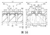
<半導體裝置之製造方法> 利用圖6~圖57,對本實施形態1的半導體裝置之製造方法予以說明。圖6~圖57為,說明本實施形態1之半導體裝置的製程之剖面圖。<Method of Manufacturing Semiconductor Device> The method of manufacturing the semiconductor device of the first embodiment will be described with reference to FIGS. 6 to 57. 6 to 57 are cross-sectional views illustrating the manufacturing process of the semiconductor device of the first embodiment.
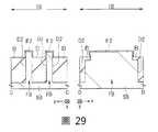
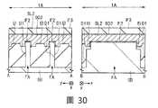
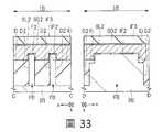
圖6~圖22及圖28~圖56中的偶數圖片編號,為沿著圖1所示之記憶體單元區的A-A線之剖面圖及沿著B-B線之剖面圖。此外,圖7~圖23及圖29~圖57中的奇數圖片編號,為沿著圖2所示之邏輯區的C-C線之剖面圖及沿著D-D線之剖面圖。圖24~圖27為,沿著圖1所示之記憶體單元區的A-A線之剖面圖。The even-numbered picture numbers in FIGS. 6-22 and 28-56 are cross-sectional views taken along the line AA of the memory cell area shown in FIG. 1 and cross-sectional views taken along the line BB of the memory cell area shown in FIG. 1. In addition, the odd-numbered picture numbers in FIGS. 7 to 23 and FIGS. 29 to 57 are cross-sectional views along the CC line of the logic area shown in FIG. 2 and cross-sectional views along the DD line. 24 to 27 are cross-sectional views taken along the line AA of the memory cell area shown in FIG. 1.
首先,如圖6及圖7所示,準備半導體基板SB,於半導體基板SB上,例如利用熱氧化法形成氧化膜PAD。氧化膜PAD,例如由氧化矽構成,其厚度例如為10nm程度。而後,於氧化膜PAD上,例如利用CVD(Chemical Vapor Deposition,化學氣相沉積)法形成絕緣膜IF1。絕緣膜IF1,例如由氮化矽構成,其厚度例如為90nm~120nm程度。而後,於絕緣膜IF1上,例如利用CVD法形成非晶矽膜SL1。非晶矽膜SL1的厚度,例如為160nm程度。First, as shown in FIGS. 6 and 7, a semiconductor substrate SB is prepared, and an oxide film PAD is formed on the semiconductor substrate SB by, for example, a thermal oxidation method. The oxide film PAD is made of, for example, silicon oxide, and its thickness is, for example, about 10 nm. Then, on the oxide film PAD, an insulating film IF1 is formed by, for example, a CVD (Chemical Vapor Deposition) method. The insulating film IF1 is made of, for example, silicon nitride, and its thickness is, for example, about 90 nm to 120 nm. Then, on the insulating film IF1, an amorphous silicon film SL1 is formed by, for example, a CVD method. The thickness of the amorphous silicon film SL1 is, for example, about 160 nm.
接著,如圖8及圖9所示,藉由以光阻圖案為遮罩之乾蝕刻,將非晶矽膜SL1加工。藉此,非晶矽膜SL1,具有俯視時在x方向延伸之長方形形狀。圖8及圖9中,雖於記憶體單元區1A及邏輯區1B分別顯示各1個非晶矽膜SL1的圖案,但包含未圖示之區域,在各個記憶體單元區1A及邏輯區1B,在俯視時行列狀地配置複數之非晶矽膜SL1。記憶體單元區1A之非晶矽膜SL1的Y方向之寬度,較邏輯區1B之非晶矽膜SL1的Y方向之寬度更大。Next, as shown in FIGS. 8 and 9, the amorphous silicon film SL1 is processed by dry etching with the photoresist pattern as a mask. Thereby, the amorphous silicon film SL1 has a rectangular shape extending in the x direction when viewed from above. In FIGS. 8 and 9, although the pattern of one amorphous silicon film SL1 is shown in each of the
接著,如圖10及圖11所示,於非晶矽膜SL1及絕緣膜IF1上,例如利用CVD法沉積氧化矽膜後,將該氧化矽膜回蝕,藉以形成由氧化矽構成之側壁SW1。側壁SW1的Y方向之寬度,例如為20nm~50nm程度。亦即,該回蝕,使非晶矽膜SL1之頂面及絕緣膜IF1之頂面露出。Next, as shown in FIGS. 10 and 11, on the amorphous silicon film SL1 and the insulating film IF1, a silicon oxide film is deposited by, for example, a CVD method, and then the silicon oxide film is etched back to form a sidewall SW1 made of silicon oxide. . The width of the side wall SW1 in the Y direction is, for example, about 20 nm to 50 nm. That is, the etch back exposes the top surface of the amorphous silicon film SL1 and the top surface of the insulating film IF1.
而後,例如藉由濕蝕刻,去除非晶矽膜SL1。藉此,於記憶體單元區1A及邏輯區1B之各自的絕緣膜IF1上,留下覆蓋非晶矽膜SL1之側壁的俯視時呈矩形框狀之側壁SW1。Then, the non-crystalline silicon film SL1 is removed by, for example, wet etching. Thereby, on the insulating film IF1 of each of the
接著,如圖12及圖13所示,藉由以側壁SW1為遮罩之乾蝕刻,將絕緣膜IF1、氧化膜PAD、半導體基板SB之頂面的一部分加工。藉此,在記憶體單元區1A中,形成由包含半導體基板SB之頂面的一部分所構成之鰭FA、及鰭FA周圍之溝槽D1;在邏輯區1B中,形成由包含半導體基板SB之頂面的一部分所構成之鰭FB、及鰭FB周圍之溝槽D2。溝槽D1、D2之各自的深度,例如為120nm~250nm程度。Next, as shown in FIGS. 12 and 13, a part of the top surface of the insulating film IF1, the oxide film PAD, and the semiconductor substrate SB is processed by dry etching with the side wall SW1 as a mask. Thereby, in the
亦即,藉由將從記憶體單元區1A之側壁SW1露出的絕緣膜IF1及半導體基板SB之頂面的一部分加工,而形成於半導體基板SB的頂面中往上方突出之板狀的鰭FA。係半導體基板SB之頂面的一部分之板狀圖案,包含在x方向延伸的2個鰭FA,具有俯視時呈矩形之環狀構造。That is, by processing the insulating film IF1 exposed from the side wall SW1 of the
此外,藉由將從邏輯區1B之側壁SW1露出的絕緣膜IF1及半導體基板SB之頂面的一部分加工,而形成於半導體基板SB的頂面中往上方突出之板狀的鰭FB。係半導體基板SB之頂面的一部分之板狀圖案,包含在x方向延伸的2個鰭FB,具有俯視時呈矩形之環狀構造。In addition, the insulating film IF1 exposed from the side wall SW1 of the
接著,如圖14及圖15所示,例如利用CVD法,以絕緣膜嵌入溝槽D1、D2之各自的內側。該絕緣膜,例如由氧化矽構成。之後,例如利用CMP(Chemical Mechanical Polishing,化學機械研磨)法研磨該絕緣膜及側壁SW1。藉此,使記憶體單元區1A及邏輯區1B的絕緣膜IF1之頂面露出,將絕緣膜IF1之頂面,以及分別嵌入至溝槽D1、D2的該絕緣膜之頂面平坦化。藉由該研磨,去除側壁SW1。嵌入至各個溝槽D1、D2之該絕緣膜,構成元件隔離區EI。Next, as shown in FIGS. 14 and 15, for example, using the CVD method, an insulating film is embedded inside each of the trenches D1 and D2. The insulating film is made of silicon oxide, for example. After that, the insulating film and the sidewall SW1 are polished by, for example, a CMP (Chemical Mechanical Polishing) method. Thereby, the top surface of the insulating film IF1 of the
接著,如圖16及圖17所示,藉由以光阻圖案為遮罩之乾蝕刻,將從元件隔離區EI之頂面露出的絕緣膜IF1之一部分、及包含半導體基板SB之頂面的板狀圖案之一部分去除。Next, as shown in FIGS. 16 and 17, by dry etching with a photoresist pattern as a mask, a part of the insulating film IF1 exposed from the top surface of the element isolation region EI, and a portion of the insulating film IF1 including the top surface of the semiconductor substrate SB Part of the plate pattern is removed.
亦即,於記憶體單元區1A中,將具有矩形之環狀構造的板狀圖案中之例如在y方向延伸的部分加工,亦即,將連接在y方向排列的2個鰭FA彼此之端部的部分加工。藉此,將構成板狀圖案,在y方向延伸之圖案中的上部之一部分去除。在此步驟中同樣地,於邏輯區1B中,將具有矩形之環狀構造的板狀圖案中之例如在y方向延伸的部分加工,亦即,將連接在y方向排列的2個鰭FB彼此之端部的部分加工。藉此,將構成板狀圖案,在y方向延伸之圖案中的上部之一部分去除。That is, in the
藉此,形成將在y方向彼此相鄰的鰭FA之彼此的端部連接之下部圖案UP。同樣地,形成將在y方向彼此相鄰的鰭FB之彼此的端部連接之下部圖案UP。去除之圖案為任意圖案,藉由此一去除步驟,分別形成最後構成電路所用之任意的鰭FA、FB。Thereby, the lower part pattern UP connecting the ends of the fins FA adjacent to each other in the y direction is formed. Similarly, the lower part pattern UP is formed to connect the ends of the fins FB adjacent to each other in the y direction. The pattern to be removed is an arbitrary pattern, and through this removal step, arbitrary fins FA and FB used to form the final circuit are respectively formed.
而後,在該步驟中去除絕緣膜IF1之一部分及板狀圖案之一部分的區域,利用CVD法等,例如嵌入由氧化矽構成之絕緣膜。之後,例如利用CMP法施行研磨,藉此,使該絕緣膜之頂面平坦化,露出絕緣膜IF1之頂面。Then, in this step, a part of the insulating film IF1 and a part of the plate-like pattern are removed, and an insulating film made of silicon oxide is embedded by a CVD method or the like, for example. After that, polishing is performed by, for example, a CMP method, thereby flattening the top surface of the insulating film, and exposing the top surface of the insulating film IF1.
另,圖16及圖17中,將該絕緣膜,與在利用圖14及圖15說明的步驟中嵌入至溝槽D1、D2之各自的內側之絕緣膜的邊界,以點線表示。此等絕緣膜,構成元件隔離區EI。In addition, in FIGS. 16 and 17, the boundary between the insulating film and the insulating film embedded in the inner side of each of the trenches D1 and D2 in the steps described with reference to FIGS. 14 and 15 is indicated by a dotted line. These insulating films constitute the element isolation region EI.
接著,如圖18及圖19所示,形成露出邏輯區1B,覆蓋記憶體單元區1A的光阻圖案RP後,藉由以回蝕使邏輯區1B的元件隔離區EI之頂面後退,而從元件隔離區EI露出絕緣膜IF1之側壁。該回蝕,可利用濕蝕刻或乾蝕刻之任一方式。Next, as shown in FIGS. 18 and 19, after forming the photoresist pattern RP exposing the
接著,如圖20及圖21所示,藉由濕蝕刻,去除絕緣膜IF1而露出鰭FA、FB之各自的頂面上之氧化膜PAD。此處,記憶體單元區1A之鰭FA的Y方向之寬度,例如為20nm~50nm程度;元件隔離區EI的Y方向之寬度,例如為90nm。此外,記憶體單元區1A的從鰭FA之頂面突出的元件隔離區EI之高度,例如為50nm~70nm程度。另一方面,邏輯區1B的從鰭FB之頂面突出的元件隔離區EI之高度,例如為10nm~20nm程度。Next, as shown in FIGS. 20 and 21, the insulating film IF1 is removed by wet etching to expose the oxide film PAD on the top surface of each of the fins FA and FB. Here, the width in the Y direction of the fin FA of the
接著,如圖22及圖23所示,藉由利用等向性乾蝕刻使元件隔離區EI之頂面後退,而將氧化膜PAD去除,從元件隔離區EI露出鰭FA、FB之各自的側壁。此時,係板狀圖案之一部分的在y方向延伸之下部圖案UP,並未從元件隔離區EI露出。亦即,從元件隔離區EI之頂面露出的半導體基板SB,僅為在x方向延伸的鰭FA及鰭FB。Next, as shown in FIGS. 22 and 23, the top surface of the element isolation region EI is retreated by isotropic dry etching, and the oxide film PAD is removed, and the respective sidewalls of the fins FA and FB are exposed from the element isolation region EI . At this time, the lower pattern UP of a part of the plate-shaped pattern extending in the y direction is not exposed from the element isolation region EI. That is, the semiconductor substrate SB exposed from the top surface of the element isolation region EI is only the fin FA and the fin FB extending in the x direction.
此外,記憶體單元區1A中,藉由利用等向性乾蝕刻使元件隔離區EI之頂面後退,而使元件隔離區EI之頂面在沿著y方向的剖面中成為凸形。此係因,記憶體單元區1A中,蝕刻從露出的元件隔離區EI之頂面方向及側面方向進行之故。然則,若元件隔離區EI之頂面的凸部之高度過高,則元件隔離區EI之頂面的段差變大,形成元件隔離區EI後之加工處理變得困難,故元件隔離區EI之頂面的凸部之高度,例如宜為20nm~30nm程度。此外,從元件隔離區EI之頂面露出的鰭FA的高度,例如為40nm~60nm程度。In addition, in the
另一方面,邏輯區1B中,元件隔離區EI之頂面並未成為凸形,而呈幾近平坦。亦即,邏輯區1B的元件隔離區EI之頂面的平面度,較記憶體單元區1A的元件隔離區EI之頂面的平面度成為更小。On the other hand, in the
此係因,在施行等向性乾蝕刻之前,從鰭FB之頂面突出的元件隔離區EI之高度較從鰭FA之頂面突出的元件隔離區EI之高度更低,且在y方向彼此相鄰的鰭FB之間隔較在y方向彼此相鄰的鰭FA之間隔更小,故邏輯區1B中,蝕刻主要從元件隔離區EI之頂面方向進行。This is because before the isotropic dry etching is performed, the height of the element isolation region EI protruding from the top surface of the fin FB is lower than the height of the element isolation region EI protruding from the top surface of the fin FA, and each other in the y direction The interval between adjacent fins FB is smaller than the interval between adjacent fins FA in the y direction. Therefore, in the
然則,若在y方向彼此相鄰的鰭FB之間隔變大,則邏輯區1B中,元件隔離區EI之頂面在沿著y方向的剖面中亦成為凸形。However, if the interval between the fins FB adjacent to each other in the y direction becomes larger, the top surface of the element isolation region EI in the
另,對於元件隔離區EI之頂面的等向性乾蝕刻,亦可對各個記憶體單元區1A及邏輯區1B分別施行。此一情況,未施行蝕刻之區域係在覆蓋光阻圖案的狀態下施行蝕刻。如此地,在記憶體單元區1A中使元件隔離區EI之頂面呈凸形,在邏輯區1B中使元件隔離區EI之頂面呈平坦形狀亦可。In addition, the isotropic dry etching of the top surface of the element isolation region EI can also be performed on each
本實施形態1之主要特徵的1個為,藉由使記憶體單元區1A的元件隔離區EI之頂面呈凸形,而使記憶體單元區1A中在y方向彼此相鄰的記憶體單元之間的捕集性絕緣膜之路徑變長,抑制電荷擴散的影響。One of the main features of the first embodiment is that by making the top surface of the element isolation region EI of the
作為調節凸部的高度及寬度之方法,例如具有下述方法。As a method of adjusting the height and width of the convex portion, for example, there is the following method.
(1)藉由改變絕緣膜IF1的厚度,而可改變凸部的高度。(1) By changing the thickness of the insulating film IF1, the height of the convex portion can be changed.
(2)在利用等向性乾蝕刻使元件隔離區EI的頂面後退之前,藉由使記憶體單元區1A之元件隔離區EI的頂面均一地後退,而可改變凸部的高度。例如在利用圖14說明的步驟之後,利用濕蝕刻使元件隔離區EI的頂面後退。(2) Before retreating the top surface of the device isolation region EI by isotropic dry etching, the height of the convex portion can be changed by uniformly retreating the top surface of the device isolation region EI of the
(3)藉由改變氧化膜PAD的厚度,而可改變凸部的寬度。例如氧化膜PAD為厚膜之情況,等向性乾蝕刻的起點,離半導體基板SB之頂面變遠,至獲得其望的鰭FA之高度為止的蝕刻時間變長。此一結果,凸部的寬度變窄。(3) By changing the thickness of the oxide film PAD, the width of the convex portion can be changed. For example, when the oxide film PAD is a thick film, the starting point of the isotropic dry etching becomes farther from the top surface of the semiconductor substrate SB, and the etching time until the desired height of the fin FA becomes longer. As a result, the width of the convex portion becomes narrow.
(4)藉由改變絕緣膜IF的構造,而可改變凸部的寬度。(4) By changing the structure of the insulating film IF, the width of the convex portion can be changed.
作為一例,利用圖24~圖27,於以下內容,說明關於使絕緣膜IF1為由下層之氮化矽膜SN1、氧化矽膜SO1、及上層之氮化矽膜SN2所構成的疊層構造之情況。As an example, using FIGS. 24 to 27, in the following description, the insulating film IF1 is a laminated structure composed of a lower silicon nitride film SN1, a silicon oxide film SO1, and an upper silicon nitride film SN2. Happening.
將元件隔離區EI之頂面加工使其平坦後(圖24),去除上層之氮化矽膜SN2(圖25),進一步,利用等向性乾蝕刻使元件隔離區EI之頂面及側面後退(圖26)。此時,將氧化矽膜SO1去除。而後,去除下層之氮化矽膜SN1(圖27)。藉此,可形成於較鰭FA之頂面更為上方具有寬度d的元件隔離區EI,該寬度d較在y方向彼此相鄰的鰭FA之間的距離c更小。此處,利用等向性乾蝕刻使元件隔離區EI之頂面後退,露出鰭FA,藉而可將凸部的寬度減小。After processing the top surface of the element isolation region EI to make it flat (Figure 24), remove the upper silicon nitride film SN2 (Figure 25), and further, use isotropic dry etching to retreat the top and side surfaces of the element isolation region EI (Figure 26). At this time, the silicon oxide film SO1 is removed. Then, the lower silicon nitride film SN1 is removed (FIG. 27). Thereby, an element isolation region EI having a width d above the top surface of the fin FA can be formed, and the width d is smaller than the distance c between the fins FA adjacent to each other in the y direction. Here, isotropic dry etching is used to retreat the top surface of the element isolation region EI to expose the fin FA, thereby reducing the width of the convex portion.
接著,如圖28及圖29所示,形成絕緣膜IF2,其覆蓋從元件隔離區EI之頂面露出的鰭FA、FB之各自的表面。絕緣膜IF2,例如可利用熱氧化法形成,例如由氧化矽構成。絕緣膜IF2覆蓋鰭FA、FB之各自的頂面及側壁,元件隔離區EI之頂面從絕緣膜IF2露出。絕緣膜IF2的厚度,例如為1nm~2nm程度。Next, as shown in FIGS. 28 and 29, an insulating film IF2 is formed to cover the respective surfaces of the fins FA and FB exposed from the top surface of the element isolation region EI. The insulating film IF2 can be formed by, for example, a thermal oxidation method, and is made of silicon oxide, for example. The insulating film IF2 covers the respective top surfaces and sidewalls of the fins FA and FB, and the top surface of the element isolation region EI is exposed from the insulating film IF2. The thickness of the insulating film IF2 is, for example, about 1 nm to 2 nm.
接著,如圖30及圖31所示,於元件隔離區EI及絕緣膜IF2上,例如利用CVD法形成多晶矽膜SL2後,將多晶矽膜SL2之頂面藉由CMP法等研磨。從鰭FA、FB之各自的頂面至多晶矽膜SL2的頂面為止之多晶矽膜SL2的厚度,例如為60nm~150nm程度。Next, as shown in FIGS. 30 and 31, on the element isolation region EI and the insulating film IF2, after forming the polysilicon film SL2 by, for example, the CVD method, the top surface of the polysilicon film SL2 is polished by the CMP method or the like. The thickness of the polysilicon film SL2 from the top surface of each of the fins FA and FB to the top surface of the polysilicon film SL2 is, for example, about 60 nm to 150 nm.
而後,藉由將多晶矽膜SL2之頂面熱氧化,而形成覆蓋該頂面的氧化矽膜SO2。氧化矽膜SO2的厚度,例如為6nm~10nm程度。而後,於氧化矽膜SO2上,例如利用CVD法形成絕緣膜IF3。絕緣膜IF3,例如由氮化矽構成,其厚度例如為90nm程度。Then, by thermally oxidizing the top surface of the polysilicon film SL2, a silicon oxide film SO2 covering the top surface is formed. The thickness of the silicon oxide film SO2 is, for example, about 6 nm to 10 nm. Then, on the silicon oxide film SO2, an insulating film IF3 is formed by, for example, a CVD method. The insulating film IF3 is made of, for example, silicon nitride, and its thickness is, for example, about 90 nm.
接著,如圖32及圖33所示,藉由以光阻圖案為遮罩之乾蝕刻,將記憶體單元區1A之絕緣膜IF3、氧化矽膜SO2、多晶矽膜SL2及絕緣膜IF2加工。亦即,在以光阻圖案(未圖示)覆蓋邏輯區1B之狀態下施行圖案化。光阻圖案,在該圖案化後去除。藉此,鰭FA的正上方中,在x方向排列形成由絕緣膜IF3、氧化矽膜SO2、多晶矽膜SL2及絕緣膜IF2所構成之疊層圖案。藉由此一圖案化,形成由多晶矽膜SL2構成之控制閘極電極CG,並形成由絕緣膜IF2構成之閘極絕緣膜GF。Next, as shown in FIGS. 32 and 33, the insulating film IF3, the silicon oxide film SO2, the polysilicon film SL2, and the insulating film IF2 of the
由絕緣膜IF3及控制閘極電極CG所構成之疊層圖案,在y方向延伸,配置為橫跨複數之鰭FA上及閘極絕緣膜GF上。記憶體單元區1A中,在該疊層圖案形成處以外的區域,以上述蝕刻將記憶體單元區1A之絕緣膜IF3、氧化矽膜SO2、多晶矽膜SL2及絕緣膜IF2去除,藉而露出鰭FA之表面及元件隔離區EI之頂面。The laminated pattern composed of the insulating film IF3 and the control gate electrode CG extends in the y direction and is arranged to straddle the plurality of fins FA and the gate insulating film GF. In the
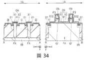
接著,如圖34及圖35所示,利用熱氧化法,將從閘極絕緣膜GF露出的鰭FA之頂面及側壁與控制閘極電極CG之側壁氧化。藉此,形成覆蓋鰭FA之頂面及側壁與控制閘極電極CG之側壁的氧化矽膜(底部氧化膜)X1。圖34,雖顯示從鰭FA之頂面至控制閘極電極CG的側壁連續形成之氧化矽膜X1,但亦可未在閘極絕緣膜GF的側壁形成氧化矽膜X1。Next, as shown in FIGS. 34 and 35, the top surface and sidewalls of the fin FA exposed from the gate insulating film GF and the sidewalls of the control gate electrode CG are oxidized by a thermal oxidation method. Thereby, a silicon oxide film (bottom oxide film) X1 covering the top surface and sidewalls of the fin FA and the sidewalls of the control gate electrode CG is formed. Although FIG. 34 shows the silicon oxide film X1 continuously formed from the top surface of the fin FA to the sidewall of the control gate electrode CG, the silicon oxide film X1 may not be formed on the sidewall of the gate insulating film GF.
而後,例如利用CVD法,於氧化矽膜X1、絕緣膜IF3及元件隔離區EI上方形成氮化矽膜N1。該氮化矽膜N1,在之後形成的記憶體單元中作為貯存電荷所用之捕集性絕緣膜而作用。另,此處,雖對於形成氮化矽膜N1作為捕集性絕緣膜予以說明,但作為捕集性絕緣膜並不限於氮化矽膜N1,例如亦可形成由矽酸鉿(HfSiO)構成之絕緣膜。而後,例如利用CVD法而於氮化矽膜N1上形成氧化矽膜(頂部氧化膜)X2。Then, a silicon nitride film N1 is formed on the silicon oxide film X1, the insulating film IF3, and the element isolation region EI by using, for example, the CVD method. The silicon nitride film N1 functions as a trapping insulating film for storing charges in the memory cell to be formed later. In addition, here, although the formation of the silicon nitride film N1 as a trapping insulating film is described, the trapping insulating film is not limited to the silicon nitride film N1. For example, it may be formed of hafnium silicate (HfSiO). The insulating film. Then, a silicon oxide film (top oxide film) X2 is formed on the silicon nitride film N1 by, for example, a CVD method.
從半導體基板SB側依序疊層有氧化矽膜X1、氮化矽膜N1及氧化矽膜X2而構成的疊層膜,構成ONO膜ON。與控制閘極電極CG的側壁接觸之ONO膜ON,由從控制閘極電極CG側起依序在x方向形成之氧化矽膜X1、氮化矽膜N1及氧化矽膜X2構成。此處,ONO膜ON之最上層的頂部氧化膜之材料,不限於氧化矽,例如亦可為氧化鋁(Al2O3)。A laminated film composed of a silicon oxide film X1, a silicon nitride film N1, and a silicon oxide film X2 are sequentially stacked from the side of the semiconductor substrate SB to form an ONO film ON. The ONO film ON that is in contact with the sidewall of the control gate electrode CG is composed of a silicon oxide film X1, a silicon nitride film N1, and a silicon oxide film X2 formed in the x direction sequentially from the control gate electrode CG side. Here, the material of the top oxide film of the uppermost layer of the ONO film ON is not limited to silicon oxide, and may also be aluminum oxide (Al2 O3 ), for example.
另,ONO膜ON,原則上,係指由氧化矽膜X1、氮化矽膜N1及氧化矽膜X2構成之疊層膜,但為了說明的方便,亦有將由氮化矽膜N1及氧化矽膜X2構成之疊層膜稱作ONO膜ON的情況。In addition, the ONO film ON, in principle, refers to a laminated film composed of a silicon oxide film X1, a silicon nitride film N1, and a silicon oxide film X2. However, for the convenience of description, it may also be composed of a silicon nitride film N1 and a silicon oxide film. The laminated film formed by the film X2 is called the ONO film ON.
接著,如圖36及圖37所示,於ONO膜ON上,例如利用CVD法形成多晶矽膜SL3。多晶矽膜SL3的厚度,至少具有控制閘極電極CG的厚度以上之大小。此處,以較由控制閘極電極CG、氧化矽膜SO2及絕緣膜IF3構成之疊層膜的膜厚更大之膜厚,形成多晶矽膜SL3,藉而覆蓋包含控制閘極電極CG、氧化矽膜SO2、絕緣膜IF3及ONO膜ON的疊層膜。之後,利用CMP法等將多晶矽膜SL3之頂面平坦化。Next, as shown in FIGS. 36 and 37, a polysilicon film SL3 is formed on the ONO film ON by, for example, the CVD method. The thickness of the polysilicon film SL3 has at least a size greater than the thickness of the control gate electrode CG. Here, a polysilicon film SL3 is formed with a film thickness greater than that of the laminated film composed of the control gate electrode CG, the silicon oxide film SO2 and the insulating film IF3, thereby covering the control gate electrode CG, the oxide film A laminated film of silicon film SO2, insulating film IF3, and ONO film ON. After that, the top surface of the polysilicon film SL3 is planarized by the CMP method or the like.
而後,藉由施行回蝕,而使多晶矽膜SL3之頂面後退,例如使多晶矽膜SL3之頂面的高度,與控制閘極電極CG之頂面的高度一致。藉此,使絕緣膜IF3及覆蓋絕緣膜IF3的ONO膜ON,在多晶矽膜SL3之頂面上突出。藉由上述對於多晶矽膜SL3之平坦化步驟及回蝕步驟,將邏輯區1B之多晶矽膜SL3去除。Then, by performing etch back, the top surface of the polysilicon film SL3 is retreated, for example, the height of the top surface of the polysilicon film SL3 is made the same as the height of the top surface of the control gate electrode CG. Thereby, the insulating film IF3 and the ONO film covering the insulating film IF3 are turned ON to protrude on the top surface of the polysilicon film SL3. The polysilicon film SL3 in the
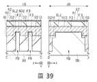
接著,如圖38及圖39所示,於ONO膜ON及多晶矽膜SL3上方,例如利用CVD法形成絕緣膜。該絕緣膜,例如由氮化矽構成,其厚度例如為10~50nm。而後,藉由乾蝕刻,從該絕緣膜,露出多晶矽膜SL3之頂面、及絕緣膜IF3之正上方的ONO膜ON之頂面。藉此,於絕緣膜IF3的側壁,隔著ONO膜ON,形成由該絕緣膜構成之側壁SW2。藉由該乾蝕刻步驟,去除邏輯區1B之該絕緣膜。Next, as shown in FIGS. 38 and 39, an insulating film is formed on the ONO film ON and the polysilicon film SL3 by, for example, the CVD method. The insulating film is made of, for example, silicon nitride, and its thickness is, for example, 10 to 50 nm. Then, by dry etching, the top surface of the polysilicon film SL3 and the top surface of the ONO film ON directly above the insulating film IF3 are exposed from the insulating film. Thereby, on the side wall of the insulating film IF3, the side wall SW2 made of the insulating film is formed with the ONO film ON interposed therebetween. Through the dry etching step, the insulating film of the
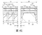
接著,如圖40及圖41所示,藉由以側壁SW2為硬罩之乾蝕刻,將多晶矽膜SL3加工。藉此,從多晶矽膜SL3,露出與鰭FA之頂面及側壁接觸的ONO膜ON之頂面。於控制閘極電極CG旁邊之兩側,隔著ONO膜ON而形成由多晶矽膜SL3的圖案構成之記憶體閘極電極MG。然則,與控制閘極電極CG之一方的側壁鄰接之記憶體閘極電極MG,係在之後的步驟去除之圖案,並未留在完成後之半導體裝置。Next, as shown in FIGS. 40 and 41, the polysilicon film SL3 is processed by dry etching with the side wall SW2 as a hard mask. Thereby, from the polysilicon film SL3, the top surface of the ONO film ON that is in contact with the top surface and sidewalls of the fin FA is exposed. On both sides of the control gate electrode CG, a memory gate electrode MG composed of a pattern of a polysilicon film SL3 is formed with the ONO film ON interposed therebetween. However, the memory gate electrode MG adjacent to one of the sidewalls of the control gate electrode CG is a pattern removed in a subsequent step and is not left in the completed semiconductor device.
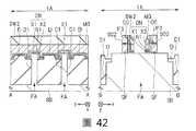
接著,如圖42及圖43所示,藉由以光阻圖案為遮罩之乾蝕刻,將與由控制閘極電極CG及絕緣膜IF3構成的疊層膜之一方的側壁鄰接之記憶體閘極電極MG、及該記憶體閘極電極MG正上方之側壁SW2去除。藉此,留下與控制閘極電極CG之另一方的側壁鄰接之記憶體閘極電極MG。而後,將從控制閘極電極CG、記憶體閘極電極MG露出的ONO膜ON去除。Next, as shown in FIGS. 42 and 43, by dry etching with the photoresist pattern as a mask, the memory gate adjacent to one of the sidewalls of the laminated film composed of the control gate electrode CG and the insulating film IF3 The electrode MG and the side wall SW2 directly above the memory gate electrode MG are removed. This leaves the memory gate electrode MG adjacent to the other side wall of the control gate electrode CG. Then, the ONO film ON exposed from the control gate electrode CG and the memory gate electrode MG is removed.
亦即,ONO膜ON,僅留在記憶體閘極電極MG與鰭FA之間、記憶體閘極電極MG與控制閘極電極CG之間、及側壁SW2與絕緣膜IF3之間。因此,記憶體單元區1A,在從控制閘極電極CG及記憶體閘極電極MG露出的區域中,露出鰭FA之頂面及側壁、與元件隔離區EI之頂面。此外,在記憶體單元區1A中露出絕緣膜IF3的頂面及一方的側壁,在邏輯區1B中露出絕緣膜IF3的頂面。That is, the ONO film ON remains only between the memory gate electrode MG and the fin FA, between the memory gate electrode MG and the control gate electrode CG, and between the sidewall SW2 and the insulating film IF3. Therefore, in the
沿著鰭FA的頂面延伸,亦即沿著半導體基板SB延伸之ONO膜ON,與沿著控制閘極電極CG的側壁延伸之ONO膜ON係連續形成,具有L字形的剖面。於鰭FA上,將具有控制閘極電極CG、及沿著ONO膜ON而與該控制閘極電極CG鄰接之記憶體閘極電極MG的圖案形成一對,在一對控制閘極電極CG彼此之間,一對記憶體閘極電極MG彼此相對向。而後,以在之後對鰭FA施行的雜質注入步驟中防止鰭FA受到損害等為目的,而對鰭FA之頂面及側壁施行氧化處理亦可。The ONO film ON extending along the top surface of the fin FA, that is, along the semiconductor substrate SB, is formed continuously with the ONO film ON extending along the sidewall of the control gate electrode CG, and has an L-shaped cross section. On the fin FA, a pattern having a control gate electrode CG and a memory gate electrode MG adjacent to the control gate electrode CG along the ONO film ON is formed as a pair, and the pair of control gate electrodes CG are connected to each other. In between, a pair of memory gate electrodes MG face each other. Then, for the purpose of preventing damage to the fin FA in the impurity implantation step performed on the fin FA later, it is also possible to perform oxidation treatment on the top surface and the sidewalls of the fin FA.
接著,如圖44及圖45所示,形成覆蓋記憶體單元區1A,露出邏輯區1B之一部分的光阻圖案(未圖示)後,藉由以該光阻圖案為遮罩之乾蝕刻,將邏輯區1B之絕緣膜IF3、氧化矽膜SO2、多晶矽膜SL2及絕緣膜IF2加工。藉此,於鰭FB之正上方,將以絕緣膜IF2、由多晶矽膜SL2構成之虛擬閘極電極DG、氧化矽膜SO2、及絕緣膜IF3構成之疊層膜,在x方向排列而形成一對。在此等疊層膜旁邊的區域,露出鰭FB及元件隔離區EI之頂面。亦即,於鰭FB上,隔著絕緣膜IF2而形成虛擬閘極電極DG、氧化矽膜SO2、及絕緣膜IF3。虛擬閘極電極DG,係在之後的步驟中去除之虛擬閘極電極,並未留在完成的半導體裝置。Then, as shown in FIGS. 44 and 45, after forming a photoresist pattern (not shown) covering the
而後,將該光阻圖案去除後,施行以絕緣膜IF3及側壁SW2為遮罩的離子注入步驟,藉而將n型雜質(例如磷(P)或砷(As))植入鰭FA、FB之各自的頂面。藉此,形成複數之係雜質濃度較低的n型半導體區之延伸區EX。記憶體單元區1A之延伸區EX,形成於具有控制閘極電極CG、及隔著ONO膜ON而與該控制閘極電極CG鄰接之記憶體閘極電極MG的圖案旁邊之鰭FA的頂面。邏輯區1B之延伸區EX,形成於虛擬閘極電極DG旁邊之鰭FB的頂面。此處,因應必要,亦可分別對各個鰭FA、FB施行p型雜質(例如硼(B))的植入以作為環形注入。Then, after the photoresist pattern is removed, an ion implantation step using the insulating film IF3 and the sidewall SW2 as a mask is performed, thereby implanting n-type impurities (such as phosphorus (P) or arsenic (As)) into the fins FA and FB The top surface of each. Thereby, a plurality of extension regions EX of the n-type semiconductor region with a relatively low impurity concentration are formed. The extension area EX of the
接著,如圖46及圖47所示,於半導體基板SB上,例如利用CVD法形成絕緣膜。該絕緣膜,例如由氧化矽、氮化矽或其等之疊層膜構成。而後,藉由乾蝕刻,從該絕緣膜露出各個鰭FA、FB及絕緣膜IF3之頂面。藉此,記憶體單元區1A中,在包含控制閘極電極CG、記憶體閘極電極MG、ONO膜ON、氧化矽膜SO2、絕緣膜IF3及側壁SW2的圖案之兩側的側壁,形成由該絕緣膜構成的側壁SW3。此外,邏輯區1B中,在由虛擬閘極電極DG、氧化矽膜SO2及絕緣膜IF3構成的疊層膜之兩側的側壁,形成由該絕緣膜構成的側壁SW3。Next, as shown in FIGS. 46 and 47, an insulating film is formed on the semiconductor substrate SB by, for example, the CVD method. The insulating film is made of, for example, silicon oxide, silicon nitride, or a laminated film thereof. Then, by dry etching, the top surfaces of the respective fins FA, FB and the insulating film IF3 are exposed from the insulating film. Thereby, in the
而後,藉由施行將絕緣膜IF3及側壁SW2、SW3分別作為遮罩的離子注入步驟,而將n型雜質(例如磷(P)或砷(As))植入鰭FA、FB之各自的頂面。藉此,形成複數之係雜質濃度較高的n型半導體區之擴散層DF。記憶體單元區1A的擴散層DF,形成於具有控制閘極電極CG、及隔著ONO膜ON而與該控制閘極電極CG鄰接之記憶體閘極電極MG的圖案旁邊之鰭FA的頂面。邏輯區1B的擴散層DF,形成於虛擬閘極電極DG旁邊之鰭FB的頂面。Then, by performing an ion implantation step that uses the insulating film IF3 and the sidewalls SW2 and SW3 as masks, respectively, n-type impurities (such as phosphorus (P) or arsenic (As)) are implanted into the tops of the fins FA and FB. surface. Thereby, a plurality of diffusion layers DF of the n-type semiconductor region with a relatively high impurity concentration are formed. The diffusion layer DF of the
擴散層DF,相較在與該擴散層DF接觸之延伸區EX,在x方向中形成於離控制閘極電極CG、記憶體閘極電極MG或虛擬閘極電極DG更遠的位置。擴散層DF,形成深度較延伸區EX更淺,n型雜質濃度更高。彼此接觸之延伸區EX及擴散層DF,構成電晶體的源極/汲極區。而後,為了使延伸區EX內及擴散層DF內之雜質活性化,因應必要而施行熱處理。The diffusion layer DF is formed at a position farther from the control gate electrode CG, the memory gate electrode MG, or the dummy gate electrode DG in the x direction than in the extension region EX contacting the diffusion layer DF. The formation depth of the diffusion layer DF is shallower than that of the extension region EX, and the concentration of n-type impurities is higher. The extension area EX and the diffusion layer DF that are in contact with each other constitute the source/drain area of the transistor. Then, in order to activate the impurities in the extension region EX and the diffusion layer DF, heat treatment is performed as necessary.
另,此處,雖對以同一步驟形成記憶體單元區1A及邏輯區1B之各自的源極/汲極區進行說明,但吾人考慮在形成有相較於形成於邏輯區1B之電晶體為高耐受電壓的記憶體單元之記憶體單元區1A中,使源極/汲極區之雜質濃度,較邏輯區1B的源極/汲極區之雜質濃度更高。因此,亦可將記憶體單元區1A之延伸區EX及擴散層DF的形成步驟、與邏輯區1B之延伸區EX及擴散層DF的形成步驟分別施行。此外,此處,雖對藉由離子注入形成源極/汲極區之方法進行說明,但亦可取代施行離子注入,而利用磊晶成長法,將導入有雜質的磊晶層,形成於各閘極電極旁邊的鰭FA、FB之各自的頂面及側壁。In addition, although the source/drain regions of the
接著,如圖48及圖49所示,於半導體基板SB上,例如利用CVD法,依序形成例如具有5nm~20nm的膜厚之由氮化矽構成的絕緣膜(未圖示)、及例如由氧化矽構成的層間絕緣膜IL。層間絕緣膜IL,至少具有較控制閘極電極CG更大的膜厚,此處,具有較由閘極絕緣膜GF、控制閘極電極CG、氧化矽膜SO2及絕緣膜IF3構成之疊層膜更厚的膜厚。Next, as shown in FIG. 48 and FIG. 49, on the semiconductor substrate SB, for example, an insulating film (not shown) made of silicon nitride having a film thickness of 5 nm to 20 nm is sequentially formed by, for example, the CVD method, and Interlayer insulating film IL made of silicon oxide. The interlayer insulating film IL has at least a larger film thickness than the control gate electrode CG. Here, it has a layered film composed of a gate insulating film GF, a control gate electrode CG, a silicon oxide film SO2, and an insulating film IF3. Thicker film thickness.
接著,如圖50及圖51所示,將層間絕緣膜IL之頂面,例如利用CMP法研磨,藉而使其平坦化。該研磨步驟,將絕緣膜IF3及側壁SW2全部去除,將側壁SW3及ONO膜ON之各自的上部之一部分去除,使控制閘極電極CG、記憶體閘極電極MG及虛擬閘極電極DG之各自的頂面露出。亦即,使控制閘極電極CG、記憶體閘極電極MG及虛擬閘極電極DG,與ONO膜ON、側壁SW3及層間絕緣膜IL之各自的頂面,在大致相同的平面中平坦化,於相同高度一致。Next, as shown in FIG. 50 and FIG. 51, the top surface of the interlayer insulating film IL is polished by, for example, a CMP method to planarize it. In this polishing step, the insulating film IF3 and the side wall SW2 are all removed, and a part of the upper part of each of the side wall SW3 and the ONO film ON is removed, so that each of the control gate electrode CG, the memory gate electrode MG, and the dummy gate electrode DG The top surface is exposed. That is, the top surfaces of the control gate electrode CG, the memory gate electrode MG, and the dummy gate electrode DG, and the respective top surfaces of the ONO film ON, the sidewall SW3, and the interlayer insulating film IL are flattened in substantially the same plane, Consistent at the same height.
藉此,頂面露出的控制閘極電極CG及記憶體閘極電極MG、以及由形成於包含控制閘極電極CG及記憶體閘極電極MG的圖案之兩側的延伸區EX及擴散層DF構成之源極/汲極區,構成分離閘極式的記憶體單元MC。亦即,記憶體單元MC,構成MONOS型之非揮發性記憶體,其具有包含控制閘極電極CG之第1電晶體、及包含記憶體閘極電極MG之第2電晶體。Thereby, the control gate electrode CG and the memory gate electrode MG exposed on the top surface, and the extension area EX and the diffusion layer DF formed on both sides of the pattern including the control gate electrode CG and the memory gate electrode MG The constituted source/drain region constitutes a separate gate type memory cell MC. That is, the memory cell MC constitutes a non-volatile memory of the MONOS type, and has a first transistor including the control gate electrode CG and a second transistor including the memory gate electrode MG.
如圖50所示,記憶體單元區1A之控制閘極電極CG,在鰭FA及元件隔離區EI之各自的正上方中,以橫跨複數之鰭FA的上部之方式在y方向延伸。此外,控制閘極電極CG,形成為嵌入從元件隔離區EI突出的複數之鰭FA彼此之間。此外,如圖51所示,邏輯區1B之虛擬閘極電極DG,於鰭FB及元件隔離區EI之各自的正上方中,以橫跨複數之鰭FB的上部之方式在y方向延伸。此外,虛擬閘極電極DG,形成為嵌入從元件隔離區EI突出的複數之鰭FB彼此之間。As shown in FIG. 50, the control gate electrode CG of the
接著,如圖52及圖53所示,在以光阻圖案(未圖示)保護記憶體單元區1A之控制閘極電極CG及記憶體閘極電極MG的狀態下,藉由濕蝕刻,去除虛擬閘極電極DG。而後,去除絕緣膜IF2。另,亦可不去除絕緣膜IF2,而在之後的步驟將其作為形成於邏輯區1B的閘極絕緣膜GI之一部分使用。藉由該去除步驟,邏輯區1B中,在去除虛擬閘極電極DG及絕緣膜IF2的區域形成溝槽。之後,將記憶體單元區1A的該光阻圖案去除。Next, as shown in FIGS. 52 and 53, in a state where the control gate electrode CG and the memory gate electrode MG of the
接著,如圖54及圖55所示,於半導體基板SB上,例如利用ALD(Atomiclayer Deposition:原子層沉積)法形成絕緣膜後,於該絕緣膜上,例如利用濺鍍法形成金屬膜,藉而將由該絕緣膜及該金屬膜構成之疊層膜嵌入該溝槽內。之後,例如利用CMP法施行研磨,藉而將層間絕緣膜IL上之多餘的該絕緣膜及金屬膜去除,使層間絕緣膜IL、控制閘極電極CG及記憶體閘極電極MG之各自的頂面露出。藉此,形成嵌入至該溝槽內的由絕緣膜構成之閘極絕緣膜GI、及隔著閘極絕緣膜GI而嵌入至該溝槽內的由金屬膜構成之閘極電極G1。Next, as shown in FIGS. 54 and 55, an insulating film is formed on the semiconductor substrate SB by, for example, ALD (Atomic Layer Deposition) method, and then a metal film is formed on the insulating film by, for example, sputtering. The laminated film composed of the insulating film and the metal film is embedded in the trench. After that, polishing is performed by, for example, the CMP method, thereby removing the excess insulating film and metal film on the interlayer insulating film IL, so that the top of each of the interlayer insulating film IL, the control gate electrode CG, and the memory gate electrode MG is removed. Face exposed. Thereby, a gate insulating film GI made of an insulating film embedded in the trench, and a gate electrode G1 made of a metal film embedded in the trench via the gate insulating film GI are formed.
閘極電極G1、及形成於閘極電極G1旁邊的鰭FB之一對源極/汲極區,構成電晶體Q1。電晶體Q1,係以相較於第1電晶體、第2電晶體皆更低的電壓驅動之低耐受電壓的MISFET,具有金屬閘極電極。構成閘極絕緣膜GI之絕緣膜,例如,可使用二氧化鉿(HfO2)膜、二氧化鋯(ZrO2)膜、氧化鋁(Al2O3)膜、氧化鉭(Ta2O5)膜或氧化鑭(La2O3)膜等金屬氧化物膜。亦即,閘極絕緣膜GI,為介電常數較氧化矽膜更高的high-k膜(高介電常數膜)。The gate electrode G1 and a pair of source/drain regions of the fin FB formed beside the gate electrode G1 constitute a transistor Q1. Transistor Q1 is a low withstand voltage MISFET driven at a lower voltage than the first and second transistors, and has a metal gate electrode. The insulating film constituting the gate insulating film GI, for example, a hafnium dioxide (HfO2 ) film, a zirconium dioxide (ZrO2 ) film, an aluminum oxide (Al2 O3 ) film, or a tantalum oxide (Ta2 O5 ) film can be used A metal oxide film such as a film or a lanthanum oxide (La2 O3) film. That is, the gate insulating film GI is a high-k film (high dielectric constant film) having a higher dielectric constant than a silicon oxide film.
構成閘極電極G1之該金屬膜,例如係以2層疊層膜構成。該疊層膜,具有從半導體基板SB側起依序疊層的第1金屬膜及第2金屬膜。第1金屬膜,例如由鈦鋁(TiAl)膜構成;第2金屬膜,例如由鋁(Al)構成。此外,亦可於第1金屬膜及第2金屬膜之間,夾設鈦(Ti)膜、氮化鈦(TiN)膜或其等之疊層膜,調整電晶體Q1的閾值電壓。另,圖55中將該第1金屬膜及第2金屬膜顯示為1層金屬膜。The metal film constituting the gate electrode G1 is composed of, for example, a two-layer laminated film. This laminated film has a first metal film and a second metal film laminated in this order from the side of the semiconductor substrate SB. The first metal film is made of, for example, a titanium aluminum (TiAl) film; the second metal film is made of, for example, aluminum (Al). In addition, a titanium (Ti) film, a titanium nitride (TiN) film, or a laminated film thereof may be interposed between the first metal film and the second metal film to adjust the threshold voltage of the transistor Q1. In addition, in FIG. 55, the first metal film and the second metal film are shown as a single metal film.
閘極絕緣膜GI,在該溝槽內之中,覆蓋閘極電極G1之底面及側壁、與該溝槽之底面及側壁。另,利用圖52及圖53說明的步驟中在將絕緣膜IF2去除之情況,藉由在形成閘極絕緣膜GI前施行氧化處理,而於該溝槽之底面形成新的絕緣膜,將該絕緣膜作為閘極絕緣膜GI之一部分使用亦可。此外,此處,雖對在去除虛擬閘極電極DG後形成high-k膜進行說明,但亦可在構成虛擬閘極電極DG之多晶矽膜SL2(參考圖31)的形成之前,在利用圖23說明的步驟之後,形成high-k膜,將該high-k膜留下作為邏輯區1B的閘極絕緣膜GI。The gate insulating film GI covers the bottom surface and sidewalls of the gate electrode G1 and the bottom surface and sidewalls of the trench in the trench. In addition, when the insulating film IF2 is removed in the steps described in FIGS. 52 and 53, an oxidation treatment is performed before the gate insulating film GI is formed, and a new insulating film is formed on the bottom surface of the trench. The insulating film may be used as a part of the gate insulating film GI. In addition, here, although the formation of the high-k film after removing the dummy gate electrode DG is described, it is also possible to use FIG. 23 before the formation of the polysilicon film SL2 (refer to FIG. 31) constituting the dummy gate electrode DG. After the described steps, a high-k film is formed, and the high-k film is left as the gate insulating film GI of the
接著,如圖56及圖57所示,藉由絕緣膜IF4覆蓋邏輯區1B的閘極電極G1之頂面後,形成覆蓋控制閘極電極CG及記憶體閘極電極MG之各自的頂面之矽化物層SI。Next, as shown in FIGS. 56 and 57, the top surface of the gate electrode G1 of the
絕緣膜IF4,例如係由藉由CVD法形成之氧化矽構成。此處,以覆蓋記憶體單元區1A及邏輯區1B的方式形成絕緣膜IF4後,藉由施行圖案化而將記憶體單元區1A之絕緣膜IF4去除。藉此,留下覆蓋邏輯區1B的層間絕緣膜IL、側壁SW3及閘極電極G1之各自的頂面之絕緣膜IF4。The insulating film IF4 is made of, for example, silicon oxide formed by the CVD method. Here, after the insulating film IF4 is formed to cover the
而後,在露出的控制閘極電極CG及記憶體閘極電極MG上方,例如利用濺鍍法形成由鎳(Ni)或鈷(Co)構成的金屬膜後,施行熱處理,使該金屬膜,與控制閘極電極CG及記憶體閘極電極MG之各自的頂面反應。Then, over the exposed control gate electrode CG and memory gate electrode MG, a metal film made of nickel (Ni) or cobalt (Co) is formed by, for example, sputtering, and then heat treatment is performed to make the metal film and Control the respective top surface reactions of the gate electrode CG and the memory gate electrode MG.
藉此,形成矽化物層SI,其覆蓋控制閘極電極CG及記憶體閘極電極MG之各自的頂面,由鎳矽化物(NiSi)或鈷矽化物(CoSi)構成。Thereby, a silicide layer SI is formed, which covers the top surfaces of the control gate electrode CG and the memory gate electrode MG, and is composed of nickel silicide (NiSi) or cobalt silicide (CoSi).
而後,將未反應的金屬膜藉由濕蝕刻等去除。藉此,露出層間絕緣膜IL及絕緣膜IF4。此處,藉由絕緣膜IF4覆蓋閘極電極G1,故可防止係金屬閘極電極之閘極電極G1因該濕蝕刻而被去除。此外,在閘極電極G1上並未形成矽化物層SI。Then, the unreacted metal film is removed by wet etching or the like. Thereby, the interlayer insulating film IL and the insulating film IF4 are exposed. Here, by covering the gate electrode G1 with the insulating film IF4, it is possible to prevent the gate electrode G1, which is a metal gate electrode, from being removed by the wet etching. In addition, the silicide layer SI is not formed on the gate electrode G1.
而後,雖未圖示,但於層間絕緣膜IL上進一步形成層間絕緣膜,並形成貫通此等層間絕緣膜,而與控制閘極電極CG、記憶體閘極電極MG、源極/汲極區或閘極電極G1連接的複數之接觸栓塞(連接部),藉而完成本實施形態1之半導體裝置。Then, although not shown, an interlayer insulating film is further formed on the interlayer insulating film IL, and the interlayer insulating film is formed to penetrate through the interlayer insulating film, and is connected to the control gate electrode CG, the memory gate electrode MG, and the source/drain region. Or a plurality of contact plugs (connecting portions) connected to the gate electrode G1, thereby completing the semiconductor device of the first embodiment.
具體而言,例如利用CVD法於層間絕緣膜IL上形成由氧化矽等構成之層間絕緣膜後,藉由以光阻圖案為遮罩之乾蝕刻,形成貫通由層間絕緣膜IL及其上方之該層間絕緣膜所構成的疊層層間絕緣膜之複數之接觸孔。接觸孔,係使構成記憶體單元MC的源極/汲極區之擴散層DF、構成電晶體Q1的源極/汲極區之擴散層DF、控制閘極電極CG、記憶體閘極電極MG或閘極電極G1之各自的頂面,從疊層層間絕緣膜露出之開口部。另,於控制閘極電極CG及記憶體閘極電極MG之各自的正上方之接觸孔的底面,露出矽化物層SI之頂面。Specifically, for example, after forming an interlayer insulating film made of silicon oxide or the like on the interlayer insulating film IL by a CVD method, dry etching with a photoresist pattern as a mask is used to form the interlayer insulating film IL and the upper portion of the interlayer insulating film. The plurality of contact holes of the laminated interlayer insulating film formed by the interlayer insulating film. The contact hole is formed by the diffusion layer DF constituting the source/drain region of the memory cell MC, the diffusion layer DF constituting the source/drain region of the transistor Q1, the control gate electrode CG, and the memory gate electrode MG Or the respective top surfaces of the gate electrode G1 are exposed from the openings of the interlayer insulating film. In addition, the bottom surface of the contact hole directly above each of the control gate electrode CG and the memory gate electrode MG exposes the top surface of the silicide layer SI.
而後,例如利用濺鍍法等在疊層層間絕緣膜上,作為連接用的導電膜,例如形成主要由鎢(W)構成之金屬膜,藉此將金屬膜完全嵌入各接觸孔內。此處,例如形成由鈦(Ti)、氮化鈦(TiN)或其等之疊層膜所構成的阻障導體膜後,於阻障導體膜上形成由鎢(W)膜構成的主要導體膜,藉而形成由阻障導體膜及主要導體膜構成的該金屬膜。Then, a metal film mainly composed of tungsten (W) is formed as a conductive film for connection on the interlayer insulating film by, for example, sputtering, etc., thereby completely embedding the metal film in each contact hole. Here, for example, after forming a barrier conductor film composed of titanium (Ti), titanium nitride (TiN) or a laminated film thereof, a main conductor composed of a tungsten (W) film is formed on the barrier conductor film Film, thereby forming the metal film composed of the barrier conductor film and the main conductor film.
之後,藉由將疊層層間絕緣膜上之不需要的該金屬膜以CMP法等去除,而形成嵌入至各接觸孔內之接觸栓塞。接觸栓塞,與控制閘極電極CG、記憶體閘極電極MG、源極/汲極區或閘極電極G1電性連接。After that, the unnecessary metal film on the laminated interlayer insulating film is removed by a CMP method or the like to form a contact plug embedded in each contact hole. The contact plug is electrically connected to the control gate electrode CG, the memory gate electrode MG, the source/drain region or the gate electrode G1.
如此地,依照本實施形態1,則藉由使記憶體單元區1A的元件隔離區EI之頂面呈凸形,而在彼此相鄰的記憶體單元MC之間,捕集性絕緣膜之路徑變長,故可抑制電荷擴散的影響,改善半導體裝置的可靠度。In this way, according to the first embodiment, by making the top surface of the element isolation region EI of the
<變形例> 利用圖58及圖59,對本實施形態1的變形例之半導體裝置予以說明。圖58為,顯示本實施形態1之半導體裝置的記憶體單元區之沿著圖1的A-A線之放大剖面圖。圖59為,顯示本實施形態1的變形例之半導體裝置的記憶體單元區之沿著圖1的A-A線之放大剖面圖。<Modifications> The semiconductor device according to the modification of the first embodiment will be described with reference to FIGS. 58 and 59. FIG. 58 is an enlarged cross-sectional view along the line AA of FIG. 1 showing the memory cell region of the semiconductor device of the first embodiment. FIG. 59 is an enlarged cross-sectional view along the line AA of FIG. 1 showing the memory cell region of the semiconductor device according to a modification of the first embodiment.
前述實施形態1,如圖3所示,形成於彼此相鄰的鰭FA之間的元件隔離區EI之頂面的凸部,例如形成於2個鰭FA之間的幾近中央部,且係遠離2個鰭FA之各自的側壁之位置。因此,如圖58所示,在彼此相鄰的鰭FA之間,ONO膜ON之頂面,成為仿照元件隔離區EI之頂面的形狀。此外,位於和鰭FA的側壁隔著ONO膜ON之位置的記憶體閘極電極MG之下部的端部(圖58以箭頭H表示的區域),較元件隔離區EI之凸部的最高位置位於更下方。In the foregoing
然則,本實施形態1之變形例,如圖59所示,彼此相鄰的鰭FA之間的元件隔離區EI之頂面呈凸形,但ONO膜ON嵌入至鰭FA與元件隔離區EI的凸部之間。因此,在彼此相鄰的鰭FA之間,ONO膜ON之頂面成為幾近平坦。此外,位於和鰭FA的側壁隔著ONO膜ON之位置的記憶體閘極電極MG之下部的端部(圖59以箭頭H表示的區域),較元件隔離區EI之凸部的最高位置位於更上方。However, in the modification of the first embodiment, as shown in FIG. 59, the top surface of the element isolation region EI between the adjacent fins FA is convex, but the ONO film ON is embedded in the fin FA and the element isolation region EI. Between the convex parts. Therefore, between the fins FA adjacent to each other, the top surface of the ONO film ON becomes almost flat. In addition, the lower end of the memory gate electrode MG (the area indicated by arrow H in FIG. 59) located at the position where the ONO film ON is separated from the sidewall of the fin FA is located higher than the highest position of the convex part of the element isolation region EI More above.
如同前述,作為施行記憶體單元之「寫入」及「抹除」的操作法,分別可應用SSI方式之寫入及FN方式之抹除。SSI方式之寫入中,電場及熱電子的注入位置集中在鰭FA之上部(圖58及圖59以箭頭E表示的區域)。此外,FN方式之抹除中,電場及電洞的注入位置集中在記憶體閘極電極MG之下部的端部(圖58及圖59以箭頭H表示的區域)。As mentioned above, as the operation method of "writing" and "erase" of the memory cell, the SSI method of writing and the FN method of erasing can be applied respectively. In SSI writing, the electric field and hot electron injection positions are concentrated on the upper part of the fin FA (the area indicated by the arrow E in FIGS. 58 and 59). In addition, in the erasing of the FN method, the electric field and hole injection positions are concentrated at the end of the lower part of the memory gate electrode MG (the area indicated by the arrow H in FIGS. 58 and 59).
然則,如同變形例,藉由使鰭FA與元件隔離區EI之凸部的距離接近,以ONO膜ON填埋兩者間,而使記憶體閘極電極MG之下部的端部接近鰭FA之上部。藉此,改寫的不匹配(mismatch)得到改善,故除了可抑制在元件隔離區EI之頂面形成凸部所造成的資料變動以外,可追求改寫效率的改善。However, as in the modified example, by making the distance between the fin FA and the convex part of the element isolation region EI close, the ONO film ON fills the gap between the two, so that the end of the lower part of the memory gate electrode MG is close to the fin FA. Upper part. As a result, the rewriting mismatch is improved, so in addition to suppressing the data change caused by the formation of the convex portion on the top surface of the element isolation region EI, the improvement of rewriting efficiency can be pursued.
(實施形態2) <半導體裝置的構造> 利用圖60及圖61,對本實施形態2之半導體裝置的構造予以說明。圖60為,顯示本實施形態2之半導體裝置的記憶體單元區之俯視圖。圖61為,顯示本實施形態2之半導體裝置的記憶體單元區之沿著圖60的E-E線及F-F線之剖面圖。(Embodiment 2) <Structure of semiconductor device> The structure of the semiconductor device of the second embodiment will be described with reference to FIGS. 60 and 61. FIG. 60 is a plan view showing the memory cell area of the semiconductor device of the second embodiment. FIG. 61 is a cross-sectional view showing the memory cell region of the semiconductor device of the second embodiment along the EE line and the FF line in FIG. 60. FIG.
圖61的沿著E-E線之剖面,顯示沿著記憶體單元區的鰭上方之閘極電極的延伸方向之剖面;沿著F-F線之剖面,顯示沿著記憶體單元區之鰭的延伸方向之剖面。另,圖60中,省略源極/汲極區、層間絕緣膜、各閘極電極上之矽化物層等的圖示。The cross section along the line E-E of FIG. 61 shows the cross section along the extending direction of the gate electrode above the fin of the memory cell area; the cross section along the FF line shows the fin along the memory cell area The section of the extension direction. In addition, in FIG. 60, the illustration of the source/drain regions, the interlayer insulating film, the silicide layer on each gate electrode, etc. is omitted.
本實施形態2之半導體裝置,與前述實施形態1之半導體裝置相異的點,在於記憶體單元區1A的元件隔離區EI之頂面的形狀。亦即,前述實施形態1之半導體裝置中,記憶體單元區1A的元件隔離區EI之頂面為凸形,但本實施形態2之半導體裝置中,記憶體單元區1A的元件隔離區EI之頂面為凹形。記憶體單元區1A的元件隔離區EI之頂面的形狀以外的構造,與前述實施形態1之半導體裝置幾近相同,故下述內容,以與前述實施形態1相異的點為中心而予以說明。The semiconductor device of the second embodiment is different from the semiconductor device of the aforementioned first embodiment in the shape of the top surface of the element isolation region EI of the
如圖60及圖61所示,記憶體單元區1A中,記憶體單元MC,形成於板狀的鰭FA之上部,該板狀的鰭FA為半導體基板SB之一部分,形成於半導體基板SB之上部。於複數之鰭FA彼此之間形成溝槽D1,該溝槽D1形成於半導體基板SB之頂面。As shown in FIGS. 60 and 61, in the
元件隔離區EI,係嵌入至溝槽D1之絕緣膜。然則,元件隔離區EI並未完全嵌入溝槽D1,鰭FA之各自的一部分在元件隔離區EI之頂面上突出。從元件隔離區EI之頂面露出的鰭FA的高度,例如為40nm~60nm程度。元件隔離區EI,例如由氧化矽構成。The element isolation region EI is an insulating film embedded in the trench D1. However, the element isolation region EI is not completely embedded in the trench D1, and a part of each of the fins FA protrudes on the top surface of the element isolation region EI. The height of the fin FA exposed from the top surface of the element isolation region EI is, for example, about 40 nm to 60 nm. The element isolation region EI is made of silicon oxide, for example.
如圖61所示,元件隔離區EI之頂面在沿著y方向的剖面中成為凹形。換而言之,則於在y方向彼此相鄰的鰭FA之間,元件隔離區EI之頂面的一部分或全部位於較連結面更低的位置,該連結面,將與一方的鰭FA之側壁接觸的元件隔離區EI之頂面的位置、和與另一方的鰭FA之側壁接觸的元件隔離區EI之頂面的位置連結。As shown in FIG. 61, the top surface of the element isolation region EI becomes a concave shape in the cross section along the y direction. In other words, between the fins FA adjacent to each other in the y-direction, part or all of the top surface of the element isolation region EI is located at a lower position than the connecting surface, and the connecting surface will be in contact with one of the fins FA The position of the top surface of the element isolation region EI that is in contact with the sidewall is connected to the position of the top surface of the element isolation region EI that is in contact with the sidewall of the other fin FA.
然則,若元件隔離區EI之頂面的凹部之深度過大,則元件隔離區EI之頂面的段差變大,形成元件隔離區EI後之加工處理變得困難。因此,元件隔離區EI之頂面的凹部的深度,例如宜為40nm~80nm程度,例如若使在y方向彼此相鄰的鰭FA之間隔為e,使凹部之深度為f,則f/e宜為0.4~0.8程度。此處,凹部之深度,係於在y方向相鄰的鰭FA之間,從連結面至元件隔離區EI之頂面的最低位置之距離,而該連結面,將與一方的鰭FA之側壁接觸的元件隔離區EI之頂面的位置、和與另一方的鰭FA之側壁接觸的元件隔離區EI之頂面的位置連結。However, if the depth of the recess on the top surface of the element isolation region EI is too large, the step difference of the top surface of the element isolation region EI becomes larger, and the processing after the formation of the element isolation region EI becomes difficult. Therefore, the depth of the recess on the top surface of the element isolation region EI is preferably about 40 nm to 80 nm, for example, if the distance between the fins FA adjacent to each other in the y direction is e, and the depth of the recess is f, then f/e It is preferably about 0.4 to 0.8. Here, the depth of the recess is the distance between the adjacent fins FA in the y-direction from the connection surface to the lowest position of the top surface of the element isolation region EI, and the connection surface will be the same as the sidewall of one fin FA The position of the top surface of the element isolation region EI that is in contact is connected to the position of the top surface of the element isolation region EI that is in contact with the sidewall of the other fin FA.
如此地,藉由使記憶體單元區1A的元件隔離區EI之頂面為凹形,相較於元件隔離區EI之頂面為平坦形狀的情況,在y方向彼此相鄰的記憶體單元MC間之中,捕集性絕緣膜之路徑變長,故可抑制電荷擴散的影響。In this way, by making the top surface of the device isolation region EI of the
另,本實施形態2中,雖省略其說明,但邏輯區的元件隔離區EI之頂面並未成為凹形,而成為幾近平坦。亦即,邏輯區的元件隔離區EI之頂面的平面度,較記憶體單元區1A的元件隔離區EI之頂面的平面度成為更小。In addition, although the description is omitted in the second embodiment, the top surface of the element isolation region EI of the logic region is not concave, but almost flat. That is, the flatness of the top surface of the device isolation region EI of the logic region is smaller than the flatness of the top surface of the device isolation region EI of the
進一步,記憶體單元區1A中,於在y方向排列之複數之鰭FA的正上方,以橫跨此等鰭FA之方式,形成有在y方向延伸的控制閘極電極CG、及在y方向延伸的記憶體閘極電極MG。Furthermore, in the
控制閘極電極CG,隔著閘極絕緣膜GF而形成於從元件隔離區EI之頂面露出的鰭FA之頂面及側壁。閘極絕緣膜GF,例如由氧化矽構成;控制閘極電極CG,例如由多晶矽構成。The control gate electrode CG is formed on the top surface and sidewalls of the fin FA exposed from the top surface of the element isolation region EI via the gate insulating film GF. The gate insulating film GF is made of, for example, silicon oxide; the control gate electrode CG is made of, for example, polysilicon.
x方向的控制閘極電極CG之一方的側壁由側壁SW3覆蓋,於另一方的側壁,隔著ONO膜ON而形成記憶體閘極電極MG。此外,記憶體閘極電極MG,隔著ONO膜ON而形成於從元件隔離區EI之頂面露出的鰭FA之頂面及側壁。亦即,ONO膜ON,具有沿著鰭FA的頂面、控制閘極電極CG的側壁而連續形成之L字形的剖面。記憶體閘極電極MG,藉由ONO膜ON,而與控制閘極電極CG及鰭FA絕緣。One side wall of the control gate electrode CG in the x direction is covered by the side wall SW3, and on the other side wall, the memory gate electrode MG is formed with the ONO film ON interposed therebetween. In addition, the memory gate electrode MG is formed on the top surface and sidewalls of the fin FA exposed from the top surface of the element isolation region EI via the ONO film ON. That is, the ONO film ON has a zigzag cross-section formed continuously along the top surface of the fin FA and the sidewall of the control gate electrode CG. The memory gate electrode MG is insulated from the control gate electrode CG and the fin FA by the ONO film ON.
<半導體裝置之特徵及效果> 本實施形態2之半導體裝置的主要特徵,在於使記憶體單元區1A的元件隔離區EI之頂面為凹形的點。<Characteristics and Effects of Semiconductor Device> The main feature of the semiconductor device of the second embodiment is that the top surface of the element isolation region EI of the
本實施形態2之半導體裝置,藉由使記憶體單元區1A的元件隔離區EI之頂面呈凹形,而將在y方向彼此相鄰的記憶體單元MC之間的氮化矽膜N1(捕集性絕緣膜)之路徑增長。亦即,形成有凹部的情況,相較於未形成凹部的情況,氮化矽膜N1之路徑變長,電荷之擴散距離變長,故可抑制經由在y方向彼此相鄰的記憶體單元MC之間的氮化矽膜N1之路徑的資料變動。藉此,可改善半導體裝置的可靠度。In the semiconductor device of the second embodiment, by making the top surface of the element isolation region EI of the
<半導體裝置之製造方法> 利用圖62~圖67,對本實施形態2的半導體裝置(記憶體單元區)之製造方法予以說明。圖62~圖67為說明本實施形態2之半導體裝置(記憶體單元區)的製程之剖面圖,係沿著圖60的E-E線之剖面圖。<Method of Manufacturing Semiconductor Device> The method of manufacturing the semiconductor device (memory cell region) of the second embodiment will be described with reference to FIGS. 62 to 67. 62 to 67 are cross-sectional views illustrating the manufacturing process of the semiconductor device (memory cell region) of the second embodiment, and are cross-sectional views taken along the line E-E of FIG. 60.
首先,如圖62所示,在記憶體單元區1A中,形成由包含半導體基板SB之頂面的一部分所構成之鰭FA、及鰭FA周圍之溝槽D1。溝槽D1的深度,例如為120nm~250nm程度。First, as shown in FIG. 62, in the
另,至形成溝槽D1為止的製造過程,與前述實施形態1幾近相同(參考圖6~圖12),故省略其說明。In addition, the manufacturing process up to the formation of the trench D1 is almost the same as that of the aforementioned first embodiment (refer to FIGS. 6 to 12), so the description thereof is omitted.
接著,如圖63所示,於溝槽D1之底面及側壁,例如利用熱氧化法形成氧化膜SO3。氧化膜SO3,例如由氧化矽構成,其厚度例如為10nm~20nm程度。Next, as shown in FIG. 63, an oxide film SO3 is formed on the bottom surface and sidewalls of the trench D1, for example, by a thermal oxidation method. The oxide film SO3 is made of, for example, silicon oxide, and its thickness is, for example, about 10 nm to 20 nm.
接著,如圖64所示,例如利用CVD法,以絕緣膜IF5嵌入溝槽D1的內側。絕緣膜IF5,例如由氧化矽構成。之後,例如利用CMP法研磨絕緣膜IF5。藉此,使絕緣膜IF1之頂面露出,將絕緣膜IF1之頂面、與嵌入至溝槽D1的絕緣膜IF5之頂面平坦化。氧化膜SO3、及嵌入至溝槽D1的絕緣膜IF5,構成元件隔離區EI。Next, as shown in FIG. 64, the insulating film IF5 is embedded inside the trench D1 by, for example, the CVD method. The insulating film IF5 is made of silicon oxide, for example. After that, the insulating film IF5 is polished by, for example, a CMP method. Thereby, the top surface of the insulating film IF1 is exposed, and the top surface of the insulating film IF1 and the top surface of the insulating film IF5 embedded in the trench D1 are flattened. The oxide film SO3 and the insulating film IF5 embedded in the trench D1 constitute an element isolation region EI.
接著,如圖65所示,藉由以回蝕使絕緣膜IF5之頂面後退,而從元件隔離區EI露出絕緣膜IF1之側壁。該回蝕,可利用濕蝕刻或乾蝕刻之任一方式。Next, as shown in FIG. 65, the top surface of the insulating film IF5 is retreated by etchback, and the sidewall of the insulating film IF1 is exposed from the element isolation region EI. The etch back can be either wet etching or dry etching.
接著,如圖66所示,藉由濕蝕刻去除絕緣膜IF1,使鰭FA之頂面的氧化膜PAD露出。此處,記憶體單元區1A之鰭FA的Y方向之寬度,例如為20nm~50nm程度;元件隔離區EI的Y方向之寬度,例如為90nm。Next, as shown in FIG. 66, the insulating film IF1 is removed by wet etching to expose the oxide film PAD on the top surface of the fin FA. Here, the width in the Y direction of the fin FA of the
接著,如圖67所示,利用濕蝕刻去除氧化膜PAD,使元件隔離區EI之頂面後退,藉而從元件隔離區EI露出鰭FA之側壁。Next, as shown in FIG. 67, the oxide film PAD is removed by wet etching, and the top surface of the element isolation region EI is receded, thereby exposing the sidewall of the fin FA from the element isolation region EI.
利用熱氧化法形成之氧化膜SO3的蝕刻率,較利用CVD法形成之絕緣膜IF5的蝕刻率緩慢,故絕緣膜IF5之濕蝕刻較氧化膜SO3進行更快。藉此,元件隔離區EI之頂面在沿著y方向的剖面中成為凹形。然則,若元件隔離區EI之頂面的凹部之深度過大,則元件隔離區EI之頂面的段差變大,形成元件隔離區EI後之加工處理變得困難,故元件隔離區EI之頂面的凹部的深度,例如宜為40nm~80nm程度。此外,從元件隔離區EI之頂面露出的鰭FA的高度,例如為40nm~60nm程度。The etching rate of the oxide film SO3 formed by the thermal oxidation method is slower than the etching rate of the insulating film IF5 formed by the CVD method, so the wet etching of the insulating film IF5 is performed faster than the oxide film SO3. Thereby, the top surface of the element isolation region EI becomes a concave shape in the cross section along the y direction. However, if the depth of the recess on the top surface of the element isolation region EI is too large, the step difference of the top surface of the element isolation region EI becomes larger, and the processing after the formation of the element isolation region EI becomes difficult, so the top surface of the element isolation region EI The depth of the concave portion is preferably about 40 nm to 80 nm, for example. In addition, the height of the fin FA exposed from the top surface of the element isolation region EI is, for example, about 40 nm to 60 nm.
本實施形態2之主要特徵的1個為,藉由使記憶體單元區1A的元件隔離區EI之頂面呈凹形,而使記憶體單元區1A中在y方向彼此相鄰的記憶體單元之間的捕集性絕緣膜之路徑變長,抑制電荷擴散的影響。One of the main features of the second embodiment is that by making the top surface of the element isolation region EI of the
之後,與前述實施形態1同樣地,形成控制閘極電極CG、閘極絕緣膜GF、記憶體閘極電極MG、ONO膜ON、源極/汲極區、矽化物層SI等,藉而大致完成半導體裝置。After that, in the same manner as in the foregoing first embodiment, the control gate electrode CG, the gate insulating film GF, the memory gate electrode MG, the ONO film ON, the source/drain regions, the silicide layer SI, etc. are formed, thereby substantially Complete the semiconductor device.
如此地,依照本實施形態2,則藉由使記憶體單元區1A的元件隔離區EI之頂面為凹形,而在彼此相鄰的記憶體單元MC之間,捕集性絕緣膜之路徑變長,故可抑制電荷擴散的影響,改善半導體裝置的可靠度。In this way, according to the second embodiment, by making the top surface of the element isolation region EI of the
以上,雖依據實施形態具體地說明本案發明人所提出的發明,但本發明並未限定於上述實施形態,自然可在不脫離其要旨之範圍內進行各種變更。As mentioned above, although the invention proposed by the inventor of the present application has been specifically described based on the embodiment, the invention is not limited to the above-mentioned embodiment, and various modifications can be made without departing from the gist of the invention.
本發明至少包含以下實施形態。The present invention includes at least the following embodiments.
[附註1] 一種半導體裝置之製造方法,包含如下步驟: (a)步驟,於半導體基板之主面上,形成第1絕緣膜; (b)步驟,將該第1絕緣膜及該半導體基板依序加工,形成複數之溝槽,藉而形成由該半導體基板之一部分構成的複數之突出部,該複數之突出部,在沿著該半導體基板之該主面的第1方向延伸,且在沿著該半導體基板之該主面而與該第1方向直交的第2方向彼此分隔; (c)步驟,利用熱氧化法,在該複數之溝槽的內部之露出的該半導體基板之表面形成第1氧化膜; (d)步驟,利用CVD法,以第2氧化膜嵌入該複數之溝槽的內部; (e)步驟,將該第1絕緣膜之頂面及該第2氧化膜之頂面平坦化; (f)步驟,使該第2氧化膜後退,露出該第1絕緣膜之側壁; (g)步驟,去除該第1絕緣膜; (h)步驟,利用濕蝕刻,使該第1及第2氧化膜之頂面後退,露出複數之該突出部之側壁; (i)步驟,形成第1閘極電極,其和從該第1及第2氧化膜之頂面露出的該突出部之上部的頂面及側壁隔著第2絕緣膜,在該第2方向延伸;以及 (j)步驟,形成第2閘極電極,其和從該第1及第2氧化膜之頂面露出的該突出部之上部的頂面及側壁與該第1閘極電極的一方之側壁,隔著包含捕集性絕緣膜的第3絕緣膜,在該第2方向延伸; 於在該第2方向彼此相鄰的該突出部之間,該第2氧化膜之頂面較第1面更低,該第1面,將與一方的該突出部之側壁接觸的該第1氧化膜之頂面的位置、和與另一方的該突出部之側壁接觸的該第1氧化膜之頂面的位置連結。[Note 1] A method of manufacturing a semiconductor device, including the following steps: (a) step, forming a first insulating film on the main surface of a semiconductor substrate; (b) step, following the first insulating film and the semiconductor substrate Sequential processing to form a plurality of grooves, thereby forming a plurality of protrusions constituted by a part of the semiconductor substrate, the plurality of protrusions extend in the first direction along the main surface of the semiconductor substrate, and are in the first direction along the main surface of the semiconductor substrate. A second direction perpendicular to the first direction is separated from each other along the main surface of the semiconductor substrate; (c) step, using a thermal oxidation method, to form a first surface on the exposed semiconductor substrate inside the plurality of trenches 1 oxide film; (d) step, using a CVD method to embed a second oxide film inside the plurality of trenches; (e) step, the top surface of the first insulating film and the top surface of the second oxide film Planarization; (f) step, retreat the second oxide film to expose the sidewall of the first insulating film; (g) step, remove the first insulating film; (h) step, use wet etching to make the first insulating film And the top surface of the second oxide film retreats, exposing the side walls of a plurality of the protrusions; (i) step, forming a first gate electrode, and the protrusions exposed from the top surfaces of the first and second oxide films The top surface and sidewalls of the upper portion extend in the second direction with the second insulating film interposed therebetween; and (j) step is to form a second gate electrode which is exposed from the top surface of the first and second oxide films The top surface and the side wall of the upper portion of the protruding portion and the side wall of one side of the first gate electrode extend in the second direction via a third insulating film including a trapping insulating film; and to each other in the second direction Between the adjacent protrusions, the top surface of the second oxide film is lower than the first surface, and the first surface is the position of the top surface of the first oxide film that will be in contact with the side wall of the protrusion , Is connected to the position of the top surface of the first oxide film that is in contact with the side wall of the other protruding portion.
[附註2] 附註1記載之半導體裝置之製造方法中, 若使該第1面的該第2方向之寬度為W,使從該第1面至該第2氧化膜之頂面的最低位置之距離為D,則D/W為0.4~0.8。[Note 2] In the semiconductor device manufacturing method described in
[附註3] 附註1記載之半導體裝置之製造方法中, 從該第1面至該第2氧化膜之頂面的最低位置之距離,為40nm~60nm。[Note 3] In the semiconductor device manufacturing method described in
1A‧‧‧記憶體單元區1B‧‧‧邏輯區CG‧‧‧控制閘極電極D1、D2‧‧‧溝槽DF‧‧‧擴散層DG‧‧‧虛擬閘極電極EI‧‧‧元件隔離區EX‧‧‧延伸區FA、FB‧‧‧鰭G1‧‧‧閘極電極GF、GI‧‧‧閘極絕緣膜IF1、IF2、IF3、IF4、IF5‧‧‧絕緣膜IL‧‧‧層間絕緣膜MC‧‧‧記憶體單元MG‧‧‧記憶體閘極電極N1‧‧‧氮化矽膜ON‧‧‧ONO膜PAD‧‧‧氧化膜Q1‧‧‧電晶體RP‧‧‧光阻圖案SI‧‧‧矽化物層SB‧‧‧半導體基板SL1‧‧‧非晶矽膜SL2、SL3‧‧‧多晶矽膜SN1、SN2‧‧‧氮化矽膜SO1、SO2‧‧‧氧化矽膜SO3‧‧‧氧化膜SW1、SW2、SW3‧‧‧側壁UP‧‧‧下部圖案X1、X2‧‧‧氧化矽膜1A‧‧‧
圖1係顯示實施形態1之半導體裝置的記憶體單元區之俯視圖。 圖2係顯示實施形態1之半導體裝置的邏輯區之俯視圖。 圖3係顯示實施形態1之半導體裝置的記憶體單元區之沿著圖1的A-A線及B-B線之剖面圖。 圖4係顯示實施形態1之半導體裝置的邏輯區之沿著圖2的C-C線及D-D線之剖面圖。 圖5係實施形態1之半導體裝置的形成於記憶體單元區之記憶體單元的鳥瞰圖。 圖6係說明實施形態1之半導體裝置(記憶體單元區)的製程之沿著圖1的A-A線及B-B線之剖面圖。 圖7係說明實施形態1之半導體裝置(邏輯區)的製程之沿著圖2的C-C線及D-D線之剖面圖。 圖8係說明接續圖6之半導體裝置的製程之剖面圖。 圖9係說明接續圖7之半導體裝置的製程之剖面圖。 圖10係說明接續圖8之半導體裝置的製程之剖面圖。 圖11係說明接續圖9之半導體裝置的製程之剖面圖。 圖12係說明接續圖10之半導體裝置的製程之剖面圖。 圖13係說明接續圖11之半導體裝置的製程之剖面圖。 圖14係說明接續圖12之半導體裝置的製程之剖面圖。 圖15係說明接續圖13之半導體裝置的製程之剖面圖。 圖16係說明接續圖14之半導體裝置的製程之剖面圖。 圖17係說明接續圖15之半導體裝置的製程之剖面圖。 圖18係說明接續圖16之半導體裝置的製程之剖面圖。 圖19係說明接續圖17之半導體裝置的製程之剖面圖。 圖20係說明接續圖18之半導體裝置的製程之剖面圖。 圖21係說明接續圖19之半導體裝置的製程之剖面圖。 圖22係說明接續圖20之半導體裝置的製程之剖面圖。 圖23係說明接續圖21之半導體裝置的製程之剖面圖。 圖24係顯示實施形態1之半導體裝置的記憶體單元區之沿著圖1的A-A線之剖面圖。 圖25係顯示實施形態1之半導體裝置的記憶體單元區之沿著圖1的A-A線之剖面圖。 圖26係顯示實施形態1之半導體裝置的記憶體單元區之沿著圖1的A-A線之剖面圖。 圖27係顯示實施形態1之半導體裝置的記憶體單元區之沿著圖1的A-A線之剖面圖。 圖28係說明接續圖22之半導體裝置的製程之剖面圖。 圖29係說明接續圖23之半導體裝置的製程之剖面圖。 圖30係說明接續圖28之半導體裝置的製程之剖面圖。 圖31係說明接續圖29之半導體裝置的製程之剖面圖。 圖32係說明接續圖30之半導體裝置的製程之剖面圖。 圖33係說明接續圖31之半導體裝置的製程之剖面圖。 圖34係說明接續圖32之半導體裝置的製程之剖面圖。 圖35係說明接續圖33之半導體裝置的製程之剖面圖。 圖36係說明接續圖34之半導體裝置的製程之剖面圖。 圖37係說明接續圖35之半導體裝置的製程之剖面圖。 圖38係說明接續圖36之半導體裝置的製程之剖面圖。 圖39係說明接續圖37之半導體裝置的製程之剖面圖。 圖40係說明接續圖38之半導體裝置的製程之剖面圖。 圖41係說明接續圖39之半導體裝置的製程之剖面圖。 圖42係說明接續圖40之半導體裝置的製程之剖面圖。 圖43係說明接續圖41之半導體裝置的製程之剖面圖。 圖44係說明接續圖42之半導體裝置的製程之剖面圖。 圖45係說明接續圖43之半導體裝置的製程之剖面圖。 圖46係說明接續圖44之半導體裝置的製程之剖面圖。 圖47係說明接續圖45之半導體裝置的製程之剖面圖。 圖48係說明接續圖46之半導體裝置的製程之剖面圖。 圖49係說明接續圖47之半導體裝置的製程之剖面圖。 圖50係說明接續圖48之半導體裝置的製程之剖面圖。 圖51係說明接續圖49之半導體裝置的製程之剖面圖。 圖52係說明接續圖50之半導體裝置的製程之剖面圖。 圖53係說明接續圖51之半導體裝置的製程之剖面圖。 圖54係說明接續圖52之半導體裝置的製程之剖面圖。 圖55係說明接續圖53之半導體裝置的製程之剖面圖。 圖56係說明接續圖54之半導體裝置的製程之剖面圖。 圖57係說明接續圖55之半導體裝置的製程之剖面圖。 圖58係顯示實施形態1之半導體裝置的記憶體單元區之沿著圖1的A-A線之放大剖面圖。 圖59係顯示實施形態1的變形例之半導體裝置的記憶體單元區之沿著圖1的A-A線之放大剖面圖。 圖60係顯示實施形態2之半導體裝置的記憶體單元區之俯視圖。 圖61係顯示實施形態2之半導體裝置的記憶體單元區之沿著圖60的E-E線及F-F線之剖面圖。 圖62係說明實施形態2之半導體裝置(記憶體單元區)的製程之沿著圖60的E-E線之剖面圖。 圖63係說明接續圖62之半導體裝置的製程之剖面圖。 圖64係說明接續圖63之半導體裝置的製程之剖面圖。 圖65係說明接續圖64之半導體裝置的製程之剖面圖。 圖66係說明接續圖65之半導體裝置的製程之剖面圖。 圖67係說明接續圖66之半導體裝置的製程之剖面圖。FIG. 1 is a top view showing the memory cell area of the semiconductor device of the first embodiment. FIG. 2 is a top view showing the logic area of the semiconductor device of the first embodiment. FIG. 3 is a cross-sectional view of the memory cell region of the semiconductor device of the first embodiment taken along the line AA and BB of FIG. 1. FIG. 4 is a cross-sectional view showing the logic area of the semiconductor device of the first embodiment along the CC line and the DD line of FIG. 2. 5 is a bird's-eye view of the memory cell formed in the memory cell area of the semiconductor device of the first embodiment. FIG. 6 is a cross-sectional view illustrating the manufacturing process of the semiconductor device (memory cell region) of the first embodiment along the AA line and the BB line in FIG. 1. FIG. 7 is a cross-sectional view along the CC line and the DD line of FIG. 2 illustrating the manufacturing process of the semiconductor device (logic region) of the first embodiment. FIG. 8 is a cross-sectional view illustrating the manufacturing process of the semiconductor device continued from FIG. 6; FIG. 9 is a cross-sectional view illustrating the manufacturing process of the semiconductor device continued from FIG. 7; 10 is a cross-sectional view illustrating the manufacturing process of the semiconductor device continued from FIG. 8. FIG. 11 is a cross-sectional view illustrating the manufacturing process of the semiconductor device continued from FIG. 9; FIG. 12 is a cross-sectional view illustrating the manufacturing process of the semiconductor device continued from FIG. 10; FIG. 13 is a cross-sectional view illustrating the manufacturing process of the semiconductor device continued from FIG. 11. FIG. 14 is a cross-sectional view illustrating the manufacturing process of the semiconductor device continued from FIG. 12; FIG. 15 is a cross-sectional view illustrating the manufacturing process of the semiconductor device continued from FIG. 13; FIG. 16 is a cross-sectional view illustrating the manufacturing process of the semiconductor device continued from FIG. 14. FIG. 17 is a cross-sectional view illustrating the manufacturing process of the semiconductor device continued from FIG. 15; 18 is a cross-sectional view illustrating the manufacturing process of the semiconductor device continued from FIG. 16. 19 is a cross-sectional view illustrating the manufacturing process of the semiconductor device continued from FIG. 17; 20 is a cross-sectional view illustrating the manufacturing process of the semiconductor device continued from FIG. 18. FIG. 21 is a cross-sectional view illustrating the manufacturing process of the semiconductor device continued from FIG. 19; FIG. 22 is a cross-sectional view illustrating the manufacturing process of the semiconductor device continued from FIG. 20; FIG. 23 is a cross-sectional view illustrating the manufacturing process of the semiconductor device continued from FIG. 21; FIG. 24 is a cross-sectional view of the memory cell region of the semiconductor device of the first embodiment taken along the line AA in FIG. 1. FIG. FIG. 25 is a cross-sectional view of the memory cell region of the semiconductor device of the first embodiment taken along the line AA in FIG. 1. FIG. FIG. 26 is a cross-sectional view of the memory cell region of the semiconductor device of the first embodiment taken along the line AA in FIG. 1. FIG. FIG. 27 is a cross-sectional view of the memory cell region of the semiconductor device of the first embodiment taken along the line AA in FIG. 1. FIG. FIG. 28 is a cross-sectional view illustrating the manufacturing process of the semiconductor device continued from FIG. 22. FIG. FIG. 29 is a cross-sectional view illustrating the manufacturing process of the semiconductor device continued from FIG. 23; FIG. 30 is a cross-sectional view illustrating the manufacturing process of the semiconductor device continued from FIG. 28. FIG. FIG. 31 is a cross-sectional view illustrating the manufacturing process of the semiconductor device continued from FIG. 29; FIG. 32 is a cross-sectional view illustrating the manufacturing process of the semiconductor device continued from FIG. 30; FIG. 33 is a cross-sectional view illustrating the manufacturing process of the semiconductor device continued from FIG. 31; FIG. 34 is a cross-sectional view illustrating the manufacturing process of the semiconductor device continued from FIG. 32. FIG. 35 is a cross-sectional view illustrating the manufacturing process of the semiconductor device continued from FIG. 33. FIG. 36 is a cross-sectional view illustrating the manufacturing process of the semiconductor device continued from FIG. 34. FIG. FIG. 37 is a cross-sectional view illustrating the manufacturing process of the semiconductor device continued from FIG. 35; FIG. 38 is a cross-sectional view illustrating the manufacturing process of the semiconductor device continued from FIG. 36; FIG. 39 is a cross-sectional view illustrating the manufacturing process of the semiconductor device continued from FIG. 37; 40 is a cross-sectional view illustrating the manufacturing process of the semiconductor device continued from FIG. 38. FIG. 41 is a cross-sectional view illustrating the manufacturing process of the semiconductor device continued from FIG. 39; FIG. 42 is a cross-sectional view illustrating the manufacturing process of the semiconductor device continued from FIG. 40; FIG. 43 is a cross-sectional view illustrating the manufacturing process of the semiconductor device continued from FIG. 41; 44 is a cross-sectional view illustrating the manufacturing process of the semiconductor device continued from FIG. 42. FIG. 45 is a cross-sectional view illustrating the manufacturing process of the semiconductor device continued from FIG. 43; FIG. 46 is a cross-sectional view illustrating the manufacturing process of the semiconductor device continued from FIG. 44; FIG. 47 is a cross-sectional view illustrating the manufacturing process of the semiconductor device continued from FIG. 45; FIG. 48 is a cross-sectional view illustrating the manufacturing process of the semiconductor device continued from FIG. 46; FIG. 49 is a cross-sectional view illustrating the manufacturing process of the semiconductor device continued from FIG. 47; FIG. 50 is a cross-sectional view illustrating the manufacturing process of the semiconductor device continued from FIG. 48. FIG. 51 is a cross-sectional view illustrating the manufacturing process of the semiconductor device continued from FIG. 49; FIG. 52 is a cross-sectional view illustrating the manufacturing process of the semiconductor device continued from FIG. 50; FIG. 53 is a cross-sectional view illustrating the manufacturing process of the semiconductor device continued from FIG. 51; FIG. 54 is a cross-sectional view illustrating the manufacturing process of the semiconductor device continued from FIG. 52; FIG. 55 is a cross-sectional view illustrating the manufacturing process of the semiconductor device continued from FIG. 53; FIG. 56 is a cross-sectional view illustrating the manufacturing process of the semiconductor device continued from FIG. 54; FIG. 57 is a cross-sectional view illustrating the manufacturing process of the semiconductor device continued from FIG. 55; FIG. 58 is an enlarged cross-sectional view of the memory cell region of the semiconductor device of the first embodiment taken along the line AA in FIG. 1. FIG. FIG. 59 is an enlarged cross-sectional view along the line AA of FIG. 1 showing the memory cell region of the semiconductor device according to the modification of the first embodiment. FIG. 60 is a top view showing the memory cell area of the semiconductor device of the second embodiment. FIG. 61 is a cross-sectional view of the memory cell region of the semiconductor device of the second embodiment along the EE line and the FF line of FIG. 60. FIG. FIG. 62 is a cross-sectional view taken along the line E-E of FIG. 60 for explaining the manufacturing process of the semiconductor device (memory cell region) of the second embodiment. FIG. 63 is a cross-sectional view illustrating the manufacturing process of the semiconductor device continued from FIG. 62; FIG. 64 is a cross-sectional view illustrating the manufacturing process of the semiconductor device continued from FIG. 63; FIG. 65 is a cross-sectional view illustrating the manufacturing process of the semiconductor device continued from FIG. 64; FIG. 66 is a cross-sectional view illustrating the manufacturing process of the semiconductor device continued from FIG. 65; FIG. 67 is a cross-sectional view illustrating the manufacturing process of the semiconductor device continued from FIG. 66;
1A‧‧‧記憶體單元區1A‧‧‧Memory cell area
CG‧‧‧控制閘極電極CG‧‧‧Control gate electrode
D1‧‧‧溝槽D1‧‧‧Groove
DF‧‧‧擴散層DF‧‧‧Diffusion layer
EI‧‧‧元件隔離區EI‧‧‧Component isolation area
EX‧‧‧延伸區EX‧‧‧Extension Area
FA‧‧‧鰭FA‧‧‧Fin
GF‧‧‧閘極絕緣膜GF‧‧‧Gate Insulation Film
IL‧‧‧層間絕緣膜IL‧‧‧Interlayer insulating film
MC‧‧‧記憶體單元MC‧‧‧Memory Unit
MG‧‧‧記憶體閘極電極MG‧‧‧Memory Gate Electrode
N1‧‧‧氮化矽膜N1‧‧‧Silicon Nitride Film
ON‧‧‧ONO膜ON‧‧‧ONO film
SI‧‧‧矽化物層SI‧‧‧Silicide layer
SB‧‧‧半導體基板SB‧‧‧Semiconductor substrate
SW3‧‧‧側壁SW3‧‧‧Sidewall
UP‧‧‧下部圖案UP‧‧‧Bottom pattern
X1、X2‧‧‧氧化矽膜X1, X2‧‧‧Silica film
Claims (20)
Translated fromChineseApplications Claiming Priority (2)
| Application Number | Priority Date | Filing Date | Title |
|---|---|---|---|
| JP2016-135766 | 2016-07-08 | ||
| JP2016135766AJP6688698B2 (en) | 2016-07-08 | 2016-07-08 | Semiconductor device and manufacturing method thereof |
Publications (2)
| Publication Number | Publication Date |
|---|---|
| TW201826399A TW201826399A (en) | 2018-07-16 |
| TWI726125Btrue TWI726125B (en) | 2021-05-01 |
Family
ID=59239831
Family Applications (1)
| Application Number | Title | Priority Date | Filing Date |
|---|---|---|---|
| TW106122311ATWI726125B (en) | 2016-07-08 | 2017-07-04 | Semiconductor device and method of manufacturing the same |
Country Status (5)
| Country | Link |
|---|---|
| US (3) | US9985043B2 (en) |
| EP (1) | EP3267471A3 (en) |
| JP (1) | JP6688698B2 (en) |
| CN (1) | CN107591449B (en) |
| TW (1) | TWI726125B (en) |
Families Citing this family (13)
| Publication number | Priority date | Publication date | Assignee | Title |
|---|---|---|---|---|
| JP6688698B2 (en)* | 2016-07-08 | 2020-04-28 | ルネサスエレクトロニクス株式会社 | Semiconductor device and manufacturing method thereof |
| JP6783710B2 (en)* | 2017-06-22 | 2020-11-11 | ルネサスエレクトロニクス株式会社 | Semiconductor devices and methods for manufacturing semiconductor devices |
| CN109979943B (en)* | 2017-12-28 | 2022-06-21 | 联华电子股份有限公司 | Semiconductor element and method of manufacturing the same |
| US10468428B1 (en)* | 2018-04-19 | 2019-11-05 | Silicon Storage Technology, Inc. | Split gate non-volatile memory cells and logic devices with FinFET structure, and method of making same |
| JP2020065022A (en)* | 2018-10-19 | 2020-04-23 | キオクシア株式会社 | Semiconductor device and semiconductor memory device |
| US11158648B2 (en)* | 2019-03-14 | 2021-10-26 | Taiwan Semiconductor Manufacturing Co., Ltd. | Double channel memory device |
| US10811411B1 (en)* | 2019-07-02 | 2020-10-20 | Globalfoundries Inc. | Fin-type field effect transistor with reduced fin bulge and method |
| US12249626B2 (en) | 2019-08-01 | 2025-03-11 | Applied Materials, Inc. | Arsenic diffusion profile engineering for transistors |
| KR102795585B1 (en)* | 2019-09-11 | 2025-04-15 | 삼성전자주식회사 | Semiconductor devices |
| JP2021082656A (en)* | 2019-11-15 | 2021-05-27 | ルネサスエレクトロニクス株式会社 | Semiconductor device |
| KR102394193B1 (en)* | 2020-09-11 | 2022-05-03 | 포항공과대학교 산학협력단 | Single structure CASCODE device and fabrication method thereof |
| US12176440B2 (en)* | 2021-11-03 | 2024-12-24 | Winbond Electronics Corp. | Semiconductor structure with an air gap and method of forming the same |
| US12417945B2 (en)* | 2022-02-14 | 2025-09-16 | Taiwan Semiconductor Manufacturing Co., Ltd. | Contact features of semiconductor device and method of forming same |
Citations (2)
| Publication number | Priority date | Publication date | Assignee | Title |
|---|---|---|---|---|
| US20140225219A1 (en)* | 2013-02-08 | 2014-08-14 | Taiwan Semiconductor Manufacturing Company, Ltd. | FinFETs with Reduced Parasitic Capacitance and Methods of Forming the Same |
| US20140346612A1 (en)* | 2013-05-23 | 2014-11-27 | International Business Machines Corporation | Bulk semiconductor fins with self-aligned shallow trench isolation structures |
Family Cites Families (22)
| Publication number | Priority date | Publication date | Assignee | Title |
|---|---|---|---|---|
| US6461949B1 (en)* | 2001-03-29 | 2002-10-08 | Macronix International Co. Ltd. | Method for fabricating a nitride read-only-memory (NROM) |
| JP2004327812A (en)* | 2003-04-25 | 2004-11-18 | Sony Corp | Semiconductor device and its manufacturing method |
| US7005700B2 (en) | 2004-01-06 | 2006-02-28 | Jong Ho Lee | Double-gate flash memory device |
| US7423310B2 (en)* | 2004-09-29 | 2008-09-09 | Infineon Technologies Ag | Charge-trapping memory cell and charge-trapping memory device |
| US8110863B2 (en)* | 2005-06-01 | 2012-02-07 | Sandisk 3D Llc | TFT charge storage memory cell having high-mobility corrugated channel |
| KR100645065B1 (en)* | 2005-06-23 | 2006-11-10 | 삼성전자주식회사 | Fin Field Effect Transistor, Nonvolatile Memory Device Having Same and Forming Method Thereof |
| KR100756808B1 (en) | 2006-04-14 | 2007-09-07 | 주식회사 하이닉스반도체 | Semiconductor device and method for fabricating the same |
| US7777275B2 (en)* | 2006-05-18 | 2010-08-17 | Macronix International Co., Ltd. | Silicon-on-insulator structures |
| US7452766B2 (en)* | 2006-08-31 | 2008-11-18 | Micron Technology, Inc. | Finned memory cells and the fabrication thereof |
| KR100764745B1 (en)* | 2006-08-31 | 2007-10-08 | 삼성전자주식회사 | Semiconductor device having semi-cylindrical active region and manufacturing method thereof |
| JP4594973B2 (en)* | 2007-09-26 | 2010-12-08 | 株式会社東芝 | Nonvolatile semiconductor memory device |
| KR101559868B1 (en)* | 2008-02-29 | 2015-10-14 | 삼성전자주식회사 | Vertical semiconductor device and manufacturing method thereof. |
| JP2010182751A (en)* | 2009-02-03 | 2010-08-19 | Renesas Electronics Corp | Nonvolatile semiconductor storage and method of manufacturing the same |
| JP2011077321A (en)* | 2009-09-30 | 2011-04-14 | Tokyo Electron Ltd | Selective plasma nitriding method, and plasma nitriding device |
| US9953885B2 (en)* | 2009-10-27 | 2018-04-24 | Taiwan Semiconductor Manufacturing Company, Ltd. | STI shape near fin bottom of Si fin in bulk FinFET |
| JP5816560B2 (en)* | 2012-01-10 | 2015-11-18 | ルネサスエレクトロニクス株式会社 | Semiconductor device and manufacturing method thereof |
| KR20130116604A (en)* | 2012-04-16 | 2013-10-24 | 삼성전자주식회사 | Three dimensional semiconductor memory device and method of fabricating the same |
| JP5951374B2 (en)* | 2012-07-09 | 2016-07-13 | ルネサスエレクトロニクス株式会社 | Semiconductor device |
| KR102030329B1 (en)* | 2013-05-30 | 2019-11-08 | 삼성전자 주식회사 | Semiconductor device and method for fabricating the same |
| US9780216B2 (en)* | 2014-03-19 | 2017-10-03 | Taiwan Semiconductor Manufacturing Company, Ltd. | Combination FinFET and methods of forming same |
| JP2015185613A (en)* | 2014-03-20 | 2015-10-22 | ルネサスエレクトロニクス株式会社 | Semiconductor device and manufacturing method thereof |
| JP6688698B2 (en)* | 2016-07-08 | 2020-04-28 | ルネサスエレクトロニクス株式会社 | Semiconductor device and manufacturing method thereof |
- 2016
- 2016-07-08JPJP2016135766Apatent/JP6688698B2/enactiveActive
- 2017
- 2017-04-27USUS15/498,547patent/US9985043B2/enactiveActive
- 2017-06-21CNCN201710477079.0Apatent/CN107591449B/enactiveActive
- 2017-06-27EPEP17178002.6Apatent/EP3267471A3/ennot_activeWithdrawn
- 2017-07-04TWTW106122311Apatent/TWI726125B/enactive
- 2018
- 2018-04-24USUS15/961,334patent/US10211216B2/enactiveActive
- 2019
- 2019-01-09USUS16/243,319patent/US10483275B2/enactiveActive
Patent Citations (2)
| Publication number | Priority date | Publication date | Assignee | Title |
|---|---|---|---|---|
| US20140225219A1 (en)* | 2013-02-08 | 2014-08-14 | Taiwan Semiconductor Manufacturing Company, Ltd. | FinFETs with Reduced Parasitic Capacitance and Methods of Forming the Same |
| US20140346612A1 (en)* | 2013-05-23 | 2014-11-27 | International Business Machines Corporation | Bulk semiconductor fins with self-aligned shallow trench isolation structures |
Also Published As
| Publication number | Publication date |
|---|---|
| EP3267471A2 (en) | 2018-01-10 |
| JP2018006694A (en) | 2018-01-11 |
| US10483275B2 (en) | 2019-11-19 |
| CN107591449A (en) | 2018-01-16 |
| US20190148394A1 (en) | 2019-05-16 |
| US10211216B2 (en) | 2019-02-19 |
| CN107591449B (en) | 2022-05-10 |
| US20180012901A1 (en) | 2018-01-11 |
| US20180247952A1 (en) | 2018-08-30 |
| JP6688698B2 (en) | 2020-04-28 |
| US9985043B2 (en) | 2018-05-29 |
| EP3267471A3 (en) | 2018-04-04 |
| TW201826399A (en) | 2018-07-16 |
Similar Documents
| Publication | Publication Date | Title |
|---|---|---|
| TWI726125B (en) | Semiconductor device and method of manufacturing the same | |
| US9349743B2 (en) | Method of manufacturing semiconductor device | |
| US20170200726A1 (en) | Semiconductor device and manufacturing method thereof | |
| CN108231561B (en) | Method for manufacturing semiconductor device and semiconductor device | |
| US11101281B2 (en) | Semiconductor device and method of manufacturing the same | |
| CN102544016A (en) | Non-volatile memory device and method for fabricating the same | |
| US10644017B2 (en) | Semiconductor device and manufacturing method therefor | |
| US10229998B2 (en) | Semiconductor device and method of manufacturing the same | |
| JP2011029576A (en) | Nonvolatile semiconductor memory device and manufacturing method thereof | |
| TW202145533A (en) | Memory device and method of making the same | |
| JP2018200936A (en) | Semiconductor device and manufacturing method for semiconductor device | |
| TW201921685A (en) | Semiconductor device and method of manufacturing same | |
| KR20220120451A (en) | Semiconductor memory device having composite dielectric film structure and methods of forming the same | |
| US10777688B2 (en) | Semiconductor device and method of manufacturing the same | |
| JP5319092B2 (en) | Semiconductor device and manufacturing method thereof | |
| TW202224158A (en) | Semiconductor device | |
| CN114512492A (en) | Semiconductor device with a plurality of transistors | |
| KR20110001096A (en) | Gate pattern of NAND flash memory device and method of forming the same |