TWI725452B - Electronic package and method for fabricating the same - Google Patents
Electronic package and method for fabricating the sameDownload PDFInfo
- Publication number
- TWI725452B TWI725452BTW108121501ATW108121501ATWI725452BTW I725452 BTWI725452 BTW I725452BTW 108121501 ATW108121501 ATW 108121501ATW 108121501 ATW108121501 ATW 108121501ATW I725452 BTWI725452 BTW I725452B
- Authority
- TW
- Taiwan
- Prior art keywords
- layer
- conductive
- electronic
- circuit structure
- electronic package
- Prior art date
Links
Images


Classifications
- H—ELECTRICITY
- H01—ELECTRIC ELEMENTS
- H01L—SEMICONDUCTOR DEVICES NOT COVERED BY CLASS H10
- H01L21/00—Processes or apparatus adapted for the manufacture or treatment of semiconductor or solid state devices or of parts thereof
- H01L21/67—Apparatus specially adapted for handling semiconductor or electric solid state devices during manufacture or treatment thereof; Apparatus specially adapted for handling wafers during manufacture or treatment of semiconductor or electric solid state devices or components ; Apparatus not specifically provided for elsewhere
- H01L21/683—Apparatus specially adapted for handling semiconductor or electric solid state devices during manufacture or treatment thereof; Apparatus specially adapted for handling wafers during manufacture or treatment of semiconductor or electric solid state devices or components ; Apparatus not specifically provided for elsewhere for supporting or gripping
- H01L21/6835—Apparatus specially adapted for handling semiconductor or electric solid state devices during manufacture or treatment thereof; Apparatus specially adapted for handling wafers during manufacture or treatment of semiconductor or electric solid state devices or components ; Apparatus not specifically provided for elsewhere for supporting or gripping using temporarily an auxiliary support
- H—ELECTRICITY
- H01—ELECTRIC ELEMENTS
- H01L—SEMICONDUCTOR DEVICES NOT COVERED BY CLASS H10
- H01L21/00—Processes or apparatus adapted for the manufacture or treatment of semiconductor or solid state devices or of parts thereof
- H01L21/02—Manufacture or treatment of semiconductor devices or of parts thereof
- H01L21/04—Manufacture or treatment of semiconductor devices or of parts thereof the devices having potential barriers, e.g. a PN junction, depletion layer or carrier concentration layer
- H01L21/50—Assembly of semiconductor devices using processes or apparatus not provided for in a single one of the groups H01L21/18 - H01L21/326 or H10D48/04 - H10D48/07 e.g. sealing of a cap to a base of a container
- H01L21/56—Encapsulations, e.g. encapsulation layers, coatings
- H01L21/568—Temporary substrate used as encapsulation process aid
- H—ELECTRICITY
- H01—ELECTRIC ELEMENTS
- H01L—SEMICONDUCTOR DEVICES NOT COVERED BY CLASS H10
- H01L23/00—Details of semiconductor or other solid state devices
- H01L23/48—Arrangements for conducting electric current to or from the solid state body in operation, e.g. leads, terminal arrangements ; Selection of materials therefor
- H01L23/488—Arrangements for conducting electric current to or from the solid state body in operation, e.g. leads, terminal arrangements ; Selection of materials therefor consisting of soldered or bonded constructions
- H—ELECTRICITY
- H01—ELECTRIC ELEMENTS
- H01L—SEMICONDUCTOR DEVICES NOT COVERED BY CLASS H10
- H01L23/00—Details of semiconductor or other solid state devices
- H01L23/52—Arrangements for conducting electric current within the device in operation from one component to another, i.e. interconnections, e.g. wires, lead frames
- H01L23/538—Arrangements for conducting electric current within the device in operation from one component to another, i.e. interconnections, e.g. wires, lead frames the interconnection structure between a plurality of semiconductor chips being formed on, or in, insulating substrates
- H—ELECTRICITY
- H01—ELECTRIC ELEMENTS
- H01L—SEMICONDUCTOR DEVICES NOT COVERED BY CLASS H10
- H01L24/00—Arrangements for connecting or disconnecting semiconductor or solid-state bodies; Methods or apparatus related thereto
- H01L24/01—Means for bonding being attached to, or being formed on, the surface to be connected, e.g. chip-to-package, die-attach, "first-level" interconnects; Manufacturing methods related thereto
- H01L24/10—Bump connectors ; Manufacturing methods related thereto
- H01L24/15—Structure, shape, material or disposition of the bump connectors after the connecting process
- H01L24/16—Structure, shape, material or disposition of the bump connectors after the connecting process of an individual bump connector
- H—ELECTRICITY
- H01—ELECTRIC ELEMENTS
- H01L—SEMICONDUCTOR DEVICES NOT COVERED BY CLASS H10
- H01L24/00—Arrangements for connecting or disconnecting semiconductor or solid-state bodies; Methods or apparatus related thereto
- H01L24/01—Means for bonding being attached to, or being formed on, the surface to be connected, e.g. chip-to-package, die-attach, "first-level" interconnects; Manufacturing methods related thereto
- H01L24/18—High density interconnect [HDI] connectors; Manufacturing methods related thereto
- H01L24/19—Manufacturing methods of high density interconnect preforms
- H—ELECTRICITY
- H01—ELECTRIC ELEMENTS
- H01L—SEMICONDUCTOR DEVICES NOT COVERED BY CLASS H10
- H01L24/00—Arrangements for connecting or disconnecting semiconductor or solid-state bodies; Methods or apparatus related thereto
- H01L24/01—Means for bonding being attached to, or being formed on, the surface to be connected, e.g. chip-to-package, die-attach, "first-level" interconnects; Manufacturing methods related thereto
- H01L24/18—High density interconnect [HDI] connectors; Manufacturing methods related thereto
- H01L24/23—Structure, shape, material or disposition of the high density interconnect connectors after the connecting process
- H01L24/24—Structure, shape, material or disposition of the high density interconnect connectors after the connecting process of an individual high density interconnect connector
- H—ELECTRICITY
- H01—ELECTRIC ELEMENTS
- H01L—SEMICONDUCTOR DEVICES NOT COVERED BY CLASS H10
- H01L24/00—Arrangements for connecting or disconnecting semiconductor or solid-state bodies; Methods or apparatus related thereto
- H01L24/80—Methods for connecting semiconductor or other solid state bodies using means for bonding being attached to, or being formed on, the surface to be connected
- H01L24/81—Methods for connecting semiconductor or other solid state bodies using means for bonding being attached to, or being formed on, the surface to be connected using a bump connector
- H—ELECTRICITY
- H01—ELECTRIC ELEMENTS
- H01L—SEMICONDUCTOR DEVICES NOT COVERED BY CLASS H10
- H01L24/00—Arrangements for connecting or disconnecting semiconductor or solid-state bodies; Methods or apparatus related thereto
- H01L24/80—Methods for connecting semiconductor or other solid state bodies using means for bonding being attached to, or being formed on, the surface to be connected
- H01L24/82—Methods for connecting semiconductor or other solid state bodies using means for bonding being attached to, or being formed on, the surface to be connected by forming build-up interconnects at chip-level, e.g. for high density interconnects [HDI]
- H—ELECTRICITY
- H01—ELECTRIC ELEMENTS
- H01L—SEMICONDUCTOR DEVICES NOT COVERED BY CLASS H10
- H01L25/00—Assemblies consisting of a plurality of semiconductor or other solid state devices
- H01L25/03—Assemblies consisting of a plurality of semiconductor or other solid state devices all the devices being of a type provided for in a single subclass of subclasses H10B, H10D, H10F, H10H, H10K or H10N, e.g. assemblies of rectifier diodes
- H01L25/04—Assemblies consisting of a plurality of semiconductor or other solid state devices all the devices being of a type provided for in a single subclass of subclasses H10B, H10D, H10F, H10H, H10K or H10N, e.g. assemblies of rectifier diodes the devices not having separate containers
- H01L25/065—Assemblies consisting of a plurality of semiconductor or other solid state devices all the devices being of a type provided for in a single subclass of subclasses H10B, H10D, H10F, H10H, H10K or H10N, e.g. assemblies of rectifier diodes the devices not having separate containers the devices being of a type provided for in group H10D89/00
- H01L25/0655—Assemblies consisting of a plurality of semiconductor or other solid state devices all the devices being of a type provided for in a single subclass of subclasses H10B, H10D, H10F, H10H, H10K or H10N, e.g. assemblies of rectifier diodes the devices not having separate containers the devices being of a type provided for in group H10D89/00 the devices being arranged next to each other
- H—ELECTRICITY
- H01—ELECTRIC ELEMENTS
- H01L—SEMICONDUCTOR DEVICES NOT COVERED BY CLASS H10
- H01L25/00—Assemblies consisting of a plurality of semiconductor or other solid state devices
- H01L25/03—Assemblies consisting of a plurality of semiconductor or other solid state devices all the devices being of a type provided for in a single subclass of subclasses H10B, H10D, H10F, H10H, H10K or H10N, e.g. assemblies of rectifier diodes
- H01L25/10—Assemblies consisting of a plurality of semiconductor or other solid state devices all the devices being of a type provided for in a single subclass of subclasses H10B, H10D, H10F, H10H, H10K or H10N, e.g. assemblies of rectifier diodes the devices having separate containers
- H01L25/105—Assemblies consisting of a plurality of semiconductor or other solid state devices all the devices being of a type provided for in a single subclass of subclasses H10B, H10D, H10F, H10H, H10K or H10N, e.g. assemblies of rectifier diodes the devices having separate containers the devices being integrated devices of class H10
- H—ELECTRICITY
- H01—ELECTRIC ELEMENTS
- H01L—SEMICONDUCTOR DEVICES NOT COVERED BY CLASS H10
- H01L25/00—Assemblies consisting of a plurality of semiconductor or other solid state devices
- H01L25/50—Multistep manufacturing processes of assemblies consisting of devices, the devices being individual devices of subclass H10D or integrated devices of class H10
- H—ELECTRICITY
- H01—ELECTRIC ELEMENTS
- H01L—SEMICONDUCTOR DEVICES NOT COVERED BY CLASS H10
- H01L21/00—Processes or apparatus adapted for the manufacture or treatment of semiconductor or solid state devices or of parts thereof
- H01L21/02—Manufacture or treatment of semiconductor devices or of parts thereof
- H01L21/04—Manufacture or treatment of semiconductor devices or of parts thereof the devices having potential barriers, e.g. a PN junction, depletion layer or carrier concentration layer
- H01L21/50—Assembly of semiconductor devices using processes or apparatus not provided for in a single one of the groups H01L21/18 - H01L21/326 or H10D48/04 - H10D48/07 e.g. sealing of a cap to a base of a container
- H01L21/56—Encapsulations, e.g. encapsulation layers, coatings
- H01L21/561—Batch processing
- H—ELECTRICITY
- H01—ELECTRIC ELEMENTS
- H01L—SEMICONDUCTOR DEVICES NOT COVERED BY CLASS H10
- H01L2221/00—Processes or apparatus adapted for the manufacture or treatment of semiconductor or solid state devices or of parts thereof covered by H01L21/00
- H01L2221/67—Apparatus for handling semiconductor or electric solid state devices during manufacture or treatment thereof; Apparatus for handling wafers during manufacture or treatment of semiconductor or electric solid state devices or components; Apparatus not specifically provided for elsewhere
- H01L2221/683—Apparatus for handling semiconductor or electric solid state devices during manufacture or treatment thereof; Apparatus for handling wafers during manufacture or treatment of semiconductor or electric solid state devices or components; Apparatus not specifically provided for elsewhere for supporting or gripping
- H01L2221/68304—Apparatus for handling semiconductor or electric solid state devices during manufacture or treatment thereof; Apparatus for handling wafers during manufacture or treatment of semiconductor or electric solid state devices or components; Apparatus not specifically provided for elsewhere for supporting or gripping using temporarily an auxiliary support
- H01L2221/68345—Apparatus for handling semiconductor or electric solid state devices during manufacture or treatment thereof; Apparatus for handling wafers during manufacture or treatment of semiconductor or electric solid state devices or components; Apparatus not specifically provided for elsewhere for supporting or gripping using temporarily an auxiliary support used as a support during the manufacture of self supporting substrates
- H—ELECTRICITY
- H01—ELECTRIC ELEMENTS
- H01L—SEMICONDUCTOR DEVICES NOT COVERED BY CLASS H10
- H01L2221/00—Processes or apparatus adapted for the manufacture or treatment of semiconductor or solid state devices or of parts thereof covered by H01L21/00
- H01L2221/67—Apparatus for handling semiconductor or electric solid state devices during manufacture or treatment thereof; Apparatus for handling wafers during manufacture or treatment of semiconductor or electric solid state devices or components; Apparatus not specifically provided for elsewhere
- H01L2221/683—Apparatus for handling semiconductor or electric solid state devices during manufacture or treatment thereof; Apparatus for handling wafers during manufacture or treatment of semiconductor or electric solid state devices or components; Apparatus not specifically provided for elsewhere for supporting or gripping
- H01L2221/68304—Apparatus for handling semiconductor or electric solid state devices during manufacture or treatment thereof; Apparatus for handling wafers during manufacture or treatment of semiconductor or electric solid state devices or components; Apparatus not specifically provided for elsewhere for supporting or gripping using temporarily an auxiliary support
- H01L2221/68359—Apparatus for handling semiconductor or electric solid state devices during manufacture or treatment thereof; Apparatus for handling wafers during manufacture or treatment of semiconductor or electric solid state devices or components; Apparatus not specifically provided for elsewhere for supporting or gripping using temporarily an auxiliary support used as a support during manufacture of interconnect decals or build up layers
- H—ELECTRICITY
- H01—ELECTRIC ELEMENTS
- H01L—SEMICONDUCTOR DEVICES NOT COVERED BY CLASS H10
- H01L2224/00—Indexing scheme for arrangements for connecting or disconnecting semiconductor or solid-state bodies and methods related thereto as covered by H01L24/00
- H01L2224/01—Means for bonding being attached to, or being formed on, the surface to be connected, e.g. chip-to-package, die-attach, "first-level" interconnects; Manufacturing methods related thereto
- H01L2224/02—Bonding areas; Manufacturing methods related thereto
- H01L2224/04—Structure, shape, material or disposition of the bonding areas prior to the connecting process
- H01L2224/04105—Bonding areas formed on an encapsulation of the semiconductor or solid-state body, e.g. bonding areas on chip-scale packages
- H—ELECTRICITY
- H01—ELECTRIC ELEMENTS
- H01L—SEMICONDUCTOR DEVICES NOT COVERED BY CLASS H10
- H01L2224/00—Indexing scheme for arrangements for connecting or disconnecting semiconductor or solid-state bodies and methods related thereto as covered by H01L24/00
- H01L2224/01—Means for bonding being attached to, or being formed on, the surface to be connected, e.g. chip-to-package, die-attach, "first-level" interconnects; Manufacturing methods related thereto
- H01L2224/10—Bump connectors; Manufacturing methods related thereto
- H01L2224/12—Structure, shape, material or disposition of the bump connectors prior to the connecting process
- H01L2224/12105—Bump connectors formed on an encapsulation of the semiconductor or solid-state body, e.g. bumps on chip-scale packages
- H—ELECTRICITY
- H01—ELECTRIC ELEMENTS
- H01L—SEMICONDUCTOR DEVICES NOT COVERED BY CLASS H10
- H01L2224/00—Indexing scheme for arrangements for connecting or disconnecting semiconductor or solid-state bodies and methods related thereto as covered by H01L24/00
- H01L2224/01—Means for bonding being attached to, or being formed on, the surface to be connected, e.g. chip-to-package, die-attach, "first-level" interconnects; Manufacturing methods related thereto
- H01L2224/10—Bump connectors; Manufacturing methods related thereto
- H01L2224/12—Structure, shape, material or disposition of the bump connectors prior to the connecting process
- H01L2224/13—Structure, shape, material or disposition of the bump connectors prior to the connecting process of an individual bump connector
- H01L2224/13001—Core members of the bump connector
- H01L2224/13099—Material
- H01L2224/131—Material with a principal constituent of the material being a metal or a metalloid, e.g. boron [B], silicon [Si], germanium [Ge], arsenic [As], antimony [Sb], tellurium [Te] and polonium [Po], and alloys thereof
- H01L2224/13138—Material with a principal constituent of the material being a metal or a metalloid, e.g. boron [B], silicon [Si], germanium [Ge], arsenic [As], antimony [Sb], tellurium [Te] and polonium [Po], and alloys thereof the principal constituent melting at a temperature of greater than or equal to 950°C and less than 1550°C
- H01L2224/13147—Copper [Cu] as principal constituent
- H—ELECTRICITY
- H01—ELECTRIC ELEMENTS
- H01L—SEMICONDUCTOR DEVICES NOT COVERED BY CLASS H10
- H01L2224/00—Indexing scheme for arrangements for connecting or disconnecting semiconductor or solid-state bodies and methods related thereto as covered by H01L24/00
- H01L2224/01—Means for bonding being attached to, or being formed on, the surface to be connected, e.g. chip-to-package, die-attach, "first-level" interconnects; Manufacturing methods related thereto
- H01L2224/10—Bump connectors; Manufacturing methods related thereto
- H01L2224/15—Structure, shape, material or disposition of the bump connectors after the connecting process
- H01L2224/16—Structure, shape, material or disposition of the bump connectors after the connecting process of an individual bump connector
- H01L2224/161—Disposition
- H01L2224/16135—Disposition the bump connector connecting between different semiconductor or solid-state bodies, i.e. chip-to-chip
- H01L2224/16145—Disposition the bump connector connecting between different semiconductor or solid-state bodies, i.e. chip-to-chip the bodies being stacked
- H—ELECTRICITY
- H01—ELECTRIC ELEMENTS
- H01L—SEMICONDUCTOR DEVICES NOT COVERED BY CLASS H10
- H01L2224/00—Indexing scheme for arrangements for connecting or disconnecting semiconductor or solid-state bodies and methods related thereto as covered by H01L24/00
- H01L2224/01—Means for bonding being attached to, or being formed on, the surface to be connected, e.g. chip-to-package, die-attach, "first-level" interconnects; Manufacturing methods related thereto
- H01L2224/10—Bump connectors; Manufacturing methods related thereto
- H01L2224/15—Structure, shape, material or disposition of the bump connectors after the connecting process
- H01L2224/16—Structure, shape, material or disposition of the bump connectors after the connecting process of an individual bump connector
- H01L2224/161—Disposition
- H01L2224/16151—Disposition the bump connector connecting between a semiconductor or solid-state body and an item not being a semiconductor or solid-state body, e.g. chip-to-substrate, chip-to-passive
- H01L2224/16221—Disposition the bump connector connecting between a semiconductor or solid-state body and an item not being a semiconductor or solid-state body, e.g. chip-to-substrate, chip-to-passive the body and the item being stacked
- H01L2224/16225—Disposition the bump connector connecting between a semiconductor or solid-state body and an item not being a semiconductor or solid-state body, e.g. chip-to-substrate, chip-to-passive the body and the item being stacked the item being non-metallic, e.g. insulating substrate with or without metallisation
- H01L2224/16237—Disposition the bump connector connecting between a semiconductor or solid-state body and an item not being a semiconductor or solid-state body, e.g. chip-to-substrate, chip-to-passive the body and the item being stacked the item being non-metallic, e.g. insulating substrate with or without metallisation the bump connector connecting to a bonding area disposed in a recess of the surface of the item
- H—ELECTRICITY
- H01—ELECTRIC ELEMENTS
- H01L—SEMICONDUCTOR DEVICES NOT COVERED BY CLASS H10
- H01L2224/00—Indexing scheme for arrangements for connecting or disconnecting semiconductor or solid-state bodies and methods related thereto as covered by H01L24/00
- H01L2224/01—Means for bonding being attached to, or being formed on, the surface to be connected, e.g. chip-to-package, die-attach, "first-level" interconnects; Manufacturing methods related thereto
- H01L2224/18—High density interconnect [HDI] connectors; Manufacturing methods related thereto
- H01L2224/19—Manufacturing methods of high density interconnect preforms
- H—ELECTRICITY
- H01—ELECTRIC ELEMENTS
- H01L—SEMICONDUCTOR DEVICES NOT COVERED BY CLASS H10
- H01L2224/00—Indexing scheme for arrangements for connecting or disconnecting semiconductor or solid-state bodies and methods related thereto as covered by H01L24/00
- H01L2224/01—Means for bonding being attached to, or being formed on, the surface to be connected, e.g. chip-to-package, die-attach, "first-level" interconnects; Manufacturing methods related thereto
- H01L2224/18—High density interconnect [HDI] connectors; Manufacturing methods related thereto
- H01L2224/20—Structure, shape, material or disposition of high density interconnect preforms
- H01L2224/21—Structure, shape, material or disposition of high density interconnect preforms of an individual HDI interconnect
- H01L2224/214—Connecting portions
- H—ELECTRICITY
- H01—ELECTRIC ELEMENTS
- H01L—SEMICONDUCTOR DEVICES NOT COVERED BY CLASS H10
- H01L2224/00—Indexing scheme for arrangements for connecting or disconnecting semiconductor or solid-state bodies and methods related thereto as covered by H01L24/00
- H01L2224/01—Means for bonding being attached to, or being formed on, the surface to be connected, e.g. chip-to-package, die-attach, "first-level" interconnects; Manufacturing methods related thereto
- H01L2224/18—High density interconnect [HDI] connectors; Manufacturing methods related thereto
- H01L2224/23—Structure, shape, material or disposition of the high density interconnect connectors after the connecting process
- H01L2224/24—Structure, shape, material or disposition of the high density interconnect connectors after the connecting process of an individual high density interconnect connector
- H01L2224/241—Disposition
- H01L2224/24151—Connecting between a semiconductor or solid-state body and an item not being a semiconductor or solid-state body, e.g. chip-to-substrate, chip-to-passive
- H01L2224/24153—Connecting between a semiconductor or solid-state body and an item not being a semiconductor or solid-state body, e.g. chip-to-substrate, chip-to-passive the body and the item being arranged next to each other, e.g. on a common substrate
- H—ELECTRICITY
- H01—ELECTRIC ELEMENTS
- H01L—SEMICONDUCTOR DEVICES NOT COVERED BY CLASS H10
- H01L2224/00—Indexing scheme for arrangements for connecting or disconnecting semiconductor or solid-state bodies and methods related thereto as covered by H01L24/00
- H01L2224/01—Means for bonding being attached to, or being formed on, the surface to be connected, e.g. chip-to-package, die-attach, "first-level" interconnects; Manufacturing methods related thereto
- H01L2224/26—Layer connectors, e.g. plate connectors, solder or adhesive layers; Manufacturing methods related thereto
- H01L2224/31—Structure, shape, material or disposition of the layer connectors after the connecting process
- H01L2224/32—Structure, shape, material or disposition of the layer connectors after the connecting process of an individual layer connector
- H01L2224/321—Disposition
- H01L2224/32151—Disposition the layer connector connecting between a semiconductor or solid-state body and an item not being a semiconductor or solid-state body, e.g. chip-to-substrate, chip-to-passive
- H01L2224/32221—Disposition the layer connector connecting between a semiconductor or solid-state body and an item not being a semiconductor or solid-state body, e.g. chip-to-substrate, chip-to-passive the body and the item being stacked
- H01L2224/32225—Disposition the layer connector connecting between a semiconductor or solid-state body and an item not being a semiconductor or solid-state body, e.g. chip-to-substrate, chip-to-passive the body and the item being stacked the item being non-metallic, e.g. insulating substrate with or without metallisation
- H—ELECTRICITY
- H01—ELECTRIC ELEMENTS
- H01L—SEMICONDUCTOR DEVICES NOT COVERED BY CLASS H10
- H01L2224/00—Indexing scheme for arrangements for connecting or disconnecting semiconductor or solid-state bodies and methods related thereto as covered by H01L24/00
- H01L2224/73—Means for bonding being of different types provided for in two or more of groups H01L2224/10, H01L2224/18, H01L2224/26, H01L2224/34, H01L2224/42, H01L2224/50, H01L2224/63, H01L2224/71
- H01L2224/732—Location after the connecting process
- H01L2224/73201—Location after the connecting process on the same surface
- H01L2224/73203—Bump and layer connectors
- H01L2224/73204—Bump and layer connectors the bump connector being embedded into the layer connector
- H—ELECTRICITY
- H01—ELECTRIC ELEMENTS
- H01L—SEMICONDUCTOR DEVICES NOT COVERED BY CLASS H10
- H01L2224/00—Indexing scheme for arrangements for connecting or disconnecting semiconductor or solid-state bodies and methods related thereto as covered by H01L24/00
- H01L2224/73—Means for bonding being of different types provided for in two or more of groups H01L2224/10, H01L2224/18, H01L2224/26, H01L2224/34, H01L2224/42, H01L2224/50, H01L2224/63, H01L2224/71
- H01L2224/732—Location after the connecting process
- H01L2224/73201—Location after the connecting process on the same surface
- H01L2224/73209—Bump and HDI connectors
- H—ELECTRICITY
- H01—ELECTRIC ELEMENTS
- H01L—SEMICONDUCTOR DEVICES NOT COVERED BY CLASS H10
- H01L2224/00—Indexing scheme for arrangements for connecting or disconnecting semiconductor or solid-state bodies and methods related thereto as covered by H01L24/00
- H01L2224/73—Means for bonding being of different types provided for in two or more of groups H01L2224/10, H01L2224/18, H01L2224/26, H01L2224/34, H01L2224/42, H01L2224/50, H01L2224/63, H01L2224/71
- H01L2224/732—Location after the connecting process
- H01L2224/73251—Location after the connecting process on different surfaces
- H01L2224/73267—Layer and HDI connectors
- H—ELECTRICITY
- H01—ELECTRIC ELEMENTS
- H01L—SEMICONDUCTOR DEVICES NOT COVERED BY CLASS H10
- H01L2224/00—Indexing scheme for arrangements for connecting or disconnecting semiconductor or solid-state bodies and methods related thereto as covered by H01L24/00
- H01L2224/80—Methods for connecting semiconductor or other solid state bodies using means for bonding being attached to, or being formed on, the surface to be connected
- H01L2224/81—Methods for connecting semiconductor or other solid state bodies using means for bonding being attached to, or being formed on, the surface to be connected using a bump connector
- H01L2224/81001—Methods for connecting semiconductor or other solid state bodies using means for bonding being attached to, or being formed on, the surface to be connected using a bump connector involving a temporary auxiliary member not forming part of the bonding apparatus
- H01L2224/81005—Methods for connecting semiconductor or other solid state bodies using means for bonding being attached to, or being formed on, the surface to be connected using a bump connector involving a temporary auxiliary member not forming part of the bonding apparatus being a temporary or sacrificial substrate
- H—ELECTRICITY
- H01—ELECTRIC ELEMENTS
- H01L—SEMICONDUCTOR DEVICES NOT COVERED BY CLASS H10
- H01L2224/00—Indexing scheme for arrangements for connecting or disconnecting semiconductor or solid-state bodies and methods related thereto as covered by H01L24/00
- H01L2224/80—Methods for connecting semiconductor or other solid state bodies using means for bonding being attached to, or being formed on, the surface to be connected
- H01L2224/82—Methods for connecting semiconductor or other solid state bodies using means for bonding being attached to, or being formed on, the surface to be connected by forming build-up interconnects at chip-level, e.g. for high density interconnects [HDI]
- H01L2224/82001—Methods for connecting semiconductor or other solid state bodies using means for bonding being attached to, or being formed on, the surface to be connected by forming build-up interconnects at chip-level, e.g. for high density interconnects [HDI] involving a temporary auxiliary member not forming part of the bonding apparatus
- H01L2224/82005—Methods for connecting semiconductor or other solid state bodies using means for bonding being attached to, or being formed on, the surface to be connected by forming build-up interconnects at chip-level, e.g. for high density interconnects [HDI] involving a temporary auxiliary member not forming part of the bonding apparatus being a temporary or sacrificial substrate
- H—ELECTRICITY
- H01—ELECTRIC ELEMENTS
- H01L—SEMICONDUCTOR DEVICES NOT COVERED BY CLASS H10
- H01L2224/00—Indexing scheme for arrangements for connecting or disconnecting semiconductor or solid-state bodies and methods related thereto as covered by H01L24/00
- H01L2224/80—Methods for connecting semiconductor or other solid state bodies using means for bonding being attached to, or being formed on, the surface to be connected
- H01L2224/83—Methods for connecting semiconductor or other solid state bodies using means for bonding being attached to, or being formed on, the surface to be connected using a layer connector
- H01L2224/83001—Methods for connecting semiconductor or other solid state bodies using means for bonding being attached to, or being formed on, the surface to be connected using a layer connector involving a temporary auxiliary member not forming part of the bonding apparatus
- H01L2224/83005—Methods for connecting semiconductor or other solid state bodies using means for bonding being attached to, or being formed on, the surface to be connected using a layer connector involving a temporary auxiliary member not forming part of the bonding apparatus being a temporary or sacrificial substrate
- H—ELECTRICITY
- H01—ELECTRIC ELEMENTS
- H01L—SEMICONDUCTOR DEVICES NOT COVERED BY CLASS H10
- H01L2224/00—Indexing scheme for arrangements for connecting or disconnecting semiconductor or solid-state bodies and methods related thereto as covered by H01L24/00
- H01L2224/91—Methods for connecting semiconductor or solid state bodies including different methods provided for in two or more of groups H01L2224/80 - H01L2224/90
- H01L2224/92—Specific sequence of method steps
- H01L2224/921—Connecting a surface with connectors of different types
- H01L2224/9212—Sequential connecting processes
- H01L2224/92122—Sequential connecting processes the first connecting process involving a bump connector
- H01L2224/92125—Sequential connecting processes the first connecting process involving a bump connector the second connecting process involving a layer connector
- H—ELECTRICITY
- H01—ELECTRIC ELEMENTS
- H01L—SEMICONDUCTOR DEVICES NOT COVERED BY CLASS H10
- H01L2224/00—Indexing scheme for arrangements for connecting or disconnecting semiconductor or solid-state bodies and methods related thereto as covered by H01L24/00
- H01L2224/91—Methods for connecting semiconductor or solid state bodies including different methods provided for in two or more of groups H01L2224/80 - H01L2224/90
- H01L2224/92—Specific sequence of method steps
- H01L2224/922—Connecting different surfaces of the semiconductor or solid-state body with connectors of different types
- H01L2224/9222—Sequential connecting processes
- H01L2224/92242—Sequential connecting processes the first connecting process involving a layer connector
- H01L2224/92244—Sequential connecting processes the first connecting process involving a layer connector the second connecting process involving a build-up interconnect
- H—ELECTRICITY
- H01—ELECTRIC ELEMENTS
- H01L—SEMICONDUCTOR DEVICES NOT COVERED BY CLASS H10
- H01L2224/00—Indexing scheme for arrangements for connecting or disconnecting semiconductor or solid-state bodies and methods related thereto as covered by H01L24/00
- H01L2224/93—Batch processes
- H01L2224/95—Batch processes at chip-level, i.e. with connecting carried out on a plurality of singulated devices, i.e. on diced chips
- H01L2224/97—Batch processes at chip-level, i.e. with connecting carried out on a plurality of singulated devices, i.e. on diced chips the devices being connected to a common substrate, e.g. interposer, said common substrate being separable into individual assemblies after connecting
- H—ELECTRICITY
- H01—ELECTRIC ELEMENTS
- H01L—SEMICONDUCTOR DEVICES NOT COVERED BY CLASS H10
- H01L2225/00—Details relating to assemblies covered by the group H01L25/00 but not provided for in its subgroups
- H01L2225/03—All the devices being of a type provided for in the same main group of the same subclass of class H10, e.g. assemblies of rectifier diodes
- H01L2225/10—All the devices being of a type provided for in the same main group of the same subclass of class H10, e.g. assemblies of rectifier diodes the devices having separate containers
- H01L2225/1005—All the devices being of a type provided for in the same main group of the same subclass of class H10, e.g. assemblies of rectifier diodes the devices having separate containers the devices being integrated devices of class H10
- H01L2225/1011—All the devices being of a type provided for in the same main group of the same subclass of class H10, e.g. assemblies of rectifier diodes the devices having separate containers the devices being integrated devices of class H10 the containers being in a stacked arrangement
- H01L2225/1017—All the devices being of a type provided for in the same main group of the same subclass of class H10, e.g. assemblies of rectifier diodes the devices having separate containers the devices being integrated devices of class H10 the containers being in a stacked arrangement the lowermost container comprising a device support
- H01L2225/1035—All the devices being of a type provided for in the same main group of the same subclass of class H10, e.g. assemblies of rectifier diodes the devices having separate containers the devices being integrated devices of class H10 the containers being in a stacked arrangement the lowermost container comprising a device support the device being entirely enclosed by the support, e.g. high-density interconnect [HDI]
- H—ELECTRICITY
- H01—ELECTRIC ELEMENTS
- H01L—SEMICONDUCTOR DEVICES NOT COVERED BY CLASS H10
- H01L2225/00—Details relating to assemblies covered by the group H01L25/00 but not provided for in its subgroups
- H01L2225/03—All the devices being of a type provided for in the same main group of the same subclass of class H10, e.g. assemblies of rectifier diodes
- H01L2225/10—All the devices being of a type provided for in the same main group of the same subclass of class H10, e.g. assemblies of rectifier diodes the devices having separate containers
- H01L2225/1005—All the devices being of a type provided for in the same main group of the same subclass of class H10, e.g. assemblies of rectifier diodes the devices having separate containers the devices being integrated devices of class H10
- H01L2225/1011—All the devices being of a type provided for in the same main group of the same subclass of class H10, e.g. assemblies of rectifier diodes the devices having separate containers the devices being integrated devices of class H10 the containers being in a stacked arrangement
- H01L2225/1041—Special adaptations for top connections of the lowermost container, e.g. redistribution layer, integral interposer
- H—ELECTRICITY
- H01—ELECTRIC ELEMENTS
- H01L—SEMICONDUCTOR DEVICES NOT COVERED BY CLASS H10
- H01L2225/00—Details relating to assemblies covered by the group H01L25/00 but not provided for in its subgroups
- H01L2225/03—All the devices being of a type provided for in the same main group of the same subclass of class H10, e.g. assemblies of rectifier diodes
- H01L2225/10—All the devices being of a type provided for in the same main group of the same subclass of class H10, e.g. assemblies of rectifier diodes the devices having separate containers
- H01L2225/1005—All the devices being of a type provided for in the same main group of the same subclass of class H10, e.g. assemblies of rectifier diodes the devices having separate containers the devices being integrated devices of class H10
- H01L2225/1011—All the devices being of a type provided for in the same main group of the same subclass of class H10, e.g. assemblies of rectifier diodes the devices having separate containers the devices being integrated devices of class H10 the containers being in a stacked arrangement
- H01L2225/1047—Details of electrical connections between containers
- H01L2225/1058—Bump or bump-like electrical connections, e.g. balls, pillars, posts
- H—ELECTRICITY
- H01—ELECTRIC ELEMENTS
- H01L—SEMICONDUCTOR DEVICES NOT COVERED BY CLASS H10
- H01L23/00—Details of semiconductor or other solid state devices
- H01L23/28—Encapsulations, e.g. encapsulating layers, coatings, e.g. for protection
- H01L23/31—Encapsulations, e.g. encapsulating layers, coatings, e.g. for protection characterised by the arrangement or shape
- H01L23/3107—Encapsulations, e.g. encapsulating layers, coatings, e.g. for protection characterised by the arrangement or shape the device being completely enclosed
- H01L23/3121—Encapsulations, e.g. encapsulating layers, coatings, e.g. for protection characterised by the arrangement or shape the device being completely enclosed a substrate forming part of the encapsulation
- H01L23/3128—Encapsulations, e.g. encapsulating layers, coatings, e.g. for protection characterised by the arrangement or shape the device being completely enclosed a substrate forming part of the encapsulation the substrate having spherical bumps for external connection
- H—ELECTRICITY
- H01—ELECTRIC ELEMENTS
- H01L—SEMICONDUCTOR DEVICES NOT COVERED BY CLASS H10
- H01L2924/00—Indexing scheme for arrangements or methods for connecting or disconnecting semiconductor or solid-state bodies as covered by H01L24/00
- H01L2924/15—Details of package parts other than the semiconductor or other solid state devices to be connected
- H01L2924/151—Die mounting substrate
- H01L2924/153—Connection portion
- H01L2924/1531—Connection portion the connection portion being formed only on the surface of the substrate opposite to the die mounting surface
- H01L2924/15311—Connection portion the connection portion being formed only on the surface of the substrate opposite to the die mounting surface being a ball array, e.g. BGA
- H—ELECTRICITY
- H01—ELECTRIC ELEMENTS
- H01L—SEMICONDUCTOR DEVICES NOT COVERED BY CLASS H10
- H01L2924/00—Indexing scheme for arrangements or methods for connecting or disconnecting semiconductor or solid-state bodies as covered by H01L24/00
- H01L2924/15—Details of package parts other than the semiconductor or other solid state devices to be connected
- H01L2924/181—Encapsulation
- H01L2924/1815—Shape
- H01L2924/1816—Exposing the passive side of the semiconductor or solid-state body
- H01L2924/18161—Exposing the passive side of the semiconductor or solid-state body of a flip chip
- H—ELECTRICITY
- H01—ELECTRIC ELEMENTS
- H01L—SEMICONDUCTOR DEVICES NOT COVERED BY CLASS H10
- H01L2924/00—Indexing scheme for arrangements or methods for connecting or disconnecting semiconductor or solid-state bodies as covered by H01L24/00
- H01L2924/30—Technical effects
- H01L2924/35—Mechanical effects
- H01L2924/351—Thermal stress
- H01L2924/3511—Warping
Landscapes
- Engineering & Computer Science (AREA)
- Microelectronics & Electronic Packaging (AREA)
- Power Engineering (AREA)
- Computer Hardware Design (AREA)
- Physics & Mathematics (AREA)
- Condensed Matter Physics & Semiconductors (AREA)
- General Physics & Mathematics (AREA)
- Manufacturing & Machinery (AREA)
- Structures Or Materials For Encapsulating Or Coating Semiconductor Devices Or Solid State Devices (AREA)
- Wire Bonding (AREA)
- Production Of Multi-Layered Print Wiring Board (AREA)
- Structures For Mounting Electric Components On Printed Circuit Boards (AREA)
Abstract
Description
Translated fromChinese本發明係有關一種半導體封裝技術,尤指一種電子封裝件及其製法。The present invention relates to a semiconductor packaging technology, in particular to an electronic packaging component and its manufacturing method.
隨著電子產業的蓬勃發展,電子產品也逐漸邁向多功能、高性能的趨勢。為了滿足電子封裝件微型化(miniaturization)的封裝需求,係發展出晶圓級封裝(Wafer Level Packaging,簡稱WLP)技術。With the vigorous development of the electronics industry, electronic products are gradually moving towards the trend of multi-function and high performance. In order to meet the packaging requirements of miniaturization of electronic packages, Wafer Level Packaging (WLP) technology has been developed.
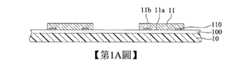
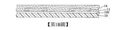
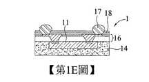
第1A至1E圖係為習知採用晶圓級封裝技術之半導體封裝件1之製法之剖面示意圖。Figures 1A to 1E are schematic cross-sectional views of the conventional manufacturing method of the
如第1A圖所示,形成一熱化離形膠層(thermal release tape)100於一承載件10上。As shown in FIG. 1A, a
接著,置放複數半導體元件11於該熱化離形膠層100上,該些半導體元件11具有相對之作用面11a與非作用面11b,各該作用面11a上具有複數電極墊110,且各該作用面11a黏著於該熱化離形膠層100上。Next, a plurality of
如第1B圖所示,形成一封裝膠體14於該熱化離形膠層100上,以包覆該半導體元件11。As shown in FIG. 1B, an
如第1C圖所示,烘烤該封裝膠體14以硬化該熱化離形膠層100,進而移除該熱化離形膠層100與該承載件10,以外露出該半導體元件11之作用面11a。As shown in FIG. 1C, the
如第1D圖所示,形成一線路結構16於該封裝膠體14與該半導體元件11之作用面11a上,令該線路結構16電性連接該電極墊110。接著,形成一絕緣保護層18於該線路結構16上,且該絕緣保護層18外露該線路結構16之部分表面,以供結合如銲球之導電元件17。As shown in FIG. 1D, a
如第1E圖所示,沿如第1D圖所示之切割路徑L進行切單製程,以獲取複數個半導體封裝件1。As shown in FIG. 1E, the singulation process is performed along the cutting path L shown in FIG. 1D to obtain a plurality of
惟,習知半導體封裝件1,僅於該線路結構16單側設置有半導體元件11,使該半導體封裝件1之功能及效能受限,限制終端電子產品之功能及效能。However, the
因此,如何克服習知技術之種種缺點,實為目前各界亟欲解決之技術問題。Therefore, how to overcome the various shortcomings of the conventional technology is actually a technical problem that all walks of life urgently want to solve.
鑒於上述習知技術之缺失,本發明提供一種電子封裝件之製法,係包括:提供一具有絕緣層之承載板;形成複數導電柱於該絕緣層上,且設置第一電子元件於該絕緣層上;形成包覆層於該絕緣層上,以令該包覆層包覆該第一電子元件與該導電柱,其中,該包覆層係具有相對之第一表面與第二表面,以令該導電柱之端面外露於該包覆層之第一表面,且令該包覆層以其第二表面結合至該絕緣層上;形成線路結構於該包覆層之第一表面上,且令該線路結構電性連接至該導電柱與該第一電子元件;設置第二電子元件於該線路結構上,且令該第二電子元件電性連接該線路結構;以及移除該承載板,且保留該絕緣層。In view of the lack of the above-mentioned conventional technology, the present invention provides a method for manufacturing an electronic package, which includes: providing a carrier board with an insulating layer; forming a plurality of conductive pillars on the insulating layer, and arranging the first electronic element on the insulating layer On; forming a coating layer on the insulating layer so that the coating layer covers the first electronic component and the conductive pillar, wherein the coating layer has a first surface and a second surface opposite to each other, so that The end surface of the conductive pillar is exposed on the first surface of the coating layer, and makesThe coating layer is bonded to the insulating layer with its second surface; forming a circuit structure on the first surface of the coating layer, and electrically connecting the circuit structure to the conductive pillar and the first electronic element; The second electronic element is on the circuit structure, and the second electronic element is electrically connected to the circuit structure; and the carrier board is removed, and the insulating layer is retained.
本發明復提供一種電子封裝件,係包括:包覆層,係具有相對之第一表面與第二表面;第一電子元件,係嵌埋於該包覆層中;複數導電柱,係嵌埋於該包覆層中;線路結構,係設於該包覆層之第一表面上且電性連接該導電柱與該第一電子元件;第二電子元件,係設於該線路結構上且電性連接該線路結構;以及絕緣層,係形成於該包覆層之第二表面上。The present invention further provides an electronic package, which includes: a coating layer having a first surface and a second surface opposite to each other; a first electronic component embedded in the coating layer; a plurality of conductive pillars are embedded In the cladding layer; the circuit structure is arranged on the first surface of the cladding layer and electrically connects the conductive pillar and the first electronic element; the second electronic element is arranged on the circuit structure and electrically The circuit structure is sexually connected; and the insulating layer is formed on the second surface of the cladding layer.
前述之電子封裝件及其製法中,該第一電子元件上係結合及電性連接複數導電體,使該導電體嵌埋於該包覆層中並電性連接該線路結構。例如,該第一電子元件係具有相對之作用面與非作用面,且該作用面結合並電性連接該些導電體;或者,該包覆層之第一表面係齊平該導電體之端面。In the aforementioned electronic package and the manufacturing method thereof, a plurality of conductors are combined and electrically connected to the first electronic component, so that the conductor is embedded in the coating layer and electrically connected to the circuit structure. For example, the first electronic component has opposite active and non-active surfaces, and the active surface is combined and electrically connected to the conductors; or, the first surface of the coating layer is flush with the end surface of the conductor .
前述之電子封裝件及其製法中,該包覆層之第一表面係齊平該導電柱之端面。In the aforementioned electronic package and its manufacturing method, the first surface of the coating layer is flush with the end surface of the conductive pillar.
前述之電子封裝件及其製法中,該第二電子元件係藉由導電凸塊設於該線路結構上以電性連接該線路結構。In the aforementioned electronic package and its manufacturing method, the second electronic element is provided on the circuit structure by conductive bumps to electrically connect the circuit structure.
前述之電子封裝件及其製法中,復包括形成封裝層於該線路結構上,以包覆該第二電子元件。The aforementioned electronic package and its manufacturing method further include forming an encapsulation layer on the circuit structure to cover the second electronic component.
前述之電子封裝件及其製法中,復包括形成線路部於絕緣層上,且令該線路部電性連接該導電柱,例如,該線路部係為電性接觸墊及/或凸塊底下金屬層。進一步包括形成複數導電元件於該線路部上。又包括設置封裝基板於該線路部上。The aforementioned electronic package and its manufacturing method include forming a circuit portion on the insulating layer, and electrically connecting the circuit portion to the conductive post, for example, the circuit portion is an electrical contact pad and/Or the metal layer under the bump. It further includes forming a plurality of conductive elements on the circuit part. It also includes arranging the packaging substrate on the circuit part.
前述之電子封裝件及其製法中,復包括移除該導電柱之端部之部分材質,以令該導電柱於靠近其中一端面之周面形成有凹狀。The aforementioned electronic package and its manufacturing method further include removing part of the material of the end of the conductive pillar, so that the conductive pillar is formed with a concave shape on the peripheral surface close to one end surface of the conductive pillar.
由上可知,本發明之電子封裝件及其製法,主要藉由該線路結構之設計,以接置該第二電子元件,故相較於習知技術,本發明之電子封裝件係在線路結構二側配置有相對位於上、下位置之第一電子元件與第二電子元件,使該電子封裝件具有多功能、高效能之優點。It can be seen from the above that the electronic package of the present invention and its manufacturing method mainly rely on the design of the circuit structure to connect the second electronic component. Therefore, compared with the prior art, the electronic package of the present invention is based on the circuit structure. The first electronic component and the second electronic component located at the upper and lower positions are arranged on the two sides, so that the electronic package has the advantages of multi-function and high performance.
再者,藉由該導電柱之端面作為外接點,可利於控制各該外接點之間的距離,以符合細間距的需求,且能避免各該外接點上之導電元件之間發生橋接。Furthermore, by using the end surface of the conductive column as an external point, the distance between the external points can be controlled to meet the requirement of fine pitch, and the bridging between the conductive elements on the external points can be avoided.
1‧‧‧半導體封裝件1‧‧‧Semiconductor package
10‧‧‧承載件10‧‧‧Carrier
100‧‧‧熱化離形膠層100‧‧‧Thermal release adhesive layer
11‧‧‧半導體元件11‧‧‧Semiconductor components
11a,21a‧‧‧作用面11a,21a‧‧‧action surface
11b,21b‧‧‧非作用面11b,21b‧‧‧Non-acting surface
110,210‧‧‧電極墊110,210‧‧‧electrode pad
14‧‧‧封裝膠體14‧‧‧Packaging gel
16,20‧‧‧線路結構16,20‧‧‧Line structure
17,24,29‧‧‧導電元件17,24,29‧‧‧Conductive element
18‧‧‧絕緣保護層18‧‧‧Insulation protection layer
2‧‧‧電子封裝件2‧‧‧Electronic package
2a‧‧‧封裝基板2a‧‧‧Packaging substrate
2b‧‧‧強固件2b‧‧‧Strong firmware
200‧‧‧絕緣層200‧‧‧Insulation layer
201‧‧‧線路重佈層201‧‧‧Line re-layout
202‧‧‧電性接觸墊202‧‧‧Electrical contact pad
21‧‧‧第一電子元件21‧‧‧The first electronic component
211‧‧‧保護膜211‧‧‧Protective film
212‧‧‧結合層212‧‧‧Combination layer
22‧‧‧導電體22‧‧‧Conductor
22a‧‧‧端面22a‧‧‧end face
23‧‧‧導電柱23‧‧‧Conductive post
23a,23b‧‧‧端面23a,23b‧‧‧end face
23c‧‧‧周面23c‧‧‧Circumference
240,240’‧‧‧線路部240,240’‧‧‧Line Department
25‧‧‧包覆層25‧‧‧Coating
25a‧‧‧第一表面25a‧‧‧First surface
25b‧‧‧第二表面25b‧‧‧Second surface
26‧‧‧第二電子元件26‧‧‧Second electronic component
260‧‧‧底膠260‧‧‧ Primer
27‧‧‧導電凸塊27‧‧‧Conductive bump
270‧‧‧凸塊底下金屬層270‧‧‧Metal layer under bump
28‧‧‧封裝層28‧‧‧Encapsulation layer
9‧‧‧承載板9‧‧‧Carrier plate
9a‧‧‧晶種層9a‧‧‧Seed layer
9b‧‧‧金屬層9b‧‧‧Metal layer
90‧‧‧離型層90‧‧‧Release layer
91‧‧‧絕緣層91‧‧‧Insulation layer
L,S‧‧‧切割路徑L,S‧‧‧cutting path
第1A至1E圖係為習知半導體封裝件之製法的剖面示意圖;以及第2A至2H圖係為本發明之電子封裝件及其製法的剖面示意圖,其中,第2B’圖係為第2B圖之局部放大示意圖,第2G’圖係為第2G圖之另一態樣示意圖。Figures 1A to 1E are cross-sectional schematic diagrams of the manufacturing method of a conventional semiconductor package; and Figures 2A to 2H are cross-sectional schematic diagrams of the electronic package and the manufacturing method of the present invention, wherein Figure 2B' is Figure 2B Fig. 2G' is a schematic diagram of another aspect of Fig. 2G.
以下藉由特定的具體實施例說明本發明之實施方式,熟悉此技藝之人士可由本說明書所揭示之內容輕易地瞭解本發明之其他優點及功效。The following specific examples illustrate the implementation of the present invention. Those familiar with the art can easily understand the other advantages and functions of the present invention from the contents disclosed in this specification.effect.
須知,本說明書所附圖式所繪示之結構、比例、大小等,均僅用以配合說明書所揭示之內容,以供熟悉此技藝之人士之瞭解與閱讀,並非用以限定本發明可實施之限定條件,故不具技術上之實質意義,任何結構之修飾、比例關係之改變或大小之調整,在不影響本發明所能產生之功效及所能達成之目的下,均應仍落在本發明所揭示之技術內容得能涵蓋之範圍內。同時,本說明書中所引用之如「上」、「第一」、「第二」及「一」等之用語,亦僅為便於敘述之明瞭,而非用以限定本發明可實施之範圍,其相對關係之改變或調整,在無實質變更技術內容下,當亦視為本發明可實施之範疇。It should be noted that the structure, ratio, size, etc. shown in the drawings in this manual are only used to match the content disclosed in the manual for the understanding and reading of those who are familiar with the art, and are not intended to limit the implementation of the present invention. Therefore, it does not have any technical significance. Any structural modification, proportional relationship change or size adjustment, without affecting the effects and objectives that can be achieved by the present invention, should still fall within the scope of the present invention. The technical content disclosed by the invention can be covered. At the same time, the terms "on", "first", "second" and "one" cited in this specification are only for ease of description and are not used to limit the scope of the present invention. The change or adjustment of the relative relationship shall be regarded as the scope of the implementation of the present invention without substantial changes to the technical content.
第2A至2H圖係為本發明之電子封裝件2之製法的剖面示意圖。2A to 2H are schematic cross-sectional views of the manufacturing method of the electronic package 2 of the present invention.
如第2A及2B圖所示,提供一具有晶種層9a之承載板9,再於該承載板9上藉由該晶種層9a形成複數導電柱23。接著,設置至少一第一電子元件21於該承載板9上,其中,該第一電子元件21上係結合並電性連接複數導電體22,且該導電體22係為如導電線路、銲球之圓球狀、或如銅柱、銲錫凸塊等金屬材之柱狀、或銲線機製作之釘狀(stud)導電件,但不限於此。As shown in FIGS. 2A and 2B, a
於本實施例中,該承載板9例如為半導體材質(如矽或玻璃)之板體,其上以例如塗佈方式依序形成有一離型層90、如鈦/銅之金屬層9b與一如介電材或防銲材之絕緣層91,以供該晶種層9a設於該絕緣層91上。In this embodiment, the
再者,於第2A圖中,該晶種層9a上可形成有一圖案化阻層(圖略),以令該阻層外露該晶種層9a之部分表面,俾供佈設該些導電柱23。待製作該些導電柱23後,移除該圖案化阻層及其下之晶種層9a,如第2B圖所示,且於蝕刻移除該晶種層9a時,會側蝕該導電柱23之端部,如第2B’圖所示之周面23c,以令該導電柱23之周面23c形成凹狀。Furthermore, in Figure 2A, a patterned resist may be formed on the
又,形成該導電柱23之材質係為如銅之金屬材或銲錫材,且形成該晶種層9a之材質係例如鈦/銅。In addition, the material for forming the
另外,該第一電子元件21係為主動元件、被動元件或其二者組合,且該主動元件係例如半導體晶片,而該被動元件係例如電阻、電容及電感。於本實施例中,該第一電子元件21係為半導體晶片,其具有相對之作用面21a與非作用面21b,該第一電子元件21係以其非作用面21b藉由一結合層212黏固於該絕緣層91上,而該作用面21a具有複數電極墊210與一如鈍化材之保護膜211,且該導電體22形成於該保護膜211中。In addition, the first
如第2C圖所示,形成一包覆層25於該承載板9之絕緣層91上,以令該包覆層25包覆該第一電子元件21、該些導電體22與該些導電柱23,其中,該包覆層25係具有相對之第一表面25a與第二表面25b,且令該保護膜211、該導電體22之端面22a與該導電柱23之端面23a外露於該包覆層25之第一表面25a,以及令該包覆層25以其第二表面25b結合至該承載板9之絕緣層91上。As shown in FIG. 2C, a
於本實施例中,該包覆層25係為絕緣材,如聚醯亞胺(polyimide,簡稱PI)、乾膜(dry film)、如環氧樹脂(epoxy)之封裝膠體或封裝材(molding compound)。例如,該包覆層25之製程可選擇液態封膠(liquid compound)、噴塗(injection)、壓合(lamination)或模壓(compression molding)等方式形成於該絕緣層91上。In this embodiment, the
再者,可藉由整平製程,使該包覆層25之第一表面25a齊平該保護膜211、該導電柱23之端面23a與該導電體22之端面22a,以令該導電柱23之端面23a與該導電體22之端面22a外露於該包覆層25之第一表面25a。例如,該整平製程係藉由研磨方式,移除該保護膜211之部分材質、該導電柱23之部分材質、該導電體22之部分材質與該包覆層25之部分材質。Furthermore, the
又,該些導電柱23之另一端面23b(忽略該晶種層9a)亦可大致齊平該包覆層25之第二表面25b。In addition, the other end surfaces 23b of the conductive pillars 23 (ignoring the
如第2D圖所示,形成一線路結構20於該包覆層25之第一表面25a上,且令該線路結構20電性連接該導電柱23與該導電體22。As shown in FIG. 2D, a
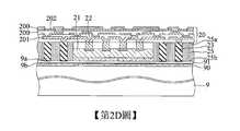
於本實施例中,該線路結構20係包括複數絕緣層200及設於該絕緣層200上之複數線路重佈層(redistribution layer,簡稱RDL)201,且最外層之絕緣層200可作為防銲層,且令最外層之線路重佈層201外露於該防銲層,俾供作為電性接觸墊202,如微墊(micro pad,俗稱μ-pad)。或者,該線路結構20亦可僅包括單一絕緣層200及單一線路重佈層201。In this embodiment, the
再者,形成該線路重佈層201之材質係為銅,且形成該絕緣層200之材質係為如聚對二唑苯(Polybenzoxazole,簡稱PBO)、聚醯亞胺(Polyimide,簡稱PI)、預浸材(Prepreg,簡稱PP)等之介電材、或如綠漆、油墨等之防銲材。Furthermore, the material for forming the
如第2E圖所示,設置至少一第二電子元件26於該線路結構20上,再以一封裝層28包覆該第二電子元件26。As shown in FIG. 2E, at least one second
於本實施例中,該第二電子元件26係為主動元件、被動元件或其二者組合,且該主動元件係例如半導體晶片,而該被動元件係例如電阻、電容及電感。於一實施態樣中,該第二電子元件26係例如為圖形處理器(graphics processing unit,簡稱GPU)、高頻寬記憶體(High Bandwidth Memory,簡稱HBM)等半導體晶片,並無特別限制。In this embodiment, the second
再者,該第二電子元件26係藉由複數如銲錫凸塊、銅凸塊或其它等之導電凸塊27電性連接該電性接觸墊202,且該封裝層28可同時包覆該第二電子元件26與該些導電凸塊27。於本實施例中,可形成一凸塊底下金屬層(Under Bump Metallurgy,簡稱UBM)270於該電性接觸墊202上,以利於結合該導電凸塊27。Furthermore, the second
又,該封裝層28係為絕緣材,如聚醯亞胺(polyimide,簡稱PI)、乾膜(dry film)、如環氧樹脂(expoxy)之封裝膠體或封裝材(molding compound),其可用壓合(lamination)或模壓(molding)之方式形成於該第一線路結構20上。應可理解地,形成該封裝層28之材質可相同或不相同該包覆層25之材質。In addition, the
另外,亦可先形成底膠260於該第二電子元件26與該線路結構20之間以包覆該些導電凸塊27,再形成該封裝層28以包覆該底膠260與該第二電子元件26。In addition, a
如第2F圖所示,移除該承載板9及其上之離型層90與金屬層9b,並保留該絕緣層91。As shown in FIG. 2F, the
於本實施例中,於剝離該離型層90時,藉由該金屬層9b作為阻障之用,以避免破壞該絕緣層91,且待移除該承載板9及其上之離型層90後,再以蝕刻方式移除該金屬層9b。In this embodiment, when the
如第2G圖所示,形成一線路部240於該絕緣層91上以電性連接該導電柱23。As shown in FIG. 2G, a
於本實施例中,該絕緣層91係藉由雷射方式形成有複數開孔,以令該些導電柱23之端面23b及該包覆層25之部分第二表面25b外露於該些開孔,俾供結合該線路部240。例如,該線路部240係為凸塊底下金屬層(UBM),以結合如複數銲錫凸塊或銲球(其規格為C4型)之導電元件24;或者,如第2G’圖所示,該線路部240’係為複數電性接觸墊,其可藉由RDL製程形成於該絕緣層91上,以結合該導電元件24或UBM。In this embodiment, the insulating
再者,可藉由整平製程,如研磨方式,移除該封裝層28之部分材質,使該封裝層28之上表面齊平該第二電子元件26之表面,以令該第二電子元件26外露於該封裝層28。Furthermore, part of the material of the
又,藉由提供具有絕緣層91之承載板9,以於移除該承載板9後,可利用該絕緣層91形成該線路部240,240’,因而無需再佈設介電層,故能節省製程時間與製程步驟,以達到降低製程成本之目的。In addition, by providing the
如第2H圖所示,沿如第2G圖所示之切割路徑S進行切單製程,以獲取複數封裝單元,再將該封裝單元藉由該些導電元件24設置於一封裝基板2a上。As shown in FIG. 2H, a singulation process is performed along the cutting path S shown in FIG. 2G to obtain a plurality of package units, and then the package units are disposed on a
於本實施例中,該封裝基板2a下側進行植球製程以形成複數如銲球之導電元件29,以形成電子封裝件2。於後續製程中,該電子封裝件2可以其封裝基板2a下側之導電元件29設於一電路板(圖略)上。In this embodiment, the underside of the
再者,該封裝基板2a上可依需求設置一強固件2b,如金屬框,以消除應力集中之問題而避免該封裝基板2a發生翹曲之情況。Furthermore, a
因此,本發明之製法中,藉由該線路結構20之電性接觸墊202與該導電柱23之端面23b作為外接點,可利於控制各該外接點之間的距離,以符合細間距的需求,且能避免各該導電凸塊27或各該導電元件24之間發生橋接。Therefore, in the manufacturing method of the present invention, by using the
再者,本發明之製法藉由該線路結構20之設計,以接置該第二電子元件26,故相較於習知技術,本發明之電子封裝件2係在線路結構20二側配置有相對位於上、下位置之第一電子元件20與第二電子元件26,使該電子封裝件2具有多功能、高效能之優點。Furthermore, the manufacturing method of the present invention uses the design of the
本發明亦提供一種電子封裝件2,其包括:一包覆層25、一第一電子元件21、複數導電柱23、一線路結構20、一第二電子元件26以及一線路部240,240’。The present invention also provides an electronic package 2, which includes: a
所述之包覆層25係具有相對之第一表面25a與第二表面25b。The
所述之第一電子元件21係嵌埋於該包覆層25中,且該第一電子元件21上係結合並電性連接複數導電體22,其中,該導電體22係嵌埋於該包覆層25中,且令該導電體22之端面22a外露於該包覆層25之第一表面25a。The first
所述之導電柱23係嵌埋於該包覆層25中,且令該導電柱23之端面22a外露於該包覆層25之第一表面25a。The
所述之線路結構20係設於該包覆層25之第一表面25a上且電性連接該導電柱23與該導電體22。The
所述之第二電子元件26係設於該線路結構20上且電性連接該線路結構20。The second
所述之線路部240,240’係形成於該包覆層25之第二表面25b上且電性連接該導電柱23。The
於一實施例中,該第一電子元件21係具有保護膜211,且該導電體22凸出該保護膜211。In one embodiment, the first
於一實施例中,該第一電子元件21係具有相對之作用面21a與非作用面21b,且該作用面21a結合並電性連接該些導電體22。In one embodiment, the first
於一實施例中,該包覆層25之第一表面25a係齊平該導電柱23之端面23a。In one embodiment, the
於一實施例中,該包覆層25之第二表面25b係齊平該導電柱23之另一端面23b。In one embodiment, the
於一實施例中,該包覆層25之第一表面25a係齊平該導電體22之端面22a。In one embodiment, the
於一實施例中,該第二電子元件26係藉由複數導電凸塊27設於該線路結構20上以電性連接該線路結構20。In one embodiment, the second
於一實施例中,該線路部24係為電性接觸墊及/或凸塊底下金屬層。In one embodiment, the
於一實施例中,所述之電子封裝件2復包括一形成於該線路結構20上之封裝層28,其包覆該第二電子元件26。In one embodiment, the electronic package 2 further includes an
於一實施例中,所述之電子封裝件2復包括一設於該線路部24上之封裝基板2a。In one embodiment, the electronic package 2 further includes a
於一實施例中,該導電柱23於靠近其中一端面23b(或晶種層9a)之周面23c形成有凹狀。In one embodiment, the
綜上所述,本發明之電子封裝件及其製法,係藉由該線路結構與線路部之設計,不僅使封裝件的尺寸較小,且能增加外接點之數量,並且當應用於細間距產品時,可避免各該外接點之間發生橋接。In summary, the electronic package and its manufacturing method of the present invention, through the circuit structure and the design of the circuit part, not only make the size of the package smaller, but also increase the number of external points, and when applied to fine pitch In the case of products, bridging between the external points can be avoided.
上述實施例係用以例示性說明本發明之原理及其功效,而非用於限制本發明。任何熟習此項技藝之人士均可在不違背本發明之精神及範疇下,對上述實施例進行修改。因此本發明之權利保護範圍,應如後述之申請專利範圍所列。The above-mentioned embodiments are used to exemplify the principles and effects of the present invention, but not to limit the present invention. Anyone who is familiar with this technique can modify the above-mentioned embodiments without departing from the spirit and scope of the present invention. Therefore, the scope of protection of the rights of the present invention should be listed in the scope of patent application described later.
2‧‧‧電子封裝件2‧‧‧Electronic package
2a‧‧‧封裝基板2a‧‧‧Packaging substrate
2b‧‧‧強固件2b‧‧‧Strong firmware
20‧‧‧線路結構20‧‧‧Line structure
21‧‧‧第一電子元件21‧‧‧The first electronic component
22‧‧‧導電體22‧‧‧Conductor
23‧‧‧導電柱23‧‧‧Conductive post
24,29‧‧‧導電元件24,29‧‧‧Conductive element
240‧‧‧線路部240‧‧‧Line Department
25‧‧‧包覆層25‧‧‧Coating
25a‧‧‧第一表面25a‧‧‧First surface
25b‧‧‧第二表面25b‧‧‧Second surface
26‧‧‧第二電子元件26‧‧‧Second electronic component
27‧‧‧導電凸塊27‧‧‧Conductive bump
28‧‧‧封裝層28‧‧‧Encapsulation layer
91‧‧‧絕緣層91‧‧‧Insulation layer
Claims (19)
Translated fromChinesePriority Applications (6)
| Application Number | Priority Date | Filing Date | Title |
|---|---|---|---|
| TW108121501ATWI725452B (en) | 2019-06-20 | 2019-06-20 | Electronic package and method for fabricating the same |
| CN201910542299.6ACN112117248B (en) | 2019-06-20 | 2019-06-21 | Electronic package and manufacturing method thereof |
| US16/513,124US11056470B2 (en) | 2019-06-20 | 2019-07-16 | Electronic package and method for fabricating the same |
| US17/337,752US11676948B2 (en) | 2019-06-20 | 2021-06-03 | Method for fabricating electronic package |
| US18/309,756US12176327B2 (en) | 2019-06-20 | 2023-04-28 | Method for fabricating electronic package |
| US18/923,016US20250046771A1 (en) | 2019-06-20 | 2024-10-22 | Method for fabricating electronic package |
Applications Claiming Priority (1)
| Application Number | Priority Date | Filing Date | Title |
|---|---|---|---|
| TW108121501ATWI725452B (en) | 2019-06-20 | 2019-06-20 | Electronic package and method for fabricating the same |
Publications (2)
| Publication Number | Publication Date |
|---|---|
| TW202101713A TW202101713A (en) | 2021-01-01 |
| TWI725452Btrue TWI725452B (en) | 2021-04-21 |
Family
ID=73796700
Family Applications (1)
| Application Number | Title | Priority Date | Filing Date |
|---|---|---|---|
| TW108121501ATWI725452B (en) | 2019-06-20 | 2019-06-20 | Electronic package and method for fabricating the same |
Country Status (3)
| Country | Link |
|---|---|
| US (4) | US11056470B2 (en) |
| CN (1) | CN112117248B (en) |
| TW (1) | TWI725452B (en) |
Families Citing this family (18)
| Publication number | Priority date | Publication date | Assignee | Title |
|---|---|---|---|---|
| TWI725452B (en)* | 2019-06-20 | 2021-04-21 | 矽品精密工業股份有限公司 | Electronic package and method for fabricating the same |
| US11121111B2 (en)* | 2019-09-09 | 2021-09-14 | Advanced Semiconductor Engineering, Inc. | Semiconductor package structure and method of manufacturing the same |
| KR20210152721A (en)* | 2020-06-09 | 2021-12-16 | 삼성전자주식회사 | Semiconductor package |
| KR20220109753A (en) | 2021-01-29 | 2022-08-05 | 삼성전자주식회사 | Semiconductor package including a post |
| US12261163B2 (en) | 2021-04-08 | 2025-03-25 | Taiwan Semiconductor Manufacturing Co., Ltd. | Molded dies in semiconductor packages and methods of forming same |
| US12218041B2 (en) | 2021-04-22 | 2025-02-04 | Qualcomm Incorporated | Integrated circuit (IC) packages employing a capacitor-embedded, redistribution layer (RDL) substrate for interfacing an IC chip(s) to a package substrate, and related methods |
| TWI754586B (en)* | 2021-05-04 | 2022-02-01 | 矽品精密工業股份有限公司 | Electronic package and manufacturing method thereof |
| TWI787805B (en)* | 2021-05-04 | 2022-12-21 | 矽品精密工業股份有限公司 | Electronic module and manufacturing method therefore and electronic package |
| TWI760227B (en)* | 2021-05-19 | 2022-04-01 | 矽品精密工業股份有限公司 | Electronic package and manufacturing method thereof |
| CN113555327A (en)* | 2021-06-21 | 2021-10-26 | 青岛歌尔智能传感器有限公司 | Packaging structure and electronic equipment |
| US11978729B2 (en)* | 2021-07-08 | 2024-05-07 | Taiwan Semiconductor Manufacturing Company, Ltd. | Semiconductor device package having warpage control and method of forming the same |
| US20230060520A1 (en)* | 2021-08-27 | 2023-03-02 | Taiwan Semiconductor Manufacturing Company, Ltd. | Semiconductor package and semiconductor device |
| TWI790916B (en)* | 2022-02-09 | 2023-01-21 | 矽品精密工業股份有限公司 | Electronic package and manufacturing method thereof |
| WO2023159419A1 (en)* | 2022-02-24 | 2023-08-31 | 京东方科技集团股份有限公司 | Array substrate and display device |
| TWI825790B (en)* | 2022-06-17 | 2023-12-11 | 矽品精密工業股份有限公司 | Electronic package and manufacturing method thereof |
| TWI837742B (en)* | 2022-07-26 | 2024-04-01 | 矽品精密工業股份有限公司 | Electronic package and manufacturing method thereof |
| TWI842404B (en)* | 2023-02-20 | 2024-05-11 | 大陸商芯愛科技(南京)有限公司 | Method of electronic package and carrier structure thereof |
| JP2024135584A (en)* | 2023-03-23 | 2024-10-04 | 株式会社東芝 | Storage |
Citations (4)
| Publication number | Priority date | Publication date | Assignee | Title |
|---|---|---|---|---|
| TWI569390B (en)* | 2015-11-16 | 2017-02-01 | 矽品精密工業股份有限公司 | Electronic package and method of manufacture |
| TWI643307B (en)* | 2018-01-30 | 2018-12-01 | 矽品精密工業股份有限公司 | Electronic package and method for fabricating the same |
| TW201919194A (en)* | 2017-11-14 | 2019-05-16 | 台灣積體電路製造股份有限公司 | Package structure |
| CN109817600A (en)* | 2017-11-22 | 2019-05-28 | 矽品精密工业股份有限公司 | Electronic package and method of making the same |
Family Cites Families (13)
| Publication number | Priority date | Publication date | Assignee | Title |
|---|---|---|---|---|
| US6826827B1 (en)* | 1994-12-29 | 2004-12-07 | Tessera, Inc. | Forming conductive posts by selective removal of conductive material |
| JP4961848B2 (en)* | 2006-06-12 | 2012-06-27 | 日本電気株式会社 | WIRING BOARD HAVING METAL POST, SEMICONDUCTOR DEVICE, AND SEMICONDUCTOR DEVICE MODULE MANUFACTURING METHOD |
| US8330272B2 (en)* | 2010-07-08 | 2012-12-11 | Tessera, Inc. | Microelectronic packages with dual or multiple-etched flip-chip connectors |
| CN104051383B (en)* | 2013-03-15 | 2018-02-27 | 台湾积体电路制造股份有限公司 | The semiconductor devices of encapsulation, the method and PoP device for encapsulating semiconductor devices |
| US9627288B2 (en)* | 2015-05-29 | 2017-04-18 | Taiwan Semiconductor Manufacturing Co., Ltd. | Package structures and methods of forming the same |
| TWI822659B (en)* | 2016-10-27 | 2023-11-21 | 美商艾德亞半導體科技有限責任公司 | Structures and methods for low temperature bonding |
| US10763239B2 (en)* | 2017-10-27 | 2020-09-01 | Taiwan Semiconductor Manufacturing Co., Ltd. | Multi-chip wafer level packages and methods of forming the same |
| US11239185B2 (en)* | 2017-11-03 | 2022-02-01 | Dialog Semiconductor (Uk) Limited | Embedded resistor-capacitor film for fan out wafer level packaging |
| US10734323B2 (en)* | 2017-11-22 | 2020-08-04 | Taiwan Semiconductor Manufacturing Co., Ltd. | Package structures |
| US11088124B2 (en)* | 2018-08-14 | 2021-08-10 | Taiwan Semiconductor Manufacturing Company, Ltd. | Package and manufacturing method thereof |
| US11309294B2 (en)* | 2018-09-05 | 2022-04-19 | Taiwan Semiconductor Manufacturing Company, Ltd. | Integrated fan-out packages and methods of forming the same |
| US10665545B2 (en)* | 2018-09-19 | 2020-05-26 | Taiwan Semiconductor Manufacturing Co., Ltd. | Semiconductor devices, semiconductor packages and methods of forming the same |
| TWI725452B (en)* | 2019-06-20 | 2021-04-21 | 矽品精密工業股份有限公司 | Electronic package and method for fabricating the same |
- 2019
- 2019-06-20TWTW108121501Apatent/TWI725452B/ennot_activeIP Right Cessation
- 2019-06-21CNCN201910542299.6Apatent/CN112117248B/enactiveActive
- 2019-07-16USUS16/513,124patent/US11056470B2/enactiveActive
- 2021
- 2021-06-03USUS17/337,752patent/US11676948B2/enactiveActive
- 2023
- 2023-04-28USUS18/309,756patent/US12176327B2/enactiveActive
- 2024
- 2024-10-22USUS18/923,016patent/US20250046771A1/enactivePending
Patent Citations (4)
| Publication number | Priority date | Publication date | Assignee | Title |
|---|---|---|---|---|
| TWI569390B (en)* | 2015-11-16 | 2017-02-01 | 矽品精密工業股份有限公司 | Electronic package and method of manufacture |
| TW201919194A (en)* | 2017-11-14 | 2019-05-16 | 台灣積體電路製造股份有限公司 | Package structure |
| CN109817600A (en)* | 2017-11-22 | 2019-05-28 | 矽品精密工业股份有限公司 | Electronic package and method of making the same |
| TWI643307B (en)* | 2018-01-30 | 2018-12-01 | 矽品精密工業股份有限公司 | Electronic package and method for fabricating the same |
Also Published As
| Publication number | Publication date |
|---|---|
| US20200402965A1 (en) | 2020-12-24 |
| CN112117248A (en) | 2020-12-22 |
| US20210296295A1 (en) | 2021-09-23 |
| TW202101713A (en) | 2021-01-01 |
| US20250046771A1 (en) | 2025-02-06 |
| US12176327B2 (en) | 2024-12-24 |
| US20230268328A1 (en) | 2023-08-24 |
| US11056470B2 (en) | 2021-07-06 |
| CN112117248B (en) | 2022-07-05 |
| US11676948B2 (en) | 2023-06-13 |
Similar Documents
| Publication | Publication Date | Title |
|---|---|---|
| TWI725452B (en) | Electronic package and method for fabricating the same | |
| TWI643307B (en) | Electronic package and method for fabricating the same | |
| TWI676259B (en) | Electronic package and method for fabricating the same | |
| TWI569390B (en) | Electronic package and method of manufacture | |
| TWI714269B (en) | Electronic package and method for manufacturing the same | |
| TWI700796B (en) | Electronic package and manufacturing method thereof | |
| TWI647798B (en) | Electronic package and its manufacturing method | |
| TWI712149B (en) | Electronic package and method for fabricating the same | |
| TWI760227B (en) | Electronic package and manufacturing method thereof | |
| CN116130425A (en) | Electronic package and method for manufacturing the same | |
| TWI767770B (en) | Electronic package and manufacturing method thereof | |
| CN109037179B (en) | Electronic package and method of making the same | |
| TWI790916B (en) | Electronic package and manufacturing method thereof | |
| TWI718801B (en) | Electronic package manufacturing method | |
| CN117316884A (en) | Electronic package and method for manufacturing the same | |
| TWI883713B (en) | Electronic package and manufacturing method thereof | |
| TWI854498B (en) | Electronic package and fabricating method thereof | |
| TWI809787B (en) | Electronic package and manufacturing method thereof | |
| CN119890171A (en) | Electronic packaging and method of manufacturing the same | |
| CN119920809A (en) | Electronic packaging and method of manufacturing the same |
Legal Events
| Date | Code | Title | Description |
|---|---|---|---|
| MM4A | Annulment or lapse of patent due to non-payment of fees |