TWI725364B - Transparent substrate with holes and manufacturing method thereof - Google Patents
Transparent substrate with holes and manufacturing method thereofDownload PDFInfo
- Publication number
- TWI725364B TWI725364BTW107144817ATW107144817ATWI725364BTW I725364 BTWI725364 BTW I725364BTW 107144817 ATW107144817 ATW 107144817ATW 107144817 ATW107144817 ATW 107144817ATW I725364 BTWI725364 BTW I725364B
- Authority
- TW
- Taiwan
- Prior art keywords
- transparent substrate
- hole
- laser beam
- diameter
- protection layer
- Prior art date
Links
Images


Landscapes
- Laser Beam Processing (AREA)
- Re-Forming, After-Treatment, Cutting And Transporting Of Glass Products (AREA)
Abstract
Translated fromChineseDescription
Translated fromChinese本發明係關於一種透明基板結構及加工方法,特別關於在透明基板結構加工製作穿孔之結構和方法,尤其改善穿孔製程造成的前後段孔洞過度外闊問題。The present invention relates to a transparent substrate structure and processing method, in particular to a structure and method for processing and making perforations in the transparent substrate structure, and particularly to improve the problem of excessively widening of the front and rear holes caused by the perforation process.
近年來在智能手機、5G通信和物聯網等應用開發的先進封裝技術必須滿足以下要求:a)高性能;b)微型化;c)成本低;d)多功能;承上,而導致有以下原因,在一個芯片中實現所有系統功能存在基本挑戰:a)分離的功能塊之間的干擾;b)不同技術節點的設計複雜性和過程限制;c)成本考慮;因此,已經提出了垂直互連的3D IC堆疊,以實現比傳統2D封裝技術更高的性能,更低的功耗和更小的佔用面積。In recent years, advanced packaging technologies developed in applications such as smart phones, 5G communications and the Internet of Things must meet the following requirements: a) high performance; b) miniaturization; c) low cost; d) multi-function; The reason is that there are basic challenges in implementing all system functions in one chip: a) interference between separated functional blocks; b) design complexity and process limitations of different technology nodes; c) cost considerations; therefore, a vertical interaction has been proposed. Connected 3D IC stack to achieve higher performance than traditional 2D packaging technology, lower power consumption and smaller footprint.
目前的中介層材料主要基於矽或塑料;其中,採用矽通孔(Through-Silicon Vias,TSV)製造的矽中介層可以實現所需的佈線和I/O密度,但不具成本效益;另,塑料中介層提供了成本有效的解決方案,但由於其較差的尺寸穩定性和與硅晶片不匹配的熱膨脹係數(Coefficient of thermal expansion,CTE)而面臨若干挑戰;因此,由於其有利的材料特性,已經使用玻璃作為替代中介層;玻璃的熱膨脹係數低且與硅類似,這提供了良好的熱穩定性;此外,玻璃具有高電阻率,與硅相比,導致更低的插入損耗和串擾;且,玻璃的優異機械強度提供了超薄和柔韌基板的可能性,並且玻璃具有成本效益;因此,所有這些特性都表明玻璃將是一種出色的電子中介材料。The current interposer materials are mainly based on silicon or plastic; among them, the silicon interposer made of Through-Silicon Vias (TSV) can achieve the required wiring and I/O density, but it is not cost-effective; in addition, plastic The interposer provides a cost-effective solution, but faces several challenges due to its poor dimensional stability and coefficient of thermal expansion (CTE) that does not match the silicon wafer; therefore, due to its favorable material properties, it has Use glass as an alternative interposer; glass has a low thermal expansion coefficient and is similar to silicon, which provides good thermal stability; in addition, glass has a high resistivity, which leads to lower insertion loss and crosstalk compared to silicon; and, The excellent mechanical strength of glass provides the possibility of ultra-thin and flexible substrates,And glass is cost-effective; therefore, all these characteristics indicate that glass will be an excellent electronic intermediary material.
儘管玻璃具有如上所述的許多優點,但仍然存在許多需要解決的挑戰;玻璃的基本材料限制是它是脆性材料,並且它具有非常低的導熱性。Although glass has many advantages as described above, there are still many challenges to be solved; the basic material limitation of glass is that it is a brittle material and it has very low thermal conductivity.
其中,在實作常見的穿孔加工,因穿孔加工常導致裂紋形成,然而裂紋形成對結構性和可靠性有深遠的影響;玻璃穿孔可以通過多種方式實施,最常見者為玻璃中的孔洞經受高功率雷射燒蝕的照射以形成通孔。因此,需深入研究了不同類型的雷射和光束各類製程以減少裂紋形成。Among them, in the implementation of common perforation processing, the perforation processing often leads to the formation of cracks, but the formation of cracks has a profound impact on the structure and reliability; glass perforation can be implemented in many ways, the most common one is that the holes in the glass withstand high Power laser ablation irradiation to form through holes. Therefore, it is necessary to in-depth study of different types of lasers and beam processes to reduce the formation of cracks.
TGV雷射鑽孔技術對短距離和高通孔密度的需求提供了可行性,並通過玻璃基板的低導熱性改善了熱管理;為此,它進一步增加了無裂紋通孔製作的挑戰。另外,玻璃和銅金屬化之間的熱膨脹係數不匹配導致界面處的高熱機械應力;這種應力可能在可靠性試驗期間引起疲勞相關的失效問題,特別是在表面裂紋存在的情況下。TGV laser drilling technology provides feasibility for the short distance and high through hole density requirements, and improves thermal management through the low thermal conductivity of the glass substrate; for this reason, it further increases the challenge of crack-free through hole production. In addition, the thermal expansion coefficient mismatch between glass and copper metallization results in high thermomechanical stress at the interface; this stress may cause fatigue-related failure problems during reliability testing, especially in the presence of surface cracks.
此外,在金屬化期間可以在通孔中形成空隙,其受到通孔的表面粗糙度和通孔的幾何形狀的影響。通過金屬層的沉積,金屬原子在一定的錐角內朝向目標表面移動,因此更難以在深溝槽處獲得金屬化的完全覆蓋;這種空洞或所謂的“釘頭”在通孔中形成金屬化會引起電流擁擠和額外的“熱點”,依據研究,這些熱機械應力會導致通孔的退化;因此,需要一種錐形通孔,在通孔處具有一定的傾斜側壁。In addition, voids can be formed in the through holes during metallization, which are affected by the surface roughness of the through holes and the geometry of the through holes. Through the deposition of the metal layer, the metal atoms move towards the target surface within a certain cone angle, so it is more difficult to obtain complete coverage of the metallization at the deep trench; this kind of cavity or so-called "nail head" forms the metallization in the through hole It will cause current congestion and additional "hot spots". According to research, these thermo-mechanical stresses will cause the degradation of the through hole; therefore, a tapered through hole is required with a certain inclined sidewall at the through hole.
雷射已被廣泛用於進行材料的燒蝕和表面處理;通常,多脈衝雷射束聚焦到物體表面或物體內部的一個點,接著消融的狀況取決於吸收機制和雷射參數,例如波長和脈衝持續時間。當激發時間短於材料中的熱化時間時,可發生非熱與光化學燒蝕,其中直接電離和緻密電子空穴等離子體的形成可導致直接斷裂,並且晶格爆炸性崩解通過Bremsstrahlung(電子排斥)。材料去除伴隨著從輻射區域噴射的高度定向的羽流。緻密蒸汽羽流可包含固體和液體的材料簇。Lasers have been widely used for ablation and surface treatment of materials; usually, multi-pulseThe impulsive laser beam is focused to a point on the surface or inside of the object, and then the ablation status depends on the absorption mechanism and laser parameters, such as wavelength and pulse duration. When the excitation time is shorter than the thermalization time in the material, non-thermal and photochemical ablation can occur, in which direct ionization and the formation of dense electron-hole plasma can lead to direct rupture, and the explosive disintegration of the crystal lattice through Bremsstrahlung (electron Exclusion). Material removal is accompanied by a highly directed plume ejected from the radiation area. The dense vapor plume can contain clusters of solid and liquid materials.
通常,較短的脈衝雷射,能量更快地施加到材料中,導致更快速的材料噴射;由雷射直接激發的材料體積在噴射之前將能量轉移到周圍材料的時間較短;因此,燒蝕體積由雷射的空間輪廓和光學穿透深度更精確地限定,並且剩餘材料具有更少的殘餘能量,這減少了玻璃中裂縫的形成。然而,當使用多脈衝雷射光束來燒蝕材料時,材料的表面紋理,形態和化學的累積變化可能發生,甚至可以在具有高於閾值的過剩能量的單個雷射脈衝發生。這通常被認為是由雷射照射引起的材料改變。在玻璃的情況下,這些材料改質可用於進一步的玻璃加工,例如化學蝕刻,以在玻璃中產生某些圖案或通孔。Generally, with a shorter pulse laser, energy is applied to the material faster, resulting in faster material ejection; the volume of material directly excited by the laser transfers energy to the surrounding material for a shorter time before ejection; therefore, burning The erosion volume is more precisely defined by the laser's spatial profile and optical penetration depth, and the remaining material has less residual energy, which reduces the formation of cracks in the glass. However, when a multi-pulse laser beam is used to ablate a material, cumulative changes in the surface texture, morphology, and chemistry of the material may occur, even in a single laser pulse with excess energy above the threshold. This is generally considered to be a material change caused by laser irradiation. In the case of glass, these material modifications can be used for further glass processing, such as chemical etching, to create certain patterns or through holes in the glass.
然而,用於玻璃應用的無裂紋和精確限定範圍的材料改質區,在理想情況下需要使用超高速雷射,如皮秒或飛秒脈衝雷射,只需一次射擊即可在整個基板上形成通道,並且熱影響體積最小,能量剛好超過閾值能量是燒蝕玻璃的有利雷射條件。其中聚焦的高斯光束,由於橫向擴展,高強度可以維持的距離相對較短,再根據Rayleigh準則,焦深(DOF)是波長的問題,與數值孔徑(NA)和束腰直徑相反的問題;因此,焦深(DOF)隨著腰部直徑(或增加的峰值強度)和數值孔徑(NA)值而減小,具有高NA透鏡的高斯光束形成將輻射聚焦成微米尺寸的光斑。另,貝塞爾光束引入了一種更有效的方法,只需一個脈衝即可生成這種長孔洞,有利於將準貝塞爾光束雷射用於諸如玻璃的透明材料的燒蝕應用。However, the crack-free and precisely defined range of material modification areas for glass applications require ultra-high-speed lasers, such as picosecond or femtosecond pulse lasers, in ideal situations, which can be applied to the entire substrate with only one shot The formation of channels, and the smallest heat-affected volume, and the energy just exceeding the threshold energy are favorable laser conditions for ablating glass. Among them, the focused Gaussian beam, due to the lateral expansion, the distance that high intensity can maintain is relatively short, and according to the Rayleigh criterion, the depth of focus (DOF) is a problem of wavelength, which is the opposite of numerical aperture (NA) and beam waist diameter; therefore , The depth of focus (DOF) decreases with the waist diameter (or increased peak intensity) and numerical aperture (NA) value, with highThe Gaussian beam of the NA lens forms a spot that focuses the radiation into a micrometer size. In addition, the Bessel beam introduces a more effective method of generating such long holes with only one pulse, which is conducive to the use of quasi-Bessel beam lasers for ablation applications of transparent materials such as glass.
準貝塞爾雷射光束的主要特徵是焦點是一個焦點線,而不是一個點;理想的貝塞爾光束需要焦距無限遠的透鏡直徑,並且包含無限能量,因此是不現實的;而,近似貝塞爾光束或準貝塞爾光束可以通過截斷理想平面波來實現,從而產生有限的焦距;在實踐中,已經使用不同的方法來生成準貝塞爾光束;這些包括通過將高斯光束與軸錐透鏡聚焦以產生貝塞爾高斯光束,在凸透鏡的焦平面中放置環形孔徑並使用空間光調製器(Spatial Light Mmodulator,SLM)或衍射光束整形元件(Diffractive Optical Beam Shaping Element,DOE)用於在雷射光束上施加相位分佈。The main feature of a quasi-Bessel laser beam is that the focal point is a focal line, not a point; an ideal Bessel beam requires a lens diameter with an infinite focal length and contains infinite energy, so it is unrealistic; and, approximate A Bessel beam or a quasi-Bessel beam can be realized by truncating an ideal plane wave, resulting in a finite focal length; in practice, different methods have been used to generate a quasi-Bessel beam; these include by combining a Gaussian beam with an axicon The lens is focused to generate a Bessel Gaussian beam, the annular aperture is placed in the focal plane of the convex lens and a spatial light modulator (SLM) or a diffractive optical beam shaping element (DOE) is used in the laser beam. Impose a phase distribution on the incident beam.
以下例舉數篇先前技術文獻,多個相關專利如下:US 13/958,346揭示一種藉由雷射絲化作用在材料加工穿孔之裝置、系統及方法,該雷射絲化作用係使用一種將入射雷射光束以一分散方式沿縱向光束軸聚焦的光學組態。這分散式聚焦方法可在多段距離上形成絲,且該雷射及聚焦參數係調整成可決定該絲的增長及結束點,以產生一單/雙端封閉孔,或一貫穿孔。由一堆疊或套疊組態選擇之透明基板可具有在不影響相鄰基板之情形下形成在其中或穿過其中之多數孔。這些分散式聚焦方法將支持在硼矽玻璃及類似的易碎材料及半導體中形成具有遠超過十毫米的多種長度之絲。The following are several examples of prior art documents, and a number of related patents are as follows: US 13/958,346 discloses a device, system and method for processing and perforating materials by laser filamentation. An optical configuration in which the laser beam is focused along the longitudinal beam axis in a dispersed manner. This decentralized focusing method can form filaments over multiple distances, and the laser and focusing parameters are adjusted to determine the growth and end points of the filaments to produce a single/double-ended closed hole or a through hole. The transparent substrate selected by a stacked or nested configuration may have a plurality of holes formed in or through the adjacent substrates without affecting the adjacent substrates. These decentralized focusing methods will support the formation of filaments with a variety of lengths far exceeding ten millimeters in borosilicate glass and similar fragile materials and semiconductors.
US 61/871,440揭示藉由雷射鑽孔及酸蝕刻在玻璃基板中形成通孔之方法。在一個實施例中,一種在玻璃基板中形成通孔之方法包括以下步驟:自該玻璃基板之入射表面雷射鑽鑿該通孔穿過該玻璃基板之厚度的至少一部分。該方法進一步包括以下步驟:蝕刻該玻璃基板歷時蝕刻持續時間以增大該通孔之入射開口之直徑,且在該蝕刻持續時間的至少一部分期間將超音波能量施加至該玻璃基板。所施加的超音波能量具有在40kHz與192kHz之間的頻率。US 61/871,440 discloses a method for forming through holes in a glass substrate by laser drilling and acid etching. In one embodiment, a method of forming a through hole in a glass substrate includesThe following steps: laser drilling the through hole through at least a part of the thickness of the glass substrate from the incident surface of the glass substrate. The method further includes the steps of etching the glass substrate for an etching duration to increase the diameter of the entrance opening of the through hole, and applying ultrasonic energy to the glass substrate during at least a portion of the etching duration. The ultrasonic energy applied has a frequency between 40kHz and 192kHz.
US 61/418,152揭示一種在玻璃中製造高密度的孔洞陣列的方法,該方法包含以下步驟:提供具有前表面的玻璃塊(glass piece),隨後以UV雷射束照射該玻璃塊的該前表面,該UV雷射束被聚焦到焦點,該焦點在該玻璃塊的該前表面的+/- 100μm內,最期望是在該前表面的+/- 50μm內。聚焦該雷射的該透鏡具有數值孔徑,對於0.3mm至0.63mm之間的玻璃厚度而言,期望上該數值孔徑是在從0.1至0.4的範圍內,更期望是在0.1至0.15的範圍內,更加期望是在0.12至0.13的範圍內,以便產生開啟的孔洞,該等開啟的孔洞從該玻璃塊的該前表面102延伸進入該玻璃塊100,該等孔洞具有範圍從5μm至15μm的直徑及至少20:1的深寬比。對於較薄的玻璃而言(範圍在0.1-0.3mm),該數值孔徑期望上是從0.25至0.4,更期望是從0.25至0.3,而該雷射束較佳為聚焦至該玻璃的該前表面的+/-30μm之內。期望上是以約15kHz以下的重覆速率操作雷射。因此產生的孔洞陣列可隨後透過蝕刻而擴大。如果需要,則該前表面可在蝕刻之前受到研磨。US 61/418,152 discloses a method for manufacturing a high-density hole array in glass, the method includes the following steps: providing a glass piece with a front surface, and then irradiating the front surface of the glass piece with a UV laser beam The UV laser beam is focused to a focal pointthat is within +/- 100 μm of the front surface of the glass block, most desirably within +/- 50μm of the front surface. The lens that focuses the laser has a numerical aperture. For a glass thickness between 0.3 mm and 0.63 mm, it is desirable that the numerical aperture is in the range from 0.1 to 0.4, more desirably in the range from 0.1 to 0.15 It is more desirable to be in the range of 0.12 to 0.13 in order to generate open holes, the open holes extending from the front surface 102 of the glass block into the glass block 100, the holes having a range from 5μm to 15A diameter of μ m and an aspect ratio of at least 20:1. For thinner glass (range 0.1-0.3mm), the numerical aperture is desirably from 0.25 to 0.4, more desirably from 0.25 to 0.3, and the laser beam is preferably focused to the front of the glass Within +/-30μm of the surface. It is desirable to operate the laser at a repetition rate below about 15kHz. The resulting array of holes can then be enlarged by etching. If necessary, the front surface can be ground before etching.
然而,當預期連續孔洞加工如第6a圖所示,極易因雷射孔洞射出段呈現擴孔問題呈現如第6b圖狀況,為解決此問題,本發明之主要目的係在提供一種具有孔洞之透明基板及其製造方法,以改善上述問題。However, when the continuous hole processing is expected as shown in Figure 6a, it is very easy for the laser hole ejection section to show the problem of reaming as shown in Figure 6b. In order to solve this problem, the main purpose of the present invention is to provide a hole with holes. The transparent substrate and the manufacturing method thereof can improve the above-mentioned problems.
有鑑於以上問題,本發明係提供一種具有孔洞之透明基板及其製造方法,由一光學保護層將雷射導引到透明基板之外區域。In view of the above problems, the present invention provides a transparent substrate with holes and a manufacturing method thereof. An optical protective layer guides the laser to the area outside the transparent substrate.
因此,本發明之主要目的係在提供一種具有孔洞之透明基板及其製造方法,經由光學保護層將多餘雷射引導到透明基板之外區域,減少加工孔洞出現擴孔現象。Therefore, the main purpose of the present invention is to provide a transparent substrate with holes and a manufacturing method thereof, which guide excess lasers to areas outside the transparent substrate through the optical protective layer, and reduce the phenomenon of hole expansion in processing holes.
本發明再一目的係在提供一種具有孔洞之透明基板及其製造方法,藉由改善雷射加工之擴孔現象,使後段加工良率提升。Another object of the present invention is to provide a transparent substrate with holes and a manufacturing method thereof, which improves the post-processing yield by improving the hole expansion phenomenon of laser processing.
本發明再一目的係在提供一種具有孔洞之透明基板及其製造方法,利用減少雷射折射到透明基板,可達成更小孔徑的挖孔。Another object of the present invention is to provide a transparent substrate with holes and a manufacturing method thereof. By reducing the laser refraction to the transparent substrate, a hole with a smaller aperture can be achieved.
本發明再一目的係在提供一種具有孔洞之透明基板及其製造方法,憑藉簡單於透明基板下方設置光學保護層,可不需增加工時情況下完成品質提升。Another object of the present invention is to provide a transparent substrate with holes and a manufacturing method thereof. By simply disposing an optical protective layer under the transparent substrate, the quality can be improved without increasing man-hours.
為達到上述目的,本發明所使用的主要技術手段是採用以下技術方案來實現的。本發明為一種具有孔洞之透明基板,其包含:一透明基板包含一貫穿孔及一改質區,該透明基板的材料為玻璃、藍寶石、氧化鋅之透明材料;其特徵在於:當該透明基板置於一光學保護層之一透光面之上,以一脈衝雷射光束聚焦於該透明基板製作該貫穿孔,此時沿著該貫穿孔外圍產生該改質區,而加工殘留之該脈衝雷射光束透射至該光學保護層之該透光面,由該光學保護層將加工殘留之該脈衝雷射光束導引至該光學保護層之一導光面,最後該貫穿孔貫通於該透明基板。In order to achieve the above objective, the main technical means used in the present invention are achieved by the following technical solutions. The present invention is a transparent substrate with holes, which includes: a transparent substrate including a through hole and a modified area; the material of the transparent substrate is a transparent material of glass, sapphire, and zinc oxide; it is characterized in that: when the transparent substrate is placed On a light-transmitting surface of an optical protection layer, a pulsed laser beam is focused on the transparent substrate to make the through hole. At this time, the modified area is generated along the periphery of the through hole, and the remaining pulsed mine is processed The light beam is transmitted to the light-transmitting surface of the optical protection layer, and the processed pulse laser beam is guided by the optical protection layer to a light-guiding surface of the optical protection layer, and finally the through hole penetrates the transparent substrate .
本發明的目的及解決其技術問題還可採用以下技術措施步驟進一步實現。The purpose of the present invention and the solution of its technical problems can be further achieved by adopting the following technical measures.
前述的透明基板,其中該光學保護層可以是水、雷射保護液、膠帶、光阻液、膠之液體或固體材料。In the aforementioned transparent substrate, the optical protective layer can be water, laser protective liquid, adhesive tape, photoresist liquid, glue liquid or solid material.
前述的透明基板,該貫穿孔的直徑小於或等於80μm。In the aforementioned transparent substrate, the diameter of the through hole is less than or equal to 80 μm.
前述的透明基板,該貫穿孔的直徑小於或等於60μm。In the aforementioned transparent substrate, the diameter of the through hole is less than or equal to 60 μm.
前述的透明基板,該貫穿孔的直徑小於或等於40μm。In the aforementioned transparent substrate, the diameter of the through hole is less than or equal to 40 μm.
前述的透明基板,該貫穿孔的直徑小於或等於30μm。In the aforementioned transparent substrate, the diameter of the through hole is less than or equal to 30 μm.
前述的透明基板,該貫穿孔的中段直徑大於表面直徑的50%。In the aforementioned transparent substrate, the diameter of the middle section of the through hole is greater than 50% of the surface diameter.
另,為達成上述目地,本發明所使用的再一主要技術手段是採用以下技術方案來實現的。本發明為一種具有孔洞之透明基板製造方法,包含:步驟1:將一透明基板置於一光學保護層之一透光面之上;步驟2:以一脈衝雷射光束聚焦於該透明基板製作一貫穿孔,此時沿著該貫穿孔外圍產生一改質區;步驟3:當加工殘留之該脈衝雷射光束透射至該光學保護層之該透光面,由該光學保護層將加工殘留之該脈衝雷射光束導引至該光學保護層之一導光面;步驟4:以該脈衝雷射光束聚焦形成該貫穿孔貫通於該透明基板。In addition, in order to achieve the above objective, another main technical means used in the present invention is achieved by adopting the following technical solutions. The present invention is a method for manufacturing a transparent substrate with holes, including: Step 1: Place a transparent substrate on a light-transmitting surface of an optical protection layer; Step 2: Use a pulsed laser beam to focus on the transparent substrate. A through hole, at this time, a modified area is generated along the periphery of the through hole; Step 3: When the processed residual pulsed laser beam is transmitted to the transparent surface of the optical protection layer, the remaining processed area will be processed by the optical protection layer The pulsed laser beam is guided to a light guide surface of the optical protection layer; Step 4: Focusing the pulsed laser beam to form the through hole penetrating the transparent substrate.
本發明的目的及解決其技術問題還可採用以下技術措施步驟進一步實現。The purpose of the present invention and the solution of its technical problems can be further achieved by adopting the following technical measures.
前述的方法,在步驟4之後,將該透明基板浸泡在一酸液中,以使該貫穿孔擴大。In the foregoing method, after step 4, the transparent substrate is immersed in an acid solution to enlarge the through hole.
前述的方法,其中該光學保護層可以是水、雷射保護液、膠帶、光阻液、膠之液體或固體材料。In the aforementioned method, the optical protection layer may be water, laser protection liquid, tape, photoresist liquid, glue liquid or solid material.
前述的方法,其中該酸液具有氟化氫成分。The aforementioned method, wherein the acid solution has a hydrogen fluoride component.
前述的方法製得之透明基板,其中:該透明基板的材料為玻璃、藍寶石、氧化鋅之透明材料;於該脈衝雷射光束貫通該透明基板,該貫穿孔形成於該透明基板中;該貫穿孔的直徑小於30μm,該貫穿孔的中段直徑大於表面直徑的50%。The transparent substrate prepared by the foregoing method, wherein: the transparent substrate is made of glass, sapphire, and zinc oxide transparent material; when the pulsed laser beam penetrates the transparent substrate, the through hole is formed in the transparent substrate; The diameter of the hole is less than 30 μm, and the diameter of the middle section of the through hole is greater than 50% of the surface diameter.
相較於習知技術,本發明具有功效在於:(1)利用光學保護層將多餘雷射引導到透明基板之外區域,減少加工孔洞出現擴孔現象缺點;(2)藉由改善雷射加工之擴孔現象,使後段加工良率提升;(3)減少雷射折射到透明基板,可達成更小孔徑的挖孔;(4)憑藉簡單於透明基板下方設置光學保護層,可不需增加工時情況下完成品質提升。Compared with the conventional technology, the present invention has the following effects: (1) The optical protective layer is used to guide the excess laser to the area outside the transparent substrate, reducing the disadvantages of hole reaming in the processing hole; (2) By improving the laser processing The hole reaming phenomenon improves the yield rate of the subsequent processing; (3) reduces the laser refraction to the transparent substrate, which can achieve a smaller hole digging; (4) by simply setting the optical protection layer under the transparent substrate, there is no need to increase labor Complete quality improvement under all circumstances.
10:透明基板10: Transparent substrate
11:貫穿孔11: Through hole
12:改質區12: Modified area
20:光學保護層20: Optical protection layer
21:透光面21: Translucent surface
22:導光面22: light guide surface
30:脈衝雷射光束30: Pulse laser beam
31:對焦點31: Focus
32:散射雷射光束32: Scattering laser beam
33:折射雷射光束33: Refraction laser beam
40:酸液40: Acid
51:步驟151: Step 1
52:步驟252: Step 2
53:步驟353: Step 3
54:步驟454: Step 4
55:步驟555:
第1a圖:為本發明之第一流程圖;第1b圖:為本發明之第二流程圖;第2圖:為本發明之最佳實施型態之第一示意圖;第3a圖:為本發明之最佳實施型態之第二示意圖;第3b圖:為本發明之最佳實施型態之第三示意圖;第4a圖:為本發明之最佳實施型態之第一剖面圖;第4b圖:為本發明之最佳實施型態之第二剖面圖;第4c圖:為本發明之最佳實施型態之第三剖面圖;第4d圖:為本發明之最佳實施型態之第四剖面圖;第4e圖:為本發明之最佳實施型態之第五剖面圖;第5a圖:為本發明之最佳實施型態之第一雷射示意圖;第5b圖:為本發明之最佳實施型態之第二雷射示意圖;第5c圖:為本發明之最佳實施型態之第三雷射示意圖;第6a圖:為本發明之先前技術之預期示意圖;第6b圖:為本發明之先前技術之實際示意圖;第7圖:為本發明之最佳實施型態之第四示意圖。Figure 1a: is the first flow chart of the present invention; Figure 1b: is the second flow chart of the present invention; Figure 2: is the first schematic diagram of the best embodiment of the present invention; Figure 3a: is this The second schematic diagram of the best embodiment of the invention; Figure 3b: the third schematic diagram of the best embodiment of the invention; Figure 4a: the first cross-sectional view of the best embodiment of the invention; Figure 4b: is the second cross-sectional view of the best embodiment of the present invention; Figure 4c: is the third cross-sectional view of the best embodiment of the present invention; Figure 4d: is the best embodiment of the present invention The fourth cross-sectional view; Fig. 4e: the fifth cross-sectional view of the best embodiment of the present invention; Fig. 5a: The first laser schematic view of the best embodiment of the present invention;Figure 5b: a schematic diagram of the second laser of the best embodiment of the present invention; Figure 5c: a schematic diagram of the third laser of the best embodiment of the present invention; Figure 6a: the prior art of the present invention Figure 6b: the actual schematic diagram of the prior art of the present invention; Figure 7: the fourth schematic diagram of the best embodiment of the present invention.
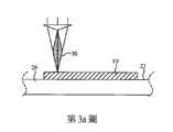
為了讓本發明之目的、特徵與功效更明顯易懂,以下特別列舉本發明之較佳實施型態:請先參考第3a圖所示,本發明一種具有孔洞之透明基板包含一透明基板(10)、一光學保護層(20)及一脈衝雷射光束(30)。In order to make the purpose, features and effects of the present invention more comprehensible, the following specifically enumerates the preferred embodiments of the present invention: please refer to Figure 3a first, a transparent substrate with holes of the present invention includes a transparent substrate (10 ), an optical protection layer (20) and a pulsed laser beam (30).
具體而言,該透明基板(10)的材料為玻璃、藍寶石、氧化鋅等透明材料;而,該光學保護層(20)可以是水、雷射保護液、膠帶、光阻液、膠等液體或固體材料;該脈衝雷射光束(30)係為『雷射加工』實行之聚焦後之雷射,其中『雷射加工』是利用雷射光的高強度、高平行度的特徵以聚焦鏡等光學裝置將之聚為功率密度達103~109瓦/平方公分的光點後,在工件的表面產生局部的加熱熔化、氣化等熱效應而達到加工的目的。由於從光能轉換成熱能的時間非常短,加上功率密度相當高,在單位時間、單位面積內提供極高的光能,使得材料的表面在瞬間內便可獲得大量的熱能。此種使材料表面升溫的速度一般可達每秒數千度,在雷射加工的過程極容易發生『液體/氣體』或『固體/氣體』的混合模式。Specifically, the material of the transparent substrate (10) is transparent materials such as glass, sapphire, zinc oxide, etc.; and the optical protection layer (20) may be liquids such as water, laser protection liquid, adhesive tape, photoresist liquid, glue, etc. Or solid material; the pulsed laser beam (30) is a focused laser performed by "laser processing", where "laser processing" uses the high-intensity and high parallelism characteristics of laser light to focus mirrors, etc. After the optical device condenses it into a light spot with a power density of 103 to 109 watts/cm², local heating, melting, vaporization and other thermal effects are generated on the surface of the workpiece to achieve the purpose of processing. Because the time to convert light energy to heat energy is very short, and the power density is quite high, it provides extremely high light energy per unit time and unit area, so that the surface of the material can obtain a large amount of heat energy in an instant. This kind of rate of heating the surface of the material can generally reach thousands of degrees per second, and the "liquid/gas" or "solid/gas" mixed mode is very prone to occur in the laser processing process.
其中,該透明基板(10)包含一貫穿孔(11)及一改質區(12);其貫穿孔(11)係指設於該透明基板(10)表面最終須貫通之加工孔洞,該貫穿孔(11)先行由雷射方式貫通;該改質區(12)係指是指該貫穿孔(11)於雷射加工過程產生於貫穿孔(11)周遭之區域,其因為該透明基板(10)接受雷射光線照射如以上『雷射加工』解釋,導致該貫穿孔(11)周圍材料被改質,導致該改質區(12)材料密度產生變化,該改質區(12)之外徑約為1~20微米(μm,Micrometer)。Wherein, the transparent substrate (10) includes a through hole (11) and a modified region (12); the through hole (11) refers to a processing hole provided on the surface of the transparent substrate (10) that must be penetrated finally,The through hole (11) is first penetrated by a laser; the modified area (12) refers to the area where the through hole (11) is generated around the through hole (11) during the laser processing process because of the transparency The substrate (10) is irradiated by laser light, as explained in the above "laser processing", which causes the material around the through hole (11) to be modified, resulting in a change in the material density of the modified area (12), and the modified area (12) The outer diameter of) is about 1-20 microns (μm, Micrometer).
再,依本案結構加工,該貫穿孔(11)的直徑可小於或等於80μm;或,該貫穿孔(11)的直徑可小於或等於60μm;或,該貫穿孔(11)的直徑可小於或等於40μm;或,該貫穿孔(11)的直徑可小於或等於30μm。Furthermore, according to the structure of the present case, the diameter of the through hole (11) can be less than or equal to 80 μm; or, the diameter of the through hole (11) can be less than or equal to 60 μm; or, the diameter of the through hole (11) can be less than or It is equal to 40 μm; or, the diameter of the through hole (11) may be less than or equal to 30 μm.
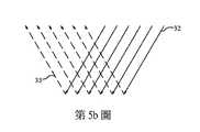
請參閱第5a圖所示,此圖係為脈衝雷射光束(30)聚焦表示,可見脈衝雷射光束(30)聚焦在對焦點(31),同時有複數散射雷射光束(32)從脈衝雷射光束(30)周遭分離;接著,請看第5b圖當複數散射雷射光束(32)遇到大氣內各類介質產生折射雷射光束(33),而折射雷射光束(33)極有可能導致雷射加工目標外的破壞;而見第5c圖所示,可在複數散射雷射光束(32)路徑上設置光學保護層(20)將折射雷射光束(33)引導到雷射加工目標外。Please refer to Figure 5a. This figure shows the focus of the pulsed laser beam (30). It can be seen that the pulsed laser beam (30) is focused on the focus point (31), and there is a complex scattered laser beam (32) from the pulse The laser beam (30) is separated around; then, please see Fig. 5b. When the complex scattering laser beam (32) encounters various media in the atmosphere, it produces a refracted laser beam (33), and the refracted laser beam (33) is extremely It may cause damage outside the laser processing target; as shown in Figure 5c, an optical protective layer (20) can be set on the path of the complex scattered laser beam (32) to guide the refracted laser beam (33) to the laser Outside the processing target.
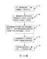
請再參考第1圖所示,該圖為本案之主要方法,其包含:首先,請參考第1圖之步驟1(51)與第2圖表示,步驟1(51)係將一透明基板(10)置於一光學保護層(20)之一透光面(21)之上。Please refer to Figure 1 again. This figure is the main method of this project. It includes: First, please refer to step 1 (51) and Figure 2 of Figure 1. Step 1 (51) is to put a transparent substrate ( 10) It is placed on a transparent surface (21) of an optical protection layer (20).
在此步驟1(51)目的係為將透明基板(10)與光學保護層(20)之透光面(21)貼合,避免空氣殘留。The purpose of this step 1 (51) is to attach the transparent substrate (10) to the light-transmitting surface (21) of the optical protection layer (20) to avoid air residue.
接著,再參考第1圖之步驟2(52)、第3a與3b圖表示,步驟2(52)係以一脈衝雷射光束(30)聚焦於該透明基板(10)製作一貫穿孔(11),此時沿著該貫穿孔(11)外圍產生一改質區(12)。Next, referring to step 2 (52), 3a and 3b of Figure 1, step 2 (52) is to focus a pulsed laser beam (30) on the transparent substrate (10) to make a through hole(11) At this time, a modified area (12) is generated along the periphery of the through hole (11).
在此步驟2(52)目的係為由脈衝雷射光束(30)加工於該透明基板(10)產生貫穿孔(11)與改質區(12);其貫穿孔(11)在該透明基板(10)剖面狀態可參閱第4a圖,可見在透明基板(10)表面產生直徑T0之貫穿孔(11)。In this step 2 (52), the purpose is to process the transparent substrate (10) by the pulsed laser beam (30) to produce the through hole (11) and the modified area (12); the through hole (11) is in the transparent substrate (10) For the cross-sectional state, refer to Figure 4a. It can be seen that a through hole (11) of diameter T0 is formed on the surface of the transparent substrate (10).
再,可參考第1圖之步驟3(53),其狀態在第4b圖時,步驟3(53)係當加工殘留之該脈衝雷射光束(30)透射至該光學保護層(20)之該透光面(21),由該光學保護層(20)將加工殘留之該脈衝雷射光束(30)導引至該光學保護層(20)之一導光面(22)。Furthermore, please refer to step 3 (53) in Figure 1. When the state is in Figure 4b, step 3 (53) is when the remaining pulsed laser beam (30) is transmitted to the optical protection layer (20). The transparent surface (21) is guided by the optical protection layer (20) to the remaining pulsed laser beam (30) to a light guide surface (22) of the optical protection layer (20).
在此步驟3(53)目的係為將加工殘留之脈衝雷射光束(30)導引至該光學保護層(20)之一導光面(22),避免空氣折射導致透明基板(10)承接加工殘留之脈衝雷射光束(30)。The purpose of this step 3 (53) is to guide the remaining pulsed laser beam (30) of the processing to a light guide surface (22) of the optical protective layer (20), to avoid air refraction and cause the transparent substrate (10) to accept Process the remaining pulsed laser beam (30).
又,請再參考第1圖之步驟4(54)、第4c與4d圖表示,步驟4(54)係以該脈衝雷射光束(30)聚焦形成該貫穿孔(11)貫通於該透明基板(10)。Also, please refer to step 4 (54), 4c and 4d of Figure 1 again. In step 4 (54), the pulsed laser beam (30) is focused to form the through hole (11) through the transparent substrate. (10).
在此步驟4(54)目的係為承上步驟3(53)貫通該透明基板(10);其加工過程從步驟3(53)之第4a圖開始,在第4b圖中透明基板(10)表面產生直徑T1之貫穿孔(11),有光學保護層(20)在透明基板(10)下方可見第4d圖位於透明基板(10)背面之貫穿孔(11)呈現直徑D1之狀態;另,如無光學保護層(20)在透明基板(10)下方可見第4c圖位於透明基板(10)背面之貫穿孔(11)呈現直徑D0之擴孔狀態。The purpose of step 4 (54) here is to follow step 3 (53) through the transparent substrate (10); the processing process starts from Figure 4a of step 3 (53), and the transparent substrate (10) in Figure 4b A through hole (11) with a diameter of T1 is formed on the surface, and an optical protective layer (20) can be seen under the transparent substrate (10) in Figure 4d. The through hole (11) on the back of the transparent substrate (10) has a diameter of D1; If there is no optical protective layer (20) under the transparent substrate (10), it can be seen that the through hole (11) on the back of the transparent substrate (10) in Figure 4c shows a reamed state of diameter D0.
依以上方法製得之透明基板具有以下特徵。該透明基板的材料為玻璃、藍寶石、氧化鋅等透明材料;於該脈衝雷射光束貫通該透明基板,該貫穿孔形成於該透明基板中;該貫穿孔的直徑小於30μm,該貫穿孔的中段直徑大於表面直徑的50%(可見第4e圖該貫穿孔的中段直徑C1大於該貫穿孔的表面直徑T3或D2的50%)。The transparent substrate prepared by the above method has the following characteristics. The material of the transparent substrateThe material is a transparent material such as glass, sapphire, zinc oxide; when the pulsed laser beam penetrates the transparent substrate, the through hole is formed in the transparent substrate; the diameter of the through hole is less than 30 μm, and the middle diameter of the through hole is larger than the surface diameter (It can be seen in Figure 4e that the diameter C1 of the middle section of the through hole is greater than 50% of the surface diameter T3 or D2 of the through hole).
一般而言,可參考第1b圖會在在步驟4(54)之後接續步驟5(55),該步驟4(54)係將該透明基板(10)浸泡在一酸液(40)中,以使該貫穿孔(11)擴大。Generally speaking, referring to Figure 1b, step 5 (55) will be continued after step 4 (54). Step 4 (54) involves immersing the transparent substrate (10) in an acid solution (40) to The through hole (11) is enlarged.
在此步驟5(55)目的係為將第3b圖所示之改質區(12)藉由第7圖之酸液(40)將該透明基板(10)之該貫穿孔(11)周遭之改質區(12)腐蝕,貫穿孔(11)狀態由第4d圖轉變為第4e圖;其中,該酸液(40)具有氟化氫成分。The purpose of this step 5 (55) is to use the acid solution (40) shown in Figure 7 in the modified area (12) shown in Figure 3b to surround the through hole (11) of the transparent substrate (10). The modified zone (12) is corroded, and the state of the through hole (11) is changed from Figure 4d to Figure 4e; wherein the acid solution (40) has a hydrogen fluoride component.
為更加明確表示本實施例,以下將依序介紹實際實行概況。In order to express this embodiment more clearly, the following will introduce the actual implementation overview in order.
首先,如第2圖所示,將一透明基板(10)置於一光學保護層(20)之一透光面(21)之上,使透明基板(10)與光學保護層(20)之透光面(21)貼合,無空氣於兩者間。First, as shown in Figure 2, a transparent substrate (10) is placed on a transparent surface (21) of an optical protective layer (20), so that the transparent substrate (10) and the optical protective layer (20) are The light-transmitting surface (21) is attached, and there is no air in between.
接著,參考第3a圖,脈衝雷射光束(30)聚焦於該透明基板(10)製作一貫穿孔(11)如第4a圖,此時沿著該貫穿孔(11)外圍產生一改質區(12)如第3b圖;此時,透明基板(10)表面產生直徑T0之貫穿孔(11)。Next, referring to Figure 3a, the pulsed laser beam (30) is focused on the transparent substrate (10) to make a through hole (11) as shown in Figure 4a. At this time, a modified region (11) is formed along the periphery of the through hole (11). 12) As shown in Figure 3b; at this time, a through hole (11) of diameter T0 is formed on the surface of the transparent substrate (10).
又,在第4b圖時,當該脈衝雷射光束(30)透射至該光學保護層(20)之該透光面(21),如5c圖表達由該光學保護層(20)將該脈衝雷射光束(30)產生之散射雷射光束(32)導引至該光學保護層(20)之一導光面(22),避免空氣折射導致透明基板(10)承接加工殘留之散射雷射光束(32);此時,透明基板(10)表面產生直徑T1之貫穿孔(11)。In addition, in Figure 4b, when the pulsed laser beam (30) is transmitted to the light-transmitting surface (21) of the optical protective layer (20), as shown in Figure 5c, the pulsed laser beam (30) is expressed by the optical protective layer (20). The scattered laser beam (32) generated by the laser beam (30) is guided to the optical protection layer (20)A light guide surface (22) prevents the transparent substrate (10) from receiving the residual scattered laser beam (32) due to air refraction; at this time, a through hole (11) with a diameter of T1 is formed on the surface of the transparent substrate (10).
再,第4d圖中,以該脈衝雷射光束(30)聚焦形成該貫穿孔(11)貫通於該透明基板(10);此時,透明基板(10)表面貫穿孔(11)為直徑T2,透明基板(10)背面貫穿孔(11)為直徑D1,可見第4e圖該貫穿孔的中段直徑C0大於該貫穿孔的表面直徑T2或D1的50%。Furthermore, in Figure 4d, the pulsed laser beam (30) is focused to form the through hole (11) to penetrate through the transparent substrate (10); at this time, the through hole (11) on the surface of the transparent substrate (10) has a diameter of T2 The through hole (11) on the back of the transparent substrate (10) has a diameter D1. It can be seen that the middle diameter C0 of the through hole in Figure 4e is greater than 50% of the surface diameter T2 or D1 of the through hole.
最後,如第7圖將該透明基板(10)浸泡在酸液(40)中,以使該貫穿孔(11)擴大狀態由第4d圖轉變為第4e圖。Finally, as shown in Fig. 7, the transparent substrate (10) is immersed in an acid solution (40), so that the expanded state of the through hole (11) is changed from Fig. 4d to Fig. 4e.
因此本發明之功效有別於一般透明基板製作穿孔方法,此於半導體業內當中實屬首創,符合發明專利要件,爰依法俱文提出申請。Therefore, the effect of the present invention is different from that of a general transparent substrate manufacturing method. It is the first in the semiconductor industry and meets the requirements of an invention patent. The application is filed in accordance with the law.
惟,需再次重申,以上所述者僅為本發明之較佳實施型態,舉凡應用本發明說明書、申請專利範圍或圖式所為之等效變化,仍屬本發明所保護之技術範疇,因此本發明之保護範圍當視後附之申請專利範圍所界定者為準。However, it needs to be reiterated that the above are only the preferred implementation modes of the present invention. Any equivalent changes made by applying the specification, patent application scope, or drawings of the present invention still belong to the technical scope protected by the present invention. Therefore, The scope of protection of the present invention shall be subject to those defined by the attached patent scope.
10:透明基板10: Transparent substrate
20:光學保護層20: Optical protection layer
21:透光面21: Translucent surface
30:脈衝雷射光束30: Pulse laser beam
Claims (11)
Translated fromChinesePriority Applications (1)
| Application Number | Priority Date | Filing Date | Title |
|---|---|---|---|
| TW107144817ATWI725364B (en) | 2018-12-12 | 2018-12-12 | Transparent substrate with holes and manufacturing method thereof |
Applications Claiming Priority (1)
| Application Number | Priority Date | Filing Date | Title |
|---|---|---|---|
| TW107144817ATWI725364B (en) | 2018-12-12 | 2018-12-12 | Transparent substrate with holes and manufacturing method thereof |
Publications (2)
| Publication Number | Publication Date |
|---|---|
| TW202021705A TW202021705A (en) | 2020-06-16 |
| TWI725364Btrue TWI725364B (en) | 2021-04-21 |
Family
ID=72175552
Family Applications (1)
| Application Number | Title | Priority Date | Filing Date |
|---|---|---|---|
| TW107144817ATWI725364B (en) | 2018-12-12 | 2018-12-12 | Transparent substrate with holes and manufacturing method thereof |
Country Status (1)
| Country | Link |
|---|---|
| TW (1) | TWI725364B (en) |
Families Citing this family (1)
| Publication number | Priority date | Publication date | Assignee | Title |
|---|---|---|---|---|
| TWI744135B (en)* | 2020-12-15 | 2021-10-21 | 鈦昇科技股份有限公司 | Multi-focus laser forming method of through hole |
Citations (2)
| Publication number | Priority date | Publication date | Assignee | Title |
|---|---|---|---|---|
| CN1845812A (en)* | 2003-07-31 | 2006-10-11 | 康宁股份有限公司 | A method of making at least one hole in a transparent body and devices made by this method |
| CN106029286A (en)* | 2013-12-17 | 2016-10-12 | 康宁股份有限公司 | Method for rapid laser drilling in glass and products made therefrom |
- 2018
- 2018-12-12TWTW107144817Apatent/TWI725364B/enactive
Patent Citations (2)
| Publication number | Priority date | Publication date | Assignee | Title |
|---|---|---|---|---|
| CN1845812A (en)* | 2003-07-31 | 2006-10-11 | 康宁股份有限公司 | A method of making at least one hole in a transparent body and devices made by this method |
| CN106029286A (en)* | 2013-12-17 | 2016-10-12 | 康宁股份有限公司 | Method for rapid laser drilling in glass and products made therefrom |
Also Published As
| Publication number | Publication date |
|---|---|
| TW202021705A (en) | 2020-06-16 |
Similar Documents
| Publication | Publication Date | Title |
|---|---|---|
| KR101333518B1 (en) | Laser machining method, laser cutting method, and method for dividing structure having multilayer board | |
| TWI584906B (en) | Method and apparatus for non-abaltive, photoaccoustic compression machining in transparent materials using filamentation by burst ultrafast laser pulses | |
| CN105392593B (en) | Apparatus and method for cutting contours from flat substrates by means of laser | |
| CN107835794A (en) | Method for continuous manufacture of holes in flexible substrate sheet and products related thereto | |
| JP2009544145A (en) | Wafer scribing with an infrared laser using short pulses | |
| JP2017502901A (en) | Cutting stack transparent materials using ultrafast laser beam optics, destructive layers and other layers | |
| TW201141646A (en) | Method and apparatus for scribing a line in a thin film using a series of laser pulses | |
| KR20110110238A (en) | Cutting device and method for cutting electronic parts | |
| JP2011104633A (en) | Scribing method | |
| TWI725364B (en) | Transparent substrate with holes and manufacturing method thereof | |
| CN115666003B (en) | Circuit board blind slot manufacturing method and system | |
| TWI237532B (en) | Carbon dioxide laser processing method for laminated material | |
| US20070145024A1 (en) | Laser via drilling apparatus and methods | |
| US20250087500A1 (en) | Method for preparing fcbga package substrate | |
| US20170131556A1 (en) | Laser via drilling apparatus and methods | |
| US20240113072A1 (en) | Singulation of integrated circuit package substrates with glass cores | |
| TWI698401B (en) | Method for manufacturing perforation of glass substrate | |
| TWI715138B (en) | Bessel laser system with variable zoom mechanism | |
| Martens et al. | Laser-based target preparation in 3D integrated electronic packages | |
| Gobet et al. | Implementation of short-pulse lasers for wafer scribing and grooving applications | |
| RU2546719C1 (en) | Method of obtaining relief on surface | |
| Franz et al. | Ultrashort Pulsed Laser Drilling of Printed Circuit Board Materials. Materials 2022, 15, 3932 | |
| CN109202297A (en) | A kind of laser wet etch process suitable for arbitrary surface transparent dielectric material | |
| CN119927443B (en) | A gallium nitride material etching method and etching system | |
| US20240112970A1 (en) | Singulation of integrated circuit package substrates with glass cores |