TWI725356B - Semiconductor device and method for manufacturing the same - Google Patents
Semiconductor device and method for manufacturing the sameDownload PDFInfo
- Publication number
- TWI725356B TWI725356BTW107142130ATW107142130ATWI725356BTW I725356 BTWI725356 BTW I725356BTW 107142130 ATW107142130 ATW 107142130ATW 107142130 ATW107142130 ATW 107142130ATW I725356 BTWI725356 BTW I725356B
- Authority
- TW
- Taiwan
- Prior art keywords
- source
- isolation
- region
- isolation region
- pair
- Prior art date
Links
- 239000004065semiconductorSubstances0.000titleclaimsabstractdescription110
- 238000000034methodMethods0.000titleclaimsdescription21
- 238000004519manufacturing processMethods0.000titleclaimsdescription14
- 238000002955isolationMethods0.000claimsabstractdescription187
- 239000000758substrateSubstances0.000claimsabstractdescription59
- 239000002019doping agentSubstances0.000claimsdescription13
- 239000012535impuritySubstances0.000claimsdescription3
- 239000010410layerSubstances0.000description65
- 229910052751metalInorganic materials0.000description17
- 239000002184metalSubstances0.000description17
- 239000000463materialSubstances0.000description14
- 238000010586diagramMethods0.000description10
- 125000006850spacer groupChemical group0.000description8
- 229910000577Silicon-germaniumInorganic materials0.000description6
- 230000015556catabolic processEffects0.000description6
- 238000001459lithographyMethods0.000description6
- LEVVHYCKPQWKOP-UHFFFAOYSA-N[Si].[Ge]Chemical compound[Si].[Ge]LEVVHYCKPQWKOP-UHFFFAOYSA-N0.000description4
- 239000012212insulatorSubstances0.000description4
- 238000000059patterningMethods0.000description4
- XUIMIQQOPSSXEZ-UHFFFAOYSA-NSiliconChemical compound[Si]XUIMIQQOPSSXEZ-UHFFFAOYSA-N0.000description3
- 150000001875compoundsChemical class0.000description3
- 238000005498polishingMethods0.000description3
- 229910052710siliconInorganic materials0.000description3
- 239000010703siliconSubstances0.000description3
- -1silicon oxideChemical class0.000description3
- 239000000126substanceSubstances0.000description3
- JBRZTFJDHDCESZ-UHFFFAOYSA-NAsGaChemical compound[As]#[Ga]JBRZTFJDHDCESZ-UHFFFAOYSA-N0.000description2
- 229910005540GaPInorganic materials0.000description2
- 229910001218Gallium arsenideInorganic materials0.000description2
- 229910000673Indium arsenideInorganic materials0.000description2
- GPXJNWSHGFTCBW-UHFFFAOYSA-NIndium phosphideChemical compound[In]#PGPXJNWSHGFTCBW-UHFFFAOYSA-N0.000description2
- VYPSYNLAJGMNEJ-UHFFFAOYSA-NSilicium dioxideChemical compoundO=[Si]=OVYPSYNLAJGMNEJ-UHFFFAOYSA-N0.000description2
- 238000000137annealingMethods0.000description2
- 230000015572biosynthetic processEffects0.000description2
- 239000002131composite materialSubstances0.000description2
- 238000005530etchingMethods0.000description2
- HZXMRANICFIONG-UHFFFAOYSA-Ngallium phosphideChemical compound[Ga]#PHZXMRANICFIONG-UHFFFAOYSA-N0.000description2
- 229910052732germaniumInorganic materials0.000description2
- GNPVGFCGXDBREM-UHFFFAOYSA-Ngermanium atomChemical compound[Ge]GNPVGFCGXDBREM-UHFFFAOYSA-N0.000description2
- RPQDHPTXJYYUPQ-UHFFFAOYSA-Nindium arsenideChemical compound[In]#[As]RPQDHPTXJYYUPQ-UHFFFAOYSA-N0.000description2
- 238000009413insulationMethods0.000description2
- 239000011229interlayerSubstances0.000description2
- HBMJWWWQQXIZIP-UHFFFAOYSA-Nsilicon carbideChemical compound[Si+]#[C-]HBMJWWWQQXIZIP-UHFFFAOYSA-N0.000description2
- 229910010271silicon carbideInorganic materials0.000description2
- 229910052814silicon oxideInorganic materials0.000description2
- 238000004088simulationMethods0.000description2
- 229910052581Si3N4Inorganic materials0.000description1
- 230000003247decreasing effectEffects0.000description1
- 239000002305electric materialSubstances0.000description1
- 230000005669field effectEffects0.000description1
- 238000002513implantationMethods0.000description1
- 239000011810insulating materialSubstances0.000description1
- 238000005468ion implantationMethods0.000description1
- 229910044991metal oxideInorganic materials0.000description1
- 150000004706metal oxidesChemical class0.000description1
- 230000004048modificationEffects0.000description1
- 238000012986modificationMethods0.000description1
- 229920002120photoresistant polymerPolymers0.000description1
- HQVNEWCFYHHQES-UHFFFAOYSA-Nsilicon nitrideChemical compoundN12[Si]34N5[Si]62N3[Si]51N64HQVNEWCFYHHQES-UHFFFAOYSA-N0.000description1
- 238000006467substitution reactionMethods0.000description1
Images


Classifications
- H—ELECTRICITY
- H01—ELECTRIC ELEMENTS
- H01L—SEMICONDUCTOR DEVICES NOT COVERED BY CLASS H10
- H01L21/00—Processes or apparatus adapted for the manufacture or treatment of semiconductor or solid state devices or of parts thereof
- H01L21/70—Manufacture or treatment of devices consisting of a plurality of solid state components formed in or on a common substrate or of parts thereof; Manufacture of integrated circuit devices or of parts thereof
- H01L21/71—Manufacture of specific parts of devices defined in group H01L21/70
- H01L21/76—Making of isolation regions between components
- H01L21/761—PN junctions
- H—ELECTRICITY
- H01—ELECTRIC ELEMENTS
- H01L—SEMICONDUCTOR DEVICES NOT COVERED BY CLASS H10
- H01L21/00—Processes or apparatus adapted for the manufacture or treatment of semiconductor or solid state devices or of parts thereof
- H01L21/70—Manufacture or treatment of devices consisting of a plurality of solid state components formed in or on a common substrate or of parts thereof; Manufacture of integrated circuit devices or of parts thereof
- H01L21/71—Manufacture of specific parts of devices defined in group H01L21/70
- H01L21/76—Making of isolation regions between components
- H01L21/762—Dielectric regions, e.g. EPIC dielectric isolation, LOCOS; Trench refilling techniques, SOI technology, use of channel stoppers
- H01L21/7624—Dielectric regions, e.g. EPIC dielectric isolation, LOCOS; Trench refilling techniques, SOI technology, use of channel stoppers using semiconductor on insulator [SOI] technology
- H01L21/76264—SOI together with lateral isolation, e.g. using local oxidation of silicon, or dielectric or polycristalline material refilled trench or air gap isolation regions, e.g. completely isolated semiconductor islands
- H—ELECTRICITY
- H10—SEMICONDUCTOR DEVICES; ELECTRIC SOLID-STATE DEVICES NOT OTHERWISE PROVIDED FOR
- H10D—INORGANIC ELECTRIC SEMICONDUCTOR DEVICES
- H10D84/00—Integrated devices formed in or on semiconductor substrates that comprise only semiconducting layers, e.g. on Si wafers or on GaAs-on-Si wafers
- H10D84/01—Manufacture or treatment
- H10D84/0107—Integrating at least one component covered by H10D12/00 or H10D30/00 with at least one component covered by H10D8/00, H10D10/00 or H10D18/00, e.g. integrating IGFETs with BJTs
- H10D84/0109—Integrating at least one component covered by H10D12/00 or H10D30/00 with at least one component covered by H10D8/00, H10D10/00 or H10D18/00, e.g. integrating IGFETs with BJTs the at least one component covered by H10D12/00 or H10D30/00 being a MOS device
- H—ELECTRICITY
- H10—SEMICONDUCTOR DEVICES; ELECTRIC SOLID-STATE DEVICES NOT OTHERWISE PROVIDED FOR
- H10D—INORGANIC ELECTRIC SEMICONDUCTOR DEVICES
- H10D84/00—Integrated devices formed in or on semiconductor substrates that comprise only semiconducting layers, e.g. on Si wafers or on GaAs-on-Si wafers
- H10D84/01—Manufacture or treatment
- H10D84/0123—Integrating together multiple components covered by H10D12/00 or H10D30/00, e.g. integrating multiple IGBTs
- H10D84/0126—Integrating together multiple components covered by H10D12/00 or H10D30/00, e.g. integrating multiple IGBTs the components including insulated gates, e.g. IGFETs
- H10D84/0158—Integrating together multiple components covered by H10D12/00 or H10D30/00, e.g. integrating multiple IGBTs the components including insulated gates, e.g. IGFETs the components including FinFETs
- H—ELECTRICITY
- H10—SEMICONDUCTOR DEVICES; ELECTRIC SOLID-STATE DEVICES NOT OTHERWISE PROVIDED FOR
- H10D—INORGANIC ELECTRIC SEMICONDUCTOR DEVICES
- H10D84/00—Integrated devices formed in or on semiconductor substrates that comprise only semiconducting layers, e.g. on Si wafers or on GaAs-on-Si wafers
- H10D84/01—Manufacture or treatment
- H10D84/02—Manufacture or treatment characterised by using material-based technologies
- H10D84/03—Manufacture or treatment characterised by using material-based technologies using Group IV technology, e.g. silicon technology or silicon-carbide [SiC] technology
- H10D84/038—Manufacture or treatment characterised by using material-based technologies using Group IV technology, e.g. silicon technology or silicon-carbide [SiC] technology using silicon technology, e.g. SiGe
- H—ELECTRICITY
- H10—SEMICONDUCTOR DEVICES; ELECTRIC SOLID-STATE DEVICES NOT OTHERWISE PROVIDED FOR
- H10D—INORGANIC ELECTRIC SEMICONDUCTOR DEVICES
- H10D84/00—Integrated devices formed in or on semiconductor substrates that comprise only semiconducting layers, e.g. on Si wafers or on GaAs-on-Si wafers
- H10D84/80—Integrated devices formed in or on semiconductor substrates that comprise only semiconducting layers, e.g. on Si wafers or on GaAs-on-Si wafers characterised by the integration of at least one component covered by groups H10D12/00 or H10D30/00, e.g. integration of IGFETs
- H10D84/811—Combinations of field-effect devices and one or more diodes, capacitors or resistors
- H—ELECTRICITY
- H10—SEMICONDUCTOR DEVICES; ELECTRIC SOLID-STATE DEVICES NOT OTHERWISE PROVIDED FOR
- H10D—INORGANIC ELECTRIC SEMICONDUCTOR DEVICES
- H10D84/00—Integrated devices formed in or on semiconductor substrates that comprise only semiconducting layers, e.g. on Si wafers or on GaAs-on-Si wafers
- H10D84/80—Integrated devices formed in or on semiconductor substrates that comprise only semiconducting layers, e.g. on Si wafers or on GaAs-on-Si wafers characterised by the integration of at least one component covered by groups H10D12/00 or H10D30/00, e.g. integration of IGFETs
- H10D84/82—Integrated devices formed in or on semiconductor substrates that comprise only semiconducting layers, e.g. on Si wafers or on GaAs-on-Si wafers characterised by the integration of at least one component covered by groups H10D12/00 or H10D30/00, e.g. integration of IGFETs of only field-effect components
- H10D84/83—Integrated devices formed in or on semiconductor substrates that comprise only semiconducting layers, e.g. on Si wafers or on GaAs-on-Si wafers characterised by the integration of at least one component covered by groups H10D12/00 or H10D30/00, e.g. integration of IGFETs of only field-effect components of only insulated-gate FETs [IGFET]
- H10D84/834—Integrated devices formed in or on semiconductor substrates that comprise only semiconducting layers, e.g. on Si wafers or on GaAs-on-Si wafers characterised by the integration of at least one component covered by groups H10D12/00 or H10D30/00, e.g. integration of IGFETs of only field-effect components of only insulated-gate FETs [IGFET] comprising FinFETs
- H—ELECTRICITY
- H10—SEMICONDUCTOR DEVICES; ELECTRIC SOLID-STATE DEVICES NOT OTHERWISE PROVIDED FOR
- H10D—INORGANIC ELECTRIC SEMICONDUCTOR DEVICES
- H10D86/00—Integrated devices formed in or on insulating or conducting substrates, e.g. formed in silicon-on-insulator [SOI] substrates or on stainless steel or glass substrates
- H10D86/01—Manufacture or treatment
- H10D86/011—Manufacture or treatment comprising FinFETs
- H—ELECTRICITY
- H10—SEMICONDUCTOR DEVICES; ELECTRIC SOLID-STATE DEVICES NOT OTHERWISE PROVIDED FOR
- H10D—INORGANIC ELECTRIC SEMICONDUCTOR DEVICES
- H10D86/00—Integrated devices formed in or on insulating or conducting substrates, e.g. formed in silicon-on-insulator [SOI] substrates or on stainless steel or glass substrates
- H10D86/201—Integrated devices formed in or on insulating or conducting substrates, e.g. formed in silicon-on-insulator [SOI] substrates or on stainless steel or glass substrates the substrates comprising an insulating layer on a semiconductor body, e.g. SOI
- H10D86/215—Integrated devices formed in or on insulating or conducting substrates, e.g. formed in silicon-on-insulator [SOI] substrates or on stainless steel or glass substrates the substrates comprising an insulating layer on a semiconductor body, e.g. SOI comprising FinFETs
- H—ELECTRICITY
- H10—SEMICONDUCTOR DEVICES; ELECTRIC SOLID-STATE DEVICES NOT OTHERWISE PROVIDED FOR
- H10D—INORGANIC ELECTRIC SEMICONDUCTOR DEVICES
- H10D62/00—Semiconductor bodies, or regions thereof, of devices having potential barriers
- H10D62/10—Shapes, relative sizes or dispositions of the regions of the semiconductor bodies; Shapes of the semiconductor bodies
- H10D62/17—Semiconductor regions connected to electrodes not carrying current to be rectified, amplified or switched, e.g. channel regions
- H10D62/351—Substrate regions of field-effect devices
- H10D62/357—Substrate regions of field-effect devices of FETs
- H10D62/364—Substrate regions of field-effect devices of FETs of IGFETs
- H10D62/371—Inactive supplementary semiconductor regions, e.g. for preventing punch-through, improving capacity effect or leakage current
Landscapes
- Engineering & Computer Science (AREA)
- Physics & Mathematics (AREA)
- Condensed Matter Physics & Semiconductors (AREA)
- General Physics & Mathematics (AREA)
- Manufacturing & Machinery (AREA)
- Computer Hardware Design (AREA)
- Microelectronics & Electronic Packaging (AREA)
- Power Engineering (AREA)
- Insulated Gate Type Field-Effect Transistor (AREA)
- Metal-Oxide And Bipolar Metal-Oxide Semiconductor Integrated Circuits (AREA)
Abstract
Description
Translated fromChinese本發明實施例係有關於半導體裝置及其製造方法。The embodiment of the present invention relates to a semiconductor device and a manufacturing method thereof.
諸如淺溝槽隔離(shallow trench isolation;STI)之隔離區被用於在相鄰半導體裝置,諸如金屬氧化物半導體(metal oxide semiconductor;MOS)裝置,之間提供預期之隔離效果。為改良MOS裝置之效能,諸如應用矽鍺(SiGe)源極/汲極區之應力工程設計整合至MOS裝置中。另外,提出由相鄰MOS裝置共用的連續主動區,以進一步增強MOS裝置的效能。需要在連續主動區之相鄰MOS裝置的源極/汲極區之間提供足夠的隔離效果。Isolation regions such as shallow trench isolation (STI) are used to provide the desired isolation between adjacent semiconductor devices, such as metal oxide semiconductor (MOS) devices. In order to improve the performance of MOS devices, for example, the stress engineering design of silicon germanium (SiGe) source/drain regions is integrated into the MOS device. In addition, a continuous active region shared by adjacent MOS devices is proposed to further enhance the performance of MOS devices. It is necessary to provide sufficient isolation between the source/drain regions of adjacent MOS devices in the continuous active region.
本發明的一實施例揭露一種半導體裝置,其包含:一基板;在該基板上的一對電晶體裝置,其中該對該等電晶體裝置中之每一者包含一通道、在該通道上方的一閘極電極,及在該閘極電極旁邊之一源極/汲極區;及在該對該等電晶體裝置之該等源極/汲極區之間的一隔離區,其中該隔離區具有一第一摻雜類型,該第一摻雜類型與該等源極/汲極區之一第二摻雜類型相反。An embodiment of the present invention discloses a semiconductor device comprising: a substrate; a pair of transistor devices on the substrate, wherein each of the pair of transistor devices includes a channel, A gate electrode, and a source/drain region next to the gate electrode; and an isolation region between the source/drain regions of the pair of transistor devices, wherein the isolation region It has a first doping type, and the first doping type is opposite to the second doping type of one of the source/drain regions.
本發明的一實施例揭露一種半導體裝置,其包含:超過一個電晶體裝置,其等配置為在一共同主動區中彼此鄰接,在該等電晶體裝置之間無介電隔離,該等電晶體裝置中之每一者包含一通道、在該通道上方的一閘極電極,及在該閘極電極之各別側上之源極/汲極區;及一隔離區,其在該共同主動區中之該等電晶體裝置之間、插入於該等電晶體裝置之該等各別源極/汲極區之間,其中該隔離區包含一第一摻雜物類型,該第一摻雜物類型與該等電晶體裝置中該等源極/汲極區之一第二摻雜物類型相反。An embodiment of the present invention discloses a semiconductor device comprising: more than one transistor device, which are configured to be adjacent to each other in a common active region, there is no dielectric isolation between the transistor devices, and the transistors Each of the devices includes a channel, a gate electrode above the channel, and source/drain regions on respective sides of the gate electrode; and an isolation region, which is in the common active region Between the transistor devices and between the respective source/drain regions of the transistor devices, wherein the isolation region includes a first dopant type, the first dopant The type is opposite to the type of the second dopant of one of the source/drain regions in the transistor devices.
本發明的一實施例揭露一種用於製造一半導體裝置之方法,其包含:接收包括一主動區之一基板;在該主動區中形成複數個電晶體裝置的複數個源極/汲極區;及在該主動區中的兩個相鄰電晶體裝置的兩個相鄰源極/汲極區之間插入一隔離區,其中該隔離區與該兩個相鄰源極/汲極區協作地形成以背對背方式電連接之兩個二極體裝置。An embodiment of the present invention discloses a method for manufacturing a semiconductor device, which includes: receiving a substrate including an active region; forming a plurality of source/drain regions of a plurality of transistor devices in the active region; And an isolation region is inserted between two adjacent source/drain regions of two adjacent transistor devices in the active region, wherein the isolation region and the two adjacent source/drain regions cooperate with each other. Two diode devices electrically connected in a back-to-back manner are formed.
1:半導體裝置1: Semiconductor device
2:半導體裝置2: Semiconductor device
3:半導體裝置3: Semiconductor device
4:半導體裝置4: Semiconductor device
5:半導體裝置5: Semiconductor device
10:基板10: substrate
11:半導體基底11: Semiconductor substrate
12:絕緣層12: Insulation layer
14:半導體層14: Semiconductor layer
16:主動區16: active area
16C:通道16C: Channel
16D:第二隔離區16D: Second quarantine area
18:圖案化遮罩層18: Patterned mask layer
19:半導體材料19: Semiconductor materials
20:隔離區20: Quarantine
32:第一閘極線32: The first gate line
34:第二閘極線34: second gate line
36:第三閘極線36: The third gate line
38:側間隔件38: Side spacer
42:第一源極/汲極區42: first source/drain region
44:第二源極/汲極區44: second source/drain region
46:圖案化遮罩層46: Patterned mask layer
47:凹口47: Notch
48:介電層48: Dielectric layer
50:凹口50: Notch
52:閘極介電層52: gate dielectric layer
54:第一金屬閘極線54: The first metal gate line
56:第二金屬閘極線56: The second metal gate line
58:層間介電質58: Interlayer dielectric
60:接觸通孔60: contact via
62:第一電晶體裝置62: The first transistor device
64:第二電晶體裝置64: second transistor device
70:底部隔離區70: bottom isolation area
72:抗穿通層72: Anti-puncture layer
100:方法100: method
110:操作110: Operation
120:操作120: Operation
130:操作130: Operation
D1:第一方向D1: First direction
D2:第二方向D2: second direction
Z:垂直方向Z: vertical direction
當結合附圖閱讀時,自以下詳細描述最佳地理解本發明之實施例的態樣。應注意,根據業界中的標準慣例,各種結構未按比例繪製。實際上,為論述清楚起見,可任意增大或減小各種結構之尺寸。The aspect of the embodiments of the present invention can be best understood from the following detailed description when read in conjunction with the accompanying drawings. It should be noted that according to standard practices in the industry, various structures are not drawn to scale. In fact, for clarity of discussion, the size of various structures can be increased or decreased arbitrarily.
圖1為說明一種用於根據本揭露之一或多個實施例的各種態樣製造半導體裝置之方法的流程圖。FIG. 1 is a flowchart illustrating a method for manufacturing a semiconductor device in various aspects according to one or more embodiments of the present disclosure.
圖2至圖10係根據本揭露之一或多個實施例製造半導體裝置的各個操作中之一者處的示意圖。2 to 10 are schematic diagrams of one of the operations of manufacturing a semiconductor device according to one or more embodiments of the present disclosure.
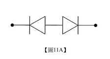
圖11A說明根據本揭露之一或多個實施例之等效電路。FIG. 11A illustrates an equivalent circuit according to one or more embodiments of the present disclosure.
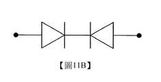
圖11B說明根據本揭露之一或多個實施例之等效電路。FIG. 11B illustrates an equivalent circuit according to one or more embodiments of the present disclosure.
圖12至圖18為根據本揭露之一或多個實施例製造半導體裝置的各個操作中之一者處的示意圖。12 to 18 are schematic diagrams of one of the operations of manufacturing a semiconductor device according to one or more embodiments of the present disclosure.
圖19為根據本揭露之一或多個實施例的半導體裝置的示意圖。FIG. 19 is a schematic diagram of a semiconductor device according to one or more embodiments of the present disclosure.
圖20為根據本揭露之一或多個實施例的半導體裝置的示意圖。FIG. 20 is a schematic diagram of a semiconductor device according to one or more embodiments of the present disclosure.
圖21A說明根據本揭露之一或多個實施例之等效電路。FIG. 21A illustrates an equivalent circuit according to one or more embodiments of the present disclosure.
圖21B說明根據本揭露之一或多個實施例之等效電路。FIG. 21B illustrates an equivalent circuit according to one or more embodiments of the present disclosure.
圖22為根據本揭露之一或多個實施例的半導體裝置的示意圖。FIG. 22 is a schematic diagram of a semiconductor device according to one or more embodiments of the present disclosure.
圖23為模擬結果,其說明Isoff與對應於隔離區之虛設閘極線之寬度之間的關係。FIG. 23 is a simulation result, which illustrates the relationship between Isoff and the width of the dummy gate line corresponding to the isolation region.
以下揭露內容提供用於實施所提供之標的物之不同特徵的許多不同實施例或實例。下文描述元件及配置之特定實例以簡化本揭露。當然,此等僅為實例且不意欲為限制性的。舉例而言,在以下描述中,第一特徵在第二特徵上方或上之形成可包括第一特徵與第二特徵直接接觸地形成之實施例,且亦可包括額外特徵可在第一特徵與第二特徵之間形成,使得第一特徵與第二特徵可能不直接接觸之實施例。另外,本揭露可在各種實例中重複參考數字及/或字母。此重複係出於簡單及清晰之目的,且本身並不指示所論述之各種實施例與/或組態之間的關係。The following disclosure provides many different embodiments or examples for implementing different features of the provided subject matter. Specific examples of components and configurations are described below to simplify the disclosure. Of course, these are only examples and are not intended to be limiting. For example, in the following description, the formation of the first feature on or on the second feature may include an embodiment in which the first feature and the second feature are formed in direct contact, and may also include additional features that may be formed between the first feature and the second feature. An embodiment is formed between the second feature so that the first feature and the second feature may not directly contact each other. In addition, the present disclosure may repeat reference numbers and/or letters in various examples. This repetition is for simplicity and clarity, and does not in itself indicate the relationship between the various embodiments and/or configurations discussed.
另外,空間相對術語,諸如「下方」、「在以下」、「下部」、「在以上」、「上部」、「上」等等,可在本文中為便於描述而使用,以描述在圖式中所說明之一個元件或特徵相對另一(些)元件或特徵之關係。除諸圖中所描繪之定向以外,空間相對術語意欲涵蓋裝置在使用或操作中之不同定向。設備可以其他方式定向(旋轉90度或處於其他定向),且本文中所使用之空間相對描述詞同樣可相應地進行解釋。In addition, spatial relative terms, such as "below", "below", "lower", "above", "upper", "upper", etc., can be used in this text for the convenience of description, to describe in the schema The relationship between one element or feature described in the description with respect to another element or feature(s). In addition to the orientations depicted in the figures, the spatial relative terms are intended to cover different orientations of the device in use or operation. The device can be oriented in other ways (rotated by 90 degrees or in other orientations), and this articleThe space relative descriptors used in can also be explained accordingly.
如本文所使用,諸如「第一」、「第二」及「第三」之術語描述各種元件、組件、區、層及/或區段,此等元件、組件、區、層及/或區段不應受此等術語限制。此等術語可僅用以區分一個元件、組件、區、層或區段與另一元件、組件、區、層或區段。除非上下文清楚地指示,否則諸如「第一」、「第二」及「第三」之術語當在本文中使用時並不暗示順序或次序。As used herein, terms such as "first", "second" and "third" describe various elements, components, regions, layers and/or sections, and these elements, components, regions, layers and/or regions The paragraph should not be restricted by these terms. These terms can only be used to distinguish one element, component, region, layer or section from another element, component, region, layer or section. Unless the context clearly indicates, terms such as "first", "second" and "third" when used herein do not imply an order or order.
如本文中所使用,術語「大約」、「大體上」、「實質」及「約」用以描述且慮及較小變化。當與事件或情形結合使用時,該等術語可指其中事件或情形明確發生之情況以及其中事件或情形極近似於發生之情況。舉例而言,當結合數值使用時,該等術語可指小於或等於彼數值之±10%的變化範圍,諸如小於或等於±5%、小於或等於±4%、小於或等於±3%、小於或等於±2%、小於或等於±1%、小於或等於±0.5%、小於或等於±0.1%或小於或等於±0.05%。舉例而言,若兩個數值之間的差小於或等於該等值之平均值的±10%(諸如,小於或等於±5%、小於或等於±4%、小於或等於±3%、小於或等於±2%、小於或等於±1%、小於或等於±0.5%、小於或等於±0.1%或小於或等於±0.05%),則可認為該兩個數值「大體上」相同或相等。舉例而言,「大體上」平行可指相對於0°而言小於或等於±10°之角度變化範圍,諸如,小於或等於±5°、小於或等於±4°、小於或等於±3°、小於或等於±2°、小於或等於±1°、小於或等於±0.5°、小於或等於±0.1°或小於或等於±0.05°之角度變化範圍。舉例而言,「大體上」垂直可指相對於90°而言±10°之角度變化範圍,諸如,小於或等於±5°、小於或等於±4°、小於或等於±3°、小於或等於±2°、小於或等於±1°、小於或等於±0.5°、小於或等於±0.1°或者小於或等於±0.05°之角度變化範圍。As used herein, the terms "approximately", "substantially", "substantial" and "about" are used to describe and allow for minor variations. When used in conjunction with an event or situation, these terms can refer to a situation in which the event or situation clearly occurs and a situation in which the event or situation closely resembles the occurrence. For example, when used in conjunction with numerical values, these terms can refer to a range of variation less than or equal to ±10% of that value, such as less than or equal to ±5%, less than or equal to ±4%, less than or equal to ±3%, Less than or equal to ±2%, less than or equal to ±1%, less than or equal to ±0.5%, less than or equal to ±0.1%, or less than or equal to ±0.05%. For example, if the difference between two values is less than or equal to ±10% of the average of these values (such as less than or equal to ±5%, less than or equal to ±4%, less than or equal to ±3%, less than Or equal to ±2%, less than or equal to ±1%, less than or equal to ±0.5%, less than or equal to ±0.1%, or less than or equal to ±0.05%), the two values can be considered "substantially" the same or equal. For example, "substantially" parallel may refer to a range of angular variation less than or equal to ±10° relative to 0°, such as less than or equal to ±5°, less than or equal to ±4°, less than or equal to ±3° , Less than or equal to ±2°, less than or equal to ±1°, less than or equal to ±0.5°, less than or equal to ±0.1°, or less than or equal to ±0.05°. For example, "substantially" vertical can refer to a range of angle variation of ±10° relative to 90°, such as less than or equal to ±5°, less than or equal to ±4°, less than or equal to ±3°, less than or Equal to ±2°, less than or equal to ±1°, less thanOr equal to ±0.5°, less than or equal to ±0.1°, or less than or equal to the range of angle change of ±0.05°.
鰭片可藉由任何適合之方法圖案化。舉例而言,鰭片可使用一或多個微影製程,包括雙重圖案化或多重圖案化製程圖案化。一般而言,雙重圖案化或多重圖案化製程組合了微影及自對準製程,從而允許產生具有例如小於使用單個、直接微影製程原本可獲得的圖案之間距的圖案。舉例而言,在一個實施例中,犧牲層形成在基底上方且使用微影製程圖案化。間隔件使用自對準製程在圖案化犧牲層旁邊形成。隨後移除犧牲層,且剩餘間隔件隨後可用於圖案化鰭片。The fins can be patterned by any suitable method. For example, the fins can be patterned using one or more lithography processes, including double patterning or multiple patterning processes. Generally speaking, double patterning or multiple patterning processes combine lithography and self-alignment processes to allow the creation of patterns having, for example, smaller pattern spacing than would otherwise be obtained using a single, direct lithography process. For example, in one embodiment, the sacrificial layer is formed on the substrate and patterned using a lithography process. The spacers are formed next to the patterned sacrificial layer using a self-aligned process. The sacrificial layer is then removed, and the remaining spacers can then be used to pattern the fins.
在本揭露之一或多個實施例中,提供一半導體裝置,其包括在相鄰電晶體裝置的一對源極/汲極區之間的隔離區。該隔離區具有一摻雜類型,該摻雜類型與該等源極/汲極區之摻雜類型相反。該對源極/汲極區與該隔離區協作地形成以背對背方式相連的兩個二極體裝置。只要該二極體裝置之正節點與負節點之間的電壓差低於該二極體裝置之擊穿電壓,該等背對背連接之二極體裝置即能夠在相鄰電晶體裝置的源極/汲極區之間提供側向隔離。In one or more embodiments of the present disclosure, a semiconductor device is provided, which includes an isolation region between a pair of source/drain regions of adjacent transistor devices. The isolation region has a doping type, which is opposite to the doping type of the source/drain regions. The pair of source/drain regions and the isolation region cooperate to form two diode devices connected in a back-to-back manner. As long as the voltage difference between the positive node and the negative node of the diode device is lower than the breakdown voltage of the diode device, the back-to-back diode devices can be connected to the source/ Provide lateral isolation between the drain regions.
圖1為說明一種用於根據本揭露之一或多個實施例的各種態樣製造半導體裝置之方法的流程圖。方法100開始於操作110,其中接收一半導體基板。該半導體基板包括形成在其上的半導體層。該半導體層包括一主動區。方法100以操作120繼續,其中在主動區中形成複數個電晶體裝置之複數個源極/汲極區。方法100以操作130繼續,其中將隔離區插入於兩個相鄰電晶體裝置的兩個相鄰源極/汲極區之間,其中該隔離區與該兩個相鄰源極/汲極區協作地形成以背對背方式電連接的兩個二極體裝置。FIG. 1 is a flowchart illustrating a method for manufacturing a semiconductor device in various aspects according to one or more embodiments of the present disclosure. The
方法100僅係實例,且不意欲限制本揭露為超出技術方案中明確列舉之內容。可在方法100之前、期間及之後提供額外操作,且一些所描述之操作可被替換、消除或移動以用於該方法之其他實施例。The
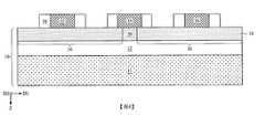
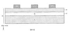
圖2至圖10為根據本揭露之一或多個實施例製造半導體裝置的各個操作中之一者處的示意圖,其中圖2至圖9為示意性橫截面圖,且圖10為示意性俯視圖。如圖2中所示,接收基板10。在一些實施例中,基板10可包括複合基板,諸如絕緣體上半導體(semiconductor-on-insulator;SOI)基板。藉助於實例,基板10可包括半導體基底11、在該半導體基底11上的絕緣層12,及在該絕緣層12上的半導體層14。該半導體基底11的材料可包含元素半導體,諸如矽或鍺;化合物半導體,諸如矽鍺、碳化矽、砷化鎵、磷化鎵、磷化銦或砷化銦;或其組合。絕緣層12可包括任何適合之絕緣材料。藉助於實例,絕緣層12可包括半導體氧化層,諸如氧化矽層,且組態為內埋氧化物。半導體層14可由與半導體基底11相同的材料形成,但不限於此。在一些實施例中,基板10為全空乏矽晶絕緣體(fully depleted silicon-on-insulator;FDSOI)基板。在某些替代實施例中,基板10可包括塊體半導體基板。FIGS. 2 to 10 are schematic diagrams of one of the operations of manufacturing a semiconductor device according to one or more embodiments of the present disclosure, wherein FIGS. 2 to 9 are schematic cross-sectional views, and FIG. 10 is a schematic top view . As shown in FIG. 2, the
如圖2中所展示,半導體層14之一部分可經摻雜,從而形成沿第一方向D1延伸之主動區16。主動區16具有第一摻雜類型。在一些實施例中,主動區16為由配置於第一方向D1中之多個電晶體裝置共用的共同主動區。由多個電晶體裝置共用的連續主動區經組態以保持應力,藉此增加裝置效能,尤其對於PMOS裝置。在一些實施例中,在主動區16中之電晶體裝置之間未插入諸如淺溝槽隔離的介電隔離。在一些實施例中,諸如STI的介電隔離可形成在主動區16中,但該介電隔離並不將主動區16劃分為分離的區,亦即,主動區16在介電隔離存在的情況下可仍然彼此連接。As shown in FIG. 2, a portion of the
如圖3中所展示,隔離區20形成於主動區16中。隔離區20為經摻雜區。在一些實施例中,隔離區20藉由離子植入形成於主動區16中。舉例而言,隔離區20可使用諸如光阻遮罩之圖案化遮罩層18植入於主動區16中。隔離區20可沿第二方向D2延伸。在一些實施例中,第二方向D2可大體上垂直於第一方向D1。在一些實施例中,主動區16與隔離區20可具有相同之第一摻雜類型。隔離區20的摻雜濃度高於主動區16的摻雜濃度。在一些實施例中,隔離區20的厚度大體上等於主動區16的厚度,但不限於此。As shown in FIG. 3, the
如圖4中所展示,圖案化遮罩層18可在隔離區20形成之後被移除。隨後,複數個閘極線形成於基板10上。在一些實施例中,第一閘極線32、第二閘極線34及第三閘極線36形成於半導體層14上。第一閘極線32、第二閘極線34及第三閘極線36可交替地配置在第一方向D1上,且第一閘極線32、第二閘極線34及第三閘極線36中之每一者可沿第二方向D2延伸。在一些實施例中,第二閘極線34沿垂直方向Z與隔離區20重疊。在一些實施例中,第一閘極線32、第二閘極線34及第三閘極線36為犧牲閘極線,且將在後續操作中移除。第一閘極線32、第二閘極線34及第三閘極線36可包括半導體閘極線,諸如多晶閘極線,但不限於此。在一些實施例中,隔離區20之尺寸可小於第二閘極線34之尺寸,但不限於此。As shown in FIG. 4, the patterned
在一些實施例中,側間隔件38可形成於第一閘極線32、第二閘極線34及第三閘極線36旁邊。側間隔件38的材料可包括諸如氧化矽的氧化物化合物、諸如氮化矽的氮化物化合物,其組合,或其他適合之介電材料。In some embodiments, the
如圖5中所展示,複數個源極/汲極區形成於基板10上。藉助於實例,一對第一源極/汲極區42形成於第一閘極線32旁邊,且一對第二源極/汲極區44形成於第三閘極線36旁邊。在一些實施例中,第一源極/汲極區42及第二源極/汲極區44可藉由在經由側間隔件38曝露之主動區16上磊晶生長半導體材料而形成。在一些實施例中,用於形成第一源極/汲極區42及第二源極/汲極區44的半導體材料不同於半導體層14的半導體材料。藉助於實例,用於形成第一源極/汲極區42及第二源極/汲極區44的半導體材料可包括矽鍺(SiGe)或其他適合之材料。在一些實施例中,摻雜物可連同第一源極/汲極區42及第二源極/汲極區44之形成而形成在第一源極/汲極區42及第二源極/汲極區44中。在一些其他實施例中,摻雜物可藉由植入操作形成。第一源極/汲極區42及第二源極/汲極區44可具有與隔離區20之第一摻雜類型相反之第二摻雜類型。藉助於實例,第一摻雜類型為P型,而第二摻雜類型為N型。As shown in FIG. 5, a plurality of source/drain regions are formed on the
在一些實施例中,可執行諸如退火操作之熱操作,以將第一源極/汲極區42及第二源極/汲極區44之摻雜物驅入主動區16中。在一些實施例中,第一源極/汲極區42及第二源極/汲極區44可將主動區16劃分為若干部分。舉例而言,主動區16的在該對第一源極/汲極區42之間及該對第二源極/汲極區44之間的部分組態為待形成的兩個相鄰電晶體裝置的兩個通道16C。主動區16的在第一源極/汲極區42與隔離區20之間及第二源極/汲極區44與隔離區20之間的部分組態為一對第二隔離區16D。因此,第二隔離區16D安置於隔離區20的兩個相對側上。隔離區20的摻雜濃度高於該對第二隔離區16D的摻雜濃度。在一些實施例中,隔離區20的厚度大體上等於通道16C的厚度,但不限於此。In some embodiments, a thermal operation such as an annealing operation may be performed to drive the dopants of the first source/
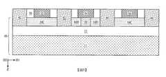
如圖6中所展示,第二閘極線34被移除。在一些實施例中,可形成圖案化遮罩層46,且經由圖案化遮罩層46曝露之第二閘極線34例如藉由蝕刻被移除,以形成曝露隔離區20之凹口47。在一些實施例中,凹口47之尺寸略微大於隔離區20尺寸,且凹口47可進一步但不限於曝露該對第二隔離區16D之一部分。As shown in FIG. 6, the
如圖7中所展示,圖案化遮罩層46被移除。在一些實施例中,介電層48形成於凹口47中,覆蓋隔離區20。介電層48可形成在基板10上,且凹口47外部之介電層48可例如藉由化學機械拋光(chemical mechanical polishing;CMP)或其類似者被移除。在一些實施例中,第一閘極線32及第三閘極線36被移除,以形成曝露通道16C之凹口50。As shown in Figure 7, the patterned
如圖8中所展示,閘極介電層52及諸如第一金屬閘極線54及第二金屬閘極線56的金屬閘極線形成於凹口50中。在一些實施例中,一或多個金屬層可形成於基板10上,且凹口50外部的一或多個金屬層可例如藉由化學機械拋光(CMP)或其類似者被移除,以形成第一金屬閘極線54及第二金屬閘極線56。As shown in FIG. 8, the
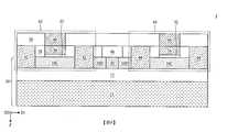
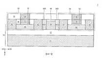
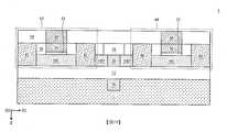
如圖9及圖l0中所展示,層間介電質(inter-layered dielectric;ILD)58形成於基板10上,且複數個接觸通孔60可形成於ILD58中且電連接至第一金屬閘極線54及第二金屬閘極線56,以形成半導體裝置1。在一些實施例中,第一金屬閘極線54的一部分組態為閘極電極54G,且閘極電極54G及安置於閘極電極54G的相對側上的一對第一源極/汲極區42形成第一電晶體裝置62。第二金屬閘極線56的一部分組態為閘極電極56G,且閘極電極56G及安置於閘極電極56G的相對側上的一對第二源極/汲極區44形成第二電晶體裝置64。As shown in FIGS. 9 and 10, an inter-layered dielectric (ILD) 58 is formed on the
參考圖9及圖10,半導體裝置1包括一對電晶體裝置,諸如形成在全空乏矽晶絕緣體(FDSOI)基板上的第一電晶體裝置62及第二電晶體裝置64。第一電晶體裝置62與第二電晶體裝置64共用相同主動區,且因此可改良佈局密度。形成在連續主動區(相同主動區16)中的第一電晶體裝置62的第一源極/汲極區42與第二電晶體裝置64的第二源極/汲極區44藉由隔離區20隔離。在一些實施例中,半導體基底11具有與隔離區20相同的摻雜類型,但不限於此。半導體基底11可為經摻雜基板,或可具有與隔離區具有相同摻雜類型的經摻雜井。半導體基底11具有相較於隔離區20較低的摻雜濃度。隔離區20具有與第一源極/汲極區42及第二源極/汲極區44的摻雜類型相反的摻雜類型。因此,第一源極/汲極區42、第二源極/汲極區44及隔離區20協作地形成以背對背方式電連接之兩個二極體裝置。9 and 10, the
背對背連接之二極體裝置能夠在第一電晶體裝置62的第一源極/汲極區42與第二電晶體裝置64的第二源極/汲極區44之間提供隔離,藉此減輕第一電晶體裝置62與第二電晶體裝置64之間的干擾。只要二極體裝置的陽極與陰極之間的電壓差低於該二極體裝置的擊穿電壓,隔離區20即能夠在第一電晶體裝置62的第一源極/汲極區42與第二電晶體裝置64的第二源極/汲極區44之間提供隔離。藉助於實例,當第一電晶體裝置62及第二電晶體裝置64為NMOS電晶體裝置時,第一源極/汲極區42及第二源極/汲極區44為N型,而隔離區20為P型。因此,如圖11A中所說明,兩個二極體裝置之陽極彼此電連接,而兩個二極體裝置之陰極分別電連接至第一電晶體裝置62的第一源極/汲極區42及第二電晶體裝置64的第二源極/汲極區44。當第一電晶體裝置62及第二電晶體裝置64為PMOS電晶體裝置時,第一源極/汲極區42及第二源極/汲極區44為P型,而隔離區20為N型。因此,如圖11B中所說明,兩個二極體裝置之陰極彼此電連接,而兩個二極體裝置之陽極分別電連接至第一電晶體裝置62的第一源極/汲極區42及第二電晶體裝置64的第二源極/汲極區44。The back-to-back diode device can provide isolation between the first source/
在一些實施例中,該對第二隔離區16D可被形成於隔離區20與第一源極/汲極區42之間及隔離區20與第二源極/汲極區44之間。該對第二隔離區16D與隔離區20具有相同摻雜類型,但相較於隔離區20具有較低摻雜濃度。隔離區20及第二隔離區16D具有與第一源極/汲極區42及第二源極/汲極區44之摻雜類型相反的摻雜類型。因此,第一源極/汲極區42、第二源極/汲極區44及隔離區20協作地形成以背對背方式電連接之兩個二極體裝置。只要二極體裝置的正節點與負節點之間的電壓差低於該二極體裝置的擊穿電壓,隔離區20即能夠在第一電晶體裝置62的第一源極/汲極區42與第二電晶體裝置64的第二源極/汲極區44之間提供隔離。在一些實施例中,具有相同摻雜類型但較低摻雜濃度的第二隔離區16D可幫助減小隔離區20的洩漏。In some embodiments, the pair of
在半導體裝置1的製造期間(如圖4至圖6中所說明),因設計規則及微影考慮因素而形成與第一閘極線32及第三閘極線36等距隔開的第二閘極線34。由於隔離區20與第二閘極線34重疊,因此可省略用於容納隔離區20的額外佈局區。During the manufacturing of the semiconductor device 1 (as illustrated in FIGS. 4 to 6), the
本揭露之半導體裝置及其製造方法不限於上文所提及之實施例,且可具有其他不同實施例。為簡化描述且為了本揭露之各實施例之間的比較的便利性,以下實施例中之每一者中之相同組件藉由相同編號標記。為更易於比較實施例之間的差異,以下描述將詳述不同實施例之間的不類似性,且不冗餘地描述相同特徵。The semiconductor device and the manufacturing method thereof of the present disclosure are not limited to the above-mentioned embodiments, and may have other different embodiments. To simplify the description and for the convenience of comparison between the various embodiments of the present disclosure, the same components in each of the following embodiments are marked with the same numbers. To make it easier to compare the differences between the embodiments, the following description will detail the differences between the different embodimentsDissimilarities, and the same features are not redundantly described.
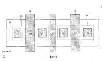
圖12至圖18為根據本揭露之一或多個實施例製造半導體裝置的各個操作中之一者處的示意圖,其中圖12至圖17為示意性橫截面圖,且圖18為示意性俯視圖。如圖12中所展示,接收基板10。在一些實施例中,基板10可為複合基板,諸如絕緣體上半導體(SOI)基板,其包括半導體基底11、在該半導體基底11上的絕緣層12,及在該絕緣層12上的半導體層14。半導體層14可經摻雜以形成具有第一摻雜類型之主動區16。隨後,複數個閘極線形成於基板10上。在一些實施例中,第一閘極線32、第二閘極線34及第三閘極線36形成於主動區16上。第一閘極線32、第二閘極線34及第三閘極線36可為犧牲閘極線,且將在後續操作中被移除。第一閘極線32、第二閘極線34及第三閘極線36可包括半導體閘極線,諸如多晶閘極線,但不限於此。FIGS. 12 to 18 are schematic diagrams of one of the operations of manufacturing a semiconductor device according to one or more embodiments of the present disclosure, wherein FIGS. 12 to 17 are schematic cross-sectional views, and FIG. 18 is a schematic top view . As shown in FIG. 12, the
如圖13中所展示,可在第一閘極線32、第二閘極線34及第三閘極線36旁邊形成複數個側間隔件38。複數個源極/汲極區亦形成於基板10上。藉助於實例,一對第一源極/汲極區域42形成於第一閘極線32旁邊,且一對第二源極/汲極區44形成於第三閘極線36旁邊。第一源極/汲極區42及第二源極/汲極區44可具有與隔離區20之第一摻雜類型相反之第二摻雜類型。As shown in FIG. 13, a plurality of
如圖14中所展示,第二閘極線34被移除。在一些實施例中,可形成圖案化遮罩層46,且經由圖案化遮罩層46曝露之第二閘極線34例如藉由蝕刻被移除,以形成部分地曝露主動區16的凹口47。As shown in FIG. 14, the
如圖15中所展示,半導體材料19可形成於圖案化遮罩層46上及凹口47的底部中。半導體材料19具有與第一源極/汲極區42及第二源極/汲極區44之第二摻雜類型相反之第一摻雜類型。形成於凹口47底部中的半導體材料19可經組態為隔離區20。在一些實施例中,隔離區20的尺寸可等於被移除的第二閘極線34的尺寸。As shown in FIG. 15, the
如圖16中所展示,可執行諸如退火操作之熱操作,以將第一源極/汲極區42及第二源極/汲極區44之摻雜物驅入主動區16中,且將隔離區20之摻雜物驅入主動區16中。在一些實施例中,隔離區20的厚度大於主動區16的厚度。半導體材料19可在熱操作之後連同圖案化遮罩層46一起被移除。在一些實施例中,介電層48形成於凹口47中,覆蓋隔離區20。介電層48可形成於基板10上,且凹口47外部之介電層48可例如藉由化學機械拋光(CMP)或其類似者被移除。As shown in FIG. 16, a thermal operation such as an annealing operation may be performed to drive the dopants of the first source/
在一些實施例中,第一源極/汲極區42、第二源極/汲極區44及隔離區20可將主動區16劃分為若干部分。舉例而言,主動區16的在該對第一源極/汲極區42之間及該對第二源極/汲極區44之間的部分組態為待形成的兩個相鄰電晶體裝置的兩個通道16C。隔離區20的厚度大於主動區16的厚度,但不限於此。主動區16的在第一源極/汲極區42與隔離區20之間及第二源極/汲極區44與隔離區20之間的部分組態為一對第二隔離區16D。因此,第二隔離區16D安置於隔離區20的兩個相對側上。隔離區20的摻雜濃度高於該對第二隔離區16D的摻雜濃度。In some embodiments, the first source/
如圖17及圖18中所展示,閘極介電層52、第一金屬閘極線54、第二金屬閘極線56、ILD 58,及複數個接觸通孔60可以與如圖8至圖10中所說明之類似方式形成,以形成半導體裝置2。As shown in FIGS. 17 and 18, the
參考圖17及圖18,隔離區20具有與第一源極/汲極區42及第二源極/汲極區44之摻雜類型相反的摻雜類型。因此,第一源極/汲極區42、第二源極/汲極區44及隔離區20協作地形成以背對背方式電連接之兩個二極體裝置。只要二極體裝置的正節點與負節點之間的電壓差低於該二極體裝置的擊穿電壓,隔離區20即能夠在第一電晶體裝置62的第一源極/汲極區42與第二電晶體裝置64的第二源極/汲極區44之間提供隔離。藉助於實例,當第一電晶體裝置62及第二電晶體裝置64為NMOS電晶體裝置時,第一源極/汲極區42及第二源極/汲極區44為N型,而隔離區20為P型。當第一電晶體裝置62及第二電晶體裝置64為PMOS電晶體裝置時,第一源極/汲極區42及第二源極/汲極區44為P型,而隔離區20為N型。Referring to FIGS. 17 and 18, the
在一些實施例中,該對第二隔離區16D可形成於隔離區20與第一源極/汲極區42之間及隔離區20與第二源極/汲極區44之間。第二隔離區16D與隔離區20具有相同摻雜類型,但相較於隔離區20具有較低摻雜濃度。隔離區20及第二隔離區16D具有與第一源極/汲極區42及第二源極/汲極區44之摻雜類型相反的摻雜類型,藉此形成兩個背對背連接之二極體裝置。只要二極體裝置的正節點與負節點之間的電壓差低於該二極體裝置的擊穿電壓,隔離區20即能夠在第一電晶體裝置62的第一源極/汲極區42與第二電晶體裝置64的第二源極/汲極區44之間提供隔離。In some embodiments, the pair of
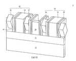
圖19為根據本揭露之一或多個實施例的半導體裝置的示意圖。如圖19中所展示,半導體裝置3可具有倒置井方案,其中該半導體基底11具有與隔離區20之摻雜類型相反的摻雜類型。半導體裝置3進一步包括在半導體基底11中之底部隔離區70。底部隔離區70具有與隔離區20相同的摻雜類型。在一些實施例中,隔離區20的摻雜濃度可大體上等於底部隔離區70的摻雜濃度。在一些實施例中,底部隔離區70大體上與隔離區20對準。底部隔離區70可鄰接絕緣層12。底部隔離區70可幫助增強第一電晶體裝置62之第一源極/汲極區42與第二電晶體裝置64之第二源極/汲極區44之間的隔離。在一些實施例中,半導體裝置3的其他組件可與如圖9中所展示之半導體裝置1的組件類似。在一些其他實施例中,半導體裝置3的其他組件可與如圖17中所展示的半導體裝置2的組件類似。FIG. 19 is a schematic diagram of a semiconductor device according to one or more embodiments of the present disclosure. As shown in FIG. 19, the
圖20為根據本揭露之一或多個實施例的半導體裝置的示意圖。如圖20中所展示,半導體裝置4的基板10為塊體半導體基板。基板10的材料可包含元素半導體,諸如矽或鍺;化合物半導體,諸如矽鍺、碳化矽、砷化鎵、磷化鎵、磷化銦或砷化銦;或其組合。半導體裝置4包括抗穿通層72,其在基板10與第一/第二電晶體裝置62/64之間及基板10與隔離區20之間。抗穿通層72可具有與隔離區20相同的摻雜類型。在一些實施例中,隔離區20的摻雜濃度大體上等於抗穿通層72的摻雜濃度,但不限於此。舉例而言,隔離區20的摻雜濃度可高於抗穿通層72的摻雜濃度。在一些實施例中,抗穿通層72與隔離區20可彼此接觸,且可電連接至參考電壓。抗穿通層72可經組態以減輕經由電流的穿通,而隔離區20可經組態以在第一電晶體裝置62/第二電晶體裝置64之間提供隔離。FIG. 20 is a schematic diagram of a semiconductor device according to one or more embodiments of the present disclosure. As shown in FIG. 20, the
當第一電晶體裝置62及第二電晶體裝置64為NMOS電晶體裝置時,第一源極/汲極區42及第二源極/汲極區44為N型,而隔離區20及抗穿通層72為P型。因此,如圖21A中所說明,兩個二極體裝置的陽極電連接至諸如接地電壓的參考電壓,而該兩個二極體裝置的陰極分別電連接至第一電晶體裝置62的第一源極/汲極區42及第二電晶體裝置64的第二源極/汲極區44。當第一電晶體裝置62及第二電晶體裝置64為PMOS電晶體裝置時,第一源極/汲極區42及第二源極/汲極區44為P型,而隔離區20及抗穿通層72為N型。因此,如圖21B中所說明,兩個二極體裝置的陰極電連接至諸如VDD的參考電壓,而該兩個二極體裝置的陽極分別電連接至第一電晶體裝置62的第一源極/汲極區42及第二電晶體裝置64的第二源極/汲極區44。When the
圖22為根據本揭露之一或多個實施例的半導體裝置的示意圖。如圖22中所展示,半導體裝置5的第一電晶體裝置62及第二電晶體裝置64可包括鰭式場效電晶體(fin field effect transistor;FinFET)電晶體。在一些實施例中,隔離區20安置於基板10與第一/第二電晶體裝置62/64之間。在一些實施例中,抗穿通層72的摻雜濃度可大體上等於隔離區20的摻雜濃度。在一些實施例中,抗穿通層72與隔離區20可彼此接觸,且可電連接至參考電壓。抗穿通層72可經組態以減輕經由電流的穿通,而隔離區20可經組態以在第一/第二電晶體裝置62/64之間提供隔離。FIG. 22 is a schematic diagram of a semiconductor device according to one or more embodiments of the present disclosure. As shown in FIG. 22, the
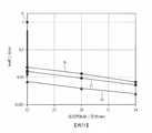
圖23為模擬結果,其說明Isoff與對應於隔離區之虛設閘極線之寬度之間的關係。樣本A表示在虛設閘極線下方未形成隔離區的半導體裝置。樣本B至D表示包括在虛設閘極線下方形成有具不同摻雜濃度之隔離區的半導體裝置,其中樣本C中之摻雜濃度低於樣本B中之摻雜濃度,且樣本D中之摻雜濃度低於樣本C中之摻雜濃度。如圖23中所展示,具有隔離區之半導體裝置(樣本B至D)相比於無隔離區之半導體裝置(樣本A)具有較低洩漏電流。FIG. 23 is a simulation result, which illustrates the relationship between Isoff and the width of the dummy gate line corresponding to the isolation region. Sample A represents a semiconductor device in which no isolation region is formed under the dummy gate line. Samples B to D represent semiconductor devices including isolation regions with different doping concentrations formed under the dummy gate lines, wherein the doping concentration in sample C is lower than that in sample B, and the doping concentration in sample D The impurity concentration is lower than the impurity concentration in sample C. As shown in FIG. 23, semiconductor devices with isolation regions (samples B to D) have lower leakage currents than semiconductor devices without isolation regions (sample A).
在本發明之一些實施例中,半導體裝置包括在相鄰電晶體裝置的源極/汲極區之間的隔離區。隔離區具有與源極/汲極區之摻雜類型相反之摻雜類型,藉此形成以背對背方式連接之兩個二極體裝置。只要該二極體裝置之正節點與負節點之間的電壓差低於該二極體裝置之擊穿電壓,該等背對背連接之二極體裝置即能夠在相鄰電晶體裝置的源極/汲極區之間提供側向隔離。隔離區可形成在與該等電晶體裝置的通道相同的主動區中,且因此可減小半導體裝置的製造成本及總高度。隔離區可形成於虛設閘極線下方,虛設閘極線因設計規則及微影考慮因素而形成,且將被移除。因此,可省略用於容納隔離區之額外佈局區。In some embodiments of the present invention, the semiconductor device includes an isolation region between the source/drain regions of adjacent transistor devices. The isolation region has a doping type opposite to the doping type of the source/drain regions, thereby forming two diode devices connected in a back-to-back manner. As long as the voltage difference between the positive node and the negative node of the diode device is lower than the breakdown voltage of the diode device, the back-to-back diode devices can be connected to the source/ Dip poleProvide lateral isolation between zones. The isolation region can be formed in the same active region as the channels of the transistor devices, and therefore the manufacturing cost and overall height of the semiconductor device can be reduced. The isolation region can be formed under the dummy gate line, which is formed due to design rules and lithography considerations, and will be removed. Therefore, the extra layout area for accommodating the isolation area can be omitted.
在一些實施例中,半導體裝置包括基板、一對電晶體裝置,及隔離區。該對電晶體裝置安置於該基板上。該對該等電晶體裝置中之每一者包括一通道、在該通道上方的一閘極電極,及在該閘極電極旁邊之一源極/汲極區。該隔離區在該對該等電晶體裝置之該等源極/汲極區之間。該隔離區具有一第一摻雜類型,該第一摻雜類型與該等源極/汲極區之一第二摻雜類型相反。In some embodiments, the semiconductor device includes a substrate, a pair of transistor devices, and an isolation region. The pair of transistor devices are arranged on the substrate. Each of the pair of transistor devices includes a channel, a gate electrode above the channel, and a source/drain region next to the gate electrode. The isolation region is between the source/drain regions of the pair of transistor devices. The isolation region has a first doping type, and the first doping type is opposite to the second doping type of one of the source/drain regions.
在一些實施例中,半導體裝置包括超過一個電晶體裝置,及隔離區。該等電晶體裝置配置為在共用主動區中彼此鄰接,在其間無介電隔離。該對該等電晶體裝置中之每一者包含一通道、在該通道上方的一閘極電極,及在該閘極電極之各別側上之一源極/汲極區。該隔離區係在該共同主動區中之該等電晶體裝置之間、插入於該等電晶體裝置之該等各別源極/汲極區之間。該隔離區包含一第一摻雜物類型,該第一摻雜物類型與該等電晶體裝置中該等源極/汲極區之一第二摻雜物類型相反。In some embodiments, the semiconductor device includes more than one transistor device and an isolation region. The transistor devices are configured to be adjacent to each other in the common active area without dielectric isolation therebetween. Each of the pair of transistor devices includes a channel, a gate electrode above the channel, and a source/drain region on each side of the gate electrode. The isolation region is between the transistor devices in the common active region and inserted between the respective source/drain regions of the transistor devices. The isolation region includes a first dopant type that is opposite to a second dopant type of one of the source/drain regions in the transistor devices.
在一些實施例中,提供一種製造半導體裝置的方法。接收包括一主動區之一基板。在該主動區中形成複數個電晶體裝置的複數個源極/汲極區。將一隔離區插入在兩個相鄰電晶體裝置的兩個相鄰源極/汲極區之間,其中該隔離區及該兩個相鄰源極/汲極區協作地形成以背對背方式電連接之兩個二極體裝置。In some embodiments, a method of manufacturing a semiconductor device is provided. Receiving a substrate including an active area. A plurality of source/drain regions of a plurality of transistor devices are formed in the active region. An isolation region is inserted between two adjacent source/drain regions of two adjacent transistor devices, wherein the isolation region and the two adjacent source/drain regions are cooperatively formed in a back-to-back manner. Two diode devices connected.
前文概述若干實施例之結構,使得熟習此項技術者可較佳地理解本揭露之態樣。熟習此項技術者應理解,其可易於使用本揭露作為設計或修改用於實現本文中所引入之實施例的相同目的及/或達成相同優點的其他方法及結構之依據。熟習此項技術者亦應認識到,此等等效構造並不脫離本揭露之精神及範疇,且熟習此項技術者可在不脫離本揭露之精神及範疇的情況下在本文中進行各種改變、替代及更改。The foregoing outlines the structure of several embodiments, so that those familiar with the technology can betterUnderstand the state of this disclosure. Those skilled in the art should understand that they can easily use the present disclosure as a basis for designing or modifying other methods and structures for achieving the same purpose and/or achieving the same advantages of the embodiments introduced herein. Those familiar with this technology should also realize that these equivalent structures do not depart from the spirit and scope of this disclosure, and those familiar with this technology can make various changes in this article without departing from the spirit and scope of this disclosure. , Substitution and modification.
1‧‧‧半導體裝置1‧‧‧Semiconductor device
10‧‧‧基板10‧‧‧Substrate
11‧‧‧半導體基底11‧‧‧Semiconductor substrate
12‧‧‧絕緣層12‧‧‧Insulation layer
16C‧‧‧通道16C‧‧‧Channel
16D‧‧‧第二隔離區16D‧‧‧Second quarantine area
20‧‧‧隔離區20‧‧‧Isolation Area
38‧‧‧側間隔件38‧‧‧Side spacer
42‧‧‧第一源極/汲極區42‧‧‧First source/drain region
44‧‧‧第二源極/汲極區44‧‧‧Second source/drain region
48‧‧‧介電層48‧‧‧Dielectric layer
52‧‧‧閘極介電層52‧‧‧Gate Dielectric Layer
54‧‧‧第一金屬閘極線54‧‧‧The first metal gate line
56‧‧‧第二金屬閘極線56‧‧‧Second metal gate line
58‧‧‧層間介電質58‧‧‧Interlayer dielectric
60‧‧‧接觸通孔60‧‧‧Contact through hole
62‧‧‧第一電晶體裝置62‧‧‧First Transistor Device
64‧‧‧第二電晶體裝置64‧‧‧Second Transistor Device
Claims (10)
Translated fromChineseApplications Claiming Priority (2)
| Application Number | Priority Date | Filing Date | Title |
|---|---|---|---|
| US15/939,876US10510776B2 (en) | 2018-03-29 | 2018-03-29 | Semiconductor device with common active area and method for manufacturing the same |
| US15/939,876 | 2018-03-29 |
Publications (2)
| Publication Number | Publication Date |
|---|---|
| TW201943073A TW201943073A (en) | 2019-11-01 |
| TWI725356Btrue TWI725356B (en) | 2021-04-21 |
Family
ID=68057175
Family Applications (1)
| Application Number | Title | Priority Date | Filing Date |
|---|---|---|---|
| TW107142130ATWI725356B (en) | 2018-03-29 | 2018-11-26 | Semiconductor device and method for manufacturing the same |
Country Status (3)
| Country | Link |
|---|---|
| US (2) | US10510776B2 (en) |
| CN (1) | CN110323219B (en) |
| TW (1) | TWI725356B (en) |
Families Citing this family (4)
| Publication number | Priority date | Publication date | Assignee | Title |
|---|---|---|---|---|
| US10388644B2 (en) | 2016-11-29 | 2019-08-20 | Taiwan Semiconductor Manufacturing Company, Ltd. | Method of manufacturing conductors and semiconductor device which includes conductors |
| US10510776B2 (en)* | 2018-03-29 | 2019-12-17 | Taiwan Semiconductor Manufacturing Company Ltd. | Semiconductor device with common active area and method for manufacturing the same |
| JP2021136379A (en)* | 2020-02-28 | 2021-09-13 | セイコーエプソン株式会社 | Non-volatile storage devices, semiconductor integrated circuit devices and electronic devices |
| KR20210152851A (en) | 2020-06-09 | 2021-12-16 | 삼성전자주식회사 | ESD(Electrostatic Discharge) device and ESD protection circuit comprising the same |
Citations (2)
| Publication number | Priority date | Publication date | Assignee | Title |
|---|---|---|---|---|
| US5485027A (en)* | 1988-11-08 | 1996-01-16 | Siliconix Incorporated | Isolated DMOS IC technology |
| US20140061737A1 (en)* | 2012-08-29 | 2014-03-06 | Taiwan Semiconductor Manufacturing Company, Ltd. | Isolation for Semiconductor Devices |
Family Cites Families (20)
| Publication number | Priority date | Publication date | Assignee | Title |
|---|---|---|---|---|
| JPH0831841A (en)* | 1994-07-12 | 1996-02-02 | Sony Corp | Semiconductor device and manufacturing method thereof |
| JPH1074843A (en)* | 1996-06-28 | 1998-03-17 | Toshiba Corp | Multi-power integrated circuit and multi-power integrated circuit system |
| CN1257556C (en)* | 2002-04-01 | 2006-05-24 | 华邦电子股份有限公司 | Masked ROM |
| US6900091B2 (en)* | 2002-08-14 | 2005-05-31 | Advanced Analogic Technologies, Inc. | Isolated complementary MOS devices in epi-less substrate |
| KR101374078B1 (en)* | 2007-06-04 | 2014-03-13 | 삼성디스플레이 주식회사 | Display substrate, method of manufacturing the same and display apparatus having the same |
| US8072015B2 (en) | 2007-06-04 | 2011-12-06 | Sony Corporation | Solid-state imaging device and manufacturing method thereof |
| US7939863B2 (en)* | 2008-08-07 | 2011-05-10 | Texas Instruments Incorporated | Area efficient 3D integration of low noise JFET and MOS in linear bipolar CMOS process |
| US9245805B2 (en) | 2009-09-24 | 2016-01-26 | Taiwan Semiconductor Manufacturing Company, Ltd. | Germanium FinFETs with metal gates and stressors |
| US8962400B2 (en) | 2011-07-07 | 2015-02-24 | Taiwan Semiconductor Manufacturing Company, Ltd. | In-situ doping of arsenic for source and drain epitaxy |
| US8841701B2 (en) | 2011-08-30 | 2014-09-23 | Taiwan Semiconductor Manufacturing Company, Ltd. | FinFET device having a channel defined in a diamond-like shape semiconductor structure |
| US9236267B2 (en) | 2012-02-09 | 2016-01-12 | Taiwan Semiconductor Manufacturing Company, Ltd. | Cut-mask patterning process for fin-like field effect transistor (FinFET) device |
| US8847293B2 (en) | 2012-03-02 | 2014-09-30 | Taiwan Semiconductor Manufacturing Company, Ltd. | Gate structure for semiconductor device |
| US8836016B2 (en) | 2012-03-08 | 2014-09-16 | Taiwan Semiconductor Manufacturing Company, Ltd. | Semiconductor structures and methods with high mobility and high energy bandgap materials |
| US8853025B2 (en) | 2013-02-08 | 2014-10-07 | Taiwan Semiconductor Manufacturing Company, Ltd. | FinFET/tri-gate channel doping for multiple threshold voltage tuning |
| US9093514B2 (en) | 2013-03-06 | 2015-07-28 | Taiwan Semiconductor Manufacturing Co., Ltd. | Strained and uniform doping technique for FINFETs |
| US9076863B2 (en)* | 2013-07-17 | 2015-07-07 | Texas Instruments Incorporated | Semiconductor structure with a doped region between two deep trench isolation structures |
| US9136106B2 (en) | 2013-12-19 | 2015-09-15 | Taiwan Semiconductor Manufacturing Company, Ltd. | Method for integrated circuit patterning |
| US9520482B1 (en) | 2015-11-13 | 2016-12-13 | Taiwan Semiconductor Manufacturing Company, Ltd. | Method of cutting metal gate |
| CN107248514B (en)* | 2017-06-06 | 2019-11-22 | 上海华力微电子有限公司 | A Novel ESD Protection Structure and Its Implementation Method |
| US10510776B2 (en)* | 2018-03-29 | 2019-12-17 | Taiwan Semiconductor Manufacturing Company Ltd. | Semiconductor device with common active area and method for manufacturing the same |
- 2018
- 2018-03-29USUS15/939,876patent/US10510776B2/enactiveActive
- 2018-11-26TWTW107142130Apatent/TWI725356B/enactive
- 2018-11-29CNCN201811440548.2Apatent/CN110323219B/enactiveActive
- 2019
- 2019-12-04USUS16/703,483patent/US11145678B2/enactiveActive
Patent Citations (2)
| Publication number | Priority date | Publication date | Assignee | Title |
|---|---|---|---|---|
| US5485027A (en)* | 1988-11-08 | 1996-01-16 | Siliconix Incorporated | Isolated DMOS IC technology |
| US20140061737A1 (en)* | 2012-08-29 | 2014-03-06 | Taiwan Semiconductor Manufacturing Company, Ltd. | Isolation for Semiconductor Devices |
Also Published As
| Publication number | Publication date |
|---|---|
| US11145678B2 (en) | 2021-10-12 |
| US10510776B2 (en) | 2019-12-17 |
| US20200105795A1 (en) | 2020-04-02 |
| TW201943073A (en) | 2019-11-01 |
| CN110323219B (en) | 2022-04-26 |
| CN110323219A (en) | 2019-10-11 |
| US20190305006A1 (en) | 2019-10-03 |
Similar Documents
| Publication | Publication Date | Title |
|---|---|---|
| US11424244B2 (en) | Integrated circuit having a vertical power MOS transistor | |
| US9053947B2 (en) | Methods for forming guard rings on fin structures | |
| JP5754881B2 (en) | New layout structure to improve performance | |
| TWI725356B (en) | Semiconductor device and method for manufacturing the same | |
| TWI488297B (en) | Component and its forming method | |
| JP5925740B2 (en) | Tunnel field effect transistor | |
| US9865505B2 (en) | Method for reducing N-type FinFET source and drain resistance | |
| CN108231864A (en) | Semiconductor device with a plurality of semiconductor chips | |
| US20220336261A1 (en) | Method of forming semiconductor device | |
| KR20140001087A (en) | Vertical power mosfet and methods of forming the same | |
| TWI768388B (en) | High voltage transistor with fin source/drain regions and trench gate structure | |
| TWI626678B (en) | High gain transistor for analog applications | |
| CN206584930U (en) | Integrated circuit | |
| CN106876393B (en) | Semiconductor device and method of forming the same | |
| TW201015715A (en) | Bipolar transistor and method for fabricating the same | |
| JP2009088449A (en) | Semiconductor device and manufacturing method thereof | |
| JP2016157970A (en) | Semiconductor device | |
| JP5926423B2 (en) | Semiconductor device | |
| JP2010177318A (en) | Semiconductor device and production method thereof | |
| JP2016048721A (en) | Semiconductor device and manufacturing method of the same |