TWI723019B - Techniques for forming transistors on the same die with varied channel materials - Google Patents
Techniques for forming transistors on the same die with varied channel materialsDownload PDFInfo
- Publication number
- TWI723019B TWI723019BTW105114006ATW105114006ATWI723019BTW I723019 BTWI723019 BTW I723019BTW 105114006 ATW105114006 ATW 105114006ATW 105114006 ATW105114006 ATW 105114006ATW I723019 BTWI723019 BTW I723019B
- Authority
- TW
- Taiwan
- Prior art keywords
- substrate
- fin
- semiconductor material
- transistor
- interface
- Prior art date
Links
- 239000000463materialSubstances0.000titleclaimsabstractdescription372
- 238000000034methodMethods0.000titleabstractdescription111
- 239000000758substrateSubstances0.000claimsabstractdescription160
- 229910000577Silicon-germaniumInorganic materials0.000claimsabstractdescription66
- 239000004065semiconductorSubstances0.000claimsdescription67
- XUIMIQQOPSSXEZ-UHFFFAOYSA-NSiliconChemical compound[Si]XUIMIQQOPSSXEZ-UHFFFAOYSA-N0.000claimsdescription49
- 229910052710siliconInorganic materials0.000claimsdescription49
- 239000010703siliconSubstances0.000claimsdescription49
- LEVVHYCKPQWKOP-UHFFFAOYSA-N[Si].[Ge]Chemical compound[Si].[Ge]LEVVHYCKPQWKOP-UHFFFAOYSA-N0.000claimsdescription48
- 230000007547defectEffects0.000claimsdescription45
- 229910052732germaniumInorganic materials0.000claimsdescription21
- GNPVGFCGXDBREM-UHFFFAOYSA-Ngermanium atomChemical compound[Ge]GNPVGFCGXDBREM-UHFFFAOYSA-N0.000claimsdescription21
- 239000002070nanowireSubstances0.000claimsdescription10
- 229910044991metal oxideInorganic materials0.000claimsdescription6
- 150000004706metal oxidesChemical class0.000claimsdescription6
- 230000000295complement effectEffects0.000claimsdescription4
- 230000005669field effectEffects0.000claimsdescription3
- 230000008901benefitEffects0.000abstractdescription7
- 230000006872improvementEffects0.000abstractdescription5
- 238000000151depositionMethods0.000description39
- 230000008021depositionEffects0.000description31
- 238000005530etchingMethods0.000description21
- 230000008569processEffects0.000description21
- 238000004891communicationMethods0.000description17
- 238000005516engineering processMethods0.000description16
- 238000002161passivationMethods0.000description15
- 239000010410layerSubstances0.000description13
- 229910000530Gallium indium arsenideInorganic materials0.000description11
- VYPSYNLAJGMNEJ-UHFFFAOYSA-NSilicium dioxideChemical compoundO=[Si]=OVYPSYNLAJGMNEJ-UHFFFAOYSA-N0.000description11
- KXNLCSXBJCPWGL-UHFFFAOYSA-N[Ga].[As].[In]Chemical compound[Ga].[As].[In]KXNLCSXBJCPWGL-UHFFFAOYSA-N0.000description11
- 230000015572biosynthetic processEffects0.000description11
- GPXJNWSHGFTCBW-UHFFFAOYSA-NIndium phosphideChemical compound[In]#PGPXJNWSHGFTCBW-UHFFFAOYSA-N0.000description9
- RPQDHPTXJYYUPQ-UHFFFAOYSA-Nindium arsenideChemical compound[In]#[As]RPQDHPTXJYYUPQ-UHFFFAOYSA-N0.000description9
- 238000002955isolationMethods0.000description8
- 238000000059patterningMethods0.000description8
- JBRZTFJDHDCESZ-UHFFFAOYSA-NAsGaChemical compound[As]#[Ga]JBRZTFJDHDCESZ-UHFFFAOYSA-N0.000description7
- 229910000673Indium arsenideInorganic materials0.000description7
- 229910001218Gallium arsenideInorganic materials0.000description6
- 238000005229chemical vapour depositionMethods0.000description5
- 239000013078crystalSubstances0.000description5
- 230000006870functionEffects0.000description5
- 229910052751metalInorganic materials0.000description5
- 239000002184metalSubstances0.000description5
- 238000005240physical vapour depositionMethods0.000description5
- 235000012239silicon dioxideNutrition0.000description5
- 239000000377silicon dioxideSubstances0.000description5
- 238000000231atomic layer depositionMethods0.000description4
- 239000011810insulating materialSubstances0.000description4
- 239000012212insulatorSubstances0.000description4
- 238000004943liquid phase epitaxyMethods0.000description4
- 125000006850spacer groupChemical group0.000description4
- -1InAlAsChemical compound0.000description3
- 229910052782aluminiumInorganic materials0.000description3
- XAGFODPZIPBFFR-UHFFFAOYSA-NaluminiumChemical compound[Al]XAGFODPZIPBFFR-UHFFFAOYSA-N0.000description3
- 238000000137annealingMethods0.000description3
- 150000001875compoundsChemical class0.000description3
- 238000005137deposition processMethods0.000description3
- 239000003989dielectric materialSubstances0.000description3
- 239000002019doping agentSubstances0.000description3
- 229910000449hafnium oxideInorganic materials0.000description3
- WIHZLLGSGQNAGK-UHFFFAOYSA-Nhafnium(4+);oxygen(2-)Chemical compound[O-2].[O-2].[Hf+4]WIHZLLGSGQNAGK-UHFFFAOYSA-N0.000description3
- 238000001451molecular beam epitaxyMethods0.000description3
- TWNQGVIAIRXVLR-UHFFFAOYSA-Noxo(oxoalumanyloxy)alumaneChemical compoundO=[Al]O[Al]=OTWNQGVIAIRXVLR-UHFFFAOYSA-N0.000description3
- 238000012545processingMethods0.000description3
- 239000010936titaniumSubstances0.000description3
- GWEVSGVZZGPLCZ-UHFFFAOYSA-NTitan oxideChemical compoundO=[Ti]=OGWEVSGVZZGPLCZ-UHFFFAOYSA-N0.000description2
- RTAQQCXQSZGOHL-UHFFFAOYSA-NTitaniumChemical compound[Ti]RTAQQCXQSZGOHL-UHFFFAOYSA-N0.000description2
- NRTOMJZYCJJWKI-UHFFFAOYSA-NTitanium nitrideChemical compound[Ti]#NNRTOMJZYCJJWKI-UHFFFAOYSA-N0.000description2
- MDPILPRLPQYEEN-UHFFFAOYSA-Naluminium arsenideChemical compound[As]#[Al]MDPILPRLPQYEEN-UHFFFAOYSA-N0.000description2
- 238000005280amorphizationMethods0.000description2
- 239000000969carrierSubstances0.000description2
- 239000010949copperSubstances0.000description2
- 238000013461designMethods0.000description2
- 238000001312dry etchingMethods0.000description2
- 238000011065in-situ storageMethods0.000description2
- MRELNEQAGSRDBK-UHFFFAOYSA-Nlanthanum(3+);oxygen(2-)Chemical compound[O-2].[O-2].[O-2].[La+3].[La+3]MRELNEQAGSRDBK-UHFFFAOYSA-N0.000description2
- 238000001459lithographyMethods0.000description2
- 238000004519manufacturing processMethods0.000description2
- 230000000873masking effectEffects0.000description2
- 239000000203mixtureSubstances0.000description2
- 239000002127nanobeltSubstances0.000description2
- 150000004767nitridesChemical class0.000description2
- SIWVEOZUMHYXCS-UHFFFAOYSA-Noxo(oxoyttriooxy)yttriumChemical compoundO=[Y]O[Y]=OSIWVEOZUMHYXCS-UHFFFAOYSA-N0.000description2
- 229910021420polycrystalline siliconInorganic materials0.000description2
- 229920005591polysiliconPolymers0.000description2
- 239000011669seleniumSubstances0.000description2
- 229910052719titaniumInorganic materials0.000description2
- OGIDPMRJRNCKJF-UHFFFAOYSA-Ntitanium oxideInorganic materials[Ti]=OOGIDPMRJRNCKJF-UHFFFAOYSA-N0.000description2
- WFKWXMTUELFFGS-UHFFFAOYSA-NtungstenChemical compound[W]WFKWXMTUELFFGS-UHFFFAOYSA-N0.000description2
- 229910052721tungstenInorganic materials0.000description2
- 239000010937tungstenSubstances0.000description2
- 238000001039wet etchingMethods0.000description2
- ZOXJGFHDIHLPTG-UHFFFAOYSA-NBoronChemical compound[B]ZOXJGFHDIHLPTG-UHFFFAOYSA-N0.000description1
- OKTJSMMVPCPJKN-UHFFFAOYSA-NCarbonChemical compound[C]OKTJSMMVPCPJKN-UHFFFAOYSA-N0.000description1
- RYGMFSIKBFXOCR-UHFFFAOYSA-NCopperChemical compound[Cu]RYGMFSIKBFXOCR-UHFFFAOYSA-N0.000description1
- YZCKVEUIGOORGS-OUBTZVSYSA-NDeuteriumChemical compound[2H]YZCKVEUIGOORGS-OUBTZVSYSA-N0.000description1
- GYHNNYVSQQEPJS-UHFFFAOYSA-NGalliumChemical compound[Ga]GYHNNYVSQQEPJS-UHFFFAOYSA-N0.000description1
- UFHFLCQGNIYNRP-UHFFFAOYSA-NHydrogenChemical compound[H][H]UFHFLCQGNIYNRP-UHFFFAOYSA-N0.000description1
- BUGBHKTXTAQXES-UHFFFAOYSA-NSeleniumChemical compound[Se]BUGBHKTXTAQXES-UHFFFAOYSA-N0.000description1
- 229910052581Si3N4Inorganic materials0.000description1
- 229910004298SiO 2Inorganic materials0.000description1
- BQCADISMDOOEFD-UHFFFAOYSA-NSilverChemical compound[Ag]BQCADISMDOOEFD-UHFFFAOYSA-N0.000description1
- NINIDFKCEFEMDL-UHFFFAOYSA-NSulfurChemical compound[S]NINIDFKCEFEMDL-UHFFFAOYSA-N0.000description1
- ATJFFYVFTNAWJD-UHFFFAOYSA-NTinChemical compound[Sn]ATJFFYVFTNAWJD-UHFFFAOYSA-N0.000description1
- XWCMFHPRATWWFO-UHFFFAOYSA-N[O-2].[Ta+5].[Sc+3].[O-2].[O-2].[O-2]Chemical compound[O-2].[Ta+5].[Sc+3].[O-2].[O-2].[O-2]XWCMFHPRATWWFO-UHFFFAOYSA-N0.000description1
- ILCYGSITMBHYNK-UHFFFAOYSA-N[Si]=O.[Hf]Chemical compound[Si]=O.[Hf]ILCYGSITMBHYNK-UHFFFAOYSA-N0.000description1
- NSXCBNDGHHHVKT-UHFFFAOYSA-N[Ti].[Sr].[Ba]Chemical compound[Ti].[Sr].[Ba]NSXCBNDGHHHVKT-UHFFFAOYSA-N0.000description1
- 229910045601alloyInorganic materials0.000description1
- 239000000956alloySubstances0.000description1
- AUCDRFABNLOFRE-UHFFFAOYSA-Nalumane;indiumChemical compound[AlH3].[In]AUCDRFABNLOFRE-UHFFFAOYSA-N0.000description1
- 238000004458analytical methodMethods0.000description1
- 238000004380ashingMethods0.000description1
- VKJLWXGJGDEGSO-UHFFFAOYSA-Nbarium(2+);oxygen(2-);titanium(4+)Chemical compound[O-2].[O-2].[O-2].[Ti+4].[Ba+2]VKJLWXGJGDEGSO-UHFFFAOYSA-N0.000description1
- 230000005540biological transmissionEffects0.000description1
- 229910052796boronInorganic materials0.000description1
- 239000003990capacitorSubstances0.000description1
- 229910052799carbonInorganic materials0.000description1
- 230000008859changeEffects0.000description1
- 238000003486chemical etchingMethods0.000description1
- 238000006243chemical reactionMethods0.000description1
- 229910052802copperInorganic materials0.000description1
- PMHQVHHXPFUNSP-UHFFFAOYSA-Mcopper(1+);methylsulfanylmethane;bromideChemical compoundBr[Cu].CSCPMHQVHHXPFUNSP-UHFFFAOYSA-M0.000description1
- 230000002950deficientEffects0.000description1
- 229910052805deuteriumInorganic materials0.000description1
- QYHNIMDZIYANJH-UHFFFAOYSA-NdiindiumChemical compound[In]#[In]QYHNIMDZIYANJH-UHFFFAOYSA-N0.000description1
- 230000005670electromagnetic radiationEffects0.000description1
- 238000011049fillingMethods0.000description1
- 229910052733galliumInorganic materials0.000description1
- PCHJSUWPFVWCPO-UHFFFAOYSA-NgoldChemical compound[Au]PCHJSUWPFVWCPO-UHFFFAOYSA-N0.000description1
- 229910052737goldInorganic materials0.000description1
- 239000010931goldSubstances0.000description1
- 238000010438heat treatmentMethods0.000description1
- 229910052738indiumInorganic materials0.000description1
- APFVFJFRJDLVQX-UHFFFAOYSA-Nindium atomChemical compound[In]APFVFJFRJDLVQX-UHFFFAOYSA-N0.000description1
- 238000010849ion bombardmentMethods0.000description1
- 238000005468ion implantationMethods0.000description1
- 230000001788irregularEffects0.000description1
- JQJCSZOEVBFDKO-UHFFFAOYSA-Nlead zincChemical compound[Zn].[Pb]JQJCSZOEVBFDKO-UHFFFAOYSA-N0.000description1
- 230000007774longtermEffects0.000description1
- 238000013507mappingMethods0.000description1
- 229910001092metal group alloyInorganic materials0.000description1
- 238000001465metallisationMethods0.000description1
- 150000002739metalsChemical class0.000description1
- 238000012986modificationMethods0.000description1
- 230000004048modificationEffects0.000description1
- 239000002074nanoribbonSubstances0.000description1
- 230000006911nucleationEffects0.000description1
- 238000010899nucleationMethods0.000description1
- 238000011017operating methodMethods0.000description1
- KJXBRHIPHIVJCS-UHFFFAOYSA-Noxo(oxoalumanyloxy)lanthanumChemical compoundO=[Al]O[La]=OKJXBRHIPHIVJCS-UHFFFAOYSA-N0.000description1
- BPUBBGLMJRNUCC-UHFFFAOYSA-Noxygen(2-);tantalum(5+)Chemical compound[O-2].[O-2].[O-2].[O-2].[O-2].[Ta+5].[Ta+5]BPUBBGLMJRNUCC-UHFFFAOYSA-N0.000description1
- RVTZCBVAJQQJTK-UHFFFAOYSA-Noxygen(2-);zirconium(4+)Chemical compound[O-2].[O-2].[Zr+4]RVTZCBVAJQQJTK-UHFFFAOYSA-N0.000description1
- 238000004626scanning electron microscopyMethods0.000description1
- 229910052711seleniumInorganic materials0.000description1
- HBMJWWWQQXIZIP-UHFFFAOYSA-Nsilicon carbideChemical compound[Si+]#[C-]HBMJWWWQQXIZIP-UHFFFAOYSA-N0.000description1
- 229910010271silicon carbideInorganic materials0.000description1
- HQVNEWCFYHHQES-UHFFFAOYSA-Nsilicon nitrideChemical compoundN12[Si]34N5[Si]62N3[Si]51N64HQVNEWCFYHHQES-UHFFFAOYSA-N0.000description1
- 229910052814silicon oxideInorganic materials0.000description1
- 229910052709silverInorganic materials0.000description1
- 239000004332silverSubstances0.000description1
- 239000002356single layerSubstances0.000description1
- 239000007787solidSubstances0.000description1
- 238000003860storageMethods0.000description1
- VEALVRVVWBQVSL-UHFFFAOYSA-Nstrontium titanateChemical compound[Sr+2].[O-][Ti]([O-])=OVEALVRVVWBQVSL-UHFFFAOYSA-N0.000description1
- 239000000126substanceSubstances0.000description1
- 238000006467substitution reactionMethods0.000description1
- 229910052717sulfurInorganic materials0.000description1
- 239000011593sulfurSubstances0.000description1
- 229910052715tantalumInorganic materials0.000description1
- GUVRBAGPIYLISA-UHFFFAOYSA-Ntantalum atomChemical compound[Ta]GUVRBAGPIYLISA-UHFFFAOYSA-N0.000description1
- MZLGASXMSKOWSE-UHFFFAOYSA-Ntantalum nitrideChemical compound[Ta]#NMZLGASXMSKOWSE-UHFFFAOYSA-N0.000description1
- 229910001936tantalum oxideInorganic materials0.000description1
- 229910052714telluriumInorganic materials0.000description1
- PORWMNRCUJJQNO-UHFFFAOYSA-Ntellurium atomChemical compound[Te]PORWMNRCUJJQNO-UHFFFAOYSA-N0.000description1
- 238000004627transmission electron microscopyMethods0.000description1
- 229910001928zirconium oxideInorganic materials0.000description1
- GFQYVLUOOAAOGM-UHFFFAOYSA-Nzirconium(iv) silicateChemical compound[Zr+4].[O-][Si]([O-])([O-])[O-]GFQYVLUOOAAOGM-UHFFFAOYSA-N0.000description1
Images


Classifications
- H—ELECTRICITY
- H10—SEMICONDUCTOR DEVICES; ELECTRIC SOLID-STATE DEVICES NOT OTHERWISE PROVIDED FOR
- H10D—INORGANIC ELECTRIC SEMICONDUCTOR DEVICES
- H10D30/00—Field-effect transistors [FET]
- H10D30/01—Manufacture or treatment
- H10D30/021—Manufacture or treatment of FETs having insulated gates [IGFET]
- H10D30/024—Manufacture or treatment of FETs having insulated gates [IGFET] of fin field-effect transistors [FinFET]
- H10D30/0243—Manufacture or treatment of FETs having insulated gates [IGFET] of fin field-effect transistors [FinFET] using dummy structures having essentially the same shapes as the semiconductor bodies, e.g. to provide stability
- H—ELECTRICITY
- H10—SEMICONDUCTOR DEVICES; ELECTRIC SOLID-STATE DEVICES NOT OTHERWISE PROVIDED FOR
- H10D—INORGANIC ELECTRIC SEMICONDUCTOR DEVICES
- H10D84/00—Integrated devices formed in or on semiconductor substrates that comprise only semiconducting layers, e.g. on Si wafers or on GaAs-on-Si wafers
- H10D84/80—Integrated devices formed in or on semiconductor substrates that comprise only semiconducting layers, e.g. on Si wafers or on GaAs-on-Si wafers characterised by the integration of at least one component covered by groups H10D12/00 or H10D30/00, e.g. integration of IGFETs
- H10D84/82—Integrated devices formed in or on semiconductor substrates that comprise only semiconducting layers, e.g. on Si wafers or on GaAs-on-Si wafers characterised by the integration of at least one component covered by groups H10D12/00 or H10D30/00, e.g. integration of IGFETs of only field-effect components
- H10D84/83—Integrated devices formed in or on semiconductor substrates that comprise only semiconducting layers, e.g. on Si wafers or on GaAs-on-Si wafers characterised by the integration of at least one component covered by groups H10D12/00 or H10D30/00, e.g. integration of IGFETs of only field-effect components of only insulated-gate FETs [IGFET]
- H10D84/85—Complementary IGFETs, e.g. CMOS
- H10D84/853—Complementary IGFETs, e.g. CMOS comprising FinFETs
- H—ELECTRICITY
- H01—ELECTRIC ELEMENTS
- H01L—SEMICONDUCTOR DEVICES NOT COVERED BY CLASS H10
- H01L21/00—Processes or apparatus adapted for the manufacture or treatment of semiconductor or solid state devices or of parts thereof
- H01L21/02—Manufacture or treatment of semiconductor devices or of parts thereof
- H01L21/02104—Forming layers
- H01L21/02365—Forming inorganic semiconducting materials on a substrate
- H01L21/02518—Deposited layers
- H01L21/02521—Materials
- H01L21/02524—Group 14 semiconducting materials
- H01L21/02532—Silicon, silicon germanium, germanium
- H—ELECTRICITY
- H01—ELECTRIC ELEMENTS
- H01L—SEMICONDUCTOR DEVICES NOT COVERED BY CLASS H10
- H01L21/00—Processes or apparatus adapted for the manufacture or treatment of semiconductor or solid state devices or of parts thereof
- H01L21/70—Manufacture or treatment of devices consisting of a plurality of solid state components formed in or on a common substrate or of parts thereof; Manufacture of integrated circuit devices or of parts thereof
- H01L21/71—Manufacture of specific parts of devices defined in group H01L21/70
- H01L21/76—Making of isolation regions between components
- H01L21/762—Dielectric regions, e.g. EPIC dielectric isolation, LOCOS; Trench refilling techniques, SOI technology, use of channel stoppers
- H01L21/76224—Dielectric regions, e.g. EPIC dielectric isolation, LOCOS; Trench refilling techniques, SOI technology, use of channel stoppers using trench refilling with dielectric materials
- H—ELECTRICITY
- H10—SEMICONDUCTOR DEVICES; ELECTRIC SOLID-STATE DEVICES NOT OTHERWISE PROVIDED FOR
- H10D—INORGANIC ELECTRIC SEMICONDUCTOR DEVICES
- H10D30/00—Field-effect transistors [FET]
- H10D30/60—Insulated-gate field-effect transistors [IGFET]
- H10D30/791—Arrangements for exerting mechanical stress on the crystal lattice of the channel regions
- H10D30/797—Arrangements for exerting mechanical stress on the crystal lattice of the channel regions being in source or drain regions, e.g. SiGe source or drain
- H—ELECTRICITY
- H10—SEMICONDUCTOR DEVICES; ELECTRIC SOLID-STATE DEVICES NOT OTHERWISE PROVIDED FOR
- H10D—INORGANIC ELECTRIC SEMICONDUCTOR DEVICES
- H10D62/00—Semiconductor bodies, or regions thereof, of devices having potential barriers
- H10D62/10—Shapes, relative sizes or dispositions of the regions of the semiconductor bodies; Shapes of the semiconductor bodies
- H10D62/13—Semiconductor regions connected to electrodes carrying current to be rectified, amplified or switched, e.g. source or drain regions
- H10D62/149—Source or drain regions of field-effect devices
- H10D62/151—Source or drain regions of field-effect devices of IGFETs
- H—ELECTRICITY
- H10—SEMICONDUCTOR DEVICES; ELECTRIC SOLID-STATE DEVICES NOT OTHERWISE PROVIDED FOR
- H10D—INORGANIC ELECTRIC SEMICONDUCTOR DEVICES
- H10D64/00—Electrodes of devices having potential barriers
- H10D64/01—Manufacture or treatment
- H10D64/017—Manufacture or treatment using dummy gates in processes wherein at least parts of the final gates are self-aligned to the dummy gates, i.e. replacement gate processes
- H—ELECTRICITY
- H10—SEMICONDUCTOR DEVICES; ELECTRIC SOLID-STATE DEVICES NOT OTHERWISE PROVIDED FOR
- H10D—INORGANIC ELECTRIC SEMICONDUCTOR DEVICES
- H10D84/00—Integrated devices formed in or on semiconductor substrates that comprise only semiconducting layers, e.g. on Si wafers or on GaAs-on-Si wafers
- H10D84/01—Manufacture or treatment
- H10D84/0123—Integrating together multiple components covered by H10D12/00 or H10D30/00, e.g. integrating multiple IGBTs
- H10D84/0126—Integrating together multiple components covered by H10D12/00 or H10D30/00, e.g. integrating multiple IGBTs the components including insulated gates, e.g. IGFETs
- H10D84/0165—Integrating together multiple components covered by H10D12/00 or H10D30/00, e.g. integrating multiple IGBTs the components including insulated gates, e.g. IGFETs the components including complementary IGFETs, e.g. CMOS devices
- H10D84/0167—Manufacturing their channels
- H—ELECTRICITY
- H10—SEMICONDUCTOR DEVICES; ELECTRIC SOLID-STATE DEVICES NOT OTHERWISE PROVIDED FOR
- H10D—INORGANIC ELECTRIC SEMICONDUCTOR DEVICES
- H10D84/00—Integrated devices formed in or on semiconductor substrates that comprise only semiconducting layers, e.g. on Si wafers or on GaAs-on-Si wafers
- H10D84/01—Manufacture or treatment
- H10D84/0123—Integrating together multiple components covered by H10D12/00 or H10D30/00, e.g. integrating multiple IGBTs
- H10D84/0126—Integrating together multiple components covered by H10D12/00 or H10D30/00, e.g. integrating multiple IGBTs the components including insulated gates, e.g. IGFETs
- H10D84/0165—Integrating together multiple components covered by H10D12/00 or H10D30/00, e.g. integrating multiple IGBTs the components including insulated gates, e.g. IGFETs the components including complementary IGFETs, e.g. CMOS devices
- H10D84/017—Manufacturing their source or drain regions, e.g. silicided source or drain regions
- H—ELECTRICITY
- H10—SEMICONDUCTOR DEVICES; ELECTRIC SOLID-STATE DEVICES NOT OTHERWISE PROVIDED FOR
- H10D—INORGANIC ELECTRIC SEMICONDUCTOR DEVICES
- H10D84/00—Integrated devices formed in or on semiconductor substrates that comprise only semiconducting layers, e.g. on Si wafers or on GaAs-on-Si wafers
- H10D84/01—Manufacture or treatment
- H10D84/0123—Integrating together multiple components covered by H10D12/00 or H10D30/00, e.g. integrating multiple IGBTs
- H10D84/0126—Integrating together multiple components covered by H10D12/00 or H10D30/00, e.g. integrating multiple IGBTs the components including insulated gates, e.g. IGFETs
- H10D84/0165—Integrating together multiple components covered by H10D12/00 or H10D30/00, e.g. integrating multiple IGBTs the components including insulated gates, e.g. IGFETs the components including complementary IGFETs, e.g. CMOS devices
- H10D84/0193—Integrating together multiple components covered by H10D12/00 or H10D30/00, e.g. integrating multiple IGBTs the components including insulated gates, e.g. IGFETs the components including complementary IGFETs, e.g. CMOS devices the components including FinFETs
- H—ELECTRICITY
- H10—SEMICONDUCTOR DEVICES; ELECTRIC SOLID-STATE DEVICES NOT OTHERWISE PROVIDED FOR
- H10D—INORGANIC ELECTRIC SEMICONDUCTOR DEVICES
- H10D84/00—Integrated devices formed in or on semiconductor substrates that comprise only semiconducting layers, e.g. on Si wafers or on GaAs-on-Si wafers
- H10D84/01—Manufacture or treatment
- H10D84/02—Manufacture or treatment characterised by using material-based technologies
- H10D84/03—Manufacture or treatment characterised by using material-based technologies using Group IV technology, e.g. silicon technology or silicon-carbide [SiC] technology
- H10D84/038—Manufacture or treatment characterised by using material-based technologies using Group IV technology, e.g. silicon technology or silicon-carbide [SiC] technology using silicon technology, e.g. SiGe
- H—ELECTRICITY
- H10—SEMICONDUCTOR DEVICES; ELECTRIC SOLID-STATE DEVICES NOT OTHERWISE PROVIDED FOR
- H10D—INORGANIC ELECTRIC SEMICONDUCTOR DEVICES
- H10D84/00—Integrated devices formed in or on semiconductor substrates that comprise only semiconducting layers, e.g. on Si wafers or on GaAs-on-Si wafers
- H10D84/01—Manufacture or treatment
- H10D84/02—Manufacture or treatment characterised by using material-based technologies
- H10D84/08—Manufacture or treatment characterised by using material-based technologies using combinations of technologies, e.g. using both Si and SiC technologies or using both Si and Group III-V technologies
- H—ELECTRICITY
- H10—SEMICONDUCTOR DEVICES; ELECTRIC SOLID-STATE DEVICES NOT OTHERWISE PROVIDED FOR
- H10D—INORGANIC ELECTRIC SEMICONDUCTOR DEVICES
- H10D84/00—Integrated devices formed in or on semiconductor substrates that comprise only semiconducting layers, e.g. on Si wafers or on GaAs-on-Si wafers
- H10D84/01—Manufacture or treatment
- H10D84/0123—Integrating together multiple components covered by H10D12/00 or H10D30/00, e.g. integrating multiple IGBTs
- H10D84/0126—Integrating together multiple components covered by H10D12/00 or H10D30/00, e.g. integrating multiple IGBTs the components including insulated gates, e.g. IGFETs
- H10D84/0165—Integrating together multiple components covered by H10D12/00 or H10D30/00, e.g. integrating multiple IGBTs the components including insulated gates, e.g. IGFETs the components including complementary IGFETs, e.g. CMOS devices
- H10D84/0188—Manufacturing their isolation regions
Landscapes
- Engineering & Computer Science (AREA)
- Physics & Mathematics (AREA)
- Condensed Matter Physics & Semiconductors (AREA)
- General Physics & Mathematics (AREA)
- Manufacturing & Machinery (AREA)
- Computer Hardware Design (AREA)
- Microelectronics & Electronic Packaging (AREA)
- Power Engineering (AREA)
- Insulated Gate Type Field-Effect Transistor (AREA)
- Metal-Oxide And Bipolar Metal-Oxide Semiconductor Integrated Circuits (AREA)
- Thin Film Transistor (AREA)
Abstract
Description
Translated fromChinese本發明係關於在具有不同通道材料的相同晶粒上形成電晶體之技術。The present invention relates to the technology of forming transistors on the same crystal grains with different channel materials.
基板上的電路裝置,包含電晶體、二極體、電阻器、電容器和形成在半導體基板上的其他被動和主動電子裝置的性能和良率的提高,通常是這些裝置的設計、製造和操作期間考慮的主要因素。例如,金屬氧化物半導體(MOS)電晶體半導體裝置,諸如那些用於互補金屬氧化物半導體(CMOS)裝置的設計和製造或形成期間,常常希望增加在n型MOS裝置(n-MOS)通道中的電子(載子)的移動,並且增加在p型MOS裝置(p-MOS)通道中的正電荷電洞(載子)的移動。對於電洞和電子多數載子MOS通道兩者,一般的CMOS電晶體裝置利用矽作為通道材料。The improvement of the performance and yield of circuit devices on the substrate, including transistors, diodes, resistors, capacitors, and other passive and active electronic devices formed on semiconductor substrates, is usually considered during the design, manufacturing and operation of these devices The main factor. For example, metal oxide semiconductor (MOS) transistor semiconductor devices, such as those used in the design and manufacture of complementary metal oxide semiconductor (CMOS) devices, or during formation, are often desired to be added to n-type MOS device (n-MOS) channels. The movement of electrons (carriers) and increase the movement of positive charge holes (carriers) in the p-MOS device (p-MOS) channel. For both hole and electron majority MOS channels, general CMOS transistor devices use silicon as the channel material.
100‧‧‧方法100‧‧‧Method
102‧‧‧沉積102‧‧‧Deposition
104‧‧‧蝕刻104‧‧‧Etching
106‧‧‧沉積106‧‧‧Deposition
108‧‧‧平坦化108‧‧‧Flattening
110‧‧‧重複110‧‧‧Repeat
112‧‧‧淺溝槽凹槽112‧‧‧Shallow groove groove
114‧‧‧沉積114‧‧‧Deposition
116‧‧‧鈍化116‧‧‧Passivation
118‧‧‧凹陷118‧‧‧Sag
120‧‧‧完成120‧‧‧Complete
200‧‧‧基板200‧‧‧Substrate
202‧‧‧本質基板材料鰭202‧‧‧essential substrate material fin
203‧‧‧通道區域203‧‧‧Access area
204‧‧‧本質基板材料鰭204‧‧‧essential substrate material fin
205‧‧‧通道區域205‧‧‧Access area
210‧‧‧硬掩模210‧‧‧Hard Mask
220‧‧‧溝槽220‧‧‧Groove
222‧‧‧溝槽222‧‧‧Groove
224‧‧‧溝槽224‧‧‧Groove
230‧‧‧第一替代材料230‧‧‧First alternative material
232‧‧‧第一替代材料鰭232‧‧‧The first alternative material fin
233‧‧‧通道區域233‧‧‧Access area
234‧‧‧第一替代材料鰭234‧‧‧The first alternative material fin
236‧‧‧第一替代材料鰭236‧‧‧The first alternative material fin
237‧‧‧通道區域237‧‧‧Access area
238‧‧‧第一替代材料鰭238‧‧‧The first alternative material fin
239‧‧‧通道區域239‧‧‧Access area
240‧‧‧第二替代材料區域240‧‧‧Second alternative material area
242‧‧‧第二替代材料鰭242‧‧‧The second alternative material fin
244‧‧‧第二替代材料鰭244‧‧‧The second alternative material fin
245‧‧‧通道區域245‧‧‧Access area
250‧‧‧STI材料250‧‧‧STI material
260‧‧‧閘極堆疊260‧‧‧Gate Stack
262‧‧‧閘極電極262‧‧‧Gate electrode
264‧‧‧間隔物264‧‧‧Spacer
266‧‧‧硬掩模266‧‧‧Hard Mask
303‧‧‧通道區域303‧‧‧Access area
305‧‧‧通道區域305‧‧‧Access area
333‧‧‧通道區域333‧‧‧Access area
335‧‧‧通道區域335‧‧‧Access area
337‧‧‧通道區域337‧‧‧Access area
339‧‧‧通道區域339‧‧‧Access area
343‧‧‧通道區域343‧‧‧Access area
345‧‧‧通道區域345‧‧‧Access area
402‧‧‧鰭402‧‧‧Fin
403‧‧‧通道區域403‧‧‧Access area
404‧‧‧鰭404‧‧‧Fin
405‧‧‧通道區域405‧‧‧Access area
432‧‧‧鰭432‧‧‧Fin
433‧‧‧通道區域433‧‧‧Access area
434‧‧‧鰭434‧‧‧Fin
435‧‧‧通道區域435‧‧‧Access area
436‧‧‧鰭436‧‧‧Fin
437‧‧‧通道區域437‧‧‧Access area
438‧‧‧鰭438‧‧‧Fin
439‧‧‧通道區域439‧‧‧Access area
442‧‧‧鰭442‧‧‧Fin
443‧‧‧通道區域443‧‧‧Access area
444‧‧‧鰭444‧‧‧Fin
445‧‧‧通道區域445‧‧‧Access area
1000‧‧‧計算系統1000‧‧‧Compute System
1002‧‧‧主機板1002‧‧‧Motherboard
1004‧‧‧處理器1004‧‧‧Processor
1006‧‧‧通訊晶片1006‧‧‧Communication chip
圖1顯示根據本揭露的各種實施例,形成積體電路的方法。FIG. 1 shows a method of forming an integrated circuit according to various embodiments of the present disclosure.
圖2A-K顯示根據本揭露的各種實施例,當實現圖1的方法時形成的範例性結構。2A-K show exemplary structures formed when the method of FIG. 1 is implemented according to various embodiments of the present disclosure.
圖3顯示根據本揭露的實施例,使用圖1的方法形成的積體電路。FIG. 3 shows an integrated circuit formed using the method of FIG. 1 according to an embodiment of the disclosure.
圖4顯示根據本揭露的實施例,在替代閘極程序期間,使用圖1的方法形成的積體電路。FIG. 4 shows an integrated circuit formed using the method of FIG. 1 during the replacement gate process according to an embodiment of the present disclosure.
圖5顯示根據本揭露的實施例,以使用在此揭露的技術形成的積體電路結構或裝置實現的計算系統。FIG. 5 shows a computing system implemented with an integrated circuit structure or device formed using the technology disclosed herein according to an embodiment of the disclosure.
在具有不同通道材料的相同晶粒上形成電晶體之技術被揭露。該技術包含在晶粒/基板上形成相對大的替代材料區域,接著在這些區域形成鰭。該鰭接著可用於形成電晶體通道區域,以及源極和汲極區域。在範例情況下,基板可以包含矽和替代材料,其可包含,例如,鍺、矽鍺和/或至少一種III-V族材料。替代材料區域可具有足以確保至少大部分的替代材料和基板材料之間的實質上平面的介面的寬度(例如,至少2倍寬於鰭的平均寬度)。因此,從替代材料區域形成的鰭也可以具有替代材料和基板材料之間的實質上平面的介面。一種範例性的好處為能夠以這樣實質上平面的介面來形成替代材料通道區域,其可以包含在固定的電壓流動的電流中至少30%的改善。許多變化和配置將因本揭露而顯而易見。The technology of forming transistors on the same crystal grains with different channel materials is disclosed. This technique involves forming relatively large areas of replacement material on the die/substrate, and then forming fins in these areas. This fin can then be used to form transistor channel regions, as well as source and drain regions. In an exemplary case, the substrate may include silicon and alternative materials, which may include, for example, germanium, silicon germanium, and/or at least one III-V group material. The substitute material area may have a width sufficient to ensure a substantially planar interface between at least most of the substitute material and the substrate material (for example, at least 2 times wider than the average width of the fin). Therefore, the fin formed from the alternative material region may also have a substantially planar interface between the alternative material and the substrate material. An exemplary benefit is that it is possible to form a channel area for alternative materials with such a substantially flat interface.Domain, which can contain at least a 30% improvement in the current flowing at a fixed voltage. Many changes and configurations will be apparent from this disclosure.
矽(Si)通常用作用於形成電路裝置,如電晶體的基板材料。在一些這樣的情況下,Si可專用於通道元件材料,如在n型和p型裝置兩者的金屬-氧化物-半導體(MOS)電晶體和隧道場效電晶體(FET)裝置中。而矽(Si)是相對常見的,廉價且充足的晶圓材料,其作為電晶體裝置的通道材料可能不提供最佳性能。因此,可能在一些應用中希望在同一基板上形成多個電晶體,其中該電晶體具有各種不同的通道材料。Silicon (Si) is commonly used as a substrate material for forming circuit devices such as transistors. In some such cases, Si may be dedicated to channel element materials, such as in metal-oxide-semiconductor (MOS) transistors and tunnel field-effect transistor (FET) devices in both n-type and p-type devices. Silicon (Si) is a relatively common, inexpensive and abundant wafer material, and its use as a channel material for transistor devices may not provide the best performance. Therefore, it may be desirable in some applications to form multiple transistors on the same substrate, where the transistors have various channel materials.
因此,並根據本揭露的一或多個實施例,揭露用於在具有不同通道材料的相同晶粒上形成電晶體之技術。該技術可使得材料的客制化組合被混合,並在單一本體晶粒或基板上匹配以最佳化每個裝置的活性載子極性的性能。在一些實施例中,例如,電晶體可以被形成在具有不同的通道區域的給定基板上,其中不同的通道區域包含下列中的至少兩種:Si、鍺(Ge)、矽鍺(SiGe)、和III-V族材料(例如,砷化銦鎵(InGaAs)、銦化銦(InP)、砷化銦(InAs)等)。例如,該技術可以被用於形成Si基板上的n-MOS Si通道和p-MOS SiGe通道裝置的組合,其中該n-MOS通道由原生於該基板的Si基板材料形成,並且該p-MOS通道由加在該基板的SiGe替代材料形成。在這樣的範例情況下,該Si基板的一或多個區域可以由適用於p-MOS裝置的SiGe材料構成的相對寬幅來代替。從該範例的情況下繼續,如果需要基於n-MOS裝置的III-V族材料,則n-MOS裝置可用包含至少一種III-V族材料的通道區域來形成,其中該Si基板的一或多個相對大區域由包含至少一種III-V族材料的區域替代。注意,根據最終用途或目標應用,用於一或多個電晶體的通道的本質矽區域可以或可以不保持。在一些實施例中,一或多個CMOS裝置可能由具有不同通道材料的該n-MOS和p-MOS裝置形成。Therefore, and according to one or more embodiments of the present disclosure, a technique for forming a transistor on the same crystal grain with different channel materials is disclosed. This technology allows customized combinations of materials to be mixed and matched on a single bulk die or substrate to optimize the performance of the active carrier polarity of each device. In some embodiments, for example, a transistor may be formed on a given substrate having different channel regions, where the different channel regions include at least two of the following: Si, germanium (Ge), silicon germanium (SiGe) , And III-V materials (for example, indium gallium arsenide (InGaAs), indium indium (InP), indium arsenide (InAs), etc.). For example, this technology can be used to form a combination of n-MOS Si channel and p-MOS SiGe channel device on a Si substrate, where the n-MOS channel is formed by Si substrate material native to the substrate, and the p-MOS The channel is replaced by SiGe added to the substrateMaterial formation. In such an exemplary case, one or more regions of the Si substrate can be replaced by a relatively wide SiGe material suitable for p-MOS devices. Continuing from the case of this example, if a III-V material based on an n-MOS device is required, the n-MOS device can be formed with a channel region containing at least one III-V material, wherein one or more of the Si substrate A relatively large area is replaced by an area containing at least one III-V group material. Note that depending on the end use or target application, the intrinsic silicon area of the channel used for one or more transistors may or may not be maintained. In some embodiments, one or more CMOS devices may be formed from the n-MOS and p-MOS devices with different channel materials.
本文所述的技術導致底層基板和替代材料之間的實質上平面的介面被形成,因而在替代材料之外形成鰭之前,在該基板中形成替代材料的相對寬區域。本文所用的實質上或幾乎或約為平面可以包含準確平面加或減與準確平面的5、10、15或20%變異,例如。因此,給定介面的每個最低和最高點將是在完美的或完全平坦的給定容差之內。更一般的意義來說,底層基板和替代材料之間的介面相較於藉由單一鰭替代程序形成的介面是較平坦的,其中定位鰭被蝕刻掉並且以其他材料代替。該寬的替代區域可以至少為1.5、2、3、4、5、10、20、50或100倍,或者提供底層基板和替代材料之間的平面的期望程度的一些其它適當的最小值。更一般的意義來說,替代材料的寬度比單一鰭寬度更寬,並且可以包含相當於雙排鰭、四排鰭或更多的尺寸。The techniques described herein result in the formation of a substantially planar interface between the underlying substrate and the replacement material, thus forming a relatively wide area of the replacement material in the substrate before the fins are formed outside the replacement material. The substantially or nearly or approximately plane used herein may include 5, 10, 15 or 20% variation of the exact plane plus or minus the exact plane, for example. Therefore, each lowest and highest point of a given interface will be within a given tolerance of perfect or completely flat. In a more general sense, the interface between the underlying substrate and the replacement material is flatter than the interface formed by a single fin replacement process, where the positioning fins are etched away and replaced with other materials. The wide replacement area may be at least 1.5, 2, 3, 4, 5, 10, 20, 50, or 100 times, or some other suitable minimum that provides the desired degree of flatness between the underlying substrate and the replacement material. In a more general sense, the width of the replacement material is wider than the width of a single fin, and can include dimensions equivalent to double-row fins, four-row fins or more.
從這樣較寬的區域形成鰭使得替代區域和底層基板之間的介面在至少大部分替代區域中為實質上平坦的,導致包含在替代材料和基板之間的實質上平坦介面的鰭。這可以比較,例如,形成於基板中的溝槽中的替代材料,藉由化學蝕刻形成的該溝槽成為所希望的鰭的寬度,其導致在替代材料和基板材料之間的刻面介面。這樣的刻面溝槽底部已被發現以抑制成核。將因本揭露而進一步理解,藉由物理蝕刻(例如,離子轟擊)形成的該溝槽也是不適合的,因為這樣的溝槽形成技術導致在溝槽底部的顯著非晶化和晶體損傷,其已被發現能抑制磊晶生長。因而,具有晶體損傷和/或非晶化的刻面溝槽底部和溝槽底部往往為替代材料提供不足的介面表面。這樣的溝槽底部往往在典型的溝槽形成程序中是固有的,特別是,其中溝槽為單一鰭結構的大小。為此,本揭露的技術避免非平坦或其他不良形成的溝槽底部。此外,一個鰭寬度的溝槽的底表面是難以清潔的,導致替代材料的沉積的起始表面相較於設置在使用本揭露的技術形成的溝槽中的起始表面為較低品質。例如,使用本揭露的技術形成的相對較寬的溝槽(例如,溝槽為在其中形成鰭的寬度的至少兩倍)是更容易清洗的,由此使得用於沉積替代材料的更高品質的起始表面(例如,至少在該鰭將在稍後形成的該部分)。Forming the fin from such a wide area makes the interface between the replacement area and the underlying substrate substantially flat in at least most of the replacement area, resulting in a fin containing a substantially flat interface between the replacement material and the substrate. This can be compared to, for example, a substitute material formed in a trench in the substrate, the trench formed by chemical etching becomes the width of the desired fin, which results in a faceted interface between the substitute material and the substrate material. Such faceted groove bottoms have been found to suppress nucleation. It will be further understood from the present disclosure that the trench formed by physical etching (for example, ion bombardment) is also unsuitable, because such trench formation technology causes significant amorphization and crystal damage at the bottom of the trench, which has been It was found to inhibit epitaxial growth. Therefore, faceted trench bottoms and trench bottoms with crystal damage and/or amorphization often provide insufficient interface surfaces for alternative materials. Such trench bottoms are often inherent in a typical trench formation process, especially where the trench is the size of a single fin structure. For this reason, the technology disclosed in the present disclosure avoids the bottom of the trench that is not flat or otherwise formed badly. In addition, the bottom surface of a trench with a fin width is difficult to clean, resulting in a lower quality of the starting surface of the deposition of the substitute material than the starting surface provided in the trench formed using the technology of the present disclosure. For example, relatively wide trenches formed using the disclosed technology (e.g., trenches that are at least twice the width of the fins formed therein) are easier to clean, thereby enabling higher quality for depositing alternative materials The starting surface (e.g., at least in the part where the fin will be formed later).
因此,替代區域和鰭在淺溝槽隔離(STI)之前形成,鈍化程序可用於幫助防止由隨後處理導致的問題,例如,防止由沉積STI材料導致的問題(或用不同的鰭材料增加該STI材料的相容性)。該技術可以被用於形成平面或非平面的(例如,鰭或奈米線/奈米帶)電晶體組態,如將因本揭露而顯而易見的。Therefore, replacement regions and fins are formed before shallow trench isolation (STI), passivation procedures can be used to help prevent problems caused by subsequent processing, for example, to prevent problems caused by depositing STI materials (or use differentThe fin material increases the compatibility of the STI material). This technique can be used to form planar or non-planar (for example, fins or nanowires/nanostrips) transistor configurations, as will be apparent from this disclosure.
在分析時(例如,使用掃描/透射電子顯微鏡(SEM/TEM)和/或組合物映射),根據一或多個實施例配置的結構或裝置將有效地顯示具有多個電晶體的基板,這種電晶體包含不同的通道材料。在一些情況下,晶粒或基板可以包含具有包含至少下列材料中的至少兩個:矽、鍺、矽鍺和III-V族材料的通道區域的電晶體。例如,基板可以是本體矽基板,並且形成在基板上的電晶體的替代通道可以包含矽鍺和至少一種III-V族材料(例如,砷化銦鎵、磷化銦、砷化銦等),其中形成的電晶體可能或可能不具有由矽基板材料形成的本質矽通道。因此,通道區域可以從和/或在該基板材料上形成。在一些情況下,該技術可以藉由觀察在電晶體的替代通道區域的替代材料和底層基板材料之間的介面進行檢測。本文所描述的各種技術可提供各種好處,包含能夠在單一晶粒或者基板上形成多個電晶體,其中該電晶體包含不同的通道材料,使得第一電晶體可以包括包含第一半導體材料的通道區域,並且第二電晶體可以包括包含第二半導體材料的通道區域。另一個好處,在一些實施例中,可以是電晶體性能的改善,諸如改善的電流流動(例如,在固定的電壓,大於10、20、30、40、或50%的電流流動改善)。這樣的好處可以被實現,因而通道替代材料和替代材料形成在其上的底層基板材料之間的實質上平面的介面。由於鰭被形成的替代材料的相對較寬的區域,實質上平面的介面是可以實現的,其中在相對較寬的區域沉積替代材料可以進行在更平坦的和更乾淨的起始表面。眾多的配置和變化將因本揭露而顯而易見。During analysis (for example, using scanning/transmission electron microscopy (SEM/TEM) and/or composition mapping), a structure or device configured according to one or more embodiments will effectively display a substrate with multiple transistors. This kind of transistor contains different channel materials. In some cases, the die or the substrate may include a transistor having a channel region including at least two of the following materials: silicon, germanium, silicon germanium, and III-V group materials. For example, the substrate may be a bulk silicon substrate, and the substitution channel of the transistor formed on the substrate may include silicon germanium and at least one III-V group material (for example, indium gallium arsenide, indium phosphide, indium arsenide, etc.), The transistor formed therein may or may not have the intrinsic silicon channel formed by the silicon substrate material. Therefore, the channel region can be formed from and/or on the substrate material. In some cases, this technique can be detected by observing the interface between the substitute material in the substitute channel area of the transistor and the underlying substrate material. The various techniques described herein can provide various benefits, including the ability to form multiple transistors on a single die or substrate, where the transistors contain different channel materials so that the first transistor can include channels containing the first semiconductor material Region, and the second transistor may include a channel region containing a second semiconductor material. Another benefit, in some embodiments, may be an improvement in transistor performance, such as improved current flow (for example, at a fixed voltage, greater than 10, 20, 30, 40, or 50% improvement in current flow). Such benefits can be realized, so that the channel substitute material and the substrate on which the substitute material is formedA substantially flat interface between substrate materials. Due to the relatively wide area of the replacement material where the fin is formed, a substantially planar interface is possible, where the deposition of the replacement material in the relatively wide area can be performed on a flatter and cleaner starting surface. Numerous configurations and changes will be apparent from this disclosure.
圖1顯示根據本揭露的一或多個實施例,形成積體電路的方法100。圖2A-K顯示根據各種實施例,當實現圖1的方法100時,形成的範例性結構。儘管圖2A-K的結構在此主要描繪和描述在形成鰭式電晶體配置(例如,三閘極或finFET)的情境中,本揭露不必如此限制。例如這些技術可被用於形成平面的、雙閘極、鰭式和/或奈米線(或環繞式閘極或奈米帶)電晶體配置,或其他合適的配置,如將因為本揭露而顯而易見的。圖3顯示根據實施例,包含使用本文所描述的技術形成各種電晶體配置的積體電路。FIG. 1 shows a
如在圖1中可以看出,根據實施例,方法100包含在基板200上沉積102硬掩模210以形成在圖2A所示的範例中得到的結構。在一些實施例中,基板200可以是:本體基板,其包含,例如,矽、矽鍺和/或III-V族材料;絕緣體上X(XOI)結構,其中X包含矽、矽鍺、鍺和/或III-V族材料,並且絕緣體材料是氧化物材料或介電材料或某些其它電絕緣材料;或一些其它合適的多層結構,其中該頂層包含矽、矽鍺和/或III-V族材料。在基板200上的硬掩模210可使用任何合適的技術被沉積。例如,硬掩模210可以使用化學氣相沉積(CVD)、原子層沉積(ALD)、液相磊晶(LPE)、物理氣相沉積(PVD)、分子束磊晶(MBE)和/或任何其它合適的程序在基板200上被覆蓋沉積或生長以在基板200上形成硬掩模210。在一些情況下,在硬掩模210的沉積之前,將被沉積的基板200的表面可以被處理(例如,化學處理、熱處理等)。硬掩模210可以由任何合適的材料組成,例如,如各種氧化物或氮化物材料。僅舉幾例,具體的氧化物和氮化物材料可包含氧化矽、氧化鈦、氧化鉿、氧化鋁或氮化鈦。在一些情況下,硬掩模210的材料可以基於所使用的基板200的材料來選擇。As can be seen in FIG. 1, according to an embodiment, the
圖1的方法100繼續於蝕刻104第一子集的區域以形成第一子集的溝槽220、222,由此形成如圖2B中所示根據實施例所得的範例結構。蝕刻104以形成第一子集的溝槽220、222可包含任何適當的蝕刻技術,諸如包含以下的程序的技術,例如:旋抗蝕、暴露、顯影、蝕刻和灰化以產生溝槽220。注意,任何合適的技術可以被用於形成溝槽220、222,如各種微影技術和各種濕式和/或乾式蝕刻程序。在一些實施例中,蝕刻104可在原位/不中斷空氣下執行,而在其他實施例中,蝕刻104可以是異地執行。溝槽220、222可基於最終用途或目標應用,利用變化的寬度W來形成。例如,溝槽220、222可利用大於單一鰭的寬度、大於雙列鰭的寬度、大於四列鰭的寬度等的寬度W來形成。因此,溝槽220、222(以及因此產生的替代區域)可形成為至少1.5、2、3、4、5、10、20、50或100倍,或比鰭形成的平均寬度更寬的一些其它合適的最小值。更具體地,溝槽220、222可被形成為大於10、20、40、60、100、200或500奈米,或者一些其它合適的最小寬度,例如,取決於最終用途或目標應用。在一些實施例中,溝槽寬度W可藉由操作的程序節點(例如,3奈米節點、5奈米節點、7奈米節點、10奈米節點等)和/或對於所得到的結構所需的鰭寬度/間距/數量來確定。在一些實施例中,溝槽222可形成為與溝槽220的寬度具有相同或不同的寬度。注意,雖然在圖2B的結構中顯示兩個溝槽220、222,任何數量的溝槽可以被形成,包含只有一個溝槽或多個溝槽,取決於最終用途或目標應用。The
圖1的方法100繼續於沉積106第一替代材料230在第一子集的溝槽220、222中以形成圖2C中所示根據實施例所得的範例結構。圖1的方法100繼續於平坦化108圖2C的結構以根據範例實施例形成圖2D的結構。在一些實施例中,第一替代材料230的沉積106可包含本文描述的任何沉積程序(例如,CVD、ALD、LPE、PVD、MBE),或任何其他合適的沉積程序。如在圖2C中可以看到的,在此範例實施例中,沉積106是選擇性沉積程序,以使替代材料230僅保留在溝槽220、222(並且不保留在硬掩模210的材料上)。然而,沉積106程序不必是選擇性,並且非選擇性程序可能在某些情況下可以使用。沉積106的選擇性可基於被沉積/生長的材料之間的黏著係數和在其上完成沉積/生長的表面被確定。沉積106可包含替代材料230的恆定沉積,或者它可以包含漸變的或多層的沉積。換句話說,替代材料230可以是,例如,單一組合物、漸變的或多層的。此外,替代材料230可根據最終用途或目標應用被應變和/或摻雜。在此範例實施例中,平面化108圖2C的表面包含去除過量填充、去除粗糙,並去除硬掩模材料210以形成圖2D所示的結構。The
在一些實施例中,第一替代材料230可包含,例如,矽,矽鍺和/或一或多個III-V族材料。在範例實施例中,基板200可以包含Si,並且替代材料230可以包含矽鍺。在這樣的範例實施例中,矽鍺可包含Si1-xGex,其中x的範圍可以從0.01至1(例如,0.2<X<0.8,以提供範例範圍)。因此,在一些實施例中,替代材料本身可包含100%的鍺或作為在矽鍺材料中的層(例如,如果矽鍺以漸變的方式被沉積)。在另一範例實施例中,基板200可包含Si,並且替代材料230可包含一或多個III-V族材料。範例III-V族材料包含砷化鎵(GaAs)、磷化銦(InP)、砷化銦(InAs)、砷化銦鎵(InGaAs)、砷化鋁(AlAs)、或砷化銦鋁(InAlAs)、或任何其它合適的III-V族材料。在一些實施例中,如果替代材料230包含一或多個III-V族替代材料,該材料可包含單層或包含多層疊堆的III-V族材料,如InP/InGaAs/InAs、GaAs/InP/InAs、GaAs/InGaAs/InAs、GaAs/InAlAs/InAs、InP/InGaAs/InP、GaAs/InAs、GaAs/InGaAs、或InP/InGaAs、或包含兩個或更多的III-V族材料的任何其它合適的多層疊堆。在一些這樣的實施例中,其中替代材料230是III-V族多層堆疊,高帶隙的III-V族材料可以在堆疊的底部附近使用(例如,以幫助減少對地的漏電流),例如,如GaAs、InP、InAlAs、或AlAs。此外,在一些這樣的實施例中,III-V族多層堆疊可以在堆疊的頂部附近採用低帶隙的III-V族材料(例如,以幫助形成到堆疊的接點),例如,諸如InAs或InGaAs。本文所討論的材料可以根據最終用途或目標應用被應變和/或摻雜。In some embodiments, the
在圖2D所示的範例結構中,基板200可包含矽,並且第一替代材料230可以包含矽鍺,以使有交替的本質矽區域和替代的矽鍺區域。在這樣的範例中,本質Si區域可以被使用以形成n-MOS裝置,並且矽鍺替代區域可以被使用以形成p-MOS裝置,接著該組合可以被用於形成CMOS裝置,如將因本揭露顯而易見的。在圖2D所示的範例結構中,基板200可包含矽鍺,並且第一替代材料230可包含一或多個III-V族材料,以使有交替的本質矽鍺區域和替代的III-V族材料區域。在這樣的範例中,本質矽鍺區域可以被使用以形成p-MOS裝置,並且III-V族替代區域可以被使用以形成n-MOS裝置,接著該組合可以被用於形成CMOS裝置,如將因本揭露顯而易見的。這些材料的組合僅用於說明目的被提供,而不是意在以任何方式限制本揭露。許多其他的材料組合將因本揭露顯而易見的。In the exemplary structure shown in FIG. 2D, the
圖1的方法100選擇性地繼續於重複110本文描述得程序102~108以建立替代區域的N個子集。根據範例實施例,圖2E顯示重複110程序102~108(例如,掩模、蝕刻、沉積、平坦化)一次,以形成第二替代材料區域240。雖然為了便於說明,區域230和240的深度D在本範例情況下被顯示為相同,它們不必具有相同的深度。例如,在其他情況下,蝕刻程序104可被執行以建立用於隨後替代材料區域的較深或較淺的溝槽。更具體地,在此範例的情況下,替代區域240的溝槽可已被形成為1.1、1.2、1.5、2、2.5、3、4、5或10倍,或一些其它合適的相對量,相對於溝槽220、222對於替代區域230形成更深或較淺,這將導致區域240的深度D在沉積106和平坦化108程序執行之後相對較深或較淺。每個替代材料區域的不同深度D可以被選擇以適應子鰭電流洩漏控制方法,例如,如子鰭轉換為絕緣體或子鰭摻雜。對於替代材料區域選擇不同的深度D的其它好處將因本揭露顯而易見。請注意,如果程序102~108被重複110多次以形成替代區域的N個子集,替代溝槽可以包含每個替代區域的子集的最終所需深度的額外深度以允許在平面化108程序期間去除材料和/或以確保每個替代區域的子集足夠的最後區域深度D。The
繼續於圖2E,該第二替代材料240可以包含如先前參考第一替代材料230描述的任何材料。例如,第二替代材料240可以包含矽、矽鍺,和/或一或多個III-V族材料。在範例實施例中,基板200包含矽,第一替代材料230包含矽鍺或一或多個III-V族材料中的一者,並且第二替代材料240包含矽鍺和一或多個III-V族材料中的另一者(相對於第一替代材料230包含的)。在這樣的範例實施例中,第一替代材料230可以包含矽鍺,並且第二替代材料240可包含一或多個III-V族材料。在一些實施例中,替代區域240可以包含與替代區域230相同的材料,並且不同子集的區域可以被形成以實現,例如,包含相同材料但不同的深度的區域,其取決於最終用途或目標應用。回想程序102~108可根據需要很多次數被重複110,以形成具有N個子集的替代區域。Continuing with FIG. 2E, the second
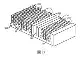
根據實施例,圖1的方法100繼續於用於隔離的淺溝槽凹槽112以圖案化在圖2E的結構中的鰭(202、232、242),並由此形成圖2F的所得範例結構。淺溝槽凹槽112可包含任何數目的掩模和蝕刻程序,和/或任何其它合適的技術,如標準微影或主鏈或間隔物方法。在範例情況下,圖2F的結構的所有的鰭(202、232、242)可能已被圖案化,並使用一個隔離溝槽蝕刻程序被形成,而在其他情況下,可能已使用多個隔離溝槽蝕刻程序。注意,蝕刻104可用於蝕刻在基板中將稍後由替代半導體材料所填充的一或多個相對較寬的溝槽(例如,圖2B中所示的溝槽220和222)(例如,沉積106期間),而淺溝槽凹槽112係用來蝕刻在替代材料區域中的溝槽(例如,圖2F中所示的溝槽224)以及,當存在時,將稍後由絕緣材料所填充,用於隔離形成在所得結構中的鰭的本質基板材料區域。因此,蝕刻112可被執行以建立用於形成在替代材料區域中的所得鰭的隔離溝槽以及,當存在時,本質基板材料區域,其中,該鰭實質上是反溝槽。當使用淺溝槽凹槽程序112來圖案化鰭時,基於使用的程序,每個鰭的所得鰭寬度FW和鰭間距FP可以依需要被實現。在一些實施例中,隔離溝槽蝕刻所得形成的所有所得鰭可以具有相同或相似的鰭寬度FW和/或鰭間距FP,而在其他實施例中,鰭可以具有不同的鰭寬度FW和/或鰭間距FP。請注意,在某些情況下,不同材料的區域可具有不同的蝕刻偏差並且因此可能需要不同的如繪製鰭寬度以實現相等的最終圖案化鰭寬度FW和/或鰭間距FP。進一步注意到,在圖案化112之前,用於區域的子集的深度D和寬度W可能影響在圖案化112之後形成的所得結構的鰭寬度FW、鰭間距FP和鰭高度。在一些實施例中,鰭寬度FW和鰭間距FP可以用任意的方式,或者為了滿足所需的最終用途或目標應用被形成。鰭尺寸、形狀、數量、間距和配置的許多變化將因本揭露而顯而易見。According to an embodiment, the
在圖2F中顯示的具體範例結構中,作為淺溝槽凹陷程序的結果,雙鰭202係以本質基板材料形成,四鰭232係以第一替代材料形成,並且雙鰭242係以第二替代材料形成。如也可以看出的,從替代材料區域230、240形成的鰭232、242包含在鰭的較低部分的本質基板材料的一部分;然而,鰭不必以這樣的方式被形成。在一些實施例中,形成的鰭可以包含單一材料(例如,只有矽、矽鍺或III-V族材料),或者其可以包含多種材料,如在圖2F所示的鰭232、242。在具體的範例的情況下,鰭202可包含矽(其中,基板200包含矽),第一替代材料鰭232可包含矽鍺,並且第二替代材料鰭242可包含一或多個III-V族材料。注意,雖然本質基板材料鰭202被顯示在圖2F的範例結構中,本文描述的技術可以被用來代替本質基板材料的整體,導致僅具有替代材料的鰭的結構。進一步注意到,儘管三種不同鰭類型(202、232、242)被顯示在圖2F的範例結構中,本文描述的技術可以用於提供任何數目的鰭類型。例如,在另一個實施例中,圖2F可以進一步理解為包含四條鰭類型:矽鰭202、鍺鰭232(兩個最接近於前景的鰭),矽鍺鰭232(顯示的另一組鰭232),和III-V族材料鰭242。這些鰭類型中的任何一種可以對於基板是本質的。另外,所有四種鰭類型可以是替代鰭。在任何情況下,這些鰭類型中的每一個可以被用以形成不同的電晶體類型。In the specific example structure shown in FIG. 2F, as a result of the shallow trench recessing process, the
如可從圖2F看出的,多個鰭係從圖2E的結構的區域形成。例如,第一替代區域230和第二材料替代區域240被圖案化112到兩個鰭中的每一個,如是230區域之間的本質基板材料區域,對於圖2F的結構中關注的總共八個鰭。從替代區域230、240和基板200上(不論基板材料是否為鰭的一部分)形成的鰭232、242具有替代材料和基板材料之間實質上為平面的介面。例如,在圖2F中的介面X(由虛線橢圓表示)顯示在鰭232中的替代材料230和基板材料之間的介面。實質上或幾乎平坦的介面(相對於曲面的或有刻面的或其他非平面介面)可以使用方法100來實現,因為從替代區域形成的鰭具有比從這樣的區域形成的鰭寬度FW更大的寬度W。換句話說,沉積替代材料成具有實質上或幾乎相同於從替代材料形成的窄鰭的寬度的溝槽,導致在溝槽底部難以形成平面介面。在此範例實施例中,因為溝槽222係以大於鰭232的鰭寬度FW的寬度W來形成(例如,特定情況來說,至少2倍以上),第一替代填充材料係沉積在實質上平面(或是平坦)的表面。此外,當在蝕刻104期間形成溝槽時(例如,溝槽220和222),用於溝槽底部的較高品質的起始表面可以被實現,由於,例如,在溝槽中的表面更容易被清除,結果係比一個鰭所需要的寬度更寬。例如,如本文所用的實質上或幾乎平坦的可以包含準確的平面從準確平面加或減5、10、15或20%的變化。本文所描述的技術和所得結構的許多其它好處將因本揭露而顯而易見。As can be seen from Fig. 2F, the multiple fin systems from the junction of Fig. 2EThe structured area is formed. For example, the
根據實施例,圖1的方法100繼續於沉積114淺溝槽隔離(STI)或其它絕緣材料250,接著進行平面化以形成圖2G的所得範例結構。STI材料250的沉積114可以包含本文描述的任何沉積程序(例如,CVD、ALD、LPE、PVD、MBE),或任何其他合適的沉積程序。STI材料250可包含任何合適的絕緣材料,諸如一或多個介電質或氧化物材料(例如,二氧化矽)。According to an embodiment, the
在一些實施例中,STI材料250的沉積可以包含可選的鈍化116程序,例如,用以防止由STI材料250的沉積造成的問題和/或增加STI材料250與變化鰭材料的相容性。這樣的鈍化程序116可以發生在沉積程序114之前、期間和/或之後(因此在相關的平坦化程序之前或之後)。在一些情況下,鈍化116程序可以取決於鰭材料和STI材料。例如,在二氧化矽用作STI材料250的情況下,當在矽鍺或鍺鰭上沉積二氧化矽STI材料時,氧化釔或氮化鋁可以使用作為鈍化材料。在另一範例情況下,二氧化矽被用作STI材料250時,當在包含一或多個III-V族材料的鰭上沉積二氧化矽STI材料,氧化鋁、氧化鉿或硫可以使用作為鈍化材料。在一些實施例中,鈍化可以對於STI材料250是本質的,而在其他實施例中,在鰭(202、232、242)之間的溝槽中沉積STI材料250之前,鈍化襯墊可被沉積/生長在鰭壁上。在實施例中,鈍化116被執行在STI材料250的沉積之後,這樣的程序可以包含,例如,高壓氫氣或氘退火。任何合適的鈍化技術和材料可被使用,如將因本揭露而顯而易見的。In some embodiments, the deposition of the
根據實施例,圖1的方法100選擇性地繼續於凹陷118 STI材料250以形成圖2H的範例所得結構。在實施例中,STI材料250不被凹陷,例如,所得的結構可以用於平面電晶體配置。在此範例實施例中,其中STI材料250被凹陷118以重新暴露鰭202、232和242,所得的結構可以被用於非平面電晶體配置,如將在本文更詳細描述的。凹陷118 STI材料250可包含任何合適的技術,例如,如掩模和蝕刻程序。如在圖2H的範例結構中可以看出,STI材料250被凹陷118到等於鰭232和242的替代材料的底部的程度(換句話說,到等於實質上平坦的介面X的程度)。在一些這樣的情況下,由於鰭232和242的STI材料250和替代材料之間沒有重疊,鈍化116可能不是需要的。然而,在一些情況中,STI材料250可以被凹陷118到其他程度,例如,如比X介面程度高。在一些這樣的情況下,鈍化116可用於幫助鰭232和242的STI材料250和替代材料之間的重疊。在一些實施例中,在凹陷118已經被完成之後,根據最終用途或目標應用,額外的鈍化程序可被執行。According to an embodiment, the
根據一些實施例,圖1的方法100選擇性地繼續於完成120一或多個電晶體的形成,以形成圖2I-K中的範例所得結構。根據實施例,如在圖2I中所示,各種不同的程序可被執行以完成120一或多個電晶體的形成,並且這樣的程序可包含形成閘極堆疊260於鰭202、232和242上。在一些實施例中,閘極堆疊260的形成可以包含虛設閘極氧化物沉積、虛設閘極電極(例如,多晶矽)沉積和圖案化硬掩模沉積。額外的處理可包含圖案化虛設閘極和沉積/刻蝕間隔材料。在這樣的程序之後,該方法可以繼續於絕緣體沉積、平坦化,接著虛設閘極電極和閘極氧化物去除以暴露電晶體的通道區域,例如用於替代金屬閘極(RMG)的程序就完成了。在打開通道區域之後,虛設閘極氧化物和電極可被分別代替,例如,高k介電質和替代金屬閘極。其他實施例可以包含藉由任何合適的程序形成標準的閘極堆疊。任何數量的標準後端程序也可以被進行,以幫助完成120一或多個電晶體的形成。方法100可包含各種合適的額外或替代程序,如將因本揭露顯而易見的。According to some embodiments, the
在圖2J中所示的範例結構中,閘極堆疊260包含閘極電極262和直接形成在閘極電極262下的閘極介電質(為了便於說明,未顯示)。閘極介電質和閘極電極可使用任何合適的技術和從任何合適的材料來形成。例如,如前面所述,在替代金屬閘極程序期間,閘極堆疊已被形成,並且這樣的程序可包含任何合適的沉積技術(例如,CVD、PVD等)。閘極介電質可以是,例如,任何合適的氧化物如SiO2或高k閘極介電質材料。高k閘極介電質材料的範例包含,例如,氧化鉿、氧化鉿矽、氧化鑭、氧化鑭鋁、氧化鋯、氧化鋯矽、氧化鉭、氧化鈦、氧化鋇鍶鈦、氧化鋇鈦、氧化鍶鈦、氧化釔、氧化鋁、氧化鉛鈧鉭和鈮酸鉛鋅。在一些實施例中,當使用高k材料時,可以在閘極介電層上進行退火程序以提高其品質。通常,閘極介電質的厚度應足以將閘極電極與源極和汲極接點電隔離。此外,閘極電極262可包含範圍廣的材料,諸如多晶矽、氮化矽、碳化矽或各種合適的金屬或金屬合金,例如,如鋁(Al)、鎢(W)、鈦(Ti)、鉭(Ta)、銅(Cu)、氮化鈦(TiN)或氮化鉭(TaN)。如也可以看出,間隔物264用以提供閘極堆疊260的側面,如通常完成的。硬掩模266接著可以被形成以保護閘極堆疊形成後續處理。一旦閘極堆疊被製造,源極/汲極區可被進行。鰭202、232和242的源極/汲極區域可以被形成在閘極堆疊任一側上的鰭區域中,如通常完成的(例如,離子佈植,或蝕刻和沉積和原地摻雜,或者任何其它合適的源極/汲極形成程序)。接點可以使用,例如,矽化程序(通常,接點金屬的沉積和隨後的退火)被形成在那些源極/汲極區域上。典型的源極/汲極區域的材料包含,例如,矽、鍺、矽鍺、III-V族化合物,僅舉幾個範例的材料,其可以根據需要被摻雜,以提供所需極性。範例源極/汲極接點材料包含,例如,鎢、鈦、銀、金、鋁和其合金。In the exemplary structure shown in FIG. 2J, the
在圖2K中所示的範例結構中,通道區域被顯示於閘極堆疊之下並且個別的鰭用於說明的目的被分配編號。如可以看到的,所示的八個鰭包含:本質基板材料鰭202和204;第一替代材料鰭232、234、236和238;以及第二替代材料鰭242和244。每個鰭的對應通道區域由相對於鰭識別符的下一個更大的編號識別,諸如鰭202包含通道區域203、鰭204包含通道區域205、鰭232包含通道區域233等。如可以看到的,基於相應的通道區域,一些鰭配置被形成為奈米線(或奈米帶)配置。更具體地,鰭202包含在通道區域203中的一條奈米線,並且鰭236、238和244包含在各個的通道區域237、239和245中的兩條奈米線。這樣的奈米線/奈米帶通道區域可以使用任何合適的技術被形成,如有時在替代閘極程序完成。特定的非平面通道配置(例如,鰭或奈米線或奈米帶)可以基於各種因素來選擇,如最終用途或目標應用或期望的性能標準。注意,雖然被顯示的結構具有非平面架構,圖1的方法100可被用來形成平面配置(例如,其中凹陷118不被執行)。In the example structure shown in Figure 2K, the channel area is shown below the gate stack and the individual fins are assigned numbers for illustrative purposes. As can be seen, the eight fins shown include: intrinsic
如將因本揭露而顯而易見的,適當的摻雜可在通道和/或源極/汲極區域來執行,其取決於在那些區域的材料和所需的最終用途或目標應用。例如,包含Si和/或III-V族材料的通道區域可以是p型摻雜(例如,以形成n-MOS電晶體)並且包含鍺和/或矽鍺材料的通道區域可以是n型摻雜(例如,以形成p-MOS電晶體)。如本文各種的描述,摻雜可以使用任何合適的技術和摻雜物來進行,其取決於,例如,當該材料被摻雜、所希望的n型或p型摻雜結果和/或目標應用。例如,p型摻雜物可以包含硼(B)、鋁(Al)、鎵(Ga)和/或銦(In),僅舉幾個範例。此外,n型摻雜物可包含碳(C)、矽(Si)、鍺(Ge)、錫(Sn)、硒(Se)和/或碲(Te),僅舉幾個範例。眾多不同的摻雜方案將因本揭露而顯而易見的。As will be apparent from this disclosure, appropriate doping can be performed in the channel and/or source/drain regions, depending on the materials in those regions and the desired end use or target application. For example, the channel region containing Si and/or III-V material may be p-type doped (for example, to form an n-MOS transistor) and the channel region containing germanium and/or silicon germanium material may be n-type doped (For example, to form a p-MOS transistor). As variously described herein, doping can be performed using any suitable technique and dopant, depending on, for example, when the material is doped, the desired n-type or p-type doping result, and/or the target application . For example, the p-type dopant may include boron (B), aluminum (Al), gallium (Ga), and/or indium (In), to name a few. In addition, the n-type dopant may include carbon (C), silicon (Si),Germanium (Ge), tin (Sn), selenium (Se) and/or tellurium (Te), to name a few. Many different doping schemes will be apparent from this disclosure.
圖3顯示根據本揭露的實施例的使用圖1的方法100形成的積體電路。圖3中的結構類似於圖2K中的結構,除了所有的通道區域具有鰭配置和通道區域303和305包含不同於圖2K的203和205的材料。圖3中的範例結構的通道區域303和305的材料被顯示為已被替代以與第二替代材料相匹配。例如,在替代閘極程序期間,這樣的替代已經被進行。在一個範例情況下,基板200(以及因而鰭202和204的源極/汲極區域)可包含矽,該第一替代材料可包含鍺和/或矽鍺(例如,鰭232、234、236和238以及相應的通道區域333、335、337和339),並且第二替代材料可以包含一或多個III-V族材料(例如,包含各自的通道區域343和345以及通道區域303和305的鰭242和244)。在這樣的範例情況下,鍺/矽鍺通道區域333、335、337、339可以是p-MOS電晶體的n型摻雜,並且該III-V族材料的通道區域343、345、303和305可以是n-MOS的p型摻雜。另外,在這樣的範例情況下,一或多個p-MOS電晶體可以使用與一或多個n-MOS電晶體來形成一或多個CMOS電晶體,其取決於最終用途或目標應用。注意,圖2K的結構保持本質基板材料通道區域(203和205),而圖3的結構以替代材料取代所有通道區域,從而本質基板材料通道區域沒有被維持。FIG. 3 shows an integrated circuit formed using the
圖4顯示根據本揭露的實施例使用圖1的方法100在替代閘極程序期間形成的積體電路。如圖所示,圖4中的結構係類似於圖2K中的結構,除了所有的通道區域具有鰭組態,並且只有鰭的通道區域包含替代材料。圖4的結構的通道區域403、405、433、435、437、439、443和445分別包含如圖2K的結構的通道區域203、205、233、235、237、239、243和245的相同材料。然而,源極/汲極區域不同,圖4的鰭402、404、432、434、436、438、442和444的所有源極/汲極區域包含相同的材料,由於圖1的替代方法100在替代閘極程序期間(例如,替代金屬閘極(RMG)程序)只在通道區域中進行。換句話說,在這樣的範例實施例中,圖2A-H可以僅顯示開放閘極結構內部的通道區域,因此在此描述的各種替代技術可以只在通道區域中執行。注意,圖4的結構也可已經藉由取代源極/汲極區域來實現。在這樣的範例情況中,該鰭的源極/汲極區域可以包含顯示從替代源極/汲極區域材料分離的基板材料的介面。FIG. 4 shows an integrated circuit formed during the replacement gate process using the
圖5顯示根據範例性實施例,以使用在此揭露的技術形成的積體電路結構或裝置實現的計算系統1000。如圖所示,計算系統1000容納有主機板1002。主機板1002可以包含多個部件,其包含但不限於,處理器1004和至少一個通訊晶片1006,其每一個可以是實體地和電性地耦接到主機板1002或以其它方式整合於其中。如將理解的,主機板1002可以是,例如,任何印刷電路板,無論是主板、安裝在主板上的子板或系統1000的唯一板等。FIG. 5 shows a computing system 1000 implemented with an integrated circuit structure or device formed using the technology disclosed herein according to an exemplary embodiment. As shown in the figure, the computing system 1000 contains a motherboard 1002. The motherboard 1002 may include multiple components, including but not limited to, a processor1004 and at least one
取決於其應用,計算系統1000可以包含一或多個其它部件,其可能或可能不實體地和電性地耦接到主機板1002。這些其它部件可以包含但不限於,揮發性記憶體(例如,DRAM)、非揮發性記憶體(例如,ROM)、圖形處理器、數位訊號處理器、密碼處理器、晶片組、天線、顯示器、觸控螢幕顯示器、觸控螢幕控制器、電池、音頻編解碼器、視頻編解碼器、功率放大器、全球定位系統(GPS)裝置、羅盤、加速度計、陀螺儀、揚聲器、相機,和大容量儲存裝置(諸如,硬碟、光碟(CD)、數位多功能光碟(DVD)等)。任何包含在計算系統1000的部件可以包含根據範例實施例使用揭露的技術形成的一或多個積體電路結構或裝置。在一些實施例中,多種功能可被整合到一或多個晶片(如,例如,注意,通訊晶片1006可以是部分或以其它方式整合到處理器1004)。Depending on its application, the computing system 1000 may include one or more other components, which may or may not be physically and electrically coupled to the motherboard 1002. These other components may include, but are not limited to, volatile memory (e.g., DRAM), non-volatile memory (e.g., ROM), graphics processors, digital signal processors, cryptographic processors, chipsets, antennas, displays, Touch screen display, touch screen controller, battery, audio codec, video codec, power amplifier, global positioning system (GPS) device, compass, accelerometer, gyroscope, speaker, camera, and mass storage Devices (such as hard drives, compact discs (CD), digital versatile discs (DVD), etc.). Any component included in the computing system 1000 may include one or more integrated circuit structures or devices formed according to example embodiments using the disclosed technology. In some embodiments, multiple functions may be integrated into one or more chips (eg, note that the
通訊晶片1006可以致使用於資料傳送往來於計算系統1000的無線通訊。用語“無線”及其衍生詞可以用於描述電路、裝置、系統、方法、技術、通訊通道等,其可藉由非固體媒體經由使用調變的電磁輻射來傳送資料。該用語不暗示相關的裝置不包含任何導線,儘管在一些實施例中它們可能沒有。通訊晶片1006可以實現任何數目的無線標準或協議,包括但不限於Wi-Fi(IEEE 802.11系列)、WiMAX(IEEE 802.16系列)、IEEE 802.20、長期演進(LTE)、EV-DO、HSPA+、HSDPA+、HSUPA+、EDGE、GSM、GPRS、CDMA、TDMA、DECT、藍芽及其衍生物,以及任何被指定為3G、4G、5G及之後的其他無線協議。計算系統1000可以包括複數個通訊晶片1006。例如,第一通訊晶片1006可專用於短範圍無線通訊,例如Wi-Fi和藍芽以及第二通訊晶片1006可專用於長範圍無線通訊如GPS、EDGE、GPRS、CDMA、WiMAX、LTE、EV-DO和其他。The
計算系統1000的處理器1004包含封裝在處理器1004內的積體電路晶粒。在一些實施例中,如各種本文所述,處理器的積體電路晶粒包含使用揭露的技術形成的一或多個積體電路結構或裝置實現的板載電路。用語“處理器”可以指處理來自暫存器和/或記憶體的電子資料,以將該電子資料轉換成可儲存在暫存器和/或記憶體中的其他電子資料的任何裝置或裝置的部分。The processor 1004 of the computing system 1000 includes an integrated circuit die packaged in the processor 1004. In some embodiments, as variously described herein, the integrated circuit die of the processor includes an on-board circuit implemented by one or more integrated circuit structures or devices formed using the disclosed technology. The term "processor" can refer to any device or device that processes electronic data from a register and/or memory to convert the electronic data into other electronic data that can be stored in the register and/or memory section.
通訊晶片1006也可以包含封裝在通訊晶片1006內的積體電路晶粒。根據一些這樣的範例實施例,如各種本文所述,通訊晶片的積體電路晶粒包含使用揭露的技術形成的一或多個積體電路結構或裝置。如將因本揭露而可以理解的,注意,多標準無線功能可以被直接整合到處理器1004(例如,其中任何晶片1006的功能被整合到處理器1004,而不是具有單獨的通訊晶片)。進一步注意,處理器1004可以是具有這種無線功能的晶片組。總之,可以使用任何數目的處理器1004和/或通訊晶片1006。同樣地,任何一個晶片或晶片組可以具有整合在其中的多種功能。The
在各種實現中,如各種本文所述,計算系統1000可以是膝上型電腦、小筆電、筆記型電腦、智慧手機、平板電腦、個人數位助理(PDA)、超行動PC、行動電話、桌上電腦、伺服器、印表機、掃描器、監視器、機上盒、娛樂控制單元、數位相機、可攜式音樂播放器或者數位錄影機,或處理資料或採用使用揭露的技術形成的一或多個積體電路結構或裝置的任何其他電子裝置。In various implementations, as described in various articles, the computing system 1000 may be a laptop computer, a small pen, a notebook computer, a smart phone, a tablet computer, a personal digital assistant (PDA), an ultra-mobile PC, a mobile phone, a desk Computers, servers, printers, scanners, monitors, set-top boxes, entertainment control units, digital cameras, portable music players, or digital video recorders, or processes data or uses disclosed technologies to form one Or any other electronic device with multiple integrated circuit structures or devices.
下面的範例關於進一步的實施例,從中無數的排列和配置將是顯而易見的。The following examples relate to further embodiments, from which countless arrangements and configurations will be apparent.
範例1是一種積體電路,包含:基板;第一電晶體,其包括通道區域,該第一電晶體通道區域形成在或來自該基板的一部分並且包含第一材料;以及第二電晶體,其包括通道區域,該第二電晶體通道區域形成在該基板上並且包含第二材料;其中該第二材料和該基板之間的介面係實質上平坦的,因為其為非刻面的並且實質上不含非晶和結晶損壞。在更一般的意義中,該第二材料與該基板之間的該介面相較於藉由單一鰭替代程序形成的介面是較平坦的,其中定位鰭被蝕刻掉並且以第二材料代替。如將因本揭露而被理解的,從這樣的單鰭替代程序所產生的介面(即,溝槽底部)將被彎曲的或被刻面或不規則(損壞)或非平面。此外,根據本揭露的實施例,裝置的品質可以基於,例如,藉由將位在該介面和在該磊晶層中的錯位和堆疊錯誤而得到的缺陷數,以及對於裝置級應用係不可接受的大於每線性厘米(cm)的鰭長度10000的缺陷數加總。在這方面,標準乾式或濕式蝕刻的典型缺陷數密度高於每線性厘米(cm)的鰭長度10000。相對地,根據一些實施例,當使用本文所提供的蝕刻技術時,錯位和堆疊錯誤數低於每線性厘米1000、或低於每線性厘米500、或低於每線性厘米100、或低於每線性厘米50、和低到每線性厘米零缺陷可能會產生在該介面。為此,如本文中使用的「實質上不含非晶和結晶損壞」可在用語方面被量化諸如,鰭長度(或其他感興趣的區域)的每線性厘米缺陷數,使得在替代材料和底層基板之間介面的錯位和堆疊錯誤的合併計數是低於每線性厘米10000,並在一些實施例中,低於每線性厘米5000、或低於每線性厘米1000、或低於每線性厘米500、或低於每線性厘米100、或低於每線性厘米50、和低到每線性厘米零缺陷。如將理解的,這樣的缺陷數可容易地外插到較線性厘米小的區域。例如,在一些實施例中,在10奈米(nm)長度的缺陷數係低於每線性奈米0.001缺陷(從每線性厘米10000缺陷外插)、或低於每線性奈米0.0001缺陷(從每線性厘米1000缺陷外插)、或低於每線性奈米0.00001缺陷(從每線性厘米100缺陷外插)、或低於每線性奈米0.000001缺陷(從每線性厘米10缺陷外插)等,下降到每線性奈米零缺陷。在更廣泛的意義中,根據本揭露的實施例配置的替代材料和底層基板之間的介面具有小於10K缺陷/線性厘米、或小於1K缺陷/線性厘米、或小於500缺陷/線性厘米、或小於100缺陷/線性厘米、或小於50缺陷/線性厘米。因此,在一個具體範例的情況下,矽基板和矽鍺替代鰭之間的介面具有小於10K缺陷/線性厘米、或小於1K缺陷/線性厘米、或小於500缺陷/線性厘米、或小於100缺陷/線性厘米、或小於50缺陷/線性厘米。Example 1 is an integrated circuit including: a substrate; a first transistor including a channel region formed in or from a part of the substrate and containing a first material; and a second transistor, which Including a channel region, the second transistor channel region is formed on the substrate and contains a second material; wherein the interface between the second material and the substrate is substantially flat because it is non-faceted and substantially Does not contain amorphous and crystalline damage. In a more general sense, the second material and the baseThe interface between the plates is flatter than the interface formed by a single fin replacement process, in which the positioning fin is etched away and replaced with a second material. As will be understood from this disclosure, the interface (ie, the bottom of the groove) generated from such a single fin replacement procedure will be curved or faceted or irregular (damaged) or non-planar. In addition, according to the embodiments of the present disclosure, the quality of the device can be based on, for example, the number of defects obtained by displacing and stacking errors in the interface and in the epitaxial layer, and is unacceptable for device-level applications The total number of defects greater than 10,000 per linear centimeter (cm) of the fin length. In this regard, the typical defect number density of standard dry or wet etching is higher than 10,000 per linear centimeter (cm) of fin length. In contrast, according to some embodiments, when using the etching techniques provided herein, the number of misalignment and stacking errors is less than 1000 per linear centimeter, or less than 500 per linear centimeter, or less than 100 per linear centimeter, or less than per linear centimeter. Linear cm 50, and as low as zero defects per linear cm may be generated in this interface. For this reason, as used herein, "substantially free of amorphous and crystalline damage" can be quantified in terms such as the number of defects per linear centimeter of the fin length (or other regions of interest), so that the replacement material and the bottom layer The combined count of interface misalignment and stacking errors between substrates is less than 10,000 per linear centimeter, and in some embodiments, less than 5,000 per linear centimeter, or less than 1,000 per linear centimeter, or less than 500 per linear centimeter, Or less than 100 per linear centimeter, or less than 50 per linear centimeter, and as low as zero defects per linear centimeter. As will be understood, such a defect count can be easily extrapolated to areas smaller than linear centimeters. For example, in some embodiments, the number of defects at 10 nanometers (nm) length is lower than 0.001 defects per linear nanometer (from 10,000 defects per linear centimeter)Interpolation), or less than 0.0001 defects per linear nanometer (extrapolated from 1000 defects per linear cm), or less than 0.00001 defects per linear nanometer (extrapolated from 100 defects per linear cm), or less than per linear nanometer 0.000001 defects (extrapolated from 10 defects per linear centimeter), etc., down to zero defects per linear nanometer. In a broader sense, the interface between the replacement material and the underlying substrate configured according to the embodiments of the present disclosure has less than 10K defects/linear cm, or less than 1K defects/linear cm, or less than 500 defects/linear cm, or less than 100 defects/linear centimeter, or less than 50 defects/linear centimeter. Therefore, in the case of a specific example, the interface between the silicon substrate and the silicon germanium replacement fin has less than 10K defects/linear cm, or less than 1K defects/linear cm, or less than 500 defects/linear cm, or less than 100 defects/ Linear cm, or less than 50 defects/linear cm.
範例2包括範例1的標的物,其中該基板和該第一材料都包含矽(Si)。Example 2 includes the subject matter of Example 1, wherein the substrate and the first material both include silicon (Si).
範例3包括範例1~2中任何一個的標的物,其中該第二材料包含矽鍺(SiGe)和III-V族材料中之一者。Example 3 includes the subject matter of any one of Examples 1 to 2, wherein the second material includes one of silicon germanium (SiGe) and III-V group materials.
範例4包括範例1~3中任何一個的標的物,其中該第一電晶體通道區域係從該基板的一部分形成。Example 4 includes the subject matter of any one of Examples 1 to 3, wherein the first transistor channel region is formed from a part of the substrate.
範例5包括範例1的標的物,其中該第一材料包含矽鍺(SiGe)和形成在該基板的一部分上的III-V族材料中之一者以及該第二材料包含矽鍺和III-V族材料中之另一者。Example 5 includes the subject matter of Example 1, wherein the first material includes one of silicon germanium (SiGe) and a III-V group material formed on a portion of the substrate, and the second material includes silicon germanium and III-V The other in the family of materials.
範例6包括範例1~5中任何一個的標的物,進一步包含第三電晶體,其包括通道區域,該第三電晶體通道區域形成在該基板上並且包含與該第一和第二材料不同的第三材料。Example 6 includes the subject matter of any one of Examples 1 to 5.It further includes a third transistor including a channel region formed on the substrate and including a third material different from the first and second materials.
範例7包括範例6的標的物,其中該基板係本體矽(Si)、該第一材料係原生於該基板、該第二材料包含矽鍺(SiGe)和III-V族材料中之一者、該第三材料包含矽鍺和III-V族材料中之另一者。Example 7 includes the subject matter of Example 6, wherein the substrate is bulk silicon (Si), the first material is native to the substrate, and the second material includes one of silicon germanium (SiGe) and III-V group materials, The third material includes the other of silicon germanium and III-V group materials.
範例8包括範例1~7中任何一個的標的物,其中該第二電晶體包括形成在該第二材料中的源極/汲極區域。Example 8 includes the subject matter of any one of Examples 1-7, wherein the second transistor includes source/drain regions formed in the second material.
範例9包括範例1~8中任何一個的標的物,其中該第一和第二電晶體中的至少一個包括包含不同於該通道區域材料的材料的源極和汲極區域。Example 9 includes the subject matter of any one of Examples 1 to 8, wherein at least one of the first and second transistors includes source and drain regions that include a material different from the material of the channel region.
範例10包括範例1~9中任何一個的標的物,其中該第一和第二電晶體中的每一個係各具有三閘極的基於鰭的場效電晶體(FinFET)。Example 10 includes the subject matter of any one of Examples 1-9, wherein each of the first and second transistors is a fin-based field-effect transistor (FinFET) with three gates.
範例11包括範例1~9中任何一個的標的物,其中該第一和第二電晶體中的至少一個具有奈米線或奈米帶配置。Example 11 includes the subject matter of any one of Examples 1-9, wherein at least one of the first and second transistors has a nanowire or nanoband configuration.
範例12包括範例1~9中任何一個的標的物,其中該第一和第二電晶體中的至少一個具有平面配置。Example 12 includes the subject matter of any one of Examples 1-9, wherein at least one of the first and second transistors has a planar configuration.
範例13是包括範例1~12中任何一個的積體電路的互補金屬氧化物半導體(CMOS)裝置。Example 13 is a complementary metal oxide semiconductor (CMOS) device including the integrated circuit of any one of Examples 1-12.
範例14是包括範例1~12中任何一個的積體電路的計算系統。Example 14 is a computing system including the integrated circuit of any one of Examples 1-12.
範例15是一種積體電路,包含:本體矽基板;第一鰭,其從該基板延伸並且原生於該基板;以及第二鰭,其從該基板延伸並且包含矽鍺(SiGe)和III-V族材料中之一者,其中該第二鰭和該基板之間的介面係實質上平坦的,因為其為非刻面的並且實質上不含非晶和結晶損壞。在一些這樣的實施例中,介面係實質上不含非晶和晶體損傷,在此其具有小於10000缺陷/線性厘米、或小於1000缺陷/線性厘米、或小於500缺陷/線性厘米、或小於100缺陷/線性厘米、或小於50缺陷/線性厘米,或在某些情況下,是不含缺陷的。在更一般的意義中,該介面相較於藉由單一鰭替代程序形成的介面是較平坦的,其中定位鰭被蝕刻掉並且以第二材料代替。Example 15 is an integrated circuit including: a bulk silicon substrate; a first fin extending from the substrate and native to the substrate; and a second fin extending from the substrate and including silicon germanium (SiGe) and III-V One of the group of materials in which the interface between the second fin and the substrate is substantially flat because it is non-faceted and substantially free of amorphous and crystalline damage. In some such embodiments, the interface system is substantially free of amorphous and crystalline damage, where it has less than 10,000 defects/linear cm, or less than 1,000 defects/linear cm, or less than 500 defects/linear cm, or less than 100 Defects/linear centimeters, or less than 50 defects/linear centimeters, or in some cases, are defect-free. In a more general sense, the interface is flatter than the interface formed by a single fin replacement process, where the positioning fin is etched away and replaced with a second material.
範例16包括範例15的標的物,進一步包含:形成在該第一鰭的第一電晶體;以及形成在該第二鰭的第二電晶體。Example 16 includes the subject matter of Example 15, and further includes: a first transistor formed on the first fin; and a second transistor formed on the second fin.
範例17包括範例15的標的物,進一步包含:第一電晶體,其包括從該第一鰭形成的通道區域;以及第二電晶體,其包括從該第二鰭形成的通道區域。Example 17 includes the subject matter of Example 15, and further includes: a first transistor including a channel region formed from the first fin; and a second transistor including a channel region formed from the second fin.
範例18包括範例16~17中任何一個的標的物,其中該第一電晶體係p-MOS電晶體並且該第二電晶體係n-MOS電晶體。Example 18 includes the subject matter of any one of Examples 16-17, wherein the first transistor system is p-MOS transistor and the second transistor system is n-MOS transistor.
範例19包括範例16~18中任何一個的標的物,其中該第一和第二鰭中的至少一個係形成為一或多個奈米線或奈米帶。Example 19 includes the subject matter of any one of Examples 16-18An object, wherein at least one of the first and second fins is formed as one or more nanowires or nanoribbons.
範例20包括範例15~19中任何一個的標的物,其中該第一鰭的一部分係由一或多個III-V族材料代替。Example 20 includes the subject matter of any one of Examples 15-19, wherein a part of the first fin is replaced by one or more III-V materials.
範例21包括範例15~20中任何一個的標的物,進一步包括第三鰭,其從該基板延伸並且包含矽鍺(SiGe)和III-V族材料中之另一者,其中該第三鰭和該基板之間的介面係實質上平坦的,因為其為非刻面的並且實質上不含非晶和結晶損壞。Example 21 includes the subject matter of any one of Examples 15 to 20, and further includes a third fin that extends from the substrate and includes the other of silicon germanium (SiGe) and III-V group materials, wherein the third fin and The interface between the substrates is substantially flat because it is non-faceted and substantially free of amorphous and crystalline damage.
範例22是包括範例15~21中任何一個的積體電路的互補金屬氧化物半導體(CMOS)裝置。Example 22 is a complementary metal oxide semiconductor (CMOS) device including the integrated circuit of any one of Examples 15-21.
範例23是包括範例15~21中任何一個的積體電路的計算系統。Example 23 is a computing system including the integrated circuit of any one of Examples 15-21.
範例24是一種形成積體電路的方法,該方法包括:用第一替代材料來取代基板的區域,該基板包含與該第一替代材料不同的基板材料;從該第一替代材料區域將第一組鰭圖案化,該第一組鰭包含複數個鰭;從在該基板上方的第二區域將第二組鰭圖案化;以及使用在該第一和第二區域中形成的鰭來形成至少兩個電晶體。Example 24 is a method of forming an integrated circuit. The method includes: replacing a region of a substrate with a first alternative material, the substrate containing a substrate material different from the first alternative material; and removing the first alternative material from the first alternative material region. Patterning a group of fins, the first group of fins includes a plurality of fins; patterning the second group of fins from a second area above the substrate; and using the fins formed in the first and second areas to form at least two A transistor.
範例25包括範例24的標的物,其中將該第一和第二組鰭圖案化係同時進行。Example 25 includes the subject matter of Example 24, wherein the first and second sets of fins are patterned simultaneously.
範例26包括範例24~25中任何一個的標的物,其中該基板上方的該第二區域係從該基板上形成。Example 26 includes the subject matter of any one of Examples 24 to 25, wherein the second area above the substrate is formed on the substrate.
範例27包括範例24~25中任何一個的標的物,其中該基板上方的該第二區域係包含與該基板材料和該第一替代材料不同的第二替代材料的第二替代區域。如將因本揭露而可以理解的,該第一和第二替代材料可以被沉積到形成在基板中的相應溝槽,以便具有一定的厚度或深度。如先前所解釋的,當溝槽(和替代層)可以具有相同的深度,但它們不一定要具有相同的深度。例如,為了在主動裝置中(靠近頂部)實現期望的缺陷密度,該方法可以包含對於一些更容易生長在無缺陷的或低缺陷狀態的材料生長較厚的替代層。一般最有缺陷的區域將成為底部介面並且隨著該膜的生長,缺陷程度減少。例如,對於矽鍺替代材料,在該介面的缺陷密度可以低於100/厘米,並且在高於矽鍺替代材料層的主動裝置區域中進一步降低,但對於III-V族替代材料,在該介面(例如,接近10K/厘米標記,但低於10K/厘米)的缺陷密度可以相對地較高,並且在高於III-V族替代材料層的主動裝置區域中為1K/厘米。Example 27 includes the subject matter of any one of Examples 24 to 25, wherein the second area above the substrate includes a second replacement area of a second replacement material that is different from the substrate material and the first replacement material. As will be understood from the present disclosure, the first and second substitute materials may be deposited into corresponding trenches formed in the substrate so as to have a certain thickness or depth. As previously explained, when the trenches (and the replacement layer) can have the same depth, they do not necessarily have the same depth. For example, in order to achieve the desired defect density in the active device (near the top), the method may include growing a thicker replacement layer for some materials that are easier to grow in a defect-free or low-defect state. Generally, the most defective area will become the bottom interface and as the film grows, the degree of defects will decrease. For example, for silicon-germanium substitute materials, the defect density at the interface can be lower than 100/cm, and it is further reduced in the active device area higher than the silicon-germanium substitute material layer, but for III-V substitute materials, the defect density at the interface The defect density (for example, close to the 10K/cm mark, but below 10K/cm) can be relatively high and 1K/cm in the active device area above the III-V substitute material layer.
範例28包括範例24~27中任何一個的標的物,其中形成在該第一和第二區域的該鰭的至少一部分被用作形成於其上的電晶體的通道區域。Example 28 includes the subject matter of any one of Examples 24 to 27, wherein at least a part of the fin formed in the first and second regions is used as a channel region of a transistor formed thereon.
範例29包括範例24~28中任何一個的標的物,其中取代的該基板的該區域係包括在該第一組的鰭的單一鰭的至少四倍寬度。Example 29 includes the subject matter of any one of Examples 24 to 28, wherein the area of the substrate replaced is at least four times the width of a single fin included in the first group of fins.
範例30包括範例24~29中任何一個的標的物,其中該替代和圖案化程序僅執行在替代閘極程序期間的該至少兩個電晶體的通道區域。Example 30 includes the subject matter of any one of Examples 24 to 29Wherein the replacement and patterning procedure is only performed on the channel area of the at least two transistors during the replacement gate procedure.
範例31包括範例24~30中任何一個的標的物,其中該基板包含矽。Example 31 includes the subject matter of any one of Examples 24 to 30, wherein the substrate includes silicon.
範例32包括範例24~31中任何一個的標的物,其中該第一替代材料包含矽鍺(SiGe)和III-V族材料中的一個。Example 32 includes the subject matter of any one of Examples 24-31, wherein the first substitute material includes one of silicon germanium (SiGe) and III-V group materials.
範例33包括範例24~32中任何一個的標的物,進一步包括在形成該至少兩個電晶體之前圍繞該鰭沉積隔離材料。Example 33 includes the subject matter of any one of Examples 24 to 32, and further includes depositing an isolation material around the fin before forming the at least two transistors.
範例34包括範例33的標的物,進一步包括在沉積程序之前、期間和之後中的至少一個執行鈍化程序。Example 34 includes the subject matter of Example 33, and further includes performing a passivation process at least one of before, during, and after the deposition process.
範例35包括範例24~34中任何一個的標的物,進一步包括:用第二替代材料來替代該基板的第二區域;以及從該第二替代材料區域將第三組鰭圖案化。Example 35 includes the subject matter of any one of Examples 24 to 34, and further includes: replacing the second region of the substrate with a second alternative material; and patterning a third set of fins from the second alternative material region.
範例36包括範例35的標的物,其中圖案化該第一、第二和第三組鰭係同時進行。Example 36 includes the subject matter of Example 35, wherein patterning of the first, second, and third sets of fins is performed simultaneously.
範例37包括一種積體電路,包含:基板;第一電晶體,其包括通道區域,該第一電晶體通道區域形成在或來自該基板的一部分並且包含第一材料;第二電晶體,其包括通道區域,該第二電晶體通道區域形成在該基板上並且包含第二材料;第三電晶體,其包括通道區域,該第三電晶體通道區域形成在該基板上並且包含與該第一和第二材料不同的第三材料;以及第四電晶體,其包括通道區域,該第四電晶體通道區域形成在該基板上並且包含與該第一、第二和第三材料不同的第四材料;其中,該基板和該第二、第三和第四材料中的每個之間的介面係實質上平坦的,因為其為非刻面的並且實質上不含非晶和結晶損壞。在一些這樣的實施例中,介面具有小於10000缺陷/線性厘米、或小於1000缺陷/線性厘米、或小於500缺陷/線性厘米、或小於100缺陷/線性厘米、或小於50缺陷/線性厘米,或在某些情況下,是不含缺陷的。在更一般的意義中,該介面相較於藉由單一鰭替代程序形成的介面是較平坦的,其中定位鰭被蝕刻掉並且以第二材料代替。Example 37 includes an integrated circuit including: a substrate; a first transistor including a channel region formed in or from a part of the substrate and containing a first material; a second transistor including Channel region, the second transistor channel region is formed on the substrate and contains a second material; the third transistor includes a channel region, the third transistor channel region is formed on the substrate and contains the firstA third material different from the second material; and a fourth transistor including a channel region formed on the substrate and including a fourth material different from the first, second, and third materials Material; wherein the interface between the substrate and each of the second, third, and fourth materials is substantially flat because it is non-faceted and substantially free of amorphous and crystalline damage. In some such embodiments, the interface has less than 10,000 defects/linear cm, or less than 1000 defects/linear cm, or less than 500 defects/linear cm, or less than 100 defects/linear cm, or less than 50 defects/linear cm, or In some cases, it is free of defects. In a more general sense, the interface is flatter than the interface formed by a single fin replacement process, where the positioning fin is etched away and replaced with a second material.
範例38包括範例37的標的物,其中該第一、第二、第三和第四材料彼此不同,因為其為可以或可以不具有相同的摻雜的不同半導體材料。例如,它們可以是不同的元素(例如,矽和鍺或化合物(例如,矽鍺和/或III-V族材料化合物))。Example 38 includes the subject matter of Example 37, wherein the first, second, third, and fourth materials are different from each other because they are different semiconductor materials that may or may not have the same doping. For example, they may be different elements (for example, silicon and germanium or compounds (for example, silicon germanium and/or III-V material compounds)).
範例39包括範例37~38中任何一個的標的物,其中該第一、第二、第三和第四材料係各選自下列群組:矽、鍺、矽鍺(SiGe)和III-V族材料。Example 39 includes the subject matter of any one of Examples 37 to 38, wherein the first, second, third and fourth materials are each selected from the following groups: silicon, germanium, silicon germanium (SiGe) and III-V group material.
範例40包括範例37~39中任何一個的標的物,其中該第一電晶體通道區域係從該基板的一部分形成。因此,例如,第一電晶體通道區域可以由本體矽基板的一部分形成的矽通道區域、或該第一電晶體通道區域可以是由本體鍺基板的一部分形成的鍺通道區域、或該第一電晶體通道區域可以是由本體矽鍺基板的一部分形成的矽鍺通道區域、或該第一電晶體通道區域可以是由本體III-V族基板的一部分形成的III-V族通道區域。Example 40 includes the subject matter of any one of Examples 37 to 39, wherein the first transistor channel region is formed from a part of the substrate. Therefore, for example, the first transistor channel region may be a silicon channel region formed by a part of a bulk silicon substrate, or the first transistor channel region may be a germanium channel region formed by a part of a bulk germanium substrate, or the firstThe transistor channel region may be a silicon germanium channel region formed by a part of a bulk silicon germanium substrate, or the first transistor channel region may be a III-V group channel region formed by a part of a body III-V substrate.
範例41包括範例37~39中任何一個的標的物,其中該第一電晶體通道區域形成在該基板上。在這樣的情況下,注意,在該基板和該第一材料之間的該介面也可以是實質上平面的,在此其為非刻面並且實質上不含非晶和結晶的損壞。Example 41 includes the subject matter of any one of Examples 37 to 39, wherein the first transistor channel region is formed on the substrate. In this case, note that the interface between the substrate and the first material may also be substantially planar, where it is non-faceted and substantially free of amorphous and crystalline damage.
範例42包括範例37~41中任何一個的標的物,其中該第一材料係矽、該第二材料係鍺、該第三材料係矽鍺(SiGe),以及該第四材料包含III-V族材料。這些中的任何一個可以是原生於該基板,或者都可能是替代材料。Example 42 includes the subject matter of any one of Examples 37 to 41, wherein the first material is silicon, the second material is germanium, the third material is silicon germanium (SiGe), and the fourth material includes III-V group material. Any of these may be native to the substrate, or all may be alternative materials.
範例43包括範例37~42中任何一個的標的物,其中該基板係本體矽並且該第一材料包含該基板的矽。Example 43 includes the subject matter of any one of Examples 37 to 42, wherein the substrate is bulk silicon and the first material includes the silicon of the substrate.
上面描述的範例實施例是為了說明和描述的目的已被呈現。其不意於窮盡或限制本揭露於精確形式的揭露。許多修改和變化因本揭露是可能的。其意圖是本揭露的範圍不受此詳細描述的限制,而是由所附的申請專利範圍。將來提交主張優先權到本申請案的申請案,可以用不同的方式主張揭露的申請標的,並且通常可以包含如本文各種揭露或展示的一或多個限制中的任何一組。The exemplary embodiments described above have been presented for the purpose of illustration and description. It is not intended to be exhaustive or limit the disclosure to a precise form of disclosure. Many modifications and changes are possible due to this disclosure. It is intended that the scope of the present disclosure is not limited by this detailed description, but by the scope of the attached patent application. In the future, an application that claims priority to this application can be claimed in different ways to claim the disclosed subject matter, and usually can include any set of one or more restrictions as disclosed or shown herein.
100‧‧‧方法100‧‧‧Method
Claims (19)
Translated fromChineseApplications Claiming Priority (2)
| Application Number | Priority Date | Filing Date | Title |
|---|---|---|---|
| PCT/US2015/035564WO2016200402A1 (en) | 2015-06-12 | 2015-06-12 | Techniques for forming transistors on the same die with varied channel materials |
| WOPCT/US15/35564 | 2015-06-12 |
Publications (2)
| Publication Number | Publication Date |
|---|---|
| TW201709524A TW201709524A (en) | 2017-03-01 |
| TWI723019Btrue TWI723019B (en) | 2021-04-01 |
Family
ID=57503511
Family Applications (1)
| Application Number | Title | Priority Date | Filing Date |
|---|---|---|---|
| TW105114006ATWI723019B (en) | 2015-06-12 | 2016-05-05 | Techniques for forming transistors on the same die with varied channel materials |
Country Status (6)
| Country | Link |
|---|---|
| US (1) | US10418464B2 (en) |
| EP (1) | EP3308403A4 (en) |
| KR (1) | KR102367995B1 (en) |
| CN (1) | CN107710411B (en) |
| TW (1) | TWI723019B (en) |
| WO (1) | WO2016200402A1 (en) |
Families Citing this family (19)
| Publication number | Priority date | Publication date | Assignee | Title |
|---|---|---|---|---|
| KR102367995B1 (en) | 2015-06-12 | 2022-02-25 | 인텔 코포레이션 | Techniques for forming transistors on the same die using various channel materials |
| WO2016209220A1 (en) | 2015-06-24 | 2016-12-29 | Intel Corporation | Replacement channel etch for high quality interface |
| KR102427071B1 (en)* | 2015-06-24 | 2022-08-01 | 인텔 코포레이션 | Sub-Fin Sidewall Passivation in Alternate Channel FinFETs |
| EP3353810A4 (en) | 2015-09-25 | 2019-05-01 | Intel Corporation | PASSIVATION OF TRANSISTOR CHANNEL ZONE INTERFACES |
| EP3182461B1 (en)* | 2015-12-16 | 2022-08-03 | IMEC vzw | Method for fabricating finfet technology with locally higher fin-to-fin pitch |
| DE102017126435B4 (en)* | 2017-08-31 | 2022-07-28 | Taiwan Semiconductor Manufacturing Company, Ltd. | FIN FIELD EFFECT TRANSISTOR DEVICE AND METHOD |
| US10497577B2 (en) | 2017-08-31 | 2019-12-03 | Taiwan Semiconductor Manufacturing Company, Ltd. | Fin field-effect transistor device and method |
| WO2019132865A1 (en)* | 2017-12-29 | 2019-07-04 | Intel Corporation | Heterogeneous ge/iii-v cmos transistor structures |
| US20190279981A1 (en)* | 2018-03-06 | 2019-09-12 | International Business Machines Corporation | Vertical transport complimentary metal-oxide-semiconductor with varying threshold voltages |
| KR20200018863A (en)* | 2018-08-13 | 2020-02-21 | 삼성전자주식회사 | Semiconductor device |
| US11054748B2 (en) | 2018-09-21 | 2021-07-06 | Taiwan Semiconductor Manufacturing Co., Ltd. | Dummy insertion for improving throughput of electron beam lithography |
| US11094597B2 (en)* | 2018-09-28 | 2021-08-17 | Taiwan Semiconductor Manufacturing Co., Ltd. | Structure and formation method of semiconductor device with fin structures |
| US11728344B2 (en)* | 2019-06-28 | 2023-08-15 | Taiwan Semiconductor Manufacturing Co., Ltd. | Hybrid SRAM design with nano-structures |
| US11264285B2 (en)* | 2019-07-08 | 2022-03-01 | Tokyo Electron Limited | Method for forming film stacks with multiple planes of transistors having different transistor architectures |
| US11088249B2 (en) | 2019-09-17 | 2021-08-10 | Taiwan Semiconductor Manufacturing Company, Ltd. | Semiconductor device with implant and method of manufacturing same |
| US11251080B2 (en)* | 2019-12-02 | 2022-02-15 | Tokyo Electron Limited | Method of making 3D circuits with integrated stacked 3D metal lines for high density circuits |
| CN113299761A (en)* | 2021-05-12 | 2021-08-24 | 深圳市华星光电半导体显示技术有限公司 | Array substrate, preparation method thereof and display panel |
| CN114267736A (en)* | 2021-06-02 | 2022-04-01 | 青岛昇瑞光电科技有限公司 | Stacked full-gate nanosheet device and manufacturing method thereof |
| US20240071833A1 (en)* | 2022-08-25 | 2024-02-29 | Taiwan Semiconductor Manufacturing Company, Ltd. | Hybrid fin-dielectric semiconductor device |
Citations (2)
| Publication number | Priority date | Publication date | Assignee | Title |
|---|---|---|---|---|
| US20140145271A1 (en)* | 2012-11-28 | 2014-05-29 | International Business Machines Corporation | Strain relaxation with self-aligned notch |
| US20150028454A1 (en)* | 2013-07-24 | 2015-01-29 | International Business Machines Corporation | Finfet structures having silicon germanium and silicon channels |
Family Cites Families (17)
| Publication number | Priority date | Publication date | Assignee | Title |
|---|---|---|---|---|
| KR101329388B1 (en) | 2005-07-26 | 2013-11-14 | 앰버웨이브 시스템즈 코포레이션 | Solutions for integrated circuit integration of alternative active area materials |
| US9245805B2 (en)* | 2009-09-24 | 2016-01-26 | Taiwan Semiconductor Manufacturing Company, Ltd. | Germanium FinFETs with metal gates and stressors |
| US8610172B2 (en)* | 2011-12-15 | 2013-12-17 | International Business Machines Corporation | FETs with hybrid channel materials |
| US9087687B2 (en)* | 2011-12-23 | 2015-07-21 | International Business Machines Corporation | Thin heterostructure channel device |
| US9728464B2 (en)* | 2012-07-27 | 2017-08-08 | Intel Corporation | Self-aligned 3-D epitaxial structures for MOS device fabrication |
| US8889495B2 (en) | 2012-10-04 | 2014-11-18 | International Business Machines Corporation | Semiconductor alloy fin field effect transistor |
| US8975168B2 (en)* | 2013-05-28 | 2015-03-10 | Stmicroelectronics, Inc. | Method for the formation of fin structures for FinFET devices |
| US9087870B2 (en)* | 2013-05-29 | 2015-07-21 | GlobalFoundries, Inc. | Integrated circuits including FINFET devices with shallow trench isolation that includes a thermal oxide layer and methods for making the same |
| US20140374838A1 (en)* | 2013-06-21 | 2014-12-25 | Taiwan Semiconductor Manufacturing Company, Ltd. | FinFETs with Nitride Liners and Methods of Forming the Same |
| US9356097B2 (en)* | 2013-06-25 | 2016-05-31 | Globalfoundries Inc. | Method of forming a bipolar transistor with maskless self-aligned emitter |
| US9093275B2 (en)* | 2013-10-22 | 2015-07-28 | International Business Machines Corporation | Multi-height multi-composition semiconductor fins |
| KR102178827B1 (en)* | 2014-02-13 | 2020-11-13 | 삼성전자 주식회사 | MOSFET(Metal-Oxide Semiconductor Field Effect Transistor), method for fabricating the same and semiconductor apparatus comprising the same |
| US9978845B2 (en)* | 2014-04-16 | 2018-05-22 | Yale University | Method of obtaining planar semipolar gallium nitride surfaces |
| JP6428789B2 (en)* | 2014-06-24 | 2018-11-28 | インテル・コーポレーション | Integrated circuits, complementary metal oxide semiconductor (CMOS) devices, computing systems, and methods |
| KR102367995B1 (en) | 2015-06-12 | 2022-02-25 | 인텔 코포레이션 | Techniques for forming transistors on the same die using various channel materials |
| EP3311418A4 (en)* | 2015-06-19 | 2019-01-09 | Intel Corporation | REDUCTION OF RESISTANCE IN TRANSISTORS HAVING SOURCE / DRAIN REGIONS OBTAINED BY EPITAXIAL GROWTH |
| KR102454077B1 (en)* | 2015-06-23 | 2022-10-14 | 인텔 코포레이션 | Indium-Rich NMS Transistor Channels |
- 2015
- 2015-06-12KRKR1020177032488Apatent/KR102367995B1/enactiveActive
- 2015-06-12CNCN201580080863.7Apatent/CN107710411B/enactiveActive
- 2015-06-12EPEP15895116.0Apatent/EP3308403A4/ennot_activeCeased
- 2015-06-12USUS15/573,168patent/US10418464B2/enactiveActive
- 2015-06-12WOPCT/US2015/035564patent/WO2016200402A1/ennot_activeCeased
- 2016
- 2016-05-05TWTW105114006Apatent/TWI723019B/enactive
Patent Citations (2)
| Publication number | Priority date | Publication date | Assignee | Title |
|---|---|---|---|---|
| US20140145271A1 (en)* | 2012-11-28 | 2014-05-29 | International Business Machines Corporation | Strain relaxation with self-aligned notch |
| US20150028454A1 (en)* | 2013-07-24 | 2015-01-29 | International Business Machines Corporation | Finfet structures having silicon germanium and silicon channels |
Also Published As
| Publication number | Publication date |
|---|---|
| CN107710411B (en) | 2022-07-26 |
| US10418464B2 (en) | 2019-09-17 |
| KR20180016351A (en) | 2018-02-14 |
| EP3308403A4 (en) | 2019-01-09 |
| US20180108750A1 (en) | 2018-04-19 |
| WO2016200402A1 (en) | 2016-12-15 |
| TW201709524A (en) | 2017-03-01 |
| KR102367995B1 (en) | 2022-02-25 |
| CN107710411A (en) | 2018-02-16 |
| EP3308403A1 (en) | 2018-04-18 |
Similar Documents
| Publication | Publication Date | Title |
|---|---|---|
| TWI723019B (en) | Techniques for forming transistors on the same die with varied channel materials | |
| US11588052B2 (en) | Sub-Fin isolation schemes for gate-all-around transistor devices | |
| US11901458B2 (en) | Dielectric isolation layer between a nanowire transistor and a substrate | |
| KR102241168B1 (en) | Techniques for forming ge/sige-channel and iii-v-channel transistors on the same die | |
| US11296079B2 (en) | PMOS and NMOS contacts in common trench | |
| US10770593B2 (en) | Beaded fin transistor | |
| TWI748994B (en) | Transistor gate trench engineering to decrease capacitance and resistance | |
| TWI727950B (en) | SUB-FIN SIDEWALL PASSIVATION IN REPLACEMENT CHANNEL FinFETs | |
| US11069795B2 (en) | Transistors with channel and sub-channel regions with distinct compositions and dimensions | |
| TWI770052B (en) | Transistors including source/drain employing double-charge dopants | |
| US11004954B2 (en) | Epitaxial buffer to reduce sub-channel leakage in MOS transistors | |
| US11081570B2 (en) | Transistors with lattice matched gate structure | |
| US10749032B2 (en) | Techniques for forming transistors including group III-V material nanowires using sacrificial group IV material layers | |
| WO2018182619A1 (en) | Co-integrating compositionally different semiconductor materials using a common thin seed layer | |
| US11482457B2 (en) | Substrate defect blocking layers for strained channel semiconductor devices | |
| WO2018182627A1 (en) | Transistors including asymmetric gate spacers |