TWI721233B - Package structure and method of forming the same - Google Patents
Package structure and method of forming the sameDownload PDFInfo
- Publication number
- TWI721233B TWI721233BTW106142985ATW106142985ATWI721233BTW I721233 BTWI721233 BTW I721233BTW 106142985 ATW106142985 ATW 106142985ATW 106142985 ATW106142985 ATW 106142985ATW I721233 BTWI721233 BTW I721233B
- Authority
- TW
- Taiwan
- Prior art keywords
- semiconductor device
- conductive
- dielectric layer
- package
- redistribution line
- Prior art date
Links
Images


Classifications
- H—ELECTRICITY
- H01—ELECTRIC ELEMENTS
- H01L—SEMICONDUCTOR DEVICES NOT COVERED BY CLASS H10
- H01L21/00—Processes or apparatus adapted for the manufacture or treatment of semiconductor or solid state devices or of parts thereof
- H01L21/67—Apparatus specially adapted for handling semiconductor or electric solid state devices during manufacture or treatment thereof; Apparatus specially adapted for handling wafers during manufacture or treatment of semiconductor or electric solid state devices or components ; Apparatus not specifically provided for elsewhere
- H01L21/683—Apparatus specially adapted for handling semiconductor or electric solid state devices during manufacture or treatment thereof; Apparatus specially adapted for handling wafers during manufacture or treatment of semiconductor or electric solid state devices or components ; Apparatus not specifically provided for elsewhere for supporting or gripping
- H01L21/6835—Apparatus specially adapted for handling semiconductor or electric solid state devices during manufacture or treatment thereof; Apparatus specially adapted for handling wafers during manufacture or treatment of semiconductor or electric solid state devices or components ; Apparatus not specifically provided for elsewhere for supporting or gripping using temporarily an auxiliary support
- H—ELECTRICITY
- H01—ELECTRIC ELEMENTS
- H01L—SEMICONDUCTOR DEVICES NOT COVERED BY CLASS H10
- H01L23/00—Details of semiconductor or other solid state devices
- H01L23/28—Encapsulations, e.g. encapsulating layers, coatings, e.g. for protection
- H01L23/31—Encapsulations, e.g. encapsulating layers, coatings, e.g. for protection characterised by the arrangement or shape
- H—ELECTRICITY
- H01—ELECTRIC ELEMENTS
- H01L—SEMICONDUCTOR DEVICES NOT COVERED BY CLASS H10
- H01L24/00—Arrangements for connecting or disconnecting semiconductor or solid-state bodies; Methods or apparatus related thereto
- H01L24/01—Means for bonding being attached to, or being formed on, the surface to be connected, e.g. chip-to-package, die-attach, "first-level" interconnects; Manufacturing methods related thereto
- H01L24/02—Bonding areas ; Manufacturing methods related thereto
- H01L24/07—Structure, shape, material or disposition of the bonding areas after the connecting process
- H01L24/08—Structure, shape, material or disposition of the bonding areas after the connecting process of an individual bonding area
- H—ELECTRICITY
- H01—ELECTRIC ELEMENTS
- H01L—SEMICONDUCTOR DEVICES NOT COVERED BY CLASS H10
- H01L23/00—Details of semiconductor or other solid state devices
- H01L23/28—Encapsulations, e.g. encapsulating layers, coatings, e.g. for protection
- H01L23/31—Encapsulations, e.g. encapsulating layers, coatings, e.g. for protection characterised by the arrangement or shape
- H01L23/3107—Encapsulations, e.g. encapsulating layers, coatings, e.g. for protection characterised by the arrangement or shape the device being completely enclosed
- H01L23/3114—Encapsulations, e.g. encapsulating layers, coatings, e.g. for protection characterised by the arrangement or shape the device being completely enclosed the device being a chip scale package, e.g. CSP
- H—ELECTRICITY
- H01—ELECTRIC ELEMENTS
- H01L—SEMICONDUCTOR DEVICES NOT COVERED BY CLASS H10
- H01L23/00—Details of semiconductor or other solid state devices
- H01L23/48—Arrangements for conducting electric current to or from the solid state body in operation, e.g. leads, terminal arrangements ; Selection of materials therefor
- H01L23/481—Internal lead connections, e.g. via connections, feedthrough structures
- H—ELECTRICITY
- H01—ELECTRIC ELEMENTS
- H01L—SEMICONDUCTOR DEVICES NOT COVERED BY CLASS H10
- H01L23/00—Details of semiconductor or other solid state devices
- H01L23/52—Arrangements for conducting electric current within the device in operation from one component to another, i.e. interconnections, e.g. wires, lead frames
- H01L23/522—Arrangements for conducting electric current within the device in operation from one component to another, i.e. interconnections, e.g. wires, lead frames including external interconnections consisting of a multilayer structure of conductive and insulating layers inseparably formed on the semiconductor body
- H01L23/5226—Via connections in a multilevel interconnection structure
- H—ELECTRICITY
- H01—ELECTRIC ELEMENTS
- H01L—SEMICONDUCTOR DEVICES NOT COVERED BY CLASS H10
- H01L24/00—Arrangements for connecting or disconnecting semiconductor or solid-state bodies; Methods or apparatus related thereto
- H01L24/01—Means for bonding being attached to, or being formed on, the surface to be connected, e.g. chip-to-package, die-attach, "first-level" interconnects; Manufacturing methods related thereto
- H01L24/02—Bonding areas ; Manufacturing methods related thereto
- H01L24/04—Structure, shape, material or disposition of the bonding areas prior to the connecting process
- H01L24/05—Structure, shape, material or disposition of the bonding areas prior to the connecting process of an individual bonding area
- H—ELECTRICITY
- H01—ELECTRIC ELEMENTS
- H01L—SEMICONDUCTOR DEVICES NOT COVERED BY CLASS H10
- H01L24/00—Arrangements for connecting or disconnecting semiconductor or solid-state bodies; Methods or apparatus related thereto
- H01L24/01—Means for bonding being attached to, or being formed on, the surface to be connected, e.g. chip-to-package, die-attach, "first-level" interconnects; Manufacturing methods related thereto
- H01L24/10—Bump connectors ; Manufacturing methods related thereto
- H01L24/11—Manufacturing methods
- H—ELECTRICITY
- H01—ELECTRIC ELEMENTS
- H01L—SEMICONDUCTOR DEVICES NOT COVERED BY CLASS H10
- H01L24/00—Arrangements for connecting or disconnecting semiconductor or solid-state bodies; Methods or apparatus related thereto
- H01L24/01—Means for bonding being attached to, or being formed on, the surface to be connected, e.g. chip-to-package, die-attach, "first-level" interconnects; Manufacturing methods related thereto
- H01L24/10—Bump connectors ; Manufacturing methods related thereto
- H01L24/12—Structure, shape, material or disposition of the bump connectors prior to the connecting process
- H01L24/14—Structure, shape, material or disposition of the bump connectors prior to the connecting process of a plurality of bump connectors
- H—ELECTRICITY
- H01—ELECTRIC ELEMENTS
- H01L—SEMICONDUCTOR DEVICES NOT COVERED BY CLASS H10
- H01L24/00—Arrangements for connecting or disconnecting semiconductor or solid-state bodies; Methods or apparatus related thereto
- H01L24/01—Means for bonding being attached to, or being formed on, the surface to be connected, e.g. chip-to-package, die-attach, "first-level" interconnects; Manufacturing methods related thereto
- H01L24/10—Bump connectors ; Manufacturing methods related thereto
- H01L24/15—Structure, shape, material or disposition of the bump connectors after the connecting process
- H01L24/17—Structure, shape, material or disposition of the bump connectors after the connecting process of a plurality of bump connectors
- H—ELECTRICITY
- H01—ELECTRIC ELEMENTS
- H01L—SEMICONDUCTOR DEVICES NOT COVERED BY CLASS H10
- H01L24/00—Arrangements for connecting or disconnecting semiconductor or solid-state bodies; Methods or apparatus related thereto
- H01L24/01—Means for bonding being attached to, or being formed on, the surface to be connected, e.g. chip-to-package, die-attach, "first-level" interconnects; Manufacturing methods related thereto
- H01L24/18—High density interconnect [HDI] connectors; Manufacturing methods related thereto
- H01L24/19—Manufacturing methods of high density interconnect preforms
- H—ELECTRICITY
- H01—ELECTRIC ELEMENTS
- H01L—SEMICONDUCTOR DEVICES NOT COVERED BY CLASS H10
- H01L24/00—Arrangements for connecting or disconnecting semiconductor or solid-state bodies; Methods or apparatus related thereto
- H01L24/01—Means for bonding being attached to, or being formed on, the surface to be connected, e.g. chip-to-package, die-attach, "first-level" interconnects; Manufacturing methods related thereto
- H01L24/18—High density interconnect [HDI] connectors; Manufacturing methods related thereto
- H01L24/20—Structure, shape, material or disposition of high density interconnect preforms
- H—ELECTRICITY
- H01—ELECTRIC ELEMENTS
- H01L—SEMICONDUCTOR DEVICES NOT COVERED BY CLASS H10
- H01L24/00—Arrangements for connecting or disconnecting semiconductor or solid-state bodies; Methods or apparatus related thereto
- H01L24/01—Means for bonding being attached to, or being formed on, the surface to be connected, e.g. chip-to-package, die-attach, "first-level" interconnects; Manufacturing methods related thereto
- H01L24/18—High density interconnect [HDI] connectors; Manufacturing methods related thereto
- H01L24/23—Structure, shape, material or disposition of the high density interconnect connectors after the connecting process
- H01L24/24—Structure, shape, material or disposition of the high density interconnect connectors after the connecting process of an individual high density interconnect connector
- H—ELECTRICITY
- H01—ELECTRIC ELEMENTS
- H01L—SEMICONDUCTOR DEVICES NOT COVERED BY CLASS H10
- H01L24/00—Arrangements for connecting or disconnecting semiconductor or solid-state bodies; Methods or apparatus related thereto
- H01L24/80—Methods for connecting semiconductor or other solid state bodies using means for bonding being attached to, or being formed on, the surface to be connected
- H01L24/81—Methods for connecting semiconductor or other solid state bodies using means for bonding being attached to, or being formed on, the surface to be connected using a bump connector
- H—ELECTRICITY
- H01—ELECTRIC ELEMENTS
- H01L—SEMICONDUCTOR DEVICES NOT COVERED BY CLASS H10
- H01L24/00—Arrangements for connecting or disconnecting semiconductor or solid-state bodies; Methods or apparatus related thereto
- H01L24/80—Methods for connecting semiconductor or other solid state bodies using means for bonding being attached to, or being formed on, the surface to be connected
- H01L24/82—Methods for connecting semiconductor or other solid state bodies using means for bonding being attached to, or being formed on, the surface to be connected by forming build-up interconnects at chip-level, e.g. for high density interconnects [HDI]
- H—ELECTRICITY
- H01—ELECTRIC ELEMENTS
- H01L—SEMICONDUCTOR DEVICES NOT COVERED BY CLASS H10
- H01L25/00—Assemblies consisting of a plurality of semiconductor or other solid state devices
- H01L25/03—Assemblies consisting of a plurality of semiconductor or other solid state devices all the devices being of a type provided for in a single subclass of subclasses H10B, H10D, H10F, H10H, H10K or H10N, e.g. assemblies of rectifier diodes
- H01L25/04—Assemblies consisting of a plurality of semiconductor or other solid state devices all the devices being of a type provided for in a single subclass of subclasses H10B, H10D, H10F, H10H, H10K or H10N, e.g. assemblies of rectifier diodes the devices not having separate containers
- H01L25/065—Assemblies consisting of a plurality of semiconductor or other solid state devices all the devices being of a type provided for in a single subclass of subclasses H10B, H10D, H10F, H10H, H10K or H10N, e.g. assemblies of rectifier diodes the devices not having separate containers the devices being of a type provided for in group H10D89/00
- H01L25/0655—Assemblies consisting of a plurality of semiconductor or other solid state devices all the devices being of a type provided for in a single subclass of subclasses H10B, H10D, H10F, H10H, H10K or H10N, e.g. assemblies of rectifier diodes the devices not having separate containers the devices being of a type provided for in group H10D89/00 the devices being arranged next to each other
- H—ELECTRICITY
- H01—ELECTRIC ELEMENTS
- H01L—SEMICONDUCTOR DEVICES NOT COVERED BY CLASS H10
- H01L25/00—Assemblies consisting of a plurality of semiconductor or other solid state devices
- H01L25/03—Assemblies consisting of a plurality of semiconductor or other solid state devices all the devices being of a type provided for in a single subclass of subclasses H10B, H10D, H10F, H10H, H10K or H10N, e.g. assemblies of rectifier diodes
- H01L25/04—Assemblies consisting of a plurality of semiconductor or other solid state devices all the devices being of a type provided for in a single subclass of subclasses H10B, H10D, H10F, H10H, H10K or H10N, e.g. assemblies of rectifier diodes the devices not having separate containers
- H01L25/065—Assemblies consisting of a plurality of semiconductor or other solid state devices all the devices being of a type provided for in a single subclass of subclasses H10B, H10D, H10F, H10H, H10K or H10N, e.g. assemblies of rectifier diodes the devices not having separate containers the devices being of a type provided for in group H10D89/00
- H01L25/0657—Stacked arrangements of devices
- H—ELECTRICITY
- H01—ELECTRIC ELEMENTS
- H01L—SEMICONDUCTOR DEVICES NOT COVERED BY CLASS H10
- H01L25/00—Assemblies consisting of a plurality of semiconductor or other solid state devices
- H01L25/03—Assemblies consisting of a plurality of semiconductor or other solid state devices all the devices being of a type provided for in a single subclass of subclasses H10B, H10D, H10F, H10H, H10K or H10N, e.g. assemblies of rectifier diodes
- H01L25/10—Assemblies consisting of a plurality of semiconductor or other solid state devices all the devices being of a type provided for in a single subclass of subclasses H10B, H10D, H10F, H10H, H10K or H10N, e.g. assemblies of rectifier diodes the devices having separate containers
- H01L25/105—Assemblies consisting of a plurality of semiconductor or other solid state devices all the devices being of a type provided for in a single subclass of subclasses H10B, H10D, H10F, H10H, H10K or H10N, e.g. assemblies of rectifier diodes the devices having separate containers the devices being integrated devices of class H10
- H—ELECTRICITY
- H01—ELECTRIC ELEMENTS
- H01L—SEMICONDUCTOR DEVICES NOT COVERED BY CLASS H10
- H01L25/00—Assemblies consisting of a plurality of semiconductor or other solid state devices
- H01L25/50—Multistep manufacturing processes of assemblies consisting of devices, the devices being individual devices of subclass H10D or integrated devices of class H10
- H—ELECTRICITY
- H01—ELECTRIC ELEMENTS
- H01L—SEMICONDUCTOR DEVICES NOT COVERED BY CLASS H10
- H01L21/00—Processes or apparatus adapted for the manufacture or treatment of semiconductor or solid state devices or of parts thereof
- H01L21/02—Manufacture or treatment of semiconductor devices or of parts thereof
- H01L21/04—Manufacture or treatment of semiconductor devices or of parts thereof the devices having potential barriers, e.g. a PN junction, depletion layer or carrier concentration layer
- H01L21/50—Assembly of semiconductor devices using processes or apparatus not provided for in a single one of the groups H01L21/18 - H01L21/326 or H10D48/04 - H10D48/07 e.g. sealing of a cap to a base of a container
- H01L21/56—Encapsulations, e.g. encapsulation layers, coatings
- H01L21/561—Batch processing
- H—ELECTRICITY
- H01—ELECTRIC ELEMENTS
- H01L—SEMICONDUCTOR DEVICES NOT COVERED BY CLASS H10
- H01L21/00—Processes or apparatus adapted for the manufacture or treatment of semiconductor or solid state devices or of parts thereof
- H01L21/02—Manufacture or treatment of semiconductor devices or of parts thereof
- H01L21/04—Manufacture or treatment of semiconductor devices or of parts thereof the devices having potential barriers, e.g. a PN junction, depletion layer or carrier concentration layer
- H01L21/50—Assembly of semiconductor devices using processes or apparatus not provided for in a single one of the groups H01L21/18 - H01L21/326 or H10D48/04 - H10D48/07 e.g. sealing of a cap to a base of a container
- H01L21/56—Encapsulations, e.g. encapsulation layers, coatings
- H01L21/568—Temporary substrate used as encapsulation process aid
- H—ELECTRICITY
- H01—ELECTRIC ELEMENTS
- H01L—SEMICONDUCTOR DEVICES NOT COVERED BY CLASS H10
- H01L2221/00—Processes or apparatus adapted for the manufacture or treatment of semiconductor or solid state devices or of parts thereof covered by H01L21/00
- H01L2221/67—Apparatus for handling semiconductor or electric solid state devices during manufacture or treatment thereof; Apparatus for handling wafers during manufacture or treatment of semiconductor or electric solid state devices or components; Apparatus not specifically provided for elsewhere
- H01L2221/683—Apparatus for handling semiconductor or electric solid state devices during manufacture or treatment thereof; Apparatus for handling wafers during manufacture or treatment of semiconductor or electric solid state devices or components; Apparatus not specifically provided for elsewhere for supporting or gripping
- H01L2221/68304—Apparatus for handling semiconductor or electric solid state devices during manufacture or treatment thereof; Apparatus for handling wafers during manufacture or treatment of semiconductor or electric solid state devices or components; Apparatus not specifically provided for elsewhere for supporting or gripping using temporarily an auxiliary support
- H01L2221/68327—Apparatus for handling semiconductor or electric solid state devices during manufacture or treatment thereof; Apparatus for handling wafers during manufacture or treatment of semiconductor or electric solid state devices or components; Apparatus not specifically provided for elsewhere for supporting or gripping using temporarily an auxiliary support used during dicing or grinding
- H01L2221/68331—Apparatus for handling semiconductor or electric solid state devices during manufacture or treatment thereof; Apparatus for handling wafers during manufacture or treatment of semiconductor or electric solid state devices or components; Apparatus not specifically provided for elsewhere for supporting or gripping using temporarily an auxiliary support used during dicing or grinding of passive members, e.g. die mounting substrate
- H—ELECTRICITY
- H01—ELECTRIC ELEMENTS
- H01L—SEMICONDUCTOR DEVICES NOT COVERED BY CLASS H10
- H01L2221/00—Processes or apparatus adapted for the manufacture or treatment of semiconductor or solid state devices or of parts thereof covered by H01L21/00
- H01L2221/67—Apparatus for handling semiconductor or electric solid state devices during manufacture or treatment thereof; Apparatus for handling wafers during manufacture or treatment of semiconductor or electric solid state devices or components; Apparatus not specifically provided for elsewhere
- H01L2221/683—Apparatus for handling semiconductor or electric solid state devices during manufacture or treatment thereof; Apparatus for handling wafers during manufacture or treatment of semiconductor or electric solid state devices or components; Apparatus not specifically provided for elsewhere for supporting or gripping
- H01L2221/68304—Apparatus for handling semiconductor or electric solid state devices during manufacture or treatment thereof; Apparatus for handling wafers during manufacture or treatment of semiconductor or electric solid state devices or components; Apparatus not specifically provided for elsewhere for supporting or gripping using temporarily an auxiliary support
- H01L2221/68345—Apparatus for handling semiconductor or electric solid state devices during manufacture or treatment thereof; Apparatus for handling wafers during manufacture or treatment of semiconductor or electric solid state devices or components; Apparatus not specifically provided for elsewhere for supporting or gripping using temporarily an auxiliary support used as a support during the manufacture of self supporting substrates
- H—ELECTRICITY
- H01—ELECTRIC ELEMENTS
- H01L—SEMICONDUCTOR DEVICES NOT COVERED BY CLASS H10
- H01L2224/00—Indexing scheme for arrangements for connecting or disconnecting semiconductor or solid-state bodies and methods related thereto as covered by H01L24/00
- H01L2224/01—Means for bonding being attached to, or being formed on, the surface to be connected, e.g. chip-to-package, die-attach, "first-level" interconnects; Manufacturing methods related thereto
- H01L2224/02—Bonding areas; Manufacturing methods related thereto
- H01L2224/0212—Auxiliary members for bonding areas, e.g. spacers
- H01L2224/02122—Auxiliary members for bonding areas, e.g. spacers being formed on the semiconductor or solid-state body
- H01L2224/02123—Auxiliary members for bonding areas, e.g. spacers being formed on the semiconductor or solid-state body inside the bonding area
- H01L2224/02145—Shape of the auxiliary member
- H—ELECTRICITY
- H01—ELECTRIC ELEMENTS
- H01L—SEMICONDUCTOR DEVICES NOT COVERED BY CLASS H10
- H01L2224/00—Indexing scheme for arrangements for connecting or disconnecting semiconductor or solid-state bodies and methods related thereto as covered by H01L24/00
- H01L2224/01—Means for bonding being attached to, or being formed on, the surface to be connected, e.g. chip-to-package, die-attach, "first-level" interconnects; Manufacturing methods related thereto
- H01L2224/02—Bonding areas; Manufacturing methods related thereto
- H01L2224/04—Structure, shape, material or disposition of the bonding areas prior to the connecting process
- H01L2224/04105—Bonding areas formed on an encapsulation of the semiconductor or solid-state body, e.g. bonding areas on chip-scale packages
- H—ELECTRICITY
- H01—ELECTRIC ELEMENTS
- H01L—SEMICONDUCTOR DEVICES NOT COVERED BY CLASS H10
- H01L2224/00—Indexing scheme for arrangements for connecting or disconnecting semiconductor or solid-state bodies and methods related thereto as covered by H01L24/00
- H01L2224/01—Means for bonding being attached to, or being formed on, the surface to be connected, e.g. chip-to-package, die-attach, "first-level" interconnects; Manufacturing methods related thereto
- H01L2224/10—Bump connectors; Manufacturing methods related thereto
- H01L2224/12—Structure, shape, material or disposition of the bump connectors prior to the connecting process
- H01L2224/12105—Bump connectors formed on an encapsulation of the semiconductor or solid-state body, e.g. bumps on chip-scale packages
- H—ELECTRICITY
- H01—ELECTRIC ELEMENTS
- H01L—SEMICONDUCTOR DEVICES NOT COVERED BY CLASS H10
- H01L2224/00—Indexing scheme for arrangements for connecting or disconnecting semiconductor or solid-state bodies and methods related thereto as covered by H01L24/00
- H01L2224/01—Means for bonding being attached to, or being formed on, the surface to be connected, e.g. chip-to-package, die-attach, "first-level" interconnects; Manufacturing methods related thereto
- H01L2224/10—Bump connectors; Manufacturing methods related thereto
- H01L2224/12—Structure, shape, material or disposition of the bump connectors prior to the connecting process
- H01L2224/13—Structure, shape, material or disposition of the bump connectors prior to the connecting process of an individual bump connector
- H01L2224/13001—Core members of the bump connector
- H01L2224/13099—Material
- H01L2224/131—Material with a principal constituent of the material being a metal or a metalloid, e.g. boron [B], silicon [Si], germanium [Ge], arsenic [As], antimony [Sb], tellurium [Te] and polonium [Po], and alloys thereof
- H01L2224/13101—Material with a principal constituent of the material being a metal or a metalloid, e.g. boron [B], silicon [Si], germanium [Ge], arsenic [As], antimony [Sb], tellurium [Te] and polonium [Po], and alloys thereof the principal constituent melting at a temperature of less than 400°C
- H—ELECTRICITY
- H01—ELECTRIC ELEMENTS
- H01L—SEMICONDUCTOR DEVICES NOT COVERED BY CLASS H10
- H01L2224/00—Indexing scheme for arrangements for connecting or disconnecting semiconductor or solid-state bodies and methods related thereto as covered by H01L24/00
- H01L2224/01—Means for bonding being attached to, or being formed on, the surface to be connected, e.g. chip-to-package, die-attach, "first-level" interconnects; Manufacturing methods related thereto
- H01L2224/10—Bump connectors; Manufacturing methods related thereto
- H01L2224/12—Structure, shape, material or disposition of the bump connectors prior to the connecting process
- H01L2224/13—Structure, shape, material or disposition of the bump connectors prior to the connecting process of an individual bump connector
- H01L2224/13001—Core members of the bump connector
- H01L2224/13099—Material
- H01L2224/131—Material with a principal constituent of the material being a metal or a metalloid, e.g. boron [B], silicon [Si], germanium [Ge], arsenic [As], antimony [Sb], tellurium [Te] and polonium [Po], and alloys thereof
- H01L2224/13138—Material with a principal constituent of the material being a metal or a metalloid, e.g. boron [B], silicon [Si], germanium [Ge], arsenic [As], antimony [Sb], tellurium [Te] and polonium [Po], and alloys thereof the principal constituent melting at a temperature of greater than or equal to 950°C and less than 1550°C
- H01L2224/13144—Gold [Au] as principal constituent
- H—ELECTRICITY
- H01—ELECTRIC ELEMENTS
- H01L—SEMICONDUCTOR DEVICES NOT COVERED BY CLASS H10
- H01L2224/00—Indexing scheme for arrangements for connecting or disconnecting semiconductor or solid-state bodies and methods related thereto as covered by H01L24/00
- H01L2224/01—Means for bonding being attached to, or being formed on, the surface to be connected, e.g. chip-to-package, die-attach, "first-level" interconnects; Manufacturing methods related thereto
- H01L2224/10—Bump connectors; Manufacturing methods related thereto
- H01L2224/12—Structure, shape, material or disposition of the bump connectors prior to the connecting process
- H01L2224/13—Structure, shape, material or disposition of the bump connectors prior to the connecting process of an individual bump connector
- H01L2224/13001—Core members of the bump connector
- H01L2224/13099—Material
- H01L2224/131—Material with a principal constituent of the material being a metal or a metalloid, e.g. boron [B], silicon [Si], germanium [Ge], arsenic [As], antimony [Sb], tellurium [Te] and polonium [Po], and alloys thereof
- H01L2224/13138—Material with a principal constituent of the material being a metal or a metalloid, e.g. boron [B], silicon [Si], germanium [Ge], arsenic [As], antimony [Sb], tellurium [Te] and polonium [Po], and alloys thereof the principal constituent melting at a temperature of greater than or equal to 950°C and less than 1550°C
- H01L2224/13147—Copper [Cu] as principal constituent
- H—ELECTRICITY
- H01—ELECTRIC ELEMENTS
- H01L—SEMICONDUCTOR DEVICES NOT COVERED BY CLASS H10
- H01L2224/00—Indexing scheme for arrangements for connecting or disconnecting semiconductor or solid-state bodies and methods related thereto as covered by H01L24/00
- H01L2224/01—Means for bonding being attached to, or being formed on, the surface to be connected, e.g. chip-to-package, die-attach, "first-level" interconnects; Manufacturing methods related thereto
- H01L2224/10—Bump connectors; Manufacturing methods related thereto
- H01L2224/12—Structure, shape, material or disposition of the bump connectors prior to the connecting process
- H01L2224/13—Structure, shape, material or disposition of the bump connectors prior to the connecting process of an individual bump connector
- H01L2224/13001—Core members of the bump connector
- H01L2224/13099—Material
- H01L2224/131—Material with a principal constituent of the material being a metal or a metalloid, e.g. boron [B], silicon [Si], germanium [Ge], arsenic [As], antimony [Sb], tellurium [Te] and polonium [Po], and alloys thereof
- H01L2224/13163—Material with a principal constituent of the material being a metal or a metalloid, e.g. boron [B], silicon [Si], germanium [Ge], arsenic [As], antimony [Sb], tellurium [Te] and polonium [Po], and alloys thereof the principal constituent melting at a temperature of greater than 1550°C
- H01L2224/13164—Palladium [Pd] as principal constituent
- H—ELECTRICITY
- H01—ELECTRIC ELEMENTS
- H01L—SEMICONDUCTOR DEVICES NOT COVERED BY CLASS H10
- H01L2224/00—Indexing scheme for arrangements for connecting or disconnecting semiconductor or solid-state bodies and methods related thereto as covered by H01L24/00
- H01L2224/01—Means for bonding being attached to, or being formed on, the surface to be connected, e.g. chip-to-package, die-attach, "first-level" interconnects; Manufacturing methods related thereto
- H01L2224/10—Bump connectors; Manufacturing methods related thereto
- H01L2224/12—Structure, shape, material or disposition of the bump connectors prior to the connecting process
- H01L2224/13—Structure, shape, material or disposition of the bump connectors prior to the connecting process of an individual bump connector
- H01L2224/1354—Coating
- H01L2224/13599—Material
- H01L2224/136—Material with a principal constituent of the material being a metal or a metalloid, e.g. boron [B], silicon [Si], germanium [Ge], arsenic [As], antimony [Sb], tellurium [Te] and polonium [Po], and alloys thereof
- H01L2224/13638—Material with a principal constituent of the material being a metal or a metalloid, e.g. boron [B], silicon [Si], germanium [Ge], arsenic [As], antimony [Sb], tellurium [Te] and polonium [Po], and alloys thereof the principal constituent melting at a temperature of greater than or equal to 950°C and less than 1550°C
- H01L2224/13644—Gold [Au] as principal constituent
- H—ELECTRICITY
- H01—ELECTRIC ELEMENTS
- H01L—SEMICONDUCTOR DEVICES NOT COVERED BY CLASS H10
- H01L2224/00—Indexing scheme for arrangements for connecting or disconnecting semiconductor or solid-state bodies and methods related thereto as covered by H01L24/00
- H01L2224/01—Means for bonding being attached to, or being formed on, the surface to be connected, e.g. chip-to-package, die-attach, "first-level" interconnects; Manufacturing methods related thereto
- H01L2224/10—Bump connectors; Manufacturing methods related thereto
- H01L2224/12—Structure, shape, material or disposition of the bump connectors prior to the connecting process
- H01L2224/13—Structure, shape, material or disposition of the bump connectors prior to the connecting process of an individual bump connector
- H01L2224/1354—Coating
- H01L2224/13599—Material
- H01L2224/136—Material with a principal constituent of the material being a metal or a metalloid, e.g. boron [B], silicon [Si], germanium [Ge], arsenic [As], antimony [Sb], tellurium [Te] and polonium [Po], and alloys thereof
- H01L2224/13638—Material with a principal constituent of the material being a metal or a metalloid, e.g. boron [B], silicon [Si], germanium [Ge], arsenic [As], antimony [Sb], tellurium [Te] and polonium [Po], and alloys thereof the principal constituent melting at a temperature of greater than or equal to 950°C and less than 1550°C
- H01L2224/13655—Nickel [Ni] as principal constituent
- H—ELECTRICITY
- H01—ELECTRIC ELEMENTS
- H01L—SEMICONDUCTOR DEVICES NOT COVERED BY CLASS H10
- H01L2224/00—Indexing scheme for arrangements for connecting or disconnecting semiconductor or solid-state bodies and methods related thereto as covered by H01L24/00
- H01L2224/01—Means for bonding being attached to, or being formed on, the surface to be connected, e.g. chip-to-package, die-attach, "first-level" interconnects; Manufacturing methods related thereto
- H01L2224/10—Bump connectors; Manufacturing methods related thereto
- H01L2224/12—Structure, shape, material or disposition of the bump connectors prior to the connecting process
- H01L2224/13—Structure, shape, material or disposition of the bump connectors prior to the connecting process of an individual bump connector
- H01L2224/1354—Coating
- H01L2224/13599—Material
- H01L2224/136—Material with a principal constituent of the material being a metal or a metalloid, e.g. boron [B], silicon [Si], germanium [Ge], arsenic [As], antimony [Sb], tellurium [Te] and polonium [Po], and alloys thereof
- H01L2224/13663—Material with a principal constituent of the material being a metal or a metalloid, e.g. boron [B], silicon [Si], germanium [Ge], arsenic [As], antimony [Sb], tellurium [Te] and polonium [Po], and alloys thereof the principal constituent melting at a temperature of greater than 1550°C
- H01L2224/13664—Palladium [Pd] as principal constituent
- H—ELECTRICITY
- H01—ELECTRIC ELEMENTS
- H01L—SEMICONDUCTOR DEVICES NOT COVERED BY CLASS H10
- H01L2224/00—Indexing scheme for arrangements for connecting or disconnecting semiconductor or solid-state bodies and methods related thereto as covered by H01L24/00
- H01L2224/01—Means for bonding being attached to, or being formed on, the surface to be connected, e.g. chip-to-package, die-attach, "first-level" interconnects; Manufacturing methods related thereto
- H01L2224/10—Bump connectors; Manufacturing methods related thereto
- H01L2224/15—Structure, shape, material or disposition of the bump connectors after the connecting process
- H01L2224/16—Structure, shape, material or disposition of the bump connectors after the connecting process of an individual bump connector
- H01L2224/161—Disposition
- H01L2224/16151—Disposition the bump connector connecting between a semiconductor or solid-state body and an item not being a semiconductor or solid-state body, e.g. chip-to-substrate, chip-to-passive
- H01L2224/16221—Disposition the bump connector connecting between a semiconductor or solid-state body and an item not being a semiconductor or solid-state body, e.g. chip-to-substrate, chip-to-passive the body and the item being stacked
- H01L2224/16225—Disposition the bump connector connecting between a semiconductor or solid-state body and an item not being a semiconductor or solid-state body, e.g. chip-to-substrate, chip-to-passive the body and the item being stacked the item being non-metallic, e.g. insulating substrate with or without metallisation
- H—ELECTRICITY
- H01—ELECTRIC ELEMENTS
- H01L—SEMICONDUCTOR DEVICES NOT COVERED BY CLASS H10
- H01L2224/00—Indexing scheme for arrangements for connecting or disconnecting semiconductor or solid-state bodies and methods related thereto as covered by H01L24/00
- H01L2224/01—Means for bonding being attached to, or being formed on, the surface to be connected, e.g. chip-to-package, die-attach, "first-level" interconnects; Manufacturing methods related thereto
- H01L2224/18—High density interconnect [HDI] connectors; Manufacturing methods related thereto
- H01L2224/23—Structure, shape, material or disposition of the high density interconnect connectors after the connecting process
- H01L2224/24—Structure, shape, material or disposition of the high density interconnect connectors after the connecting process of an individual high density interconnect connector
- H01L2224/241—Disposition
- H01L2224/24135—Connecting between different semiconductor or solid-state bodies, i.e. chip-to-chip
- H01L2224/24137—Connecting between different semiconductor or solid-state bodies, i.e. chip-to-chip the bodies being arranged next to each other, e.g. on a common substrate
- H—ELECTRICITY
- H01—ELECTRIC ELEMENTS
- H01L—SEMICONDUCTOR DEVICES NOT COVERED BY CLASS H10
- H01L2224/00—Indexing scheme for arrangements for connecting or disconnecting semiconductor or solid-state bodies and methods related thereto as covered by H01L24/00
- H01L2224/01—Means for bonding being attached to, or being formed on, the surface to be connected, e.g. chip-to-package, die-attach, "first-level" interconnects; Manufacturing methods related thereto
- H01L2224/26—Layer connectors, e.g. plate connectors, solder or adhesive layers; Manufacturing methods related thereto
- H01L2224/28—Structure, shape, material or disposition of the layer connectors prior to the connecting process
- H01L2224/29—Structure, shape, material or disposition of the layer connectors prior to the connecting process of an individual layer connector
- H01L2224/29001—Core members of the layer connector
- H01L2224/29099—Material
- H01L2224/2919—Material with a principal constituent of the material being a polymer, e.g. polyester, phenolic based polymer, epoxy
- H—ELECTRICITY
- H01—ELECTRIC ELEMENTS
- H01L—SEMICONDUCTOR DEVICES NOT COVERED BY CLASS H10
- H01L2224/00—Indexing scheme for arrangements for connecting or disconnecting semiconductor or solid-state bodies and methods related thereto as covered by H01L24/00
- H01L2224/01—Means for bonding being attached to, or being formed on, the surface to be connected, e.g. chip-to-package, die-attach, "first-level" interconnects; Manufacturing methods related thereto
- H01L2224/26—Layer connectors, e.g. plate connectors, solder or adhesive layers; Manufacturing methods related thereto
- H01L2224/31—Structure, shape, material or disposition of the layer connectors after the connecting process
- H01L2224/32—Structure, shape, material or disposition of the layer connectors after the connecting process of an individual layer connector
- H01L2224/321—Disposition
- H01L2224/32151—Disposition the layer connector connecting between a semiconductor or solid-state body and an item not being a semiconductor or solid-state body, e.g. chip-to-substrate, chip-to-passive
- H01L2224/32221—Disposition the layer connector connecting between a semiconductor or solid-state body and an item not being a semiconductor or solid-state body, e.g. chip-to-substrate, chip-to-passive the body and the item being stacked
- H01L2224/32225—Disposition the layer connector connecting between a semiconductor or solid-state body and an item not being a semiconductor or solid-state body, e.g. chip-to-substrate, chip-to-passive the body and the item being stacked the item being non-metallic, e.g. insulating substrate with or without metallisation
- H—ELECTRICITY
- H01—ELECTRIC ELEMENTS
- H01L—SEMICONDUCTOR DEVICES NOT COVERED BY CLASS H10
- H01L2224/00—Indexing scheme for arrangements for connecting or disconnecting semiconductor or solid-state bodies and methods related thereto as covered by H01L24/00
- H01L2224/73—Means for bonding being of different types provided for in two or more of groups H01L2224/10, H01L2224/18, H01L2224/26, H01L2224/34, H01L2224/42, H01L2224/50, H01L2224/63, H01L2224/71
- H01L2224/732—Location after the connecting process
- H01L2224/73201—Location after the connecting process on the same surface
- H01L2224/73203—Bump and layer connectors
- H01L2224/73204—Bump and layer connectors the bump connector being embedded into the layer connector
- H—ELECTRICITY
- H01—ELECTRIC ELEMENTS
- H01L—SEMICONDUCTOR DEVICES NOT COVERED BY CLASS H10
- H01L2224/00—Indexing scheme for arrangements for connecting or disconnecting semiconductor or solid-state bodies and methods related thereto as covered by H01L24/00
- H01L2224/73—Means for bonding being of different types provided for in two or more of groups H01L2224/10, H01L2224/18, H01L2224/26, H01L2224/34, H01L2224/42, H01L2224/50, H01L2224/63, H01L2224/71
- H01L2224/732—Location after the connecting process
- H01L2224/73251—Location after the connecting process on different surfaces
- H01L2224/73267—Layer and HDI connectors
- H—ELECTRICITY
- H01—ELECTRIC ELEMENTS
- H01L—SEMICONDUCTOR DEVICES NOT COVERED BY CLASS H10
- H01L2224/00—Indexing scheme for arrangements for connecting or disconnecting semiconductor or solid-state bodies and methods related thereto as covered by H01L24/00
- H01L2224/91—Methods for connecting semiconductor or solid state bodies including different methods provided for in two or more of groups H01L2224/80 - H01L2224/90
- H01L2224/92—Specific sequence of method steps
- H01L2224/922—Connecting different surfaces of the semiconductor or solid-state body with connectors of different types
- H01L2224/9222—Sequential connecting processes
- H01L2224/92242—Sequential connecting processes the first connecting process involving a layer connector
- H01L2224/92244—Sequential connecting processes the first connecting process involving a layer connector the second connecting process involving a build-up interconnect
- H—ELECTRICITY
- H01—ELECTRIC ELEMENTS
- H01L—SEMICONDUCTOR DEVICES NOT COVERED BY CLASS H10
- H01L2225/00—Details relating to assemblies covered by the group H01L25/00 but not provided for in its subgroups
- H01L2225/03—All the devices being of a type provided for in the same main group of the same subclass of class H10, e.g. assemblies of rectifier diodes
- H01L2225/10—All the devices being of a type provided for in the same main group of the same subclass of class H10, e.g. assemblies of rectifier diodes the devices having separate containers
- H01L2225/1005—All the devices being of a type provided for in the same main group of the same subclass of class H10, e.g. assemblies of rectifier diodes the devices having separate containers the devices being integrated devices of class H10
- H01L2225/1011—All the devices being of a type provided for in the same main group of the same subclass of class H10, e.g. assemblies of rectifier diodes the devices having separate containers the devices being integrated devices of class H10 the containers being in a stacked arrangement
- H01L2225/1047—Details of electrical connections between containers
- H01L2225/1058—Bump or bump-like electrical connections, e.g. balls, pillars, posts
- H—ELECTRICITY
- H01—ELECTRIC ELEMENTS
- H01L—SEMICONDUCTOR DEVICES NOT COVERED BY CLASS H10
- H01L23/00—Details of semiconductor or other solid state devices
- H01L23/28—Encapsulations, e.g. encapsulating layers, coatings, e.g. for protection
- H01L23/31—Encapsulations, e.g. encapsulating layers, coatings, e.g. for protection characterised by the arrangement or shape
- H01L23/3107—Encapsulations, e.g. encapsulating layers, coatings, e.g. for protection characterised by the arrangement or shape the device being completely enclosed
- H01L23/3121—Encapsulations, e.g. encapsulating layers, coatings, e.g. for protection characterised by the arrangement or shape the device being completely enclosed a substrate forming part of the encapsulation
- H01L23/3128—Encapsulations, e.g. encapsulating layers, coatings, e.g. for protection characterised by the arrangement or shape the device being completely enclosed a substrate forming part of the encapsulation the substrate having spherical bumps for external connection
- H—ELECTRICITY
- H01—ELECTRIC ELEMENTS
- H01L—SEMICONDUCTOR DEVICES NOT COVERED BY CLASS H10
- H01L23/00—Details of semiconductor or other solid state devices
- H01L23/48—Arrangements for conducting electric current to or from the solid state body in operation, e.g. leads, terminal arrangements ; Selection of materials therefor
- H01L23/488—Arrangements for conducting electric current to or from the solid state body in operation, e.g. leads, terminal arrangements ; Selection of materials therefor consisting of soldered or bonded constructions
- H01L23/498—Leads, i.e. metallisations or lead-frames on insulating substrates, e.g. chip carriers
- H01L23/49811—Additional leads joined to the metallisation on the insulating substrate, e.g. pins, bumps, wires, flat leads
- H01L23/49816—Spherical bumps on the substrate for external connection, e.g. ball grid arrays [BGA]
- H—ELECTRICITY
- H01—ELECTRIC ELEMENTS
- H01L—SEMICONDUCTOR DEVICES NOT COVERED BY CLASS H10
- H01L23/00—Details of semiconductor or other solid state devices
- H01L23/52—Arrangements for conducting electric current within the device in operation from one component to another, i.e. interconnections, e.g. wires, lead frames
- H01L23/538—Arrangements for conducting electric current within the device in operation from one component to another, i.e. interconnections, e.g. wires, lead frames the interconnection structure between a plurality of semiconductor chips being formed on, or in, insulating substrates
- H01L23/5383—Multilayer substrates
- H—ELECTRICITY
- H01—ELECTRIC ELEMENTS
- H01L—SEMICONDUCTOR DEVICES NOT COVERED BY CLASS H10
- H01L23/00—Details of semiconductor or other solid state devices
- H01L23/52—Arrangements for conducting electric current within the device in operation from one component to another, i.e. interconnections, e.g. wires, lead frames
- H01L23/538—Arrangements for conducting electric current within the device in operation from one component to another, i.e. interconnections, e.g. wires, lead frames the interconnection structure between a plurality of semiconductor chips being formed on, or in, insulating substrates
- H01L23/5389—Arrangements for conducting electric current within the device in operation from one component to another, i.e. interconnections, e.g. wires, lead frames the interconnection structure between a plurality of semiconductor chips being formed on, or in, insulating substrates the chips being integrally enclosed by the interconnect and support structures
- H—ELECTRICITY
- H01—ELECTRIC ELEMENTS
- H01L—SEMICONDUCTOR DEVICES NOT COVERED BY CLASS H10
- H01L24/00—Arrangements for connecting or disconnecting semiconductor or solid-state bodies; Methods or apparatus related thereto
- H01L24/01—Means for bonding being attached to, or being formed on, the surface to be connected, e.g. chip-to-package, die-attach, "first-level" interconnects; Manufacturing methods related thereto
- H01L24/10—Bump connectors ; Manufacturing methods related thereto
- H01L24/12—Structure, shape, material or disposition of the bump connectors prior to the connecting process
- H01L24/13—Structure, shape, material or disposition of the bump connectors prior to the connecting process of an individual bump connector
- H—ELECTRICITY
- H01—ELECTRIC ELEMENTS
- H01L—SEMICONDUCTOR DEVICES NOT COVERED BY CLASS H10
- H01L24/00—Arrangements for connecting or disconnecting semiconductor or solid-state bodies; Methods or apparatus related thereto
- H01L24/01—Means for bonding being attached to, or being formed on, the surface to be connected, e.g. chip-to-package, die-attach, "first-level" interconnects; Manufacturing methods related thereto
- H01L24/10—Bump connectors ; Manufacturing methods related thereto
- H01L24/15—Structure, shape, material or disposition of the bump connectors after the connecting process
- H01L24/16—Structure, shape, material or disposition of the bump connectors after the connecting process of an individual bump connector
- H—ELECTRICITY
- H01—ELECTRIC ELEMENTS
- H01L—SEMICONDUCTOR DEVICES NOT COVERED BY CLASS H10
- H01L24/00—Arrangements for connecting or disconnecting semiconductor or solid-state bodies; Methods or apparatus related thereto
- H01L24/01—Means for bonding being attached to, or being formed on, the surface to be connected, e.g. chip-to-package, die-attach, "first-level" interconnects; Manufacturing methods related thereto
- H01L24/26—Layer connectors, e.g. plate connectors, solder or adhesive layers; Manufacturing methods related thereto
- H01L24/28—Structure, shape, material or disposition of the layer connectors prior to the connecting process
- H01L24/29—Structure, shape, material or disposition of the layer connectors prior to the connecting process of an individual layer connector
- H—ELECTRICITY
- H01—ELECTRIC ELEMENTS
- H01L—SEMICONDUCTOR DEVICES NOT COVERED BY CLASS H10
- H01L24/00—Arrangements for connecting or disconnecting semiconductor or solid-state bodies; Methods or apparatus related thereto
- H01L24/01—Means for bonding being attached to, or being formed on, the surface to be connected, e.g. chip-to-package, die-attach, "first-level" interconnects; Manufacturing methods related thereto
- H01L24/26—Layer connectors, e.g. plate connectors, solder or adhesive layers; Manufacturing methods related thereto
- H01L24/31—Structure, shape, material or disposition of the layer connectors after the connecting process
- H01L24/32—Structure, shape, material or disposition of the layer connectors after the connecting process of an individual layer connector
- H—ELECTRICITY
- H01—ELECTRIC ELEMENTS
- H01L—SEMICONDUCTOR DEVICES NOT COVERED BY CLASS H10
- H01L24/00—Arrangements for connecting or disconnecting semiconductor or solid-state bodies; Methods or apparatus related thereto
- H01L24/73—Means for bonding being of different types provided for in two or more of groups H01L24/10, H01L24/18, H01L24/26, H01L24/34, H01L24/42, H01L24/50, H01L24/63, H01L24/71
- H—ELECTRICITY
- H01—ELECTRIC ELEMENTS
- H01L—SEMICONDUCTOR DEVICES NOT COVERED BY CLASS H10
- H01L2924/00—Indexing scheme for arrangements or methods for connecting or disconnecting semiconductor or solid-state bodies as covered by H01L24/00
- H01L2924/10—Details of semiconductor or other solid state devices to be connected
- H01L2924/11—Device type
- H01L2924/12—Passive devices, e.g. 2 terminal devices
- H01L2924/1203—Rectifying Diode
- H—ELECTRICITY
- H01—ELECTRIC ELEMENTS
- H01L—SEMICONDUCTOR DEVICES NOT COVERED BY CLASS H10
- H01L2924/00—Indexing scheme for arrangements or methods for connecting or disconnecting semiconductor or solid-state bodies as covered by H01L24/00
- H01L2924/10—Details of semiconductor or other solid state devices to be connected
- H01L2924/11—Device type
- H01L2924/13—Discrete devices, e.g. 3 terminal devices
- H01L2924/1304—Transistor
- H—ELECTRICITY
- H01—ELECTRIC ELEMENTS
- H01L—SEMICONDUCTOR DEVICES NOT COVERED BY CLASS H10
- H01L2924/00—Indexing scheme for arrangements or methods for connecting or disconnecting semiconductor or solid-state bodies as covered by H01L24/00
- H01L2924/10—Details of semiconductor or other solid state devices to be connected
- H01L2924/11—Device type
- H01L2924/14—Integrated circuits
- H01L2924/143—Digital devices
- H01L2924/1432—Central processing unit [CPU]
- H—ELECTRICITY
- H01—ELECTRIC ELEMENTS
- H01L—SEMICONDUCTOR DEVICES NOT COVERED BY CLASS H10
- H01L2924/00—Indexing scheme for arrangements or methods for connecting or disconnecting semiconductor or solid-state bodies as covered by H01L24/00
- H01L2924/10—Details of semiconductor or other solid state devices to be connected
- H01L2924/11—Device type
- H01L2924/14—Integrated circuits
- H01L2924/143—Digital devices
- H01L2924/1434—Memory
- H01L2924/1435—Random access memory [RAM]
- H01L2924/1436—Dynamic random-access memory [DRAM]
- H—ELECTRICITY
- H01—ELECTRIC ELEMENTS
- H01L—SEMICONDUCTOR DEVICES NOT COVERED BY CLASS H10
- H01L2924/00—Indexing scheme for arrangements or methods for connecting or disconnecting semiconductor or solid-state bodies as covered by H01L24/00
- H01L2924/10—Details of semiconductor or other solid state devices to be connected
- H01L2924/146—Mixed devices
- H01L2924/1461—MEMS
- H—ELECTRICITY
- H01—ELECTRIC ELEMENTS
- H01L—SEMICONDUCTOR DEVICES NOT COVERED BY CLASS H10
- H01L2924/00—Indexing scheme for arrangements or methods for connecting or disconnecting semiconductor or solid-state bodies as covered by H01L24/00
- H01L2924/15—Details of package parts other than the semiconductor or other solid state devices to be connected
- H01L2924/151—Die mounting substrate
- H01L2924/1517—Multilayer substrate
- H01L2924/15192—Resurf arrangement of the internal vias
- H—ELECTRICITY
- H01—ELECTRIC ELEMENTS
- H01L—SEMICONDUCTOR DEVICES NOT COVERED BY CLASS H10
- H01L2924/00—Indexing scheme for arrangements or methods for connecting or disconnecting semiconductor or solid-state bodies as covered by H01L24/00
- H01L2924/15—Details of package parts other than the semiconductor or other solid state devices to be connected
- H01L2924/151—Die mounting substrate
- H01L2924/153—Connection portion
- H01L2924/1531—Connection portion the connection portion being formed only on the surface of the substrate opposite to the die mounting surface
- H01L2924/15311—Connection portion the connection portion being formed only on the surface of the substrate opposite to the die mounting surface being a ball array, e.g. BGA
- H—ELECTRICITY
- H01—ELECTRIC ELEMENTS
- H01L—SEMICONDUCTOR DEVICES NOT COVERED BY CLASS H10
- H01L2924/00—Indexing scheme for arrangements or methods for connecting or disconnecting semiconductor or solid-state bodies as covered by H01L24/00
- H01L2924/15—Details of package parts other than the semiconductor or other solid state devices to be connected
- H01L2924/151—Die mounting substrate
- H01L2924/153—Connection portion
- H01L2924/1532—Connection portion the connection portion being formed on the die mounting surface of the substrate
- H01L2924/1533—Connection portion the connection portion being formed on the die mounting surface of the substrate the connection portion being formed both on the die mounting surface of the substrate and outside the die mounting surface of the substrate
- H01L2924/15331—Connection portion the connection portion being formed on the die mounting surface of the substrate the connection portion being formed both on the die mounting surface of the substrate and outside the die mounting surface of the substrate being a ball array, e.g. BGA
- H—ELECTRICITY
- H01—ELECTRIC ELEMENTS
- H01L—SEMICONDUCTOR DEVICES NOT COVERED BY CLASS H10
- H01L2924/00—Indexing scheme for arrangements or methods for connecting or disconnecting semiconductor or solid-state bodies as covered by H01L24/00
- H01L2924/15—Details of package parts other than the semiconductor or other solid state devices to be connected
- H01L2924/181—Encapsulation
- H01L2924/1815—Shape
- H01L2924/1816—Exposing the passive side of the semiconductor or solid-state body
- H01L2924/18161—Exposing the passive side of the semiconductor or solid-state body of a flip chip
- H—ELECTRICITY
- H01—ELECTRIC ELEMENTS
- H01L—SEMICONDUCTOR DEVICES NOT COVERED BY CLASS H10
- H01L2924/00—Indexing scheme for arrangements or methods for connecting or disconnecting semiconductor or solid-state bodies as covered by H01L24/00
- H01L2924/19—Details of hybrid assemblies other than the semiconductor or other solid state devices to be connected
- H01L2924/1901—Structure
- H01L2924/19011—Structure including integrated passive components
- H—ELECTRICITY
- H01—ELECTRIC ELEMENTS
- H01L—SEMICONDUCTOR DEVICES NOT COVERED BY CLASS H10
- H01L2924/00—Indexing scheme for arrangements or methods for connecting or disconnecting semiconductor or solid-state bodies as covered by H01L24/00
- H01L2924/19—Details of hybrid assemblies other than the semiconductor or other solid state devices to be connected
- H01L2924/191—Disposition
- H01L2924/19101—Disposition of discrete passive components
- H01L2924/19105—Disposition of discrete passive components in a side-by-side arrangement on a common die mounting substrate
- H—ELECTRICITY
- H01—ELECTRIC ELEMENTS
- H01L—SEMICONDUCTOR DEVICES NOT COVERED BY CLASS H10
- H01L2924/00—Indexing scheme for arrangements or methods for connecting or disconnecting semiconductor or solid-state bodies as covered by H01L24/00
- H01L2924/30—Technical effects
- H01L2924/35—Mechanical effects
- H01L2924/351—Thermal stress
- H01L2924/3511—Warping
Landscapes
- Engineering & Computer Science (AREA)
- Microelectronics & Electronic Packaging (AREA)
- Power Engineering (AREA)
- Computer Hardware Design (AREA)
- Physics & Mathematics (AREA)
- Condensed Matter Physics & Semiconductors (AREA)
- General Physics & Mathematics (AREA)
- Manufacturing & Machinery (AREA)
- Internal Circuitry In Semiconductor Integrated Circuit Devices (AREA)
- Production Of Multi-Layered Print Wiring Board (AREA)
Abstract
Description
Translated fromChinese本揭露是有關於一種封裝結構及一種形成封裝結構之方法。The present disclosure relates to a package structure and a method of forming the package structure.
半導體工業藉由不斷減小最小特徵尺寸來持續提高各電子組件(例如,電晶體、二極體、電阻器、電容器等等)之整合密度,減小最小特征尺寸的方式允許更多組件整合至指定區域中。這些較小的電子組件在一些應用中亦要求更小封裝,利用比過去封裝更少之面積。用於半導體之一些更小類型的封裝包括四方扁平封裝(quad flat pack;QFP)、針柵陣列(pin grid array;PGA)、球柵陣列(ball grid array;BGA)、覆晶(flip chips;FC)、三維積體電路(three dimensional integrated circuits;3DIC)、晶圓級封裝(wafer level packages;WLPs)、軌跡上黏合(bond-on-trace;BOT)封裝、及層疊封裝(package on package;PoP)結構。The semiconductor industry continues to increase the integration density of electronic components (for example, transistors, diodes, resistors, capacitors, etc.) by continuously reducing the minimum feature size. The method of reducing the minimum feature size allows more components to be integrated into In the designated area. These smaller electronic components also require smaller packages in some applications, using less area than previous packages. Some smaller types of packages for semiconductors include quad flat pack (QFP), pin grid array (PGA), ball grid array (BGA), flip chips; FC), three dimensional integrated circuits (3DIC), wafer level packages (WLPs), bond-on-trace (BOT) packaging, and package on package; PoP) structure.
根據本揭露多個實施方式,一種封裝結構包括第一介電層、第一半導體裝置、第一重分佈線、第二介電層、第二半導體裝置、第二重分佈線、第一導電件及第一模製材料。第一半導體裝置在第一介電層上方。第一重分佈線在第一介電層中且電連接至第一半導體裝置。第二介電層在第一半導體裝置上方。第二半導體裝置在第二介電層上方。第二重分佈線在第二介電層中且電連接至第二半導體裝置。第一導電件電連接第一重分佈線與第二重分佈線。第一模製材料模製第一半導體裝置及第一導電件。第一模製材料接觸第一半導體裝置的頂面,且第一導電件的底面在第一模製材料的底面上方。According to various embodiments of the present disclosure, a package structure includes a first dielectric layer, a first semiconductor device, a first redistribution line, a second dielectric layer, a second semiconductor device, a second redistribution line, and a first conductive element And the first molding material. The first semiconductor device is above the first dielectric layer. The first redistribution line is in the first dielectric layer and is electrically connected to the first semiconductor device. The second dielectric layer is above the first semiconductor device. The second semiconductor device is above the second dielectric layer. The second redistribution line is in the second dielectric layer and is electrically connected to the second semiconductor device. The first conductive member is electrically connected to the first redistribution line and the second redistribution line. The first molding material molds the first semiconductor device and the first conductive member. The first molding material contacts the top surface of the first semiconductor device, and the bottom surface of the first conductive member is above the bottom surface of the first molding material.
根據本揭露多個實施方式,一種封裝結構包含第一介電層、第一半導體裝置、導電件、第二介電層、第二半導體裝置、重分佈線、導電凸塊、第一模製材料與第二模製材料。第一半導體裝置在第一介電層上方。導電件在第一介電層上方。第二介電層在第一介電層、第一半導體裝置及導電件上方。第二半導體裝置在第二介電層上方。重分佈線在第二介電層中且電連接至第二半導體裝置,其中導電件包含電連接重分佈線的嵌入件,嵌入件具有朝向第一半導體裝置的第一側壁及與第一側壁相對的第二側壁。導電凸塊電連接重分佈線及導電件。第一模製材料模製且接觸嵌入件的第二側壁、第一半導體裝置與導電件。第二模製材料模製第二半導體裝置。According to various embodiments of the present disclosure, a package structure includes a first dielectric layer, a first semiconductor device, a conductive element, a second dielectric layer, a second semiconductor device, a redistribution line, a conductive bump, and a first molding material With the second molding material. The first semiconductor device is above the first dielectric layer. The conductive member is above the first dielectric layer. The second dielectric layer is above the first dielectric layer, the first semiconductor device and the conductive element. The second semiconductor device is above the second dielectric layer. The redistribution line is in the second dielectric layer and is electrically connected to the second semiconductor device, wherein the conductive member includes an insert that is electrically connected to the redistribution line, and the insert has a first side wall facing the first semiconductor device and opposite to the first side wall The second side wall. The conductive bump is electrically connected to the redistribution line and the conductive element. The first molding material is molded and contacts the second side wall of the insert, the first semiconductor device and the conductive member. The second molding material molds the second semiconductor device.
根據本揭露多個實施方式,一種封裝結構的形成方法包含形成第一組件,其中形成該第一組件包含形成導電件在緩衝層上方、形成第一半導體裝置以及形成第一重分佈線電連接至第一半導體裝置;形成一第二組件,其中第二組件包含第二半導體裝置與電連接第二半導體裝置的第二重分佈線;使用導電凸塊將第二組件接合至第一組件上,使得第二重分佈線經由導電凸塊電連接至導電件;以及將第二組件接合至第一組件上後,形成模製材料於第一組件與第二組件之間。According to various embodiments of the present disclosure, a method for forming a package structure includes forming a first component, wherein forming the first component includes forming a conductive element over a buffer layer, forming a first semiconductor device, and forming a first redistribution line electrically connected to A first semiconductor device; forming a second component, wherein the second component includes a second semiconductor device and a second redistribution line electrically connected to the second semiconductor device; using conductive bumps to bond the second component to the first component, so that The second redistribution line is electrically connected to the conductive element via the conductive bump; and after the second component is joined to the first component, a molding material is formed between the first component and the second component.
100、100a:半導體組件100, 100a: semiconductor components
102、102a:重分佈結構102, 102a: Redistribution structure
104:介電結構104: Dielectric structure
106、106a:佈線結構106, 106a: Wiring structure
110、110a:緩衝層110, 110a: buffer layer
120、120a:介電層120, 120a: Dielectric layer
130、130a:重分佈線130, 130a: Redistribution line
132:晶種層132: Seed layer
134:導體134: Conductor
140:介電層140: Dielectric layer
150、150a:重分佈線150, 150a: Redistribution line
152:晶種層152: Seed layer
154:導體154: Conductor
160、160a:介電層160, 160a: Dielectric layer
170:重分佈線170: Redistribution line
180:介電層180: Dielectric layer
192:晶種層192: Seed layer
194、194a:導體194, 194a: Conductor
210、210a:積體扇出通孔210, 210a: Integrated fan-out through holes
212:晶種層212: Seed Layer
214:導體214: Conductor
215、215a:導電件215, 215a: conductive parts
215a:導電件215a: conductive parts
220、220a:半導體裝置220, 220a: semiconductor device
222:半導體基板222: Semiconductor substrate
224:接合墊224: Bonding pad
226:連接件226: Connector
230:底部填充層230: underfill layer
240、240a、240b:導電球體240, 240a, 240b: conductive sphere
250:模製化合物250: Molding compound
250a:模製材料250a: molding material
260:矽通孔裝置260: Through Silicon Via Device
260a:矽通孔裝置260a: Through silicon via device
261:基板261: Substrate
262:互連層262: Interconnect Layer
264:接觸墊264: contact pad
265、265a:導電件265, 265a: conductive parts
266:導電凸塊266: conductive bump
266a:導電球體266a: Conductive sphere
268:矽通孔268: Through Silicon Via
300:半導體封裝300: Semiconductor packaging
320:緩衝層320: buffer layer
330:導電球體330: Conductive sphere
400:封裝結構400: Package structure
410、410a、410b:積體扇出型封裝410, 410a, 410b: Integrated fan-out package
500:封裝結構500: Package structure
510、510a、510b:模製封裝510, 510a, 510b: molded package
600a:積體扇出型封裝600a: Integrated fan-out package
610:緩衝層610: buffer layer
620:導電件(積體扇出通孔)620: conductive parts (integrated fan-out through holes)
620a:積體扇出通孔620a: Integrated fan-out through hole
623:晶種層623: Seed Layer
625:導體625: Conductor
630、630a:半導體裝置630, 630a: Semiconductor device
631:黏膠層631: Adhesive Layer
632:半導體基板632: Semiconductor substrate
634:介電層634: Dielectric layer
635:模製材料635: molding material
636:導電柱636: Conductive column
640、640a、640b、640c:介電層640, 640a, 640b, 640c: dielectric layer
650、650a、650b:重分佈線650, 650a, 650b: redistribution line
652:晶種層652: Seed Layer
654:導體654: Conductor
660:接觸墊660: contact pad
662:晶種層662: Seed Layer
664:導體664: Conductor
670、670a:導電球體670, 670a: conductive sphere
700:封裝結構700: Package structure
A1、A3:黏膠層A1, A3: Adhesive layer
C1、C3:載體C1, C3: Carrier
DT:切割膠帶DT: Cutting tape
O1~O15:開口O1~O15: opening
P1~P4、P11、P12:光阻P1~P4, P11, P12: photoresist
當結合附圖閱讀時,自以下詳細描述最佳地理解本揭露之態樣。應當注意,根據工業中之標準實務,各特徵並未按比例繪製。事實上,為論述清楚,各特徵之大小可任意地增加或縮小。When read in conjunction with the accompanying drawings, the aspect of the present disclosure can be best understood from the following detailed description. It should be noted that according to standard practice in the industry, the features are not drawn to scale. In fact, for clarity of discussion, the size of each feature can be increased or decreased arbitrarily.
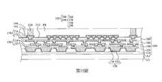
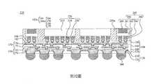
第1圖至第19圖為根據本揭露之一些實施方式之製造封裝結構的中間階段之剖面圖。1 to 19 are cross-sectional views of intermediate stages of manufacturing a package structure according to some embodiments of the present disclosure.
第20圖為根據本揭露之一些實施方式之半導體組件的剖面圖。FIG. 20 is a cross-sectional view of a semiconductor device according to some embodiments of the present disclosure.
第21圖至第22圖為在第17圖之步驟後的製造封裝結構的中間階段的剖面圖。Figures 21 to 22 are cross-sectional views of the intermediate stages of manufacturing the package structure after the step of Figure 17;
第23圖為根據本揭露之一些實施方式之封裝結構的剖面圖。FIG. 23 is a cross-sectional view of a package structure according to some embodiments of the present disclosure.
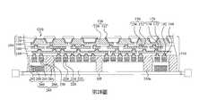
第24圖至第32圖為根據本揭露之一些實施方式之製造封裝結構的中間階段之剖面圖。Figures 24 to 32 are cross-sectional views of intermediate stages of manufacturing a package structure according to some embodiments of the present disclosure.
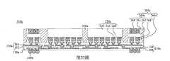
第33圖為根據本揭露之一些實施方式之模製封裝的剖面圖。Figure 33 is a cross-sectional view of a molded package according to some embodiments of the present disclosure.
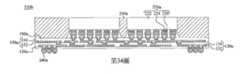
第34圖為根據本揭露之一些實施方式之模製封裝的剖面圖。Figure 34 is a cross-sectional view of a molded package according to some embodiments of the present disclosure.
第35圖為根據本揭露之一些實施方式之封裝結構的剖面圖。FIG. 35 is a cross-sectional view of a package structure according to some embodiments of the present disclosure.
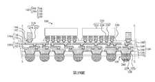
第36圖至第51圖為根據本揭露之一些實施方式之製造封裝結構的中間階段之剖面圖。FIGS. 36 to 51 are cross-sectional views of intermediate stages of manufacturing a package structure according to some embodiments of the present disclosure.
第52圖為根據本揭露之一些實施方式之積體扇出型封裝的剖面圖。FIG. 52 is a cross-sectional view of an integrated fan-out package according to some embodiments of the present disclosure.
第53圖為根據本揭露之一些實施方式之積體扇出型封裝的剖面圖。FIG. 53 is a cross-sectional view of an integrated fan-out package according to some embodiments of the present disclosure.
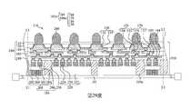
第54圖為根據本揭露之一些實施方式之封裝結構的剖面圖。FIG. 54 is a cross-sectional view of a package structure according to some embodiments of the present disclosure.
以下揭露提供許多不同實施方式或例子,以實現所提供之標的的不同特徵。下文描述之組件及排列之特定實例以簡化本揭露。當然,此等僅僅為實例且不意欲作為限制。例如,在隨後描述中在第二特徵上方或在第二特徵上之第一特徵之形成可包括第一及第二特徵形成為直接接觸之實施方式;以及亦可包括可在第一及第二特徵之間形成額外特徵,以使得第一及第二特徵可不直接接觸之實施方式。另外,本揭露可能在各實例中重複組件符號及/或字母。重複為出於簡易及清楚之目的,且本身不指示所論述之各種實施方式及/或配置之間關係。The following disclosure provides many different implementations or examples to achieve different features of the provided subject matter. Specific examples of components and arrangements are described below to simplify the disclosure. Of course, these are merely examples and are not intended as limitations. For example, in the following description, the formation of the first feature above or on the second feature may include an embodiment in which the first and second features are formed in direct contact; and may also include the first and second features. Extra featuresFeatures, so that the first and second features can not directly contact the implementation. In addition, the present disclosure may repeat component symbols and/or letters in each example. The repetition is for the sake of simplicity and clarity, and does not indicate the relationship between the various embodiments and/or configurations discussed.
另外,空間相對術語,諸如「在...之下」、「低於」、「下部」、「高於」、「上部」等,可在本文用以便於描述,以描述如在附圖中圖示之一個組件或特徵相對另一組件或特徵的關係。除圖形中描繪之方向外,空間相對術語意圖是包含在使用或操作中之裝置之不同的方向。裝置可為不同朝向(旋轉90度或以其他的方向)及可因此相應地解釋在本文中使用之空間相對的描述詞。In addition, spatially relative terms, such as "below", "below", "lower", "above", "upper", etc., can be used herein for the convenience of description, to describe as in the accompanying drawings The relationship of one component or feature relative to another component or feature shown in the figure. In addition to the directions depicted in the figures, the spatial relative terms are intended to include the different directions of the device in use or operation. The device can be in different orientations (rotated by 90 degrees or in other directions) and therefore the spatially relative descriptors used in this text can be interpreted accordingly.
本揭露亦可包含其他技術特徵及製程。例如,可包含測試結構以幫助三維封裝及三維積體電路裝置的驗證測試。測試結構可以包含,例如,在重分佈層中或基板上形成之測試墊,此測試墊允許三維封裝及三維積體電路之測試、使用探針及/或探針板、及類似物。上述驗證測試可以對中間結構以及最終結構執行。另外,本文揭露之結構及方法可以結合測試方法使用,此測試方法結合已知良好晶粒之中間驗證以增加良率與降低成本。This disclosure may also include other technical features and manufacturing processes. For example, a test structure may be included to assist verification testing of three-dimensional packaging and three-dimensional integrated circuit devices. The test structure may include, for example, test pads formed in the redistribution layer or on the substrate, which test pads allow three-dimensional packaging and three-dimensional integrated circuit testing, the use of probes and/or probe cards, and the like. The above verification test can be performed on the intermediate structure as well as the final structure. In addition, the structure and method disclosed in this article can be used in combination with a test method, which is combined with intermediate verification of known good dies to increase yield and reduce cost.
第1圖至第19圖為根據本揭露之一些實施方式之製造封裝結構的中間階段之剖面圖。參閱第1圖。黏膠層A1在載體C1上形成。載體C1可為空白玻璃載體、空白陶瓷載體、金屬框或類似物。黏膠層A1可由黏膠組成,諸如紫外光(ultra-violet;UV)膠、光熱轉換(light-to-heat conversion;LTHC)膠或類似物,雖然可以使用其他類型之黏膠。緩衝層110可例如用旋轉塗佈製程、薄膜層壓製程或沉積製程形成在黏膠層A1上方。緩衝層110為介電層,其可為聚合物層。聚合物層可以包括,例如聚醯亞胺、聚苯噁唑(PBO)、苯並環丁烯(BCB)、ajinomoto增設膜(ajinomoto buildup film;ABF)、阻焊(solder resist;SR)膜或類似物。在一些實施方式中,緩衝層110可為組合層,其結合緩衝層110與黏膠層A1於一個層中。緩衝層110可為大體上平坦的層,具有大體上均於的厚度,其中厚度可大於約2μm或可在0.5μm至約40μm之範圍中。在一些實施方式中,緩衝層110之頂面及底面亦為大體上平坦的。1 to 19 are cross-sectional views of intermediate stages of manufacturing a package structure according to some embodiments of the present disclosure. Refer to Figure 1. The adhesive layer A1 is formed on the carrier C1. The carrier C1 can be a blank glass carrier, a blank ceramic carrier, a metal frame or the like. The adhesive layer A1 can be composed of adhesive, such as ultraviolet (ultra-violet; UV) glue, light-to-heat conversion (light-to-heat)conversion; LTHC) glue or the like, although other types of glue can be used. The
參閱第2圖。例如,使用旋轉塗佈製程或層壓製程在緩衝層110上方形成介電層120。之後,介電層120經圖案化以形成開口O1。開口O1可以佈置在對應於隨後形成之球柵陣列(BGA)的行及列之柵格圖案中。介電層120可以使用微影製程圖案化。在一些實施方式中,介電層120可以為聚合物層。聚合物層可以包括,例如聚醯亞胺、聚苯噁唑(PBO)、苯並環丁烯(BCB)、ajinomoto增設膜(ABF)、阻焊(SR)膜或類似物。Refer to Figure 2. For example, a spin coating process or a lamination process is used to form the
參閱第3圖。晶種層132在載體C1上方形成。晶種層132在載體C1上之緩衝層110及介電層120上方形成。晶種層132包括例如鈦(Ti)、銅(Cu)或其組合,並且例如在一些實施方式中使用物理氣相沉積(physical vapor deposition;PVD)或藉由箔材料之層壓而沉積。或者,晶種層132可以包括其他材料及尺寸,且可使用其他方法形成。之後,光阻P1塗佈在晶種層132上方且隨後被圖案化。如此一來,開口O2在光阻P1中形成,且晶種層132之一些部分經由開口O2暴露。Refer to Figure 3. The
參閱第4圖。導體134經由鍍覆(其可為電鍍或無電電鍍)分別在光阻P1之開口O2中形成。導體134被電鍍在晶種層132之暴露部分上。導體134可以包括金屬或金屬合金,此金屬合金包括鋁、銅、鎢及/或其合金。在電鍍導體134之後,去除光阻P1以暴露晶種層132之一些部分。Refer to Figure 4. The
參閱第5圖。執行蝕刻操作以去除晶種層132之暴露部分,且蝕刻操作可以包括非等向性蝕刻。被導體134覆蓋之晶種層132的部分仍然未蝕刻。在本文中,導體134及其下方晶種層132的剩餘部分組合成為重分佈線(redistribution lines;RDL)130。雖然晶種層132繪示為與導體134分開之層,但是當晶種層132由類似於或大體上相同於其上導體134之材料組成時,晶種層132可以與導體134融合而在兩者間無可區分的界面。在替代實施方式中,在晶種層132與其上導體134之間存在可區分的界面。Refer to Figure 5. The etching operation is performed to remove the exposed portion of the
參閱第6圖。介電層140在重分佈線130上方形成。介電層140可以包括聚合物,諸如聚醯亞胺、苯並環丁烯(BCB)、聚苯噁唑(PBO)或類似物,其例如使用旋轉塗佈製程或層壓製程沉積。或者,介電層140可以包括非有機介電材料,諸如氧化矽、氮化矽、碳化矽、氮氧化矽或類似物。介電層140使用微影製程圖案化。例如,光阻(未繪示)可以在介電層140上方形成,以及光阻藉由暴露至能量或光而圖案化,此能量或光從其上具有預定圖案的微影遮罩反射或通過。顯影光阻,且使用灰化及/或蝕刻製程去除光阻之曝光(或未曝光,取決於光阻為正型還是負型)區域。光阻隨後在蝕刻製程期間作為蝕刻遮罩。介電層140之暴露部分在蝕刻製程期間去除以形成開口O3,經由開口O3暴露重分佈線130之一些部分。隨後去除光阻。Refer to Figure 6. The
參閱第7圖。晶種層152在載體C1上方形成。晶種層152在介電層140上方及在介電層140之開口O3(如第6圖所示)中形成。在一些實施方式中,晶種層152在介電層140及開口O3(如第6圖所示)上共形地形成。晶種層152包括例如鈦(Ti)、銅(Cu)或其組合,且例如在一些實施方式中使用物理氣相沉積(PVD)或藉由箔材料之層壓而沉積。或者,晶種層152可以包括其他材料且可使用其他方法形成。Refer to Figure 7. The
在形成晶種層152之後,光阻P2塗佈在晶種層152上方且隨後被圖案化。結果,開口O4在光阻P2中形成,晶種層152之一些部分經由開口O4暴露晶種層152。使用微影技術圖案化光阻P2以定義出在後續步驟中形成之導體154的圖案。導體154例如經由鍍覆(其可為電鍍或無電電鍍)分別在光阻P2之開口O4中形成。導體154被電鍍在晶種層152之暴露部分上。導體154可包括金屬或金屬合金,包括鋁、銅、鎢及/或其合金。After the
在電鍍導體154之後,去除光阻P2,及暴露晶種層152之一些部分。可執行蝕刻步驟以去除晶種層152之暴露部分,並且蝕刻步驟可以包括非等向性蝕刻。另一方面,被導體154覆蓋之晶種層152的部分仍然未蝕刻,結構如第8圖所示。導體154及晶種層152之剩餘部分可共同地成為重分佈線(RDL)150。雖然晶種層152繪示為與導體154分隔之層,但是當晶種層152由類似於或大體上相同於其上導體154之材料組成時,晶種層152可以與導體154融合而在兩者間無可區分的界面。在替代實施方式中,在晶種層152與其上導體154之間存在可區分的界面。After electroplating the
參閱第9圖。介電層160在重分佈線150上方形成,使得重分佈線150嵌入介電層160中。介電層160可以包括聚合物,諸如聚醯亞胺、苯並環丁烯(BCB)、聚苯噁唑(PBO)或類似物,及例如使用旋轉塗佈製程或層壓製程沉積。或者,介電層160可以包括非有機介電材料,諸如氧化矽、氮化矽、碳化矽、氮氧化矽或類似物。介電層160使用微影製程圖案化。例如,光阻(未繪示)可以在介電層160上方形成,以及光阻藉由暴露至能量或光而圖案化,此能量或光從其上具有預定圖案的微影遮罩反射或通過。顯影光阻,且使用灰化及/或蝕刻製程去除光阻之曝光(或未曝光,取決於光阻為正型還是負型)區域。光阻隨後在蝕刻製程期間作為蝕刻遮罩。介電層160之暴露部分在蝕刻製程期間經去除以形成開口O5,重分佈線150之一些部分經由開口O5暴露。Refer to Figure 9. The
重分佈線之層數及介電層之數目並不限制本揭露之各種實施方式。例如,在形成第9圖之結構之後,第10圖中所示的另一層重分佈線170及另一介電層180可經由第6圖至第9圖所示之步驟在重分佈線150及介電層160上方形成。為了簡化描述,形成重分佈線170及介電層180之步驟不再重複贅述。The number of layers of redistribution lines and the number of dielectric layers do not limit the various embodiments of the present disclosure. For example, after the structure in FIG. 9 is formed, another layer of
參閱第10圖。介電層180經圖案化而形成開口O6以暴露重分佈線170之一些部分。之後,毯覆晶種層192在介電層180及暴露之重分佈線170上方形成,如第11圖所示。Refer to Figure 10. The
參閱第12圖。光阻P3塗佈在晶種層192上方且隨後被圖案化。如此一來,開口O7在光阻P3中形成,晶種層192之一些部分由開口O7暴露。後來,導體194經由鍍覆方法分別在光阻P3之開口O7中形成,鍍覆方法可為電鍍或無電電鍍。導體194被電鍍在晶種層192之暴露部分上。在電鍍導體194之後,去除光阻P3以暴露晶種層192之一些部分。Refer to Figure 12. The photoresist P3 is coated on the
參閱第13圖。執行蝕刻操作以去除晶種層192之暴露部分,並且蝕刻操作可以包括非等向性蝕刻。另一方面,被導體194覆蓋之晶種層192的部分仍然未被蝕刻。Refer to Figure 13. An etching operation is performed to remove the exposed portion of the
緩衝層110、介電層120、重分佈線130、介電層140、重分佈線150、介電層160、重分佈線170、介電層180、晶種層192及導體194可共同地作為重分佈結構102。在一些實施方式中,緩衝層110、介電層120、140、160、180可作為重分佈結構102之介電結構104。重分佈線130、150、170、晶種層192及導體194可作為重分佈結構102之佈線結構106。The
參閱第14圖。晶種層212例如經由PVD或金屬箔層壓在重分佈結構102上形成。晶種層212可以包括銅、銅合金、鋁、鈦、鈦合金或其組合。在一些實施方式中,晶種層212包括鈦層及在鈦層上方之銅層。在替代實施方式中,晶種層212為銅層。之後,光阻P4塗佈在晶種層212上方且隨後經圖案化而暴露晶種層212之一些部分。如此一來,開口O8在光阻P4中形成,晶種層212之一些部分經由開口O8暴露。Refer to Figure 14. The
參閱第15圖。導體214經由例如鍍覆方法分別在光阻P4之開口O8中形成,鍍覆方法可為電鍍、無電電鍍或金屬膏印刷。導體214分別被電鍍在開口O8下之晶種層212的暴露部分上。導體214可以包括銅、鋁、鎢、鎳、焊料、銀或其合金。導體214之俯視形狀可為矩形、正方形、圓形或類似形狀。在電鍍導體214之後,去除光阻P4,且暴露晶種層212之一些部分。Refer to Figure 15. The
參閱第16圖。執行蝕刻步驟以去除未被導體214覆蓋之晶種層212的暴露部分,其中蝕刻步驟可包括非等向性蝕刻。另一方面,由導體214覆蓋之晶種層212的部分仍然未被蝕刻。在本文中,導體214及其下晶種層212之剩餘部分組合地作為積體扇出(through integrated fan-out;InFO)通孔(TIV)210,其亦稱為通孔。雖然晶種層212繪示為與導體214分隔之層,但是當晶種層212由類似於或大體上相同於其上導體214之材料組成時,晶種層212可以與導體214融合而在兩者之間沒有可區分的界面。在替代實施方式中,在晶種層212與其上導體214之間存在可區分的界面。Refer to Figure 16. An etching step is performed to remove the exposed portion of the
在形成積體扇出通孔210之後,暴露未被導體214覆蓋之一些導體194,以便後續放置之半導體裝置220(見第17圖)可經由預先暴露之導體194電連接至重分佈結構102。在放置半導體裝置220之前形成重分佈結構102的方法在本文可稱作「RDL為先」(RDL-first)製程。After the integrated fan-out via 210 is formed, some
參閱第17圖。使用拾取及放置的機器、人工等等將半導體裝置220設置在或放置在重分佈結構102上。半導體裝置220之數目並不限制本揭露之各種實施方式。半導體裝置220之厚度可為相同的或不同的,且本揭露之各種實施方式並不限於此。半導體裝置220可電連接至未被積體扇出通孔210覆蓋之重分佈結構102的一些導體194。例如,半導體裝置220之底部上之接合墊224(諸如銅墊)電連接至導體194。換言之,使用「覆晶」(flip chip)方法將半導體裝置220設置在重分佈結構102上;即,在半導體裝置220之面上的接合墊224經「翻轉」,所以它們「面朝下」,且接合墊224使用導電材料連接至導體194。例如,接合墊224可經由連接件226電連接及機械連接至重分佈結構102之暴露的導體194。在一些實施方式中,導體194形成為墊,連接件226可以為焊料凸塊或焊球,這些焊料凸塊或焊球實體接觸導體194而形成墊上焊料(solder-on-pad;SOP)連接物。在一些其他實施方式中,導體194可以形成為走線(trace),及連接件226可以包括非焊料金屬凸塊。非焊料金屬凸塊可以包括銅柱且可以包括一或多個包括鎳、金、鈀或其他適宜材料的層。這些非焊料金屬凸塊(例如,連接件226之代替類型)及導體194可以藉由焊料接合以形成走線上凸塊(bump-on-trace;BOT)連接物。藉由連接件226形成之SOP連接物或BOT連接物,半導體裝置220可以與重分佈結構102電連接。Refer to Figure 17. The
如第17圖所示,根據一些實施方式,在「RDL為先」製程形成的結構中,底部填充層230可選擇性地形成在半導體裝置220與重分佈結構102之間,及連接件226之間。底部填充層230可以使用毛細底部填充(capillary underfill;CUF)方法作為液體施配(dispense)。樹脂或環氧樹脂液體在半導體裝置220下方流動,且填充在半導體裝置220與重分佈結構102之間的空間。室溫、UV或熱固化可以用以固化底部填充層230。底部填充層230可至少對其上的半導體裝置220及其下的重分佈結構102提供機械強度及應力消除。在一些實施方式中,底部填充層230與後續用來模製半導體裝置220形成的模製化合物250(見第22圖)相同。即,在半導體裝置220與重分佈結構102之間的空間可以由後續形成之模製化合物250填充。As shown in FIG. 17, according to some embodiments, in the structure formed by the "RDL first" process, an
在一些實施方式中,半導體裝置220為未封裝半導體裝置,諸如邏輯裝置晶粒(例如,加速處理單元(accelerated processing unit;APU)、圖形處理單元(graphics processing unit;GPU)、壓電多層促動器(piezoelectric multilayer actuator;PMA)、壓電促動器(piezoelectric actuator;PA)等等),記憶體裝置晶粒(例如,低功率雙倍資料速率(low power double-data-rate;LPDDR)、快閃(flash)、高頻寬記憶體(high bandwidth memory;HBM)等等),或感測裝置晶粒(例如,接觸影像感測器(contact image sensor;CIS)、微電機系統(micro-electro-mechanical system;MEMS)等等)。在一些實施方式中,半導體裝置220設計來用於行動應用且可為中央計算單元(central computing unit;CPU)晶粒、功率管理積體電路(power management integrated circuit;PMIC)晶粒、收發器(transceiver;TRX)晶粒或類似物。半導體裝置220包括半導體基板222(例如矽基板),以及自半導體裝置220之底部介電層(未繪示)凸出或齊平的接合墊224。In some embodiments, the
參閱第18圖。重分佈結構102從載體C1脫離。黏膠層A1亦自重分佈結構102之緩衝層110清除。去除黏膠層A1之結果會暴露重分佈結構102之緩衝層110。在一些實施方式中,第18圖所示之結構黏附至切割膠帶(未繪示)。在一些實施方式中,層壓薄膜(未繪示)可放置在暴露之緩衝層110上,其中層壓薄膜可以包括SR、ABF、背面塗層膠帶或類似物。在替代實施方式中,沒有層壓膜放置在緩衝層110上方。Refer to Figure 18. The
參閱第19圖。圖案化緩衝層110以形成開口O9,藉此暴露重分佈線130。在一些實施方式中,執行雷射鑽孔製程以形成開口O9以去除緩衝層110之部分及晶種層132之部分。即,開口O9可為雷射鑽孔開口。雷射鑽孔製程可以產生開口O9之側壁的鋸齒輪廓或粗糙輪廓。在一些其他實施方式中,光微影製程亦可用以形成開口O9以去除緩衝層110之部分,隨後執行蝕刻步驟以去除晶種層132之暴露部分,其中蝕刻步驟可包括非等向性蝕刻。如此一來,導體134之部分經由開口O9而暴露。在一些實施方式中,開口O9佈置在行及列之柵格圖案中,以便後續在開口O9中形成之導電凸塊(例如,導電球體240)能形成BGA。Refer to Figure 19. The
導電球體240在重分佈線130之暴露部分上形成。換言之,導電球體240電連接至重分佈線130。如此一來,導電球體240可經由重分佈線130電偶接至重分佈線150。導電球體240之形成可以包括在緩衝層110之開口O9中放置焊球,且隨後將焊球回焊。因此,導電球體240部分嵌入式地保留在緩衝層110之開口O9中。在形成導電球體240之後,執行切割製程沿線L-L切割介電結構104,使得至少一個半導體組件100能形成。在一些實施方式中,此組件黏附至切割膠帶,此切割膠帶可在切割製程之後去除。The
在形成導電球體240之後,可對重分佈結構102、半導體裝置220及積體扇出通孔210執行電性測試,其可有助於在模製半導體裝置220及積體扇出通孔210之前解決一些問題(例如,缺陷/可靠度)。換言之,根據本揭露之一些實施方式之RDL為先的製程允許經由如導電球體240對中間封裝執行電性測試。以這種方法,中間封裝,即半導體組件100,當其通過電性測試時可確定為已知良好的封裝。另外,半導體組件100對熱敏感的半導體裝置220是有益的,因為重分佈結構102是在設置半導體裝置220之前形成,而重分佈結構102是被施以高溫製程的,因此能避免半導體裝置220損壞。After the
第20圖為根據本揭露之一些實施方式之半導體組件100a的剖面圖。半導體組件100a可以藉由如上所述之半導體組件100的製造步驟而形成。半導體組件100a具有重分佈線130a及比半導體組件100之導電球體240數量少的導電球體240a。重分佈線130a位於介電層120a中且電連接至半導體裝置220a及積體扇出通孔210a,且導電球體240a電連接至重分佈線130a。在一些實施方式中,半導體組件100a包括半導體裝置220a,其與第19圖之半導體裝置220相同。在替代實施方式中,第20圖之半導體裝置220a不同於第19圖之半導體裝置220,本揭露之各種實施方式並不限於此。FIG. 20 is a cross-sectional view of a
在形成第19圖之半導體組件100及第20圖之至少一個半導體組件100a之後,半導體組件100a經由半導體組件100a之導電球體240a及半導體組件100之積體扇出通孔210接合至半導體組件100。導電球體240a分別與積體扇出通孔210大體上對齊。如此一來,半導體組件100a可堆疊在半導體組件100上。After the
在一些實施方式中,半導體組件100a之積體扇出通孔210a分別與導電球體240a大體上對齊。這樣的配置,至少兩個半導體組件100a可經由上半導體組件100a之導電球體240a及下半導體組件100a之積體扇出通孔210a堆疊。In some embodiments, the integrated fan-out through
第21圖至第22圖為在第19圖之步驟後的製造封裝結構的中間階段的剖面圖。參閱第21圖。在形成半導體組件100及多個半導體組件100a之後,半導體組件100a其中之一經由半導體組件100a底側之導電球體240a及半導體組件100頂側之積體扇出通孔210堆疊在半導體組件100上。如此一來,半導體組件100a之重分佈線130a接合至半導體組件100之重分佈線170。換言之,包括積體扇出通孔210及其上導電球體240a之導電件215電連接半導體組件100a之重分佈線130a與半導體組件100之重分佈線170。此外,包括積體扇出通孔210a及其上導電球體240a之導電件215a經由重分佈線150a電連接重分佈線130a。之後,其他半導體組件100a經由導電球體240a及積體扇出通孔210a依序堆疊在第一個堆疊的半導體組件100a上。在一些實施方式中,半導體組件100a為相同的。在其他實施方式中,半導體組件100a為不同的。例如,半導體組件100a可以具有不同種類的半導體裝置220a、不同層數的重分佈線150a、及/或不同佈局的重分佈線150a。21 to 22 are cross-sectional views of the intermediate stage of manufacturing the package structure after the steps in FIG. 19. Refer to Figure 21. After the
在半導體組件100a接合至半導體組件100後,半導體封裝300接合至上半導體組件100a。半導體封裝300在半導體組件100a及半導體組件100之堆疊組件上方。在一些實施方式中,半導體封裝300包括基板320,及導電凸塊或導電球體330。導電凸塊330自基板320凸出。此外,半導體封裝300之導電凸塊330分別與上半導體組件100a之積體扇出通孔210a大體上對齊。在這種配置中,半導體封裝300可經由半導體封裝300底側之導電凸塊330及上半導體組件100a頂側之積體扇出通孔210a接合至上半導體組件100a,使得半導體封裝300經由導電凸塊330電連接至其下的積體扇出通孔210a。然而,前述步驟之順序並不用以限制本揭露之各種實施方式。例如,接合半導體組件100a以形成堆疊結構,隨後半導體封裝300接合至堆疊結構之頂側。之後,堆疊結構之下側接合至半導體組件100,使得第21圖之結構仍可獲得。在一些實施方式中,半導體封裝300可以為記憶體裝置,諸如靜態隨機存取記憶體(static random access memory;SRAM)或動態隨機存取記憶體(dynamic random access memory;DRAM)裝置。半導體封裝300可以包括在其內的複數個堆疊記憶體晶粒。此外,半導體封裝300之其他類型也可位於半導體組件100a上,本揭露之各種實施方式並不限於此。After the
參閱第22圖。在形成如第21圖圖示之堆疊結構後,模製材料(或模製化合物)250模製半導體裝置220、半導體裝置220a、積體扇出通孔210、積體扇出通孔210a及導電球體240a、導電球體330。半導體封裝300在模製材料250上方。換言之,模製材料250在半導體組件100與其上半導體組件100a之間、兩個相鄰半導體組件100a之間、及半導體封裝300與其下半導體組件100a之間形成。此外,模製材料250圍繞半導體裝置220、半導體裝置220a、積體扇出通孔210、積體扇出通孔210a及導電球體240a、導電球體330。模製材料250填充半導體裝置220與積體扇出通孔210之間的縫隙及填充半導體裝置220a與積體扇出通孔210a之間的縫隙。另外,模製材料250具有在半導體裝置220與介電層120a(或緩衝層110a)之間的部分。積體扇出通孔210、導電球體240a、及積體扇出通孔210a與模製材料250接觸。模製材料250可與介電層180、介電層160a、緩衝層110a及基板320接觸。在形成模製材料250之後,半導體組件100及其上模製材料250形成積體扇出型封裝410,且半導體組件100a及其上模製材料250形成積體扇出型封裝410a。因此,積體扇出型封裝410、積體扇出型封裝410a及半導體封裝300之組合形成封裝結構400,所得之結構如第22圖所示。Refer to Figure 22. After forming the stacked structure as shown in FIG. 21, the molding material (or molding compound) 250 molds the
在一些實施方式中,模製材料250包括聚合物基材料。「聚合物」可表示熱固性聚合物、熱塑性聚合物、或其任何混合物。聚合物基材料可包括例如塑性材料、環氧樹脂、聚醯亞胺、聚對苯二甲酸乙二酯(PET)、聚氯乙烯(PVC)、聚甲基丙烯酸甲酯(PMMA)、摻雜有填充劑(包括纖維、黏土、陶瓷、無機顆粒)之聚合物化合物、或其任意組合。In some embodiments, the
因為單一模製步驟可讓模製材料250能填充在半導體組件100與其上半導體組件100a之間、兩個相鄰半導體組件100a之間、及在半導體封裝300與其下半導體組件100a之間的縫隙,所以可以減少製造封裝結構400之週期時間(cycle time)及翹曲。Because a single molding step allows the
此外,當封裝結構400設置在印刷電路板(printed circuit board;PCB)上時,封裝結構400佔據與半導體組件100、半導體組件100a或半導體封裝300之面積相同的印刷電路板面積,因此印刷電路板被半導體組件100、半導體組件100a及半導體封裝300佔據的面積得以縮小。In addition, when the
由於封裝結構400為三維層疊封裝(PoP)結構,因此積體扇出型封裝410、積體扇出型封裝410a及半導體封裝300之間之短長度及高頻寬通訊可提升設有封裝結構400之系統的效能。此外,封裝結構400可以包括各種半導體裝置(例如,220及220a)及半導體封裝310,以便由設計者彈性使用。Since the
在一些實施方式中,積體扇出型封裝410其內具有更多的半導體裝置220,積體扇出型封裝410a之至少一個其內具有更多的半導體裝置220a。這樣的配置結果,積體扇出型封裝410a之層數可以減少,但封裝結構400仍可具有相同的功能。此外,可降低封裝結構400之總高度。In some embodiments, the integrated fan-out
第23圖為根據本揭露之一些實施方式之封裝結構400a的剖面圖。封裝結構400a包括積體扇出型封裝410、積體扇出型封裝410a及在其上的積體扇出型封裝410b。積體扇出型封裝410b及積體扇出型封裝410a之間的差異為在積體扇出型封裝410b中沒有積體扇出通孔210a及其下導體194a。積體扇出型封裝410b之導電球體240b與其下積體扇出型封裝410a之積體扇出通孔210a大體上對齊,因此積體扇出型封裝410b之導電球體240b可分別接合至其下積體扇出型封裝410a之積體扇出通孔210a。FIG. 23 is a cross-sectional view of a
第24圖至第32圖為根據本揭露之一些實施方式之製造封裝結構的中間階段之剖面圖。參閱第24圖。包括介電結構104及佈線結構106a之重分佈結構102a在載體C1上形成。重分佈結構102a之形成類似上述之第1圖至第13圖所描述之重分佈結構102的形成,不再重複贅述。第24圖之佈線結構106a的圖案不同於第13圖之佈線結構106的圖案,但本揭露之各種實施方式並不限於此。Figures 24 to 32 are cross-sectional views of intermediate stages of manufacturing a package structure according to some embodiments of the present disclosure. Refer to Figure 24. The
參閱第25圖。導電件265包括被動嵌入件260及導電凸塊266。在一些實施方式中,被動嵌入件260為矽通孔(through silicon via;TSV)裝置。半導體裝置220及矽通孔裝置260使用拾取及放置機器、人工或其他適宜方法設置在或放置在重分佈結構102a上。矽通孔裝置260在介電層180上方,且矽通孔268在矽通孔裝置260中且電連接至接觸墊264。導電凸塊266在矽通孔裝置260與重分佈線170之間且電連接矽通孔裝置260與重分佈線170。半導體裝置220之數目及矽通孔裝置260之數目不限制本揭露之各種實施方式。半導體裝置220及矽通孔裝置260可電連接至重分佈結構102a之導體194。半導體裝置220之接合墊224及矽通孔裝置260之接觸墊264使用導電材料連接至導體194。例如,接合墊224可經由連接件226電連接及機械連接至一些導體194,連接件226例如導電凸塊,且接觸墊264可經由導電凸塊266電連接及機械連接至其餘導體194。Refer to Figure 25. The
如在第25圖之組件所示,根據一些實施方式,在由「RDL為先」製程形成的結構中,底部填充層230可選擇性地在半導體裝置220與重分佈結構102a之間及連接件226之間形成,且可選擇性地在矽通孔裝置260與重分佈結構102a之間及導電球體266之間形成。As shown in the component in FIG. 25, according to some embodiments, in the structure formed by the "RDL first" process, the
在一些實施方式中,矽通孔裝置260可包括例如,矽通孔(TSV)268及整合式被動元件(IPD,未繪示)。矽通孔裝置260允許高密度之結構於在其內形成,諸如矽通孔268及/或整合式被動元件。在一些實施方式中,矽通孔裝置260包含基板261,基板261包含半導體材料,諸如矽或類似物。基板261中之孔可充滿導體以形成矽通孔268及整合式被動元件,諸如溝槽電容器。矽通孔裝置260包含互連層262,其包括一或多層其內形成導電件的介電材料。在一些實施方式中,互連層262中之介電材料層由感光材料形成,諸如聚苯噁唑(PBO)、聚醯亞胺(PI)、苯並環丁烯(BCB)或類似物。在替代實施方式中,互連層262中之介電材料層可由諸如氮化矽的氮化物、諸如氮化矽的氧化物形成、磷矽酸鹽玻璃(PSG)、矽酸硼玻璃(BSG)、硼摻雜磷矽酸鹽玻璃(BPSG)或類似物形成。在一些替代實施方式中,互連層262可以包含嵌入件或封裝基板,諸如矽嵌入件、有機基板、層壓基板(例如,1-2-1層壓基板)或類似物。互連層262在相對側之間提供電連接且可作為佈線結構。外部接觸墊264組例如使用導電凸塊266提供外部電連接。In some embodiments, the through silicon via
如圖所示,相鄰矽通孔268的間距(pitch)比鄰近積體扇出通孔(例如,如前所述之積體扇出通孔210或積體扇出通孔210a)之間距短,因此若矽通孔268與凸塊接合,則具有較短間距之矽通孔268允許高密度凸塊。As shown in the figure, the pitch of
參閱第26圖。模製材料(或模製化合物)250a模製在重分佈結構102a、半導體裝置220及矽通孔裝置260上。模製材料250a填充在半導體裝置220與矽通孔裝置260之間的縫隙中,且可與重分佈結構102a接觸,例如接觸重分佈結構102a之介電層180。模製材料250a之頂面高於半導體裝置220及矽通孔裝置260之頂面。Refer to Figure 26. The molding material (or molding compound) 250a is molded on the
在一些實施方式中,模製材料250a包括聚合物基材料。「聚合物」可表示熱固性聚合物、熱塑性聚合物、或其任何混合物。聚合物基材料可包括例如塑性材料、環氧樹脂、聚醯亞胺、聚對苯二甲酸乙二酯(PET)、聚氯乙烯(PVC)、聚甲基丙烯酸甲酯(PMMA)、摻雜有填充劑(包括纖維、黏土、陶瓷、無機顆粒)之聚合物化合物、或其任意組合。In some embodiments, the
參閱第27圖。接下來,執行諸如研磨之平坦化製程以使模製材料250a變薄,直到暴露半導體裝置220及矽通孔裝置260之頂面。模製材料250a圍繞半導體裝置220及矽通孔裝置260。在一些實施方式中,在研磨模製材料250a後亦暴露在矽通孔裝置260頂面的矽通孔268。所得之結構如第27圖所示,其中模製材料250a與半導體裝置220及矽通孔裝置260之側壁接觸。由於研磨,半導體裝置220之頂面與矽通孔裝置260之頂面大體上齊平(共面),且與模製材料250a之頂面大體上齊平(共面)。研磨之結果,可能會產生諸如金屬顆粒之導電殘留物,並留在第27圖之結構的頂面上。因此,在研磨之後,清洗製程(例如經由濕式蝕刻)可以執行以去除導電殘留物。Refer to Figure 27. Next, a planarization process such as grinding is performed to thin the
參閱第28圖。接下來,模製封裝510從載體C1脫離。黏膠層A1亦自模製封裝510清除。去除黏膠層A1之結果,可暴露緩衝層110。參閱第28圖,具有半導體裝置220、模製材料250a及在其上之矽通孔裝置260的模製封裝510進一步黏附至切割膠帶DT,其中模製材料250a朝向切割膠帶DT且可接觸切割膠帶DT。在一些實施方式中,層壓薄膜(未繪示)置於暴露之緩衝層110上,其中層壓薄膜可包括ajinomoto增設膜(ABF)、阻焊(SR)膜、背面塗層膠帶或類似物。在替代實施方式中,沒有層壓薄膜置於緩衝層110上方。Refer to Figure 28. Next, the molded
開口O10在緩衝層110中形成。在形成緩衝層110之開口O10之後,經由開口O10暴露重分佈線130之晶種層132的部分。在一些實施方式中,執行雷射鑽孔製程以形成開口O10。在一些其他實施方式中,光微影製程亦可用以形成開口O10。之後,執行蝕刻步驟以去除晶種層132之暴露部分,其中蝕刻步驟可以包括非等向性蝕刻。如此一來,在晶種層132下之導體134的部分由開口O10暴露,以便接受後續形成的導電球體240(見第29圖)。在一些實施方式中,開口O10佈置在行及列之柵格圖案中,使後續在開口O10中形成之導電球體240可形成球柵陣列(BGA)。The opening O10 is formed in the
參閱第29圖。諸如導電球體240之導電凸塊在導體134之暴露部分上形成。換言之,導電球體240分別與導體134接觸,使得導電球體240可電連接至導體134。如此一來,導電球體240可經由導體134電偶接至佈線結構106a。導電球體240之形成可以包括在開口O10中放置焊球,且隨後將焊球回焊。Refer to Figure 29. Conductive bumps such as the
在形成導電球體240之後,執行切割製程以沿線L1切割介電結構104及模製材料250a,且也可去除切割膠帶DT,以形成複數個晶片尺寸模製封裝510。After the
在替代實施方式中,在脫離載體C1及清除黏膠層A1之後,執行一或多個蝕刻操作以去除緩衝層110及晶種層132之水平部分直到暴露導體134。所得之結構如第30圖所示,其中重分佈線130之頂面被暴露且與剩餘介電層120之頂面大體上齊平。在蝕刻製程之後,導電球體240在暴露之重分佈線130上形成,所得之結構如第31圖所示。In an alternative embodiment, after separating the carrier C1 and removing the adhesive layer A1, one or more etching operations are performed to remove the horizontal portions of the
在形成導電球體240之後,執行切割製程以沿線L1切割介電結構104及模製材料250a,且也可去除切割膠帶DT,以形成複數個晶片尺寸模製封裝510,所得之結構如第32圖所示。在以下敘述中,第31圖之重分佈線130、導電球體240及介電層120形成於第32圖至第35圖之封裝中。在一些替換性實施方式中,第29圖之重分佈線130、導電球體240、緩衝層110及介電層120可形成在第32圖至第35圖之封裝中,本揭露之各種實施方式不限於此。After the
第33圖為根據本揭露之一些實施方式之模製封裝510a的剖面圖。模製封裝510a可以藉由模製封裝510之前述製造步驟而形成。與模製封裝510相較,模製封裝510a具有在其內之重分佈線130a,且具有分別與模製封裝510其上矽通孔裝置260大體上對齊的導電球體240a。在一些實施方式中,模製封裝510a包括分別與第32圖之半導體裝置220及矽通孔裝置260相同的半導體裝置220a及矽通孔裝置260a。在替代實施方式中,半導體裝置220a及矽通孔裝置260a分別不同於第32圖之半導體裝置220及矽通孔裝置260,本揭露之各種實施方式不限於此。Figure 33 is a cross-sectional view of a molded
第34圖為根據本揭露之一些實施方式之模製封裝510b的剖面圖。在一些實施方式中,第29圖之矽通孔裝置260a為可選擇的。模製封裝510b在模製材料250a中沒有矽通孔裝置,但在介電層160a上具有更多的模製材料250a以補充空缺。Figure 34 is a cross-sectional view of a molded
第35圖為根據本揭露之一些實施方式之封裝結構500的剖面圖。在形成第32圖之模製封裝510,第33圖之至少一個模製封裝510a及第34圖之模製封裝510b後,模製封裝510b經由其導電球體240a及下方模製封裝510a之矽通孔裝置260a接合至模製封裝510a,且模製封裝510a經由其導電球體240a及模製封裝510之矽通孔裝置260接合至模製封裝510。導電球體240a在模製封裝510之矽通孔裝置260與模製封裝510a之重分佈線130a之間,且電連接模製封裝510之矽通孔裝置260與模製封裝510a之重分佈線130a。因此,模製封裝510b之導電球體240a電連接至模製封裝510a之矽通孔裝置260a之矽通孔268,且模製封裝510a之導電球體240a電連接至模製封裝510之矽通孔裝置260的矽通孔268。換言之,包括矽通孔裝置260、導電球體266及導電球體240a之導電件265電連接模製封裝510a之重分佈線130a與模製封裝510之重分佈線170。此外,包括矽通孔裝置260a、導電球體266a及導電球體240a之導電件265a經由重分佈線150a電連接至重分佈線130a。這樣的配置,模製封裝510b在模製封裝510a上堆疊,且模製封裝510a在模製封裝510上堆疊,進而形成封裝結構500。FIG. 35 is a cross-sectional view of a
在一些實施方式中,模製封裝510a之矽通孔裝置260a與模製封裝510a之導電球體240a大體上對齊,因此至少兩個模製封裝510a可經由上模製封裝510a之導電球體240a及下模製封裝510a之矽通孔裝置260a而堆疊。例如,封裝結構500包括三個模製封裝510a,但本揭露之各種實施方式不限於此。In some embodiments, the through-silicon via
在一些實施方式中,底部填充UF選擇性地設置在模製封裝510b與其下模製封裝510a之間,在兩個相鄰模製封裝510a之間、及在模製封裝510a與其下模製封裝510之間,使得模製封裝510b穩固地置於模製封裝510a上,且模製封裝510a穩固地置於另一模製封裝510a或模製封裝510上。In some embodiments, the underfill UF is selectively disposed between the molded
第36圖至第51圖為根據本揭露之一些實施方式之製造封裝結構的中間階段之剖面圖。參閱第36圖。黏膠層A3在載體C3上形成。載體C3可為空白玻璃載體、空白陶瓷載體或類似物。黏膠層A3可由黏膠組成,諸如紫外線(UV)膠、光熱轉換(LTHC)膠或類似物,雖也可使用其他類型之黏膠。緩衝層610在黏膠層A3上方形成。緩衝層610為介電層,其可為聚合物層。聚合物層可以包括,例如聚醯亞胺、聚苯噁唑(PBO)、苯並環丁烯(BCB)、ajinomoto增設膜(ABF)、阻焊(SR)膜或類似物。FIGS. 36 to 51 are cross-sectional views of intermediate stages of manufacturing a package structure according to some embodiments of the present disclosure. Refer to Figure 36. The adhesive layer A3 is formed on the carrier C3. The carrier C3 may be a blank glass carrier, a blank ceramic carrier or the like. The adhesive layer A3 can be composed of glue, such as ultraviolet (UV) glue, light-to-heat conversion (LTHC) glue or the like, although other types of glue can also be used. The
參閱第37圖。晶種層623例如經由物理氣相沉積(PVD)或金屬箔層壓而在緩衝層610上形成。晶種層623可以包括銅、銅合金、鋁、鈦、鈦合金或其組合。在一些實施方式中,晶種層623包括鈦層及在鈦層上方之銅層。在替代實施方式中,晶種層623為銅層。Refer to Figure 37. The
參閱第38圖。光阻P11塗佈在晶種層623上方且隨後被圖案化。如此一來,開口O11在光阻P11中形成,經由開口O11暴露晶種層623之一些部分。Refer to Figure 38. The photoresist P11 is coated on the
參閱第39圖。導體625經由鍍覆(其可為電鍍或無電電鍍)在光阻P11中形成。導體625被電鍍在晶種層623之暴露部分上。導體625可以包括銅、鋁、鎢、鎳、焊料或其合金。導體625之高度由後續放置之半導體裝置630(見第42圖)決定,其中在本揭露之一些實施方式中導體625之高度大於半導體裝置630之厚度。在鍍覆導體625後,去除光阻P11,且所得之結構如第40圖所示。在去除光阻P11後,暴露晶種層623之一些部分。Refer to Figure 39. The
參閱第41圖。可執行蝕刻步驟以去除晶種層623之暴露部分,其中蝕刻步驟可以包括非等向性蝕刻。另一方面,由導體625覆蓋之晶種層623的一些部分仍未被蝕刻。在本文中,導體625及其下晶種層623之剩餘部分組合地作為導電件620,為積體扇出(InFO)通孔(TIV),其亦稱為通孔。雖然晶種層623繪示為與導體625分隔之層,但是當晶種層623由類似於或大體上相同於其上導體625之材料組成時,晶種層623可以與導體625融合而在兩者之間沒有可區分的界面。在替代實施方式中,在晶種層623與其上導體625之間存在可區分的界面。Refer to Figure 41. An etching step may be performed to remove the exposed portion of the
第42圖繪示在緩衝層610上方放置半導體裝置630。半導體裝置630可經由黏膠層631黏附至緩衝層610。在一些實施方式中,半導體裝置630為非封裝的半導體裝置,即裝置晶粒。例如,半導體裝置630可為其內包括邏輯電晶體之邏輯裝置晶粒。在一些實施方式中,半導體裝置630經設計以用於行動應用,且可以為中央計算單元(CPU)晶粒、功率管理積體電路(PMIC)晶粒、收發器(TRX)晶粒或類似物。每個半導體裝置630包括接觸黏膠層631之半導體基板632(例如,矽基板),其中半導體基板632之背表面接觸黏膠層631。FIG. 42 shows that the
在一些實施方式中,導電柱636(諸如銅柱)形成為半導體裝置630之頂部,且電偶接至諸如半導體裝置630中之電晶體(未繪示)的裝置。在一些實施方式中,介電層634在對應的半導體裝置630之頂面上形成,其中導電柱636具有至少在介電層634中的下部分。在一些實施方式中導電柱636之頂面與介電層634之頂面大體上齊平。或者,未形成介電層,且導電柱636自對應的半導體裝置630之頂部介電層凸出(未繪示)。In some embodiments, a conductive pillar 636 (such as a copper pillar) is formed on top of the
參閱第43圖。模製材料635在半導體裝置630及積體扇出通孔620上形成。模製材料635填充在半導體裝置630與積體扇出通孔620之間的縫隙,且可以接觸緩衝層610。此外,當導電柱636凸出金屬柱(未繪示此配置)時,模製材料635填充進導電柱636之間的縫隙中。模製材料635之頂面高於導電柱636及積體扇出通孔620之頂端。Refer to Figure 43. The
在一些實施方式中,模製材料635包括聚合物基材料。「聚合物」可表示熱固性聚合物、熱塑性聚合物、或其任意混合物。聚合物基材料可包括例如塑性材料、環氧樹脂、聚醯亞胺、聚對苯二甲酸乙二酯(PET)、聚氯乙烯(PVC)、聚甲基丙烯酸甲酯(PMMA)、摻雜有填充劑(包括纖維、黏土、陶瓷、無機顆粒)之聚合物化合物、或其任意組合。In some embodiments, the
接下來,執行研磨步驟以使模製材料635變薄,直到暴露導電柱636及積體扇出通孔620。所得之結構如第44圖所示,其中模製材料635接觸半導體裝置630及積體扇出通孔620之側壁。模製材料635圍繞半導體裝置630及積體扇出通孔620。由於研磨,積體扇出通孔620之頂端與導電柱636之頂端大體上齊平(共面),且與模製材料635之頂面大體上齊平(共面)。經由研磨的結果,可能生成諸如金屬顆粒之導電殘留物,且留在第44圖之結構的頂面上。因此,在研磨之後,清洗製程(例如經由濕式蝕刻)可以執行以去除導電殘留物。Next, a grinding step is performed to thin the
參閱第45圖。介電層640在積體扇出通孔620、模製材料635及半導體裝置630上方形成。介電層640可以包括聚合物,諸如聚醯亞胺、苯並環丁烯(BCB)、聚苯噁唑(PBO)或類似物,其例如使用旋轉塗佈製程或層壓製程沉積。或者,介電層640可以包括非有機介電材料,諸如氧化矽、氮化矽、碳化矽、氮氧化矽或類似物。介電層640使用微影製程圖案化。例如,光阻(未繪示)可以在介電層640上方形成,以及光阻藉由暴露至能量或光而圖案化,此能量或光從其上具有預定圖案的微影遮罩反射或通過。顯影光阻,且使用灰化及/或蝕刻製程去除光阻之曝光(或未曝光,取決於光阻為正型還是負型)區域。光阻隨後在蝕刻製程期間作為蝕刻遮罩。介電層640之暴露部分在蝕刻製程期間去除以形成開口O12,經由開口O12暴露積體扇出通孔620及導電柱636。接著,去除光阻。Refer to Figure 45. The
參閱第46圖。晶種層652在介電層640上方及介電層640之開口O12中形成。在一些實施方式中,晶種層652在介電層640上及開口O12中共形地形成。晶種層652包括諸如鈦(Ti)、銅(Cu)或其組合之約0.3μm之材料,其例如在一些實施方式中使用物理氣相沉積(PVD)或藉由箔材料之層壓而沉積。或者,晶種層652可以包括其他材料及尺寸且可使用其他方法形成。Refer to Figure 46. The
在形成晶種層652之後,光阻P12塗佈在晶種層652上方且隨後被圖案化。因此,開口O13在光阻P12中形成,經由開口O13暴露晶種層652之一些部分。使用微影圖案化光阻P12以進一步定義後續步驟中形成之導體654的圖案。導體654例如經由鍍覆(其可為電鍍或無電電鍍)分別在光阻P12之開口O13中形成。導體654被鍍覆在晶種層652之暴露部分上。導體654可包括金屬或金屬合金,此金屬合金包括鋁、銅、鎢及/或其合金。After the
在鍍覆導體654之後,去除光阻P12,且暴露晶種層652之一些部分。可執行蝕刻步驟以去除晶種層652之暴露部分,且蝕刻步驟可以包括非等向性蝕刻。另一方面,由導體654覆蓋之晶種層652的一些部分仍未被蝕刻,所得之結構如第47圖所示。導體654及晶種層652之剩餘部分可共同地作為重分佈線(RDL)650。雖然晶種層652繪示為與導體654分隔之層,但是當晶種層652由類似於或大體上相同於其上導體654之材料組成時,晶種層652可以與導體654融合而在兩者之間大體上沒有可區分的界面。在替代實施方式中,在晶種層652與其上導體654之間存在可區分的界面。After plating the
參閱第48圖。介電層640a在重分佈線650及介電層640上方形成,使得重分佈線650嵌入介電層640a中。介電層640a可以包括聚合物,諸如聚醯亞胺、苯並環丁烯(BCB)、聚苯噁唑(PBO)或類似物,其例如使用旋轉塗佈製程或層壓製程沉積。或者,介電層640a可以包括非有機介電材料,諸如氧化矽、氮化矽、碳化矽、氮氧化矽或類似物。介電層640a使用微影製程圖案化。例如,光阻(未繪示)可以在介電層640a上方形成,且光阻藉由暴露至能量或光而圖案化,此能量或光從其上具有預定圖案的微影遮罩反射或通過。顯影光阻,且使用灰化及/或蝕刻製程去除光阻之曝光(或未曝光,取決於光阻為正型還是負型)區域。光阻隨後在蝕刻製程期間作為蝕刻遮罩。介電層640a之暴露部分在蝕刻製程期間去除以形成開口O14,經由開口O14暴露重分佈線650之一些部分。See figure 48. The
重分佈線650之層數及介電層之數目並不限制本揭露之各種實施方式。例如,在形成第48圖之結構後,如第49圖繪示之重分佈線650a、重分佈線650b之層及介電層640b、介電層640c可經由第45圖至第48圖之前述步驟在重分佈線650及介電層640a上方形成。為了簡化描述,將不重覆贅述形成重分佈線650a、重分佈線650b及介電層640b、介電層640c之步驟。此外,第49圖之接觸墊660之形成類似於第3圖至第5圖之步驟。The number of layers of the
參閱第49圖。在介電層640c經圖案化以形成開口之後,晶種層662在介電層640c及開口中之重分佈線650b之暴露部分上方形成,隨後光阻塗佈在晶種層662上方且經圖案化以形成開口。接下來,導體664經由鍍覆分別在光阻之開口中形成,使得導體664被鍍覆在晶種層662之暴露部分上。在電鍍導體664後,去除光阻以暴露晶種層662之一些部分,隨後執行蝕刻操作以去除晶種層662之暴露部分。如此一來,導體664及其下晶種層662之剩餘部分組合地作為第49圖之接觸墊660。Refer to Figure 49. After the
雖然晶種層662繪示為與導體664分隔之層,但當晶種層662由類似於或大體上相同於其上導體664之材料組成時,晶種層662可以與導體664融合而在兩者之間大體上沒有可區分的界面。在替代實施方式中,在晶種層662與其上導體664之間存在可區分的界面。Although the
參閱第50圖。諸如導電球體670之導電凸塊在接觸墊660上形成。換言之,導電球體670分別與接觸墊660接觸,使導電球體670可電連接至接觸墊660。如此一來,導電球體670經由接觸墊660可電偶接至重分佈線650、重分佈線650a、重分佈線650b。在形成導電球體670之後,載體C3及黏膠層A3自緩衝層610去除。See figure 50. Conductive bumps such as
參閱第51圖。載體C3脫離及黏膠層A3去除之果,在半導體裝置630及模製材料635上方之緩衝層610被暴露。隨後緩衝層610經圖案化以形成開口O15,藉此暴露積體扇出通孔620。在一些實施方式中,執行雷射鑽孔製程以形成開口O15。在一些其他實施方式中,光微影製程亦可用以形成開口O15及去除緩衝層610之部分。在一些實施方式中,第50圖之結構可在與載體C3脫離後黏附至切割膠帶(未繪示)。接下來,執行切割製程以沿線L2切割緩衝層610、模製材料635及介電層640與介電層640a~640c,使得複數個晶片尺寸積體扇出型封裝600可被形成,所得之結構如第52圖所示。Refer to Figure 51. As a result of the separation of the carrier C3 and the removal of the adhesive layer A3, the
第53圖為根據本揭露之一些實施方式之積體扇出型封裝600a的剖面圖。積體扇出型封裝600a可以藉由第52圖之積體扇出型封裝600的前述製造步驟而形成。相較於積體扇出型封裝600,積體扇出型封裝600a具有更少之導電球體670a。在一些實施方式中,積體扇出型封裝600a包括與第52圖之半導體裝置630相同的半導體裝置630a。在替代實施方式中,第53圖之半導體裝置630a不同於第52圖之半導體裝置630,本揭露之各種實施方式並不限於此。FIG. 53 is a cross-sectional view of an integrated fan-out
第54圖為根據本揭露之一些實施方式之封裝結構700的剖面圖。在形成第52圖之積體扇出型封裝600及第53圖之至少一個積體扇出型封裝600a之後,積體扇出型封裝600a經由積體扇出型封裝600a之導電球體670a接合至積體扇出型封裝600。導電球體670a在積體扇出型封裝600a之重分佈線650b與積體扇出型封裝600之積體扇出通孔620之間,且無模製材料635覆蓋。積體扇出型封裝600a之導電球體670a分別與積體扇出型封裝600之積體扇出通孔620大體上對齊,而這些積體扇出型封裝600之積體扇出通孔620分別經由開口O15暴露(查看第51圖)。如此一來,積體扇出型封裝600a可在積體扇出型封裝600上堆疊。在一些實施方式中,在積體扇出型封裝600a中,積體扇出通孔620a分別與導電球體670a大體上對齊。這樣的配置,至少兩個積體扇出型封裝600a可經由上方積體扇出型封裝600a之導電球體670a及下方積體扇出型封裝600a之暴露的積體扇出通孔620a而堆疊。在一些實施方式中,底部填充物可設置在相鄰積體扇出型封裝之間且圍繞導電球體670a。FIG. 54 is a cross-sectional view of a
在積體扇出型封裝600a黏合至積體扇出型封裝600後,半導體封裝300黏合至上積體扇出型封裝600a。在一些實施方式中,半導體封裝300包括緩衝層320及導電球體330。導電球體330自緩衝層320凸出。另外,半導體封裝300之導電球體330分別與上方積體扇出型封裝600a之積體扇出通孔620a大體上對齊。在這種配置中,半導體封裝300可經由半導體封裝300底側之導電球體330及上積體扇出型封裝600a頂側之積體扇出通孔620a接合至上積體扇出型封裝600a。然而,本揭露之各種實施方式並不限於前述步驟之順序。例如,接合積體扇出型封裝600a以形成堆疊結構,隨後半導體封裝300接合至堆疊結構之頂側。之後,堆疊結構之下側接合至積體扇出型封裝600,也可得到第54圖之封裝結構700。在一些實施方式中,半導體封裝300可以為記憶體裝置,諸如靜態隨機存取記憶體(SRAM)或動態隨機存取記憶體(DRAM)裝置。半導體封裝300可以包括在其內之複數個堆疊記憶體晶粒。此外,半導體封裝300之其他類型也可在積體扇出型封裝600a上,且本揭露之各種實施方式並不限於此。After the integrated fan-out
在前述封裝結構中,由於封裝結構為三維層疊封裝(PoP)結構,積體扇出型封裝及半導體封裝之間之短長度及高頻寬通訊可提升設有封裝結構之系統的效能。此外,封裝結構可以包括各種半導體裝置及半導體封裝,以便由設計者彈性使用。In the aforementioned package structure, since the package structure is a three-dimensional package on package (PoP) structure, the short length and high bandwidth communication between the integrated fan-out package and the semiconductor package can improve the performance of the system provided with the package structure. In addition,The package structure may include various semiconductor devices and semiconductor packages for flexible use by designers.
根據一些實施方式,封裝結構包括第一介電層、第一半導體裝置、第一重分佈線、第二介電層、第二半導體裝置、第二重分佈線、導電凸塊、第一導電件及第一模製材料。第一半導體裝置在第一介電層上方。第一重分佈線在第一介電層中且電連接至第一半導體裝置。第二介電層在第一半導體裝置上方。第二半導體裝置在第二介電層上方。第二重分佈線在第二介電層中且電連接至第二半導體裝置。第一導電件電連接第一重分佈線與第二重分佈線。第一模製材料模製第一半導體裝置及第一導電件。According to some embodiments, the package structure includes a first dielectric layer, a first semiconductor device, a first redistribution line, a second dielectric layer, a second semiconductor device, a second redistribution line, conductive bumps, and a first conductive member And the first molding material. The first semiconductor device is above the first dielectric layer. The first redistribution line is in the first dielectric layer and is electrically connected to the first semiconductor device. The second dielectric layer is above the first semiconductor device. The second semiconductor device is above the second dielectric layer. The second redistribution line is in the second dielectric layer and is electrically connected to the second semiconductor device. The first conductive member is electrically connected to the first redistribution line and the second redistribution line. The first molding material molds the first semiconductor device and the first conductive member.
在一些實施方式中,第一導電件包括電連接至第二重分佈線之導電凸塊。In some embodiments, the first conductive member includes conductive bumps electrically connected to the second redistribution line.
在一些實施方式中,第一導電件包括電連接至第一重分佈線之導電通孔。In some embodiments, the first conductive member includes conductive vias electrically connected to the first redistribution line.
在一些實施方式中,第一導電件包括電連接至第一重分佈線之被動嵌入件。In some embodiments, the first conductive member includes a passive insert electrically connected to the first redistribution line.
在一些實施方式中,第一導電件進一步包括導電凸塊。導電凸塊在被動嵌入件與第一重分佈線之間且電連接被動嵌入件與第一重分佈線。In some embodiments, the first conductive member further includes conductive bumps. The conductive bump is between the passive insert and the first redistribution line and electrically connects the passive insert and the first redistribution line.
在一些實施方式中,第一導電件進一步包括導電凸塊。導電凸塊在被動嵌入件與第二重分佈線之間且電連接被動嵌入件與第二重分佈線。In some embodiments, the first conductive member further includes conductive bumps. The conductive bump is between the passive insert and the second redistribution line and electrically connects the passive insert and the second redistribution line.
在一些實施方式中,封裝結構進一步包括第二模製材料。第二模製材料模製第二半導體裝置。In some embodiments, the package structure further includes a second molding material. The second molding material molds the second semiconductor device.
在一些實施方式中,封裝結構進一步包括第二導電件。第二導電件在第二模製材料中且電連接至第二重分佈線。In some embodiments, the package structure further includes a second conductive member. The second conductive member is in the second molding material and is electrically connected to the second redistribution line.
在一些實施方式中,封裝結構進一步包括半導體封裝。半導體封裝在第二模製材料上方且電連接至第二導電件。In some embodiments, the package structure further includes a semiconductor package. The semiconductor package is over the second molding material and is electrically connected to the second conductive member.
在一些實施方式中,封裝結構進一步包括在第一半導體裝置及第一模製材料上方之緩衝層。In some embodiments, the package structure further includes a buffer layer over the first semiconductor device and the first molding material.
在一些實施方式中,封裝結構進一步包括導電凸塊。導電凸塊在第二重分佈線與第一導電件之間且無第一模製材料覆蓋。In some embodiments, the package structure further includes conductive bumps. The conductive bump is between the second redistribution line and the first conductive member and is not covered by the first molding material.
在一些實施方式中,第一模製材料具有在第一半導體裝置與第二介電層之間的部分。In some embodiments, the first molding material has a portion between the first semiconductor device and the second dielectric layer.
根據一些實施方式,封裝結構包括第一介電層、第一半導體裝置、導電件、第二介電層、第二半導體裝置、重分佈線、導電凸塊、第一模製材料及第二模製材料。第一半導體裝置在第一介電層上方。導電件在第一介電層上方。第二介電層在第一介電層、第一半導體裝置及導電件上方。第二半導體裝置在第二介電層上方。重分佈線在第二介電層中且電連接至第二半導體裝置。導電凸塊電連接重分佈線及導電件。第一模製材料模製第一半導體裝置及導電件。第二模製材料模製第二半導體裝置。According to some embodiments, the package structure includes a first dielectric layer, a first semiconductor device, a conductive member, a second dielectric layer, a second semiconductor device, a redistribution line, a conductive bump, a first molding material, and a second mold.制材料。 System materials. The first semiconductor device is above the first dielectric layer. The conductive member is above the first dielectric layer. The second dielectric layer is above the first dielectric layer, the first semiconductor device and the conductive element. The second semiconductor device is above the second dielectric layer. The redistribution line is in the second dielectric layer and is electrically connected to the second semiconductor device. The conductive bump is electrically connected to the redistribution line and the conductive element. The first molding material molds the first semiconductor device and the conductive element. The second molding material molds the second semiconductor device.
在一些實施方式中,導電件包括電連接至重分佈線之導電通孔。In some embodiments, the conductive member includes conductive vias electrically connected to the redistribution line.
在一些實施方式中,導電件包括電連接至重分佈線之被動嵌入件。In some embodiments, the conductive member includes a passive insert that is electrically connected to the redistribution line.
根據一些實施方式,一種形成封裝結構之方法包括形成第一組件,其中第一組件包括第一半導體裝置、電連接至第一半導體裝置之第一重分佈線、及電連接至第一重分佈線之導電件;形成第二組件,其中第二組件包括第二半導體裝置及電連接至第二半導體裝置之第二重分佈線;以及使用導電凸塊將第二組件接合至第一組件上,以便第二重分佈線經由導電凸塊電連接至導電件。According to some embodiments, a method of forming a package structure includes forming a first component, wherein the first component includes a first semiconductor device, a first redistribution line electrically connected to the first semiconductor device, and a first redistribution line electrically connected to the first redistribution line Forming a second component, wherein the second component includes a second semiconductor device and a second redistribution line electrically connected to the second semiconductor device; and using conductive bumps to bond the second component to the first component, so that The second redistribution line is electrically connected to the conductive member via the conductive bump.
在一些實施方式中,形成第一組件的步驟包括形成第一重分佈線,形成在第一重分佈線上方且電連接至第一重分佈線的導電件,及將第一半導體裝置設置在第一重分佈線上方且電連接至第一重分佈線。In some embodiments, the step of forming the first component includes forming a first redistribution line, a conductive member formed above the first redistribution line and electrically connected to the first redistribution line, and disposing the first semiconductor device on the first redistribution line Above the first redistribution line and electrically connected to the first redistribution line.
在一些實施方式中,方法進一步包括以模製材料模製第一半導體裝置、導電件、導電凸塊及第二半導體裝置於其內。In some embodiments, the method further includes molding the first semiconductor device, the conductive member, the conductive bump, and the second semiconductor device with a molding material.
在一些實施方式中,形成第一組件的步驟包括在緩衝層上方形成導電件,在緩衝層上方設置第一半導體裝置,以模製材料中模製第一半導體裝置及導電件於其內,及形成在第一半導體裝置及導電件上方且電連接至第一半導體裝置及導電件的第一重分佈線。In some embodiments, the step of forming the first component includes forming a conductive member above the buffer layer, disposing a first semiconductor device above the buffer layer, molding the first semiconductor device and the conductive member in a molding material, and A first redistribution line formed above the first semiconductor device and the conductive member and electrically connected to the first semiconductor device and the conductive member.
在一些實施方式中,方法進一步包括在緩衝層中形成開口以暴露導電件。In some embodiments, the method further includes forming an opening in the buffer layer to expose the conductive member.
以上概述了若干實施方式之特徵,使得本領域普通技術人員可清楚理解本揭露之態樣。本領域技術人員應理解,他們可易於使用本揭露作為設計及更改其他製程及結構以實現相同目標及/或達成本文介紹實施方式之相同優勢的基礎。但是本領域技術人員亦應理解,此種等同結構並不脫離本揭露之精神及範疇,以及他們可以在不脫離本揭露之精神及範疇的情況下對本文進行各種改變、置換及變更。The features of several embodiments are summarized above, so that those of ordinary skill in the art can clearly understand the aspect of the present disclosure. Those skilled in the art should understand that they can easily use the present disclosure as a basis for designing and modifying other manufacturing processes and structures to achieve the same goal and/or achieve the same advantages of the embodiments described herein. However, those skilled in the art should also understand that such equivalent structures do not depart from the spirit and scope of this disclosure, and they can make various changes, substitutions and alterations to this document without departing from the spirit and scope of this disclosure.
100:半導體組件100: Semiconductor components
100a:半導體組件100a: Semiconductor components
110a:緩衝層110a: buffer layer
120a:介電層120a: Dielectric layer
130a:重分佈線130a: Redistribution line
150a:重分佈線150a: Redistribution line
160a:介電層160a: Dielectric layer
170:重分佈線170: Redistribution line
180:介電層180: Dielectric layer
210:積體扇出通孔210: Integrated fan-out through hole
210a:積體扇出通孔210a: Integrated fan-out through hole
215:導電件215: conductive parts
215a:導電件215a: conductive parts
220:半導體裝置220: Semiconductor device
220a:半導體裝置220a: semiconductor device
240:導電球體240: Conductive sphere
240a:導電球體240a: conductive sphere
250:模製化合物250: Molding compound
300:半導體封裝300: Semiconductor packaging
320:緩衝層320: buffer layer
330:導電球體330: Conductive sphere
400:封裝結構400: Package structure
410:積體扇出型封裝410: Integrated fan-out package
410a:積體扇出型封裝410a: Integrated fan-out package
Claims (10)
Translated fromChineseApplications Claiming Priority (4)
| Application Number | Priority Date | Filing Date | Title |
|---|---|---|---|
| US201762479237P | 2017-03-30 | 2017-03-30 | |
| US62/479,237 | 2017-03-30 | ||
| US15/800,035US10784220B2 (en) | 2017-03-30 | 2017-10-31 | Plurality of semiconductor devices encapsulated by a molding material attached to a redistribution layer |
| US15/800,035 | 2017-10-31 |
Publications (2)
| Publication Number | Publication Date |
|---|---|
| TW201838127A TW201838127A (en) | 2018-10-16 |
| TWI721233Btrue TWI721233B (en) | 2021-03-11 |
Family
ID=63669884
Family Applications (1)
| Application Number | Title | Priority Date | Filing Date |
|---|---|---|---|
| TW106142985ATWI721233B (en) | 2017-03-30 | 2017-12-07 | Package structure and method of forming the same |
Country Status (3)
| Country | Link |
|---|---|
| US (3) | US10784220B2 (en) |
| CN (2) | CN108695267A (en) |
| TW (1) | TWI721233B (en) |
Families Citing this family (25)
| Publication number | Priority date | Publication date | Assignee | Title |
|---|---|---|---|---|
| US10784220B2 (en)* | 2017-03-30 | 2020-09-22 | Taiwan Semiconductor Manufacturing Co., Ltd. | Plurality of semiconductor devices encapsulated by a molding material attached to a redistribution layer |
| US10529637B1 (en) | 2018-10-31 | 2020-01-07 | Taiwan Semiconductor Manufacturing Company, Ltd. | Integrated circuit package and method of forming same |
| US11164814B2 (en)* | 2019-03-14 | 2021-11-02 | Taiwan Semiconductor Manufacturing Company, Ltd. | Package structure and method of manufacturing the same |
| US11239173B2 (en)* | 2019-03-28 | 2022-02-01 | Taiwan Semiconductor Manufacturing Co., Ltd. | Structure and formation method of chip package with fan-out feature |
| EP3739618A1 (en) | 2019-05-15 | 2020-11-18 | AT & S Austria Technologie & Systemtechnik Aktiengesellschaft | Component carrier with surface-contactable component embedded in laminated stack |
| CN110265425B (en)* | 2019-06-26 | 2021-10-08 | 京东方科技集团股份有限公司 | A transfer structure, its preparation method, and transfer device |
| US11201205B2 (en) | 2019-07-31 | 2021-12-14 | Taiwan Semiconductor Manufacturing Company, Ltd. | Interconnect layout for semiconductor device |
| US11094635B2 (en) | 2019-08-22 | 2021-08-17 | Taiwan Semiconductor Manufacturing Co., Ltd. | Package structure and method for forming the same |
| US11587905B2 (en)* | 2019-10-09 | 2023-02-21 | Industrial Technology Research Institute | Multi-chip package and manufacturing method thereof |
| TWI701777B (en)* | 2019-10-22 | 2020-08-11 | 財團法人工業技術研究院 | Image sensor package and manufacture method thereof |
| US11682654B2 (en)* | 2019-12-17 | 2023-06-20 | Taiwan Semiconductor Manufacturing Company, Ltd. | Semiconductor structure having a sensor device and method of manufacturing the same |
| CN113410206A (en)* | 2020-03-17 | 2021-09-17 | 安靠科技新加坡控股私人有限公司 | Semiconductor device and method for manufacturing semiconductor device |
| US11715699B2 (en) | 2020-03-17 | 2023-08-01 | Amkor Technology Singapore Holding Pte. Ltd. | Semiconductor devices and methods of manufacturing semiconductor devices |
| US11296065B2 (en) | 2020-06-15 | 2022-04-05 | Taiwan Semiconductor Manufacturing Co., Ltd. | Semiconductor packages and methods of forming same |
| US11538798B2 (en)* | 2020-08-03 | 2022-12-27 | Samsung Electronics Co., Ltd. | Semiconductor package with multiple redistribution substrates |
| TWI881025B (en)* | 2021-01-25 | 2025-04-21 | 優顯科技股份有限公司 | Electronic device and method of the same |
| US11756873B2 (en)* | 2021-02-26 | 2023-09-12 | Taiwan Semiconductor Manufacturing Company, Ltd. | Semiconductor package and manufacturing method thereof |
| KR20220144107A (en)* | 2021-04-19 | 2022-10-26 | 삼성전자주식회사 | Semiconductor package and method for manufacturing the same |
| US11756870B2 (en)* | 2021-04-29 | 2023-09-12 | Taiwan Semiconductor Manufacturing Company, Ltd. | Stacked via structure disposed on a conductive pillar of a semiconductor die |
| CN113314475B (en)* | 2021-05-27 | 2022-05-17 | 广东工业大学 | System-level fan-out type packaging structure using glass substrate and processing method thereof |
| US11854928B2 (en)* | 2021-08-27 | 2023-12-26 | Taiwan Semiconductor Manufacturing Company, Ltd. | Semiconductor package and manufacturing method thereof |
| TWI819440B (en)* | 2021-12-21 | 2023-10-21 | 矽品精密工業股份有限公司 | Electronic package and manufacturing method thereof |
| US20230352416A1 (en)* | 2022-04-29 | 2023-11-02 | Intel Corporation | Methods and apparatus to improve signal integrity performance in integrated circuit packages |
| EP4421869A1 (en)* | 2023-02-27 | 2024-08-28 | Fraunhofer-Gesellschaft zur Förderung der angewandten Forschung e.V. | Three-dimensional integrated multi-ic system with interconnection components |
| US20250054926A1 (en)* | 2023-08-11 | 2025-02-13 | Taiwan Semiconductor Manufacturing Co., Ltd. | Semiconductor package and method |
Citations (1)
| Publication number | Priority date | Publication date | Assignee | Title |
|---|---|---|---|---|
| US8193604B2 (en)* | 2008-12-08 | 2012-06-05 | Stats Chippac, Ltd. | Semiconductor package with semiconductor core structure and method of forming the same |
Family Cites Families (46)
| Publication number | Priority date | Publication date | Assignee | Title |
|---|---|---|---|---|
| US7034386B2 (en)* | 2001-03-26 | 2006-04-25 | Nec Corporation | Thin planar semiconductor device having electrodes on both surfaces and method of fabricating same |
| DE10348620A1 (en) | 2003-10-15 | 2005-06-02 | Infineon Technologies Ag | Semiconductor module with housing contacts |
| DE102006037538B4 (en)* | 2006-08-10 | 2016-03-10 | Infineon Technologies Ag | Electronic component, electronic component stack and method for their production and use of a bead placement machine for carrying out a method for producing an electronic component or component stack |
| US8133762B2 (en)* | 2009-03-17 | 2012-03-13 | Stats Chippac, Ltd. | Semiconductor device and method of providing z-interconnect conductive pillars with inner polymer core |
| US8193624B1 (en)* | 2008-02-25 | 2012-06-05 | Amkor Technology, Inc. | Semiconductor device having improved contact interface reliability and method therefor |
| TWI362732B (en)* | 2008-04-07 | 2012-04-21 | Nanya Technology Corp | Multi-chip stack package |
| US8039303B2 (en)* | 2008-06-11 | 2011-10-18 | Stats Chippac, Ltd. | Method of forming stress relief layer between die and interconnect structure |
| JP5535494B2 (en)* | 2009-02-23 | 2014-07-02 | 新光電気工業株式会社 | Semiconductor device |
| JP5340789B2 (en)* | 2009-04-06 | 2013-11-13 | 新光電気工業株式会社 | Electronic device and manufacturing method thereof |
| JP5330065B2 (en)* | 2009-04-13 | 2013-10-30 | 新光電気工業株式会社 | Electronic device and manufacturing method thereof |
| US9048233B2 (en) | 2010-05-26 | 2015-06-02 | Taiwan Semiconductor Manufacturing Company, Ltd. | Package systems having interposers |
| US8884431B2 (en)* | 2011-09-09 | 2014-11-11 | Taiwan Semiconductor Manufacturing Company, Ltd. | Packaging methods and structures for semiconductor devices |
| US9064879B2 (en) | 2010-10-14 | 2015-06-23 | Taiwan Semiconductor Manufacturing Company, Ltd. | Packaging methods and structures using a die attach film |
| US8797057B2 (en) | 2011-02-11 | 2014-08-05 | Taiwan Semiconductor Manufacturing Company, Ltd. | Testing of semiconductor chips with microbumps |
| KR101740483B1 (en)* | 2011-05-02 | 2017-06-08 | 삼성전자 주식회사 | Stack Packages having a Fastening Element and a Halogen-free inter-packages connector |
| US9000584B2 (en) | 2011-12-28 | 2015-04-07 | Taiwan Semiconductor Manufacturing Company, Ltd. | Packaged semiconductor device with a molding compound and a method of forming the same |
| US9082780B2 (en)* | 2012-03-23 | 2015-07-14 | Stats Chippac, Ltd. | Semiconductor device and method of forming a robust fan-out package including vertical interconnects and mechanical support layer |
| US9111949B2 (en) | 2012-04-09 | 2015-08-18 | Taiwan Semiconductor Manufacturing Company, Ltd. | Methods and apparatus of wafer level package for heterogeneous integration technology |
| DE112013002672T5 (en)* | 2012-05-25 | 2015-03-19 | Nepes Co., Ltd | Semiconductor package, method of making the same and package on package |
| US10115671B2 (en)* | 2012-08-03 | 2018-10-30 | Snaptrack, Inc. | Incorporation of passives and fine pitch through via for package on package |
| US8975726B2 (en)* | 2012-10-11 | 2015-03-10 | Taiwan Semiconductor Manufacturing Company, Ltd. | POP structures and methods of forming the same |
| US9263511B2 (en) | 2013-02-11 | 2016-02-16 | Taiwan Semiconductor Manufacturing Co., Ltd. | Package with metal-insulator-metal capacitor and method of manufacturing the same |
| US9048222B2 (en) | 2013-03-06 | 2015-06-02 | Taiwan Semiconductor Manufacturing Company, Ltd. | Method of fabricating interconnect structure for package-on-package devices |
| US9111930B2 (en)* | 2013-03-12 | 2015-08-18 | Taiwan Semiconductor Manufacturing Company, Ltd. | Package on-package with cavity in interposer |
| US9368460B2 (en) | 2013-03-15 | 2016-06-14 | Taiwan Semiconductor Manufacturing Company, Ltd. | Fan-out interconnect structure and method for forming same |
| US8980691B2 (en)* | 2013-06-28 | 2015-03-17 | Stats Chippac, Ltd. | Semiconductor device and method of forming low profile 3D fan-out package |
| CN103531550B (en)* | 2013-10-31 | 2016-04-13 | 华进半导体封装先导技术研发中心有限公司 | The encapsulating structure of the small-space plastic package improved and method for packing |
| MX381393B (en) | 2013-12-06 | 2025-03-12 | Halliburton Energy Services Inc | WELL OPERATIONS CONTROL. |
| US10170409B2 (en)* | 2013-12-23 | 2019-01-01 | Intel Corporation | Package on package architecture and method for making |
| US9576926B2 (en)* | 2014-01-16 | 2017-02-21 | Taiwan Semiconductor Manufacturing Company, Ltd. | Pad structure design in fan-out package |
| US9281254B2 (en) | 2014-02-13 | 2016-03-08 | Taiwan Semiconductor Manufacturing Company, Ltd. | Methods of forming integrated circuit package |
| US9281297B2 (en)* | 2014-03-07 | 2016-03-08 | Taiwan Semiconductor Manufacturing Company, Ltd. | Solution for reducing poor contact in info packages |
| US9496189B2 (en) | 2014-06-13 | 2016-11-15 | Taiwan Semiconductor Manufacturing Company, Ltd. | Stacked semiconductor devices and methods of forming same |
| US10453785B2 (en)* | 2014-08-07 | 2019-10-22 | STATS ChipPAC Pte. Ltd. | Semiconductor device and method of forming double-sided fan-out wafer level package |
| US9646918B2 (en)* | 2014-08-14 | 2017-05-09 | Taiwan Semiconductor Manufacturing Company, Ltd. | Semiconductor device and method |
| US9679842B2 (en)* | 2014-10-01 | 2017-06-13 | Mediatek Inc. | Semiconductor package assembly |
| TWI548043B (en)* | 2014-11-17 | 2016-09-01 | 矽品精密工業股份有限公司 | Package structure and method of manufacture |
| US10032704B2 (en)* | 2015-02-13 | 2018-07-24 | Taiwan Semiconductor Manufacturing Company, Ltd. | Reducing cracking by adjusting opening size in pop packages |
| US20160240457A1 (en) | 2015-02-18 | 2016-08-18 | Altera Corporation | Integrated circuit packages with dual-sided stacking structure |
| US10043769B2 (en)* | 2015-06-03 | 2018-08-07 | Micron Technology, Inc. | Semiconductor devices including dummy chips |
| US20160365334A1 (en)* | 2015-06-09 | 2016-12-15 | Inotera Memories, Inc. | Package-on-package assembly and method for manufacturing the same |
| CN105225965B (en)* | 2015-11-03 | 2019-01-25 | 中芯长电半导体(江阴)有限公司 | A kind of fan-out package structure and preparation method thereof |
| KR101681031B1 (en)* | 2015-11-17 | 2016-12-01 | 주식회사 네패스 | Semiconductor package and method of manufacturing the same |
| US9871009B2 (en) | 2016-06-15 | 2018-01-16 | Taiwan Semiconductor Manufacturing Company, Ltd. | Semiconductor device and method |
| US9997471B2 (en)* | 2016-07-25 | 2018-06-12 | Taiwan Semiconductor Manufacturing Company Ltd. | Semiconductor package structure and manufacturing method thereof |
| US10784220B2 (en)* | 2017-03-30 | 2020-09-22 | Taiwan Semiconductor Manufacturing Co., Ltd. | Plurality of semiconductor devices encapsulated by a molding material attached to a redistribution layer |
- 2017
- 2017-10-31USUS15/800,035patent/US10784220B2/enactiveActive
- 2017-12-07CNCN201711288268.XApatent/CN108695267A/enactivePending
- 2017-12-07TWTW106142985Apatent/TWI721233B/enactive
- 2017-12-07CNCN202211615779.9Apatent/CN115910814A/enactivePending
- 2020
- 2020-09-18USUS17/025,831patent/US11417620B2/enactiveActive
- 2022
- 2022-07-27USUS17/875,312patent/US11887952B2/enactiveActive
Patent Citations (1)
| Publication number | Priority date | Publication date | Assignee | Title |
|---|---|---|---|---|
| US8193604B2 (en)* | 2008-12-08 | 2012-06-05 | Stats Chippac, Ltd. | Semiconductor package with semiconductor core structure and method of forming the same |
Also Published As
| Publication number | Publication date |
|---|---|
| US20220367395A1 (en) | 2022-11-17 |
| US10784220B2 (en) | 2020-09-22 |
| CN115910814A (en) | 2023-04-04 |
| US11417620B2 (en) | 2022-08-16 |
| US20210005562A1 (en) | 2021-01-07 |
| CN108695267A (en) | 2018-10-23 |
| US20180286824A1 (en) | 2018-10-04 |
| TW201838127A (en) | 2018-10-16 |
| US11887952B2 (en) | 2024-01-30 |
Similar Documents
| Publication | Publication Date | Title |
|---|---|---|
| TWI721233B (en) | Package structure and method of forming the same | |
| US12191287B2 (en) | Package structure | |
| US10157808B2 (en) | Package structure and method of forming package structure | |
| KR102108236B1 (en) | Metallization patterns in semiconductor packages and methods of forming the same | |
| KR102548661B1 (en) | Semiconductor device and method of manufacture | |
| KR102647008B1 (en) | Fan-out packages and methods of forming the same | |
| KR102367622B1 (en) | Integrated circuit package and method | |
| TW201639091A (en) | Fan-out pop structure with inconsecutive polymer layer | |
| TW201924007A (en) | Semiconductor device and method of forming the same | |
| TWI792346B (en) | Semiconductor device and manufacturing method thereof | |
| TW201838108A (en) | Package structure | |
| TW202117874A (en) | Package structure, manufacturing method thereof, and package | |
| US12170267B2 (en) | Semiconductor device and method of manufacture | |
| TW201806090A (en) | Package structure | |
| CN112530818A (en) | Method for manufacturing semiconductor device |