TWI718693B - Earbud and earbud system - Google Patents
Earbud and earbud systemDownload PDFInfo
- Publication number
- TWI718693B TWI718693BTW108136138ATW108136138ATWI718693BTW I718693 BTWI718693 BTW I718693BTW 108136138 ATW108136138 ATW 108136138ATW 108136138 ATW108136138 ATW 108136138ATW I718693 BTWI718693 BTW I718693B
- Authority
- TW
- Taiwan
- Prior art keywords
- ear bud
- connector
- housing
- circuit
- earphone
- Prior art date
Links
- 230000005291magnetic effectEffects0.000claimsdescription78
- 239000000463materialSubstances0.000claimsdescription49
- 230000000295complement effectEffects0.000claimsdescription26
- 230000008878couplingEffects0.000claimsdescription21
- 238000010168coupling processMethods0.000claimsdescription21
- 238000005859coupling reactionMethods0.000claimsdescription21
- 230000007246mechanismEffects0.000claimsdescription18
- 230000005540biological transmissionEffects0.000claimsdescription13
- 230000014759maintenance of locationEffects0.000claimsdescription3
- 230000005611electricityEffects0.000claimsdescription2
- 230000005294ferromagnetic effectEffects0.000claimsdescription2
- 230000000149penetrating effectEffects0.000claims2
- 238000000034methodMethods0.000description111
- 230000008569processEffects0.000description72
- 230000006870functionEffects0.000description49
- 238000012545processingMethods0.000description49
- 238000004891communicationMethods0.000description48
- 238000009826distributionMethods0.000description37
- 238000010586diagramMethods0.000description33
- 238000007373indentationMethods0.000description27
- 239000010410layerSubstances0.000description27
- 238000013461designMethods0.000description19
- 238000004519manufacturing processMethods0.000description18
- 239000002245particleSubstances0.000description18
- 230000033228biological regulationEffects0.000description16
- 230000000007visual effectEffects0.000description15
- 238000001125extrusionMethods0.000description14
- 230000013011matingEffects0.000description14
- 239000000853adhesiveSubstances0.000description13
- 230000001070adhesive effectEffects0.000description13
- 229910052751metalInorganic materials0.000description13
- 239000002184metalSubstances0.000description13
- 239000003292glueSubstances0.000description11
- 239000004033plasticSubstances0.000description11
- 229920003023plasticPolymers0.000description11
- 230000001413cellular effectEffects0.000description9
- 238000005516engineering processMethods0.000description9
- 230000000750progressive effectEffects0.000description9
- 238000004080punchingMethods0.000description9
- 239000006260foamSubstances0.000description8
- 238000007789sealingMethods0.000description8
- 239000000758substrateSubstances0.000description8
- 239000003086colorantSubstances0.000description7
- 239000003302ferromagnetic materialSubstances0.000description7
- -1for exampleSubstances0.000description7
- MCMNRKCIXSYSNV-UHFFFAOYSA-NZirconium dioxideChemical compoundO=[Zr]=OMCMNRKCIXSYSNV-UHFFFAOYSA-N0.000description6
- 239000004020conductorSubstances0.000description6
- 239000012212insulatorSubstances0.000description6
- 230000001105regulatory effectEffects0.000description6
- 230000008901benefitEffects0.000description5
- 230000001276controlling effectEffects0.000description5
- 239000002344surface layerSubstances0.000description5
- 238000012546transferMethods0.000description5
- 239000003990capacitorSubstances0.000description4
- 230000008859changeEffects0.000description4
- 210000005069earsAnatomy0.000description4
- 230000000694effectsEffects0.000description4
- 230000004907fluxEffects0.000description4
- 238000002955isolationMethods0.000description4
- 239000004417polycarbonateSubstances0.000description4
- 229920000515polycarbonatePolymers0.000description4
- 229920001296polysiloxanePolymers0.000description4
- 239000004677NylonSubstances0.000description3
- 239000004698PolyethyleneSubstances0.000description3
- 229910052782aluminiumInorganic materials0.000description3
- XAGFODPZIPBFFR-UHFFFAOYSA-NaluminiumChemical compound[Al]XAGFODPZIPBFFR-UHFFFAOYSA-N0.000description3
- 230000006399behaviorEffects0.000description3
- 230000007423decreaseEffects0.000description3
- 239000003989dielectric materialSubstances0.000description3
- 238000009792diffusion processMethods0.000description3
- 230000005669field effectEffects0.000description3
- 238000012544monitoring processMethods0.000description3
- PXHVJJICTQNCMI-UHFFFAOYSA-NnickelSubstances[Ni]PXHVJJICTQNCMI-UHFFFAOYSA-N0.000description3
- 229920001778nylonPolymers0.000description3
- 230000002093peripheral effectEffects0.000description3
- 229920000573polyethylenePolymers0.000description3
- 230000005236sound signalEffects0.000description3
- 230000001360synchronised effectEffects0.000description3
- 230000007704transitionEffects0.000description3
- HBBGRARXTFLTSG-UHFFFAOYSA-NLithium ionChemical compound[Li+]HBBGRARXTFLTSG-UHFFFAOYSA-N0.000description2
- 229910000831SteelInorganic materials0.000description2
- 230000006978adaptationEffects0.000description2
- 238000005452bendingMethods0.000description2
- 239000002131composite materialSubstances0.000description2
- 230000006835compressionEffects0.000description2
- 238000007906compressionMethods0.000description2
- 238000005260corrosionMethods0.000description2
- 230000007797corrosionEffects0.000description2
- 239000013078crystalSubstances0.000description2
- 229920001971elastomerPolymers0.000description2
- 238000001746injection mouldingMethods0.000description2
- 238000009434installationMethods0.000description2
- 230000010354integrationEffects0.000description2
- 229910001416lithium ionInorganic materials0.000description2
- 238000003754machiningMethods0.000description2
- 239000000696magnetic materialSubstances0.000description2
- 150000002739metalsChemical class0.000description2
- 239000000203mixtureSubstances0.000description2
- 229910052759nickelInorganic materials0.000description2
- 239000012811non-conductive materialSubstances0.000description2
- NJPPVKZQTLUDBO-UHFFFAOYSA-NnovaluronChemical compoundC1=C(Cl)C(OC(F)(F)C(OC(F)(F)F)F)=CC=C1NC(=O)NC(=O)C1=C(F)C=CC=C1FNJPPVKZQTLUDBO-UHFFFAOYSA-N0.000description2
- 229920000642polymerPolymers0.000description2
- 239000000047productSubstances0.000description2
- 229910052761rare earth metalInorganic materials0.000description2
- 150000002910rare earth metalsChemical class0.000description2
- 230000000630rising effectEffects0.000description2
- 238000000926separation methodMethods0.000description2
- 229910000679solderInorganic materials0.000description2
- 239000010959steelSubstances0.000description2
- 238000003860storageMethods0.000description2
- 239000000126substanceSubstances0.000description2
- 229910000851Alloy steelInorganic materials0.000description1
- RYGMFSIKBFXOCR-UHFFFAOYSA-NCopperChemical compound[Cu]RYGMFSIKBFXOCR-UHFFFAOYSA-N0.000description1
- 208000005189EmbolismDiseases0.000description1
- 239000004593EpoxySubstances0.000description1
- WHXSMMKQMYFTQS-UHFFFAOYSA-NLithiumChemical compound[Li]WHXSMMKQMYFTQS-UHFFFAOYSA-N0.000description1
- 229910052779NeodymiumInorganic materials0.000description1
- RTAQQCXQSZGOHL-UHFFFAOYSA-NTitaniumChemical compound[Ti]RTAQQCXQSZGOHL-UHFFFAOYSA-N0.000description1
- 229920000122acrylonitrile butadiene styrenePolymers0.000description1
- 239000004676acrylonitrile butadiene styreneSubstances0.000description1
- 230000009471actionEffects0.000description1
- 230000004913activationEffects0.000description1
- 230000001154acute effectEffects0.000description1
- 229910045601alloyInorganic materials0.000description1
- 239000000956alloySubstances0.000description1
- PNEYBMLMFCGWSK-UHFFFAOYSA-Naluminium oxideInorganic materials[O-2].[O-2].[O-2].[Al+3].[Al+3]PNEYBMLMFCGWSK-UHFFFAOYSA-N0.000description1
- 238000007743anodisingMethods0.000description1
- 230000004888barrier functionEffects0.000description1
- 239000011324beadSubstances0.000description1
- 238000005422blastingMethods0.000description1
- 238000007664blowingMethods0.000description1
- 238000005266castingMethods0.000description1
- 239000000919ceramicSubstances0.000description1
- 229910010293ceramic materialInorganic materials0.000description1
- 239000007795chemical reaction productSubstances0.000description1
- 239000003795chemical substances by applicationSubstances0.000description1
- 239000011248coating agentSubstances0.000description1
- 238000000576coating methodMethods0.000description1
- WDHWFGNRFMPTQS-UHFFFAOYSA-Ncobalt tinChemical compound[Co].[Sn]WDHWFGNRFMPTQS-UHFFFAOYSA-N0.000description1
- 238000011109contaminationMethods0.000description1
- 229910052802copperInorganic materials0.000description1
- 239000010949copperSubstances0.000description1
- 230000000994depressogenic effectEffects0.000description1
- 238000001514detection methodMethods0.000description1
- 239000000428dustSubstances0.000description1
- 238000002592echocardiographyMethods0.000description1
- 238000004146energy storageMethods0.000description1
- 239000012467final productSubstances0.000description1
- PCHJSUWPFVWCPO-UHFFFAOYSA-NgoldChemical compound[Au]PCHJSUWPFVWCPO-UHFFFAOYSA-N0.000description1
- 229910052737goldInorganic materials0.000description1
- 239000010931goldSubstances0.000description1
- 229920001903high density polyethylenePolymers0.000description1
- 239000004700high-density polyethyleneSubstances0.000description1
- 238000005286illuminationMethods0.000description1
- 238000002347injectionMethods0.000description1
- 239000007924injectionSubstances0.000description1
- 230000003993interactionEffects0.000description1
- 230000001788irregularEffects0.000description1
- 229910052744lithiumInorganic materials0.000description1
- 230000007257malfunctionEffects0.000description1
- 238000005259measurementMethods0.000description1
- 238000002844meltingMethods0.000description1
- 230000008018meltingEffects0.000description1
- 229910001092metal group alloyInorganic materials0.000description1
- 229910052987metal hydrideInorganic materials0.000description1
- 238000012986modificationMethods0.000description1
- 230000004048modificationEffects0.000description1
- 239000002991molded plasticSubstances0.000description1
- 239000012768molten materialSubstances0.000description1
- 238000000465mouldingMethods0.000description1
- QEFYFXOXNSNQGX-UHFFFAOYSA-Nneodymium atomChemical compound[Nd]QEFYFXOXNSNQGX-UHFFFAOYSA-N0.000description1
- 238000013021overheatingMethods0.000description1
- 230000035515penetrationEffects0.000description1
- 238000007747platingMethods0.000description1
- 229920001690polydopaminePolymers0.000description1
- 239000002861polymer materialSubstances0.000description1
- 229910052710siliconInorganic materials0.000description1
- 239000010703siliconSubstances0.000description1
- 229910052709silverInorganic materials0.000description1
- 239000004332silverSubstances0.000description1
- 239000007787solidSubstances0.000description1
- 238000001228spectrumMethods0.000description1
- 238000005482strain hardeningMethods0.000description1
- 239000013589supplementSubstances0.000description1
- 239000010936titaniumSubstances0.000description1
- 229910052719titaniumInorganic materials0.000description1
- 238000007514turningMethods0.000description1
- 210000003462veinAnatomy0.000description1
- 238000003466weldingMethods0.000description1
Images


Classifications
- H—ELECTRICITY
- H04—ELECTRIC COMMUNICATION TECHNIQUE
- H04R—LOUDSPEAKERS, MICROPHONES, GRAMOPHONE PICK-UPS OR LIKE ACOUSTIC ELECTROMECHANICAL TRANSDUCERS; DEAF-AID SETS; PUBLIC ADDRESS SYSTEMS
- H04R1/00—Details of transducers, loudspeakers or microphones
- H04R1/10—Earpieces; Attachments therefor ; Earphones; Monophonic headphones
- H04R1/1016—Earpieces of the intra-aural type
- H—ELECTRICITY
- H04—ELECTRIC COMMUNICATION TECHNIQUE
- H04M—TELEPHONIC COMMUNICATION
- H04M1/00—Substation equipment, e.g. for use by subscribers
- H04M1/02—Constructional features of telephone sets
- H04M1/04—Supports for telephone transmitters or receivers
- H04M1/05—Supports for telephone transmitters or receivers specially adapted for use on head, throat or breast
- H—ELECTRICITY
- H04—ELECTRIC COMMUNICATION TECHNIQUE
- H04M—TELEPHONIC COMMUNICATION
- H04M1/00—Substation equipment, e.g. for use by subscribers
- H04M1/60—Substation equipment, e.g. for use by subscribers including speech amplifiers
- H04M1/6033—Substation equipment, e.g. for use by subscribers including speech amplifiers for providing handsfree use or a loudspeaker mode in telephone sets
- H04M1/6041—Portable telephones adapted for handsfree use
- H04M1/6058—Portable telephones adapted for handsfree use involving the use of a headset accessory device connected to the portable telephone
- H04M1/6066—Portable telephones adapted for handsfree use involving the use of a headset accessory device connected to the portable telephone including a wireless connection
- H—ELECTRICITY
- H04—ELECTRIC COMMUNICATION TECHNIQUE
- H04W—WIRELESS COMMUNICATION NETWORKS
- H04W52/00—Power management, e.g. Transmission Power Control [TPC] or power classes
- H04W52/02—Power saving arrangements
- H04W52/0209—Power saving arrangements in terminal devices
- H04W52/0261—Power saving arrangements in terminal devices managing power supply demand, e.g. depending on battery level
- H04W52/0274—Power saving arrangements in terminal devices managing power supply demand, e.g. depending on battery level by switching on or off the equipment or parts thereof
- H—ELECTRICITY
- H04—ELECTRIC COMMUNICATION TECHNIQUE
- H04B—TRANSMISSION
- H04B1/00—Details of transmission systems, not covered by a single one of groups H04B3/00 - H04B13/00; Details of transmission systems not characterised by the medium used for transmission
- H04B1/38—Transceivers, i.e. devices in which transmitter and receiver form a structural unit and in which at least one part is used for functions of transmitting and receiving
- H04B1/3827—Portable transceivers
- H04B1/385—Transceivers carried on the body, e.g. in helmets
- H04B2001/3866—Transceivers carried on the body, e.g. in helmets carried on the head
- H—ELECTRICITY
- H04—ELECTRIC COMMUNICATION TECHNIQUE
- H04M—TELEPHONIC COMMUNICATION
- H04M1/00—Substation equipment, e.g. for use by subscribers
- H04M1/02—Constructional features of telephone sets
- H04M1/0202—Portable telephone sets, e.g. cordless phones, mobile phones or bar type handsets
- H04M1/026—Details of the structure or mounting of specific components
- H04M1/0262—Details of the structure or mounting of specific components for a battery compartment
- H—ELECTRICITY
- H04—ELECTRIC COMMUNICATION TECHNIQUE
- H04M—TELEPHONIC COMMUNICATION
- H04M1/00—Substation equipment, e.g. for use by subscribers
- H04M1/02—Constructional features of telephone sets
- H04M1/0202—Portable telephone sets, e.g. cordless phones, mobile phones or bar type handsets
- H04M1/026—Details of the structure or mounting of specific components
- H04M1/0274—Details of the structure or mounting of specific components for an electrical connector module
- H—ELECTRICITY
- H04—ELECTRIC COMMUNICATION TECHNIQUE
- H04M—TELEPHONIC COMMUNICATION
- H04M1/00—Substation equipment, e.g. for use by subscribers
- H04M1/02—Constructional features of telephone sets
- H04M1/0202—Portable telephone sets, e.g. cordless phones, mobile phones or bar type handsets
- H04M1/026—Details of the structure or mounting of specific components
- H04M1/0277—Details of the structure or mounting of specific components for a printed circuit board assembly
- H—ELECTRICITY
- H04—ELECTRIC COMMUNICATION TECHNIQUE
- H04M—TELEPHONIC COMMUNICATION
- H04M1/00—Substation equipment, e.g. for use by subscribers
- H04M1/02—Constructional features of telephone sets
- H04M1/22—Illumination; Arrangements for improving the visibility of characters on dials
- H—ELECTRICITY
- H04—ELECTRIC COMMUNICATION TECHNIQUE
- H04M—TELEPHONIC COMMUNICATION
- H04M1/00—Substation equipment, e.g. for use by subscribers
- H04M1/60—Substation equipment, e.g. for use by subscribers including speech amplifiers
- H04M1/6033—Substation equipment, e.g. for use by subscribers including speech amplifiers for providing handsfree use or a loudspeaker mode in telephone sets
- H04M1/6041—Portable telephones adapted for handsfree use
- H04M1/6058—Portable telephones adapted for handsfree use involving the use of a headset accessory device connected to the portable telephone
- H—ELECTRICITY
- H04—ELECTRIC COMMUNICATION TECHNIQUE
- H04M—TELEPHONIC COMMUNICATION
- H04M2250/00—Details of telephonic subscriber devices
- H04M2250/02—Details of telephonic subscriber devices including a Bluetooth interface
- H—ELECTRICITY
- H04—ELECTRIC COMMUNICATION TECHNIQUE
- H04R—LOUDSPEAKERS, MICROPHONES, GRAMOPHONE PICK-UPS OR LIKE ACOUSTIC ELECTROMECHANICAL TRANSDUCERS; DEAF-AID SETS; PUBLIC ADDRESS SYSTEMS
- H04R1/00—Details of transducers, loudspeakers or microphones
- H04R1/10—Earpieces; Attachments therefor ; Earphones; Monophonic headphones
- H04R1/1025—Accumulators or arrangements for charging
- H—ELECTRICITY
- H04—ELECTRIC COMMUNICATION TECHNIQUE
- H04R—LOUDSPEAKERS, MICROPHONES, GRAMOPHONE PICK-UPS OR LIKE ACOUSTIC ELECTROMECHANICAL TRANSDUCERS; DEAF-AID SETS; PUBLIC ADDRESS SYSTEMS
- H04R2201/00—Details of transducers, loudspeakers or microphones covered by H04R1/00 but not provided for in any of its subgroups
- H04R2201/10—Details of earpieces, attachments therefor, earphones or monophonic headphones covered by H04R1/10 but not provided for in any of its subgroups
- H04R2201/105—Manufacture of mono- or stereophonic headphone components
- H—ELECTRICITY
- H04—ELECTRIC COMMUNICATION TECHNIQUE
- H04R—LOUDSPEAKERS, MICROPHONES, GRAMOPHONE PICK-UPS OR LIKE ACOUSTIC ELECTROMECHANICAL TRANSDUCERS; DEAF-AID SETS; PUBLIC ADDRESS SYSTEMS
- H04R2420/00—Details of connection covered by H04R, not provided for in its groups
- H04R2420/07—Applications of wireless loudspeakers or wireless microphones
- H—ELECTRICITY
- H05—ELECTRIC TECHNIQUES NOT OTHERWISE PROVIDED FOR
- H05K—PRINTED CIRCUITS; CASINGS OR CONSTRUCTIONAL DETAILS OF ELECTRIC APPARATUS; MANUFACTURE OF ASSEMBLAGES OF ELECTRICAL COMPONENTS
- H05K1/00—Printed circuits
- H05K1/02—Details
- H05K1/14—Structural association of two or more printed circuits
- H05K1/147—Structural association of two or more printed circuits at least one of the printed circuits being bent or folded, e.g. by using a flexible printed circuit
- H—ELECTRICITY
- H05—ELECTRIC TECHNIQUES NOT OTHERWISE PROVIDED FOR
- H05K—PRINTED CIRCUITS; CASINGS OR CONSTRUCTIONAL DETAILS OF ELECTRIC APPARATUS; MANUFACTURE OF ASSEMBLAGES OF ELECTRICAL COMPONENTS
- H05K1/00—Printed circuits
- H05K1/18—Printed circuits structurally associated with non-printed electric components
- H05K1/189—Printed circuits structurally associated with non-printed electric components characterised by the use of a flexible or folded printed circuit
- Y—GENERAL TAGGING OF NEW TECHNOLOGICAL DEVELOPMENTS; GENERAL TAGGING OF CROSS-SECTIONAL TECHNOLOGIES SPANNING OVER SEVERAL SECTIONS OF THE IPC; TECHNICAL SUBJECTS COVERED BY FORMER USPC CROSS-REFERENCE ART COLLECTIONS [XRACs] AND DIGESTS
- Y02—TECHNOLOGIES OR APPLICATIONS FOR MITIGATION OR ADAPTATION AGAINST CLIMATE CHANGE
- Y02D—CLIMATE CHANGE MITIGATION TECHNOLOGIES IN INFORMATION AND COMMUNICATION TECHNOLOGIES [ICT], I.E. INFORMATION AND COMMUNICATION TECHNOLOGIES AIMING AT THE REDUCTION OF THEIR OWN ENERGY USE
- Y02D30/00—Reducing energy consumption in communication networks
- Y02D30/70—Reducing energy consumption in communication networks in wireless communication networks
Landscapes
- Engineering & Computer Science (AREA)
- Signal Processing (AREA)
- Computer Networks & Wireless Communication (AREA)
- Physics & Mathematics (AREA)
- Acoustics & Sound (AREA)
- Health & Medical Sciences (AREA)
- Otolaryngology (AREA)
- Telephone Set Structure (AREA)
- Headphones And Earphones (AREA)
- Transceivers (AREA)
Abstract
Description
Translated fromChinese本發明可係關於耳機。更特定言之,本發明可係關於用於與電子器件通信之耳機。The present invention may be related to earphones. More specifically, the present invention may be related to earphones for communicating with electronic devices.
本申請案主張以下同在申請中及已共同讓與之美國臨時專利申請案的權利,即:2007年1月6日所申請之美國臨時專利申請案第60/879,177號;2007年1月6日所申請之美國臨時專利申請案第60/879,193號;2007年1月6日所申請之美國臨時專利申請案第60/879,195號,該等申請案皆以引用之方式併入本文中。This application claims the following rights that are both in the application and have been jointly assigned to the U.S. Provisional Patent Application, namely: the U.S. Provisional Patent Application No. 60/879,177 filed on January 6, 2007; January 6, 2007 US Provisional Patent Application No. 60/879,193 filed in Japan; US Provisional Patent Application No. 60/879,195 filed on January 6, 2007, and these applications are incorporated herein by reference.
2005年9月26日申請(代理人檔案號碼P3794US1/119-0060US.1),已共同讓與DiFonzo等人之美國專利申請案第11/235,873號,名為"用於電子器件之電磁連接器(Electromagnetic Connector for Electronic Device)",該案之全文以引用的方式併入本文中。Filed on September 26, 2005 (Attorney File No. P3794US1/119-0060US.1), the United States Patent Application No. 11/235,873 of DiFonzo et al., entitled "Electromagnetic Connectors for Electronic Devices" has been jointly assigned (Electromagnetic Connector for Electronic Device)", the full text of the case is incorporated into this article by reference.
2005年9月26日申請(代理人檔案號碼P3593US1/119-0060US),已共同讓與Rohrbach等人之美國專利申請案第11/235,875號,名為"用於電子器件之磁性連接器(Magnetic Connector for Electronic Device)",該案之全文以引用的方式併入本文中。Filed on September 26, 2005 (Attorney File No. P3593US1/119-0060US), it has been jointly assigned to Rohrbach et al.'s U.S. Patent Application No. 11/235,875, entitled "Magnetic Connectors for Electronic Devices (Magnetic Connector for Electronic Device)", the full text of the case is incorporated into this article by reference.
2006年7月11日申請(代理人檔案號碼P3981US1),已共同讓與Andre等人之美國專利申請案第11/456,833號,名為"不可見、光傳輸顯示系統(Invisible,Light-Transmissive Display System)",該案之全文以引用的方式併入本文中。Application on July 11, 2006 (agent file number P3981US1), has been jointly assigned to AndreU.S. Patent Application No. 11/456,833 of et al., entitled "Invisible, Light-Transmissive Display System (Invisible, Light-Transmissive Display System)", the full text of the case is incorporated herein by reference.
2006年10月23日申請(代理人檔案號碼P4246USX1),已共同讓與Andre等人之美國專利申請案第11/551,988號,名為"不可見、光傳輸顯示系統(Invisible,Light-Transmissive Display System)",該案之全文以引用的方式併入本文中。Filed on October 23, 2006 (Attorney File No. P4246USX1), the United States Patent Application No. 11/551,988 of Andre et al., entitled "Invisible, Light-Transmissive Display" System)", the full text of the case is incorporated into this article by reference.
2007年1月6日申請(代理人檔案號碼P4983US2),已共同讓與Sanford等人之美國專利申請案第11/651,094號,名為"用於無線器件之天線及按鈕總成(Antenna and Button Assembly for Wireless Devices)",該案之全文以引用的方式併入本文中。Filed on January 6, 2007 (Attorney File No. P4983US2), has jointly assigned Sanford et al.'s U.S. Patent Application No. 11/651,094, entitled "Antenna and Button Assembly for Wireless Devices" Assembly for Wireless Devices)", the full text of the case is incorporated into this article by reference.
2007年1月5日申請(代理人檔案號碼104677-0015-101(P4630US1)),已共同讓與Terlizzi等人之美國專利申請案第11/650,130號,名為"測定電子連接組態之系統及方法(Systems and Methods for Determining the Configuration of Electronic Connections)",該案之全文以引用的方式併入本文中。Filed on January 5, 2007 (attorney file number 104677-0015-101 (P4630US1)), has been jointly assigned to Terlizzi et al.'s U.S. Patent Application No. 11/650,130, titled "System for Measuring Electronic Connection Configuration And methods (Systems and Methods for Determining the Configuration of Electronic Connections)", the full text of the case is incorporated herein by reference.
2007年1月6日申請(代理人檔案號碼104677-0011-102(P4628US2)),已共同讓與Rabu等人之美國專利申請案第11/620,669號,名為"促進電子器件間電力及信息傳送之裝置及方法(Apparatuses and Methods that Facilitate the Transfer of Power and Information Among Electronic Devices)",該案之全文以引用的方式併入本文中。Filed on January 6, 2007 (Attorney File No. 104677-0011-102 (P4628US2)), which has been jointly assigned to Rabu et al.'s U.S. Patent Application No. 11/620,669, entitled "Promotion of Power and Information Between Electronic Devices Apparatuses and Methods that Facilitate the Transfer of Power and Information Among Electronic Devices", the full text of the case is incorporated herein by reference.
2007年1月5日申請(代理人檔案號碼(P4997P1)104677-0065-001),已共同讓與Terlizzi等人之美國臨時專利申請案第60/878,852號,名為"用於多態交換網路之系統及方法(Systems and Methods for Multi-state Switch Networks)",該案之全文以引用的方式併入本文中。Filed on January 5, 2007 (Attorney File No. (P4997P1) 104677-0065-001), the United States Provisional Patent Application No. 60/878,852 of Terlizzi et al., entitled "Use"Systems and Methods for Multi-state Switch Networks", the full text of the case is incorporated herein by reference.
2007年6月22日申請(代理人檔案號碼104677-0102-001(P5389USP1)),由Forstall共同讓與的美國臨時專利申請案第60/936,965號,名為"用於控制電子器件操作之單一用戶輸入機構(Single User Input Mechanism for Controlling Electronic Device Operations)",該案之全文以引用的方式併入本文中。Filed on June 22, 2007 (Attorney File No. 104677-0102-001 (P5389USP1)), US Provisional Patent Application No. 60/936,965 jointly assigned by Forstall, entitled "Single for Controlling the Operation of Electronic Devices Single User Input Mechanism for Controlling Electronic Device Operations", the full text of the case is incorporated into this article by reference.
用於提供免持通信之耳機在此項技術中已知。此等耳機通常可結合蜂巢式電話或電腦(例如,網際網路協定(IP)語音)使用。一些現存耳機包括麥克風、揚聲器(亦稱為接收器)、用於控制耳機及與另一器件(例如,蜂巢式電話)通信之電子器件、電池及用於對電池再充電之連接器。Earphones for providing hands-free communication are known in the art. These headsets can usually be used in conjunction with cellular phones or computers (for example, Internet Protocol (IP) voice). Some existing headsets include microphones, speakers (also called receivers), electronic devices for controlling the headset and communicating with another device (for example, a cellular phone), batteries, and connectors for recharging the battery.
在耳機之設計中涉及許多態樣。舉例而言,由於耳機通常佩帶於使用者之耳朵,耳機之大小及重量可為關鍵問題。重的或大的耳機會勒緊使用者之耳朵,產生不舒適配合。耳機聽筒(例如,耳芽(earbud))之形狀亦可為考慮之重要設計事項,因為期望聽筒舒適地配合於廣泛範圍之不同大小及形狀的耳朵。There are many aspects involved in the design of headphones. For example, since the earphone is usually worn on the user's ear, the size and weight of the earphone may be a key issue. Heavy or large earphones can tighten the ears of the user, creating an uncomfortable fit. The shape of the earpiece (for example, earbud) can also be an important design consideration, because the earpiece is expected to fit comfortably to a wide range of ears of different sizes and shapes.
另外,耳機之聲學效能,諸如接收器聲音產生品質及麥克風聲音接收品質(例如,在無不當背景雜訊之情形下拾取使用者之語音之能力)可為重要設計考慮。達成所要接收器及麥克風聲學效能可隨著耳機之大小減小而變得日益困難。In addition, the acoustic performance of the earphone, such as the sound generation quality of the receiver and the sound reception quality of the microphone (for example, the ability to pick up the user's voice without improper background noise) may be an important design consideration. Achieving the desired acoustic performance of the receiver and microphone can become increasingly difficult as the size of the headset decreases.
重要設計考慮之另一實例可為耳機之使用者介面。可期望使用者介面對初次使用者為直觀的,而對熟練使用者為便利的。Another example of an important design consideration can be the user interface of a headset. It can be expected that the user interface is intuitive for first-time users and convenient for skilled users.
美觀可為耳機之又一重要設計考慮。Aesthetics can be another important design consideration for headphones.
此外,製造耳機之容易度可為另一設計考慮。舉例而言,可期望設計能夠以可接受方式大量生產之耳機。In addition, the ease of manufacturing earphones can be another design consideration. For example, it may be desirable to design headphones that can be mass-produced in an acceptable manner.
考慮到前述內容,存在對解決上文所識別之考慮中之一或多者的改良之耳機之需要。In view of the foregoing, there is a need for an improved headset that addresses one or more of the considerations identified above.
根據本發明之一個實施例,提供一種系統,其包括匯流排、電池、核心處理電路、射頻(RF)處理電路、第一功率調節電路、第二功率調節電路及控制電路。匯流排可經耦接以自系統外部之電源接收電力。核心處理電路及RF處理電路可經由開關選擇性彼此耦接。開關可操作以基於匯流排上所接收之信號位準接通及斷開。第一功率調節電路可電耦接至匯流排、核心處理電路及開關。第二功率調節電路可電耦接至電池、RF處理電路及開關。控制電路可操作以基於許多所監視狀態而選擇性打開及關閉第一功率調節電路及第二功率調節電路。According to an embodiment of the present invention, a system is provided, which includes a bus bar, a battery, a core processing circuit, a radio frequency (RF) processing circuit, a first power regulating circuit, a second power regulating circuit, and a control circuit. The bus bar can be coupled to receive power from a power source external to the system. The core processing circuit and the RF processing circuit can be selectively coupled to each other via a switch. The switch is operable to turn on and off based on the signal level received on the bus. The first power regulating circuit can be electrically coupled to the bus bar, the core processing circuit and the switch. The second power regulation circuit can be electrically coupled to the battery, the RF processing circuit and the switch. The control circuit is operable to selectively turn on and off the first power regulation circuit and the second power regulation circuit based on a number of monitored states.
根據本發明之另一實施例,提供一種調節耳機中之功率的方法,該耳機包括第一功率調節電路、第二功率調節電路、核心處理電路及射頻(RF)處理電路。該方法可包括監視匯流排功率位準。該方法可包括監視電池電量。該方法可包括基於所監視之匯流排功率位準及電池電量而使用第一功率調節電路對核心處理電路進行選擇性功率調整。該方法可包括基於電池電量而使用第二功率調節電路對RF處理電路進行選擇性功率調整。According to another embodiment of the present invention, there is provided a method for adjusting power in an earphone. The earphone includes a first power adjustment circuit, a second power adjustment circuit, a core processing circuit, and a radio frequency (RF) processing circuit. The method may include monitoring the bus power level. The method may include monitoring the battery level. The method may include using the first power adjustment circuit to perform selective power adjustment on the core processing circuit based on the monitored bus power level and battery power. The method may include using the second power adjustment circuit to perform selective power adjustment on the RF processing circuit based on the battery level.
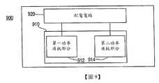
根據本發明之又一實施例,提供一種無線耳機系統,其包括處理器電路及配電電路。處理器電路可包括第一功率消耗部分及第二功率消耗部分。配電電路可操作以獨立於第二功率消耗部分是否被供電而選擇性對第一功率消耗部分供電。According to another embodiment of the present invention, a wireless earphone system is provided, which includes a processor circuit and a power distribution circuit. The processor circuit may include a first power consumption part and a second power consumption part. The power distribution circuit is operable to selectively control the second power consuming part independently of whether the second power consuming part is powered or not.A power consumption part supplies power.
10:耳機10: Headphones
11:主外殼11: main shell
12:耳芽12: Ear buds
13:揚聲器系統13: speaker system
14:按鈕14: Button
15:天線15: Antenna
16:連接器16: connector
17:麥克風17: Microphone
18:顯示系統18: display system
19:電池19: battery
20:處理器20: processor
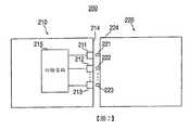
200:耳機連接器系統200: Headphone connector system
210:耳機210: Headphone
211:耳機連接器接觸區域211: Headphone connector contact area
212:耳機連接器接觸區域212: Headphone connector contact area
213:耳機連接器接觸區域213: Headphone connector contact area
214:面部214: Face
215:切換電路215: switching circuit
220:耳機嚙合連接器220: Headphone engagement connector
221:耳機嚙合接觸區域221: Headphone engagement contact area
222:耳機嚙合接觸區域222: Headphone engagement contact area
223:耳機嚙合接觸區域223: Headphone engagement contact area
224:外殼224: Shell
300:電子器件300: electronic devices
310:外殼310: Shell
320:連接器總成320: connector assembly
321:觸點321: Contact
322:埠322: Port
323:觸點323: Contact
324:麥克風324: Microphone
325:觸點325: Contact
326:通道326: Channel
327:觸點327: Contact
400:電子器件400: electronic devices
410:外殼410: Shell
420:麥克風總成420: Microphone assembly
430:麥克風430: Microphone
432:麥克風埠432: Microphone port
440:麥克風罩440: Microphone cover
450:連接器板450: connector board
451:觸點451: Contact
452:連接器埠452: connector port
453:觸點453: Contact
455:觸點455: Contact
457:觸點457: Contact
500:耳機500: headphones
510:主外殼510: main shell
512:主外殼可撓性電路板512: Flexible circuit board for main housing
514:麥克風514: Microphone
520:耳芽520: Ear Buds
522:耳芽可撓性電路板522: Ear Bud Flexible Circuit Board
524:接收器524: Receiver
526:處理電路526: Processing Circuit
600:耳機器件600: Headphone device
610:耳芽外殼610: Ear Bud Shell
612:耳芽通孔612: Ear Bud Through Hole
614:頸嚙合表面614: neck engagement surface
620:螺紋頸620: threaded neck
622:第一頸表面622: first neck surface
624:第二頸表面624: second neck surface
630:主外殼630: main shell
632:主外殼通孔632: Main housing through hole
634:頸嚙合表面634: neck engagement surface
690:螺桿690: Screw
692:中空通道692: Hollow Channel
694:特徵694: Feature
700:顯示系統700: display system
710:外殼710: Shell
712:信號指示器區域712: Signal indicator area
714:內部壁714: inner wall
720:光源720: light source
730:擴散器730: diffuser
740:控制電路740: control circuit
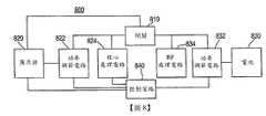
800:配電系統800: power distribution system
810:開關810: switch
820:匯流排820: Bus
822:第一功率調節電路822: The first power regulation circuit
824:核心處理電路824: core processing circuit
830:電池830: battery
832:第二功率調節電路832: second power regulation circuit
834:RF處理電路834: RF processing circuit
840:控制電路840: control circuit
900:無線耳機900: wireless headphones
910:處理器電路910: processor circuit
912:第一功率消耗部分912: The first power consumption part
914:第二功率消耗部分914: The second power consumption part
920:配電電路920: Power Distribution Circuit
1000:耳機1000: headphones
1010:主外殼1010: main shell
1011:天線蓋1011: Antenna cover
1012:按鈕1012: Button
1013:顯示器1013: display
1020:耳芽1020: ear buds
1021:聲學埠1021: Acoustic Port
1022:聲學埠1022: Acoustic Port
1030:頸1030: neck
1040:連接器1040: Connector
1041:凹入連接器板1041: Recessed connector board
1042:觸點1042: Contact
1100:耳機1100: Headphones
1110:主外殼1110: main shell
1111:天線蓋1111: Antenna cover
1112:按鈕1112: Button
1113:電子組件1113: electronic components
1115:主外殼電路板1115: main housing circuit board
1116:托架1116: bracket
1117:附件1117: Accessories
1118:天線1118: Antenna
1119:電池組1119: battery pack
1120:耳芽外殼1120: ear bud shell
1122:耳芽電路板1122: Ear Bud Circuit Board
1123:處理器1123: processor
1124:接收器1124: receiver
1130:頸1130: neck
1131:螺桿部件1131: Screw parts
1132:螺桿部件1132: Screw parts
1140:連接器1140: Connector
1141:連接器板1141: connector board
1142:觸點1142: Contact
1143:套管1143: Casing
1144:麥克風罩1144: Microphone cover
1200:耳機1200: Headphones
1210:主外殼1210: main shell
1212:壁1212: wall
1217:按鈕導引1217: button guidance
1218:天線1218: Antenna
1240:連接器1240: Connector
1242:突出1242: prominent
1244:光擴散器1244: light diffuser
1300:藍芽協定堆疊1300: Bluetooth Protocol Stack
1302:下部堆疊1302: lower stack
1304:主機控制介面1304: Host control interface
1306:延伸同步連接導向1306: Extend the synchronization connection guide
1308:邏輯連接控制及適應協定1308: Logical connection control and adaptation protocol
1310:RFCOMM1310: RFCOMM
1312:服務發現協定1312: Service Discovery Agreement
1314:框架1314: frame
1316:應用程式層1316: application layer
1400:電子系統1400: Electronic System
1410:處理器電路1410: processor circuit
1411:處理器1411: processor
1412:接收器1412: receiver
1413:重設電路1413: Reset circuit
1414:功率場效應電晶體(FET)1414: Power Field Effect Transistor (FET)
1415:天線1415: Antenna
1416:通用異步收發器(UART)多工器1416: Universal Asynchronous Receiver Transmitter (UART) multiplexer
1420:介面電路1420: Interface circuit
1421:麥克風隔離低壓降調節器(LDO)1421: Microphone isolation low-dropout regulator (LDO)
1422:微機電(MEMs)麥克風1422: Microelectromechanical (MEMs) microphone
1423:開關1423: switch
1424:LED驅動器1424: LED driver
1430:配電電路1430: power distribution circuit
1431:過壓保護及保險絲1431: Overvoltage protection and fuse
1432:電池保護電路1432: battery protection circuit
1433:熱敏電阻1433: Thermistor
1440:切換電路1440: switching circuit
1441:電力極性切換電路1441: Power polarity switching circuit
1442:資料極性切換電路1442: Data polarity switching circuit
1450:4插腳對稱磁性連接器1450: 4-pin symmetrical magnetic connector
1500:處理器1500: processor
1510:振盪器1510: Oscillator
1511:時脈產生電路1511: Clock generation circuit
1520:RF電路1520: RF circuit
1530:基頻電路1530: Fundamental frequency circuit
1531:快閃記憶體1531: flash memory
1532:隨機存取記憶體(RAM)1532: Random Access Memory (RAM)
1533:微處理器1533: Microprocessor
1540:全速USB控制器1540: Full-speed USB controller
1541:UART電路1541: UART circuit
1550:音訊編解碼器(CODEC)1550: Audio Codec (CODEC)
1551:輸入放大器1551: input amplifier
1552:輸出放大器1552: output amplifier
1560:功率控制及調節電路1560: Power control and regulation circuit
1561:LDO1561: LDO
1562:電池充電器1562: battery charger
1563:開關模式電源(SMPS)1563: Switch Mode Power Supply (SMPS)
1570:可程式化I/O1570: Programmable I/O
1571:LED驅動器1571: LED driver
1572:類比數位轉換器(ADC)1572: Analog to Digital Converter (ADC)
1600:配電系統1600: Power Distribution System
1605:處理器1605: processor
1610:核心電路1610: core circuit
1611:輸出線1611: output line
1612:輸出線1612: output line
1613:輸出線1613: output line
1614:輸入線1614: input line
1615:無線電電路1615: radio circuit
1620:LDO1620: LDO
1625:SMPS1625: SMPS
1630:類比數位轉換器(ADC)1630: Analog-to-digital converter (ADC)
1631:邏輯閘1631: Logic Gate
1632:邏輯閘1632: Logic Gate
1633:節點1633: Node
1640:功率FET1640: Power FET
1641:節點1641: Node
1642:節點1642: Node
1650:匯流排(BUS)1650: Bus (BUS)
1655:BAT1655: BAT
1660:按鈕1660: Button
1661:邏輯閘1661: Logic Gate
1790:電路板1790: circuit board
1792:處理器1792: processor
1796:電組件1796: electrical components
1800:系統1800: System
1810:電路板1810: circuit board
1812:藍芽處理器1812: Bluetooth processor
1814:平衡RF濾波器電路1814: Balanced RF filter circuit
1820:電路板1820: circuit board
1821:RF匹配電路1821: RF matching circuit
1822:天線1822: antenna
1823:介面電路1823: interface circuit
1824:配電電路1824: power distribution circuit
1825:切換電路1825: switching circuit
1826:4插腳對稱磁性連接器1826: 4-pin symmetrical magnetic connector
1830:同軸電纜1830: Coaxial cable
1832:匯流排1832: bus
1920:耳芽電路板1920: ear bud circuit board
1921:連接器引線1921: Connector leads
1922:處理器1922: processor
1923:剛性區段1923: rigid section
1924:接收器1924: receiver
1925:剛性區段1925: rigid section
1926:電子組件1926: electronic components
1927:剛性區段1927: rigid section
1928:連接器1928: Connector
1990:電路板1990: circuit board
1992:處理器1992: processor
1996:組件1996: components
2000:耳機2000: Headphones
2010:主外殼2010: main enclosure
2011:主外殼電路板2011: main housing circuit board
2012:空腔2012: cavity
2013:耳機頸2013: Headphone neck
2014:耳芽2014: ear buds
2018:連接器2018: Connector
2020:耳芽電路板2020: Ear Bud Circuit Board
2021:連接器引線2021: connector leads
2022:處理器2022: processor
2023:剛性區段2023: rigid section
2024:接收器2024: receiver
2025:中間剛性區段2025: Intermediate rigid section
2026:電子組件2026: electronic components
2027:頂部剛性區段2027: Top rigid section
2028:連接器2028: Connector
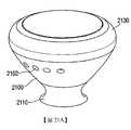
2100:耳芽外殼2100: ear bud shell
2102:聲學埠2102: Acoustic Port
2110:頸2110: neck
2112:螺桿2112: screw
2120:電路板2120: circuit board
2123:底部密封墊2123: bottom gasket
2124:接收器2124: receiver
2127:區段2127: section
2130:帶槽框2130: slotted frame
2131:篩2131: Sieve
2132:篩2132: Sieve
2134:頂部密封墊2134: top gasket
2135:托架2135: Bracket
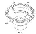
2200:外殼2200: Shell
2202:聲學埠2202: Acoustic Port
2204:篩網2204: Screen
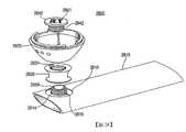
2300:耳芽外殼2300: ear bud shell
2327:剛性區段2327: rigid section
2328:聲學埠2328: Acoustic Port
2427:電路板區段2427: Circuit board section
2428:聲學埠2428: Acoustic Port
2430:聲學篩網2430: Acoustic screen
2440:底部密封墊2440: bottom gasket
2441:發泡體2441: foam
2530:帶槽框2530: slotted frame
2531:篩2531: Sieve
2533:聲學埠2533: Acoustic Port
2534:密封墊2534: gasket
2536:輪緣2536: Flange
2620:接收器2620: receiver
2622:彈簧觸點2622: Spring contact
2623:尖端2623: tip
2624:彈簧觸點2624: Spring contact
2625:尖端2625: tip
2630:帶槽框2630: slotted frame
2636:輪緣2636: Flange
2700:耳芽外殼2700: ear bud shell
2702:聲學埠2702: Acoustic Port
2710:頸2710: neck
2712:插入物2712: Insert
2716:內腔2716: inner cavity
2720:電路板2720: circuit board
2724:接收器2724: receiver
2725:中間剛性區段2725: Intermediate rigid section
2727:頂部剛性區段2727: Top rigid section
2728:聲學埠2728: Acoustic Port
2729:可撓性區段2729: Flexible section
2730:帶槽框2730: slotted frame
2731:篩2731: Sieve
2732:篩2732: Sieve
2733:音訊埠2733: Audio port
2734:頂部密封墊2734: top gasket
2736:輪緣2736: Flange
2738:凹口及肋狀物組態2738: Notch and rib configuration
2740:底部密封墊2740: bottom gasket
2750:同軸電纜2750: Coaxial cable
2752:連接器2752: Connector
2754:暴露部分2754: exposed part
2760:導電制動器2760: conductive brake
2792:前部體積2792: front volume
2794:接收器體積、聲學體積2794: receiver volume, acoustic volume
2796:後部耳芽體積、聲學體積2796: Rear ear bud volume, acoustic volume
2798:外部環境2798: external environment
2800:附接系統2800: Attach system
2810:主外殼2810: main shell
2814:通孔2814: Through hole
2816:槽2816: slot
2818:凹入區域2818: recessed area
2820:耳芽外殼2820: ear bud shell
2830:頸2830: neck
2831:突起2831: protrusion
2840:插入物2840: Insert
2841:特徵2841: Features
2842:螺紋2842: Thread
2850:插入物2850: Insert
3000:定製工具3000: Custom tools
3010:部件3010: parts
3011:附件3011: accessories
3012:塑膠覆蓋物3012: plastic covering
3013:脊3013: Ridge
3014:機械臂3014: Robotic Arm
3015:較窄區段3015: Narrower section
3016:尖端3016: tip
3017:外向突出3017: Outward protrusion
3020:部件3020: parts
3021:附件3021: Accessories
3022:塑膠覆蓋物3022: plastic covering
3023:脊3023: Ridge
3024:機械臂3024: Robotic Arm
3025:較窄區段3025: narrower section
3026:尖端3026: tip
3027:外向突出3027: Outward protrusion
3030:緊固件3030: Fasteners
3040:彈簧3040: spring
3090:頸3090: neck
3092:主外殼3092: main housing
3100:管3100: Tube
3102:壁厚度3102: wall thickness
3104:內部壁3104: inner wall
3106:厚度3106: thickness
3108:厚度3108: thickness
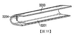
3200:管3200: Tube
3201:內表面3201: inner surface
3202:壁厚度、管厚度3202: wall thickness, tube thickness
3204:內部壁3204: inner wall
3400:管3400: Tube
3401:內表面3401: inner surface
3402:最終厚度3402: final thickness
3403:長度3403: length
3404:內部壁3404: inner wall
3410:模3410: mold
3412:模末端3412: die end
3420:壓模3420: die
3422:厚度3422: thickness
3430:表面3430: Surface
3700:管3700: tube
3701:內表面3701: inner surface
3702:厚度3702: thickness
3704:內部壁3704: inner wall
3710:表面3710: Surface
3722:材料3722: material
3730:表面3730: Surface
3900:管3900: tube
3901:周圍內部表面3901: Surrounding internal surface
3902:厚度3902: thickness
3904:內部壁3904: inner wall
3906:厚度3906: thickness
3908:高度3908: height
3910:第一壓痕3910: first indentation
3912:表面3912: surface
3914:第二壓痕3914: second indentation
3916:表面3916: Surface
3921:周圍內部表面3921: Surrounding internal surface
3922:厚度3922: thickness
3930:表面3930: Surface
4100:管4100: Tube
4101:內表面4101: inner surface
4102:厚度4102: thickness
4104:內壁壁4104: inner wall
4110:壓痕4110: Indentation
4112:平面4112: Plane
4114:壓痕4114: Indentation
4122:壁厚度4122: wall thickness
4124:材料4124: Material
4130:表面4130: Surface
4800:視覺指示器系統4800: Visual indicator system
4810:外殼4810: shell
4812:微穿孔4812: Micro perforation
4814:外部孔4814: External hole
4816:內部孔4816: internal hole
4820:電路板4820: circuit board
4821:光源4821: light source
4822:光源4822: light source
4830:擴散器4830: diffuser
4832:外部核心4832: external core
4834:內部核心4834: internal core
4835:透明或半透明基板4835: Transparent or translucent substrate
4836:擴散微粒4836: Diffusion Particles
4860:光4860: light
4862:光4862: light
4890:寬度4890: width
4892:寬度4892: width
4910:耳機4910: Headphones
4912:微穿孔4912: Micro perforation
4913:視覺指示器4913: visual indicator
4921:LED4921: LED
4922:LED4922: LED
4990:直徑4990: Diameter
5000:耳機5000: headphones
5010:主外殼5010: main housing
5040:連接器5040: Connector
5041:連接器板5041: connector board
5042:槽5042: slot
5043:觸點5043: Contact
5044:套管5044: Casing
5050:麥克風埠5050: Microphone port
5090:寬度5090: width
5092:高度5092: height
5115:主外殼電路板5115: main housing circuit board
5120:麥克風罩5120: Microphone cover
5140:連接器5140: Connector
5141:連接器板5141: connector board
5143:觸點5143: Contact
5144:隨附套管5144: Supplied with sleeve
5150:麥克風埠5150: Microphone port
5200:連接器5200: Connector
5215:電路板5215: circuit board
5220:麥克風罩5220: Microphone cover
5222:麥克風5222: Microphone
5240:連接器板5240: connector board
5243:觸點5243: Contact
5244:套管5244: casing
5248:托架5248: Bracket
5249:螺桿5249: Screw
5320:麥克風罩5320: Microphone cover
5325:孔5325: hole
5326:密封表面5326: sealing surface
5327:頂5327: top
5420:麥克風罩5420: Microphone cover
5421:麥克風輸入5421: Microphone input
5422:麥克風5422: Microphone
5425:罩孔5425: hood hole
5426:表面5426: Surface
5428:栓塞5428: embolism
5440:連接器板5440: connector board
5445:表面5445: Surface
5450:麥克風埠5450: Microphone port
5490:接縫5490: Seam
5500:耳機5500: headphones
5510:主外殼5510: main shell
5540:連接器板5540: connector board
5542:凹入槽5542: recessed slot
5561:觸點5561: Contact
5562:觸點5562: Contact
5563:觸點5563: Contact
5564:觸點5564: Contact
5580:高度5580: height
5581:高度5581: height
5582:高度5582: height
5583:間距5583: Spacing
5584:寬度5584: width
5585:尺寸5585: size
5586:寬度5586: width
5587:角5587: angle
5588:高度5588: height
5589:深度5589: Depth
5590:寬度5590: width
5591:寬度5591: width
5592:寬度5592: width
5601:總成5601: assembly
5602:電觸點5602: electrical contacts
5603:套管5603: Casing
5604:電觸點5604: electrical contacts
5605:電路板5605: circuit board
5690:深度5690: Depth
5701:總成5701: assembly
5702:電觸點5702: electrical contacts
5703:不導電套管5703: Non-conductive sleeve
5704:第二部分5704: Part Two
5705:第一部分5705: Part One
5706:頭5706: head
5707:桿5707: Rod
5708:接觸段5708: contact segment
5709:嚙合段5709: meshing section
5801:總成5801: assembly
5802:電觸點5802: electrical contacts
5803:套管5803: Casing
5804:第二部分5804: Part Two
5805:第一部分5805: Part One
5806:嚙合段5806: meshing section
5807:桿5807: pole
5808:接觸段5808: contact segment
5809:薄片金屬5809: sheet metal
5810:指狀物5810: finger
5901:電觸點5901: electrical contacts
5902:外部接觸部分5902: External contact part
5903:桿5903: Rod
5904:內部接觸部分5904: Internal contact part
5905:電觸點5905: electrical contacts
5906:外部接觸部分5906: External contact part
5907:桿5907: Rod
5908:內部接觸部分5908: Internal contact part
6040:連接器板6040: connector board
6042:凹入臺階6042: recessed steps
6045:表面6045: Surface
6046:螺紋空腔6046: Threaded cavity
6047:突出6047: prominent
6050:麥克風埠6050: Microphone port
6051:空腔6051: cavity
6140:連接器板6140: connector board
6180:陣列6180: Array
6181:組件6181: components
6182:組件6182: components
6183:組件6183: components
6184:組件6184: components
6185:組件6185: components
6186:配合面6186: Mating surface
6200:連接器6200: Connector
6210:連接器外殼6210: Connector shell
6212:升高面6212: raised surface
6214:凹入周邊6214: recessed into the periphery
6280:陣列6280: Array
6281:磁性組件6281: Magnetic components
6282:組件6282: components
6283:組件6283: Components
6284:組件6284: components
6285:磁性組件6285: Magnetic components
6286:配合面6286: Mating surface
6290:觸點6290: Contact
6291:線圈6291: Coil
6292:觸點6292: Contact
6293:線圈6293: Coil
6294:觸點6294: Contact
6295:線圈6295: coil
6296:觸點6296: Contact
6297:線圈6297: Coil
6300:連接器6300: Connector
6301:寬度6301: width
6302:間距6302: Spacing
6303:寬度6303: width
6304:總高度6304: total height
6305:高度6305: height
6306:距離6306: distance
6310:外殼6310: shell
6312:升高面6312: Raised surface
6382:磁性組件6382: Magnetic components
6383:磁性組件6383: Magnetic components
6384:磁性組件6384: Magnetic components
6390:觸點尖端6390: contact tip
6392:觸點尖端6392: Contact tip
6394:觸點尖端6394: Contact tip
6396:觸點尖端6396: Contact tip
6400:基座台6400: Pedestal table
6401:箭頭6401: Arrow
6402:箭頭6402: Arrow
6412:升高面6412: raised surface
6414:周邊6414: Peripheral
6480:電路板6480: circuit board
6490:觸點6490: Contact
6491:線圈6491: coil
6498:耳機6498: Headphones
6499:連接器6499: Connector
6500:圖表6500: chart
6502:x軸6502: x axis
6504:y軸6504: y axis
6506:近似磁力6506: Approximate magnetic force
6508:近似力6508: Approximate force
6600:充電器件6600: charging device
6601:連接器6601: Connector
6610:輔助連接器6610: auxiliary connector
6620:電纜6620: cable
6630:電路6630: Circuit
6700:基座台6700: Pedestal table
6702:空腔6702: cavity
6704:空腔6704: cavity
6710:連接器6710: Connector
6711:尖峰6711: Spike
6712:升高面6712: Raised surface
6714:凹入周邊6714: recessed into the periphery
6720:耳機6720: Headphones
6721:較長側6721: Longer side
6800:圖表6800: chart
6810:行6810: OK
6811:來電模式6811: Incoming call mode
6812:應答呼叫功能6812: Answer call function
6813:拒絕呼叫功能6813: Reject call function
6814:功能6814: function
6820:行6820: OK
6830:行6830: OK
6840:行6840: OK
6850:行6850: OK
圖1為根據本發明之實施例之耳機的簡化方塊圖;圖2為根據本發明之實施例之耳機連接器系統的簡化方塊圖;圖3為根據本發明之實施例之連接器總成的簡化橫截面說明;圖4為根據本發明之實施例之另一連接器總成的簡化橫截面說明;圖5為根據本發明之實施例之耳機的簡化方塊圖;圖6A為根據本發明之實施例之耳機的一部分之簡化橫截面說明;圖6B為根據本發明之實施例之螺桿的簡化橫截面說明;圖7為根據本發明之實施例之顯示系統的簡化方塊圖;圖8為根據本發明之實施例之配電系統的簡化方塊圖;圖9為根據本發明之實施例之另一配電系統的簡化方塊圖;圖10A及圖10B為根據本發明之實施例之耳機的說明;圖11為根據本發明之實施例之耳機的分解圖;圖12為根據本發明之另一實施例之耳機的分解圖;圖13為根據本發明之實施例之展示藍芽器件中之軟體如何組織的簡化圖;圖14為根據本發明之實施例之耳機的電系統之簡化方塊圖;圖15為根據本發明之實施例之耳機的核心處理器之簡化方塊圖;圖16為根據本發明之實施例之配電系統的簡化示意圖;圖17A至圖17C為傳統電路板及耳機中之電組件之分布的說明;圖18為具有根據本發明之實施例之耳機中電組件的改良分布之電路板之簡化方塊圖;圖19A及圖19B為將圖7A至圖7C之傳統電路板與具有根據本發明之實施例的耳機中電組件之改良分布之電路板比較的說明;圖20A至圖20C為根據本發明之實施例之耳機中電組件的改良分布之說明;圖21A為根據本發明之實施例之耳機耳芽的說明;圖21B為根據本發明之實施例之耳機耳芽的簡化分解圖;圖22至圖25及圖26A為根據本發明之一些實施例之處於各種裝配狀態的耳機耳芽之簡化說明;圖26B為根據本發明之實施例之音訊接收器的簡化橫截面圖;圖27A為根據本發明之實施例之部分裝配的耳機耳芽之簡化橫截面圖;圖27B為根據本發明之實施例之完全裝配的耳機耳芽之簡化橫截面圖;圖28為根據本發明之實施例之附接系統的分解圖;圖29為根據本發明之實施例用於裝配耳機之部分的說明性過程之流程圖。Figure 1 is a simplified block diagram of an earphone according to an embodiment of the present invention; Figure 2 is a simplified block diagram of an earphone connector system according to an embodiment of the present invention; Figure 3 is a simplified block diagram of a connector assembly according to an embodiment of the present invention Simplified cross-sectional description; Fig. 4 is a simplified cross-sectional description of another connector assembly according to an embodiment of the present invention; Fig. 5 is a simplified block diagram of an earphone according to an embodiment of the present invention; Fig. 6A is a simplified block diagram of an earphone according to an embodiment of the present invention; A simplified cross-sectional description of a part of the earphone of the embodiment; FIG. 6B is a simplified cross-sectional description of the screw according to the embodiment of the present invention; FIG. 7 is a simplified block diagram of the display system according to the embodiment of the present invention; A simplified block diagram of a power distribution system according to an embodiment of the present invention; FIG. 9 is a simplified block diagram of another power distribution system according to an embodiment of the present invention; FIGS. 10A and 10B are illustrations of a headset according to an embodiment of the present invention; 11 is an exploded view of a headset according to an embodiment of the present invention; FIG. 12 is an exploded view of a headset according to another embodiment of the present invention; FIG. 13 is a diagram showing how the software in a Bluetooth device is organized according to an embodiment of the
圖30A及圖30B為根據本發明之實施例可用於輔助裝配耳機的一部分之工具的說明;圖30C為根據本發明之實施例使用之圖30A及圖30B的工具之說明;圖31為根據本發明之實施例之"完成"管的橫截面圖;圖32為根據本發明之實施例之初始製造的管之橫截面圖;圖33為根據本發明之實施例之圖31的管之橫截面之透視圖;圖34為根據本發明之實施例用於修改圖32的初始製造之管之說明性模及壓模;圖35為根據本發明之實施例圖34之管在一旦自管移除壓模及模時的橫截面圖;圖36為根據本發明之實施例圖35之管在一旦管經加工以產生內部壁時之透視圖;圖37為根據本發明之實施例使用單一衝擠形成之說明性管的橫截面圖;圖38為根據本發明之實施例圖37之管在一旦管經加工以產生內部壁時之透視圖;圖39為根據本發明之實施例使用雙衝擠形成之說明性管的橫截面圖;圖40為根據本發明之實施例圖39之管在一旦管經加工以產生內部壁時之透視圖;圖41為根據本發明之實施例使用級進式深拉過程形成之說明性管的橫截面圖。Figures 30A and 30B are illustrations of tools that can be used to assist in assembling a part of the headset according to an embodiment of the present invention; Figure 30C is an illustration of the tools of Figures 30A and 30B used in accordance with an embodiment of the present invention; Figure 31 is an illustration of tools according to the present invention A cross-sectional view of the "finished" tube of an embodiment of the invention; FIG. 32 is a cross-sectional view of an initially manufactured tube according to an embodiment of the present invention; FIG. 33 is a cross-section of the tube of FIG. 31 according to an embodiment of the present invention A perspective view; FIG. 34 is an illustrative diagram for modifying the initially manufactured tube of FIG. 32 according to an embodiment of the present inventionDie and die; Figure 35 is a cross-sectional view of the tube once the die and die are removed from the tube according to an embodiment of the present invention; Figure 36 is an embodiment of the present invention. A perspective view when processed to produce an inner wall; FIG. 37 is a cross-sectional view of an illustrative tube formed using a single extrusion according to an embodiment of the present invention; FIG. 38 is an embodiment of the present invention. A perspective view when processed to produce an inner wall; FIG. 39 is a cross-sectional view of an illustrative tube formed using double stamping according to an embodiment of the present invention; FIG. 40 is an embodiment of the present invention. A perspective view when processed to produce the inner wall; FIG. 41 is a cross-sectional view of an illustrative tube formed using a progressive deep drawing process according to an embodiment of the present invention.
圖42為根據本發明之實施例之圖41的管之橫截面之透視圖;圖43為根據本發明之實施例圖41及圖42之管在一旦管經加工以產生內部壁時之透視圖;圖44為根據本發明之實施例使用模及壓模來形成具有位於管的內部表面上之特徵之擠壓管的說明性過程之流程圖;圖45為根據本發明之實施例使用單一衝擠來形成具有位於管的內部表面上之特徵之管的說明性過程之流程圖;圖46為根據本發明之實施例在管之兩個末端上使用衝擠而形成具有位於管的內部表面上之特徵之管的說明性過程之流程圖;圖47為根據本發明之實施例使用級進式深拉過程形成具有位於管的內部表面上之特徵之管的說明性過程之流程圖;圖48為根據本發明之實施例之視覺指示器系統的橫截面圖;圖49為根據本發明之實施例之耳機的視覺指示器系統之說明;圖50A及圖50B為根據本發明之實施例之耳機的說明;圖51為根據本發明之實施例之連接器的說明;圖52為根據本發明之實施例之連接器的分解圖;圖53為根據本發明之實施例之麥克風罩的說明;圖54為根據本發明之實施例之連接器的橫截面圖;圖55A至圖55D為根據本發明之實施例之耳機的說明;圖56為根據本發明之實施例耦接至電路板之電觸點總成的橫截面圖;圖57A及圖57B為根據本發明之實施例之電觸點總成的說明;圖58A至圖58C為根據本發明之實施例之電觸點總成的說明;圖59A及圖59B為根據本發明之實施例之電觸點的說明;圖60A及圖60B為根據本發明之實施例之連接器板的說明;圖61A及圖61B為根據本發明之實施例之連接器的磁性組件之說明;圖62A及圖62B為根據本發明之實施例之連接器的說明;圖63A及圖63B為根據本發明之實施例之連接器的說明;圖64為根據本發明之實施例與互補連接器耦接之耳機的說明;圖65為根據本發明之實施例之耳機與互補連接器的耦接中所涉及之磁力及彈簧力之簡化圖表;圖66為可接收根據本發明之實施例之耳機的基座器件之說明;圖67A為根據本發明之實施例之連接器的說明;圖67B為根據本發明之實施例與互補連接器耦接之耳機的說明;及圖68為列舉根據本發明之實施例之通信系統的例示性模式及功能之圖表。42 is a perspective view of a cross-section of the tube of FIG. 41 according to an embodiment of the present invention; FIG. 43 is a perspective view of the tube of FIGS. 41 and 42 once the tube is processed to produce an inner wall according to an embodiment of the present invention Fig. 44 is a flowchart of an illustrative process of using a mold and a die to form an extruded tube with features located on the inner surface of the tube according to an embodiment of the present invention; Fig. 45 is a flow chart of an illustrative process using a single punch according to an embodiment of the present invention A flow chart of an illustrative process of extrusion to form a tube with features located on the inner surface of the tube; FIG. 46 is a flow chart showing the use of extrusion on both ends of the tube according to an embodiment of the present invention to form a tube withA flowchart of an illustrative process for a tube with features located on the inner surface of the tube; FIG. 47 is an illustrative process for forming a tube with features on the inner surface of the tube using a progressive deep drawing process according to an embodiment of the present invention Figure 48 is a cross-sectional view of a visual indicator system according to an embodiment of the present invention; Figure 49 is an illustration of a headset visual indicator system according to an embodiment of the present invention; Figures 50A and 50B are based on this Description of the earphone of the embodiment of the invention; FIG. 51 is a description of the connector according to the embodiment of the present invention; FIG. 52 is an exploded view of the connector according to the embodiment of the present invention; FIG. 53 is the embodiment of the connector according to the present invention Description of the microphone cover; Fig. 54 is a cross-sectional view of the connector according to an embodiment of the present invention; Figs. 55A to 55D are descriptions of a headset according to an embodiment of the present invention; Fig. 56 is a coupling according to an embodiment of the present invention A cross-sectional view of the electrical contact assembly to the circuit board; FIGS. 57A and 57B are illustrations of the electrical contact assembly according to an embodiment of the present invention; FIGS. 58A to 58C are electrical contacts according to an embodiment of the present invention Description of the point assembly; Figs. 59A and 59B are descriptions of electrical contacts according to an embodiment of the present invention; Figs. 60A and 60B are descriptions of a connector board according to an embodiment of the present invention; Figs. 61A and 61B are Description of the magnetic component of the connector according to the embodiment of the present invention; Figure 62A and Figure 62B are the description of the connector according to the embodiment of the present invention; Figures 63A and 63B are the description of the connector according to the embodiment of the present invention Figure 64 is an illustration of a headset coupled with a complementary connector according to an embodiment of the present invention; Figure 65 is a simplified diagram of the magnetic force and spring force involved in the coupling of the headset and the complementary connector according to an embodiment of the present invention ;FIG. 66 is an illustration of a base device that can receive an earphone according to an embodiment of the present invention; FIG. 67A is an illustration of a connector according to an embodiment of the present invention; FIG. 67B is an embodiment of the present invention coupled to a complementary connector Description of the headset; and FIG. 68 is a chart enumerating exemplary modes and functions of the communication system according to an embodiment of the present invention.
本發明係關於耳機及其製造方法。耳機為佩帶於使用者之頭部以便允許與諸如電腦、電話耳機、蜂巢式電話、汽車及/或類似物之主機器件的免持資料及/或語音通信之通信器件。耳機可包括用於音訊輸出之一或多個揚聲器(接近一隻或兩隻耳朵)及/或用於音訊輸入之一或多個麥克風。The present invention relates to earphones and manufacturing methods thereof. A headset is a communication device that is worn on the head of a user to allow hands-free data and/or voice communication with host devices such as computers, telephone headsets, cellular phones, automobiles, and/or the like. The headset may include one or more speakers (near one or both ears) for audio output and/or one or more microphones for audio input.
耳機可以各種外形尺寸或形狀出現。在一些狀況下,耳機可具體化為充當用於佩帶耳機之主支撐機構之聽筒。舉例而言,耳機可藉由佩帶於耳朵上或耳朵中之聽筒支撐於頭部上。或者,耳機可藉由配合於使用者頭部上之框架或帶支撐。耳機可包括將麥克風置於較接近使用者嘴部(圍繞臉部)處之固定或可移動吊桿。或者,耳機可無吊桿,使得麥克風與聽筒整合,進而形成較緊密之器件(例如,較小、較輕、較美觀等)。Headphones can appear in various dimensions or shapes. In some cases, the earphone can be embodied as an earpiece that serves as the main support mechanism for wearing the earphone. For example, the earphone can be supported on the head by a handset worn on or in the ear. Alternatively, the earphone can be supported by a frame or strap that fits on the user's head. The headset may include a fixed or movable boom that places the microphone closer to the user's mouth (around the face). Or, the earphone can be without a boom, so that the microphone and the earpiece are integrated to form a compact device (for example, smaller, lighter, more beautiful, etc.).
根據本發明之一態樣,耳機可具體化為小緊密單元,其包括主外殼及自其延伸之耳芽部件。耳芽部件可附接至主外殼或與其形成為一體。各種組件可置於耳芽部件及主外殼之邊界之表面處或內部。實際上,兩者可視器件之需要而包括一或多個組件。含於其中之每一者內之組件可廣泛變化。操作組件之實例可包括揚聲器、麥克風、天線、連接器、按鈕、顯示器、指示器、電池及相關聯之處理器、控制器及電路。通常,耳芽部件包括至少一揚聲器,而主外殼包括至少一麥克風(儘管此並非要求)。視其大小而定,此等部件中之每一者可包括耳機之額外組件。在一個實施例中,主外殼包括天線、使用者介面按鈕、指示器或顯示器(例如,LED)、電池、麥克風及/或連接器以及任何隨附電路,而揚聲器、處理器及其隨附電路可位於耳芽中。按鈕可位於主外殼之一個末端上。使用者可與此按鈕建立介面以執行各種功能(例如,終止呼叫)。According to one aspect of the present invention, the earphone can be embodied as a small compact unit, which includes a main housing and an ear bud part extending therefrom. The ear bud part may be attached to the main housing or formed integrally therewith. Various components can be placed on or inside the boundary between the ear bud part and the main housing. In fact, both may include one or more components depending on the needs of the device. The components contained in each of them can vary widely. Examples of operating components may include speakers, microphones, antennas, connectors, buttons, displays, indicators, batteries, and associated processors, controllers, and circuits. Generally, the ear bud component includes at least one speaker, and the main housing includes at least one microphone (although this is not a requirement). Regarding the sizeDepending on the size, each of these components may include additional components of the headset. In one embodiment, the main housing includes an antenna, user interface buttons, indicators or displays (e.g., LEDs), batteries, microphones and/or connectors, and any accompanying circuits, and speakers, processors and accompanying circuits Can be located in ear buds. The button can be located on one end of the main housing. The user can create an interface with this button to perform various functions (for example, terminate a call).
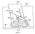
耳芽部件及主外殼之形狀及大小及定向可廣泛變化。在一個實施例中,耳芽部件經組態用於插入耳朵中,使得其支撐耳機之接近使用者之頭部的剩餘部分(例如,主外殼)。在一個實施例中,主外殼可經組態為縱向部件(例如,管)。在一個實例中,含有揚聲器之耳芽部件自縱向延伸之主外殼的一個末端垂直突出,縱向延伸之主外殼包括位於縱向延伸之主外殼的相對末端處之麥克風。此外,耳芽部件可向外擴展且接著自耦接至主外殼之頸部分向內擴展,以便形成配合入耳朵中之芽部。The shape, size and orientation of the ear bud components and the main housing can vary widely. In one embodiment, the ear bud component is configured to be inserted into the ear so that it supports the remaining part of the earphone close to the user's head (e.g., the main housing). In one embodiment, the main housing may be configured as a longitudinal member (e.g., a tube). In one example, the ear bud member containing the speaker protrudes vertically from one end of the longitudinally extending main housing, and the longitudinally extending main housing includes microphones located at the opposite ends of the longitudinally extending main housing. In addition, the ear bud part can expand outwardly and then expand inwardly from the neck portion coupled to the main housing, so as to form a bud part that fits into the ear.
主外殼可包括形成外殼並經由開放末端收納內部組件之管。管可使用若干過程中之一者製造以便降低成本及增加速度及效率。在一個實施例中,管可經製造以包括位於管之內表面上用於支撐耳機之電子組件的特徵。用於產生此管之過程可包括對擠壓管應用模及模壓、單一或雙衝擠、或級進式深拉過程。The main housing may include a tube forming the housing and receiving internal components through the open end. The tube can be manufactured using one of several processes in order to reduce cost and increase speed and efficiency. In one embodiment, the tube may be manufactured to include features on the inner surface of the tube for supporting the electronic components of the earphone. The process used to produce the tube may include the application of die and compression to the extruded tube, single or double punch extrusion, or a progressive deep drawing process.
耳機可包括位於耳芽與主外殼之間的中空頸,以便允許電線連接安置於耳芽及主外殼內之離散電子器件之集合。在一個實施例中,雙螺紋插入物可用以在未增加器件之大小的情形下在結構上增強中空頸。The earphone may include a hollow neck between the ear bud and the main housing to allow wires to connect to a collection of discrete electronic devices placed in the ear bud and the main housing. In one embodiment, a double-threaded insert can be used to structurally strengthen the hollow neck without increasing the size of the device.
較小緊密耳機具有用於置放組件之有限表面區域。因此,本發明之一個態樣係關於將多個組件整合於耳機之相同表面區域中以便有助於形成較小緊密耳機。換言之,多個組件可建置於耳機上之相同位置中,以便在未影響耳機之所要較小大小的情形下達成所要程度之功能性。舉例而言,組件可選自連接器、麥克風、揚聲器、按鈕、指示器、顯示器及/或類似物。在一個實施例中,天線及按鈕作用於耳機之相同位置。在另一實施例中,麥克風及連接器作用於耳機之相同位置。亦可實現其他實施例。舉例而言,按鈕可作用於揚聲器之相同位置(例如,耳芽處),或指示器可作用於麥克風之相同位置。Smaller compact earphones have a limited surface area for placing components. Therefore, one aspect of the present invention relates to integrating multiple components in the same surface area of the earphone to help form a smaller and tight earphone. In other words, multiple components can be built in the same position on the headset so thatThe desired level of functionality is achieved without affecting the desired smaller size of the headset. For example, the components can be selected from connectors, microphones, speakers, buttons, indicators, displays, and/or the like. In one embodiment, the antenna and the button act on the same position of the headset. In another embodiment, the microphone and the connector act on the same position of the earphone. Other embodiments can also be implemented. For example, the button can be applied to the same position of the speaker (for example, at the ear bud), or the indicator can be applied to the same position of the microphone.
小緊密耳機亦具有用於置放內部組件之有限內部體積。因此,本發明之一個態樣係關於將內部電子總成劃分/分割為可置於耳機內之不同位置(離散地)的較小多個組件。以實例說明,通常可具體化於單一大電路板上之電子器件可經劃分/分割出來並置於多個較小電路板上,較小電路板中之每一者可置於耳機內的不同位置處。較小電路板可較易於置放於小緊密器件中發現之各種小內部凹穴內。可撓性導線及可能的無線協定可用以將電子器件及/或離散電路板操作地耦接在一起。換言之,電子器件之第一部分可與電子器件之第二部分分離,且此外,第一部分可位於耳機內的第一位置處而第二部分可位於耳機內之第二位置處。請注意,兩個部分並非限制且電子器件可經分割為任何數目之較小離散部分。Small compact earphones also have a limited internal volume for placing internal components. Therefore, one aspect of the present invention relates to dividing/dividing the internal electronic assembly into smaller multiple components that can be placed in different locations (discretely) within the headset. To illustrate by example, the electronic devices that can usually be embodied on a single large circuit board can be divided/divided out and placed on multiple smaller circuit boards, and each of the smaller circuit boards can be placed in a different position in the headset Place. Smaller circuit boards can be placed more easily in the various small internal cavities found in small compact devices. Flexible wires and possibly wireless protocols can be used to operatively couple electronic devices and/or discrete circuit boards together. In other words, the first part of the electronic device can be separated from the second part of the electronic device, and in addition, the first part can be located at a first position in the earphone and the second part can be located at a second position in the earphone. Please note that the two parts are not limiting and the electronic device can be divided into any number of smaller discrete parts.
沿類似脈絡(vein),本發明之另一態樣係關於電子總成,其為部分可撓或可彎曲的,使得總成可摺疊為小的緊密形式以便配合於緊密間隔之內部體積內。以實例說明,通常可具體化於單一剛性電路板上之電子器件可置放於多個剛性電路板上,多個剛性電路板係藉由可圍繞各種內部形狀彎曲及/或摺疊於其自身上同時仍恰當作用之可撓性或可彎曲電路板部分互連。Along a similar vein, another aspect of the present invention relates to an electronic assembly, which is partially flexible or bendable so that the assembly can be folded into a small compact form to fit within a closely spaced internal volume. To illustrate by example, electronic devices that can usually be embodied on a single rigid circuit board can be placed on multiple rigid circuit boards, and the multiple rigid circuit boards can be bent and/or folded on themselves by surrounding various internal shapes. At the same time, flexible or bendable circuit boards that are still properly functioning are partially interconnected.
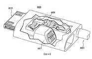
本發明之另一態樣係關於聲學路徑、埠及體積,其經建置經過小緊密耳機以便改良麥克風及/或揚聲器之聲學效能(對耳機之外形尺寸具有有限影響)。在一個實施例中,為控制經過耳芽之空氣之流動,聲學埠可整合於安置於其中的一或多個電子組件中及/或耳芽外殼中。在另一實施例中,經過各種外殼之埠中之至少一些大體上隱藏於視線外進而增強耳機的美學外觀。舉例而言,埠可定位於耳機之兩個界面外部表面之間的接縫內。在一個實例中,第一外部表面係由主外殼之管之開放末端提供,且第二外部表面係由安置於主外殼的管之開放末端內之末端部件提供。末端部件可(例如)包括連接器總成,進而將連接器與麥克風整合於相同表面區域中。Another aspect of the present invention relates to acoustic paths, ports, and volumes, which have been built through small tighteningClose earphones in order to improve the acoustic performance of the microphone and/or loudspeaker (has a limited impact on the size of the earphone) In one embodiment, in order to control the flow of air through the ear buds, the acoustic port may be integrated in one or more electronic components and/or the ear bud housing. In another embodiment, at least some of the ports passing through the various housings are substantially hidden from view to enhance the aesthetic appearance of the headset. For example, the port can be positioned in the seam between the outer surfaces of the two interfaces of the headset. In one example, the first outer surface is provided by the open end of the tube of the main housing, and the second outer surface is provided by the end member disposed within the open end of the tube of the main housing. The end piece may, for example, include a connector assembly, thereby integrating the connector and the microphone in the same surface area.
根據本發明之一個態樣,連接器總成可包括用於電力及資料之傳送的觸點。連接器可位於主外殼之相對於使用者介面按鈕之末端上。連接器可具有對稱組態,使得其可以一個以上界面定向(例如,90度對稱、180度對稱等)與互補連接器耦接。在一個實施例中,可包括切換電路以便容納此對稱。此電路可(例如)量測來自互補連接器之資料及/或電力線之極性,以確定其界面定向且基於所確定之定向而導引資料及/或電力線。在一些實施例中,連接器總成可至少部分由鐵磁材料組成,其可充當另一器件(例如,耳機充電器)中互補連接器上之一或多個磁體之吸引板。According to one aspect of the present invention, the connector assembly may include contacts for transmission of power and data. The connector can be located on the end of the main housing opposite to the user interface buttons. The connector can have a symmetrical configuration such that it can be coupled to a complementary connector with more than one interface orientation (eg, 90 degree symmetry, 180 degree symmetry, etc.). In one embodiment, a switching circuit may be included to accommodate this symmetry. This circuit can, for example, measure the data and/or the polarity of the power line from the complementary connector to determine its interface orientation and guide the data and/or the power line based on the determined orientation. In some embodiments, the connector assembly may be at least partially composed of a ferromagnetic material, which may act as an attraction plate for one or more magnets on a complementary connector in another device (eg, a headphone charger).
根據本發明之另一態樣,耳機可包括當不活動時隱藏不可見且當活動時可見之指示器。舉例而言,此可以可鑽入主外殼及/或耳芽部件之壁中之稱作微穿孔的微米大小之孔來完成。經由此等孔,主外殼及/或耳芽部件之內側上之光源可產生用於使用者的視覺指示器。可與此等微穿孔組合使用光擴散器使得指示器可以均勻分布光來照明。According to another aspect of the present invention, the headset may include an indicator that hides invisible when inactive and is visible when active. For example, this can be accomplished by micron-sized holes called micro-perforations that can be drilled into the walls of the main housing and/or ear bud components. Through these holes, the light source on the inner side of the main housing and/or the ear bud part can produce a visual indicator for the user. A light diffuser can be used in combination with these micro-perforations so that the indicator can evenly distribute light for illumination.
耳機可經由有線及/或無線連接與主機器件通信。有線連接可(例如)經由電纜/連接器配置產生。另一方面,無線連接可經由空中(無需實體連接)產生。有線及無線協定可廣泛變化。有線協定可(例如)基於通用串列匯流排(USB)介面、Firewire介面、習知串列介面、並列介面及/或類似物。無線協定可(例如)基於語音及/或資料之短程傳輸。無線協定可進一步用以在耳機與諸如蜂巢式電話之附近主機器件之間產生個人區域網路。可使用之無線協定之一些實例包括藍芽(Bluetooth)、Home RF、iEEE 8 02.11、IrDA、無線USB及類似物。通信電子器件可具體化為單晶片系統(SOC)。The headset can communicate with the host device via a wired and/or wireless connection. Wired connection can (for example)Generated via cable/connector configuration. On the other hand, wireless connections can be generated over the air (without physical connection). Wired and wireless protocols can vary widely. The wired protocol may, for example, be based on a universal serial bus (USB) interface, a Firewire interface, a conventional serial interface, a parallel interface, and/or the like. The wireless protocol may be based on short-range transmission of voice and/or data, for example. Wireless protocols can be further used to create personal area networks between headsets and nearby host devices such as cellular phones. Some examples of wireless protocols that can be used include Bluetooth, Home RF, iEEE 8 02.11, IrDA, wireless USB, and the like. The communication electronics can be embodied as a system-on-a-chip (SOC).
儘管可使用其他無線協定,但是根據本發明之一個態樣,耳機可包括基於藍芽無線協定之通信電子器件。通信電子器件可(例如)包括或對應於藍芽單晶片系統(SoC)。SoC可包括用於執行除無線通信之外的功能之電路。舉例而言,在一些實施例中,用於使用有線通用串列匯流排(USB)介面及習知串列介面通信之電路可整合於SoC中。Although other wireless protocols may be used, according to one aspect of the present invention, the headset may include communication electronic devices based on the Bluetooth wireless protocol. The communication electronics may, for example, include or correspond to a Bluetooth system on a chip (SoC). The SoC may include circuits for performing functions other than wireless communication. For example, in some embodiments, circuits for communication using a wired universal serial bus (USB) interface and a conventional serial interface can be integrated in the SoC.
對於增加之功能性,根據本發明之一個態樣,耳機可包括配電電路。此電路可(例如)視電池之電量或外部電源之可用性而定根據若干不同模式操作耳機。在一個模式中,配電電路可將電力供應至SoC之有限部分而同時對電池充電。電池充電過程可進一步藉由使用溫度偵測電路(例如,熱敏電阻)來監視電池溫度而改良。此過程可藉由僅當監視溫度處於或低於預定臨限值時對電池充電來延長電池壽命。在另一模式中,配電電路可使用電池對各種電子組件選擇性供電,而其他電子組件可由外部電源供電。For added functionality, according to one aspect of the invention, the headset may include a power distribution circuit. This circuit can, for example, operate the headset according to several different modes depending on the power of the battery or the availability of an external power source. In one mode, the power distribution circuit can supply power to a limited part of the SoC while simultaneously charging the battery. The battery charging process can be further improved by using a temperature detection circuit (for example, a thermistor) to monitor the battery temperature. This process can extend battery life by charging the battery only when the monitored temperature is at or below a predetermined threshold. In another mode, the power distribution circuit can use batteries to selectively power various electronic components, while other electronic components can be powered by an external power source.
下文關於圖1至圖68論述本發明之態樣及實施例。然而,熟習此項技術者將易於理解,本文中關於此等圖式給出之詳細描述用於解釋性目的,因為本發明經擴展超出此等有限實施例。The aspects and embodiments of the present invention are discussed below with respect to FIGS. 1 to 68. However, it will be easy to understand for those familiar with the technology. The detailed descriptions given in this article about these diagrams are for explanatory purposes.Because the present invention is extended beyond these limited embodiments.
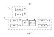
圖1為根據本發明之一個實施例之耳機10的簡化方塊圖。可以可被置於耳朵中之簡單聽筒之形式將耳機10組態為小緊密單元。耳機可包括主外殼11及自主外殼延伸之耳芽12。耳芽12可配合於耳朵中,進而緊靠使用者之臉部置放主外殼。此等部件中之每一者可圍繞並保護各種內部組件,且亦可將與操作耳機相關聯之各種外部組件支撐於其上。組件可為提供電子器件之特定功能之複數個電組件。舉例而言,組件通常可與產生、接收及/或傳輸與操作器件相關聯之資料相關聯。FIG. 1 is a simplified block diagram of a
耳機10包括用於控制耳機之功能之處理器20。在所說明之實施例中,處理器20可提供於耳芽12中。在其他實施例中,處理器20可位於耳機10中任何處。處理器20可經由電路板及/或電纜電耦接至耳機10之其他組件。處理器20可有助於與主機器件之無線通信。舉例而言,處理器20可產生用於無線傳輸之信號及處理所接收之無線信號。除無線通信之外,處理器20可協調耳機10之各種組件之操作。舉例而言,處理器20可控制電池之充電或顯示系統之操作。The
耳機10亦包括用於分配來自耳芽12之音訊資訊之揚聲器系統13。揚聲器系統13可包括在耳芽之末端處之音訊埠及安置於音訊埠之末端處之接收器(例如,揚聲器)。音訊埠可以護柵覆蓋。揚聲器系統13亦可包括耳芽內部及外部之各種埠。舉例而言,揚聲器系統13可包括耳芽內側之聲學路徑及穿過耳芽之表面的聲學路徑。The
耳機10亦包括用於對耳機提供輸入之一或多個輸入機構。輸入機構可置於主外殼及/或耳芽處。輸入機構可廣泛變化,且可包括,(例如):滑動開關、可按下按鈕、撥盤、輪、導航板、觸控板及/或類似物。出於簡易性之目的,耳機可僅包括單一輸入機構。此外,出於美觀原因,輸入機構可置於選擇位置。在其他實施例中,兩個或兩個以上輸入機構可駐留於耳機上。The
在一個實施例中,耳機10可包括位於主外殼11之一個末端處之單一按鈕14。將按鈕14置於末端節省主外殼11之側表面。此亦可藉由將耳芽12組態為按鈕(例如,耳芽可相對主外殼按下)來完成。耳芽12亦可經組態以傾斜、旋轉、彎曲及/或滑動,以便提供輸入同時節省主外殼11之側表面。In one embodiment, the
耳機10亦包括用於與主機器件通信之通信端子。通信端子可經組態用於有線或無線連接。在所說明之實施例中,通信端子為支援無線連接之天線15。天線15可位於主外殼或耳芽之內部。若主外殼或耳芽不由無線電穿透材料形成,則可需要提供無線電穿透窗。在所說明之實施例中,天線15位於耳機之一個末端處。將天線15及隨附無線電穿透窗置於末端處節省主外殼11之側表面。在一個實施例中,按鈕14及天線15整合於相同末端處。The
耳機10亦可包括用於將資料及/或電力傳送至耳機並自耳機傳送資料及/電力之一或多個連接器16。資料連接允許將資料傳輸至主機器件及自主機器件接收資料。另一方面,電力連接允許將電力傳遞至耳機。連接器可(例如)連接至基座(dock)或電纜中之相應連接器,以便連接至用於充電之電源及/或用於下載或上載的資料源。儘管連接器之位置可廣泛變化,但是在所說明之實施例中,連接器16位於末端中的一者處以便節省主外殼之側表面。The
在一些實施例中,連接器16及相應連接器可經成形使得兩個連接器可以兩個或兩個以上不同界面定向而配合。為補償此可能性,耳機10可包括耦接至連接器16之切換電路。此切換電路可確定連接器16如何與相應連接器耦接(例如,如何實體定向連接器)。切換電路可藉由量測(例如)來自互補連接器之資料及/或電力線之極性來確定此。切換電路可接著恰當地將資料及/或電力自連接器導引至耳機10中之其他電路。在一些實施例中,連接器16之至少一部分可為磁性的或磁性吸引的。舉例而言,連接器16可包括將其偏置至磁性連接器之鐵磁材料。此等磁性相互作用可輔助使用者將連接器16與相應連接器耦接,且有助於防止連接器去耦接。In some embodiments, the
耳機10亦包括用於捕獲由使用者提供之語音之麥克風17。麥克風通常位於主外殼內部。可將一或多個聲學埠組態於主外殼中以便提供自主外殼外側至麥克風之聲學路徑。聲學埠之位置可廣泛變化。在一個實施例中,聲學埠位於主外殼之一個末端處以便節省主外殼之側部。在一個實施例中,連接器總成及聲學埠整合於相同末端處。此外,可藉由埠之選擇性置放而將聲學埠組態為大體上不可見。舉例而言,埠可置於連接器總成與主外殼之間的接縫處。The
耳機10亦包括用於提供視覺反饋之顯示系統18。顯示系統可為包含能夠顯示圖形資訊之LCD或其他相關顯示器件之複合顯示系統,及/或其可為僅(例如)經由LED總成提供簡單視覺反饋的指示器總成。在一個實施例中,顯示系統僅包含沿主外殼之側壁提供視覺反饋之指示器總成。然而,為節省側壁,指示器總成可在不活動時隱藏。此可(例如)經由穿過主外殼之微穿孔來完成。微穿孔允許光穿過,但其太小而不可由使用者偵測。The
耳機10亦包括電池19。電池19可將電力提供至耳機10之組件。當外部電源連接至耳機10時,亦可提供充電電路以對電池19充電。在一個實施例中,耳芽可包含電力接收組件,其位於該耳芽外殼內,並經構形以自一充電裝置接收電力,並充電該可再充電的電池。The
耳機10亦可包括用於前述組件之支援電路。舉例而言,此可包括電路板、各種電組件、處理器及控制器。支援電路可置於主外殼及/或耳芽內側。在一個實施例中,支援電路可在兩個位置之間分裂或劃分以便得到更緊密器件,亦即各種電子器件根據需要而分布於體積中。為進一步節省空間,電子器件可為可堆疊的。在一個實施例中,電子器件可置於具有一或多個可撓性部分之電路板上,使得藉由摺疊或彎曲電路板產生堆疊。在一個實施例中,耳芽可包括電力傳輸電路,其經構形以與該電力接收組件電耦接,以提供電力至該耳芽。The
儘管耳芽12及主外殼11可形成為一體,但是在所說明之實施例中,主外殼及耳芽為可附接在一起之獨立外殼部件。任何合適之構件可用以將兩個部分附接在一起,包括(但不限於)螺桿、膠、環氧樹脂、夾片、托架及/或類似物。Although the
耳芽相對主外殼之位置可廣泛變化。舉例而言,耳芽可置於主外殼之任何外部表面處(例如,頂部、側部、前部或後部)。在一個實施例中,耳芽位於接近主外殼之末端中之一者處的平坦前側上。在一個實施例中,耳芽可經組態以相對主外殼移動使得其位置可加以調整。The position of the ear buds relative to the main shell can vary widely. For example, ear buds can be placed at any external surface of the main housing (e.g., top, side, front, or back). In one embodiment, the ear buds are located on the flat front side close to one of the ends of the main housing. In one embodiment, the ear buds can be configured to move relative to the main housing so that their position can be adjusted.
耳芽12及主外殼11中之每一者可經組態以圍繞其位於其周邊區域處之內部組件,以便覆蓋並保護內部組件。若需要其亦可經組態以在外部支援組件。耳芽12及主外殼11中之每一者有助於界定耳機之形狀及形式。亦即,其輪廓體現耳機之外向實體外觀。此等輪廓可為直線的、曲線的或兩者。在一個實施例中,將耳芽12形成為外向延伸之突出部件,而主外殼11形成為縱向延伸之部件。舉例而言,耳芽12可經由可為主外殼、耳芽或獨立零件一起之部分之頸部耦接至主外殼11。耳芽12及主外殼11之軸線可為橫向的,且更特定言之為垂直的。耳芽12及主外殼11之形狀可為廣泛變化的。在一個實施例中,耳芽12可經形成為反向圓形圓錐部件,且主外殼11可經組態具有藥丸狀橫截面。然而,應理解,此等並非限制且形式、形狀及定向可根據耳機之特定需要或設計改變。以實例說明,耳芽12及主外殼11可具有各種橫截面形狀,包括(例如):圓形、正方形、矩形、三角形、橢圓及/或類似形狀。另外,其形式可使得其不具有典型直軸線。Each of the
耳芽12及主外殼11可由一或多個部件形成。在一個實施例中,主外殼11可包括形成為一體之部件。藉由一體化,意謂部件為單一完整單元。藉由形成為一體,部件在結構上可比包括緊固在一起之兩部分之習知外殼更穩固。此外,不同於在兩部分之間具有接縫之習知外殼,部件具有大體上無縫外觀。此外,無縫外殼可防止污染且可比習知外殼更防水。主外殼可(例如)形成為管,其界定穿過其中位於第一開口與位於第一開口末端相對處之第二開口之間的空腔。為密封管之末端,主外殼可額外地包括一對端蓋。端蓋中之每一者可經組態以覆蓋開口末端中之一者,進而形成完全封閉的外殼系統。端蓋可由與管相似或不同材料形成。此外,端蓋可使用多種技術附接至管,包括(但不限於)緊固件、膠、夾片、托架及/或類似物。端蓋亦可經移動地附接,且經組態以承載耳機之操作組件。The
應理解,主外殼11之內部橫截面形狀可與主外殼之外部橫截面形狀相同或不同。舉例而言,可期望具有藥丸狀成形之外部及矩形成形之內部等。另外,儘管並非要求,主外殼11之前部及後部表面可為大體上平坦的。It should be understood that the internal cross-sectional shape of the main housing 11 may be the same as or different from the external cross-sectional shape of the main housing. For example, it may be desirable to have a pill-shaped outer portion, a rectangular-shaped inner portion, and the like. In addition, although not required, the front and rear surfaces of the main housing 11 may be substantially flat.
在一個實施例中,可經由擠壓或相關過程形成主外殼11。擠壓過程能夠在無接縫、裂痕、斷裂等之情形下產生整合管。如一般所熟知的,擠壓為藉由迫使熔融或熱材料經過成形之孔而產生連續工件之成形過程,亦即,擠壓過程產生具有特定橫截面形狀的長度。至少部分基於成形之孔來控制工件之橫截面形狀。隨著成形之工件離開孔,其經冷卻且隨後經切割至所要長度。擠壓過程為產生複雜輪廓並精確控制工件尺寸(其可為較小零件之必要性)之連續大量生產過程。此外,因為擠壓具有低加工成本,所以當與其他成形或製造過程相比時其為相對便宜的。In one embodiment, the main housing 11 may be formed through extrusion or a related process. The extrusion process can produce integrated pipes without seams, cracks, breaks, etc. As is generally known, squeezeCompression is a forming process that produces a continuous workpiece by forcing molten or hot material through a forming hole, that is, the extrusion process produces a length with a specific cross-sectional shape. The cross-sectional shape of the workpiece is controlled based at least in part on the formed hole. As the shaped workpiece leaves the hole, it is cooled and then cut to the desired length. The extrusion process is a continuous mass production process that generates complex contours and precisely controls the size of the workpiece (which can be a necessity for smaller parts). In addition, because extrusion has low processing costs, it is relatively inexpensive when compared to other forming or manufacturing processes.
主外殼11可由多種可擠壓材料或材料組合形成,包括(但不限於)金屬、金屬合金、塑膠、陶瓷及/或類似物。以實例說明,金屬可對應於鋁、鈦、鋼、銅等,塑膠材料可對應於聚碳酸酯、ABS、耐綸等,且陶瓷材料可對應於氧化鋁、氧化鋯等。氧化鋯可(例如)對應於二氧化鋯(zirconia oxide)。The main housing 11 may be formed of a variety of extrudable materials or material combinations, including (but not limited to) metals, metal alloys, plastics, ceramics, and/or the like. Taking examples to illustrate, metals can correspond to aluminum, titanium, steel, copper, etc., plastic materials can correspond to polycarbonate, ABS, nylon, etc., and ceramic materials can correspond to alumina, zirconia, etc. Zirconia may, for example, correspond to zirconia oxide.
圖2展示根據本發明之實施例之耳機連接器系統200。系統200可包括耳機210及耳機嚙合連接器220。在一些實施例中,耳機210可對應於圖1之耳機10。耳機210可包括安置於耳機之面部214內之任何數目的耳機連接器接觸區域(例如,見區域211、212及213)。面部214可與耳機嚙合連接器220配合,使得安置於耳機嚙合連接器中之相應數目之耳機嚙合接觸區域(例如,見區域221、222及223)與耳機連接器接觸區域電耦接。此外,耳機210可包括與耳機連接器接觸區域中之每一者電耦接之切換電路215。切換電路215可操作以確定耳機連接器接觸區域與耳機嚙合接觸區域之間的界面定向。舉例而言,切換電路215可確定耳機210與耳機嚙合連接器220配合之界面定向。切換電路215可藉由量測來自耳機嚙合連接器220之資料及/或電力線之極性來確定此。在已確定界面定向之後,切換電路215可基於所確定之定向而導引在耳機連接器接觸區域上接收之信號。應理解,可在連接器220中提供切換電路以提供類似於切換電路215之功能性。舉例而言,連接器220中之切換電路可確定耳機210之界面定向,並基於所確定的定向將電信號導引至接觸區域。Figure 2 shows an
在一些實施例中,耳機210之至少一部分及/或耳機嚙合連接器220(例如,外殼224之部分或全部)可為磁性吸引的。此外,耳機嚙合接觸區域(例如,見區域221、222及223)可經偏置以自連接器220之外殼224突出。在此等實施例中,耳機210可經磁性吸引至耳機嚙合連接器220,使得磁力可使耳機嚙合接觸區域(例如,見區域221、222及223)相抵耳機連接器接觸區域(例如,見區域211、212及213)擠壓。In some embodiments, at least a part of the
圖3展示根據本發明之實施例之電子器件300。在一些實施例中,器件300可為電子耳機(例如,見圖1之耳機10),但應理解,器件300不限於電子耳機。器件300可包括外殼310及連接器總成320。連接器總成320之至少一部分可安置於外殼310中。連接器總成320可包括埠322、麥克風324及將麥克風流體耦接至埠之通道326。連接器總成320亦可包括用於與另一器件電耦接之一或多個觸點(例如,見觸點321、323、325及327)。可在一位置提供埠322使得連接器總成320之觸點與埠位於相同外部表面上或位於附近。在一些實施例中,埠322可位於兩個觸點(例如,見觸點323及325)之間。FIG. 3 shows an
圖4展示根據本發明之另一實施例之電子器件400。類似於器件300,器件400在一些實施例中可為電子耳機(例如,見圖1之耳機10),但應理解,器件400不限於電子耳機。器件400可包括外殼410及接合連接器及麥克風總成420。麥克風430、罩440及連接器板450可提供於接合連接器及麥克風總成420中。麥克風430可包括一或多個側表面及具有麥克風埠432之頂部表面。麥克風罩440可安裝至麥克風,使得罩與頂部表面之至少一部分及側表面形成密封。此密封可圍繞麥克風埠432。麥克風罩440可進一步包括用於密封至連接器板450之部分及用於將麥克風埠432流體連接至連接器埠452之孔。連接器板450可包括用於與另一器件電耦接之一或多個觸點(例如,見觸點451、453、455及457)。可在一位置提供連接器埠452,使得埠與連接器總成420之觸點位於相同外部表面內或位於觸點附近。在一些實施例中,埠452可位於兩個觸點(例如,見觸點453及455)之間。FIG. 4 shows an
圖5展示根據本發明之實施例之耳機500。耳機500可對應於電子耳機(例如,見圖1之耳機10)且可包括主外殼510及耳芽520。舉例而言,主外殼510可對應於主外殼11,且耳芽520可對應於耳芽12。耳芽可撓性電路板522可提供於耳芽520中。接收器524及處理電路526可安裝於耳芽可撓性電路板522上。耳芽可撓性電路板522可為可撓性的,使得其可摺疊於其自身上或彎曲。此可撓性可允許耳芽可撓性電路板522配合於較小或較不常見成形之耳芽中。Figure 5 shows a
主外殼510可固定至耳芽520。主外殼510可包括主外殼可撓性電路板512及麥克風514。類似於耳芽可撓性電路板522,主外殼可撓性電路板512可為可撓性的,使得其可摺疊於其自身上或彎曲。此可撓性可允許主外殼電路板512彎曲圍繞主外殼中之其他組件(例如,電路、天線或電池),以便節省主外殼內側之內部空間。舉例而言,節省內部空間可產生較多空間以容納較大電池。在另一實例中,節省內部空間可產生較小主外殼。耳芽可撓性電路板522及麥克風514可電耦接至主外殼可撓性電路板512。在一些實施例中,諸如圖5中所展示之實施例,耳芽可撓性電路板522可延伸至主外殼510中使得其可與主外殼可撓性電路板512耦接。在其他實施例中,主外殼可撓性電路板512可延伸至耳芽520中使得其可與耳芽可撓性電路板522耦接。應理解,儘管將主外殼可撓性電路板512及耳芽可撓性電路板522描述為可撓性的,但是一個或兩個電路板可包括可撓性部分及剛性部分。舉例而言,每一電路板可包括一或多個剛性部分,電組件(例如,接收器524、處理電路526或麥克風514)可易於且穩定地安裝於該一或多個剛性部分上。The
圖6A展示根據本發明之實施例之耳機器件600。耳機器件600可包括耳芽外殼610、螺紋頸620及主外殼630。耳機器件600可對應於圖1之耳機10,使得(例如)耳芽外殼610對應於耳芽12且主外殼630對應於主外殼11。耳芽外殼610可包括耳芽通孔612及頸嚙合表面614。螺紋頸620可包括可與耳芽外殼之頸嚙合表面614配合之第一頸表面622。第一頸表面622及頸嚙合表面614可包括一或多個特徵(例如,突起、突出、槽或凹口),使得其可僅以某一定向(相對於彼此)耦接。FIG. 6A shows an
主外殼630可包括主外殼通孔632及頸嚙合表面634。螺紋頸620可進一步包括可與主外殼之頸嚙合表面配合之第二頸表面624。第二頸表面624及頸嚙合表面634可包括一或多個特徵(例如,突起、突出、槽或凹口),使得其可僅以某一定向(相對於彼此)耦接。The
圖6B展示用於與根據本發明之耳機器件600一起使用之螺桿690。螺桿690可用作耳芽螺桿及主外殼螺桿。螺桿690可包括行進穿過螺桿之中心之中空通道692。螺桿690亦可包括特徵694(例如,凹口),使得工具可與特徵建立界面並旋轉螺桿。作為耳芽螺桿,螺桿690可插入耳芽通孔612中且拉緊,使得其將頸嚙合表面614緊固至第一頸表面622。作為主外殼螺桿,螺桿690可插入主外殼通孔632中且拉緊,使得其將頸嚙合表面634緊固至第二頸表面624。Figure 6B shows a
圖7展示根據本發明之實施例之顯示系統700。顯示系統700可(例如)對應於圖1之顯示系統18。系統700可包括外殼710、光源720、擴散器730及控制電路740。外殼710可具有安置於其中之信號指示器區域712。信號指示器區域712可(例如)為用於透射光之一或多個孔(例如,微穿孔)。信號指示器區域712可經組態以輸出具有某一形狀或形式之信號。外殼710亦可包括內部壁714。擴散器730可位於光源720與內部壁714之間。控制電路740可與光源720電耦接以控制光源720何時發射光。FIG. 7 shows a
擴散器730可操作以擴散來自光源720之光,使得離開擴散器之所有光具有相等強度或亮度。舉例而言,擴散器730可操作以藉由來自光源720之光均勻照明信號指示器區域712。擴散器730可由引發光擴散之不同微粒之混合物構成。舉例而言,擴散器730可包括主要透明之微粒,其具有遍及分布之半透明微粒。半透明微粒可引發光自其原始路線偏轉,使得光遍及擴散器分布。因此,自擴散器之任何部分離開之光將具有大體上均勻亮度。The
圖8展示根據本發明之實施例之配電系統800。配電系統800可用於電子器件(例如,見圖1之耳機10)中,且可包括開關810、匯流排820、第一功率調節電路822、核心處理電路824、電池830、第二功率調節電路832、RF處理電路834及控制電路840。核心處理電路824可包括用於處理電子器件之低位準、核心功能之電路,且RF處理電路834可包括用於處理電子器件的RF通信之電路。為對核心處理電路824及RF處理電路834供電,配電系統800可包括匯流排820及作為潛在電源之電池830。Figure 8 shows a
匯流排820可經耦接以接收來自系統外部之電源之電力。舉例而言,匯流排820可耦接至連接器使得匯流排可經由連接器接收電力。第一功率調節電路822可電耦接至匯流排820及核心處理電路824。第一功率調節電路822可操作以(例如)將來自匯流排820之電力轉換為適合用於核心處理電路824之狀態(例如,藉由改變電壓或調節電流)。The
電池830可為儲存化學能並使其以電形式可用之器件。電池830可為可再充電的。第二功率調節電路832可電耦接至電池830及RF處理電路834。第二功率調節電路832可操作以(例如)將來自電池830之電力轉換為適合用於核心處理電路824之狀態(例如,藉由改變電壓或調節電流)。The
開關810可電耦接至核心處理電路824及RF處理電路834。開關810可由匯流排820上之外部電源之存在控制。舉例而言,當匯流排820之電壓低於預定臨限值時開關810可為活動的。當開關810為活動時,第一功率調節電路822、核心處理電路824、RF處理電路834及第二功率調節電路832可電耦接使得核心處理電路及RF處理電路可共用電力。The
控制電路840可電耦接至匯流排820、第一功率調節電路822、核心處理電路824及第二功率調節電路832。控制電路840可能夠基於匯流排820、核心處理電路824及/或電子器件中之任何其他信號選擇性活化第一功率調節電路822及第二功率調節電路832。The
圖9展示根據本發明之實施例之無線耳機900。耳機900可為用於通信之電子耳機(例如,見圖1之耳機10)。耳機900可包括具有第一功率消耗部分912及第二功率消耗部分914之處理器電路910。第一功率消耗部分912可(例如)包括電子器件之核心電路(例如,啟動電路),而第二功率消耗部分914可包括器件之輔助電路(例如,RF通信之電路)。耳機900可進一步包括配電電路920。配電電路920可獨立於第二功率消耗部分914是否被供電而選擇性對第一功率消耗部分912供電。在一些實施例中,配電電路920可基於耳機900之一或多個所監視狀態選擇性對第一功率消耗部分912及第二功率消耗部分914之任何組合供電。舉例而言,配電電路920可監視外部電源是否存在及/或內部電池之電量以便確定啟動哪些功率消耗部分。Figure 9 shows a
圖10A及圖10B展示根據本發明之實施例之說明性耳機的透視圖。耳機1000可對應於圖1之耳機10。舉例而言,主外殼1010可對應於主外殼11且耳芽1020可對應於耳芽12。10A and 10B show perspective views of illustrative earphones according to an embodiment of the invention. The
耳機1000可包括封閉耳機之電子器件及其他元件之外殼。外殼可併入使用任何合適之過程(例如,黏著劑、螺桿或壓入配合)裝配之若干零件。在圖10A及圖10B之實例中,耳機1000可包括耳芽1020、頸1030、主外殼1010、天線蓋1011及連接器1040。耳芽1020可包括用於允許空氣出入耳芽1020之穿孔(例如,聲學埠)1021及1022。前埠1021可允許來自位於耳芽1020中之接收器之聲波達到使用者的耳朵及/或外側環境。側埠1022(例如:聲學排出口)可提供用於聲壓排出至外側環境之路徑。耳芽1020可藉由頸1030附接至主外殼1010。The
天線蓋1011附接至主外殼1010之一個末端。天線蓋1011可具有經安置至少部分穿過其中之按鈕1012。使用者可與按鈕1012建立介面以控制耳機。主外殼1010可包括可對應於圖7之顯示系統700或圖1之顯示系統18之顯示器1013。在一些實施例中,顯示器1013可包括微穿孔,諸如下文結合圖48及圖49較詳細論述之微穿孔。位於主外殼1010之連接器末端處之連接器1040包括用於使外殼1010內側的麥克風能夠接收聲學信號(例如,使用者之語音)之至少一埠(圖10A中未圖示),及用於自外部電源接收電力、資料或兩者之至少一觸點1042。舉例而言,連接器1040可對應於圖2之接觸區域211、212及213。The
耳芽1020、頸1030、主外殼1010、天線蓋1011及連接器1040可由任何合適之材料建構,包括(例如)金屬、塑膠、聚矽氧、橡膠、發泡體或其組合。舉例而言,耳芽1020可由藉由聚矽氧密封圍繞之塑膠元件形成,且主外殼1010可由鋁形成。耳芽1020、頸1030、主外殼1010、天線蓋1011及連接器1040可使用任何合適之過程(例如,模製、澆鑄或擠壓)製造。在一些實施例中,耳芽1020、頸1030、主外殼1010、天線蓋1011及連接器1040可經後處理以在本體之內部或外部表面上提供紋理及其他特徵。舉例而言,珠粒噴擊及陽極化過程可用以將所要表面紋理施加至主外殼1010。The
圖11為根據本發明之實施例之耳機1100的分解圖。舉例而言,耳機1100可對應於圖1之耳機10或圖10A及圖10B之耳機1000。在本發明之一個實施例中,耳芽外殼1120可含有耳芽電路板1122。耳芽電路板1122可(例如)對應於圖5之耳芽電路板522。耳芽電路板1122可為可撓性電路板,以下組件中之一或多者電性及/或機械安裝於可撓性電路板上:處理器1123(其可用以控制耳機1100之功能)、接收器1124及其他電路及組件。耳芽電路板1122之可撓性性質可使其能夠摺疊於其自身上,提供可封裝於耳芽外殼1120中之電路層,藉此佔據耳芽外殼1120內可原本為空的及未使用的空間。耳芽電路板1122之可撓性部分可替代對連接不同電路板之獨立導線的需要,其可引發大小之實質增加,因為(例如)每一導線可能涉及一對連接器。另外,電路板1122之可撓性性質可有利地減少由電路板1122需要之面積或佔據面積。亦即,與具有相似電路及組件安置於其上但以展開布局之另一電路板相比,電路板1122可佔據更少面積。另外,電路板1122進一步可藉由在耳芽外殼1120內併入通常位於耳機內其他處之電子器件及其他組件來減少耳機1100之其他組件(諸如主外殼1110及天線蓋1111)的佔據面積或大小要求。舉例而言,在下文中結合圖18至圖27B較詳細地論述耳芽外殼1120及含於其中之電路及組件。FIG. 11 is an exploded view of a
耳芽外殼1120可由頸1130耦接至主外殼1110。耳芽外殼1120、主外殼1110及頸1130可分別對應於圖6A之耳芽外殼610、主外殼630及頸620。頸1130可藉由雙螺紋螺桿插入物建構以收納螺桿部件1131(與耳芽外殼1120相關聯)及螺桿部件1132(與主外殼1110相關聯)。頸1130可藉由可減少耳芽外殼1120及主外殼1110彼此獨立旋轉之可能性的方式來連接耳芽外殼1120及主外殼1110。亦即,當耳機1100處於使用中,且使用者藉由(例如)拉下主外殼1110調整其位置時,耳芽外殼1120可結合主外殼1110旋轉。然而,在一些實施例中,拉下主外殼1110可引發外殼相對於耳芽外殼1120旋轉以便觸發開關並表示使用者輸入。舉例而言,下文可結合圖28至圖30找到耳機頸及其總成之較詳細論述。The
除耳芽電路板1122之外,耳機1100亦可包括主外殼電路板1115,額外電子組件1113可電性及/或機械安裝於主外殼電路板1115上。主外殼電路板1115可(例如)對應於圖5之主外殼電路512。主外殼電路板1115可藉由一或多個導線、電纜、可撓性電路板及類似物與耳芽電路板電耦接。耳芽電路板1122及主外殼電路板1115中之電子組件之配置可有利地減少耳機1100的大小。舉例而言,下文中將結合圖18至圖20C較詳細地論述耳機1100中之電子組件之配置。In addition to the
使用者可使用可與主外殼電路板1115電耦接之按鈕1112來控制耳機1100之功能。按鈕1112可自天線蓋1111延伸使得其呈現為易於由使用者啟動之離散使用者介面。按鈕1112可經組態以任何合適之方式移動,包括(例如)相對於主外殼1110彎曲、平移出入天線蓋1111、圍繞穿過連接器板1141及按鈕1112之軸線旋轉,或其任何組合。The user can use the
在一個實施例中,按鈕1112可包括開關,諸如薄膜按鍵開關(dome switch),其可當使用者按下按鈕1112時啟動。按鈕1112可具有按鈕導引結構。按鈕導引結構可具有一或多個導引通道以有助於按鈕關於耳機1100之其餘部分之使用者致動。在本發明之一個實施例中,導引通道可以經過按鈕導引結構之孔的形式提供。開關致動部件可具有由導引通道支撐及導引之桿。當由使用者按下時,開關致動部件沿導引通道朝向開關移動。升高之結構(例如,肋狀物)可用以確保開關致動部件在導引通道內平滑地往復運動。In one embodiment, the
按鈕1112及天線蓋1111可由諸如塑膠之介電材料建構。天線1118可藉由將天線諧振元件安裝於天線蓋1111內(例如,沿天線蓋1111之內表面)或安裝於按鈕導引結構之一部分上而形成。由介電材料建構按鈕1112及天線蓋1111可減少或消除可干擾天線1118之恰當操作之潛在信號干擾。另外,介電材料建構之按鈕1112可允許耳機1100中之天線諧振元件與導電結構(例如,主外殼電路板1115)之間的較小間隙。The
天線1118可與主外殼電路板1115電耦接,使得其可發送並接收無線(例如,無線電)信號。天線1118可包括用於在耳機1100與電子器件(例如,蜂巢式電話或個人媒體器件)之間通信的任何合適之天線諧振元件。天線諧振元件可由含有導體條帶之撓性電路形成。撓性電路可使用(例如)黏著劑附接至按鈕導引結構。舉例而言,撓性電路可含有與按鈕導引結構上之相應定位突起配合之定位孔。突起中之一或多者可經熱熔至撓性電路。The
可在(例如)題為"Antenna and Button Assembly for Wireless Devices"的美國專利申請案第11/651,094號中找到關於類似於天線1118及按鈕1112之天線及按鈕系統之操作及設計之細節,該案併入本文中。Details on the operation and design of an antenna and button system similar to
附件1117可併入天線蓋1111中以便將天線蓋安裝至耳機1100。附件1117可(例如)緊固至主外殼1110或將在下文較詳細論述之一或多個托架1116。The
電池組1119可位於主外殼1110內。電池組1119可含有一或多個合適之電池,包括(例如)鋰離子、鋰離子聚合物(Li-Poly)、鎳金屬氫化物或任何其他類型之電池。電池組1119可與電路板1115電耦接用於對耳機1100中之電子組件供電。另外,通常封裝於標準電池組內之電路(例如,充電或熔斷器保護電路)可移動至主外殼電路板1115。有利地,電路分布於耳芽外殼1120中及電路板1115之布局可允許電池組1119佔據主外殼1110之內部空間的實質部分。此可在未增加主外殼1110及耳機1100之大小之情形下增加耳機1100的能量儲存容量(例如,允許耳機1100在充電之間操作持續較長時間週期)。The
耳機1100可包括用於使耳機1100能夠電連接至其他器件之連接器1140。開口或埠可包括於連接器1140中,使得聲學信號(例如,來自使用者之語音)可到達麥克風罩1144內側之麥克風。舉例而言,連接器1140可(例如)對應於圖3之總成320或圖4之總成420。麥克風可藉由任何合適之方式與電路板1115電耦接。麥克風罩1144可置於主外殼1110之距耳芽外殼1120最遠之末端內側。此末端在本文中可稱為麥克風或耳機1100之連接器末端,且亦為當使用時耳機1100之較接近使用者的嘴部之部分。下文結合隨附圖50A至圖54之描述較詳細地論述麥克風罩1144相對於連接器1140及隨附零件之配置。The
連接器1140可包括觸點1142及隨附套管1143可駐留於其中之連接器板1141。因而,觸點1142可有助於耳機1100與另一器件之電耦接。隨附套管1143可由非傳導材料(例如,聚合材料)製造。套管1143可圍繞觸點1142以防止觸點與連接器板1141電耦接。觸點1142及套管1143可與連接器板1141之表面大體上平齊,使得觸點、套管及板之組合產生用於與其他連接器配合的大體扁平表面。連接器板1141可由鐵磁材料製成,使得其經偏置至磁性連接器(例如:第一磁性耦接機構),例如結合圖62A至圖67B所論述之磁性連接器。下文將結合圖55A至圖67B之論述較詳細地描述連接器板1141、觸點1142、套管1143及互補磁性連接器(例如:第二磁性耦接機構)之設計。The
耳機1100可包括一或多個托架1116以將連接器1140與天線蓋1111之附件1117耦接。托架1116可防止連接器板1141及天線蓋1111彼此軸向移動離開或與主外殼1110分離。或者,連接器板1141及天線蓋1111可耦接至緊固至主外殼1110之內表面之一或多個托架。The
出於設計選擇,連接器板1141之周邊表面與主外殼1110之內表面之間可包括接縫。亦即,除用於在麥克風與外側環境之間提供聲學路徑之預定埠之外,可存在間隙。此等間隙可有利地使麥克風在預定聲學路徑被阻斷(例如,由諸如汙物之外來物件)之情形下能夠接收聲學信號。在其他實施例中,可塗覆黏著劑以在連接器板1141與主外殼1110之間提供實質上氣密密封。在又一實施例中,密封墊可用以提供密封。For design choice, a seam may be included between the peripheral surface of the
圖12展示根據本發明之另一實施例之耳機1200的圖。耳機1200可類似於耳機1100,但兩者之間具有一些實質差異。舉例而言,耳機1200可使用不同附接技術來將連接器1240耦接至主外殼1210。連接器1240可包括可用以與主外殼1210之內部表面上之特徵(例如,壁1212)耦接的突出1242。此方法可有利於使用耳機1100中之托架1116。舉例而言,突出1242可附接至主外殼1210之近端,其可提供具有比(例如)使用托架來附接至主外殼之另一末端上的結構(例如,天線蓋)之方法更高結構整合性之連接器1240。耳機1200亦可包括可結合如結合圖48及圖49所論述之視覺指示器系統使用之光擴散器1244。另外,耳機1200可包括在一些實施例中可包覆按鈕導引1217之天線1218。FIG. 12 shows a diagram of a
藍芽協定之基本原理在此項技術中已知,且在下文簡要論述。關於較詳細之論述,請參見Bluetooth Specification Version 2.0+EDR,第0卷,2004年11月4日,其整體以引用之方式併入本文中。藍芽無線技術係基於用於允許智能器件經由無線、低功率、短程通信彼此通信之國際、公開標準。此技術允許任何種類之電子裝備(自電腦及手機至鍵盤及頭戴耳機)在無導線或來自使用者之任何直接行動的情形下進行其自身之連接。藍芽被併入包括膝上型電腦、PDA、手機及印表機之眾多商業產品中,且可能用於未來產品中。The basic principles of the Bluetooth protocol are known in this technology and are briefly discussed below. For a more detailed discussion, please refer to Bluetooth Specification Version 2.0+EDR,
藍芽可稱為在2.4GHz免照頻帶中操作之跳頻展頻(FHSS)無線電系統。藍芽傳輸基於發射器及接收器兩者皆已知之序列改變頻率。根據一個已知標準,藍芽傳輸使用介於2.404GHz至2.480GHz之間的79種不同頻率。藍芽之低功率傳輸允許約10米或大約30至40呎之典型範圍。此範圍可取決於由用於藍芽傳輸之器件使用之功率量而在介於約1米至100米之間變化。Bluetooth can be referred to as a Frequency Hopping Spread Spectrum (FHSS) radio system operating in the 2.4GHz unlicensed frequency band. Bluetooth transmission is based on a sequence that is known to both the transmitter and the receiver to change the frequency. According to a known standard, Bluetooth transmission uses 79 different frequencies between 2.404GHz and 2.480GHz. Bluetooth's low power transmission allows a typical range of about 10 meters or about 30 to 40 feet. This range can vary from about 1 meter to 100 meters depending on the amount of power used by the device used for Bluetooth transmission.Between changes.
藍芽器件彼此連接以形成稱作微網(piconet)之網路。微網包括經同步至共同時脈信號及跳頻序列之兩個或兩個以上器件。因此,對於連接至給定微網之任何器件,彼器件可需要具有相同時脈信號及跳頻序列。經同步之時脈及跳頻序列可使用微網上之器件中的一者之時脈信號導出。此器件常常稱為"主控"器件,而微網上所有其他器件稱為"受控"器件。每一微網可包括一個主控器件及多達七個或七個以上受控器件。此外,藍芽器件可屬於一個以上微網。術語"散網(scatternet)"用以定義由多個、重疊微網組成之藍芽網路。在一個藍芽器件位於兩個或兩個以上微網上之狀況下,所有器件位於單一散網上。來自微網中之一者之器件可藉由使用共用器件以延遲信號來與來自另一微網的器件通信。Bluetooth devices are connected to each other to form a network called piconet. The microgrid includes two or more devices synchronized to a common clock signal and frequency hopping sequence. Therefore, for any device connected to a given microgrid, that device may need to have the same clock signal and frequency hopping sequence. The synchronized clock and frequency hopping sequence can be derived using the clock signal of one of the devices on the micronet. This device is often called a "master" device, while all other devices on the micronet are called "controlled" devices. Each microgrid can include a master control device and up to seven or more controlled devices. In addition, Bluetooth devices can belong to more than one piconet. The term "scatternet" is used to define a Bluetooth network consisting of multiple, overlapping microgrids. In a situation where one Bluetooth device is located on two or more micronets, all devices are located on a single discrete network. A device from one of the microgrids can communicate with a device from another microgrid by using a common device to delay the signal.
當兩個藍芽器件初始連接時,其彼此首先共用某總體資訊(例如,器件名稱、器件類型)。為增強連接,器件可藉由使用秘密通行鑰建立可信賴關係。此通行鑰通常由使用者提供或儲存於器件中之記憶體上。根據已知藍芽標準,建立此可信賴關係之過程稱為配對。一旦兩個器件經配對,其通常共用資訊並接受來自彼此之指令。When two Bluetooth devices are initially connected, they first share certain general information (for example, device name, device type) with each other. To enhance the connection, the device can establish a trustworthy relationship by using a secret pass key. This pass key is usually provided by the user or stored in the memory in the device. According to known Bluetooth standards, the process of establishing this trustworthy relationship is called pairing. Once the two devices are paired, they usually share information and accept commands from each other.
藍芽器件可以大致2.1Mbit/s(每秒百萬位元)之最大資料通量操作,但是應理解,此等限制隨著技術進步而改變,且本發明之實施例可以其他速率操作。此最大通量在微網上之所有器件之間共用,意謂若一個以上受控器件與主控器通信,則所有通信之總和小於最大資料通量。The Bluetooth device can operate at a maximum data throughput of approximately 2.1 Mbit/s (million bits per second), but it should be understood that these limitations change as technology advances, and embodiments of the present invention can operate at other rates. This maximum flux is shared among all devices on the micronet, which means that if more than one controlled device communicates with the master, the sum of all communications is less than the maximum data flux.
藍芽標準包括公開軟體構架。共用構架稱為藍芽協定堆疊且包括不同軟體應用程式來實施藍芽通信。圖13為根據本發明之實施例之例示性藍芽協定堆疊1300之簡化示意圖。低階軟體包括於下部堆疊1302中。此區段包括用以產生/接收無線電信號,校正傳輸誤差及加密/解密傳輸之程式碼。主機控制器介面(HCI)1304為低階藍芽功能與應用程式之間的標準化介面。HCI層表示由專用藍芽處理器處理之下部堆疊1302功能與由特定應用處理器處理之其餘功能之間的劃分。The Bluetooth standard includes a public software architecture. The shared framework is called the Bluetooth protocol stack and includes different software applications to implement Bluetooth communication. FIG. 13 is a simplified schematic diagram of an exemplary
延伸同步連接導向(eSCO)1306層用以在下部堆疊1302與高階應用程式之間實施專用通信通道(通常用於語音資料)。邏輯連接控制及適應協定(L2CAP)1308層結合並重封裝由多個較高階應用程式發射及接收之資料。L2CAP 1308層將所有此等不同通信整合為可與下部堆疊1302建立介面之一個資料流。RFCOMM 1310層仿效由串列連接使用之協定。此允許軟體設計者易於將藍芽整合於先前使用串列連接之現存應用程式中。服務發現協定(SDP)1312層由器件使用以提供關於每一器件提供何等服務(或功能)及其他器件可如何經由藍芽存取彼等服務之資訊。The extended synchronous connection orientation (eSCO) 1306 layer is used to implement a dedicated communication channel (usually used for voice data) between the
框架1314層允許器件將其自身識別為具有預定功能集合之器件之通用群組的成員。舉例而言,符合耳機框架之器件可支援關於音訊通信之預定方法。應用程式層1316含有實施由所有其他層產生之有用工具之程式。藉由寫入用於應用程式層1316之不同程式,軟體開發者可在無需重寫入控制基本通信任務之程式碼的情形下專注於藍芽功能性之新用途。The
圖14展示根據本發明之實施例之耳機的例示性電子系統1400之簡化方塊圖。1400之系統可實施於(例如)圖1之耳機10或圖10A及圖10B的耳機1000中。系統1400可包括處理器電路1410、介面電路1420、配電電路1430、切換電路1440及4插腳對稱磁性連接器1450。FIG. 14 shows a simplified block diagram of an exemplary
處理器電路1410可包括處理器1411及結合處理器1411操作之輔助電路。處理器1411可協調系統1400中之所有操作,包括(例如)藍芽傳輸、電池充電及聲學信號之處理(例如,編碼及解碼)。處理器1411可驅動接收器1412以提供可由使用者聽到之聲學信號。重設電路1413可偵測系統1400何時連接至另一器件並隨後命令處理器1411重設。功率場效應電晶體(FET)1414可與處理器1411內側之電源電路使用,且將結合圖15之論述在下文中較詳細論述。天線1415可用以將無線信號發送至另一器件(例如,電話或攜帶型媒體器件)及自另一器件接收無線信號。通用異步收發器(Universal Asynchronous Receiver and Transmitter,UART)多工器1416可與處理器1411電耦接,且將資料信號導引至處理器1411之不同部分。此導引可減少未使用資料線中之不良效應,諸如電感。The
介面電路1420可包括麥克風隔離低壓降調節器(Low Dropout Regulator,LDO)1421、微機電(MEMs)麥克風1422、LED驅動器1424及開關1423。麥克風隔離LDO 1421可與MEMs麥克風1422電耦接。麥克風隔離技術及MEMs麥克風已為吾人所熟知,且熟習此項技術者將理解,此等元件可在未脫離本發明之精神之情形下由其他等效麥克風組態替代。LED驅動器1424可經組態以基於處理器1411之一或多個輸出驅動LED顯示單元。關於類似於LED驅動器1424之電路之設計及功能之細節可在題為"Systems and Methods for Compact Multi-State Switch Networks"的美國專利申請案第60/878,852號中找到,該案併入本文中。開關1423可呈圖10B之按鈕1012之電行為。使用者可與此開關建立介面以將命令輸入至耳機。舉例而言,使用者可按下開關1423以起始電話呼叫、終止呼叫或兩者。在一個實施例中,開關1423可為具有將其偏置至開路位置之彈簧之單極、單投開關。The
配電電路1430可包括過壓保護及保險絲1431、電池保護電路1432及熱敏電阻1433。過壓保護及保險絲1431可在不安全之電壓量被施加至一或多個輸入之情形下保護系統1400。保護電路中之保險絲可為若偵測到過流狀態則斷開耳機之輸入之過流保護器件。電池保護電路1432可包括用以防止電池(例如,鋰聚電池)之可導致危險過熱情形之故障的電路。與具有整合入電池組之此電路之習知耳機對比,電池保護電路1432可與電池組分離且位於根據本發明的耳機內之其他處。熱敏電阻1433可位於接近電池(例如,見圖11之電池組1119)處,且可基於電池之溫度改變其電阻。處理器1411之一或多個輸入可與熱敏電阻1433電耦接以監視電池之溫度。處理器1411可經程式化以視所偵測之電池溫度而不同地對電池充電。舉例而言,處理器1411在所監視之電池溫度低時可以比溫度高時更快之速率對電池充電。藉由以此方式調節充電,可在未損傷電池之情形下減少完成對電池充電所需之時間。The
對稱磁性連接器1450可允許系統1400連接至用於通信資料或傳輸電力之其他器件及系統。舉例而言,連接器1450呈圖1之連接器16之電行為。The symmetrical
切換電路1440可使連接器1450能夠與許多不同類型之器件並以許多介面定向連接及通信。切換電路1440可(例如)對應於圖2之切換電路215。切換電路1440可包括電力極性切換電路1441及資料極性切換電路1442。兩個電路可(例如)確定所使用之通信介面之類型,且將相應資料及/或電力線導引至用於所偵測介面之正確路徑(例如,內部電迹線)。舉例而言,兩個電路亦可確定與另一器件之連接之介面定向,且將相應資料及/或電力線導引至用於所偵測定向之正確路徑(例如,內部電迹線)。類似於切換電路1441及1442之例示性電路之設計及功能的詳細描述可在題為"Systems and Methods for Determining the Configuration of Electronic Connections"之美國專利申請案第11/650,130號中找到,該案併入本文中。The
圖15展示可用作根據本發明之實施例之耳機的核心處理器或應用程式處理器之處理器1500。處理器1500可(例如)對應於圖1之處理器20。處理器1500亦可稱作單晶片系統(SoC),因為其可為具有不同範圍之功能之單一積體電路。處理器1500可為具有充分支援藍芽V2.0+EDR規格之整合快閃記憶體之CSR BC04音訊處理器。振盪器1510及時脈產生電路1511可結合計時晶體使用以建立處理器1500可用以協調其活動之時序信號(或時脈)。RF電路1520可用以輸入及輸出用於無線通信之RF信號。基頻電路1530可協調通信使得其符合通信協定(例如,藍芽協定)。快閃記憶體1531可儲存(例如)用於處理器1500之軟體及組態資訊。隨機存取記憶體(RAM)1532可臨時儲存用於基頻電路1530及RISC微處理器1533之資料。RISC微處理器1533可經程式化以執行各種功能,諸如監視熱敏電阻(例如,見圖14之熱敏電阻1433)及協調如先前所述之電池充電。FIG. 15 shows a
全速USB控制器1540及UART電路1541可有助於有線通信介面,使得處理器1500可經由實體界面(例如,圖10A之連接器觸點1042)與另一器件共用資料。在一個實施例中,處理器1500可支援全速USB及簡化RS-232串列介面。簡化RS-232介面可包括(例如)三個線:發射資料、接收資料及接地。為在有限數目之資料線上容納一個以上介面,USB控制器1540及UART電路1541可耦接至開關(例如,圖14之UART多工器1416)。此開關可將資料線導引至處理器1500內之電路,其對應於所使用之通信介面。用於在有限數目之資料線上使用一個以上通信介面之相似系統及方法的較詳細論述可在題為"Systems and Methods for Determining the Configuration of Electronic Connections"之美國專利申請案第11/650,130號中找到,該案併入本文中。在未背離本發明之精神之情形下,處理器1500亦可支援除上文所論述之介面之外的其他介面。舉例而言,處理器1500可包括用於支援專屬通信介面之電路。The full-
處理器1500可包括差動麥克風輸入放大器1551及差動揚聲器輸出放大器1552。差動麥克風輸入放大器1551及差動揚聲器輸出放大器1552皆可與音訊編解碼器(coder and decoder,CODEC)1550電耦接以處理(例如,編碼及解碼)音訊信號。功率控制及調節電路1560可包括低壓降調節器(LDO)1561、電池充電器1562及開關模式電源(SMPS)1563。處理器1500之各種子系統所需之電力可視電池電量及可連接之任何外部電源而定由LDO 1561或SMPS 1563來調節。此將結合圖16之論述在下文中較詳細地加以描述。電池充電器1562可輸出介於25毫安與100毫安之間的可控電流來對電池(例如,見圖11之電池組1119)充電。根據本發明之實施例,此可控電流可基於各種因素(例如,所偵測之電池溫度)而變化。The
可程式化I/O 1570可包括LED驅動器1571及類比數位轉換器(ADC)1572。LED驅動器1571可使用來自處理器1500中之其他電路之信號以產生具有足以照明一或多個指示器LED的電流之信號。類似於LED驅動器1571之例示性電路之設計及操作可在題為"Systems and Methods for Compact Multi-State Switch Networks"的美國專利申請案第60/878,852號中找到,該案併入本文中。類比數位轉換器(ADC)1572可接受來自類比電路之輸入,並將其轉換為由處理器1500中之其他電路使用的數位信號。舉例而言,ADC 1572可監視流過熱敏電阻(例如,見圖14之熱敏電阻1433)之電流以確定電池之溫度。處理器1500中之電路可使用此溫度資訊以確定提供用於電池充電器1562之恰當充電電流。此外,應理解,ADC 1572可同時處理多個類比信號。舉例而言,除上文溫度資訊之外,ADC 1572亦可處理關於耳機之電池之當前電量的電壓資訊。The programmable I/
儘管在上文描述並在圖15中展示之處理器為CSR BC04音訊處理器,但是在未背離本發明之精神之情形下,具有其他組態及功能性的其他處理器可用於耳機中。Although the processor described above and shown in FIG. 15 is a CSR BC04 audio processor, other processors with other configurations and functions can be used in the headset without departing from the spirit of the present invention.
圖16展示用於根據本發明之實施例之處理器1605的子系統之配電系統1600之簡化示意圖。系統1600可(例如)對應於圖8之系統800及圖9之耳機900。此外,處理器1605可對應於圖15之處理器1500。處理器1605可包括作為用於調節處理器1605之功率之選項的低壓降調節器(LDO)1620及開關模式電源(SMPS)1625。SMPS 1625可輸出具有高於LDO 1620之效率之電力,但可需要安裝若干額外組件(諸如相對較大電容器及電感器),其可增加系統1600之成本(及大小)。另外,SMPS 1625可需要滿足或超過預定電壓位準之輸入電壓來操作。因此,其可為關於使用何電源之設計選擇的問題。舉例而言,在低電壓應用中,使用LDO 1620可為有利的。在其他實施例中,諸如圖16中所示之一者,LDO 1620及SMPS 1625皆可用以提供廣泛範圍之輸入電壓及高功率效率的功能性。Figure 16 shows a simplified schematic diagram of a
圖16展示處理器1605,其包括根據本發明之實施例之核心電路1610及無線電電路1615。無線電電路1615可包括(例如)關於RF通信之電路。額外功能(例如,低位準系統功能、韌體更新)可由核心電路1610執行。另外,核心電路1610可使用(例如)輸入線1614及輸出線1611、1612及1613來監視及控制系統1600中之其他電路。Figure 16 shows a
配電系統1600可包括用於與兩個電源建立介面之電路。在圖16中,內部電池由BAT 1655表示,且外部電源表示為匯流排(BUS)1650。自本文中,BAT 1655之電壓將稱作VBAT。匯流排1650可(例如)表示由連接至系統1600之電池充電器提供之電力。匯流排1650可與LDO 1620電耦接,使得LDO經由匯流排自外部電源吸取電力。因此,當外部電源連接至系統1600時,LDO 1620操作。相似地,SMPS 1625可與BAT 1655電耦接使得其自電池吸取電力。The
配電系統1600中之其他電路可包括功率FET 1640、類比數位轉換器(ADC)1630及邏輯閘1661、1631及1632。按鈕1660可表示(例如)來自開啟/關閉開關或可與處理器1605進行信號傳遞之其他電路之信號。Other circuits in the
現論述系統1600之說明性操作,其中BAT 1655為唯一電源。匯流排1650上不存在電力防止LDO 1620供應電力且使FET 1640接通,進而將節點1641及1642有效地耦接。當按鈕1660被啟動並輸出高位準電壓時,系統1600可開啟。按鈕1660之啟動可使閘1661之按鈕輸入變為高位準(HIGH),其可使閘1661的輸出變為高位準。此高位準信號可使閘1632在其輸出上確定高位準信號。當閘1632輸出高位準電壓時,若VBAT處於或高於預定電壓位準(例如,BAT 1655具有足以運行SMPS 1625之電力),則SMPS 1625被啟動且可開始提供電力。因為功率FET 1640接通,所以可將由SMPS 1625提供之電力傳輸至無線電電路1615及核心電路1610。當核心電路1610開始啟動時,其可在線1613上輸出高位準信號,使得閘1632在按鈕1660被鬆開之後持續輸出高位準信號。系統1600在此時可以全功能性操作,因為核心電路1610及無線電電路1615正在接收電力。然而,當VBAT降落至預定電壓位準以下(例如,BAT 1655不工作)時,SMPS可能不再能夠產生可靠電力且系統1600可開始關閉。The illustrative operation of the
現論述自匯流排1650上之外部電源接收電力之系統1600的說明性操作。匯流排1650上之電力可將電力提供至LDO 1620,且使功率FET 1640斷開或保持關閉,有效地將節點1641及1642去耦接。另外,匯流排1650上之電力可使閘1661、1631及1632輸出高位準信號。當閘1631產生高位準信號時,LDO 1620可開始供應電力。可將來自LDO 1620之電力提供至核心電路1610,而非無線電電路1615,因為功率FET 1640不導電。當核心電路1610接收電力時,其可在線1611上輸出高位準信號,其使閘1631之輸出維持高位準信號,使得LDO 1620可持續操作。The illustrative operation of the
SMPS 1625可能不能夠操作,直至VBAT已升高至或高於預定電壓位準。核心電路1610可命令電池充電電路(未圖示)開始使用來自匯流排1650之電力對BAT 1655充電。核心電路1610可在線1614上接收來自ADC 1630之信號(例如,數位信號)。ADC 1630可與BAT 1655電耦接。ADC 1630可將具有變化電壓(例如,VBAT)之信號轉換為可由核心電路1610處理之數位信號。當VBAT已滿足或超過預定電壓位準時,SMPS 1625現可能能夠操作並對無線電電路1615提供電力。注意,在一些實施例中,當外部電源服務連接至匯流排1650時,SMPS 1625可實質上即刻經供電開啟。使用ADC 1630,核心電路1610可偵測SMPS何時開啟且相應地協調處理器1605之功能。舉例而言,當無線電電路1615被供電時,核心電路1610可開始將通信資料發送至無線電電路1615。以此方式,處理器1605可在BAT 1655經完全充電之前以全功能性操作。
當BAT 1655在充電時,核心電路1610可執行各種其他功能,與VBAT是否滿足或超過預定電壓位準無關。舉例而言,核心電路1610可執行啟動處理,在有線介面上通信且執行使用者介面。以此方式,核心電路1610可(例如)在處理器1605具有全功能性之前處理輔助處理(例如,經由有線介面下載韌體更新及安裝更新)。When the
可以上文所論述之方式由配電系統1600實現若干益處。舉例而言,核心電路1610可在電池已達到最小電荷臨限值之前導通。此使核心電路1610能夠預先處理啟動處理,進而使耳機能夠在電池一旦被充電至最小位準即刻開始工作。實際上,當外部電源連接至匯流排1650時,可獨立於BAT 1655對某些組件供電。Several benefits can be realized by the
另外,系統1600限制BAT 1655之不必要使用。通常,即使外部電源存在,已知耳機電路係經由電池供電。接著使用來自外部電源之電力對自電池吸取之電力再充電。此充電及再充電可縮短電池之壽命。系統1600允許核心電路1610獨立於BAT 1655且自外部電源(若存在)直接吸取電力,從而延長BAT 1655之壽命。In addition, the
為提供額外功能性,輸出線1612可包括於核心電路1610中使得核心電路可關閉系統1600。線1612可與節點1633耦接使得線1612將節點1633驅動至低位準(LOW)信號。因此,若核心電路將低位準信號輸出至線1611、1612及1613,則閘1631及1632之輸出變為低位準,將LDO 1620及SMPS 1625兩者關閉,其使核心電路1610及無線電電路1615關閉。To provide additional functionality, the
儘管先前論述描述用於分離地對核心及RF無線電電路供電之方法及系統,但是相同技術可應用於(例如)可與RF通信無關之其他電子子系統。Although the previous discussion described methods and systems for separately powering core and RF radio circuits, the same techniques can be applied to other electronic subsystems that may not be related to RF communication, for example.
圖17A至圖17C展示已知耳機電路板之不同視圖,尤其強調電路及組件如何分布於其中。包括處理器1792之電組件1796可安裝於電路板1790之兩側上。如可由熟習此項技術者所理解,電路板1790可佔據相對較大、不分散之區域。此等電路板可限制與電子器件空間整合之其他組件(例如,電池、按鈕、天線)之量。因此,已知耳機必需相對較大以容納此等板及其他組件。17A to 17C show different views of the circuit board of a known earphone, with particular emphasis on how the circuits and components are distributed in it. The
圖18為耳機之展示根據本發明之實施例的電路板配置之簡化示意性系統圖。舉例而言,系統1800可對應於圖5之耳機500。系統1800可劃分為兩個獨立及分離地配置之電路板1810及1820。亦即,當電路板1810及1820安裝於根據本發明之實施例之耳機中時,板可彼此電耦接,但板自身為離散的。電路板1810對應於圖5之耳芽電路板522及圖11之耳芽電路板1122,且可包括(例如)藍芽處理器1812、需要接近處理器置放之電路、平衡RF濾波器電路1814及同軸連接器(例如,見圖27B之連接器2752)。需要接近處理器1812之電路之實例可包括計時晶體、充電電感器、電容器、場效電晶體及電阻器。Fig. 18 is a simplified schematic system diagram of a headset showing a circuit board configuration according to an embodiment of the present invention. For example, the
電路板1820對應於圖5之主外殼電路板512及圖11之主外殼電路板1115,且可包括(例如)RF天線1822、介面電路1823、配電電路1824、切換電路1825、4插腳對稱磁性連接器1826、RF匹配電路1821及同軸連接器(例如,見圖27B之連接器2752)。The
電路板1810及1820可使用(例如)同軸電纜1830及匯流排1832電耦接。在圖18中所示之實施例中,匯流排1832包括十條線,但熟習此項技術者將理解,匯流排中線的數目可變化。The
平衡RF濾波器電路1814及RF匹配電路1821可調整RF信號以補償電路板1810、同軸電纜1830、電路板1820及天線1822之特定效應。電路板1810及1820中之電路中之額外電路的元件功能已關於圖14在上文論述中較詳細地描述。The balanced
圖19A及圖19B將根據本發明之實施例之耳芽電路板1920的各別俯視圖及仰視圖與圖17A至圖17C中所示之已知電路板之各別俯視圖及仰視圖進行比較。另外,圖19A及圖19B展示,已知電路板1990之選定組件可配置於耳芽電路板1920上。舉例而言,如圖所示,諸如組件1996及處理器1992之所包圍電路及組件可置放於耳芽電路板1920之一或多個側上。諸如組件1996之剩餘電子組件可置放於可位於耳機之主外殼內側的主外殼電路板(例如,見圖11之電路板1115)上。19A and 19B compare the respective top view and bottom view of the
耳芽電路板1920可包括由可撓性基板組成之層,其使電路板1920能夠彎曲於其自身上,進而有效地減少將電路板1920安裝於根據本發明之耳機中所需的區域。舉例而言,電路板1920之可撓性層可包括用於,將處理器1922及電子組件1926電耦接之電迹線的一或多個層。電路板1920之可撓性層可(例如)在電路板之整個佔據面積上延伸,或限於電路板1920的預定部分。The
電路板1920可包括相對剛性區段1923、1925及1927,其具有增加之結構強度且較易於安裝電組件。剛性電路板區段1923、1925及1927可藉由將剛性電路板零件附接至電路板1920之可撓性層之一或多個外部表面來製造。舉例而言,可使用諸如塗覆黏著劑之任何合適過程來將剛性零件附接至可撓性層。觸點可包括於剛性零件及撓性層之互補表面上,使得可導引電迹線穿過不同層。電迹線中之一或多個層可包括於剛性電路板零件中,使得剛性及撓性層之組合可提供電迹線的兩個或兩個以上層。在圖19A及圖19B中所示之實施例中,具有兩個位準之迹線的撓性電路層可位於兩個剛性、單一迹線層之間,使得電路板1920之所得剛性區段包括四個迹線層。在電路板1920之可撓性區段中,諸如連接器引線1921,不存在剛性零件可導致兩個位準之迹線。The
剛性區段1925及1927可具有實質上具有不同半徑之圓形佔據面積。舉例而言,諸如電容器及電阻器之各種電組件可安裝於剛性區段1925之兩側上。剛性區段1927可具有大於區段1925之佔據面積,以便容納第一側上處理器1922及區段1925之第二側上接收器1924的安裝。連接器1928可安裝至剛性區段1923以使耳芽電路板1920能夠與主外殼電路板(例如,見圖11之電路板1115)電耦接。The
圖20A及圖20B展示根據本發明之實施例之摺疊組態的耳芽電路板2020之側視圖及透視圖。耳芽電路板2020可(例如)對應於耳芽電路板1920。摺疊組態可對應於電路板2020當安裝於耳機(或更特定言之,如圖20C中所示之耳機之耳芽)內時的組態。頂部剛性區段2027可摺疊於中間剛性區段2025上,使得兩個區段可配合於耳機之耳芽中。處理器2022、接收器2024及各種其他電子組件2026可安裝至耳芽電路板2020。舉例而言,電子組件2026可包括電阻器、電容器、電晶體、放大器及其他類型之被動及主動電子組件。應理解,術語電子組件當在本文中使用時,不包括互連器件(例如,導線、迹線、連接器等)。耳芽電路板2020可進一步包括剛性區段2023及安裝於其上之連接器2028。連接器2028可用以將耳芽電路板2020與耳機之主外殼中之電路板(例如,見電路板1115或電路板2011)電耦接。20A and 20B show a side view and a perspective view of the ear
現參看圖20C,其展示根據本發明之實施例以可能組態安裝於耳機2000內之耳芽電路板2020及主外殼電路板2011。電路板2020可以類似於圖20A及圖20B之組態之組態摺疊且插入耳芽2014中。主外殼電路板2011可包括在組成上而未必在形狀上類似於電路板2020之剛性及可撓性區段之剛性及可撓性區段的組合。電路板2011可經摺疊以提供用於電池(例如,見圖11之電池組1119)之空腔2012。電路板2011可包括可連接至耳芽電路板2020之連接器2028之連接器2018。在安裝期間,電路板2011可經由主外殼2010之開啟末端中之一者插入。連接器引線2021可經饋送穿過耳機頸2013,因此當電路板2011已插入主外殼2010中時連接器2028可與連接器2018配合。Referring now to FIG. 20C, it shows the
處理器2022及其他電路(例如,接收器2024及其他電子組件2026)位於耳芽2014內側之此電子器件之分布有利地產生通常較小且較舒適之耳機。儘管上文論述係關於使用電子組件之某一分布之實施例,但是在未背離本發明的精神之情形下可使用其他分布。舉例而言,電池可置放於耳芽內側且處理器可置放於主外殼中。The distribution of such electronic devices with the
圖21A展示根據本發明之實施例之耳芽外殼2100及頸2110的透視圖。帶槽框2130可覆蓋耳芽外殼2100之頂部。一或多個聲學埠2102可位於耳芽之壁中以允許壓力排出耳芽外殼2100。FIG. 21A shows a perspective view of an
圖21B展示根據本發明之實施例之圖21A之耳芽外殼2100的分解圖。篩2131及2132可位於帶槽框2130之頂部上。篩2131及2132可(例如)提供防塵及聲阻。頂部密封墊2134可附接至帶槽框2130之下側以與接收器2124產生密封,且底部密封墊2123可附接至電路板2120之區段2127(剛性區段)。托架2135可用以將電路板2120安裝於耳芽外殼2100內側。篩網可覆蓋聲學埠2102,且可(例如)對經過彼等埠之空氣施加聲阻。螺桿2112可用以將耳芽外殼2100安裝至頸2110。密封墊2134及2123可由(例如)發泡體、橡膠或任何其他可壓縮材料製成,使得密封墊可與周圍零件形成聲學(例如,實質上氣密)密封。FIG. 21B shows an exploded view of the
圖22展示根據本發明之實施例之空耳芽外殼2200之內部圖。篩網2204可位於外殼2200之內壁上以控制經過一或多個聲學埠2202之空氣的流動,且防止外來物件(例如,汙物)進入外殼2200。篩網2204可(例如)使用黏著劑附著之至外殼2200。篩網2204可由尼龍、塑膠或任何其他合適之材料製成。當裝配耳芽時,篩網2204可提供對外殼2200內側之聲學體積與外側環境之間的空氣之通路之聲阻。即使圖22中僅展示一個聲學埠,但是根據本發明之原理可使用任何數目之聲學埠。Fig. 22 shows an internal view of the hollow
圖23展示安裝於根據本發明之實施例之耳芽外殼2300內側的耳芽電路板之剛性區段2327。聲學埠2328可提供於電路板區段2327中以允許空氣流過電路板。聲學埠2328之大小、形狀及位置可視(例如)耳芽之聲學性質及所要聲音輸出而變化。若需要,可提供一個以上聲學埠。儘管圖23中未圖示,但是諸如圖20A及圖20B之剛性區段2025之耳芽電路板的第二剛性部分亦可包括一或多個聲學埠。但是若外殼2300之內壁與第二剛性部分之間存在足夠氣隙,則此(等)埠可並非必要的。FIG. 23 shows the
圖24展示根據本發明之實施例之安裝於電路板區段2427上的底部密封墊2440。底部密封墊2440可包括(例如)聲學篩網2430、黏著劑及發泡體2441之組合。密封墊2440之發泡體2441可經成形以配合於接收器(例如,見圖27A之密封墊2740及接收器2724)及聲學埠2428周圍。篩網2430可經成形以覆蓋埠2428。以此方式,聲學篩網2430可覆蓋聲學埠2428,即使發泡體2441未覆蓋。篩網2430可由耐綸、塑膠或可對經過埠2428之空氣通路提供聲阻之任何其他合適的材料製成,埠2428將電路板區段2427下之聲學體積(例如,見圖27A及圖27B之聲學體積2796)與接收器所位於之聲學體積(例如,見圖27A之聲學體積2794)耦接。FIG. 24 shows the
圖25展示根據本發明之實施例之帶槽框2530的下側。帶槽框2530可包括自帶槽框2530之底部延伸之輪緣2536。輪緣2536可具有當帶槽框2530安裝至耳芽外殼之頂部時足夠相抵圖24之電路板區段2427擠壓圖24的底部密封墊2440之高度,進而在輪緣與電路板之間產生聲學密封。密封墊2534可為(例如)使用黏著劑附著至帶槽框2530之下側之發泡體的層。密封墊2534可經成形使得其當帶槽框2530安裝至耳芽時與耳芽之接收器之頂部形成密封。帶槽框2530包括用於聲音離開耳芽之聲學埠2533。篩2531可位於帶槽框2530之頂部側上,使得篩完全覆蓋聲學埠2533。篩2531可將聲阻施加至通過聲學埠2533之空氣。Figure 25 shows the underside of a slotted
圖26A展示根據本發明之實施例之安裝有接收器2620的帶槽框2630之下側。接收器2620可置放於輪緣2636內側,使得接收器2620之前部輸出由形成於耳芽之接收器的頂部與頂部密封墊(例如,見圖21B之頂部密封墊2134)之間的密封包圍。接收器2620可包括彈簧觸點2622及2624。彈簧觸點2622及2624可(例如)由金屬或合金製成。彈簧觸點2622及2624可與耳機中之電路電耦接以便將音訊信號輸入至接收器2620。FIG. 26A shows the lower side of the grooved
圖26B展示根據本發明之實施例之接收器2620的橫截面圖。接收器2620可包括可將接收器2620與電信號之來源(例如,圖11之耳芽電路板1115)連接之彈簧觸點2622及2624。觸點2622及2624可包括尖端2623及2625以有助於與電路(例如,撓性電路板)上之觸點之實體接觸。Figure 26B shows a cross-sectional view of a
圖27A展示根據本發明之實施例之安裝有接收器2724及電路板2720的耳芽外殼2700之橫截面圖。帶槽框2730安裝於耳芽外殼2700之頂部上。帶槽框2730可使用凹口及肋狀物組態2738或諸如黏著劑之任何其他合適之附接方法附接至外殼2700。在本發明之替代性實施例中,帶槽框2730可與耳芽外殼2700整合形成。頸2710可耦接至耳芽外殼2700之底部。耳芽電路板2720可位於耳芽內側且延伸穿過頸2710之內腔2716。FIG. 27A shows a cross-sectional view of an
位於帶槽框2730之頂部上之篩2731及2732可覆蓋音訊埠2733。音訊埠2733可允許空氣在外部環境2798與接收器2724之前部體積2792之間通過。頂部密封墊2734及底部密封墊2740可產生圍繞接收器2724之聲學密封使得產生接收器體積2794。聲學埠2728可允許空氣通過電路板2720之頂部剛性區段2727,使得在接收器體積2794與後部耳芽體積2796之間產生埠。聲學埠2702可位於耳芽外殼2700中,使得空氣可在後部耳芽體積2796與外部環境2798之間通過。篩網(例如,見圖22之篩網2204)可應用至耳芽外殼2700之內壁以覆蓋聲學埠2702,使得某阻力施加至通過埠之空氣。The
在本發明之一個實施例中,接收器2724可形成界定前部體積2792之壁的至少部分及界定接收器體積2794之壁之至少部分。帶槽框2730之輪緣2736可自帶槽框延伸至耳芽之內部中,且相抵底部密封墊2740擠壓,進而亦形成界定接收器體積2794的壁之至少部分。在本發明之一個實施例中,電路板2720之頂部剛性區段2727可安置於接收器體積2794與後部耳芽體積2796之間,進而形成界定接收器體積2794之壁的至少部分及界定後部耳芽體積2796之壁之至少部分。為確保接收器體積2794與後部耳芽體積2796之間的所要聲密封,電路板2720之頂部剛性區段2727可直接或間接地剛性耦接至耳芽外殼2700。相反,在本發明之一個實施例中,電路板2720之可安置於後部耳芽體積2796內之中間剛性區段2725可直接或間接地(例如,經由電路板2720之頂部剛性區段2727及可撓性區段2729)可撓性地耦接至耳芽外殼。當在本文中使用時,當組件形成界定聲學體積之壁之部分時,組件可直接或間接地完成此。舉例而言,當組件之部分對聲學體積開放時,組件可直接形成界定聲學體積之壁的部分。當組件被併入對聲學體積開放之另一組件時,組件可間接形成界定聲學體積之壁的部分。In one embodiment of the present invention, the
為防止聲音經由內腔2716離開後部耳芽體積2796,諸如矽膠之物質可用以填充頸2710之內側。防止來自接收器2724之聲音洩漏至耳機之主外殼(例如,見圖1之主外殼11)中為有利的,因為麥克風位於其中。若來自接收器之聲音由麥克風拾取,則可產生潛在地不良回聲。To prevent sound from leaving the rear
圖27B展示根據本發明之實施例之安裝有同軸電纜2750及導電制動器2760的耳芽外殼2700之橫截面圖。舉例而言,同軸電纜2750可使用連接器2752耦接至電路板2720之剛性區段2725。同軸電纜2750可用以將耳芽外殼2700中之處理器與提供於耳機之主外殼中的天線(例如,見主外殼1210中之天線1218)耦接。同軸電纜2750可包括(例如)由導電屏蔽及外部絕緣體圍繞之絕緣導線。在一些實施例中,外部絕緣體可自電纜2750之至少一部分移除。舉例而言,絕緣體可經移除以產生電纜之暴露部分2754,使得絕緣體可與插入物2712電耦接(例如,接地)。插入物2712可經由插入物之螺紋接地至頸2710,且頸可接地至耳機之主外殼(例如,見圖1之外殼11)。藉由將電纜2750之絕緣體接地,可減少電磁干擾及其他負面效應,進而增加耳機之無線效能。27B shows a cross-sectional view of an
導電制動器2760可安裝於插入物2712之內腔2716中。在一些實施例中,導電制動器2760可由聚矽氧製成且以銀填充。導電制動器2760可包括用於電路板2720及同軸電纜2750通過內腔2716之狹縫。在頸2710中提供導電制動器2760可具有若干益處。舉例而言,導電制動器2760可有助於將聲學體積2796中之任何聲音與耳機之主外殼隔離。在一些實施例中,導電制動器2760亦可相抵插入物2712之壁對電纜2750之暴露部分2754擠壓,使得電纜的絕緣體總是與插入物電耦接(例如,接地)。在其他實施例中,制動器2760可由導電材料製成,使得制動器可將電纜之暴露部分2754與插入物2712電耦接。The
圖28展示根據本發明之實施例之可用以將耳芽外殼2820附接至主外殼2810的附接系統2800之未裝配零件之圖。下文所述之組態可允許防止外殼2820關於主外殼2810旋轉之機械穩固連接。此設計之額外益處為可用以運行耳芽與主外殼之間的導線(或可撓性印刷電路板)之開放內腔。附接系統2800可(例如)對應於圖6A及圖6B之器件600。FIG. 28 shows a diagram of unassembled parts of the
附接系統2800可包括插入物2840、耳芽外殼2820、頸2830、插入物2850及主外殼2810。為簡化製造,插入物2840及2850可大體上相似,且皆可包括特徵2841(例如,凹口)、螺紋2842及通孔。可以促進與某些工具建立恰當界面之圖案來配置特徵2841。可與插入物2840及2850建立界面之定製工具在下文對應於圖30A至圖30C之論述中加以較詳細的描述。The
主外殼2810可包括通孔2814。插入物2850可位於主外殼2810中,使得插入物2850之螺紋部分突出穿過通孔2814。通孔可經提供穿過頸2830,且內部可經切紋使得頸可與插入物2850及2840耦接。耳芽外殼2820可包括通孔(例如,見圖6A之通孔612),插入物2840可穿過該通孔以與頸2830耦接。The
頸2830之頂部表面可包括一或多個突起2831(例如,突出),其可與外殼2820之底部中的一或多個槽(例如,凹口)建立界面以防止兩個零件在耦接在一起時彼此獨立旋轉。外殼2820之底部中之槽在圖28中未圖示,但類似於槽2816的槽可提供於根據本發明之實施例之耳芽外殼2820的頸嚙合表面上。耳芽外殼2820可具有彎曲外部表面,其可與頸2830之彎曲外部表面形成幾乎無縫過渡。The top surface of the
頸2830之底部表面可包括與外殼2810中之一或多個槽2816建立界面以防止兩個零件在耦接在一起時彼此獨立旋轉的突起。頸2830之底部表面上之突起在圖28中未圖示,但類似於突起2831的突起可提供於根據本發明之實施例之頸2830的底部表面上。主外殼2810可包括凹入區域2818,使得頸2830之底部表面可凹入至外殼之主外部表面下。此外,頸2830之外部可經成形以提供自耳芽外殼2820至主外殼2810之幾乎無縫過渡。The bottom surface of the
頸2830及插入物2840及2850可由任何合適之材料(例如,金屬或聚碳酸酯)製成。舉例而言,頸2830可由鋁製成,且插入物2840及2850可由鋼製成。頸2830及插入物2840及2850之材料之選擇可取決於諸如結構強度、重量、價格、可加工能力及美觀之因素。The
圖29展示根據本發明之實施例用於將耳機耳芽與主外殼(例如,管)連接的過程2900之流程圖。注意,圖28之突起及槽在過程2900中分別稱作突出及凹口。在步驟2901,可將底部插入物(諸如圖28之插入物2850)插入主外殼中。底部插入物可自主外殼之任一側插入且經操縱使得螺紋末端自主外殼之壁中的通孔突出。在步驟2902,可將螺紋鎖定膠塗覆至底部插入物之螺紋。可塗覆膠使得其覆蓋圍繞插入物之螺紋之完整環形路徑。或者,可將膠塗覆至螺紋之僅一區段。膠可經選擇以便防止插入物歸因於外力(例如,振動)而自身旋鬆。在一個實施例中,可將充足量之膠塗覆至插入物之螺紋,以防止濕氣及其他有害元素經由可存在於頸與主外殼之間的接縫進入耳機之內側。在步驟2903,可將頸(諸如圖28之頸2830)擰至插入物上至一預定程度。在步驟2904,可將頸對準至主外殼使得頸上之一或多個突出(例如,突起2831)配合於主外殼上之一或多個凹口內。在步驟2905,定製工具可用以轉動底部插入物,同時將頸旋轉固定至主外殼。在步驟2906,可將底部插入物拉緊至一預定扭力。此扭力量測可由手估計或以校準扭力扳手執行。在步驟2907,可將耳芽外殼安裝至頸,使得頸上之一或多個突出配合於耳芽外殼上之一或多個凹口內。在步驟2908,可將螺紋鎖定膠塗覆至頂部插入物螺紋。頂部插入物之螺紋上使用之膠可與底部插入物的螺紋上使用之膠相同且可以相似方式塗覆。在步驟2909,可將頂部插入物擰至頸中。在步驟2910,可將頂部插入物拉緊至一預定扭力。Figure 29 shows a flowchart of a
圖30A及圖30B展示根據本發明之實施例可用以關於頸(例如,頸2830)操縱插入物(例如,插入物2840或插入物2850)之定製工具3000。工具3000可包括可由緊固件3030耦接在一起之兩個部件3010及3020。緊固件3030可允許部件3010及3020圍繞緊固件獨立旋轉(或樞轉)。Figures 30A and 30B show a
部件3010及3020可包括可由使用者使用以控制工具3000之附件3011及3021。附件3011及3021可為人體工學大小及形狀。舉例而言,附件3021可彎曲以容納一般人手。附件3011及3021可包括具有脊3013及3023之塑膠覆蓋物3012及3022,使得使用者可易於用其手握住附件。彈簧3040可與附件3011及3021耦接使得附件經偏置以彼此分離。The
部件3010及3020可控制可與諸如插入物之零件建立界面之機械臂3014及3024的移動。舉例而言,當將附件3011及3021擠壓在一起時,機械臂3014及3024可分開。機械臂3014及3024可包括較窄區段3015及3025及尖端3016及3026。The
圖30B展示根據本發明之實施例之尖端3016及3026的形狀之詳圖。尖端3016及3026可包括可與插入物之特徵(例如,見圖28之特徵2841)建立界面以便操縱(例如,擰入恰當位置)插入物之外向突出3017及3027。突出3017及3027可形成較窄區段3015及3025之外部表面。Figure 30B shows a detailed view of the shape of the
圖30C展示根據本發明之實施例之定製工具3000,其根據圖29的步驟2905將頸3090與主外殼3092耦接。圖30C說明機械臂之較窄區段可如何具有充足長度以使得突出3017及3027可與插入物上之特徵(例如,見圖28之特徵2841)建立界面。注意,為節省機械臂之結構強度,較窄區段可未經建構為實質上長於必要的。FIG. 30C shows a
具有用於緊固元件之內部特徵之擠壓管對於電子器件為有用的。舉例而言,此等管可用作主外殼(例如,見圖1之外殼11)或耳芽外殼(例如,見圖1之耳芽12)。以下論述描述用於產生具有(例如)用於支撐電路或電子組件之內部壁之管的不同過程。然而,應理解,所描述之過程及器件可用以在管狀結構之內表面上產生任何合適的特徵。Extruded tubes with internal features for fastening components are useful for electronic devices. For example, these tubes can be used as a main housing (see, for example, housing 11 in Fig. 1) or an ear bud housing (see, for example,
圖31為根據本發明之實施例之具有內部壁3104的管之橫截面圖。管3100具有壁厚度3102,且包括自管之狹長軸線垂直向內延伸之內部壁3104。內部壁3104具有厚度3106及高度3108(如自管之外表面量測)。伴隨圖32至33、圖34至36、圖37至38、圖39至40及圖41至43之論述分別係關於用於根據本發明之一些實施例產生管3100的各種方法。Figure 31 is a cross-sectional view of a tube having an
已知擠壓過程不能夠擠壓具有諸如內部壁(例如,內部壁3104)之內部特徵之管。舉例而言,已知擠壓過程涉及迫使熔融材料經過孔以便產生具有類似於孔之形狀之橫截面形狀之物件。此類型之過程不能夠生產具有得當內部特徵之管,因為此管將具有沿管的長度變化之橫截面形狀。為克服此限制,現存過程需要製造具有等於特徵之所需高度(例如,高度3108)之壁厚度的管,且隨後使用加工過程移除圍繞特徵之多餘材料使得最終壁厚度滿足所要規格(例如,厚度3102)。圖32為根據本發明之實施例之說明性管之橫截面,其經製造具有厚於所要最終產品壁厚度的壁厚度。管3200可使用任何合適之過程(例如,擠壓、衝擠或級進式深拉)由任何材料(例如,金屬、塑膠或複合物)形成。可基於將刻入管3200中之特徵來選擇壁厚度3202。Known extrusion processes are not capable of extruding tubes with internal features such as internal walls (e.g., internal wall 3104). For example, known extrusion processes involve forcing molten material through a hole in order to produce an object having a cross-sectional shape similar to the shape of the hole. This type of process cannot produceA tube with proper internal features, because the tube will have a cross-sectional shape that varies along the length of the tube. To overcome this limitation, the existing process needs to manufacture a tube with a wall thickness equal to the required height of the feature (e.g., height 3108), and then use a machining process to remove excess material surrounding the feature so that the final wall thickness meets the required specifications (e.g., Thickness 3102). Figure 32 is a cross-section of an illustrative tube according to an embodiment of the present invention, which has been manufactured to have a wall thickness thicker than the desired end product wall thickness. The
圖33為根據本發明之實施例之圖32之說明性管在一旦管經加工以包括內部壁時的橫截面之透視圖。為在管3200中形成內部壁3204,管3200之整個內表面3201經加工以移除圍繞內部壁之多餘材料且將管厚度3202減少至所要壁厚度。此加工步驟可為費時的、昂貴的且難以實施,因為其需要經驗豐富之機械師及昂貴工具。此外,加工亦可在零件上留下標記,其可為不當的(例如,出於美觀原因)。又,一些特徵可包括不可由加工製造之幾何形狀或態樣(例如,自管之任一末端不可直接得到之銳角)或在所需容許度內不可製造之特徵(例如,歸因於加工工具之固有大小)。Figure 33 is a perspective view of a cross-section of the illustrative tube of Figure 32 once the tube has been processed to include an inner wall in accordance with an embodiment of the present invention. To form the
為克服完整加工管之限制,可使用許多方法。圖34為根據本發明之實施例用於修改管之內部態樣之說明性模及壓模。管3400經擠壓具有管所需之所要最終厚度3402。管3400經擠壓至略長於最終產品所需之長度3403,因為較長部分可為用以產生內部壁之冷加工過程的部分。模3410可插入管3400之第一末端中,且經插入使得模末端3412與內部壁3404之所要位置對準(見圖36)。模3410可與管3400之內側壁齊平,且可操作以當壓模3420用以冷加工未與模3410接觸之管時維持壁厚度3402。接著將壓模3420插入管3400之第二末端中,且施加衝壓力以冷加工管3400之位於第二末端與模3410之間的部分。壓模3420藉由迫使待冷加工之多餘管長度進入內部壁而使管3400之壁厚度3422在管3400的經冷加工之部分中增加。壓模3420之形狀及管3400之第二末端與模末端3412之間的距離可經設定以獲得內部壁3404之所要厚度。To overcome the limitations of complete processing of tubes, many methods can be used. FIG. 34 is an illustrative mold and a stamper used to modify the internal configuration of the tube according to an embodiment of the present invention. The
圖35為根據本發明之實施例圖34之管在將壓模3420及模3410自管3400移除之後的橫截面圖。在衝壓之後,管3400包括兩個厚度:厚度3402,管之預期最終厚度;及厚度3422,其對應於可自較厚部分加工之任何內部壁的最大可能高度。35 is a cross-sectional view of the tube of FIG. 34 after the
為產生內部壁3404,可加工管3400之內表面3401之部分。圖36為根據本發明之實施例圖35之管在管經加工以產生內部壁時之透視圖。具有厚度3422之內表面3401之部分可經加工至厚度3402,使得內部壁3404保持於管3400中。圖36之表面3430可等同於經加工以完成管3400之表面。此過程相比圖32及圖33中所述過程之優勢為可極大地減少管所需之加工量(亦即,成本)。To create the
用於在管中形成特徵之另一方法可包括管之一個末端的衝擠。圖37為根據本發明之實施例使用衝擠形成之說明性管的橫截面。具有壁厚度3702之管3700係使用衝擠形成。衝擠產生延伸至對應於管3700之內部壁3704(圖38)之表面的表面3710之壓痕。管3700之末端由材料3722保持封閉。Another method for forming features in the tube may include punching one end of the tube. Figure 37 is a cross-section of an illustrative tube formed using punching in accordance with an embodiment of the present invention. The
為完成管3700並建構內部壁3704,可加工材料3722。圖38為根據本發明之實施例圖37之管在管3700經加工以產生內部壁時之透視圖。材料3722可經加工以使管3700之內表面3701具有厚度3702,且具有自內表面3701延伸之內部壁3704。表面3730可表示經加工以產生壁3704之表面。類似於圖34至圖36之過程,此過程相比圖32至圖33中所述之過程為有利的,因為可極大地減少管所需之加工量。To complete the
用於在管中形成特徵之另一方法可包括管之兩個末端的衝擠。圖39為根據本發明之實施例使用衝擠形成之說明性管3900的橫截面。具有最終壁厚度3902之管3900係使用多個衝擠形成。衝擠產生延伸至表面3912之具有周圍內部表面3901之第一壓痕3910及延伸至表面3916的具有周圍內部表面3921之第二壓痕3914。由第一壓痕3910留下之管3900之厚度為厚度3902,其可為管的預期最終厚度。由第二壓痕3914留下之管3900之厚度為厚度3922。厚度3902與厚度3922之間的差可對應於內部壁3904之高度3908。Another method for forming features in the tube may include punching the two ends of the tube. Figure 39 is a cross-section of an
在一些實施例中,若內部壁3904經組態以限於表面3912與表面3916之間,則表面3912與表面3916之間的距離可對應於內部壁3904之厚度3906。In some embodiments, if the
在內部壁3904限於表面3912與表面3916之間的實施例中,厚度3922可與厚度3902(亦即,大體上管3900之預期最終厚度)相同,因為具有高度3908(如圖40中所示)之內部壁3904可由表面3912與表面3916之間留下之材料加工。在此等實施例中,內部壁3904之高度3908可由加工過程確定。In embodiments where the
為完成管3900並建構內部壁3904,可加工表面3912與表面3916之間的材料。材料亦可自由部表面3921加工。圖40為根據本發明之實施例圖39之管在一旦管經加工以產生內部壁時之透視圖。在一些實施例中,材料可經加工以使內部表面3921具有厚度3902,及自內部表面3901及/或3921延伸之內部壁3904。圖40之表面3930等同於可經加工以完成管3900之表面。類似於圖34至36及圖37至38之過程,此過程相比圖32至圖33中所述之過程為有利的,因為可極大地減少管所需之加工量。To complete the
用於在管中形成特徵之又一方法可包括級進式深拉過程。圖41為根據本發明之實施例使用級進式深拉過程形成之說明性管的橫截面。管4100經建構以具有具不同壁厚度之兩個連續壓痕4110及4114。壓痕4110具有壁厚度4102,其可為管4100之預期最終厚度,且壓痕4114具有壁厚度4122。管4100可在平面4112自壓痕4110過渡至壓痕4114,平面4112可對應於經組態以建構於管4100之內表面4101(圖43)中之內部壁4104(圖43)的位置。Yet another method for forming features in the tube may include a progressive deep drawing process. Figure 41 is a cross-section of an illustrative tube formed using a progressive deep drawing process in accordance with an embodiment of the present invention. The
圖42為根據本發明之實施例之圖41的管之橫截面之透視圖。如圖42中所示,管4100在壓痕4114之末端處由材料4124封閉。為完成管4100並建構內部壁4104,材料4124可經加工以開放管4100,且壓痕4114可經加工以將厚度4122減少至厚度4102(例如,最終預期厚度)同時保留內部壁4104。Fig. 42 is a perspective view of a cross-section of the tube of Fig. 41 according to an embodiment of the present invention. As shown in FIG. 42, the
圖43為根據本發明之實施例圖41及圖42之管在管經加工以產生內部壁之後的透視圖。圖43之表面4130可等同於經加工以完成管4100之表面。類似於圖34至圖36之過程,此過程相比圖32至圖33中所述之過程為有利的,因為可極大地減少管所需之加工量。Fig. 43 is a perspective view of the tube of Figs. 41 and 42 after the tube is processed to produce an inner wall according to an embodiment of the present invention. The
以下流程圖說明用於使用上文所描述之本發明之實施例形成具有位於管的內部表面上之特徵之管的方法。內部特徵可包括(例如)壁、突起、孔、搭扣、架或任何其他合適之特徵。圖44為根據本發明之實施例使用模及壓模來形成具有位於管的內部表面上之特徵之擠壓管的說明性過程之流程圖。過程4400在步驟4410處開始。在步驟4410,管經擠壓及切割至略長於所要完成長度之長度。在步驟4420,將模插入管之一個末端中,使得置放於管中之模的末端延伸至期望特徵存在於管中之所要位置。The following flowchart illustrates a method for forming a tube with features located on the inner surface of the tube using the embodiment of the invention described above. Internal features may include, for example, walls, protrusions, holes, buckles, brackets, or any other suitable features. FIG. 44 is a flow of an illustrative process for forming an extruded tube with features located on the inner surface of the tube using a mold and a press mold according to an embodiment of the present inventionCheng Tu. The
在步驟4430,將壓模插入管之第二末端中。在步驟4440,對壓模施加力以迫使多餘材料進入管中,因此冷加工管以增加鄰近壓模之區域中管之厚度。在步驟4450,加工管以形成特徵。過程4400接著在步驟4450結束。At
圖45為根據本發明之實施例使用單一衝擠來形成具有位於管的內部表面上之特徵之管的說明性過程之流程圖。過程4500在步驟4510處開始。在步驟4510,藉由衝擠在管之材料中形成壓痕,使得壓痕之末端與管中的特徵之所要位置對準。在步驟4520,加工材料之封閉末端以形成管及特徵。過程4500接著在步驟4520結束。FIG. 45 is a flowchart of an illustrative process for forming a tube with features on the inner surface of the tube using a single punch according to an embodiment of the present invention. The
圖46為根據本發明之實施例在管之兩個末端上使用衝擠來形成具有位於管的內部表面上之特徵之管的說明性過程之流程圖。過程4600在步驟4610處開始。在步驟4610,使用第一衝擠在管之材料中形成第一壓痕。在步驟4620,使用第二衝擠在材料中形成相對於第一壓痕之第二壓痕。第一及第二壓痕之末端可經組態以與特徵之邊界對準。在步驟4630,在第一壓痕與第二壓痕之間剩餘之材料中加工特徵。過程4600接著在步驟4630結束。Figure 46 is a flowchart of an illustrative process for forming a tube with features on the inner surface of the tube using punching on both ends of the tube according to an embodiment of the present invention. The
在本發明之替代性實施例中,步驟4610及4620可結合為一個步驟,如由圖46中圍繞步驟4610及4620之虛線所指示。亦即,可使用單一衝擠形成第一及第二壓痕。有利地,此可比由兩個衝擠形成第一及第二壓痕更有效。In an alternative embodiment of the present invention, steps 4610 and 4620 can be combined into one step, as indicated by the dashed
圖47為根據本發明之實施例使用級進式深拉過程形成具有位於管的內部表面上之特徵之管的說明性過程之流程圖。過程4700在步驟4710處開始。在步驟4710,使用級進式深拉過程連續地形成第一及第二壓痕。第一壓痕與第二壓痕之間的界面可經組態使得特徵位於界面處。接下來,移除封閉管之材料(亦即,未由級進式深拉過程移除);舉例來說,在步驟4720,剩餘之材料係被加工以開放管。在步驟4730,在管之內表面中加工特徵。過程4700接著在步驟4730結束。FIG. 47 is a flowchart of an illustrative process for forming a tube with features located on the inner surface of the tube using a progressive deep drawing process according to an embodiment of the present invention. The
應理解,上文結合在管之內表面中提供壁所描述之過程中的任一者可用以在管之內表面上形成任何其他合適之特徵。另外,應理解,此等過程可用於非擠壓及非管狀組件。亦應理解,上文所描述之過程中之任一者可應用於由射出成形塑膠或任何其他材料形成的組件。It should be understood that any of the processes described above in connection with providing walls in the inner surface of the tube can be used to form any other suitable features on the inner surface of the tube. In addition, it should be understood that these processes can be used for non-extruded and non-tubular components. It should also be understood that any of the processes described above can be applied to components formed of injection molded plastic or any other material.
為傳達諸如器件狀態之資訊,視覺指示器系統可包括於耳機中。一種類型之指示器系統可發射不同色彩之光以指示器件所做的事。舉例而言,若耳機處於電話通話中則耳機中之系統可發射綠光,且若電池電力較低則發射閃爍紅光。To convey information such as device status, a visual indicator system can be included in the headset. One type of indicator system can emit different colors of light to indicate what the device does. For example, if the headset is in a phone call, the system in the headset can emit a green light, and if the battery power is low, it emits a flashing red light.
圖48展示用於根據本發明之實施例之耳機的視覺指示器系統4800之簡化橫截面圖。視覺指示器系統4800可(例如)對應於圖1之顯示系統18、圖7之系統700或圖10B的顯示器1013。一或多個光源4821及4822可整合於系統4800中。光源4821及4822可為(例如)各發射不同色彩之光之LED。每一色彩或色彩之組合可用以表示不同資訊(例如,耳機之模式或耳機正執行之功能)。光源4821及4822可安裝至電路板4820上。經由電路板4820,光源可與驅動器電路(例如,見圖14之LED驅動器1424)電耦接,驅動器電路可操作以個別地或組合啟動每一光源。具有此功能性之電路之詳細描述可在題為"Systems and Methods for Compact Multi-State Switch Networks"的美國專利申請案第60/878,852號中找到,該案併入本文中。Figure 48 shows a simplified cross-sectional view of a
應理解,儘管圖48中所示之實施例使用兩個獨立光源(例如,光源4821及4822),但是在未背離本發明之精神及範疇的情形下可提供任何數目之光源。在一些實施例中,可提供包括兩個LED之單一光源器件,使得器件可發射來自LED中之任一者或兩個LED的組合之光。舉例而言,可提供包括綠色LED及紅色LED之光源器件。此光源器件可(例如)在僅啟動綠色LED時發射綠光,在僅啟動紅色LED時發射紅光,且在組合啟動兩個LED時發射琥珀色光。It should be understood that although the embodiment shown in FIG. 48 uses two independent light sources (for example,
微穿孔4812可提供於外殼4810中,使得光源4821及4822對使用者可見。微穿孔之外部孔4814可具有較小直徑,使得當光源4821及4822關閉時其不可由使用者察覺。內部孔4816之直徑可具有較大大小,使得其可引導較多光穿過微穿孔。微穿孔及其製造之詳細描述可在題皆為"Invisible,Light-Transmissive Display System"之美國專利申請案第11/456,833號及第11/551,988號中找到,該等案皆併入本文中。出於說明之目的,圖48中僅展示五個微穿孔,然而,在未背離本發明之精神的情形下可使用遠大於此數目之微穿孔。應進一步理解,圖48之元件(包括微穿孔4812)中之任一者未按比例繪製。The
儘管題皆為"Invisible,Light-Transmissive Display System"之美國專利申請案第11/456,833號及第11/551,988號描述與顯示系統一起使用之微穿孔,但是微穿孔亦可用作根據本發明的聲學埠。舉例而言,可提供一或多個微穿孔使得聲壓可通過微穿孔且離開體積。舉例而言,圖10A及圖10B之聲學埠1021及1022可由耳芽1020中之複數個微穿孔構成。Although US Patent Application Nos. 11/456,833 and 11/551,988 entitled "Invisible, Light-Transmissive Display System" describe micro-perforations used with display systems, micro-perforations can also be used according to the present invention. Acoustic port. For example, one or more micro-perforations may be provided so that sound pressure can pass through the micro-perforations and leave the volume. For example, Figure 10A and FigureThe
光擴散器4830可位於電路板4820與外殼4810之內壁之間。光擴散器4830可(例如)由具有變化不透明度之區段的聚碳酸酯製成。擴散器4830之外部核心4832可由大體上不透明材料製成,使得來自光源4821之光不可通過核心。外部核心4832可為大體上不透明的,因為其可透射光之0%至20%。舉例而言,若外部核心4832為大體上不透明的,則其可將光偏轉回至內部核心4834使得光未離開擴散器之側部。The
內部核心4834可位於外部核心4832之內壁內。擴散器4830之內部核心4834可由(例如)大體上透明或半透明基板4835及擴散微粒4836之組合製成,使得微粒懸浮於基板中。在一些實施例中,基板4835可為大體上透明的,因為其可透射光之80%至100%。在其他實施例中,基板4835可為半透明的,使得其可透射光之任何0%至100%。基板4835及微粒4836可(例如)由具有不同不透明度之聚碳酸酯材料製成。微粒4836可由改變經過內部核心4834之光之路徑的不透明或半透明材料製成。微粒4836可具有任何形式(例如,球體、圓柱體、立方體、稜柱或不規則形式)。在一些實施例中,微粒4836中之每一者可具有不同形式以簡化製造。當光離開內部核心4834之頂部時,基板4835及微粒4836之組合可徹底擴散來自光源的光。亦即,來自光源4821及4822之光可均勻傳播穿過內部核心4834之頂部表面,使得使用者偵測離開微穿孔4812的均勻強度之光。The
應理解,可在未背離本發明之精神及範疇之情形下使用其他擴散構件。舉例而言,可將表面紋理、塗層或標籤塗覆至透光材料使得通過材料之任何光大體上擴散。It should be understood that other diffusion members can be used without departing from the spirit and scope of the present invention. For example, a surface texture, coating, or label can be applied to a light-transmitting material so that any light passing through the material is substantially diffused.
內部核心4834可具有足夠寬度4890使得其圍繞光源4821及4822之佔據面積。在一個實施例中,內部核心寬度4890可為大致1.7毫米(例如,介於1.5毫米與1.9毫米之間),且外部核心4832之寬度4892可為大致2.8毫米(例如,介於2.6毫米與3.0毫米之間)。在一些實施例中,擴散器之接近電路板4820之末端的寬度可不同於擴散器之接近外殼4810之末端的寬度。舉例而言,擴散器4830在形狀上可類似於錐形,使得擴散器之接近外殼4810之末端的寬度小於擴散器之接近電路板4820之寬度。換言之,擴散器4830可(例如)為具有扁平頂部之錐形之形狀。The
外部核心4832之底部表面可延伸至內部核心4834之底部表面下,使得外部核心可安裝至電路板4820,而內部核心不會損傷光源4821及4822。外部核心4832可使用(例如)黏著劑或任何其他合適之材料附接至電路板4820。The bottom surface of the
在圖48中,光源4822經啟動且發射光4860。由於光擴散器4830之影響,光4862隨著其離開擴散器可均勻分散,進而使得人難以辨別光係由光源4821產生還是由光源4822產生。In FIG. 48, the
圖49展示根據本發明之實施例包括視覺指示器4913的耳機4910之實施例之外部。舉例而言,耳機4910可對應於圖1之耳機10。圖49中所示之實施例使用LED 4921及4922作為光源,且包括圓柱形光擴散器。視覺指示器4913可包括允許使用者看見自LED 4921及4922發射之光之微穿孔4912。光擴散器可包括於LED與微穿孔4912之間,使得使用者所見之擴散光經由微穿孔同等地分散。微穿孔區域之直徑4990可大體上類似於或小於擴散器之內部核心的直徑。直徑4990可為(例如)大致1.7毫米(例如,介於1.5毫米與1.9毫米之間)。Figure 49 shows the exterior of an embodiment of a
或者,微穿孔區域之大小及形狀可不同於光擴散器之大小及形狀。舉例而言,具有非環形形狀之微穿孔區域可置放於光擴散器上使得產生非環形指示器。類似地,光擴散器之形狀可為非圓柱形的。此外,光擴散器可大於微穿孔區域,使得其可覆蓋可包括之任何其他光源之佔據面積。Alternatively, the size and shape of the micro-perforated area may be different from the size and shape of the light diffuser.For example, a micro-perforated area with a non-circular shape can be placed on the light diffuser to produce a non-circular indicator. Similarly, the shape of the light diffuser can be non-cylindrical. In addition, the light diffuser can be larger than the micro-perforated area so that it can cover the footprint of any other light sources that can be included.
可結合上文所述之光擴散器使用具有不同色彩之眾多光源,以對使用者呈現視覺指示器。由於光擴散器中之材料之影響,來自每一不同來源的光可在區域上呈均勻分布。以此方式,整個指示器可隨著啟動不同光源而呈現改變色彩。Many light sources with different colors can be used in combination with the light diffuser described above to present a visual indicator to the user. Due to the influence of the material in the light diffuser, the light from each different source can be uniformly distributed across the area. In this way, the entire indicator can appear to change colors as different light sources are activated.
圖50A包括根據本發明之實施例之耳機5000的側視圖。連接器5040可包括主外殼5010、連接器板5041、觸點5043、套管5044及麥克風埠5050。連接器板5041可包括圍繞連接器板5041之周邊行進之凹入槽5042。槽5042亦可稱作連接器板5041中之凹入台階。在連接器板5041之頂部,麥克風埠5050可位於槽5042中。Figure 50A includes a side view of a
存在與沿連接器板5041之邊緣置放麥克風埠5050相關聯之許多益處。藉由接近連接器板而包括麥克風埠,麥克風可嵌入連接器中,其節省耳機外殼內側之空間。所節省之空間可用以併入其他功能性或減少耳機之總大小。此外,將麥克風埠定位於圍繞連接器之邊緣之槽中可使其不可見,其增加耳機的總體美觀。There are many benefits associated with placing the
圖50B展示根據本發明之實施例之連接器的麥克風埠區域之詳圖。埠5050之尺寸可包括(例如)大致2.5毫米之寬度5090及大致0.3毫米的高度5092。此等尺寸僅為說明性的,且應理解可實踐其他尺寸。FIG. 50B shows a detailed view of the microphone port area of the connector according to the embodiment of the present invention. The size of the
圖51展示根據本發明之實施例之連接器5140的圖,其中主外殼已移除。連接器5140可(例如)對應於圖1之連接器16、圖3之總成320、圖4之總成420、圖10A之連接器1040或圖11之連接器1140。舉例而言,連接器5140可安裝於主外殼電路板5115上。連接器5140可包括連接器板5141、觸點5143及隨附套管5144以防止觸點與連接器板電耦接。麥克風埠5150可包括於連接器板5141之頂部中以允許聲音達到麥克風罩5120。麥克風罩5120及含於其中之麥克風可位於連接器板5141之後。麥克風可含於麥克風罩5120內,以(例如)保護麥克風免受損傷及控制進入麥克風之空氣之流動。Figure 51 shows a diagram of a
圖52展示根據本發明之實施例之圖51之連接器5140之分解圖,其可包括(例如)連接器板5240、麥克風罩5220、麥克風5222、觸點5243、套管5244、托架5248及螺桿5249。麥克風5222可為MEMs麥克風且可與電路板5215電耦接。電路板5215類似於圖11之主外殼電路板1115。麥克風罩5220可安裝於麥克風5222上。麥克風罩5220可(例如)由矽製成,使得其在連接器5200經裝配時可與周圍零件密封。觸點5243可包括於套管5244中。套管5244可由非導電材料(例如,聚合的)製成,使得觸點不可與連接器板5240電耦接。套管5244可安裝於電路板5215上,且包括可將觸點5243與電路板5215電耦接之導電元件(例如,見圖57B之桿5707及接觸段5708)。托架5248可與連接器板5240耦接以將連接器5200固持在一起。來自托架5248之向上壓力可對麥克風埠擠壓,以便產生用於空氣出入麥克風5222之通路的聲學(例如,實質上氣密)密封。電路板5215、套管5244及托架5248可包括用於安裝至連接器板5240之一或多個孔。螺桿5249可經由此等孔插入且擰入連接器板5240之背部上之螺紋空腔(例如,見空腔6046)。52 shows an exploded view of the
圖53展示根據本發明之實施例之可包括輸入孔5325之麥克風罩5320的圖。麥克風罩5320可(例如)對應於圖52之麥克風罩5220。藉由圍繞麥克風罩5320行進而流入耳機之空氣可引發由罩中麥克風拾取之音訊信號的品質之顯著損耗。因此,麥克風罩5320可包括密封表面5326以防止空氣經由沿麥克風罩之邊緣之任何接縫洩漏。密封表面5326可為罩5320之延伸至罩之佔據面積的周邊之水平表面。以此方式密封接縫可引導空氣流入孔5325中,其可產生由麥克風接收之較高聲音品質。FIG. 53 shows a diagram of a
通常,麥克風罩之頂與周圍零件之表面產生密封。此可需要結構上足夠穩固以支撐產生充分密封所需之壓力的較厚頂。因為罩5320使用水平密封表面5326(而非頂5327)來與周圍零件密封,所以頂5327無需極厚。此減少之厚度節省外殼中之空間,且可產生通常較小或較薄的耳機。Usually, the top of the microphone cover is sealed with the surface of the surrounding parts. This may require a thicker roof that is structurally stable enough to support the pressure required to produce a sufficient seal. Because the
圖54展示根據本發明之實施例之包括麥克風罩5420及麥克風5422的連接器板5440之透視、橫截面圖。舉例而言,連接器板5440、罩5420及麥克風5422可分別對應於圖52之連接器板5240、罩5220及麥克風5222。圖54中所示之組件可配合在一起,使得空氣可通過麥克風埠5450進入罩孔5425並達到麥克風輸入5421。麥克風埠5450可(例如)為連接器板5440之凹入台階中之切口。由於連接器總成中之其他元件(例如,電路板5215及托架5248),麥克風5422及麥克風罩5420在安裝於耳機中時可相抵連接器板5440推起。來自此力之壓力可引發表面5426與連接器板5440之表面5445形成密封。此密封可防止空氣通過連接器板5440與麥克風罩5420之間的接縫5490。FIG. 54 shows a perspective, cross-sectional view of a
在一些實施例中,多孔栓塞5428可提供於罩孔5425中。栓塞5428可(例如)由多孔發泡體(例如,燒結聚乙烯或超高密度聚乙烯)製成。栓塞5428可有助於濾出諸如由吹入麥克風埠5450中之風產生之雜訊的高頻雜訊。栓塞5428之聲學效能可為其可由製造控制之孔隙率的因素。舉例而言,可藉由將聚乙烯之微粒熔融在一起來製造栓塞5428。所得栓塞之孔隙率可隨熔融微粒之時間、用以熔融微粒的溫度及粒度而變。在一些實施例中,當形成栓塞5428時僅使用具有某大小之聚乙烯微粒可為有利的。舉例而言,具有介於177微米與250微米之間的直徑之微粒可經熔融以形成栓塞5428。In some embodiments, a
圖55A及圖55B展示根據本發明之實施例之耳機5500的連接器之圖。四個觸點5561、5562、5563及5564可整合入連接器。觸點可具有大體上扁平之形狀,使得其與連接器板5540之面齊平。觸點可(例如)具有橢圓形狀。外部觸點5561及5564可經組態用於耦接至電力線或接地線。其餘內部觸點5562及5563可經組態用於接收及發射資料。55A and 55B show diagrams of the connector of the
連接器板5540可位於主外殼5510內且可包括凹入槽5542。主外殼5510之高度5580可為大致5毫米或可為介於4.7毫米與5.3毫米之間的範圍。主外殼5510之內部空腔之高度5581可為大致4毫米或可為介於3.7毫米與4.3毫米之間的範圍。連接器板5540之上升面之高度5582可為大致3.3毫米或可為介於3.0毫米與3.6毫米之間的範圍。高度5580、5581及5582可為有利的,因為其可提供具有較小外形尺寸而又足夠大以與互補連接器充分耦接之耳機。高度5581及5582亦可提供用於使來自使用者之語音之聲音達到嵌入連接器板5540中的麥克風(例如,見圖1之麥克風17)之充足槽。應理解,此等尺寸僅為說明性的。亦應理解,主外殼5510中之連接器板5540及孔關於主外殼5510之軸線成角度,且高度5580、5581及5582參考相應元件的正交高度。The
連接器板5540可包括可藉由間距5583分隔之四個觸點5561、5562、5563及5564,間距5583可為大致2毫米或為介於1.75毫米與2.25毫米之間的範圍。間距可經定義為自觸點之中心線至最近觸點之中心線的距離。間距5583可為有利的,因為其可允許互補連接器(例如,見圖62A及圖62B之連接器6200)上之觸點充分間隔開,使得可在觸點之間提供磁性組件。The
每一觸點可具有寬度5584,其可為大致0.7毫米或為介於0.5毫米與0.9毫米之間的範圍。暴露之套管之環可具有大致0.2毫米或可為介於0.12毫米與0.3毫米之間的範圍之寬度5586。暴露之套管之所有環可具有相同寬度(例如,寬度5586)。寬度5586可為有利的,因為其足夠大以防止觸點5561、5562、5563及5564與連接器板5540短路,而足夠小以不影響連接器板5540之大小。可將觸點配置於連接器板5540之面上使得其關於耳機5500之中心線對稱。表示自每一觸點之中心線至耳機之中心線之距離的尺寸5585可為大致1毫米。觸點5561至5564之尺寸可為有利的,因為該等尺寸可提供用於與相應連接器耦接同時維持較小外形尺寸耳機之充分表面。舉例而言,若觸點較大,則外殼5510之大小可能需要增加。Each contact may have a width of 5584, which may be approximately 0.7 mm or a range between 0.5 mm and 0.9 mm. The ring of the exposed sleeve may have a
圖55D包括根據本發明之實施例之耳機5500的側視圖。連接器板5540之面與主外殼5510之軸線之間的角可由角5587表示,其可為大致55度或為介於10度與80度之間的範圍。角5587可為有利的,因為其可提供用於將耳機5500與相應連接器配合之合適角度。角5587亦可提供用於將來自使用者之嘴部之聲音反射至耳機5500的麥克風(例如,見圖1之麥克風17)之恰當角。亦可提供角5587以阻斷來自耳機5500之麥克風之外側聲音。Figure 55D includes a side view of a
當沿連接器板5540之表面量測時,每一觸點之高度5588可為大致1.5毫米。高度5588可為有利的,因為其提供用於使耳機5500與相應連接器耦接之大體表面區域,但未必引發外殼5510之大小的增加。When measured along the surface of the
連接器板5540可凹入主外殼5510中大致0.25毫米至0.3毫米之深度5589。此深度可藉由量測連接器板5540之面與由主外殼5510之末端界定的平面(例如,包括主外殼5510之連接器端上之三個點之平面)之間的距離來確定。深度5589可為有利的,因為其可提供足以強化耳機5500與相應連接器之間的機械連接之深度,但不具有使得難以將耳機與此連接器對準之較大深度。The
圖55C包括根據本發明之實施例之耳機5500的俯視圖。主外殼5510之寬度5590可為大致12.3毫米或可為介於10毫米與14毫米之間的範圍。主外殼5510之內部空腔之寬度5591可為大致11.1毫米或可為介於7毫米與13毫米之間的範圍。連接器板5540之上升面之寬度5592可為大致10.3毫米或可為介於5毫米與11毫米之間的範圍。寬度5590、5591及5592可為有利的,因為其可提供用於耳機5500與互補連接器穩固耦接,同時未大至防止耳機5500具有較小外形尺寸的程度之足夠大之區域。上文給出之尺寸應用於55A、55B、55C及55D中所展示之實施例,且應理解,在未背離本發明的範疇之情形下可使用其他尺寸。Figure 55C includes a top view of a
圖56說明根據本發明之實施例之連接器1040的電觸點之總成。總成5601可包括安置於不導電(例如,聚合的)套管5603中之複數個電觸點5602。套管5603可包括突出部件,使得每一突出部件可延伸穿過連接器板中之空腔。舉例而言,在圖52中,套管5244包括四個突出部件且連接器板5240包括四個空腔(或孔)。當套管5244與連接器板5240耦接時,套管之突出部件將填充彼等空腔。因此,每一突出部件亦可稱作突出空腔部件。電觸點5602可延伸穿過深度5690之至少一部分。在經裝配之耳機中,每一電觸點5602可具有經安置與電路板5605之電觸點5604電接觸之部分,其可為可撓性或剛性的。Figure 56 illustrates the assembly of electrical contacts of the
圖57A及圖57B說明根據本發明之一個實施例之電觸點的總成。總成5701可包括安置於不導電套管5703中之複數個電觸點5702。每一電觸點5702可具有第一部分5705及第二部分5704,每一者可獨立製造並隨後裝配在一起。57A and 57B illustrate an assembly of electrical contacts according to an embodiment of the present invention. The
第一部分5705可具有頭5706及桿5707。頭5706可具有用於與(例如)充電基座或電纜上之連接器之外部電觸點嚙合的暴露表面。在本發明之一個實施例中,頭5706上之暴露表面可具有導電、耐久,亦美觀的修飾面層,例如,鎳、錫鈷或塗黑修飾面層。桿5707可與頭5706形成為一體或獨立形成,且接著使用黏著材料(例如,膠、焊料、焊劑、表面安裝黏著材料等)附接至頭5706。舉例而言,在製造期間,第一部分5705可由導電材料之圓柱塊形成,經翻轉以產生桿5707,且經衝壓或研磨以將頭5706成形為(例如)橢圓形狀。The
第二部分5704可具有嚙合段5709及接觸段5708。嚙合段5709可具有經組態用於在將電觸點5702裝配至套管5703期間收納第一部分5705之桿5707之孔。可在製造期間塗覆導電黏著材料以將電觸點5702之第一部分5705與第二部分5704機械且電性耦接。接觸段5708可具有用於在裝配之耳機中時與電路板5605(見圖56)上之電觸點5604嚙合的內部表面。接觸段5708之嚙合表面亦可具有修飾面層(例如,鍍金),其具有用於將電觸點5702黏附至電路板5605、儲存及抗腐蝕之良好性質。The
在本發明之一個實施例中,第二部分5704之內部接觸表面的中心當被視為處於大體上由第一部分5705之外部接觸表面界定之平面中時可自第一部分5705的外部表面之中心偏移。此在設計約束需要電觸點5702電耦接未共線對準之電子組件時可為有用的,如在圖56中所說明之本發明之一個實施例中的情形。在本發明之一個實施例中,第二部分5704可具有鉤形形狀來以關於桿5707之偏移組態定位第二部分5704的內部接觸表面。在製造中,第二部分5704可由薄片金屬衝壓,由導電材料之固體塊加工,模製,或使用此項技術中已知之不同方法或其他方式形成。在本發明之一個實施例中,第二部分5704可在大量生產之情形下由薄片金屬衝壓以節省寶貴時間及金錢。In one embodiment of the present invention, the center of the inner contact surface of the
圖58A至圖58C說明根據本發明之另一實施例之電觸點的總成。總成5801可包括安置於不導電套管5803中之複數個電觸點5802。類似於圖57A至圖57B中所說明之實施例,每一電觸點5802可具有第一部分5805及第二部分5804,每一者經獨立製造並隨後裝配在一起。58A to 58C illustrate an assembly of electrical contacts according to another embodiment of the present invention. The
第一部分5805可具有用於與(例如)充電基座或電纜上之連接器之外部電觸點嚙合的暴露表面。在本發明之一個實施例中,第一部分5805上之暴露表面可具有導電、耐久、亦美觀之修飾面層。The
第二部分5804可具有嚙合段5806、桿5807及接觸段5808。嚙合段5806可使用(例如)表面安裝技術、焊料、焊劑或另一導電黏著劑而電性及機械耦接至第一部分5805。桿5807可將嚙合段5806耦接至接觸段5808。接觸段5808可具有用於當耳機總成5801安裝於耳機(例如,圖1之耳機10)中時與電路板5605(見圖56)上之電觸點5604嚙合之內部表面。接觸段5808之嚙合表面亦可具有修飾面層,其具有用於焊接、儲存及抗腐蝕之良好性質。The
在本發明之一個實施例中,接觸段5808之內部接觸表面的中心在被視為處於大體上由第一部分5805之外部接觸表面界定之平面中時可自第一部分5805的外部表面之中心偏移。在本發明之一個實施例中,第二部分5804亦可具有鉤形形狀來以關於第一部分5805之外部接觸表面的偏移組態而定位第二部分5804之內部接觸表面。In one embodiment of the present invention, the center of the inner contact surface of the
圖58C說明根據本發明之一個實施例可如何製造總成5801。初始地,一或多個電觸點5802之第二部分5804可由薄片金屬5809之單件結構衝壓且摺疊為(例如)如上文所論述的鉤形形狀。此可在薄片金屬5809中產生機械及電性耦接所有電觸點5802之指狀物5810。接著將亦可以獨立操作衝壓之第一部分5805黏附至每一第二部分5804之嚙合段5806。接著可將此總成置放於射出成形機器中以圍繞總成射出成形套管5803。一旦完成射出成形程序,刀片可自薄片金屬5809之其餘部分切斷電觸點5802之第二部分5804,進而將每一電觸點5802自其他電觸點機械及電性去耦接。有利地,因為第一部分5805及第二部分5804可由衝壓過程形成,所以總成5801可由於為了節省寶貴時間及金錢而用於大量生產之情形。Figure 58C illustrates how the
圖59A及圖59B說明根據本發明之其他實施例之電觸點。電觸點5901及5905可類似於上文關於圖57A至圖58C所描述之電觸點,除了電觸點5901及5905可形成為一個整體零件以外。59A and 59B illustrate electrical contacts according to other embodiments of the present invention. The
電觸點5901可具有外部接觸部分5902、桿5903及內部接觸部分5904。外部接觸部分5902可具有用於與(例如)充電基座或電纜上之連接器之外部電觸點嚙合的外部表面。桿5903可將外部接觸部分5902耦接至內部接觸部分5904。內部接觸部分5904可具有用於當電觸點5901安裝於耳機(例如,圖1之耳機10)中時與電路板5605(見圖56)上之電觸點5604嚙合之內部表面。如在上文所描述之實施例中,內部接觸部分5904之內部接觸表面的中心在被視為處於大體上由外部接觸部分5902之外部接觸表面界定之平面中時可自外部接觸部分5902的中心偏移。電觸點5901亦可具有鉤形形狀來以關於外部接觸部分5902之中心之偏移組態而定位內部接觸部分5904的內部接觸表面。在本發明之一個實施例中,電觸點5901可由導電材料之單一塊加工。The
類似於電觸點5901,電觸點5905亦可具有外部接觸部分5906、桿5907及內部接觸部分5908。然而,並非由導電材料加工,電觸點5905可由薄片金屬衝壓且摺疊以形成鉤形形狀。此外,因為電觸點可使用衝壓程序製造,所以其可用於大量生產情形。Similar to the
圖60A及圖60B展示根據本發明之實施例之耳機連接器的連接器板6040之兩個圖。凹入台階6042可圍繞連接器板6040之邊緣行進,以便當板安裝於主外殼(例如,見圖11之主外殼1110)時產生槽。麥克風埠6050可為台階6042之切口,以便產生用於使聲音達到可定位麥克風或麥克風罩(例如,見麥克風罩5220)之空腔6051的開口。在圖60B中,連接器板6040之表面6045可用以擠壓麥克風罩之周邊使得產生氣密密封。60A and 60B show two diagrams of the
突出6047及螺紋空腔6046可用以將其他元件安裝至連接器板6040上。舉例而言,突出6047可與包覆整個連接器總成之托架(例如,見圖52之托架5248)配合。此相同托架可包括結合螺紋空腔6046使用之孔,使得插入物(例如,螺桿)可相抵連接器板6040固定托架。圖52之托架5248為適於與連接器板6040一起使用之托架的實例。The
根據本發明之一個態樣,連接器板6040(例如:磁性保留組件)可由具有磁性性質之材料製成。藉由將磁性性質併入連接器板6040,磁性效應可用以增強連接器板6040與互補連接器(例如,見圖62B)之間的耦接。連接器板6040可包括(例如)諸如鋼合金之鐵磁材料。在另一實施例中,連接器板6040可包括產生磁場之永久稀土磁體。此外,連接器板6040之實施例可包由於施加電流而產生磁場之電磁體。在電磁實施例中,可控制磁場(例如,經由電流之施加)使得其僅在必要時存在。在連接器板6040包括永久磁體或電磁體之實施例中,互補連接器(例如,見圖62B)可包括鐵磁材料或互補定位之永久磁體或電磁體。According to one aspect of the present invention, the connector board 6040 (for example, a magnetic retention component) may be made of a material with magnetic properties. By incorporating magnetic properties into the
圖61A展示可嵌入於根據本發明之實施例之連接器中的磁性組件之陣列6180。陣列6180可包括可由(例如)永久稀土磁性材料製成之組件6181、6182、6183、6184及6185。用於磁性組件6181至6185之合適材料的實例為磁化釹,且更特定言之,N50磁體。磁性組件6181至6185可經成形使得沿一側形成大體上扁平配合面6186。此配合面6186可(例如)成與耳機之連接器板之角(例如,見圖55D之角5587)互補的角。Figure 61A shows an
圖61B展示根據本發明之實施例連接器板6140可如何與磁性組件的陣列6180組合使用之圖。若連接器板6140由鐵磁材料製成且陣列6180包括永久磁體,則陣列6180之磁場將產生將連接器板6140與陣列6180偏置在一起之磁力。若陣列6180嵌入於與連接器板6140配合之連接器內,則此等磁力可增強連接。FIG. 61B shows a diagram of how the
為最大化由陣列6180產生之磁場,配置組件6181至6185(例如,磁體)使得每一組件之極性處於特定定向可為有利的。舉例而言,組件可經配置使得外部兩個磁體之南極較接近配合面,且內部三個磁體之北極較接近配合面。以此組態,若要列舉當在配合面上水平經過時所遇之極性,則列表將讀為南-北-北-北-南。此磁場之最大化為為何相比一個大磁體可期望使用磁體之陣列之一個原因。In order to maximize the magnetic field generated by the
儘管上文所描述之實施例包括鐵磁連接器板及嵌入於互補連接器(例如,見圖62B)中之永久磁體的陣列,但是在未背離本發明之精神之情形下可預期使用任何其他磁性組態。舉例而言,電磁體元件可包括於連接器板中且鐵磁材料可位於互補連接器中。關於連接器中電磁及磁性元件之使用之詳細論述可在題為"Electromagnetic Connector for Electronic Device"的美國專利申請案第11/235,873號及題為"Magnetic Connector for Electronic Device"之美國專利申請案第11/235,875號中找到,該等案皆併入本文中。Although the embodiments described above include ferromagnetic connector plates and embedded in complementary connectors (e.g.For example, see the array of permanent magnets in Fig. 62B), but any other magnetic configuration can be expected without departing from the spirit of the present invention. For example, the electromagnet element can be included in the connector board and the ferromagnetic material can be located in the complementary connector. A detailed discussion on the use of electromagnetic and magnetic components in connectors can be found in U.S. Patent Application No. 11/235,873 entitled "Electromagnetic Connector for Electronic Device" and U.S. Patent Application No. 11/235,873 entitled "Magnetic Connector for Electronic Device" Found in No. 11/235,875, these cases are all incorporated into this article.
圖62A及圖62B展示與根據本發明之實施例之圖10A的連接器1040互補且能夠與其配合之連接器6200。連接器6200可(例如)對應於圖2之耳機嚙合連接器220。連接器6200可整合入(例如)對耳機中之電池充電之充電器(例如,見圖64之基座台6400、圖66之器件6600及圖67B之基座台6700)或有助於耳機的充電之其他裝置(諸如在題為"Apparatuses and Methods that Facilitate the Transfer of Power and Information Among Electrical Devices"之美國專利申請案第11/620,669號中所論述之裝置,該案併入本文中)中。62A and 62B show a
圖62A中之連接器6200之圖未包括連接器外殼6120,使得磁性陣列6280及觸點6290、6292、6294及6296可見。陣列6280可安裝於連接器6200中使得其形成磁性陣列結構,且陣列中之每一磁體可由具有預定大小之間隙分離。磁性組件之陣列6280可嵌入於連接器外殼6210中,使得組件6282、6283及6284之表面可與配合面6286齊平。此等暴露組件可一直延伸達到相應連接器板之表面使得產生最強磁力。然而,在未背離本發明之精神之情形下,連接器可具有未暴露的磁性元件。舉例而言,可期望將磁性組件6281及6285凹入以便產生較小連接器。The diagram of the
觸點6290、6292、6294及6296可包括於連接器6200中。為將觸點與磁性組件之陣列6280整合,每一觸點可置放於磁性組件之間的間隙中。以此方式,觸點6290可位於磁性組件6281與6282之間,觸點6292可位於組件6282與組件6283之間等。觸點之此整合分布可允許較小連接器。此為為何相比單一、大磁性組件可期望使用間隔開之多個磁性組件之原因的另一實例。
每一觸點可包括彈簧機構,諸如觸點6296之線圈6297。線圈6297可偏置觸點尖端6296以延伸出連接器外殼6210。包括於觸點中之線圈6291、6293、6295及6297可為大體上平坦或扁平的。扁平線圈可允許磁性組件6281至6285之間的最小間隔。此減少之間隔可產生通常較小連接器。然而,根據本發明之原理,可使用其他類型之線圈及觸點。舉例而言,在未背離本發明之精神之情形下,可使用偏置通常稱作"伸縮插腳(pogo pin)"的圓柱觸點之圓柱彈簧。Each contact may include a spring mechanism, such as a
觸點6290、6292、6294及6296可經定位以與(例如)位於耳機之連接器板之面上的觸點電耦接。連接器外殼6210可包括可(例如)配合入互補連接器中之空腔中之升高面6212。舉例而言,若連接器6200與圖10A及圖10B之耳機1000配合,則升高面6212可相抵凹入連接器板1041配合,而主外殼1010之邊緣可相抵連接器6200的凹入周邊6214配合。以此配合組態,觸點6290、6292、6294及6296可與耳機1000之觸點1042電耦接。
連接器6200可包括位於外殼6210之後部上之觸點或導線(未圖示),使得連接器可與其他電路電耦接。舉例而言,連接器6200可安裝於包括電源電路(諸如在題為"Apparatuses and Methods that Facilitate the Transfer of Power and Information Among Electrical Devices"之美國專利申請案第11/620,669號中所論述之電路,該案併入本文中)之電路板上,該電源電路可用以經由一或多個觸點將電力傳輸至耳機。The
圖63A及圖63B展示根據本發明之實施例之與圖10A的連接器1040互補且能夠與其配合之連接器6300。連接器6300大體上類似於圖62A及圖62B中之連接器6200。舉例而言,圖63A之磁性組件6382、6383及6384分別類似於圖62A之磁性組件6282、6283及6284。FIGS. 63A and 63B show a
連接器6300可包括可經偏置以自外殼6310延伸之四個觸點尖端6390、6392、6394及6396。每一觸點尖端可具有大致0.5毫米之寬度6303。寬度6303可有利地經定製大小為足夠大以易於與耳機上之連接器(例如,圖1之連接器16)連接,同時未大至使得觸點尖端6390、6392、6394及6396較硬且不可由與連接器6300耦接之耳機壓下的程度。The
每一觸點尖端之中心線可與鄰近觸點尖端之中心線間隔間距6302。間距6302可經選擇使得連接器6300之觸點能夠與耳機連接器(例如,圖10A之連接器1040)之觸點電耦接。因此,間距6302可為大致1.97毫米使得其對應於圖55A中所示之間距5583。此外,間距6302可選自介於1.75毫米與2.25毫米之間的範圍。間距6302之大小亦可有利於將磁性組件(例如,組件6382、6383及6384)置放於連接器6300之觸點之間。外部觸點尖端6390及6396之中心線可間隔寬度6301,其可為大致5.1毫米或為介於4.7毫米與5.4毫米之間的範圍。寬度6301可經選擇使得觸點尖端6390及6936可與耳機之外部觸點(例如,見圖55A之觸點5561及5564)耦接。在一些實施例中,耳機之外部觸點可經組態以接收電力,且可提供類似於連接器6300但不包括觸點尖端6392及6394之連接器以僅對耳機傳輸電力。此連接器可比連接器6200更易於製造且更便宜。The center line of each contact tip can be spaced 6302 apart from the center line of the adjacent contact tip. The
連接器6300可具有能夠與耳機連接器(例如,圖10A之連接器1040)耦接之升高面6312。連接器6300之外殼6310可具有總高度6304,其可為大致5.1毫米或為介於4.9毫米與5.3毫米之間的範圍。連接器之總高度6304可有利地經選擇以對應於耳機之主外殼的總高度(例如,見圖55B之高度5580),使得連接器6300可收納耳機之主外殼。外殼6310之升高面6312可具有高度6305,其可為大致3.43毫米或為介於3.2毫米與3.7毫米之間的範圍。高度6305可經選擇使得其小於耳機之主外殼內側之內部空腔的高度(例如,見高度5581),使得連接器6300可易於與耳機耦接。總而言之,高度6304及6305可經選擇以便補充圖55B之高度5580及5581。藉此,允許耳機5500與連接器6300配合。應理解,連接器6300之配合面關於連接器之其餘部分成角度。此角度可(例如)介於十度至三十度之間。高度6304及6305參考相應元件之正交高度。此類似於圖55B中所示之徑向尺寸。The
為對互補連接器之觸點施加壓力,觸點尖端6390、6392、6394及6396可經偏置以自連接器外殼6310延伸。當不存在互補連接器時,觸點尖端6390、6392、6394及6396可自外殼延伸大致0.7毫米之距離6306。距離6306可經選擇使得觸點尖端可有利地對頭戴耳機之觸點施加足以使得尖端可與頭戴耳機之觸點可靠地耦接的壓力。To apply pressure to the contacts of the complementary connector, the
連接器6300亦可包括允許連接器將來自觸點尖端6390、6392、6394及6396之電信號導引至其他電路之觸點或導線(未圖示)。上文給出之尺寸應用於63A及63B中所展示之實施例,且應理解,在未背離本發明的範疇之情形下可使用其他尺寸。The
圖64展示根據本發明之實施例與連接器6499耦接的耳機6498之圖。耳機6498可大體上類似於圖10A及圖10B之耳機1000,且可包括連接器1040上所示之特徵。連接器6499可安裝於(例如)可包括可供插入耳機之插口之基座台6400中。大體上類似於或與基座台6400相同之基座台在題為"Apparatuses and Methods that Facilitate the Transfer of Power and Information Among Electrical Devices"之美國專利申請案第11/620,669號中有所論述,該案併入本文中。基座台6400中之插口可經成形以恰當地關於連接器6499對準耳機6498。連接器6499可包括升高面6412及較低周邊6414以進一步對準耳機6498。升高面6412可延伸入由凹入耳機連接器產生之空腔中,而耳機之主外殼鄰接周邊6414。Figure 64 shows a diagram of a
此對準可使得耳機6498之觸點(例如,見圖10A之觸點1042)大致居中於觸點6490之尖端上。觸點6490可由線圈6491偏置以延伸出升高面6412。此偏置可由作用於箭頭6401之方向上之力表示。另外,箭頭6402可表示由耳機6498之連接器板(例如,見圖10A之連接器板1041)接近連接器6499之磁性組件的陣列(例如,見圖61A及圖61B之陣列6180)產生之磁力。此磁力可引發觸點6490與耳機6498上之觸點電耦接。連接器6499可包括可與耳機6498之其餘觸點耦接之額外觸點(例如,見觸點6290、6292、6294及6296)。連接器6499可安裝於基座台6400中之電路板6480上,使得電路板6480在其與連接器6499耦接時將信號導引至耳機6498及導引來自耳機6498之信號。This alignment allows the contact point of the earphone 6498 (for example, see the
圖65展示描繪上文所描述之兩個力隨著根據本發明之實施例的磁性組件與連接器板之間的間隔變化而大致改變之圖表6500。在圖表6500中,x軸6502可表示近似力,且y軸6504可表示磁性組件與連接器板之間的距離。x軸相交y軸處之間隔為零,且此點可表示何時連接器板與磁性組件接觸。由於線圈彈簧之大體線性性質,隨著間隔增加,來自彈簧觸點之推進耳機中之連接器板上的近似力6508可線性減少。歸因於磁性材料之行為,當彈簧力線性減少時,近似磁力6506可呈指數減少。Figure 65 shows a
可期望選擇磁性組件(例如,磁體、連接器板)並設計彈簧組件(例如,接觸線圈),使得在兩個零件之間的所有可能間隔距離,將耳機之連接器板偏置至互補連接器之磁力大於連接器板上向後推進的彈簧觸點之力。若存在彈簧力大於磁力之情形,則可需要施加外力以便將耳機與互補連接器恰當耦接。施加此外力可需要來自使用者之干涉,且因此,可期望設計一連接系統使得磁力一直大於彈簧力。It may be desirable to select magnetic components (for example, magnets, connector plates) and design spring components (for example, contact coils) so that at all possible separation distances between the two parts, the connector plate of the earphone is biased to the complementary connector The magnetic force is greater than the force of the spring contacts pushing backward on the connector board. If there is a situation where the spring force is greater than the magnetic force, an external force may need to be applied to properly couple the earphone with the complementary connector. Applying the external force may require intervention from the user, and therefore, it may be desirable to design a connection system such that the magnetic force is always greater than the spring force.
圖66展示根據本發明之實施例可結合耳機使用的充電器件6600。在一些實施例中,連接器6601可整合入器件6600,進而允許器件6600與耳機電耦接。連接器6601類似於結合圖61至圖65論述之連接器。Fig. 66 shows a
在一些實施例中,輔助連接器6610可整合於充電器件6600中。因而,輔助連接器6610可用以將諸如可與耳機使用之蜂巢式電話之額外器件耦接至器件6600。為將耳機或額外器件連接至外部電源(例如,壁出口或電腦),器件6600可包括電纜6620。電路6630可整合於器件6600中以有助於耳機及額外器件之充電。電路6630亦可提供用於在耳機與額外器件之間共用資料之通信介面。類似於器件6600之充電器件之實例在題為"Apparatuses and Methods that Facilitate the Transfer of Power and Information Among Electrical Devices"的美國專利申請案第11/620,669號內詳細論述,該案併入本文中。In some embodiments, the
圖67A及圖67B展示根據本發明之實施例之連接器6710。連接器6710之面可經成形以包括尖峰6711。藉由將尖峰6711併入連接器面,連接器6710能夠以兩個不同界面定向(例如,實體定向)與耳機配合。當連接器6710安裝於基座台6700中時(見圖67B)時,尖峰6711產生可各收納耳機6720之較長側6721之空腔6702及6704。在圖67B中所示之界面定向中,耳機6720之側6721處於空腔6704中。然而,若耳機6720以另一定向插入,則耳機之較長側6721可位於空腔6702中。在此等定向中之任一者中,連接器6710之觸點可與耳機6720上之觸點電耦接。67A and 67B show a
在一些實施例中,切換電路可包括於耳機6720中以補償此等不同界面定向。此切換電路可確定耳機6720及連接器6710之界面定向,並基於所確定之定向將自連接器接收的信號導引至耳機內側之路徑(例如,電迹線)。在其他實施例中,切換電路可提供於基座台6700中,其可確定連接器6710及耳機6720之界面定向,並基於所確定之定向將信號導引至連接器。相似切換電路之詳細論述可在題為"Systems and Methods for Determining the Configuration of Electronic Connections"之美國專利申請案第11/650,130號中找到,該案併入本文中。In some embodiments, a switching circuit may be included in the
類似於圖62B中所示之升高面6212及凹入周邊6214,升高面6712及凹入周邊6714在將耳機(例如,見圖10A及圖10B之耳機1000)耦接至連接器6710時可為有利的。舉例而言,升高面6712及凹入周邊6714可提供強化連接器6710及耳機之機械耦接之結構特徵。Similar to the raised
圖68展示列舉根據本發明之實施例之通信系統的例示性模式及功能之圖表6800。關於圖表6800,通信系統可包括耳機(例如,圖1之耳機10)及主機器件(例如,蜂巢式電話、膝上型電腦等)。進一步界定圖表6800中引用之通信系統,耳機可與主機器件通信,且主機器件可經由蜂巢式網路或其他通信網路(例如,網際網路協定語音)與其他器件通信。FIG. 68 shows a diagram 6800 listing exemplary modes and functions of a communication system according to an embodiment of the present invention. Regarding
圖表6800包括描述系統之例示性模式及功能之列及識別對應於每一模式或功能的輸入及輸出之行。行6810中所列舉之一些功能通常在系統處於某模式時發生,且因此,此等功能可列舉於其各別模式下。舉例而言,應答呼叫功能6812及拒絕呼叫功能6813通常在系統處於來電模式6811中時被執行,且圖表6800可藉由將功能6812及6813直接列舉於來電模式6811下來反映此。
就對應於功能之每一列而言,行6820可用以識別可使彼功能發生之輸入。舉例而言,行6820可識別使用者按下耳機上單一按鈕(例如,見圖1之按鈕14)之方式以起始相應功能。應理解,所起始之功能可進一步取決於耳機所處模式。舉例而言,若系統處於來電模式6811,則較長按鈕按下可起始拒絕呼叫功能6813,而若系統處於另一模式則相同類型之按鈕按下可起始功能6814。使用單一按鈕以控制電子器件之實例可在題為"Single User Input Mechanism for Controlling Electronic Device Operations"之美國臨時專利申請案第60/936,965號中找到,該案併入本文中。For each column corresponding to a function,
輸出可與每一模式或功能相關聯,使得(例如)使用者可得知系統之操作。此等輸出可經由耳機顯示系統(例如,見圖1之顯示系統18)、耳機音訊系統(例如,圖1之揚聲器系統13)及/或主機器件使用者介面(UI)而提供。主機器件上之顯示螢幕及揚聲器可(例如)為用以提供輸出之主機器件UI之零件。行6830列舉可由耳機顯示系統提供之輸出以與行6810中所列舉之模式或功能對應。舉例而言,若耳機之顯示系統包括可使用LED輸出不同色彩之指示器,則行6830可包括指示器可基於通信系統模式或功能輸出的不同色彩及/或閃爍圖案。行6840列舉可由耳機音訊系統(例如,揚聲器)基於通信系統之模式或功能提供之輸出。行6840可(例如)包括蜂鳴聲、音調或可用以通知通信系統之操作之其他噪音。行6850列舉可由主機器件UI提供之輸出。舉例而言,行6850可包括可經由主機器件上之顯示螢幕呈現之輸出。The output can be associated with each mode or function so that, for example, the user can know the operation of the system. These outputs can be provided via a headset display system (for example, the
總而言之,圖表6800根據本發明之實施例識別對應於通信系統之各種例示性模式及功能之輸入及輸出。舉例而言,當通信系統處於來電模式6811時,系統之耳機(例如,圖1之耳機10)可顯示較慢閃爍之綠光且輸出兩個蜂鳴聲,同時系統之主機器件可顯示來電螢幕(例如,顯示關於來電之資訊之圖形)。繼續實例,若使用者按下耳機上之按鈕(例如,圖1之按鈕14)持續較短時間量,則系統可應答呼叫,同時耳機顯示綠光且輸出一較短低音調接著一較短高音調。當系統應答呼叫時,主機器件可顯示呼叫應答螢幕。應理解,圖68中所示及上文所論述之模式及功能僅為例示性的且,在未背離本發明之精神及範疇之情形下通信系統可使用其他模式及功能操作。In summary, the
儘管上文已詳細描述本發明之特定實施例,但是應理解,此描述僅用於說明之目的。本文中所描述之實施例之替代性實施例亦在本發明的範疇內。舉例而言,儘管一個實施例可包括藍芽耳機,但是本發明之一或多個特徵亦可併入使用其他有線及/或無線通信協定之耳機中。又,儘管本發明之一些實施例可包括經組態用於與蜂巢式電話及/或個人媒體器件(例如,類似於由Cupertino,California之Apple Inc.在商標iPod®下售賣之攜帶型媒體播放器之攜帶型媒體播放器)通信之耳機,但是本發明之一或多個特徵亦可併入經組態用於與任何電子器件通信的耳機中。此外,儘管上文說明性描述之一個實施例可包括耳機及其製造方法,但是本發明之一或多個特徵亦可併入其他電子器件中,該等電子器件需要(例如)分布於較小聲學體積內的電路板、對稱連接器、具有一或多個內部特徵之擠壓外殼、微穿孔、協同定位之麥克風及連接器、磁性連接器或其任何組合。Although specific embodiments of the present invention have been described in detail above, it should be understood that this description is for illustrative purposes only. Alternative embodiments to the embodiments described herein are also within the scope of the present invention. For example, although an embodiment may include a Bluetooth headset, one or more of the features of the present invention may also be incorporated into headsets that use other wired and/or wireless communication protocols. Also, although some embodiments of the present invention may include a via configured for the cellular phones and / or personal media devices (e.g., similar to that sold by Cupertino, California under the trademark of Apple Inc. iPod® portable media player of (Portable Media Player), but one or more of the features of the present invention can also be incorporated into a headset configured to communicate with any electronic device. In addition, although one embodiment illustratively described above may include earphones and methods of manufacturing the same, one or more of the features of the present invention may also be incorporated into other electronic devices, which need to be (for example) distributed in smaller Circuit boards within an acoustic volume, symmetrical connectors, extruded housings with one or more internal features, micro-perforations, co-located microphones and connectors, magnetic connectors, or any combination thereof.
在未背離本發明之情形下,可結合本文中所描述之各種組態。出於說明且並非限制之目的提供本發明之上文所描述的實施例。本發明亦可呈除本文中明確描述之形式之外的許多形式。因此,雖然強調本發明不限於明確揭示之方法、系統及裝置,但是期望包括以下申請專利範圍之精神內的變化及其修改。Without departing from the present invention, various configurations described herein can be combined. The above-described embodiments of the present invention are provided for purposes of illustration and not limitation. The present invention may also take many forms other than those expressly described herein. Therefore, although it is emphasized that the present invention is not limited to the explicitly disclosed methods, systems, and devices, it is expected to include changes and modifications within the spirit of the scope of the following patent applications.
800:配電系統800: power distribution system
810:開關810: switch
820:匯流排820: Bus
822:第一功率調節電路822: The first power regulation circuit
824:核心處理電路824: core processing circuit
830:電池830: battery
832:第二功率調節電路832: second power regulation circuit
834:RF處理電路834: RF processing circuit
840:控制電路840: control circuit
Claims (20)
Translated fromChineseApplications Claiming Priority (4)
| Application Number | Priority Date | Filing Date | Title |
|---|---|---|---|
| US87917707P | 2007-01-06 | 2007-01-06 | |
| US60/879,177 | 2007-01-06 | ||
| US11/824,460US8185084B2 (en) | 2007-01-05 | 2007-06-28 | Wireless headset having adaptive powering |
| US11/824,460 | 2007-06-28 |
Publications (2)
| Publication Number | Publication Date |
|---|---|
| TW201947836A TW201947836A (en) | 2019-12-16 |
| TWI718693Btrue TWI718693B (en) | 2021-02-11 |
Family
ID=39358131
Family Applications (7)
| Application Number | Title | Priority Date | Filing Date |
|---|---|---|---|
| TW105115908ATWI629847B (en) | 2007-01-06 | 2008-01-04 | Earbud and earbud system |
| TW101100684ATWI457964B (en) | 2007-01-06 | 2008-01-04 | Method for regulating power in an electronic device and power distribution system |
| TW097100440ATWI371898B (en) | 2007-01-06 | 2008-01-04 | Wireless headset having adaptive powering |
| TW110101814ATWI790527B (en) | 2007-01-06 | 2008-01-04 | Earbud and in-ear listening device |
| TW107114301ATWI679828B (en) | 2007-01-06 | 2008-01-04 | Earbud and earbud system |
| TW108136138ATWI718693B (en) | 2007-01-06 | 2008-01-04 | Earbud and earbud system |
| TW101121637ATWI548176B (en) | 2007-01-06 | 2008-01-04 | Method for regulating power in an electronic device and power distribution system |
Family Applications Before (5)
| Application Number | Title | Priority Date | Filing Date |
|---|---|---|---|
| TW105115908ATWI629847B (en) | 2007-01-06 | 2008-01-04 | Earbud and earbud system |
| TW101100684ATWI457964B (en) | 2007-01-06 | 2008-01-04 | Method for regulating power in an electronic device and power distribution system |
| TW097100440ATWI371898B (en) | 2007-01-06 | 2008-01-04 | Wireless headset having adaptive powering |
| TW110101814ATWI790527B (en) | 2007-01-06 | 2008-01-04 | Earbud and in-ear listening device |
| TW107114301ATWI679828B (en) | 2007-01-06 | 2008-01-04 | Earbud and earbud system |
Family Applications After (1)
| Application Number | Title | Priority Date | Filing Date |
|---|---|---|---|
| TW101121637ATWI548176B (en) | 2007-01-06 | 2008-01-04 | Method for regulating power in an electronic device and power distribution system |
Country Status (6)
| Country | Link |
|---|---|
| US (1) | US9294830B2 (en) |
| EP (6) | EP3471383B1 (en) |
| CN (11) | CN201365329Y (en) |
| DK (1) | DK2654270T3 (en) |
| TW (7) | TWI629847B (en) |
| WO (1) | WO2008130456A1 (en) |
Families Citing this family (41)
| Publication number | Priority date | Publication date | Assignee | Title |
|---|---|---|---|---|
| US8311255B2 (en)* | 2007-01-05 | 2012-11-13 | Apple Inc. | Headset with microphone and connector co-location |
| US8650925B2 (en) | 2007-01-05 | 2014-02-18 | Apple Inc. | Extrusion method for fabricating a compact tube with internal features |
| US9118990B2 (en)* | 2007-01-06 | 2015-08-25 | Apple Inc. | Connectors designed for ease of use |
| EP2640170B1 (en) | 2007-01-06 | 2015-07-29 | Apple Inc. | Wireless headset comprising a housing and an earbud electrically coupled to the housing by a flexible circuit board |
| JP5137791B2 (en) | 2008-11-21 | 2013-02-06 | 株式会社エヌ・ティ・ティ・ドコモ | Mobile phone equipment |
| ITMI20091006A1 (en)* | 2009-06-09 | 2010-12-10 | Claudio Petronici | "VOCAL COMMUNICATIONS SYSTEM" |
| US8666461B2 (en)* | 2010-09-28 | 2014-03-04 | Bose Corporation | Wireless audio device call device selection |
| US8427825B2 (en)* | 2010-10-19 | 2013-04-23 | Research In Motion Limited | External electrical connection for a portable electronic device |
| US9049513B2 (en)* | 2012-09-18 | 2015-06-02 | Bose Corporation | Headset power source managing |
| WO2014062181A1 (en)* | 2012-10-18 | 2014-04-24 | Hewlett-Packard Development Company, L.P. | Polarity control for a flat connector |
| CN103167372A (en)* | 2013-04-09 | 2013-06-19 | 北京兴科迪科技有限公司 | Bluetooth headset with hands-free function and vehicle with same |
| JP6185772B2 (en)* | 2013-06-27 | 2017-08-23 | キヤノン株式会社 | Information processing apparatus, control method thereof, and program |
| US9386370B2 (en) | 2013-09-04 | 2016-07-05 | Knowles Electronics, Llc | Slew rate control apparatus for digital microphones |
| TWM481636U (en)* | 2014-03-20 | 2014-07-11 | Gloriole Electroptic Technology Corp | Waterproof and dustproof protection device for mobile phone |
| CN104105019B (en)* | 2014-08-01 | 2017-12-26 | 歌尔股份有限公司 | The method of terminal and its pickup voice signal with voice communication function |
| US9548787B1 (en)* | 2014-12-08 | 2017-01-17 | Amazon Technologies, Inc. | Integrated button antenna structure |
| US9641927B2 (en)* | 2015-01-12 | 2017-05-02 | Qualcomm Technologies International, Ltd. | Antennas suitable for wireless earphones |
| JP6660461B2 (en)* | 2015-08-19 | 2020-03-11 | イー インク コーポレイション | Display for use in architectural applications |
| US10582284B2 (en) | 2015-09-30 | 2020-03-03 | Apple Inc. | In-ear headphone |
| DK3151582T3 (en) | 2015-09-30 | 2020-10-12 | Apple Inc | HEADPHONE WITH CHARGING SYSTEM CASE |
| CN105554218B (en)* | 2015-10-30 | 2019-06-11 | 东莞酷派软件技术有限公司 | A kind of Headphone volume adjusting method and relevant device |
| US9774941B2 (en)* | 2016-01-19 | 2017-09-26 | Apple Inc. | In-ear speaker hybrid audio transparency system |
| CN105938942B (en)* | 2016-06-20 | 2023-12-08 | 国网安徽省电力有限公司亳州供电公司 | Clamping tool for tubular bus intermediate joint |
| CN107588349B (en)* | 2016-07-08 | 2021-06-15 | 卡任特照明解决方案有限公司 | Lamp set |
| CN107623881A (en)* | 2016-07-13 | 2018-01-23 | 珠海卓音科技有限公司 | A bluetooth headset |
| CN107770661B (en)* | 2016-08-22 | 2024-04-12 | 深圳市三诺数字科技有限公司 | True wireless earphone |
| AU2017318955B2 (en)* | 2016-08-29 | 2020-06-25 | 3M Innovative Properties Company | Electronic hearing protector with switchable electrical contacts |
| US10206474B2 (en) | 2016-09-06 | 2019-02-19 | Apple Inc. | Inductively chargeable earbud case |
| CN106454585A (en)* | 2016-09-23 | 2017-02-22 | 追求电子科技(苏州)有限公司 | Earphone head |
| CN107889003B (en)* | 2016-09-30 | 2024-04-02 | 深圳市三诺声智联股份有限公司 | Wireless earphone |
| CN207652814U (en)* | 2017-11-08 | 2018-07-24 | 歌尔科技有限公司 | A kind of electronic equipment |
| TWI664785B (en) | 2018-05-02 | 2019-07-01 | 晨星半導體股份有限公司 | Protection circuit applied to electronic device and associated protection method |
| US10750268B2 (en) | 2018-08-27 | 2020-08-18 | Apple Inc. | Capacitive wireless charging for wireless earbuds |
| US11172101B1 (en) | 2018-09-20 | 2021-11-09 | Apple Inc. | Multifunction accessory case |
| TWI691141B (en)* | 2018-12-26 | 2020-04-11 | 瑞軒科技股份有限公司 | Charging station, charging system, and charging method |
| TWI780726B (en)* | 2021-05-24 | 2022-10-11 | 香港商睿克科技有限公司 | Adaptive near-far sound reception system for mems microphone and operation method thereof |
| US12198875B2 (en) | 2021-06-10 | 2025-01-14 | Apple Inc. | One-way visibility keycaps |
| TWI829160B (en)* | 2022-05-18 | 2024-01-11 | 美律實業股份有限公司 | Headset charging system and headset charging method thereof |
| CN118923128A (en)* | 2022-12-01 | 2024-11-08 | 深圳市韶音科技有限公司 | Shell assembly and electronic equipment |
| CN115633111B (en)* | 2022-12-21 | 2023-05-16 | 荣耀终端有限公司 | Circuit board, related device and control method |
| WO2024162954A1 (en)* | 2023-01-31 | 2024-08-08 | Luna Innovations Incorporated | Optical fiber egress |
Citations (4)
| Publication number | Priority date | Publication date | Assignee | Title |
|---|---|---|---|---|
| US4901355A (en)* | 1986-08-04 | 1990-02-13 | Moore Michael R | Combination multiple supported variable position audio intake control devices |
| TW545839U (en)* | 2002-07-19 | 2003-08-01 | Three Internat Holding Co Ltd | Wireless earphone |
| TWM245709U (en)* | 2003-09-08 | 2004-10-01 | Audiotronic Technology Co Ltd | Wireless earphone device |
| CN1742476A (en)* | 2003-01-22 | 2006-03-01 | Nec东金株式会社 | Ear fixed type conversation device |
Family Cites Families (133)
| Publication number | Priority date | Publication date | Assignee | Title |
|---|---|---|---|---|
| US4020297A (en)* | 1976-01-15 | 1977-04-26 | Brodie S Dan | Adjustable headset |
| JPS58225743A (en)* | 1982-06-23 | 1983-12-27 | Toshiba Corp | wireless telephone equipment |
| US4637022A (en)* | 1984-12-21 | 1987-01-13 | Motorola, Inc. | Internally register-modelled, serially-bussed radio system |
| US4845419A (en) | 1985-11-12 | 1989-07-04 | Norand Corporation | Automatic control means providing a low-power responsive signal, particularly for initiating data preservation operation |
| US4882745A (en) | 1987-05-08 | 1989-11-21 | Silver Alan H | Cordless headset telephone |
| DE8708893U1 (en) | 1987-06-26 | 1988-10-27 | Siemens AG, 1000 Berlin und 8000 München | Hearing aid with circuit board |
| USD345141S (en) | 1991-09-09 | 1994-03-15 | Unax Corporation | Inside connector for a communication headset system |
| JPH0766844B2 (en)* | 1991-12-13 | 1995-07-19 | 株式会社フジソク | Connector device and its contact device |
| US6643527B2 (en)* | 1992-02-27 | 2003-11-04 | Fujitsu Limited | Power switching unit of a portable telephone capable of monitoring and controlling a battery supply voltage thereof |
| US5465421A (en)* | 1993-06-14 | 1995-11-07 | Mccormick; Lee A. | Protective sports helmet with speakers, helmet retrofit kit and method |
| US5492489A (en) | 1994-06-24 | 1996-02-20 | Chavakula; Anand K. | Four way audio cable adapter |
| US5455859A (en) | 1994-11-28 | 1995-10-03 | Gutzmer; Howard A. | Telephone handset interface for device having audio input |
| US5729605A (en)* | 1995-06-19 | 1998-03-17 | Plantronics, Inc. | Headset with user adjustable frequency response |
| US5832093A (en) | 1995-10-30 | 1998-11-03 | Bernstein; Leslie H. | Universal stethoscope amplifier with graphic equalization and teaching and learning ports |
| US6129559A (en)* | 1996-01-19 | 2000-10-10 | Sumitomo Electric Industries, Ltd. | Microconnector and method of manufacturing the same |
| US5960094A (en)* | 1996-01-24 | 1999-09-28 | Gn Netcom, Inc. | Communications headset |
| GB2316814B (en)* | 1996-08-30 | 2001-02-28 | Nokia Mobile Phones Ltd | A radio telephone connector |
| US5761299A (en) | 1996-09-24 | 1998-06-02 | Ericsson Inc. | Auxiliary component connector including microphone channel |
| EP0840396B1 (en)* | 1996-11-04 | 2003-02-19 | Molex Incorporated | Electrical connector for telephone handset |
| US6253871B1 (en) | 1997-03-12 | 2001-07-03 | Sarnoff Corporation | Disposable in-the-ear monitoring instrument using a flexible earmold and casing, and method of manufacture |
| JP3134802B2 (en)* | 1997-03-24 | 2001-02-13 | 日本電気株式会社 | Mobile communication apparatus, power supply apparatus and power supply method for mobile communication apparatus, and data terminal connection modem card connectable to mobile communication apparatus |
| US6427018B1 (en)* | 1997-07-18 | 2002-07-30 | Cotron Corporation | Adjustable earphones for personal audio and communication systems |
| US6078825A (en)* | 1998-02-20 | 2000-06-20 | Advanced Mobile Solutions, Inc. | Modular wireless headset system for hands free talking |
| GB2337951B (en) | 1998-06-05 | 2002-03-13 | Avdel Textron Ltd | Method of forming a tubular member |
| US6664792B1 (en)* | 1998-09-29 | 2003-12-16 | Intel Corporation | Method and apparatus for battery power pre-check at system power-on |
| US6051964A (en) | 1999-01-25 | 2000-04-18 | Dell Usa Lp | Sectionalized power regulator separated between an output inductor and an output capacitor |
| US6219215B1 (en)* | 1999-04-30 | 2001-04-17 | International Business Machines Corporation | Chip thermal protection device |
| JP4192347B2 (en)* | 1999-07-27 | 2008-12-10 | ソニー株式会社 | Microphone |
| US20030139207A1 (en)* | 1999-08-30 | 2003-07-24 | Masazumi Yamazaki | Wireless communication device and method of switching power supply |
| US6370401B1 (en)* | 1999-11-02 | 2002-04-09 | Sony Corporation | Storage case and method for a wireless headset with a microphone suspended between earpieces of the headset |
| US6267602B1 (en)* | 1999-11-02 | 2001-07-31 | Kinetic Group L.L.C. | Detachable power supply apparatus |
| US7616774B2 (en) | 1999-11-16 | 2009-11-10 | Lazzeroni John J | Clampless headset mounting assembly |
| AU2253101A (en) | 1999-11-30 | 2001-06-12 | Vercel Development Corporation | Hand held internet browser with folding keyboard |
| US6456720B1 (en) | 1999-12-10 | 2002-09-24 | Sonic Innovations | Flexible circuit board assembly for a hearing aid |
| EP1109147A1 (en) | 1999-12-17 | 2001-06-20 | Nokia Mobile Phones Ltd. | System for colour illumination of a display |
| JP2002014257A (en) | 2000-06-30 | 2002-01-18 | Furukawa Electric Co Ltd:The | Semiconductor laser module |
| JP2002088559A (en) | 2000-09-13 | 2002-03-27 | Honda Motor Co Ltd | Helmet mounting equipment for communication equipment |
| EP1346483B1 (en)* | 2000-11-07 | 2013-08-14 | Research In Motion Limited | Communication device with multiple detachable communication modules |
| TW501326B (en)* | 2001-01-10 | 2002-09-01 | Tai-He Yang | Electric equipment with backup battery-stand powered by host machine power source |
| US20020090931A1 (en)* | 2001-01-11 | 2002-07-11 | Scott Papineau | Fly - safe operating mode for smart phone |
| US6975494B2 (en)* | 2001-01-29 | 2005-12-13 | Primarion, Inc. | Method and apparatus for providing wideband power regulation to a microelectronic device |
| TWI276861B (en) | 2001-03-07 | 2007-03-21 | Nitto Denko Corp | Liquid crystal cell substrate, the method of producing the same and the liquid crystal display using the same |
| US6819762B2 (en)* | 2001-03-16 | 2004-11-16 | Aura Communications, Inc. | In-the-ear headset |
| WO2002076145A1 (en) | 2001-03-21 | 2002-09-26 | Koninklijke Philips Electronics N.V. | Boomless hearing/speaking configuration for sound receiving means |
| US6464509B1 (en)* | 2001-04-26 | 2002-10-15 | International Business Machines Corporation | System and method requiring zero insertion force and positive retention of removable storage media in a data storage subsystem |
| US20020181728A1 (en)* | 2001-05-29 | 2002-12-05 | Connors Michael Patrick | Personal communications earpiece |
| JP2003009271A (en)* | 2001-06-22 | 2003-01-10 | Sony Corp | Receiver |
| FR2828962B1 (en)* | 2001-08-27 | 2003-12-19 | Cit Alcatel | ELECTRICAL ENERGY REGULATION DEVICE FOR SUPPLY BUS |
| US20030130015A1 (en)* | 2002-01-09 | 2003-07-10 | Mctaggart Stephen I. | Paper printed radio |
| US20030134591A1 (en)* | 2002-01-17 | 2003-07-17 | Roberts Mark Gary | Digital remote signaling system |
| US7128456B2 (en) | 2002-01-18 | 2006-10-31 | Mitsubishi Rayon Co., Ltd. | Light source device |
| US6661210B2 (en) | 2002-01-23 | 2003-12-09 | Telfonaktiebolaget L.M. Ericsson | Apparatus and method for DC-to-DC power conversion |
| US6795718B2 (en) | 2002-02-15 | 2004-09-21 | Youngbo Engineering, Inc. | Headset communication device |
| WO2003090321A1 (en)* | 2002-04-20 | 2003-10-30 | Magtrix Connectors Limited | Electrical connectors |
| US7110798B2 (en)* | 2002-05-09 | 2006-09-19 | Shary Nassimi | Wireless headset |
| FR2842036B1 (en) | 2002-07-08 | 2006-08-04 | Cit Alcatel | ELECTRICAL CONNECTION DEVICE |
| US20040023560A1 (en) | 2002-08-05 | 2004-02-05 | Swoboda Gary L. | Apparatus and method for a reversible emulator/target cable connector |
| US7428429B2 (en)* | 2002-08-14 | 2008-09-23 | Sync1 Llc | Hands-free personal communication device |
| JP2004120313A (en)* | 2002-09-26 | 2004-04-15 | Mitsumi Electric Co Ltd | Wireless head set system |
| DE60305531T2 (en) | 2002-10-08 | 2007-05-10 | Oticon A/S | LAYER STRUCTURE WITH ELECTRICAL WIRES FOR A BODY CARRIED ON THE BODY |
| JP3719433B2 (en) | 2002-10-30 | 2005-11-24 | セイコーエプソン株式会社 | Display device and electronic device |
| ITVR20020118A1 (en) | 2002-11-12 | 2004-05-13 | Amafa Service S R L | METHOD TUBULAR ELEMENTS PROCEDURE. |
| US7062129B2 (en) | 2002-11-25 | 2006-06-13 | Super Vision International, Inc. | Fiber optic illuminating apparatus and method |
| CA2427369A1 (en)* | 2002-12-24 | 2004-06-24 | Research In Motion Limited | Methods and apparatus for controlling power to electrical circuitry of a wireless communication device having a subscriber identity module (sim) interface |
| US6771790B2 (en)* | 2003-01-06 | 2004-08-03 | Hung-Chang Liu | Ear set for a cellular phone |
| KR100933116B1 (en) | 2003-02-07 | 2009-12-21 | 삼성전자주식회사 | 3-axis rotating headset |
| JP2004317891A (en) | 2003-04-17 | 2004-11-11 | Nec Saitama Ltd | Mobile electronic equipment with camera |
| US20040209489A1 (en)* | 2003-04-21 | 2004-10-21 | Clapper Edward O. | Apparatus for automatic docking |
| DE10333403A1 (en)* | 2003-07-14 | 2004-09-23 | Albert Ackermann Gmbh & Co. Kg | Electrical lead cable plug-in connection system e.g. for nursing zone adjacent hospital bed, using magnetic force for preventing accidental release of plug-in connection |
| KR100560768B1 (en)* | 2003-09-05 | 2006-03-13 | 삼성전자주식회사 | Dual Interface Integrated Circuit Card |
| US7496671B2 (en) | 2003-10-06 | 2009-02-24 | Avago Technologies Fiber Ip (Singapore) Pte. Ltd. | Self-configuring communications module adaptive to different host system types |
| JP3827089B2 (en)* | 2003-10-20 | 2006-09-27 | ソニー株式会社 | Lens barrel and imaging device |
| US20060235873A1 (en) | 2003-10-22 | 2006-10-19 | Jookster Networks, Inc. | Social network-based internet search engine |
| GB0326005D0 (en) | 2003-11-07 | 2003-12-10 | Koninkl Philips Electronics Nv | Waveguide for autostereoscopic display |
| TWM248071U (en) | 2003-11-17 | 2004-10-21 | Advanced Connectek Inc | Audio jack connector |
| EP1536615A1 (en)* | 2003-11-26 | 2005-06-01 | Edison Technologies Gbr | Wireless headset for a portable electronic device |
| US7603148B2 (en) | 2003-12-16 | 2009-10-13 | Sony Ericsson Mobile Communications Ab | Integrated wireless headset |
| US7423164B2 (en) | 2003-12-31 | 2008-09-09 | Ut-Battelle, Llc | Synthesis of ionic liquids |
| TWI242994B (en)* | 2004-01-06 | 2005-11-01 | Huges Hi Tech Inc | Wireless earphone and its charging circuit and its charging method |
| US7202635B2 (en) | 2004-03-10 | 2007-04-10 | Motorola, Inc. | Method and system for charging a battery to a point less than initial maximum capacity |
| TWM256036U (en) | 2004-03-22 | 2005-01-21 | Global Target Entpr Inc | Adjustable bluetooth wireless earphone |
| KR100621101B1 (en)* | 2004-04-08 | 2006-09-13 | 삼성전자주식회사 | Electronic device and control method |
| TWI260939B (en)* | 2004-04-16 | 2006-08-21 | Hon Hai Prec Ind Co Ltd | Wireless earphone system |
| US7252512B2 (en)* | 2004-04-21 | 2007-08-07 | Japan Aviation Electronics Industry, Limited | Self-alignment magnetic connector reduced in size |
| US7125382B2 (en) | 2004-05-20 | 2006-10-24 | Digital Angel Corporation | Embedded bio-sensor system |
| CN2718925Y (en)* | 2004-06-17 | 2005-08-17 | 蓝越科技股份有限公司 | bluetooth wireless earphone set |
| US7418106B2 (en)* | 2004-06-21 | 2008-08-26 | Nokia Corporation | Apparatus and methods for increasing magnetic field in an audio device |
| US7581122B2 (en) | 2004-06-29 | 2009-08-25 | Broadcom Corporation | Power supply integrated circuit with feedback control |
| US7925906B2 (en) | 2004-06-29 | 2011-04-12 | Broadcom Corporation | Multi-voltage multi-battery power management unit |
| US7724532B2 (en) | 2004-07-02 | 2010-05-25 | Apple Inc. | Handheld computing device |
| TWM260974U (en)* | 2004-07-15 | 2005-04-01 | Collex Comm Corp | Bluetooth earphone structure improvement |
| US7966511B2 (en)* | 2004-07-27 | 2011-06-21 | Intel Corporation | Power management coordination in multi-core processors |
| DE202004012084U1 (en)* | 2004-08-02 | 2004-10-07 | Collex Communication Corp. | Bluetooth headset for connection to a computer to transmit digital signals between a mobile telephone and computer and which switches between dongle mode and head set mode depending on the electric potential at the USB plug |
| JP2008508694A (en)* | 2004-08-02 | 2008-03-21 | サンディスク アイエル リミテッド | Reversible universal serial bus (USB) devices and connectors |
| FR2874774B1 (en) | 2004-08-30 | 2009-01-30 | Innovi Technologies Ltd | WIRELESS HEADSET FOR MOBILE TELEPHONE |
| CN2750607Y (en)* | 2004-09-01 | 2006-01-04 | 金纯� | Ear-hook type blue tooth earphone |
| US20100022281A1 (en) | 2005-01-05 | 2010-01-28 | Cohen Arthur L | Wireless phone headset |
| US7664287B2 (en)* | 2005-01-06 | 2010-02-16 | Belkin International, Inc. | Headset capable of receiving signals from an electronic device, method of manufacturing same, and ear loop and earplug capable of removable engagement with same |
| US8489151B2 (en) | 2005-01-24 | 2013-07-16 | Broadcom Corporation | Integrated and detachable wireless headset element for cellular/mobile/portable phones and audio playback devices |
| JP4394589B2 (en) | 2005-02-17 | 2010-01-06 | Necインフロンティア株式会社 | IT terminal and audio device identification method thereof |
| US8611580B2 (en) | 2005-03-09 | 2013-12-17 | Plantronics, Inc. | Cheek stabilizer for audio headset |
| ES1059932Y (en) | 2005-03-30 | 2005-10-01 | Southwing S L | MULTIFUNCTIONAL ARM FOR WIRELESS TELEPHONE HEADPHONE. |
| KR100681521B1 (en) | 2005-04-06 | 2007-02-09 | (주)케이디티 | Backlight unit |
| TWI305431B (en) | 2005-04-06 | 2009-01-11 | Au Optronics Corp | Organic light emitting diode display |
| US20060234780A1 (en)* | 2005-04-19 | 2006-10-19 | Ramsden Martin H | Speakerphone with detachable ear bud |
| EP1810548B1 (en)* | 2005-05-24 | 2008-09-17 | Varibel B.V. | Connector assembly for connecting an earpiece of a hearing aid to a glasses temple |
| TWM283425U (en) | 2005-06-03 | 2005-12-11 | Samya Technology Co Ltd | Portable charger for thumb drives |
| US7884315B2 (en) | 2006-07-11 | 2011-02-08 | Apple Inc. | Invisible, light-transmissive display system |
| US8270915B2 (en) | 2007-01-06 | 2012-09-18 | Apple Inc. | Antenna and button assembly for wireless devices |
| US7589536B2 (en) | 2007-01-05 | 2009-09-15 | Apple Inc. | Systems and methods for determining the configuration of electronic connections |
| US7311526B2 (en) | 2005-09-26 | 2007-12-25 | Apple Inc. | Magnetic connector for electronic device |
| US7351066B2 (en) | 2005-09-26 | 2008-04-01 | Apple Computer, Inc. | Electromagnetic connector for electronic device |
| US8086281B2 (en) | 2007-01-06 | 2011-12-27 | Apple Inc. | Apparatuses and methods that facilitate the transfer of power and information among electrical devices |
| DE102006044827B4 (en) | 2005-10-11 | 2010-05-12 | Mediatek Inc. | telecommunications system |
| US7663961B1 (en)* | 2006-04-30 | 2010-02-16 | Sun Microsystems, Inc. | Reduced-power memory with per-sector power/ground control and early address |
| WO2007061213A1 (en) | 2005-11-28 | 2007-05-31 | Wise&Blue Co., Ltd. | Wireless headset and control method thereof |
| TWM293625U (en)* | 2005-12-05 | 2006-07-01 | Merry Electronics Co Ltd | Ear hanger and hanging portion for wireless earphone |
| US7802113B2 (en) | 2005-12-13 | 2010-09-21 | Silicon Laboratories Inc. | MCU with on-chip boost converter controller |
| WO2007090069A2 (en) | 2006-01-27 | 2007-08-09 | David Robert Goetz | Releasable plug connector system |
| TWM294173U (en)* | 2006-02-10 | 2006-07-11 | Tecom Co Ltd | Mobile wireless headset |
| US9362976B2 (en)* | 2006-04-26 | 2016-06-07 | Zih Corp. | Wireless local area network system and receiver adapted for use thereof and associated method |
| US8013473B2 (en)* | 2006-09-01 | 2011-09-06 | Atmel Corporation | Detector based combination regulator |
| US7949802B2 (en) | 2006-12-08 | 2011-05-24 | Nokia Corporation | Enhanced communication via a serial interface |
| US8650925B2 (en) | 2007-01-05 | 2014-02-18 | Apple Inc. | Extrusion method for fabricating a compact tube with internal features |
| US9118990B2 (en) | 2007-01-06 | 2015-08-25 | Apple Inc. | Connectors designed for ease of use |
| US8311255B2 (en) | 2007-01-05 | 2012-11-13 | Apple Inc. | Headset with microphone and connector co-location |
| US8432102B2 (en) | 2007-01-05 | 2013-04-30 | Apple Inc. | Systems and methods for multi-state switch networks |
| US7798831B2 (en) | 2007-01-06 | 2010-09-21 | Apple Inc. | Connector assemblies |
| US8401473B2 (en) | 2007-01-06 | 2013-03-19 | Apple Inc. | Apparatuses and methods that facilitate the transfer of power and information among electrical devices |
| US8265709B2 (en) | 2007-06-22 | 2012-09-11 | Apple Inc. | Single user input mechanism for controlling electronic device operations |
| US7859134B2 (en)* | 2007-12-21 | 2010-12-28 | Sandisk Corporation | Self-configurable multi-regulator ASIC core power delivery |
| US7875996B2 (en)* | 2007-12-21 | 2011-01-25 | Sandisk Corporation | Multi-regulator power delivery system for ASIC cores |
| US20090160256A1 (en)* | 2007-12-21 | 2009-06-25 | Sandisk Corporation, A Delaware Corporation | Multi-regulator power delivery system for ASIC cores |
- 2008
- 2008-01-03EPEP18208712.2Apatent/EP3471383B1/enactiveActive
- 2008-01-03EPEP20110188332patent/EP2421115A3/ennot_activeWithdrawn
- 2008-01-03EPEP17153551.1Apatent/EP3196551B1/enactiveActive
- 2008-01-03EPEP11188316.1Apatent/EP2426825B1/ennot_activeNot-in-force
- 2008-01-03EPEP21156889.4Apatent/EP3840344B1/enactiveActive
- 2008-01-03DKDK13171972.6Tpatent/DK2654270T3/enactive
- 2008-01-03EPEP20110188483patent/EP2421101B1/ennot_activeNot-in-force
- 2008-01-04CNCNU2009200079944Upatent/CN201365329Y/ennot_activeExpired - Lifetime
- 2008-01-04CNCNU2008200022227Upatent/CN201252631Y/ennot_activeExpired - Lifetime
- 2008-01-04TWTW105115908Apatent/TWI629847B/enactive
- 2008-01-04WOPCT/US2008/000098patent/WO2008130456A1/enactiveApplication Filing
- 2008-01-04TWTW101100684Apatent/TWI457964B/enactive
- 2008-01-04CNCN200920154816Upatent/CN201383860Y/ennot_activeExpired - Lifetime
- 2008-01-04CNCNU200920007993XUpatent/CN201365328Y/ennot_activeExpired - Lifetime
- 2008-01-04TWTW097100440Apatent/TWI371898B/enactive
- 2008-01-04CNCNU2009200024208Upatent/CN201336721Y/ennot_activeExpired - Lifetime
- 2008-01-04TWTW110101814Apatent/TWI790527B/enactive
- 2008-01-04TWTW107114301Apatent/TWI679828B/enactive
- 2008-01-04CNCNU2008200022212Upatent/CN201263208Y/ennot_activeExpired - Lifetime
- 2008-01-04CNCNU2008200022208Upatent/CN201207720Y/ennot_activeExpired - Lifetime
- 2008-01-04CNCNU2009200079925Upatent/CN201365327Y/ennot_activeExpired - Lifetime
- 2008-01-04CNCNU2008200022195Upatent/CN201238367Y/ennot_activeExpired - Lifetime
- 2008-01-04CNCNU2008200022176Upatent/CN201267005Y/ennot_activeExpired - Lifetime
- 2008-01-04TWTW108136138Apatent/TWI718693B/enactive
- 2008-01-04TWTW101121637Apatent/TWI548176B/enactive
- 2008-01-04CNCNU2008200022180Upatent/CN201243371Y/ennot_activeExpired - Lifetime
- 2012
- 2012-04-30USUS13/460,228patent/US9294830B2/enactiveActive
Patent Citations (4)
| Publication number | Priority date | Publication date | Assignee | Title |
|---|---|---|---|---|
| US4901355A (en)* | 1986-08-04 | 1990-02-13 | Moore Michael R | Combination multiple supported variable position audio intake control devices |
| TW545839U (en)* | 2002-07-19 | 2003-08-01 | Three Internat Holding Co Ltd | Wireless earphone |
| CN1742476A (en)* | 2003-01-22 | 2006-03-01 | Nec东金株式会社 | Ear fixed type conversation device |
| TWM245709U (en)* | 2003-09-08 | 2004-10-01 | Audiotronic Technology Co Ltd | Wireless earphone device |
Also Published As
Similar Documents
| Publication | Publication Date | Title |
|---|---|---|
| TWI718693B (en) | Earbud and earbud system | |
| US10165346B2 (en) | Headset connector | |
| TWI435616B (en) | Assembly for coupling the housings of an electronic device | |
| US8311255B2 (en) | Headset with microphone and connector co-location | |
| US8650925B2 (en) | Extrusion method for fabricating a compact tube with internal features | |
| HK1241009A1 (en) | Earbud comprising a plurality of electrical contacts and earbud system comprising an earbud and a charger | |
| HK1167047A (en) | Wireless headset comprising a housing and an earbud electrically coupled to the housing by a flexible circuit board |