TWI716511B - Conformal amorphous silicon as nucleation layer for w ald process - Google Patents
Conformal amorphous silicon as nucleation layer for w ald processDownload PDFInfo
- Publication number
- TWI716511B TWI716511BTW105141140ATW105141140ATWI716511BTW I716511 BTWI716511 BTW I716511BTW 105141140 ATW105141140 ATW 105141140ATW 105141140 ATW105141140 ATW 105141140ATW I716511 BTWI716511 BTW I716511B
- Authority
- TW
- Taiwan
- Prior art keywords
- layer
- amorphous silicon
- substrate
- precursor
- angstroms
- Prior art date
Links
Images


Classifications
- H—ELECTRICITY
- H01—ELECTRIC ELEMENTS
- H01L—SEMICONDUCTOR DEVICES NOT COVERED BY CLASS H10
- H01L21/00—Processes or apparatus adapted for the manufacture or treatment of semiconductor or solid state devices or of parts thereof
- H01L21/70—Manufacture or treatment of devices consisting of a plurality of solid state components formed in or on a common substrate or of parts thereof; Manufacture of integrated circuit devices or of parts thereof
- H01L21/71—Manufacture of specific parts of devices defined in group H01L21/70
- H01L21/768—Applying interconnections to be used for carrying current between separate components within a device comprising conductors and dielectrics
- H01L21/76838—Applying interconnections to be used for carrying current between separate components within a device comprising conductors and dielectrics characterised by the formation and the after-treatment of the conductors
- H01L21/76841—Barrier, adhesion or liner layers
- H01L21/76871—Layers specifically deposited to enhance or enable the nucleation of further layers, i.e. seed layers
- H01L21/76876—Layers specifically deposited to enhance or enable the nucleation of further layers, i.e. seed layers for deposition from the gas phase, e.g. CVD
- H—ELECTRICITY
- H01—ELECTRIC ELEMENTS
- H01L—SEMICONDUCTOR DEVICES NOT COVERED BY CLASS H10
- H01L21/00—Processes or apparatus adapted for the manufacture or treatment of semiconductor or solid state devices or of parts thereof
- H01L21/02—Manufacture or treatment of semiconductor devices or of parts thereof
- H01L21/04—Manufacture or treatment of semiconductor devices or of parts thereof the devices having potential barriers, e.g. a PN junction, depletion layer or carrier concentration layer
- H01L21/18—Manufacture or treatment of semiconductor devices or of parts thereof the devices having potential barriers, e.g. a PN junction, depletion layer or carrier concentration layer the devices having semiconductor bodies comprising elements of Group IV of the Periodic Table or AIIIBV compounds with or without impurities, e.g. doping materials
- H01L21/28—Manufacture of electrodes on semiconductor bodies using processes or apparatus not provided for in groups H01L21/20 - H01L21/268
- H01L21/283—Deposition of conductive or insulating materials for electrodes conducting electric current
- H01L21/285—Deposition of conductive or insulating materials for electrodes conducting electric current from a gas or vapour, e.g. condensation
- H01L21/28506—Deposition of conductive or insulating materials for electrodes conducting electric current from a gas or vapour, e.g. condensation of conductive layers
- H01L21/28512—Deposition of conductive or insulating materials for electrodes conducting electric current from a gas or vapour, e.g. condensation of conductive layers on semiconductor bodies comprising elements of Group IV of the Periodic Table
- H01L21/28525—Deposition of conductive or insulating materials for electrodes conducting electric current from a gas or vapour, e.g. condensation of conductive layers on semiconductor bodies comprising elements of Group IV of the Periodic Table the conductive layers comprising semiconducting material
- H—ELECTRICITY
- H01—ELECTRIC ELEMENTS
- H01L—SEMICONDUCTOR DEVICES NOT COVERED BY CLASS H10
- H01L21/00—Processes or apparatus adapted for the manufacture or treatment of semiconductor or solid state devices or of parts thereof
- H01L21/02—Manufacture or treatment of semiconductor devices or of parts thereof
- H01L21/04—Manufacture or treatment of semiconductor devices or of parts thereof the devices having potential barriers, e.g. a PN junction, depletion layer or carrier concentration layer
- H01L21/18—Manufacture or treatment of semiconductor devices or of parts thereof the devices having potential barriers, e.g. a PN junction, depletion layer or carrier concentration layer the devices having semiconductor bodies comprising elements of Group IV of the Periodic Table or AIIIBV compounds with or without impurities, e.g. doping materials
- H01L21/28—Manufacture of electrodes on semiconductor bodies using processes or apparatus not provided for in groups H01L21/20 - H01L21/268
- H01L21/283—Deposition of conductive or insulating materials for electrodes conducting electric current
- H01L21/285—Deposition of conductive or insulating materials for electrodes conducting electric current from a gas or vapour, e.g. condensation
- H01L21/28506—Deposition of conductive or insulating materials for electrodes conducting electric current from a gas or vapour, e.g. condensation of conductive layers
- H01L21/28512—Deposition of conductive or insulating materials for electrodes conducting electric current from a gas or vapour, e.g. condensation of conductive layers on semiconductor bodies comprising elements of Group IV of the Periodic Table
- H01L21/28556—Deposition of conductive or insulating materials for electrodes conducting electric current from a gas or vapour, e.g. condensation of conductive layers on semiconductor bodies comprising elements of Group IV of the Periodic Table by chemical means, e.g. CVD, LPCVD, PECVD, laser CVD
- H—ELECTRICITY
- H01—ELECTRIC ELEMENTS
- H01L—SEMICONDUCTOR DEVICES NOT COVERED BY CLASS H10
- H01L21/00—Processes or apparatus adapted for the manufacture or treatment of semiconductor or solid state devices or of parts thereof
- H01L21/02—Manufacture or treatment of semiconductor devices or of parts thereof
- H01L21/04—Manufacture or treatment of semiconductor devices or of parts thereof the devices having potential barriers, e.g. a PN junction, depletion layer or carrier concentration layer
- H01L21/18—Manufacture or treatment of semiconductor devices or of parts thereof the devices having potential barriers, e.g. a PN junction, depletion layer or carrier concentration layer the devices having semiconductor bodies comprising elements of Group IV of the Periodic Table or AIIIBV compounds with or without impurities, e.g. doping materials
- H01L21/28—Manufacture of electrodes on semiconductor bodies using processes or apparatus not provided for in groups H01L21/20 - H01L21/268
- H01L21/283—Deposition of conductive or insulating materials for electrodes conducting electric current
- H01L21/285—Deposition of conductive or insulating materials for electrodes conducting electric current from a gas or vapour, e.g. condensation
- H01L21/28506—Deposition of conductive or insulating materials for electrodes conducting electric current from a gas or vapour, e.g. condensation of conductive layers
- H01L21/28512—Deposition of conductive or insulating materials for electrodes conducting electric current from a gas or vapour, e.g. condensation of conductive layers on semiconductor bodies comprising elements of Group IV of the Periodic Table
- H01L21/28568—Deposition of conductive or insulating materials for electrodes conducting electric current from a gas or vapour, e.g. condensation of conductive layers on semiconductor bodies comprising elements of Group IV of the Periodic Table the conductive layers comprising transition metals
- H—ELECTRICITY
- H01—ELECTRIC ELEMENTS
- H01L—SEMICONDUCTOR DEVICES NOT COVERED BY CLASS H10
- H01L21/00—Processes or apparatus adapted for the manufacture or treatment of semiconductor or solid state devices or of parts thereof
- H01L21/70—Manufacture or treatment of devices consisting of a plurality of solid state components formed in or on a common substrate or of parts thereof; Manufacture of integrated circuit devices or of parts thereof
- H01L21/71—Manufacture of specific parts of devices defined in group H01L21/70
- H01L21/768—Applying interconnections to be used for carrying current between separate components within a device comprising conductors and dielectrics
- H01L21/76838—Applying interconnections to be used for carrying current between separate components within a device comprising conductors and dielectrics characterised by the formation and the after-treatment of the conductors
- H01L21/76841—Barrier, adhesion or liner layers
- H01L21/76853—Barrier, adhesion or liner layers characterized by particular after-treatment steps
- H01L21/76861—Post-treatment or after-treatment not introducing additional chemical elements into the layer
- H01L21/76864—Thermal treatment
- H—ELECTRICITY
- H01—ELECTRIC ELEMENTS
- H01L—SEMICONDUCTOR DEVICES NOT COVERED BY CLASS H10
- H01L23/00—Details of semiconductor or other solid state devices
- H01L23/52—Arrangements for conducting electric current within the device in operation from one component to another, i.e. interconnections, e.g. wires, lead frames
- H01L23/522—Arrangements for conducting electric current within the device in operation from one component to another, i.e. interconnections, e.g. wires, lead frames including external interconnections consisting of a multilayer structure of conductive and insulating layers inseparably formed on the semiconductor body
- H01L23/532—Arrangements for conducting electric current within the device in operation from one component to another, i.e. interconnections, e.g. wires, lead frames including external interconnections consisting of a multilayer structure of conductive and insulating layers inseparably formed on the semiconductor body characterised by the materials
- H01L23/53204—Conductive materials
- H01L23/53209—Conductive materials based on metals, e.g. alloys, metal silicides
- H01L23/53257—Conductive materials based on metals, e.g. alloys, metal silicides the principal metal being a refractory metal
- H01L23/53266—Additional layers associated with refractory-metal layers, e.g. adhesion, barrier, cladding layers
- H—ELECTRICITY
- H10—SEMICONDUCTOR DEVICES; ELECTRIC SOLID-STATE DEVICES NOT OTHERWISE PROVIDED FOR
- H10F—INORGANIC SEMICONDUCTOR DEVICES SENSITIVE TO INFRARED RADIATION, LIGHT, ELECTROMAGNETIC RADIATION OF SHORTER WAVELENGTH OR CORPUSCULAR RADIATION
- H10F71/00—Manufacture or treatment of devices covered by this subclass
Landscapes
- Engineering & Computer Science (AREA)
- Physics & Mathematics (AREA)
- Microelectronics & Electronic Packaging (AREA)
- General Physics & Mathematics (AREA)
- Computer Hardware Design (AREA)
- Condensed Matter Physics & Semiconductors (AREA)
- Power Engineering (AREA)
- Manufacturing & Machinery (AREA)
- Chemical & Material Sciences (AREA)
- Chemical Kinetics & Catalysis (AREA)
- General Chemical & Material Sciences (AREA)
- Crystallography & Structural Chemistry (AREA)
- Chemical Vapour Deposition (AREA)
- Electrodes Of Semiconductors (AREA)
- Plasma & Fusion (AREA)
Abstract
Description
Translated fromChinese本案揭露內容大體上關於沉積薄膜的方法。尤其,本案揭露內容關於沉積包括非晶矽之膜的製程。The disclosure of this case is generally about the method of depositing thin films. In particular, the disclosure of this case relates to the process of depositing a film including amorphous silicon.
非晶矽廣泛地用在半導體元件、平板顯示器、及太陽能電池上。對於開發高深寬比特徵中有正形度(conformality,即良好階梯覆蓋率)或縫隙填充(gap-fill)表現的非晶矽沉積製程而言,一直有關鍵性的技術挑戰。習知的LPCVD製程被限制在高溫(大於攝氏550度)及低壓,且因此呈現不良的階梯覆蓋率及/或縫隙填充表現;PECVD製程也無法提供良好的階梯覆蓋率及/或縫隙填充表現。Amorphous silicon is widely used in semiconductor devices, flat panel displays, and solar cells. For the development of amorphous silicon deposition processes with conformality (good step coverage) or gap-fill performance in high aspect ratio features, there have always been key technical challenges. The conventional LPCVD process is limited to high temperature (greater than 550 degrees Celsius) and low pressure, and therefore exhibits poor step coverage and/or gap filling performance; the PECVD process cannot provide good step coverage and/or gap filling performance.
鎢薄膜的原子層沉積(ALD)在矽、二氧化矽、及氮化鈦服務方面呈現非常長的培養延遲,這是由於不良的成核表現所致。成核層通常用於減輕此問題。習知上,ALD的WSix或WBx是分別由WF6/Si2H6及WF6/B2H6沉積。然而,WF6直接暴露至基材表面(例如,Si、SiO2)且使基材損壞。Atomic layer deposition (ALD) of tungsten films exhibits very long growth delays in silicon, silicon dioxide, and titanium nitride services, which are due to poor nucleation performance. The nucleation layer is usually used to alleviate this problem. Conventionally, ALD WSix or WBx is deposited by WF6 /Si2 H6 and WF6 /B2 H6 respectively . However, WF6 is directly exposed to the surface of the substrate (for example, Si, SiO2 ) and damages the substrate.
此外,ALD鎢膜不會相當直接地黏著於矽或氧化矽基材表面上。為了改善附著,使用氮化鈦膠黏(glue)層。但是,氮化鈦膠黏層與WSix/WBx成核層無法良好地傳導,造成非常高的堆疊(W/WSix/TiN)電阻率。In addition, the ALD tungsten film does not adhere to the surface of the silicon or silicon oxide substrate quite directly. To improve adhesion, a titanium nitride glue layer is used. However, the titanium nitride adhesive layer and the WSix /WBx nucleation layer cannot conduct well, resulting in a very high stack (W/WSix /TiN) resistivity.
因此,此技術中需要以高正形度沉積金屬膜的方法。Therefore, a method of depositing a metal film with a high degree of conformity is required in this technology.
本案揭露內容的一或多個實施例是針對多種處理方法,此類處理方法包括將基材表面暴露至矽前驅物以形成具有一厚度的非晶矽層。金屬層形成於非晶矽層上。One or more embodiments disclosed in this case are directed to a variety of processing methods. Such processing methods include exposing the surface of the substrate to the silicon precursor to form an amorphous silicon layer with a thickness. The metal layer is formed on the amorphous silicon layer.
本案揭露內容的額外實施例針對多種包括具氧化物表面之基材的堆疊。膠黏層位於該氧化物表面上。該膠黏層包括TiN,厚度範圍為約5埃至約30埃。非晶矽層位於該膠黏層上,且具有範圍為約5埃至約50埃的厚度。金屬層位在非晶矽層上且包括鎢與鉬之一或多者。Additional embodiments disclosed in this case are directed to stacks of multiple substrates with oxide surfaces. The adhesive layer is located on the surface of the oxide. The adhesive layer includes TiN and has a thickness ranging from about 5 angstroms to about 30 angstroms. The amorphous silicon layer is located on the adhesive layer and has a thickness ranging from about 5 angstroms to about 50 angstroms. The metal layer is located on the amorphous silicon layer and includes one or more of tungsten and molybdenum.
本案揭露內容的進一步實施例針對多種處理方法,該等處理方法包括提供具氧化矽表面的矽基材。膠黏層形成於該矽基材上。該膠黏層包括TiN,厚度範圍為約1埃至約30埃。透過將該膠黏層暴露至包括乙矽烷的矽前驅物,而使非晶矽層形成於該膠黏層上。該非晶矽層具有範圍為約30埃至約40埃的厚度。金屬層形成於該非晶矽層上。Further embodiments of the disclosure in this case are directed to various processing methods, and the processing methods include providing a silicon substrate with a silicon oxide surface. The adhesive layer is formed on the silicon substrate. The adhesive layer includes TiN and has a thickness ranging from about 1 angstrom to about 30 angstrom. An amorphous silicon layer is formed on the adhesive layer by exposing the adhesive layer to a silicon precursor including ethyl silane. The amorphous silicon layer has a thickness ranging from about 30 angstroms to about 40 angstroms. The metal layer is formed on the amorphous silicon layer.
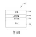
10:堆疊10: Stack
12:基材12: Substrate
14:膠黏層14: Adhesive layer
16:成核層16: Nucleation layer
18:金屬18: Metal
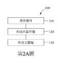
100:處理方法100: processing method
110、120、130、160:步驟110, 120, 130, 160: steps
125:去氣製程125: degassing process
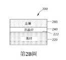
200:膜堆疊200: Membrane stack
220:基材220: Substrate
222:基材表面222: substrate surface
240:非晶矽層240: Amorphous silicon layer
260:膠黏層260: Adhesive layer
280:金屬層280: Metal layer
透過參考實施例(其中一些實施例繪示於附圖中),可得到上文簡要總結的本案揭露內容之更詳細之敘述,如此可詳細地瞭解本案揭露內容之上文所記載之特徵。然而,應注意附圖所說明的僅為本案揭露內容之典型實施例,因此不應被視為限制本案揭露內容之範疇,因為本案揭露內容可容許其他等效實施例。By referring to the embodiments (some of which are shown in the accompanying drawings), a more detailed description of the disclosure content of this case briefly summarized above can be obtained, so that the above-described features of the disclosure content of this case can be understood in detail. However, it should be noted that the drawings illustrated are only typical embodiments of the disclosure of this case, and therefore should not be regarded as limiting the scope of the disclosure of this case, because the disclosure of this case may allow other equivalent embodiments.
第1圖顯示根據本案揭露內容之一或多個實施例的膜堆疊之示意圖;第2A圖顯示根據本案揭露內容之一或多個實施例的製程方案;第2B圖顯示根據第2A圖之製程方案的膜堆疊之示意圖;第3圖顯示根據本案揭露內容之一或多個實施例的製程方案;第4A圖顯示根據本案揭露內容之一或多個實施例的製程方案;以及第4B圖顯示根據第4A圖之製程方案的膜堆疊之示意圖。Figure 1 shows a schematic diagram of a film stack according to one or more embodiments disclosed in this case; Figure 2A shows a process scheme according to one or more embodiments disclosed in this case; Figure 2B shows a process according to Figure 2A A schematic diagram of the film stack of the solution; Fig. 3 shows the process solution according to one or more embodiments disclosed in this case; Fig. 4A shows the process solution according to one or more embodiments disclosed in this case; and Fig. 4B shows A schematic diagram of the film stack according to the process scheme of Figure 4A.
描述本案揭露內容的數個示範性實施例之前,應了解本案揭露內容不限於下文的敘述中提出的構造或製程步驟之細節。本案揭露內容能實現其他實施例且以各種方式實行或執行。Before describing several exemplary embodiments of the disclosed content of this case, it should be understood that the disclosed content of this case is not limited to the details of the structure or process steps proposed in the following description. The content disclosed in this case can implement other embodiments and be implemented or executed in various ways.
如本文所用之「基材」是指任何基材或形成在基材上的材料表面,製造製程期間,膜處理是在該基材或該材料表面上執行。例如,取決於應用,上面可執行處理的基材表面包括諸如下述材料:矽、氧化矽、應變矽、絕緣體上覆矽(SOI)、摻雜碳的氧化矽、非晶矽、摻雜矽、鍺、砷化鎵、玻璃、藍寶石、及任何其他諸如金屬、金屬氮化物、金屬合金及其他導電材料之材料。基材包括半導體晶圓(此非限制)。基材可暴露至預處理製程,以研磨、蝕刻、還原、氧化、羥化、退火及/或烘烤基材表面。除了直接在基材本身表面上膜處理之外,在本案揭露內容中,所揭露的膜處理步驟中的任一者也可在下層上執行,該下層形成於該基材上,如下文中將更詳細揭露,且希望「基材表面」之用語包括如上下文所指之此下層。因此,例如,其中膜/層或部分膜/層已沉積在基材表面上時,新沉積的膜/層之暴露表面變成該基材表面。As used herein, "substrate" refers to any substrate or the surface of a material formed on a substrate. During the manufacturing process, film processing is performed on the substrate or the surface of the material. For example, depending on the application, the surface of the substrate that can be processed above includes materials such as: silicon, silicon oxide, strained silicon, silicon-on-insulator (SOI), carbon-doped silicon oxide, amorphous silicon, doped silicon , Germanium, gallium arsenide, glass, sapphire, and any other materials such as metals, metal nitrides, metal alloys and other conductive materials. The substrate includes a semiconductor wafer (this is not a limitation). The substrate can be exposed to a pretreatment process to grind, etch, reduce, oxidize, hydroxylate, anneal and/or bake the surface of the substrate. In addition to film processing directly on the surface of the substrate itself, in the disclosure of this case, any of the disclosed film processing steps can also be performed on the lower layer, which is formed on the substrate, as will be described later. It is disclosed in detail, and it is hoped that the term "substrate surface" includes this lower layer as the context refers to. Thus, for example, where the film/layer or part of the film/layer has been deposited on the surface of the substrate, the exposed surface of the newly deposited film/layer becomes the surface of the substrate.
如在此說明書中及申請專利範圍中所用,用語「前驅物」、「反應物」、「反應性氣體」、及類似物是可替換使用,以指可與基材表面反應的任何氣態物種。As used in this specification and in the scope of the patent application, the terms "precursor", "reactant", "reactive gas", and the like are used interchangeably to refer to any gaseous species that can react with the surface of the substrate.
本案揭露內容之一或多個實施例是針對沉積正形非晶矽薄膜之方法,該正形非晶矽薄膜作為下述之一或多者:膠黏層、氟擴散阻擋物及/或金屬ALD(例如,鎢沉積)的成核層。雖然在許多實施例中指涉鎢沉積,但發明所屬技術領域中具有通常知識者會了解,藉由揭露之製程可沉積其他金屬,例如鉬。本案揭露內容不限於ALD鎢沉積。One or more embodiments disclosed in this case are directed to a method for depositing a conformal amorphous silicon film, which serves as one or more of the following: an adhesive layer, a fluorine diffusion barrier, and/or a metal Nucleation layer for ALD (eg, tungsten deposition). Although many embodiments refer to tungsten deposition, those with ordinary knowledge in the technical field to which the invention belongs will understand that by disclosingThe process can deposit other metals, such as molybdenum. The disclosures in this case are not limited to ALD tungsten deposition.
本案揭露內容之實施例包括用於金屬ALD製程的製程整合方案。例如,鎢藉由原子層沉積而在矽基材上而沉積。參考第1圖,堆疊10可包括基材12(例如SiO2),具有膠黏層14(例如TiN)、成核層16(例如WSix及WBx)及金屬18(例如W)。製程方案的一或多個實施例中,成核層被非晶矽層置換。一些實施例中,成核層被非晶矽層置換且將TiN膠黏層做得較薄。一或多個實施例中,成核層與膠黏層兩者被非晶矽層置換。Examples of the disclosures in this case include process integration solutions for metal ALD processes. For example, tungsten is deposited on a silicon substrate by atomic layer deposition. Referring to FIG. 1, the
參考第2A圖與第2B圖,本案揭露內容之一或多個實施例是針對處理方法100與膜堆疊200。於步驟110,提供具有基材表面222的基材220。於步驟120,該基材220暴露至矽前驅物而在基材表面222上形成非晶矽層240。With reference to FIGS. 2A and 2B, one or more embodiments of the disclosure in this case are directed to the
一些實施例中,非晶矽(a-Si)形成可藉由使矽前驅物的分壓最大化,同時使晶圓溫度最小化而達成。適合的矽前驅物包括(但不限於)聚矽烷(SixHy)。例如,聚矽烷包括乙矽烷(Si2H6)、丙矽烷(Si3H8)、丁矽烷(Si4H10)、異丁矽烷、新戊矽烷(Si5H12)、環戊矽烷(Si5H10)、己矽烷(Si6H14)、環己矽烷(Si6H12)、或一般而言SixHy且x=2或更大,及上述前驅物之組合。例如,乙矽烷具有適中的處理溫度與高蒸氣壓,乙矽烷可單獨用作矽前驅物,或與其他物種相組合。In some embodiments, the formation of amorphous silicon (a-Si) can be achieved by maximizing the partial pressure of the silicon precursor while minimizing the wafer temperature. Suitable silicon precursors include, but are not limited to, polysilane (Six Hy ). For example, polysilanes include ethane (Si2 H6 ), propyl silane (Si3 H8 ), butane silane (Si4 H10 ), isobutane, neopentasilane (Si5 H12 ), cyclopentasilane ( Si5 H10 ), hexane (Si6 H14 ), cyclohexane (Si6 H12 ), or generally Six Hy and x=2 or greater, and combinations of the foregoing precursors. For example, disilane has a moderate processing temperature and high vapor pressure, and disilane can be used as a silicon precursor alone or in combination with other species.
一些實施例中,矽前驅物實質上僅包括乙矽烷。如在此說明書及所附申請專利範圍中所用,詞彙「實質上僅……乙矽烷」意味至少95%的活性物種是乙矽烷。可納入任何量的其他氣體,諸如載氣及惰性氣體。In some embodiments, the silicon precursor consists essentially only of disilane. As used in this specification and the scope of the attached patent application, the term "substantially only... ethane" means that at least 95% of the active species is ethane. Any amount of other gases, such as carrier gas and inert gas, can be included.
非晶矽層240的厚度可取決於例如基材表面及後續的膜與製程而有所不同。一些實施例中,非晶矽層240具有範圍在約1埃至約100埃的厚度。一或多個實施例中,非晶矽層240具有範圍在約1埃至約50埃、或範圍在約10埃至約40埃、或範圍在約30埃至約40埃的厚度。一些實施例中,非晶矽層240的厚度大於0埃且小於或等於約50埃、45埃、或40埃。The thickness of the
於步驟130,金屬層280形成在非晶矽層240上。金屬層280可藉由任何適合的技術形成,該技術包括(但不限於)原子層沉積(ALD)、電漿增強原子層沉積(PE-ALD)、化學氣相沉積(CVD)、電漿增強化學氣相沉積(PE-CVD)與物理氣相沉積(PVD)。In
金屬層280可包括任何適合的金屬。一些實施例中,金屬層280包括鎢或鉬之一或多者。一些實施例中,金屬層280基本上由鎢組成。一些實施例中,金屬層280基本上由鉬組成。如在此方面所用,「基本上由......組成」意味著該金屬層280包括大於或等於約80、85、90、或95原子%的指定成分。例如,基本上由鎢組成的金屬層280具有大於或等於約例如90原子%的鎢的組成物。The
一些實施例中,金屬層280由CVD沉積。金屬前驅物與反應物可共同流進處理腔室,以在基材上沉積層。該前驅物與反應物得以在氣相中反應。In some embodiments, the
一些實施例中,金屬層280由ALD沉積。在時域(time-domain)ALD製程中,金屬前驅物流進處理腔室而與表面反應。沖洗腔室除去過多前驅物及副產物,且該反應物流進腔室中。該前驅物及反應物並非同時在處理腔室中,所以極少(或無)氣相反應。空間ALD製程中,金屬前驅物流進處理腔室的第一區段,而反應物同時流進處理腔室的第二區段。該第一區段與該第二區段被氣簾分開,以防止前驅物與反應物之間的氣相反應。基材在第一區段及第二區段之間移動,以依序地將表面暴露至前驅物及反應物。一些實施例中,金屬層280是透過依序將非晶矽層240暴露至金屬前驅物及反應物而沉積。In some embodiments, the
金屬前驅物可以是可用於沉積金屬膜的任何適合的前驅物。一些實施例中,金屬前驅物包括一金屬,該金屬是選自鎢、鉬、及前述金屬之組合。一或多個實施例中,金屬前驅物包括WF6及MoF6之一或多者。一些實施例中,該金屬前驅物是含氟前驅物。已知氟可蝕刻矽表面。本案揭露內容之一些實施例有利地容許使用氟前驅物,因為該非晶矽層240可形成至足以確保該前驅物不移除所有a-Si膜的厚度。The metal precursor can be any suitable precursor that can be used to deposit metal films. In some embodiments, the metal precursor includes a metal selected from tungsten, molybdenum, and combinations of the foregoing metals. In one or more embodiments, the metal precursor includes one or more of WF6 and MoF6 . In some embodiments, the metal precursor is a fluorine-containing precursor. It is known that fluorine can etch the surface of silicon. Some embodiments of the present disclosure advantageously allow the use of a fluorine precursor because the
該反應物可為能夠與表面上形成之物種反應的任何適合的反應物。例如,若使用WF6作為前驅物,則表面上會有WFx物種。該反應物能夠與-WFx物種反應,而產生鎢膜。The reactant can be any suitable reactant capable of reacting with the species formed on the surface. For example, if WF6 is used as a precursor, there will be WFx species on the surface. The reactant can react with the -WFx species to produce a tungsten film.
第3圖顯示本案揭露內容之另一實施例的流程,其中在形成非晶矽層240之後納入去氣(degas)製程125。一些實施例中的非晶矽層240暴露至去氣環境,以在形成該金屬層280之前移除釋氣(outgas)的物種。FIG. 3 shows the process of another embodiment of the disclosure of this case, in which a
沉積的非晶矽層240可散發或釋氣一物種,該物種例如氫。去氣環境提供氣態物種散發的機會,從而將最終膜的起泡減至最小。去氣環境可包括任何條件,容許或激勵膜去氣。例如,去氣環境可基本上由惰性氣體組成。如在這方面所用,「基本上由……組成」意味著沒有干擾沉積之膜的釋氣的氣態物種。可存在其他反應性物種,只要不抑制膜之去氣且同時仍基本上由惰性氣體組成即可。The deposited
適合的惰性氣體包括(但不限於)氬、氦、氮、及/或前述氣體之混合物的一或多者。Suitable inert gases include (but are not limited to) one or more of argon, helium, nitrogen, and/or mixtures of the foregoing gases.
一或多個實施例中,釋氣的物種包括氫、SiH2、SiH3、SiH4、及/或其他低階矽烷。In one or more embodiments, the outgassing species includes hydrogen, SiH2 , SiH3 , SiH4 , and/or other low-order silanes.
處理腔室中或處理腔室的區域中的壓力可獨立受控以用於前驅物暴露及去氣環境。在一些實施例中,對於矽前驅物及去氣環境之各者的暴露發生在範圍為約10毫托至約100托的壓力下。一些實施例中,矽前驅物於大於或等於約500毫托的壓力暴露至基材,該壓力或者為大於或等於約1托、或者為大於或等於約5托、或者為大於或等於約10托、或者為大於或等於約20托、或者為大於或等於約30托。The pressure in the processing chamber or in the area of the processing chamber can be independently controlled for precursor exposure and degassing environments. In some embodiments, exposure to each of the silicon precursor and the degassing environment occurs at a pressure ranging from about 10 millitorr to about 100 Torr. In some embodiments, the silicon precursor is exposed to the substrate at a pressure greater than or equal to about 500 millitorr, and the pressure is either greater than or equal to about 1 torr, or greater than or equal to about 5 torr, orIt is greater than or equal to about 10 Torr, or greater than or equal to about 20 Torr, or greater than or equal to about 30 Torr.
基材表面暴露至前驅物或去氣環境的溫度可取決於前驅物及形成的元件之熱預算而有所不同。一些實施例中,對於前驅物及去氣環境之各者的暴露發生在範圍為約攝氏100度至約攝氏700度的溫度下。一或多個實施例中,鹵化矽前驅物於範圍為約攝氏250度至約攝氏600度、或範圍為約攝氏400度至約攝氏550度的溫度暴露至基材。The temperature at which the surface of the substrate is exposed to the precursor or degassing environment may vary depending on the thermal budget of the precursor and the formed device. In some embodiments, exposure to each of the precursor and the degassing environment occurs at a temperature ranging from about 100 degrees Celsius to about 700 degrees Celsius. In one or more embodiments, the silicon halide precursor is exposed to the substrate at a temperature ranging from about 250 degrees Celsius to about 600 degrees Celsius, or from about 400 degrees Celsius to about 550 degrees Celsius.
可修改暴露至去氣環境之前以矽前驅物形成的a-Si膜之厚度。一些實施例中,對於矽前驅物及去氣環境之各者的暴露生長範圍為約5埃至約20埃的厚度的膜。The thickness of the a-Si film formed with the silicon precursor before exposure to the degassing environment can be modified. In some embodiments, the exposed growth range for each of the silicon precursor and the degassing environment is about 5 angstroms to about 20 angstroms in thickness.
前驅物與去氣環境可重複、依序地暴露至基材表面,而形成具預定厚度的膜。一些實施例中,非晶矽膜具有範圍為約100埃至約1微米之總厚度。The precursor and the degassing environment can be repeatedly and sequentially exposed to the surface of the substrate to form a film with a predetermined thickness. In some embodiments, the amorphous silicon film has a total thickness ranging from about 100 angstroms to about 1 micrometer.
一些實施例中,a-Si是由乙矽烷於低於約攝氏450度的晶圓溫度沉積,且乙矽烷分壓大於或等於約20托。示範性實施例中,基材於大於或等於約20托的壓力及範圍為約攝氏400度至約攝氏550度的溫度暴露至矽前驅物。In some embodiments, a-Si is deposited from ethane at a wafer temperature lower than about 450 degrees Celsius, and the partial pressure of ethane is greater than or equal to about 20 Torr. In an exemplary embodiment, the substrate is exposed to the silicon precursor at a pressure greater than or equal to about 20 Torr and a temperature ranging from about 400 degrees Celsius to about 550 degrees Celsius.
參考第4A圖與第4B圖,本案揭露內容之一些實施例進一步包括步驟160,其中於形成非晶矽層240之前將膠黏層260沉積在基材上。該膠黏層260是非晶矽可黏著之層,且相較於該非晶矽直接沉積於基材220上的情況,該非晶矽黏著至該膠黏層是較不可能剝落的。一些實施例中,該膠黏層包括TiN。一或多個實施例中,基材220具有氧化物表面,且膠黏層包括TiN。Referring to FIGS. 4A and 4B, some embodiments disclosed in this case further include
膠黏層260之厚度可取決於待沉積之非晶矽之厚度及基材而有所不同。一些實施例中,該膠黏層260之厚度在約1埃至約30埃之範圍內,或在約5埃至約30埃之範圍內。一些實施例中,該膠黏層260之厚度小於或等於約20埃、或者小於或等於約15埃,或者小於或等於約10埃,或者小於或等於約5埃。The thickness of the
參考第4B圖,本案揭露內容之一或多個實施例是針對堆疊200,該堆疊200包括基材220,該基材220具有氧化物表面222。膠黏層260位在該氧化物表面222上。一些實施例的膠黏層包括TiN,且厚度在約5埃至約30埃之範圍內。非晶矽層240位於膠黏層260上,且具有範圍為約5埃至約50埃的厚度。金屬層280位在非晶矽層240上且包括鎢與鉬之一或多者。Referring to FIG. 4B, one or more of the embodiments disclosed in this case are directed to the
根據一或多個實施例,在形成該層之前及/或之後,該基材經受處理。此處理可在相同腔室中或在一或多個分開(separate)的處理腔室中執行。一些實施例中,基材從第一腔室移動到分開的第二腔室以進一步處理。該基材可直接從第一腔室移動到分開的處理腔室,或該基材可從第一腔室移動到一或多個移送腔室,然後移動到分開的處理腔室。因此,處理設備可包括與移送站相連的多個腔室。此類的設備可稱為「群集工具」或「群集的系統」等。According to one or more embodiments, the substrate is subjected to treatment before and/or after forming the layer. This treatment can be performed in the same chamber or in one or more separate treatment chambers. In some embodiments, the substrate is moved from the first chamber to a separate second chamber for further processing. The substrate can be moved directly from the first chamber to a separate processing chamber, or the substrate can be moved from the first chamber to one or more transfer chambers and then to a separate processing chamber. Therefore, the processing equipment may include a connection to the transfer stationOf multiple chambers. Such equipment can be called "cluster tool" or "clustered system", etc.
大體上,群集工具是包括多個腔室的模組系統,該等腔室執行各種功能,包括基材定心(center-finding)及定向、去氣、退火、沉積及/或蝕刻。根據一或多個實施例,群集工具包括至少第一腔室與中央移送腔室。該中央移送腔室可容置機器人,該機器人能夠在處理腔室及裝載閘腔室之間來回傳送基材。該移送腔室一般是維持在真空條件,且提供中繼平台以將基材從一個腔室來回傳送至另一腔室及/或裝載閘腔室,該裝載閘腔室定位在群集工具的前端。可適於本案揭露內容的兩種已知的群集工具是Centura®及Endura®,上述兩者皆可得自美國加州Santa Clara的應用材料公司。然而,可調整確切的腔室排列及組合,以執行如本文所述之製程的特定步驟。可使用的其他處理腔室包括(但不限於)用於執行下述製程的腔室:循環層沉積(CLD)、原子層沉積(ALD)、化學氣相沉積(CVD)、物理氣相沉積(PVD)、蝕刻、預清潔、化學清潔、熱處理(諸如RTP)、電漿氮化、去氣、定向、羥化、及/或其他基材製程。透過在群集工具上的腔室中執行製程,可避免具大氣雜質的基材表面污染而無須在沉積後續膜之前氧化。In general, the cluster tool is a modular system that includes multiple chambers that perform various functions including center-finding and orientation, degassing, annealing, deposition, and/or etching. According to one or more embodiments, the cluster tool includes at least a first chamber and a central transfer chamber. The central transfer chamber can accommodate a robot that can transfer substrates back and forth between the processing chamber and the loading lock chamber. The transfer chamber is generally maintained in a vacuum condition, and a relay platform is provided to transfer substrates from one chamber to another and/or a load lock chamber, which is positioned at the front end of the cluster tool . Two known clustering tools that can be adapted to the disclosure of this case are Centura® and Endura®, both of which are available from Applied Materials of Santa Clara, California. However, the exact chamber arrangement and combination can be adjusted to perform specific steps of the process as described herein. Other processing chambers that can be used include (but are not limited to) chambers for performing the following processes: cyclic layer deposition (CLD), atomic layer deposition (ALD), chemical vapor deposition (CVD), physical vapor deposition ( PVD), etching, pre-cleaning, chemical cleaning, heat treatment (such as RTP), plasma nitriding, degassing, orientation, hydroxylation, and/or other substrate manufacturing processes. By performing the process in the chamber on the cluster tool, contamination of the substrate surface with atmospheric impurities can be avoided without the need for oxidation before deposition of subsequent films.
根據一或多個實施例,基材連續地處於真空下或「裝載鎖定」條件,且當從一個腔室移動到下一個時不暴露至周圍空氣。從而移送腔室處於真空下且於真空壓力下泵送降壓(pump down)。惰性氣體可存在於處理腔室或移送腔室中。一些實施例中,惰性氣體用作為沖洗氣體,以移除一些或所有反應物。根據一或多個實施例,於沉積腔室之出口注射沖洗氣體,以防止反應物從該沉積腔室移動到移送腔室及/或額外的處理腔室。從而惰性氣體流在該腔室之出口形成簾幕。According to one or more embodiments, the substrate is continuously under vacuum or "load-locked" conditions and is not exposed to ambient air when moving from one chamber to the next. So that the transfer chamber is under vacuum and under vacuum pressurePump down. The inert gas may be present in the processing chamber or the transfer chamber. In some embodiments, an inert gas is used as a flushing gas to remove some or all of the reactants. According to one or more embodiments, flushing gas is injected at the outlet of the deposition chamber to prevent the reactants from moving from the deposition chamber to the transfer chamber and/or additional processing chambers. The inert gas flow forms a curtain at the outlet of the chamber.
可在單一基材沉積腔室中處理基材,其中裝載、處理、及卸載單一基材,之後再處理另一基材。也可用連續方式(類似輸送器(conveyor)系統)處理該基材,其中多個基材個別裝載到腔室的第一部分中,移動通過該腔室,從該腔室的第二部分卸載。該腔室及相關輸送器系統的形狀可形成筆直路徑或彎曲路徑。此外,該處理腔室可以是旋轉料架(carousel),其中多個基材繞中心軸移動,且在整個旋轉料架路徑中暴露至沉積、蝕刻、退火、清潔等製程。The substrate can be processed in a single substrate deposition chamber, where a single substrate is loaded, processed, and unloaded, and then another substrate is processed. The substrate can also be processed in a continuous manner (similar to a conveyor system), where multiple substrates are individually loaded into the first part of the chamber, moved through the chamber, and unloaded from the second part of the chamber. The shape of the chamber and related conveyor system can form a straight path or a curved path. In addition, the processing chamber may be a carousel, in which a plurality of substrates move around a central axis and are exposed to deposition, etching, annealing, cleaning and other processes in the entire path of the carousel.
處理期間,可加熱或冷卻基材。此加熱或冷卻可透過任何適合的手段完成,該手段包括(但不限於)改變基材支撐件的溫度且將經加熱或冷卻之氣體流至基材表面。一些實施例中,該基材支撐件包括加熱器/冷卻器,可控制該加熱器/冷卻器以傳導式改變基材溫度。一或多個實施例中,所運用的該等氣體(無論是反應性氣體或是惰性氣體)經加熱或冷卻以局部改變基材溫度。一些實施例中,加熱器/冷卻器定位在腔室內鄰近基材表面,以對流式改變基材溫度。During processing, the substrate can be heated or cooled. This heating or cooling can be accomplished by any suitable means, including (but not limited to) changing the temperature of the substrate support and flowing heated or cooled gas to the surface of the substrate. In some embodiments, the substrate support includes a heater/cooler, and the heater/cooler can be controlled to conductively change the temperature of the substrate. In one or more embodiments, the gases used (whether reactive gas or inert gas) are heated or cooled to locally change the substrate temperature. In some embodiments, the heater/cooler is positioned in the chamber adjacent to the surface of the substrate to convectively change the temperature of the substrate.
該基材在處理期間也可為靜態或旋轉。旋轉基材可連續地或以分開的步驟旋轉。例如,基材可在整個製程中旋轉,或該基材可在暴露至不同反應性氣體或沖洗氣體之間旋轉少量。處理期間旋轉基材(無論是連續式或多步式)可透過將例如氣流幾何中的局部變化性之效應減至最小而助於產生更均勻的沉積或蝕刻。The substrate can also be static or rotating during processing. The rotating substrate can be rotated continuously or in separate steps. For example, the substrate can be rotated throughout the process, or the substrate can be rotated a small amount between exposure to different reactive gases or flushing gases. Rotating the substrate (whether continuous or multi-step) during processing can help produce more uniform deposition or etching by minimizing effects such as local variability in gas flow geometry.
原子層沉積類型的腔室中,無論是空間上或時間上分開的製程,基材可暴露至第一前驅物與第二前驅物。時間式ALD是其中第一前驅物流進腔室與表面反應的傳統製程。使第二前驅物流入之前,先從腔室沖洗該第一前驅物。在空間式ALD中,第一前驅物與第二前驅物同時流至該腔室但在空間上分開,使得在該等前驅物流之間有防止前驅物混合的區域。在空間式ALD中,基材相對於氣體分配板移動,反之亦然。In an atomic layer deposition type chamber, whether it is a spatially or temporally separated process, the substrate can be exposed to the first precursor and the second precursor. Time-based ALD is a traditional process in which the first precursor flows into the chamber to react with the surface. Before the second precursor flows in, the first precursor is flushed from the chamber. In the spatial ALD, the first precursor and the second precursor flow to the chamber at the same time but are separated in space, so that there is a region between the precursor streams that prevents the precursors from mixing. In spatial ALD, the substrate moves relative to the gas distribution plate, and vice versa.
其中該等方法的多個部分的一或多者發生在一個腔室中的多個實施例中,該製程可以是空間式ALD製程。儘管上文描述的化學條件的一或多者可能不相容(即,造成基材表面上以外的反應及/或腔室上的沉積),空間上的分開確保試劑不會暴露至氣相中的各者。例如,時間式ALD涉及沖洗沉積腔室。但是,在實務上,有時不可能在以另外的試劑流動之前先將過量試劑沖洗出腔室。因此,在該腔室中的任何殘存試劑可能反應。以空間上的分開,則過量試劑不需要被沖洗掉,且限制了交叉污染。再者,可能會使用許多時間沖洗腔室,所以可透過消除沖洗步驟而增加產率。In multiple embodiments where one or more of the multiple parts of the methods occur in one chamber, the process may be a spatial ALD process. Although one or more of the chemical conditions described above may be incompatible (ie, cause reactions outside the substrate surface and/or deposition on the chamber), the spatial separation ensures that the reagents are not exposed to the gas phase Of each. For example, temporal ALD involves flushing the deposition chamber. However, in practice, it is sometimes impossible to flush excess reagent out of the chamber before flowing another reagent. Therefore, any remaining reagents in the chamber may react. With spatial separation, excess reagent does not need to be washed away, and cross-contamination is limiteddye. Furthermore, it may take a lot of time to flush the chamber, so the productivity can be increased by eliminating the flushing step.
這整份說明書中對「一個實施例」、「某些實施例」、「一或多個實施例」、或「一實施例」的參考意味著在本案揭露內容的至少一個實施例中包括了與該實施例相關的所述特定特徵、結構、材料、或特性。因此這整份說明書中多處出現的諸如「在一或多個實施例中」、「在某些實施例中」、「在一或多個實施例中」、或「在一實施例中」之詞彙並非必然指本案揭露內容的相同實施例。再者,於一或多個實施例中可以任何適合的方式組合特定特徵、結構、材料、或特性。References in this entire specification to “one embodiment”, “certain embodiments”, “one or more embodiments”, or “one embodiment” means that at least one embodiment of the disclosure in this case includes The specific feature, structure, material, or characteristic related to this embodiment. Therefore, in many places throughout this specification, such as "in one or more embodiments", "in some embodiments", "in one or more embodiments", or "in an embodiment" The vocabulary does not necessarily refer to the same embodiment of the content disclosed in this case. Furthermore, specific features, structures, materials, or characteristics can be combined in any suitable manner in one or more embodiments.
儘管已參考特定實施例描述本文的揭露,但應了解這些實施例僅是說明本案揭露內容的原理與應用。對發明所屬技術領域中具有通常知識者而言可明瞭,能夠對本案揭露內容之方法與設備製作各種修飾例與變化例但不可背離本案揭露內容之精神與範疇。因此,希望本案揭露內容包括在所附之申請專利範圍與其等效例的範疇內的修飾例及變化例。Although the disclosure in this document has been described with reference to specific embodiments, it should be understood that these embodiments only illustrate the principles and applications of the disclosure in this case. It is obvious to those with ordinary knowledge in the technical field to which the invention belongs, that various modifications and variations can be made to the method and equipment of the disclosure of the case without departing from the spirit and scope of the disclosure of the case. Therefore, it is hoped that the disclosure of this case includes modifications and variations within the scope of the attached patent application and its equivalents.
200‧‧‧膜堆疊200‧‧‧Membrane stack
220‧‧‧基材220‧‧‧Substrate
222‧‧‧基材表面222‧‧‧Substrate surface
240‧‧‧非晶矽層240‧‧‧Amorphous silicon layer
260‧‧‧膠黏層260‧‧‧Adhesive layer
280‧‧‧金屬層280‧‧‧Metal layer
Claims (15)
Translated fromChineseApplications Claiming Priority (2)
| Application Number | Priority Date | Filing Date | Title |
|---|---|---|---|
| US201562269974P | 2015-12-19 | 2015-12-19 | |
| US62/269,974 | 2015-12-19 |
Publications (2)
| Publication Number | Publication Date |
|---|---|
| TW201728775A TW201728775A (en) | 2017-08-16 |
| TWI716511Btrue TWI716511B (en) | 2021-01-21 |
Family
ID=59057786
Family Applications (1)
| Application Number | Title | Priority Date | Filing Date |
|---|---|---|---|
| TW105141140ATWI716511B (en) | 2015-12-19 | 2016-12-13 | Conformal amorphous silicon as nucleation layer for w ald process |
Country Status (5)
| Country | Link |
|---|---|
| US (1) | US9978685B2 (en) |
| KR (2) | KR102866666B1 (en) |
| CN (1) | CN108369897B (en) |
| TW (1) | TWI716511B (en) |
| WO (1) | WO2017106660A1 (en) |
Families Citing this family (288)
| Publication number | Priority date | Publication date | Assignee | Title |
|---|---|---|---|---|
| US20130023129A1 (en) | 2011-07-20 | 2013-01-24 | Asm America, Inc. | Pressure transmitter for a semiconductor processing environment |
| US10714315B2 (en) | 2012-10-12 | 2020-07-14 | Asm Ip Holdings B.V. | Semiconductor reaction chamber showerhead |
| US20160376700A1 (en) | 2013-02-01 | 2016-12-29 | Asm Ip Holding B.V. | System for treatment of deposition reactor |
| US11015245B2 (en) | 2014-03-19 | 2021-05-25 | Asm Ip Holding B.V. | Gas-phase reactor and system having exhaust plenum and components thereof |
| US10941490B2 (en) | 2014-10-07 | 2021-03-09 | Asm Ip Holding B.V. | Multiple temperature range susceptor, assembly, reactor and system including the susceptor, and methods of using the same |
| US10276355B2 (en) | 2015-03-12 | 2019-04-30 | Asm Ip Holding B.V. | Multi-zone reactor, system including the reactor, and method of using the same |
| US10458018B2 (en) | 2015-06-26 | 2019-10-29 | Asm Ip Holding B.V. | Structures including metal carbide material, devices including the structures, and methods of forming same |
| US10211308B2 (en) | 2015-10-21 | 2019-02-19 | Asm Ip Holding B.V. | NbMC layers |
| US10480066B2 (en) | 2015-12-19 | 2019-11-19 | Applied Materials, Inc. | Metal deposition methods |
| US10991586B2 (en) | 2015-12-19 | 2021-04-27 | Applied Materials, Inc. | In-situ tungsten deposition without barrier layer |
| US10468263B2 (en) | 2015-12-19 | 2019-11-05 | Applied Materials, Inc. | Tungsten deposition without barrier layer |
| US11139308B2 (en) | 2015-12-29 | 2021-10-05 | Asm Ip Holding B.V. | Atomic layer deposition of III-V compounds to form V-NAND devices |
| US10529554B2 (en) | 2016-02-19 | 2020-01-07 | Asm Ip Holding B.V. | Method for forming silicon nitride film selectively on sidewalls or flat surfaces of trenches |
| US10343920B2 (en) | 2016-03-18 | 2019-07-09 | Asm Ip Holding B.V. | Aligned carbon nanotubes |
| US10367080B2 (en) | 2016-05-02 | 2019-07-30 | Asm Ip Holding B.V. | Method of forming a germanium oxynitride film |
| US11453943B2 (en) | 2016-05-25 | 2022-09-27 | Asm Ip Holding B.V. | Method for forming carbon-containing silicon/metal oxide or nitride film by ALD using silicon precursor and hydrocarbon precursor |
| US9859151B1 (en) | 2016-07-08 | 2018-01-02 | Asm Ip Holding B.V. | Selective film deposition method to form air gaps |
| US10612137B2 (en) | 2016-07-08 | 2020-04-07 | Asm Ip Holdings B.V. | Organic reactants for atomic layer deposition |
| US9812320B1 (en) | 2016-07-28 | 2017-11-07 | Asm Ip Holding B.V. | Method and apparatus for filling a gap |
| KR102532607B1 (en) | 2016-07-28 | 2023-05-15 | 에이에스엠 아이피 홀딩 비.브이. | Substrate processing apparatus and method of operating the same |
| US9887082B1 (en) | 2016-07-28 | 2018-02-06 | Asm Ip Holding B.V. | Method and apparatus for filling a gap |
| US11532757B2 (en) | 2016-10-27 | 2022-12-20 | Asm Ip Holding B.V. | Deposition of charge trapping layers |
| US10714350B2 (en) | 2016-11-01 | 2020-07-14 | ASM IP Holdings, B.V. | Methods for forming a transition metal niobium nitride film on a substrate by atomic layer deposition and related semiconductor device structures |
| KR102546317B1 (en) | 2016-11-15 | 2023-06-21 | 에이에스엠 아이피 홀딩 비.브이. | Gas supply unit and substrate processing apparatus including the same |
| KR102762543B1 (en) | 2016-12-14 | 2025-02-05 | 에이에스엠 아이피 홀딩 비.브이. | Substrate processing apparatus |
| US11447861B2 (en) | 2016-12-15 | 2022-09-20 | Asm Ip Holding B.V. | Sequential infiltration synthesis apparatus and a method of forming a patterned structure |
| US11581186B2 (en) | 2016-12-15 | 2023-02-14 | Asm Ip Holding B.V. | Sequential infiltration synthesis apparatus |
| KR102700194B1 (en) | 2016-12-19 | 2024-08-28 | 에이에스엠 아이피 홀딩 비.브이. | Substrate processing apparatus |
| US10269558B2 (en) | 2016-12-22 | 2019-04-23 | Asm Ip Holding B.V. | Method of forming a structure on a substrate |
| US10867788B2 (en)* | 2016-12-28 | 2020-12-15 | Asm Ip Holding B.V. | Method of forming a structure on a substrate |
| US11390950B2 (en) | 2017-01-10 | 2022-07-19 | Asm Ip Holding B.V. | Reactor system and method to reduce residue buildup during a film deposition process |
| US10468261B2 (en) | 2017-02-15 | 2019-11-05 | Asm Ip Holding B.V. | Methods for forming a metallic film on a substrate by cyclical deposition and related semiconductor device structures |
| US10529563B2 (en) | 2017-03-29 | 2020-01-07 | Asm Ip Holdings B.V. | Method for forming doped metal oxide films on a substrate by cyclical deposition and related semiconductor device structures |
| US10770286B2 (en) | 2017-05-08 | 2020-09-08 | Asm Ip Holdings B.V. | Methods for selectively forming a silicon nitride film on a substrate and related semiconductor device structures |
| US12040200B2 (en) | 2017-06-20 | 2024-07-16 | Asm Ip Holding B.V. | Semiconductor processing apparatus and methods for calibrating a semiconductor processing apparatus |
| US11306395B2 (en) | 2017-06-28 | 2022-04-19 | Asm Ip Holding B.V. | Methods for depositing a transition metal nitride film on a substrate by atomic layer deposition and related deposition apparatus |
| KR20190009245A (en) | 2017-07-18 | 2019-01-28 | 에이에스엠 아이피 홀딩 비.브이. | Methods for forming a semiconductor device structure and related semiconductor device structures |
| US10541333B2 (en) | 2017-07-19 | 2020-01-21 | Asm Ip Holding B.V. | Method for depositing a group IV semiconductor and related semiconductor device structures |
| US11374112B2 (en) | 2017-07-19 | 2022-06-28 | Asm Ip Holding B.V. | Method for depositing a group IV semiconductor and related semiconductor device structures |
| US11018002B2 (en) | 2017-07-19 | 2021-05-25 | Asm Ip Holding B.V. | Method for selectively depositing a Group IV semiconductor and related semiconductor device structures |
| US10590535B2 (en) | 2017-07-26 | 2020-03-17 | Asm Ip Holdings B.V. | Chemical treatment, deposition and/or infiltration apparatus and method for using the same |
| TWI815813B (en) | 2017-08-04 | 2023-09-21 | 荷蘭商Asm智慧財產控股公司 | Showerhead assembly for distributing a gas within a reaction chamber |
| US10692741B2 (en) | 2017-08-08 | 2020-06-23 | Asm Ip Holdings B.V. | Radiation shield |
| US10770336B2 (en) | 2017-08-08 | 2020-09-08 | Asm Ip Holding B.V. | Substrate lift mechanism and reactor including same |
| US11769682B2 (en) | 2017-08-09 | 2023-09-26 | Asm Ip Holding B.V. | Storage apparatus for storing cassettes for substrates and processing apparatus equipped therewith |
| US11139191B2 (en) | 2017-08-09 | 2021-10-05 | Asm Ip Holding B.V. | Storage apparatus for storing cassettes for substrates and processing apparatus equipped therewith |
| US11830730B2 (en) | 2017-08-29 | 2023-11-28 | Asm Ip Holding B.V. | Layer forming method and apparatus |
| KR102491945B1 (en) | 2017-08-30 | 2023-01-26 | 에이에스엠 아이피 홀딩 비.브이. | Substrate processing apparatus |
| US11295980B2 (en) | 2017-08-30 | 2022-04-05 | Asm Ip Holding B.V. | Methods for depositing a molybdenum metal film over a dielectric surface of a substrate by a cyclical deposition process and related semiconductor device structures |
| US11056344B2 (en) | 2017-08-30 | 2021-07-06 | Asm Ip Holding B.V. | Layer forming method |
| US10658205B2 (en) | 2017-09-28 | 2020-05-19 | Asm Ip Holdings B.V. | Chemical dispensing apparatus and methods for dispensing a chemical to a reaction chamber |
| US10403504B2 (en) | 2017-10-05 | 2019-09-03 | Asm Ip Holding B.V. | Method for selectively depositing a metallic film on a substrate |
| KR20200052994A (en)* | 2017-10-09 | 2020-05-15 | 어플라이드 머티어리얼스, 인코포레이티드 | Conformal doped amorphous silicon as nucleation layer for metal deposition |
| US10923344B2 (en) | 2017-10-30 | 2021-02-16 | Asm Ip Holding B.V. | Methods for forming a semiconductor structure and related semiconductor structures |
| US11022879B2 (en) | 2017-11-24 | 2021-06-01 | Asm Ip Holding B.V. | Method of forming an enhanced unexposed photoresist layer |
| CN111344522B (en) | 2017-11-27 | 2022-04-12 | 阿斯莫Ip控股公司 | Including clean mini-environment device |
| WO2019103613A1 (en) | 2017-11-27 | 2019-05-31 | Asm Ip Holding B.V. | A storage device for storing wafer cassettes for use with a batch furnace |
| US10872771B2 (en) | 2018-01-16 | 2020-12-22 | Asm Ip Holding B. V. | Method for depositing a material film on a substrate within a reaction chamber by a cyclical deposition process and related device structures |
| TWI799494B (en) | 2018-01-19 | 2023-04-21 | 荷蘭商Asm 智慧財產控股公司 | Deposition method |
| KR102695659B1 (en) | 2018-01-19 | 2024-08-14 | 에이에스엠 아이피 홀딩 비.브이. | Method for depositing a gap filling layer by plasma assisted deposition |
| US11081345B2 (en) | 2018-02-06 | 2021-08-03 | Asm Ip Holding B.V. | Method of post-deposition treatment for silicon oxide film |
| US10896820B2 (en) | 2018-02-14 | 2021-01-19 | Asm Ip Holding B.V. | Method for depositing a ruthenium-containing film on a substrate by a cyclical deposition process |
| WO2019158960A1 (en) | 2018-02-14 | 2019-08-22 | Asm Ip Holding B.V. | A method for depositing a ruthenium-containing film on a substrate by a cyclical deposition process |
| US10731249B2 (en) | 2018-02-15 | 2020-08-04 | Asm Ip Holding B.V. | Method of forming a transition metal containing film on a substrate by a cyclical deposition process, a method for supplying a transition metal halide compound to a reaction chamber, and related vapor deposition apparatus |
| KR102636427B1 (en) | 2018-02-20 | 2024-02-13 | 에이에스엠 아이피 홀딩 비.브이. | Substrate processing method and apparatus |
| JP7072399B2 (en)* | 2018-02-21 | 2022-05-20 | 東京エレクトロン株式会社 | Tungsten film film forming method, film forming system and storage medium |
| US10975470B2 (en) | 2018-02-23 | 2021-04-13 | Asm Ip Holding B.V. | Apparatus for detecting or monitoring for a chemical precursor in a high temperature environment |
| US11473195B2 (en) | 2018-03-01 | 2022-10-18 | Asm Ip Holding B.V. | Semiconductor processing apparatus and a method for processing a substrate |
| US11629406B2 (en) | 2018-03-09 | 2023-04-18 | Asm Ip Holding B.V. | Semiconductor processing apparatus comprising one or more pyrometers for measuring a temperature of a substrate during transfer of the substrate |
| US11114283B2 (en) | 2018-03-16 | 2021-09-07 | Asm Ip Holding B.V. | Reactor, system including the reactor, and methods of manufacturing and using same |
| KR102646467B1 (en) | 2018-03-27 | 2024-03-11 | 에이에스엠 아이피 홀딩 비.브이. | Method of forming an electrode on a substrate and a semiconductor device structure including an electrode |
| US11230766B2 (en) | 2018-03-29 | 2022-01-25 | Asm Ip Holding B.V. | Substrate processing apparatus and method |
| US11088002B2 (en) | 2018-03-29 | 2021-08-10 | Asm Ip Holding B.V. | Substrate rack and a substrate processing system and method |
| KR102600229B1 (en) | 2018-04-09 | 2023-11-10 | 에이에스엠 아이피 홀딩 비.브이. | Substrate supporting device, substrate processing apparatus including the same and substrate processing method |
| SG11202009514WA (en)* | 2018-04-24 | 2020-11-27 | Applied Materials Inc | Tungsten deposition without barrier layer |
| US12025484B2 (en) | 2018-05-08 | 2024-07-02 | Asm Ip Holding B.V. | Thin film forming method |
| TWI811348B (en) | 2018-05-08 | 2023-08-11 | 荷蘭商Asm 智慧財產控股公司 | Methods for depositing an oxide film on a substrate by a cyclical deposition process and related device structures |
| US12272527B2 (en) | 2018-05-09 | 2025-04-08 | Asm Ip Holding B.V. | Apparatus for use with hydrogen radicals and method of using same |
| KR102596988B1 (en) | 2018-05-28 | 2023-10-31 | 에이에스엠 아이피 홀딩 비.브이. | Method of processing a substrate and a device manufactured by the same |
| TWI840362B (en) | 2018-06-04 | 2024-05-01 | 荷蘭商Asm Ip私人控股有限公司 | Wafer handling chamber with moisture reduction |
| US11718913B2 (en) | 2018-06-04 | 2023-08-08 | Asm Ip Holding B.V. | Gas distribution system and reactor system including same |
| US11286562B2 (en) | 2018-06-08 | 2022-03-29 | Asm Ip Holding B.V. | Gas-phase chemical reactor and method of using same |
| KR102568797B1 (en) | 2018-06-21 | 2023-08-21 | 에이에스엠 아이피 홀딩 비.브이. | Substrate processing system |
| US10797133B2 (en) | 2018-06-21 | 2020-10-06 | Asm Ip Holding B.V. | Method for depositing a phosphorus doped silicon arsenide film and related semiconductor device structures |
| TWI873894B (en) | 2018-06-27 | 2025-02-21 | 荷蘭商Asm Ip私人控股有限公司 | Cyclic deposition methods for forming metal-containing material and films and structures including the metal-containing material |
| KR102854019B1 (en) | 2018-06-27 | 2025-09-02 | 에이에스엠 아이피 홀딩 비.브이. | Periodic deposition method for forming a metal-containing material and films and structures comprising the metal-containing material |
| US10612136B2 (en) | 2018-06-29 | 2020-04-07 | ASM IP Holding, B.V. | Temperature-controlled flange and reactor system including same |
| US10388513B1 (en) | 2018-07-03 | 2019-08-20 | Asm Ip Holding B.V. | Method for depositing silicon-free carbon-containing film as gap-fill layer by pulse plasma-assisted deposition |
| US10755922B2 (en) | 2018-07-03 | 2020-08-25 | Asm Ip Holding B.V. | Method for depositing silicon-free carbon-containing film as gap-fill layer by pulse plasma-assisted deposition |
| US11053591B2 (en) | 2018-08-06 | 2021-07-06 | Asm Ip Holding B.V. | Multi-port gas injection system and reactor system including same |
| US11430674B2 (en) | 2018-08-22 | 2022-08-30 | Asm Ip Holding B.V. | Sensor array, apparatus for dispensing a vapor phase reactant to a reaction chamber and related methods |
| US11024523B2 (en) | 2018-09-11 | 2021-06-01 | Asm Ip Holding B.V. | Substrate processing apparatus and method |
| KR102707956B1 (en) | 2018-09-11 | 2024-09-19 | 에이에스엠 아이피 홀딩 비.브이. | Method for deposition of a thin film |
| US11049751B2 (en) | 2018-09-14 | 2021-06-29 | Asm Ip Holding B.V. | Cassette supply system to store and handle cassettes and processing apparatus equipped therewith |
| CN110970344B (en) | 2018-10-01 | 2024-10-25 | Asmip控股有限公司 | Substrate holding apparatus, system comprising the same and method of using the same |
| US11232963B2 (en) | 2018-10-03 | 2022-01-25 | Asm Ip Holding B.V. | Substrate processing apparatus and method |
| KR102592699B1 (en) | 2018-10-08 | 2023-10-23 | 에이에스엠 아이피 홀딩 비.브이. | Substrate support unit and apparatuses for depositing thin film and processing the substrate including the same |
| KR102605121B1 (en) | 2018-10-19 | 2023-11-23 | 에이에스엠 아이피 홀딩 비.브이. | Substrate processing apparatus and substrate processing method |
| KR102546322B1 (en) | 2018-10-19 | 2023-06-21 | 에이에스엠 아이피 홀딩 비.브이. | Substrate processing apparatus and substrate processing method |
| USD948463S1 (en) | 2018-10-24 | 2022-04-12 | Asm Ip Holding B.V. | Susceptor for semiconductor substrate supporting apparatus |
| US12378665B2 (en) | 2018-10-26 | 2025-08-05 | Asm Ip Holding B.V. | High temperature coatings for a preclean and etch apparatus and related methods |
| US10930493B2 (en)* | 2018-10-29 | 2021-02-23 | Applied Materials, Inc. | Linerless continuous amorphous metal films |
| US11087997B2 (en) | 2018-10-31 | 2021-08-10 | Asm Ip Holding B.V. | Substrate processing apparatus for processing substrates |
| KR102748291B1 (en) | 2018-11-02 | 2024-12-31 | 에이에스엠 아이피 홀딩 비.브이. | Substrate support unit and substrate processing apparatus including the same |
| US11572620B2 (en) | 2018-11-06 | 2023-02-07 | Asm Ip Holding B.V. | Methods for selectively depositing an amorphous silicon film on a substrate |
| US11031242B2 (en) | 2018-11-07 | 2021-06-08 | Asm Ip Holding B.V. | Methods for depositing a boron doped silicon germanium film |
| CN113348532A (en)* | 2018-11-13 | 2021-09-03 | 应用材料公司 | Selective deposition and selective oxide removal of metal silicides |
| US10847366B2 (en) | 2018-11-16 | 2020-11-24 | Asm Ip Holding B.V. | Methods for depositing a transition metal chalcogenide film on a substrate by a cyclical deposition process |
| US10818758B2 (en) | 2018-11-16 | 2020-10-27 | Asm Ip Holding B.V. | Methods for forming a metal silicate film on a substrate in a reaction chamber and related semiconductor device structures |
| US12040199B2 (en) | 2018-11-28 | 2024-07-16 | Asm Ip Holding B.V. | Substrate processing apparatus for processing substrates |
| US11217444B2 (en) | 2018-11-30 | 2022-01-04 | Asm Ip Holding B.V. | Method for forming an ultraviolet radiation responsive metal oxide-containing film |
| KR102636428B1 (en) | 2018-12-04 | 2024-02-13 | 에이에스엠 아이피 홀딩 비.브이. | A method for cleaning a substrate processing apparatus |
| US11158513B2 (en) | 2018-12-13 | 2021-10-26 | Asm Ip Holding B.V. | Methods for forming a rhenium-containing film on a substrate by a cyclical deposition process and related semiconductor device structures |
| TWI874340B (en) | 2018-12-14 | 2025-03-01 | 荷蘭商Asm Ip私人控股有限公司 | Method of forming device structure, structure formed by the method and system for performing the method |
| TWI866480B (en) | 2019-01-17 | 2024-12-11 | 荷蘭商Asm Ip 私人控股有限公司 | Methods of forming a transition metal containing film on a substrate by a cyclical deposition process |
| KR102727227B1 (en) | 2019-01-22 | 2024-11-07 | 에이에스엠 아이피 홀딩 비.브이. | Semiconductor processing device |
| CN111524788B (en) | 2019-02-01 | 2023-11-24 | Asm Ip私人控股有限公司 | Method for forming topologically selective films of silicon oxide |
| KR102626263B1 (en) | 2019-02-20 | 2024-01-16 | 에이에스엠 아이피 홀딩 비.브이. | Cyclical deposition method including treatment step and apparatus for same |
| TWI845607B (en) | 2019-02-20 | 2024-06-21 | 荷蘭商Asm Ip私人控股有限公司 | Cyclical deposition method and apparatus for filling a recess formed within a substrate surface |
| TWI873122B (en) | 2019-02-20 | 2025-02-21 | 荷蘭商Asm Ip私人控股有限公司 | Method of filling a recess formed within a surface of a substrate, semiconductor structure formed according to the method, and semiconductor processing apparatus |
| TWI838458B (en) | 2019-02-20 | 2024-04-11 | 荷蘭商Asm Ip私人控股有限公司 | Apparatus and methods for plug fill deposition in 3-d nand applications |
| TWI842826B (en) | 2019-02-22 | 2024-05-21 | 荷蘭商Asm Ip私人控股有限公司 | Substrate processing apparatus and method for processing substrate |
| US11742198B2 (en) | 2019-03-08 | 2023-08-29 | Asm Ip Holding B.V. | Structure including SiOCN layer and method of forming same |
| KR102782593B1 (en) | 2019-03-08 | 2025-03-14 | 에이에스엠 아이피 홀딩 비.브이. | Structure Including SiOC Layer and Method of Forming Same |
| KR102858005B1 (en) | 2019-03-08 | 2025-09-09 | 에이에스엠 아이피 홀딩 비.브이. | Method for Selective Deposition of Silicon Nitride Layer and Structure Including Selectively-Deposited Silicon Nitride Layer |
| JP2020167398A (en) | 2019-03-28 | 2020-10-08 | エーエスエム・アイピー・ホールディング・ベー・フェー | Door openers and substrate processing equipment provided with door openers |
| KR102809999B1 (en) | 2019-04-01 | 2025-05-19 | 에이에스엠 아이피 홀딩 비.브이. | Method of manufacturing semiconductor device |
| KR20200123380A (en) | 2019-04-19 | 2020-10-29 | 에이에스엠 아이피 홀딩 비.브이. | Layer forming method and apparatus |
| KR20200125453A (en) | 2019-04-24 | 2020-11-04 | 에이에스엠 아이피 홀딩 비.브이. | Gas-phase reactor system and method of using same |
| US11289326B2 (en) | 2019-05-07 | 2022-03-29 | Asm Ip Holding B.V. | Method for reforming amorphous carbon polymer film |
| KR20200130121A (en) | 2019-05-07 | 2020-11-18 | 에이에스엠 아이피 홀딩 비.브이. | Chemical source vessel with dip tube |
| KR20200130652A (en) | 2019-05-10 | 2020-11-19 | 에이에스엠 아이피 홀딩 비.브이. | Method of depositing material onto a surface and structure formed according to the method |
| JP7598201B2 (en) | 2019-05-16 | 2024-12-11 | エーエスエム・アイピー・ホールディング・ベー・フェー | Wafer boat handling apparatus, vertical batch furnace and method |
| JP7612342B2 (en) | 2019-05-16 | 2025-01-14 | エーエスエム・アイピー・ホールディング・ベー・フェー | Wafer boat handling apparatus, vertical batch furnace and method |
| USD947913S1 (en) | 2019-05-17 | 2022-04-05 | Asm Ip Holding B.V. | Susceptor shaft |
| USD975665S1 (en) | 2019-05-17 | 2023-01-17 | Asm Ip Holding B.V. | Susceptor shaft |
| USD935572S1 (en) | 2019-05-24 | 2021-11-09 | Asm Ip Holding B.V. | Gas channel plate |
| US11476267B2 (en) | 2019-05-24 | 2022-10-18 | Applied Materials, Inc. | Liner for V-NAND word line stack |
| USD922229S1 (en) | 2019-06-05 | 2021-06-15 | Asm Ip Holding B.V. | Device for controlling a temperature of a gas supply unit |
| KR20200141002A (en) | 2019-06-06 | 2020-12-17 | 에이에스엠 아이피 홀딩 비.브이. | Method of using a gas-phase reactor system including analyzing exhausted gas |
| KR20200141931A (en) | 2019-06-10 | 2020-12-21 | 에이에스엠 아이피 홀딩 비.브이. | Method for cleaning quartz epitaxial chambers |
| KR20200143254A (en) | 2019-06-11 | 2020-12-23 | 에이에스엠 아이피 홀딩 비.브이. | Method of forming an electronic structure using an reforming gas, system for performing the method, and structure formed using the method |
| USD944946S1 (en) | 2019-06-14 | 2022-03-01 | Asm Ip Holding B.V. | Shower plate |
| USD931978S1 (en) | 2019-06-27 | 2021-09-28 | Asm Ip Holding B.V. | Showerhead vacuum transport |
| KR20210005515A (en) | 2019-07-03 | 2021-01-14 | 에이에스엠 아이피 홀딩 비.브이. | Temperature control assembly for substrate processing apparatus and method of using same |
| JP7499079B2 (en) | 2019-07-09 | 2024-06-13 | エーエスエム・アイピー・ホールディング・ベー・フェー | Plasma device using coaxial waveguide and substrate processing method |
| CN112216646A (en) | 2019-07-10 | 2021-01-12 | Asm Ip私人控股有限公司 | Substrate supporting assembly and substrate processing device comprising same |
| KR20210010307A (en) | 2019-07-16 | 2021-01-27 | 에이에스엠 아이피 홀딩 비.브이. | Substrate processing apparatus |
| KR102860110B1 (en) | 2019-07-17 | 2025-09-16 | 에이에스엠 아이피 홀딩 비.브이. | Methods of forming silicon germanium structures |
| KR20210010816A (en) | 2019-07-17 | 2021-01-28 | 에이에스엠 아이피 홀딩 비.브이. | Radical assist ignition plasma system and method |
| US11643724B2 (en) | 2019-07-18 | 2023-05-09 | Asm Ip Holding B.V. | Method of forming structures using a neutral beam |
| KR20210010817A (en) | 2019-07-19 | 2021-01-28 | 에이에스엠 아이피 홀딩 비.브이. | Method of Forming Topology-Controlled Amorphous Carbon Polymer Film |
| TWI839544B (en) | 2019-07-19 | 2024-04-21 | 荷蘭商Asm Ip私人控股有限公司 | Method of forming topology-controlled amorphous carbon polymer film |
| TWI851767B (en) | 2019-07-29 | 2024-08-11 | 荷蘭商Asm Ip私人控股有限公司 | Methods for selective deposition utilizing n-type dopants and/or alternative dopants to achieve high dopant incorporation |
| US12169361B2 (en) | 2019-07-30 | 2024-12-17 | Asm Ip Holding B.V. | Substrate processing apparatus and method |
| CN112309899A (en) | 2019-07-30 | 2021-02-02 | Asm Ip私人控股有限公司 | Substrate processing apparatus |
| CN112309900A (en) | 2019-07-30 | 2021-02-02 | Asm Ip私人控股有限公司 | Substrate processing apparatus |
| US11587814B2 (en) | 2019-07-31 | 2023-02-21 | Asm Ip Holding B.V. | Vertical batch furnace assembly |
| US11227782B2 (en) | 2019-07-31 | 2022-01-18 | Asm Ip Holding B.V. | Vertical batch furnace assembly |
| US11587815B2 (en) | 2019-07-31 | 2023-02-21 | Asm Ip Holding B.V. | Vertical batch furnace assembly |
| CN112323048B (en) | 2019-08-05 | 2024-02-09 | Asm Ip私人控股有限公司 | Liquid level sensor for chemical source container |
| CN112342526A (en) | 2019-08-09 | 2021-02-09 | Asm Ip私人控股有限公司 | Heater assembly including cooling device and method of using same |
| USD965044S1 (en) | 2019-08-19 | 2022-09-27 | Asm Ip Holding B.V. | Susceptor shaft |
| USD965524S1 (en) | 2019-08-19 | 2022-10-04 | Asm Ip Holding B.V. | Susceptor support |
| JP2021031769A (en) | 2019-08-21 | 2021-03-01 | エーエスエム アイピー ホールディング ビー.ブイ. | Production apparatus of mixed gas of film deposition raw material and film deposition apparatus |
| USD949319S1 (en) | 2019-08-22 | 2022-04-19 | Asm Ip Holding B.V. | Exhaust duct |
| USD979506S1 (en) | 2019-08-22 | 2023-02-28 | Asm Ip Holding B.V. | Insulator |
| USD940837S1 (en) | 2019-08-22 | 2022-01-11 | Asm Ip Holding B.V. | Electrode |
| KR20210024423A (en) | 2019-08-22 | 2021-03-05 | 에이에스엠 아이피 홀딩 비.브이. | Method for forming a structure with a hole |
| USD930782S1 (en) | 2019-08-22 | 2021-09-14 | Asm Ip Holding B.V. | Gas distributor |
| KR20210024420A (en) | 2019-08-23 | 2021-03-05 | 에이에스엠 아이피 홀딩 비.브이. | Method for depositing silicon oxide film having improved quality by peald using bis(diethylamino)silane |
| US11286558B2 (en) | 2019-08-23 | 2022-03-29 | Asm Ip Holding B.V. | Methods for depositing a molybdenum nitride film on a surface of a substrate by a cyclical deposition process and related semiconductor device structures including a molybdenum nitride film |
| KR102806450B1 (en) | 2019-09-04 | 2025-05-12 | 에이에스엠 아이피 홀딩 비.브이. | Methods for selective deposition using a sacrificial capping layer |
| KR102733104B1 (en) | 2019-09-05 | 2024-11-22 | 에이에스엠 아이피 홀딩 비.브이. | Substrate processing apparatus |
| US11562901B2 (en) | 2019-09-25 | 2023-01-24 | Asm Ip Holding B.V. | Substrate processing method |
| CN112593212B (en) | 2019-10-02 | 2023-12-22 | Asm Ip私人控股有限公司 | Method for forming topologically selective silicon oxide film by cyclic plasma enhanced deposition process |
| TWI846953B (en) | 2019-10-08 | 2024-07-01 | 荷蘭商Asm Ip私人控股有限公司 | Substrate processing device |
| KR20210042810A (en) | 2019-10-08 | 2021-04-20 | 에이에스엠 아이피 홀딩 비.브이. | Reactor system including a gas distribution assembly for use with activated species and method of using same |
| TW202128273A (en) | 2019-10-08 | 2021-08-01 | 荷蘭商Asm Ip私人控股有限公司 | Gas injection system, reactor system, and method of depositing material on surface of substratewithin reaction chamber |
| TWI846966B (en) | 2019-10-10 | 2024-07-01 | 荷蘭商Asm Ip私人控股有限公司 | Method of forming a photoresist underlayer and structure including same |
| US12009241B2 (en) | 2019-10-14 | 2024-06-11 | Asm Ip Holding B.V. | Vertical batch furnace assembly with detector to detect cassette |
| TWI834919B (en) | 2019-10-16 | 2024-03-11 | 荷蘭商Asm Ip私人控股有限公司 | Method of topology-selective film formation of silicon oxide |
| US11637014B2 (en) | 2019-10-17 | 2023-04-25 | Asm Ip Holding B.V. | Methods for selective deposition of doped semiconductor material |
| KR102845724B1 (en) | 2019-10-21 | 2025-08-13 | 에이에스엠 아이피 홀딩 비.브이. | Apparatus and methods for selectively etching films |
| KR20210050453A (en) | 2019-10-25 | 2021-05-07 | 에이에스엠 아이피 홀딩 비.브이. | Methods for filling a gap feature on a substrate surface and related semiconductor structures |
| US11646205B2 (en) | 2019-10-29 | 2023-05-09 | Asm Ip Holding B.V. | Methods of selectively forming n-type doped material on a surface, systems for selectively forming n-type doped material, and structures formed using same |
| KR20210054983A (en) | 2019-11-05 | 2021-05-14 | 에이에스엠 아이피 홀딩 비.브이. | Structures with doped semiconductor layers and methods and systems for forming same |
| CN114830299B (en)* | 2019-11-12 | 2024-12-13 | 应用材料公司 | Hydrogen Deposition Reduction Process |
| US11501968B2 (en) | 2019-11-15 | 2022-11-15 | Asm Ip Holding B.V. | Method for providing a semiconductor device with silicon filled gaps |
| KR102861314B1 (en) | 2019-11-20 | 2025-09-17 | 에이에스엠 아이피 홀딩 비.브이. | Method of depositing carbon-containing material on a surface of a substrate, structure formed using the method, and system for forming the structure |
| CN112951697B (en) | 2019-11-26 | 2025-07-29 | Asmip私人控股有限公司 | Substrate processing apparatus |
| US11450529B2 (en) | 2019-11-26 | 2022-09-20 | Asm Ip Holding B.V. | Methods for selectively forming a target film on a substrate comprising a first dielectric surface and a second metallic surface |
| CN112885692B (en) | 2019-11-29 | 2025-08-15 | Asmip私人控股有限公司 | Substrate processing apparatus |
| CN120432376A (en) | 2019-11-29 | 2025-08-05 | Asm Ip私人控股有限公司 | Substrate processing apparatus |
| JP7527928B2 (en) | 2019-12-02 | 2024-08-05 | エーエスエム・アイピー・ホールディング・ベー・フェー | Substrate processing apparatus and substrate processing method |
| KR20210070898A (en) | 2019-12-04 | 2021-06-15 | 에이에스엠 아이피 홀딩 비.브이. | Substrate processing apparatus |
| KR20210078405A (en) | 2019-12-17 | 2021-06-28 | 에이에스엠 아이피 홀딩 비.브이. | Method of forming vanadium nitride layer and structure including the vanadium nitride layer |
| KR20210080214A (en) | 2019-12-19 | 2021-06-30 | 에이에스엠 아이피 홀딩 비.브이. | Methods for filling a gap feature on a substrate and related semiconductor structures |
| JP7636892B2 (en) | 2020-01-06 | 2025-02-27 | エーエスエム・アイピー・ホールディング・ベー・フェー | Channeled Lift Pins |
| JP7730637B2 (en) | 2020-01-06 | 2025-08-28 | エーエスエム・アイピー・ホールディング・ベー・フェー | Gas delivery assembly, components thereof, and reactor system including same |
| US11993847B2 (en) | 2020-01-08 | 2024-05-28 | Asm Ip Holding B.V. | Injector |
| KR20210093163A (en) | 2020-01-16 | 2021-07-27 | 에이에스엠 아이피 홀딩 비.브이. | Method of forming high aspect ratio features |
| KR102675856B1 (en) | 2020-01-20 | 2024-06-17 | 에이에스엠 아이피 홀딩 비.브이. | Method of forming thin film and method of modifying surface of thin film |
| TWI889744B (en) | 2020-01-29 | 2025-07-11 | 荷蘭商Asm Ip私人控股有限公司 | Contaminant trap system, and baffle plate stack |
| TW202513845A (en) | 2020-02-03 | 2025-04-01 | 荷蘭商Asm Ip私人控股有限公司 | Semiconductor structures and methods for forming the same |
| KR20210100010A (en) | 2020-02-04 | 2021-08-13 | 에이에스엠 아이피 홀딩 비.브이. | Method and apparatus for transmittance measurements of large articles |
| US11776846B2 (en) | 2020-02-07 | 2023-10-03 | Asm Ip Holding B.V. | Methods for depositing gap filling fluids and related systems and devices |
| KR20210103956A (en) | 2020-02-13 | 2021-08-24 | 에이에스엠 아이피 홀딩 비.브이. | Substrate processing apparatus including light receiving device and calibration method of light receiving device |
| TW202146691A (en) | 2020-02-13 | 2021-12-16 | 荷蘭商Asm Ip私人控股有限公司 | Gas distribution assembly, shower plate assembly, and method of adjusting conductance of gas to reaction chamber |
| TWI855223B (en) | 2020-02-17 | 2024-09-11 | 荷蘭商Asm Ip私人控股有限公司 | Method for growing phosphorous-doped silicon layer |
| CN113410160A (en) | 2020-02-28 | 2021-09-17 | Asm Ip私人控股有限公司 | System specially used for cleaning parts |
| KR20210113043A (en) | 2020-03-04 | 2021-09-15 | 에이에스엠 아이피 홀딩 비.브이. | Alignment fixture for a reactor system |
| US11876356B2 (en) | 2020-03-11 | 2024-01-16 | Asm Ip Holding B.V. | Lockout tagout assembly and system and method of using same |
| KR20210116240A (en) | 2020-03-11 | 2021-09-27 | 에이에스엠 아이피 홀딩 비.브이. | Substrate handling device with adjustable joints |
| KR102775390B1 (en) | 2020-03-12 | 2025-02-28 | 에이에스엠 아이피 홀딩 비.브이. | Method for Fabricating Layer Structure Having Target Topological Profile |
| US12173404B2 (en) | 2020-03-17 | 2024-12-24 | Asm Ip Holding B.V. | Method of depositing epitaxial material, structure formed using the method, and system for performing the method |
| JP2021167466A (en)* | 2020-03-30 | 2021-10-21 | アプライド マテリアルズ インコーポレイテッドApplied Materials, Incorporated | Insitu Tungsten deposit without barrier layer |
| KR102755229B1 (en) | 2020-04-02 | 2025-01-14 | 에이에스엠 아이피 홀딩 비.브이. | Thin film forming method |
| TWI887376B (en) | 2020-04-03 | 2025-06-21 | 荷蘭商Asm Ip私人控股有限公司 | Method for manufacturing semiconductor device |
| TWI888525B (en) | 2020-04-08 | 2025-07-01 | 荷蘭商Asm Ip私人控股有限公司 | Apparatus and methods for selectively etching silcon oxide films |
| US11821078B2 (en) | 2020-04-15 | 2023-11-21 | Asm Ip Holding B.V. | Method for forming precoat film and method for forming silicon-containing film |
| KR20210128343A (en) | 2020-04-15 | 2021-10-26 | 에이에스엠 아이피 홀딩 비.브이. | Method of forming chromium nitride layer and structure including the chromium nitride layer |
| US11996289B2 (en) | 2020-04-16 | 2024-05-28 | Asm Ip Holding B.V. | Methods of forming structures including silicon germanium and silicon layers, devices formed using the methods, and systems for performing the methods |
| KR20210130646A (en) | 2020-04-21 | 2021-11-01 | 에이에스엠 아이피 홀딩 비.브이. | Method for processing a substrate |
| KR102866804B1 (en) | 2020-04-24 | 2025-09-30 | 에이에스엠 아이피 홀딩 비.브이. | Vertical batch furnace assembly comprising a cooling gas supply |
| KR20210132612A (en) | 2020-04-24 | 2021-11-04 | 에이에스엠 아이피 홀딩 비.브이. | Methods and apparatus for stabilizing vanadium compounds |
| KR20210132600A (en) | 2020-04-24 | 2021-11-04 | 에이에스엠 아이피 홀딩 비.브이. | Methods and systems for depositing a layer comprising vanadium, nitrogen, and a further element |
| TW202208671A (en) | 2020-04-24 | 2022-03-01 | 荷蘭商Asm Ip私人控股有限公司 | Methods of forming structures including vanadium boride and vanadium phosphide layers |
| CN113555279A (en) | 2020-04-24 | 2021-10-26 | Asm Ip私人控股有限公司 | Methods of forming vanadium nitride-containing layers and structures comprising the same |
| KR102783898B1 (en) | 2020-04-29 | 2025-03-18 | 에이에스엠 아이피 홀딩 비.브이. | Solid source precursor vessel |
| KR20210134869A (en) | 2020-05-01 | 2021-11-11 | 에이에스엠 아이피 홀딩 비.브이. | Fast FOUP swapping with a FOUP handler |
| JP7726664B2 (en) | 2020-05-04 | 2025-08-20 | エーエスエム・アイピー・ホールディング・ベー・フェー | Substrate processing system for processing a substrate |
| KR102788543B1 (en) | 2020-05-13 | 2025-03-27 | 에이에스엠 아이피 홀딩 비.브이. | Laser alignment fixture for a reactor system |
| TW202146699A (en) | 2020-05-15 | 2021-12-16 | 荷蘭商Asm Ip私人控股有限公司 | Method of forming a silicon germanium layer, semiconductor structure, semiconductor device, method of forming a deposition layer, and deposition system |
| KR20210143653A (en) | 2020-05-19 | 2021-11-29 | 에이에스엠 아이피 홀딩 비.브이. | Substrate processing apparatus |
| KR102795476B1 (en) | 2020-05-21 | 2025-04-11 | 에이에스엠 아이피 홀딩 비.브이. | Structures including multiple carbon layers and methods of forming and using same |
| KR20210145079A (en) | 2020-05-21 | 2021-12-01 | 에이에스엠 아이피 홀딩 비.브이. | Flange and apparatus for processing substrates |
| TWI873343B (en) | 2020-05-22 | 2025-02-21 | 荷蘭商Asm Ip私人控股有限公司 | Reaction system for forming thin film on substrate |
| KR20210146802A (en) | 2020-05-26 | 2021-12-06 | 에이에스엠 아이피 홀딩 비.브이. | Method for depositing boron and gallium containing silicon germanium layers |
| TWI876048B (en) | 2020-05-29 | 2025-03-11 | 荷蘭商Asm Ip私人控股有限公司 | Substrate processing device |
| TW202212620A (en) | 2020-06-02 | 2022-04-01 | 荷蘭商Asm Ip私人控股有限公司 | Apparatus for processing substrate, method of forming film, and method of controlling apparatus for processing substrate |
| TW202208659A (en) | 2020-06-16 | 2022-03-01 | 荷蘭商Asm Ip私人控股有限公司 | Method for depositing boron containing silicon germanium layers |
| TW202218133A (en) | 2020-06-24 | 2022-05-01 | 荷蘭商Asm Ip私人控股有限公司 | Method for forming a layer provided with silicon |
| TWI873359B (en) | 2020-06-30 | 2025-02-21 | 荷蘭商Asm Ip私人控股有限公司 | Substrate processing method |
| US12431354B2 (en) | 2020-07-01 | 2025-09-30 | Asm Ip Holding B.V. | Silicon nitride and silicon oxide deposition methods using fluorine inhibitor |
| TW202202649A (en) | 2020-07-08 | 2022-01-16 | 荷蘭商Asm Ip私人控股有限公司 | Substrate processing method |
| KR20220010438A (en) | 2020-07-17 | 2022-01-25 | 에이에스엠 아이피 홀딩 비.브이. | Structures and methods for use in photolithography |
| KR20220011092A (en) | 2020-07-20 | 2022-01-27 | 에이에스엠 아이피 홀딩 비.브이. | Method and system for forming structures including transition metal layers |
| TWI878570B (en) | 2020-07-20 | 2025-04-01 | 荷蘭商Asm Ip私人控股有限公司 | Method and system for depositing molybdenum layers |
| US12322591B2 (en) | 2020-07-27 | 2025-06-03 | Asm Ip Holding B.V. | Thin film deposition process |
| KR20220021863A (en) | 2020-08-14 | 2022-02-22 | 에이에스엠 아이피 홀딩 비.브이. | Method for processing a substrate |
| US12040177B2 (en) | 2020-08-18 | 2024-07-16 | Asm Ip Holding B.V. | Methods for forming a laminate film by cyclical plasma-enhanced deposition processes |
| TW202228863A (en) | 2020-08-25 | 2022-08-01 | 荷蘭商Asm Ip私人控股有限公司 | Method for cleaning a substrate, method for selectively depositing, and reaction system |
| US11725280B2 (en) | 2020-08-26 | 2023-08-15 | Asm Ip Holding B.V. | Method for forming metal silicon oxide and metal silicon oxynitride layers |
| TW202229601A (en) | 2020-08-27 | 2022-08-01 | 荷蘭商Asm Ip私人控股有限公司 | Method of forming patterned structures, method of manipulating mechanical property, device structure, and substrate processing system |
| JP2022045700A (en) | 2020-09-09 | 2022-03-22 | キオクシア株式会社 | Semiconductor devices and their manufacturing methods |
| TW202217045A (en) | 2020-09-10 | 2022-05-01 | 荷蘭商Asm Ip私人控股有限公司 | Methods for depositing gap filing fluids and related systems and devices |
| USD990534S1 (en) | 2020-09-11 | 2023-06-27 | Asm Ip Holding B.V. | Weighted lift pin |
| KR20220036866A (en) | 2020-09-16 | 2022-03-23 | 에이에스엠 아이피 홀딩 비.브이. | Silicon oxide deposition method |
| USD1012873S1 (en) | 2020-09-24 | 2024-01-30 | Asm Ip Holding B.V. | Electrode for semiconductor processing apparatus |
| TWI889903B (en) | 2020-09-25 | 2025-07-11 | 荷蘭商Asm Ip私人控股有限公司 | Semiconductor processing method |
| US12009224B2 (en) | 2020-09-29 | 2024-06-11 | Asm Ip Holding B.V. | Apparatus and method for etching metal nitrides |
| KR20220045900A (en) | 2020-10-06 | 2022-04-13 | 에이에스엠 아이피 홀딩 비.브이. | Deposition method and an apparatus for depositing a silicon-containing material |
| CN114293174A (en) | 2020-10-07 | 2022-04-08 | Asm Ip私人控股有限公司 | Gas supply unit and substrate processing apparatus including the same |
| TW202229613A (en) | 2020-10-14 | 2022-08-01 | 荷蘭商Asm Ip私人控股有限公司 | Method of depositing material on stepped structure |
| TW202232565A (en) | 2020-10-15 | 2022-08-16 | 荷蘭商Asm Ip私人控股有限公司 | Method of manufacturing semiconductor device, and substrate treatment apparatus using ether-cat |
| TW202217037A (en) | 2020-10-22 | 2022-05-01 | 荷蘭商Asm Ip私人控股有限公司 | Method of depositing vanadium metal, structure, device and a deposition assembly |
| TW202223136A (en) | 2020-10-28 | 2022-06-16 | 荷蘭商Asm Ip私人控股有限公司 | Method for forming layer on substrate, and semiconductor processing system |
| TW202229620A (en) | 2020-11-12 | 2022-08-01 | 特文特大學 | Deposition system, method for controlling reaction condition, method for depositing |
| TW202229795A (en) | 2020-11-23 | 2022-08-01 | 荷蘭商Asm Ip私人控股有限公司 | A substrate processing apparatus with an injector |
| TW202235649A (en) | 2020-11-24 | 2022-09-16 | 荷蘭商Asm Ip私人控股有限公司 | Methods for filling a gap and related systems and devices |
| TW202235675A (en) | 2020-11-30 | 2022-09-16 | 荷蘭商Asm Ip私人控股有限公司 | Injector, and substrate processing apparatus |
| US12255053B2 (en) | 2020-12-10 | 2025-03-18 | Asm Ip Holding B.V. | Methods and systems for depositing a layer |
| TW202233884A (en) | 2020-12-14 | 2022-09-01 | 荷蘭商Asm Ip私人控股有限公司 | Method of forming structures for threshold voltage control |
| US11946137B2 (en) | 2020-12-16 | 2024-04-02 | Asm Ip Holding B.V. | Runout and wobble measurement fixtures |
| TW202232639A (en) | 2020-12-18 | 2022-08-16 | 荷蘭商Asm Ip私人控股有限公司 | Wafer processing apparatus with a rotatable table |
| TW202242184A (en) | 2020-12-22 | 2022-11-01 | 荷蘭商Asm Ip私人控股有限公司 | Precursor capsule, precursor vessel, vapor deposition assembly, and method of loading solid precursor into precursor vessel |
| TW202231903A (en) | 2020-12-22 | 2022-08-16 | 荷蘭商Asm Ip私人控股有限公司 | Transition metal deposition method, transition metal layer, and deposition assembly for depositing transition metal on substrate |
| TW202226899A (en) | 2020-12-22 | 2022-07-01 | 荷蘭商Asm Ip私人控股有限公司 | Plasma treatment device having matching box |
| JP2022146815A (en) | 2021-03-22 | 2022-10-05 | キオクシア株式会社 | Semiconductor storage device and manufacturing method thereof |
| USD981973S1 (en) | 2021-05-11 | 2023-03-28 | Asm Ip Holding B.V. | Reactor wall for substrate processing apparatus |
| USD980814S1 (en) | 2021-05-11 | 2023-03-14 | Asm Ip Holding B.V. | Gas distributor for substrate processing apparatus |
| USD1023959S1 (en) | 2021-05-11 | 2024-04-23 | Asm Ip Holding B.V. | Electrode for substrate processing apparatus |
| USD980813S1 (en) | 2021-05-11 | 2023-03-14 | Asm Ip Holding B.V. | Gas flow control plate for substrate processing apparatus |
| USD990441S1 (en) | 2021-09-07 | 2023-06-27 | Asm Ip Holding B.V. | Gas flow control plate |
| USD1060598S1 (en) | 2021-12-03 | 2025-02-04 | Asm Ip Holding B.V. | Split showerhead cover |
| US12176132B2 (en) | 2022-06-30 | 2024-12-24 | Western Digital Technologies, Inc. | Highly textured 001 BiSb and materials for making same |
| US20250105013A1 (en)* | 2023-09-21 | 2025-03-27 | Applied Materials, Inc. | Low resistivity metal stacks and methods of depositing the same |
Citations (3)
| Publication number | Priority date | Publication date | Assignee | Title |
|---|---|---|---|---|
| WO2000006795A1 (en) | 1998-07-27 | 2000-02-10 | Applied Materials, Inc. | Cvd tungsten deposition on oxide substrates |
| CN102959712A (en)* | 2011-06-17 | 2013-03-06 | 松下电器产业株式会社 | Thin film transistor and method for manufacturing thin film transistor |
| US20150263124A1 (en)* | 2012-08-29 | 2015-09-17 | Ps4 Luxco S.A.R.L. | Semiconductor device, and method for producing same |
Family Cites Families (26)
| Publication number | Priority date | Publication date | Assignee | Title |
|---|---|---|---|---|
| US5805973A (en) | 1991-03-25 | 1998-09-08 | General Electric Company | Coated articles and method for the prevention of fuel thermal degradation deposits |
| EP0651436A1 (en)* | 1993-10-22 | 1995-05-03 | AT&T Corp. | Tungsten conductors formation process for semiconductor integrated circuits |
| DE4404757C2 (en) | 1994-02-15 | 1998-08-20 | Siemens Ag | Method for producing a diffusion region adjacent to a trench in a substrate |
| JP2616554B2 (en)* | 1994-04-22 | 1997-06-04 | 日本電気株式会社 | Method for manufacturing semiconductor device |
| US6352755B1 (en) | 1994-10-04 | 2002-03-05 | Ppg Industries Ohio, Inc. | Alkali metal diffusion barrier layer |
| US6849471B2 (en) | 2003-03-28 | 2005-02-01 | Reflectivity, Inc. | Barrier layers for microelectromechanical systems |
| US6492694B2 (en) | 1998-02-27 | 2002-12-10 | Micron Technology, Inc. | Highly conductive composite polysilicon gate for CMOS integrated circuits |
| SG94712A1 (en)* | 1998-09-15 | 2003-03-18 | Univ Singapore | Method of fabricating group-iii nitride-based semiconductor device |
| US6730584B2 (en) | 1999-06-15 | 2004-05-04 | Micron Technology, Inc. | Methods for forming wordlines, transistor gates, and conductive interconnects, and wordline, transistor gate, and conductive interconnect structures |
| JP2002368224A (en)* | 2001-06-04 | 2002-12-20 | Sony Corp | Functional device and method of manufacturing the same |
| US6642092B1 (en) | 2002-07-11 | 2003-11-04 | Sharp Laboratories Of America, Inc. | Thin-film transistors formed on a metal foil substrate |
| KR100883041B1 (en)* | 2002-11-08 | 2009-02-09 | 동부일렉트로닉스 주식회사 | Semiconductor device and manufacturing method thereof |
| JP2007505477A (en) | 2003-07-23 | 2007-03-08 | エーエスエム アメリカ インコーポレイテッド | Silicon-on-insulator structures and SiGe deposition on bulk substrates |
| US7544576B2 (en) | 2005-07-29 | 2009-06-09 | Freescale Semiconductor, Inc. | Diffusion barrier for nickel silicides in a semiconductor fabrication process |
| US7630114B2 (en) | 2005-10-28 | 2009-12-08 | Idc, Llc | Diffusion barrier layer for MEMS devices |
| JP2007297150A (en) | 2006-04-28 | 2007-11-15 | Gunze Ltd | Sheet material taking out/feeding device and sheet material taking out/feeding method |
| US20080139003A1 (en) | 2006-10-26 | 2008-06-12 | Shahid Pirzada | Barrier coating deposition for thin film devices using plasma enhanced chemical vapor deposition process |
| CN101308794B (en)* | 2007-05-15 | 2010-09-15 | 应用材料股份有限公司 | Atomic Layer Deposition of Tungsten Materials |
| JP4967066B2 (en)* | 2010-04-27 | 2012-07-04 | 東京エレクトロン株式会社 | Method and apparatus for forming amorphous silicon film |
| US20120012170A1 (en) | 2010-07-19 | 2012-01-19 | Institutt For Energiteknikk | Processed silicon wafer, silicon chip, and method and apparatus for production thereof |
| US8647723B2 (en)* | 2010-10-22 | 2014-02-11 | GM Global Technology Operations LLC | Nucleation of ultrathin, continuous, conformal metal films using atomic layer deposition and application as fuel cell catalysts |
| US8187945B2 (en) | 2010-10-27 | 2012-05-29 | Crossbar, Inc. | Method for obtaining smooth, continuous silver film |
| CN102041552A (en)* | 2011-01-21 | 2011-05-04 | 湖南师范大学 | Method for preparing polysilicon membrane |
| US8466073B2 (en) | 2011-06-03 | 2013-06-18 | Applied Materials, Inc. | Capping layer for reduced outgassing |
| US8883603B1 (en) | 2012-08-01 | 2014-11-11 | Crossbar, Inc. | Silver deposition method for a non-volatile memory device |
| KR101507381B1 (en)* | 2014-02-26 | 2015-03-30 | 주식회사 유진테크 | Method for forming polycrystalline silicon film |
- 2016
- 2016-12-13TWTW105141140Apatent/TWI716511B/enactive
- 2016-12-16WOPCT/US2016/067204patent/WO2017106660A1/ennot_activeCeased
- 2016-12-16USUS15/381,752patent/US9978685B2/enactiveActive
- 2016-12-16KRKR1020257002397Apatent/KR102866666B1/enactiveActive
- 2016-12-16KRKR1020187020543Apatent/KR20180087441A/ennot_activeCeased
- 2016-12-16CNCN201680072766.8Apatent/CN108369897B/enactiveActive
Patent Citations (3)
| Publication number | Priority date | Publication date | Assignee | Title |
|---|---|---|---|---|
| WO2000006795A1 (en) | 1998-07-27 | 2000-02-10 | Applied Materials, Inc. | Cvd tungsten deposition on oxide substrates |
| CN102959712A (en)* | 2011-06-17 | 2013-03-06 | 松下电器产业株式会社 | Thin film transistor and method for manufacturing thin film transistor |
| US20150263124A1 (en)* | 2012-08-29 | 2015-09-17 | Ps4 Luxco S.A.R.L. | Semiconductor device, and method for producing same |
Also Published As
| Publication number | Publication date |
|---|---|
| WO2017106660A1 (en) | 2017-06-22 |
| CN108369897A (en) | 2018-08-03 |
| US9978685B2 (en) | 2018-05-22 |
| US20170179036A1 (en) | 2017-06-22 |
| TW201728775A (en) | 2017-08-16 |
| KR20250016522A (en) | 2025-02-03 |
| KR102866666B1 (en) | 2025-09-29 |
| CN108369897B (en) | 2022-09-16 |
| KR20180087441A (en) | 2018-08-01 |
Similar Documents
| Publication | Publication Date | Title |
|---|---|---|
| TWI716511B (en) | Conformal amorphous silicon as nucleation layer for w ald process | |
| US10854461B2 (en) | Tungsten deposition without barrier layer | |
| CN110088875B (en) | Non-nucleated gap filling ALD process | |
| US11011384B2 (en) | Gapfill using reactive anneal | |
| US20170372919A1 (en) | Flowable Amorphous Silicon Films For Gapfill Applications | |
| CN108140562B (en) | Deposition of conformal and gap-filled amorphous silicon films | |
| TWI744522B (en) | Methods for gapfill in high aspect ratio structures | |
| TWI808049B (en) | Methods for processing substrates | |
| CN108463870A (en) | PECVD tungsten-containing hard mask film and manufacturing method | |
| US10851454B2 (en) | Metal deposition methods | |
| JP7670486B2 (en) | Conformally doped amorphous silicon as a nucleation layer for metal deposition. | |
| JP2020522877A (en) | How to reduce word line resistance | |
| TWI780922B (en) | Methods of forming tungsten pillars | |
| JP7542046B2 (en) | Tungsten Deposits Without Barrier Layers |