TWI715462B - Clock and data recovery device and clock and data recovery method - Google Patents
Clock and data recovery device and clock and data recovery methodDownload PDFInfo
- Publication number
- TWI715462B TWI715462BTW109108339ATW109108339ATWI715462BTW I715462 BTWI715462 BTW I715462BTW 109108339 ATW109108339 ATW 109108339ATW 109108339 ATW109108339 ATW 109108339ATW I715462 BTWI715462 BTW I715462B
- Authority
- TW
- Taiwan
- Prior art keywords
- signal
- circuit
- clock
- digital
- adjustment
- Prior art date
Links
- 238000011084recoveryMethods0.000titleclaimsabstractdescription24
- 238000000034methodMethods0.000titleclaimsdescription14
- 238000001914filtrationMethods0.000claims2
- 230000010355oscillationEffects0.000claims2
- 238000005070samplingMethods0.000description12
- 238000010586diagramMethods0.000description9
- 238000001514detection methodMethods0.000description6
- 238000005516engineering processMethods0.000description6
- 239000008186active pharmaceutical agentSubstances0.000description4
- 239000003990capacitorSubstances0.000description4
- 230000008569processEffects0.000description2
- 230000004044responseEffects0.000description2
- 230000009471actionEffects0.000description1
- 230000005540biological transmissionEffects0.000description1
- 238000004891communicationMethods0.000description1
- 230000008878couplingEffects0.000description1
- 238000010168coupling processMethods0.000description1
- 238000005859coupling reactionMethods0.000description1
- 230000010354integrationEffects0.000description1
Images


Classifications
- H—ELECTRICITY
- H04—ELECTRIC COMMUNICATION TECHNIQUE
- H04L—TRANSMISSION OF DIGITAL INFORMATION, e.g. TELEGRAPHIC COMMUNICATION
- H04L7/00—Arrangements for synchronising receiver with transmitter
- H04L7/02—Speed or phase control by the received code signals, the signals containing no special synchronisation information
- H04L7/033—Speed or phase control by the received code signals, the signals containing no special synchronisation information using the transitions of the received signal to control the phase of the synchronising-signal-generating means, e.g. using a phase-locked loop
- H—ELECTRICITY
- H03—ELECTRONIC CIRCUITRY
- H03L—AUTOMATIC CONTROL, STARTING, SYNCHRONISATION OR STABILISATION OF GENERATORS OF ELECTRONIC OSCILLATIONS OR PULSES
- H03L7/00—Automatic control of frequency or phase; Synchronisation
- H03L7/06—Automatic control of frequency or phase; Synchronisation using a reference signal applied to a frequency- or phase-locked loop
- H03L7/08—Details of the phase-locked loop
- H03L7/085—Details of the phase-locked loop concerning mainly the frequency- or phase-detection arrangement including the filtering or amplification of its output signal
- H03L7/091—Details of the phase-locked loop concerning mainly the frequency- or phase-detection arrangement including the filtering or amplification of its output signal the phase or frequency detector using a sampling device
- H—ELECTRICITY
- H03—ELECTRONIC CIRCUITRY
- H03L—AUTOMATIC CONTROL, STARTING, SYNCHRONISATION OR STABILISATION OF GENERATORS OF ELECTRONIC OSCILLATIONS OR PULSES
- H03L7/00—Automatic control of frequency or phase; Synchronisation
- H03L7/06—Automatic control of frequency or phase; Synchronisation using a reference signal applied to a frequency- or phase-locked loop
- H03L7/08—Details of the phase-locked loop
- H03L7/0807—Details of the phase-locked loop concerning mainly a recovery circuit for the reference signal
- H—ELECTRICITY
- H03—ELECTRONIC CIRCUITRY
- H03L—AUTOMATIC CONTROL, STARTING, SYNCHRONISATION OR STABILISATION OF GENERATORS OF ELECTRONIC OSCILLATIONS OR PULSES
- H03L7/00—Automatic control of frequency or phase; Synchronisation
- H03L7/06—Automatic control of frequency or phase; Synchronisation using a reference signal applied to a frequency- or phase-locked loop
- H03L7/08—Details of the phase-locked loop
- H03L7/085—Details of the phase-locked loop concerning mainly the frequency- or phase-detection arrangement including the filtering or amplification of its output signal
- H03L7/089—Details of the phase-locked loop concerning mainly the frequency- or phase-detection arrangement including the filtering or amplification of its output signal the phase or frequency detector generating up-down pulses
- H03L7/0891—Details of the phase-locked loop concerning mainly the frequency- or phase-detection arrangement including the filtering or amplification of its output signal the phase or frequency detector generating up-down pulses the up-down pulses controlling source and sink current generators, e.g. a charge pump
- H—ELECTRICITY
- H03—ELECTRONIC CIRCUITRY
- H03L—AUTOMATIC CONTROL, STARTING, SYNCHRONISATION OR STABILISATION OF GENERATORS OF ELECTRONIC OSCILLATIONS OR PULSES
- H03L7/00—Automatic control of frequency or phase; Synchronisation
- H03L7/06—Automatic control of frequency or phase; Synchronisation using a reference signal applied to a frequency- or phase-locked loop
- H03L7/08—Details of the phase-locked loop
- H03L7/085—Details of the phase-locked loop concerning mainly the frequency- or phase-detection arrangement including the filtering or amplification of its output signal
- H03L7/093—Details of the phase-locked loop concerning mainly the frequency- or phase-detection arrangement including the filtering or amplification of its output signal using special filtering or amplification characteristics in the loop
- H—ELECTRICITY
- H03—ELECTRONIC CIRCUITRY
- H03L—AUTOMATIC CONTROL, STARTING, SYNCHRONISATION OR STABILISATION OF GENERATORS OF ELECTRONIC OSCILLATIONS OR PULSES
- H03L7/00—Automatic control of frequency or phase; Synchronisation
- H03L7/06—Automatic control of frequency or phase; Synchronisation using a reference signal applied to a frequency- or phase-locked loop
- H03L7/08—Details of the phase-locked loop
- H03L7/099—Details of the phase-locked loop concerning mainly the controlled oscillator of the loop
- H03L7/0991—Details of the phase-locked loop concerning mainly the controlled oscillator of the loop the oscillator being a digital oscillator, e.g. composed of a fixed oscillator followed by a variable frequency divider
- H03L7/0992—Details of the phase-locked loop concerning mainly the controlled oscillator of the loop the oscillator being a digital oscillator, e.g. composed of a fixed oscillator followed by a variable frequency divider comprising a counter or a frequency divider
- H—ELECTRICITY
- H03—ELECTRONIC CIRCUITRY
- H03L—AUTOMATIC CONTROL, STARTING, SYNCHRONISATION OR STABILISATION OF GENERATORS OF ELECTRONIC OSCILLATIONS OR PULSES
- H03L7/00—Automatic control of frequency or phase; Synchronisation
- H03L7/06—Automatic control of frequency or phase; Synchronisation using a reference signal applied to a frequency- or phase-locked loop
- H03L7/08—Details of the phase-locked loop
- H03L7/099—Details of the phase-locked loop concerning mainly the controlled oscillator of the loop
- H03L7/0991—Details of the phase-locked loop concerning mainly the controlled oscillator of the loop the oscillator being a digital oscillator, e.g. composed of a fixed oscillator followed by a variable frequency divider
- H03L7/0994—Details of the phase-locked loop concerning mainly the controlled oscillator of the loop the oscillator being a digital oscillator, e.g. composed of a fixed oscillator followed by a variable frequency divider comprising an accumulator
- H—ELECTRICITY
- H03—ELECTRONIC CIRCUITRY
- H03L—AUTOMATIC CONTROL, STARTING, SYNCHRONISATION OR STABILISATION OF GENERATORS OF ELECTRONIC OSCILLATIONS OR PULSES
- H03L7/00—Automatic control of frequency or phase; Synchronisation
- H03L7/06—Automatic control of frequency or phase; Synchronisation using a reference signal applied to a frequency- or phase-locked loop
- H03L7/16—Indirect frequency synthesis, i.e. generating a desired one of a number of predetermined frequencies using a frequency- or phase-locked loop
- H03L7/18—Indirect frequency synthesis, i.e. generating a desired one of a number of predetermined frequencies using a frequency- or phase-locked loop using a frequency divider or counter in the loop
- H—ELECTRICITY
- H04—ELECTRIC COMMUNICATION TECHNIQUE
- H04L—TRANSMISSION OF DIGITAL INFORMATION, e.g. TELEGRAPHIC COMMUNICATION
- H04L7/00—Arrangements for synchronising receiver with transmitter
- H04L7/02—Speed or phase control by the received code signals, the signals containing no special synchronisation information
- H—ELECTRICITY
- H03—ELECTRONIC CIRCUITRY
- H03L—AUTOMATIC CONTROL, STARTING, SYNCHRONISATION OR STABILISATION OF GENERATORS OF ELECTRONIC OSCILLATIONS OR PULSES
- H03L2207/00—Indexing scheme relating to automatic control of frequency or phase and to synchronisation
- H03L2207/06—Phase locked loops with a controlled oscillator having at least two frequency control terminals
- H—ELECTRICITY
- H03—ELECTRONIC CIRCUITRY
- H03M—CODING; DECODING; CODE CONVERSION IN GENERAL
- H03M9/00—Parallel/series conversion or vice versa
Landscapes
- Engineering & Computer Science (AREA)
- Computer Networks & Wireless Communication (AREA)
- Signal Processing (AREA)
- Stabilization Of Oscillater, Synchronisation, Frequency Synthesizers (AREA)
Abstract
Description
Translated fromChinese本案是關於時脈資料回復裝置,更明確地說,是關於採用類比電路與數位電路之混合控制的時脈資料回復裝置與時脈資料回復方法。This case is about a clock data recovery device, and more specifically, it is about a clock data recovery device and a clock data recovery method that adopts a hybrid control of an analog circuit and a digital circuit.
由於製程技術快速發展,而使積體電路之操作速度有了大幅的提昇。在高速傳輸的通訊系統中,時脈資料回復(Clock and Data Recovery,CDR)電路常被用來確保可以正確地讀取所傳輸的輸入資料。在現有技術中,CDR電路會以全類比電路或全數位電路實施。若以全類比電路實施,CDR電路會使用較大容值的電容。如此,CDR電路會出現漏電流使得效能下降,且較大的電容將耗費較多的電路面積。若以全數位電路實施,CDR電路會因為時序延遲等限制而具有追蹤相位能力不佳等問題。Due to the rapid development of process technology, the operating speed of integrated circuits has been greatly improved. In high-speed transmission communication systems, a clock and data recovery (CDR) circuit is often used to ensure that the transmitted input data can be read correctly. In the prior art, the CDR circuit is implemented as a fully analog circuit or a fully digital circuit. If implemented with a full analog circuit, the CDR circuit will use a larger capacitance capacitor. In this way, the CDR circuit will have leakage current, which will reduce its performance, and a larger capacitor will consume more circuit area. If implemented with a fully digital circuit, the CDR circuit will have problems such as poor phase tracking ability due to limitations such as timing delay.
於一些實施例中,時脈資料回復裝置包含相位偵測器電路系統、類比調變電路系統、串列轉並行電路、數位調變電路系統以及振盪器電路。相位偵測器電路系統用以根據第一時脈訊號與第二時脈訊號偵測資料訊號,以產生上數訊號與下數訊號。類比調變電路系統用以根據上數訊號與下數訊號產生第一調整訊號。串列轉並行電路用以根據上數訊號產生第一控制訊號,並根據下數訊號產生第二控制訊號。數位調變電路系統用以根據第一控制訊號與第二控制訊號產生一數位碼,並根據數位碼產生第二調整訊號。振盪器電路用以根據第一調整訊號與第二調整訊號產生第一時脈訊號與第二時脈訊號。In some embodiments, the clock data recovery device includes a phase detector circuit system, an analog modulation circuit system, a serial-to-parallel circuit, a digital modulation circuit system, and an oscillator circuit. The phase detector circuit system is used to detect the data signal according to the first clock signal and the second clock signal to produceCount up signal and count down signal are generated. The analog modulation circuit system is used for generating the first adjustment signal according to the up-count signal and the down-count signal. The serial-to-parallel circuit is used for generating a first control signal according to the up-counting signal, and generating a second control signal according to the down-counting signal. The digital modulation circuit system is used for generating a digital code according to the first control signal and the second control signal, and generating a second adjustment signal according to the digital code. The oscillator circuit is used for generating a first clock signal and a second clock signal according to the first adjustment signal and the second adjustment signal.
於一些實施例中,時脈資料回復方法包含下列操作:根據第一時脈訊號與第二時脈訊號偵測資料訊號,以產生上數訊號與下數訊號;藉由類比調變電路系統根據上數訊號與下數訊號產生第一調整訊號;根據上數訊號產生第一控制訊號,並根據下數訊號產生第二控制訊號;藉由數位調變電路系統根據第一控制訊號與第二控制訊號產生數位碼,並根據數位碼產生第二調整訊號;以及根據第一調整訊號與第二調整訊號產生第一時脈訊號與第二時脈訊號。In some embodiments, the clock data recovery method includes the following operations: detecting the data signal according to the first clock signal and the second clock signal to generate the up signal and the down signal; and the analog modulation circuit system The first adjustment signal is generated according to the up-counting signal and the down-counting signal; the first control signal is generated according to the up-counting signal, and the second control signal is generated according to the down-counting signal; the digital modulation circuit system is based on the first control signal and the second control signal The second control signal generates a digital code, and generates a second adjustment signal according to the digital code; and generates a first clock signal and a second clock signal according to the first adjustment signal and the second adjustment signal.
有關本案的特徵、實作與功效,茲配合圖式作詳細說明如下。The features, implementation and effects of this case are described in detail below with the scheme.
100:時脈資料回復裝置100: Clock data recovery device
110:相位偵測電路系統110: Phase detection circuit system
112:資料取樣電路112: Data sampling circuit
114:邊緣取樣電路114: edge sampling circuit
116:相位偵測器電路116: Phase detector circuit
120:類比調變電路系統120: Analog modulation circuit system
130:串列轉並行電路130: serial to parallel circuit
140:數位調變電路系統140: Digital Modulation Circuit System
150:振盪器電路150: oscillator circuit
BUP,BDW:控制訊號BUP, BDW: control signal
CKI,CKQ:時脈訊號CKI, CKQ: clock signal
DS:資料取樣DS: Data sampling
ES:邊緣取樣ES: Edge sampling
SA1,SA2:調整訊號SA1, SA2: adjust signal
SD:資料訊號SD: Data signal
SDW:下數訊號SDW: Countdown signal
SUP:上數訊號SUP: Up counting signal
[M:0]:位元[M:0]: bit
142:決策電路142: Decision Circuit
144:濾波器電路144: filter circuit
146:解碼器電路146: decoder circuit
148:數位類比轉換器電路148: digital analog converter circuit
D1:決策訊號D1: Decision signal
E1:數位碼E1: Digital code
F1:訊號F1: Signal
GND:地電壓GND: ground voltage
I1,I2,I,2N-2I,2N-1I,2NI:電流源I1, I2, I, 2N-2 I, 2N-1 I, 2N I: current source
N1:節點N1: Node
SW1,SW2:開關SW1, SW2: switch
VDD:電壓VDD: voltage
[N:0]:位元[N:0]: bit
R:電阻R: resistance
VREF:參考電壓VREF: Reference voltage
500:時脈資料回復方法500: Clock data recovery method
S510,S520,S530,S540:操作S510, S520, S530, S540: Operation
〔圖1〕為根據本案一些實施例示出一種時脈資料回復裝置的示意圖;〔圖2〕為根據本案一些實施例示出圖1的數位調變電路系統的示意圖;〔圖3〕為根據本案一些實施例示出圖1之類比調變電路系統與振盪器電路以及圖2中之數位類比轉換器電路的示意圖;〔圖4〕為根據本案一些實施例示出圖1之類比調變電路系統與振盪器電路以及圖2中之數位類比轉換器電路的示意圖;以及〔圖5〕為根據本案一些實施例示出一種時脈資料回復方法的流程圖。[Fig. 1] is a schematic diagram showing a clock data recovery device according to some embodiments of this case; [Fig. 2] is a schematic diagram showing the digital modulation circuit system of Fig. 1 according to some embodiments of this case; [Fig. 3] is a diagram according to this case Some embodiments show schematic diagrams of the analog modulation circuit system and oscillator circuit in FIG. 1 and the digital analog converter circuit in FIG. 2; [FIG. 4] shows the analog modulation circuit system in FIG. 1 according to some embodiments of this case A schematic diagram of the oscillator circuit and the digital-to-analog converter circuit in FIG. 2; and [FIG. 5] is a flowchart showing a method for recovering clock data according to some embodiments of the present case.
本文所使用的所有詞彙具有其通常的意涵。上述之詞彙在普遍常用之字典中之定義,在本案的內容中包含任一於此討論的詞彙之使用例子僅為示例,不應限制到本案之範圍與意涵。同樣地,本案亦不僅以於此說明書所示出的各種實施例為限。All words used in this article have their usual meanings. The definitions of the above-mentioned words in commonly used dictionaries, the use of any words discussed in this case in the content of this case are only examples and should not be limited to the scope and meaning of this case. Likewise, the present case is not limited to the various embodiments shown in this specification.
關於本文中所使用之『耦接』或『連接』,均可指二或多個元件相互直接作實體或電性接觸,或是相互間接作實體或電性接觸,亦可指二或多個元件相互操作或動作。如本文所用,用語『電路系統(circuitry)』可為由至少一電路(circuit)所形成的單一系統,且用語『電路』可為由至少一個電晶體與/或至少一個主被動元件按一定方式連接以處理訊號的裝置。Regarding the "coupling" or "connection" used in this article, it can mean that two or more components make physical or electrical contact with each other directly, or make physical or electrical contact with each other indirectly, or can refer to two or more Interoperability or action of components. As used herein, the term "circuitry" can be a single system formed by at least one circuit, and the term "circuit" can be composed of at least one transistor and/or at least one active and passive element in a certain manner A device connected to process the signal.
如本文所用,用語『與/或』包含了列出的關聯項目中的一個或多個的任何組合。在本文中,使用第一、第二與第三等等之詞彙,是用於描述並辨別各個元件。因此,在本文中的第一元件也可被稱為第二元件,而不脫離本案的本意。為易於理解,於各圖式中的類似元件將被指定為相同標號。As used herein, the term "and/or" encompasses any combination of one or more of the listed associated items. In this article, words such as first, second, and third are used to describe and distinguish each element. Therefore, the first element in this text can also be referred to as the second element without departing from the original intent of this case. For ease of understanding, similar elements in each drawing will be designated with the same reference numerals.
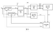
圖1為根據本案一些實施例示出一種時脈資料回復(clock and data recovery,CDR)裝置100的示意圖。CDR裝置100採用類比電路與數位電路之混合控制來調整時脈訊號CKI與時脈訊號CKQ,以提升效能與節省電路面積。FIG. 1 is a schematic diagram showing a clock and data recovery (CDR)
CDR裝置100包含相位偵測電路系統110、類比調變電路系統120、串列轉並行電路130、數位調變電路系統140以及振盪器電路150。於一些實施例中,相位偵測電路系統110根據時脈訊號CKI與時脈訊號CKQ偵測資料訊號SD,以產生上數訊號SUP與下數訊號SDW。於一些實施例中,相位偵測電路系統110可由二元(bang-bang)相位偵測器電路實施。舉例來說,相位偵測電路系統110包含資料取樣電路112、邊緣取樣電路114以及相位偵測器電路116。資料取樣電路112根據時脈訊號CKI對資料訊號SD取樣以產生資料取樣DS。邊緣取樣電路114根據時脈訊號CKQ對資料訊號SD取樣以產生邊緣取樣ES。時脈訊號CKI與時脈訊號CKQ之間的相位差設置為90度。相位偵測器電路116可分析資料取樣DS與邊緣取樣ES之間的相位差,以產生上數訊號SUP與下數訊號SDW。The
類比調變電路系統120根據上數訊號SUP與下數訊號SDW產生調整訊號SA1。於一些實施例中,類比調變電路系統120操作為CDR裝置100中的比例控制(proportional control)路徑。串列轉並行電路130根據上數訊號SUP產生具有M+1位元(即[M:0])的控制訊號BUP,並根據下數訊號SDW產生具有M+1位元的控制訊號BDW,其中M為大於或等於1的正整數。於一些實施例中,串列轉並行電路130用以降低上數訊號SUP以及下數訊號SDW之速度。於一些實施例中,串列轉並行電路130可由解多工器電路實施,但本案並不以此為限。於一些實施例中,若數位調變電路系統140的速度足夠快,上數訊號SUP與下數訊號SDW可直接輸入至數位調變電路系統140(即可不使用串列轉並行電路130)。The analog
數位調變電路系統140根據控制訊號BUP以及控制訊號BDW產生數位碼(如圖2中的數位碼E1),並根據此數位碼產生調整訊號SA2。於一些實施例中,數位調變電路系統140操作為CDR裝置100的積分路徑。振盪器電路150產生時脈訊號CKI與時脈訊號CKQ,並根據調整訊號SA1與調整訊號SA2調整時脈訊號CKI與時脈訊號CKQ。於一些實施例中,如後圖3所示,數位調變電路系統140可包含電流式數位類比轉換器(digital to analog converter,DAC)電路。於此條件下,振盪器電路150為電流控制振盪器電路。於一些實施例中,如後圖4所示,數位調變電路系統140可包含電壓式DAC電路。於此條件下,振盪器電路150為電壓控制振盪器電路。The digital
於一些相關技術中,CDR裝置使用全類比電路實施。於此些技術中,CDR裝置內的迴路濾波器需使用較大容值的電容。如此一來,將耗費較大的電路面積。另外,此電容可能會造成漏電流,使得電路效能降低。於另一些相關技術中,CDR裝置使用全數位電路實施。於此些技術中,由於數位電路之時序延遲,CDR裝置對相位變化之追蹤能力較弱。相較於上述技術,如先前所述,在本案一些實施例中,CDR裝置100採用類比調變電路系統120與數位調變電路系統140之混合控制,其中類比調變電路系統120操作為比例控制路徑且數位調變電路系統140操作為積分路徑。如此一來,CDR裝置100可結合類比電路與數位電路之優點,以在提高效能的同時節省一定的電路面積。In some related technologies, CDR devices are implemented using full analog circuits. In these technologies, the loop filter in the CDR device needs to use a larger capacitance capacitor. As a result, a larger circuit area will be consumed. In addition, this capacitor may cause leakage current, which reduces circuit performance. In other related technologies, CDR devices are implemented using all digital circuits. In these technologies, due to the timing delay of the digital circuit, the CDR device has a weak ability to track phase changes. Compared with the above-mentioned technology, as previously mentioned, in some embodiments of this case, the
圖2為根據本案一些實施例示出圖1的數位調變電路系統140的示意圖。數位調變電路系統140包含決策電路142、濾波器電路144、解碼器電路146以及DAC電路148。決策電路142根據控制訊號BDW與控制訊號BUP產生決策訊號D1。於一些實施例中,決策電路142可由數位訊號處理電路實施。於一些實施例中,決策電路142可比較控制訊號BUP中之預定邏輯值(例如可為邏輯值1)的個數與控制訊號BDW中之預定邏輯值的個數,以產生決策訊號D1。FIG. 2 is a schematic diagram showing the digital
舉例來說,控制訊號BUP的M+1位元中具有3個邏輯值1,且控制訊號BDW的M+1位元中具有1個邏輯值1。於此條件下,控制訊號BUP具有較多的邏輯值1,故決策電路142輸出具有值為1的決策訊號D1,以增加時脈訊號CKI與時脈訊號CKQ之頻率。於一例子中,控制訊號BUP的M+1位元中具有1個邏輯值1,且控制訊號BDW的M+1位元中具有3個邏輯值1。於此條件下,控制訊號BUP具有較少的邏輯值1,故決策電路142輸出具有值為-1的決策訊號D1,以降低時脈訊號CKI與時脈訊號CKQ之頻率。於又一例子中,控制訊號BUP的M+1位元中具有3個邏輯值1,且控制訊號BDW的M+1位元中具有3個邏輯值1。於此條件下,控制訊號BUP與控制訊號BDW具有相同個數的邏輯值1,故決策電路142輸出具有值為0的決策訊號D1,以維持時脈訊號CKI與時脈訊號CKQ之頻率。For example, the M+1 bit of the control signal BUP has three
濾波器電路144對決策訊號D1進行濾波以產生訊號F1。於一些實施例中,濾波器電路144操作為上/下數計數器電路。詳細而言,濾波器電路144在每個週期內對決策訊號D1進行累加。當累加值大於或等於K時,濾波器電路144遞增訊號F1的值。或者,當累加值小於或等於-K時,濾波器電路144遞減訊號F1的值。於一些實施例中,K用於設定濾波器電路144的增益,其中濾波器電路144的增益為1/K。解碼器電路146解碼訊號F1以產生具有N+1位元(即[N:0])的數位碼E1。DAC電路148轉換數位碼E1為調整訊號SA2,其中N可為大於或等於0的整數。The
圖3為根據本案一些實施例示出圖1之類比調變電路系統120與振盪器電路150以及圖2中之DAC電路148的示意圖。於此例中,類比調變電路系統120操作為電荷幫浦(charge pump)電路,其根據上數訊號SUP與下數訊號SDW調整節點N1之位準,以輸出調整訊號SA1。詳細而言,類比調變電路系統120包含電流源I1、電流源I2、開關SW1以及開關SW2。電流源I1耦接於提供電壓VDD的電壓源與開關SW1之間,且電流源I2耦接於開關SW2與提供參考電壓(例如為地電壓GND)的電壓源之間。開關SW1之一端與開關SW2之一端耦接至節點N1。FIG. 3 is a schematic diagram illustrating the analog
若開關SW1根據上數訊號SUP導通,電流源I1之電流(相當於調整訊號SA1)可經由節點N1傳送至振盪器電路150(相當於對節點N1充電)。如此,振盪器電路150可產生頻率較快的時脈訊號CKI與時脈訊號CKQ。或者,若開關SW2根據下數訊號SDW導通,節點N1經由電流源I2放電,以降低流入振盪器電路150之電流(相當於調整訊號SA1)。如此,振盪器電路150可產生頻率較慢的時脈訊號CKI與時脈訊號CKQ。If the switch SW1 is turned on according to the up-count signal SUP, the current of the current source I1 (equivalent to the adjustment signal SA1) can be transmitted to the
DAC電路148為電流式DAC,其包含多個電流源I、…、電流源2N-I。電流源I根據數位碼E1的第1個位元(即E1[0])導通。依此類推,電流源2N-2I根據數位碼E1的第N-1個位元(即E1[N-2])導通。電流源2N-1I根據數位碼E1的第N個位元(即E1[N-1])導通。電流源2NI根據數位碼E1的第N+1個位元(即E1[N])導通。因此,調整訊號SA2即為上述多個電流源中之導通者的電流總和。The
於此例中,振盪器電路150為電流控制振盪器(current controlled oscillator,CCO)電路。於一些實施例中,CCO電路可為由電流鏡電路(未示出)驅動的反相器鏈電路(未示出),其中電流鏡電路可用於複製調整訊號SA1與調整訊號SA2之組合。類比調變電路系統120之輸出耦接至DAC電路148之輸出,以加總調整訊號SA1與調整訊號SA2(於此例中,調整訊號SA1與調整訊號SA2皆為電流訊號)。響應於調整訊號SA1與調整訊號SA2之總和,振盪器電路150可調整時脈訊號CKQ與時脈訊號CKI。例如,當調整訊號SA1與調整訊號SA2之總和越大,時脈訊號CKQ與時脈訊號CKI之頻率越高。或者,當調整訊號SA1與調整訊號SA2之總和越小,時脈訊號CKQ與時脈訊號CKI之頻率越低。In this example, the
圖4為根據本案一些實施例示出圖1之類比調變電路系統120與振盪器電路150以及圖2中之DAC電路148的示意圖。相較於圖3,於此例中,DAC電路148為電壓式DAC電路。例如,DAC電路148可由電阻分壓器(未示出)、多個開關(未示出)以及緩衝器(未示出)實施。多個開關可響應於數位碼E1導通,以使電阻分壓器產生對應於數位碼E1的類比電壓。緩衝器可輸出此類比電壓為調整訊號SA2。上述關於電壓式DAC電路之實施方式用於示例,且本案並不以此為限。各種類型的電壓式DAC電路皆為本案所涵蓋的範圍。4 is a schematic diagram showing the analog
再者,相較於圖3,類比調變電路系統120更包含電阻R。電阻R的一端耦接至節點N1,且電阻R的另一端接收參考電壓VREF(例如可為(但不限於)0.5伏特)。如此,電阻R可將圖3中的調整訊號SA1轉換為電壓訊號。於此例中,振盪器電路150為電壓控制振盪器(voltage controlled oscillator,VCO)電路。於一些實施例中,VCO電路可包含多個電感電容槽(LC tank),以根據調整訊號SA1與調整訊號SA2調整時脈訊號CKQ與時脈訊號CKI。舉例來說,一部分的電感電容槽設定由調整訊號SA1控制,且另一部分的電感電容槽設定由調整訊號SA2控制。如此,振盪器電路150可響應於調整訊號SA1與調整訊號SA2之一組合產生時脈訊號CKI與時脈訊號CKQ。上述關於VCO電路的實施方式用於示例,且本案並不以此為限。Furthermore, compared with FIG. 3, the analog
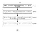
圖5為根據本案一些實施例示出的一種CDR方法500的流程圖。於一些實施例中,CDR方法500可由(但不限於)圖1的CDR裝置100執行。Fig. 5 is a flowchart of a
於操作S510,根據第一時脈訊號與第二時脈訊號偵測資料訊號,以產生上數訊號與下數訊號。In operation S510, the data signal is detected according to the first clock signal and the second clock signal to generate an up signal and a down signal.
於操作S520,藉由類比調變電路系統根據上數訊號與下數訊號產生第一調整訊號。In operation S520, the analog modulation circuit system generates a first adjustment signal according to the up-count signal and the down-count signal.
於操作S530,藉由數位調變電路系統根據第一控制訊號與第二控制訊號產生數位碼,並根據數位碼產生第二調整訊號。In operation S530, the digital modulation circuit system generates a digital code according to the first control signal and the second control signal, and generates a second adjustment signal according to the digital code.
於操作S540,根據第一調整訊號與第二調整訊號產生第一時脈訊號與第二時脈訊號。In operation S540, a first clock signal and a second clock signal are generated according to the first adjustment signal and the second adjustment signal.
上述操作S510、S520、S530以及S540之說明可參照前述各個實施例,故不重複贅述。上述CDR方法500的多個操作僅為示例,並非限定需依照此示例中的順序執行。在不違背本案的各實施例的操作方式與範圍下,在CDR方法500下的各種操作當可適當地增加、替換、省略或以不同順序執行。The description of the foregoing operations S510, S520, S530, and S540 can refer to the foregoing embodiments, so the details are not repeated. The multiple operations of the
綜上所述,本案一些實施例所提供的CDR裝置與CDR方法可使用類比電路與數位電路之混合控制來調整時脈訊號。如此一來,可在提升電路效能的同時節省電路面積。In summary, the CDR device and CDR method provided by some embodiments of the present application can use a hybrid control of an analog circuit and a digital circuit to adjust the clock signal. In this way, circuit area can be saved while improving circuit performance.
雖然本案之實施例如上所述,然而該些實施例並非用來限定本案,本技術領域具有通常知識者可依據本案之明示或隱含之內容對本案之技術特徵施以變化,凡此種變化均可能屬於本案所尋求之專利保護範疇,換言之,本案之專利保護範圍須視本說明書之申請專利範圍所界定者為準。Although the embodiments of this case are as described above, these embodiments are not used to limit the case. Those with ordinary knowledge in the technical field can apply changes to the technical features of the case based on the explicit or implicit content of the case. All may fall into the scope of patent protection sought in this case. In other words, the scope of patent protection in this case shall be subject to the scope of the patent application in this specification.
100:時脈資料回復裝置100: Clock data recovery device
110:相位偵測電路系統110: Phase detection circuit system
112:資料取樣電路112: Data sampling circuit
114:邊緣取樣電路114: edge sampling circuit
116:相位偵測器電路116: Phase detector circuit
120:類比調變電路系統120: Analog modulation circuit system
130:串列轉並行電路130: serial to parallel circuit
140:數位調變電路系統140: Digital Modulation Circuit System
150:振盪器電路150: oscillator circuit
BUP,BDW:控制訊號BUP, BDW: control signal
CKI,CKQ:時脈訊號CKI, CKQ: clock signal
DS:資料取樣DS: Data sampling
ES:邊緣取樣ES: Edge sampling
SA1,SA2:調整訊號SA1, SA2: adjust signal
SD:資料訊號SD: Data signal
SDW:下數訊號SDW: Countdown signal
SUP:上數訊號SUP: Up counting signal
[M:0]:位元[M:0]: bit
Claims (10)
Translated fromChineseApplications Claiming Priority (2)
| Application Number | Priority Date | Filing Date | Title |
|---|---|---|---|
| CN202010145534.9ACN113364452B (en) | 2020-03-05 | 2020-03-05 | Clock data recovery device and clock data recovery method |
| CN202010145534.9 | 2020-03-05 |
Publications (2)
| Publication Number | Publication Date |
|---|---|
| TWI715462Btrue TWI715462B (en) | 2021-01-01 |
| TW202135472A TW202135472A (en) | 2021-09-16 |
Family
ID=75237285
Family Applications (1)
| Application Number | Title | Priority Date | Filing Date |
|---|---|---|---|
| TW109108339ATWI715462B (en) | 2020-03-05 | 2020-03-13 | Clock and data recovery device and clock and data recovery method |
Country Status (3)
| Country | Link |
|---|---|
| US (1) | US11115178B1 (en) |
| CN (1) | CN113364452B (en) |
| TW (1) | TWI715462B (en) |
Families Citing this family (4)
| Publication number | Priority date | Publication date | Assignee | Title |
|---|---|---|---|---|
| CN111010169B (en)* | 2018-10-08 | 2024-01-19 | 中兴通讯股份有限公司 | Phase detection method, device, storage medium and electronic device |
| KR102733872B1 (en)* | 2022-08-26 | 2024-11-26 | 주식회사 실리콘마이터스 | Clock and data recovery device |
| JP7581305B2 (en)* | 2022-11-29 | 2024-11-12 | アンリツ株式会社 | Clock recovery circuit, error rate measurement device, and error rate measurement method |
| US20240322994A1 (en)* | 2023-03-24 | 2024-09-26 | Samsung Electronics Co., Ltd. | System and method of clock and data recovery |
Citations (4)
| Publication number | Priority date | Publication date | Assignee | Title |
|---|---|---|---|---|
| US20110267122A1 (en)* | 2009-01-22 | 2011-11-03 | Glonet Systems, Inc. | All-digital clock data recovery device and transceiver implemented thereof |
| US20150304097A1 (en)* | 2014-04-17 | 2015-10-22 | Global Unichip Corporation | Circuit and method for clock and data recovery |
| TWI535213B (en)* | 2014-10-15 | 2016-05-21 | 創意電子股份有限公司 | Clock and data recovery circuit and method |
| US20180152284A1 (en)* | 2015-07-28 | 2018-05-31 | Rambus Inc. | Collaborative clock and data recovery |
Family Cites Families (10)
| Publication number | Priority date | Publication date | Assignee | Title |
|---|---|---|---|---|
| KR100335442B1 (en)* | 1999-05-26 | 2002-05-04 | 윤종용 | Circuit and method for recovering digital clock |
| TWI229505B (en)* | 2003-12-01 | 2005-03-11 | Via Tech Inc | Data recovery apparatus using a sampling clock with a half frequency of the data rate |
| US20060203939A1 (en)* | 2005-03-11 | 2006-09-14 | Realtek Semiconductor Corporation | Method and apparatus for correcting duty cycle distortion |
| US7692501B2 (en)* | 2007-09-14 | 2010-04-06 | Intel Corporation | Phase/frequency detector and charge pump architecture for referenceless clock and data recovery (CDR) applications |
| JP5365323B2 (en)* | 2009-04-20 | 2013-12-11 | ソニー株式会社 | Clock data recovery circuit and multiplied clock generation circuit |
| US8284888B2 (en)* | 2010-01-14 | 2012-10-09 | Ian Kyles | Frequency and phase acquisition of a clock and data recovery circuit without an external reference clock |
| US8804888B2 (en)* | 2010-07-12 | 2014-08-12 | Ensphere Solutions, Inc. | Wide band clock data recovery |
| CN109450439B (en)* | 2015-04-23 | 2022-06-07 | 群联电子股份有限公司 | Clock data recovery circuit module, memory storage device and phase locking method |
| CN108282162B (en)* | 2017-01-06 | 2021-08-31 | 联咏科技股份有限公司 | Clock and Data Recovery Circuits with Improved Jitter Tolerance |
| US11212074B2 (en)* | 2017-09-11 | 2021-12-28 | Sony Semiconductor Solutions Corporation | Data reception device and data transmission/reception device |
- 2020
- 2020-03-05CNCN202010145534.9Apatent/CN113364452B/enactiveActive
- 2020-03-13TWTW109108339Apatent/TWI715462B/enactive
- 2020-11-17USUS17/099,819patent/US11115178B1/enactiveActive
Patent Citations (4)
| Publication number | Priority date | Publication date | Assignee | Title |
|---|---|---|---|---|
| US20110267122A1 (en)* | 2009-01-22 | 2011-11-03 | Glonet Systems, Inc. | All-digital clock data recovery device and transceiver implemented thereof |
| US20150304097A1 (en)* | 2014-04-17 | 2015-10-22 | Global Unichip Corporation | Circuit and method for clock and data recovery |
| TWI535213B (en)* | 2014-10-15 | 2016-05-21 | 創意電子股份有限公司 | Clock and data recovery circuit and method |
| US20180152284A1 (en)* | 2015-07-28 | 2018-05-31 | Rambus Inc. | Collaborative clock and data recovery |
Also Published As
| Publication number | Publication date |
|---|---|
| US11115178B1 (en) | 2021-09-07 |
| CN113364452A (en) | 2021-09-07 |
| US20210281389A1 (en) | 2021-09-09 |
| TW202135472A (en) | 2021-09-16 |
| CN113364452B (en) | 2024-07-12 |
Similar Documents
| Publication | Publication Date | Title |
|---|---|---|
| TWI715462B (en) | Clock and data recovery device and clock and data recovery method | |
| US8373460B2 (en) | Dual loop phase locked loop with low voltage-controlled oscillator gain | |
| US7330058B2 (en) | Clock and data recovery circuit and method thereof | |
| US8063678B2 (en) | Charge pump for phase locked loop | |
| US20020050864A1 (en) | Low offset and low glitch energy charge pump for PLL-based timing recovery systems | |
| CN103297042A (en) | Charge pump phase-locked loop circuit capable of being locked quickly | |
| US20080303569A1 (en) | Delay locked loop circuit | |
| CN105071799A (en) | Delay-locked loop adopting novel error lock detection circuit | |
| CN106603070B (en) | Low-stray fast-locking phase-locked loop circuit | |
| US11736113B2 (en) | Automatic hybrid oscillator gain adjustor circuit | |
| US6646512B2 (en) | Self-bias and differential structure based PLL with fast lockup circuit and current range calibration for process variation | |
| US6157691A (en) | Fully integrated phase-locked loop with resistor-less loop filer | |
| US6472914B2 (en) | Process independent ultralow charge pump | |
| CN108988853B (en) | Digital auxiliary locking circuit | |
| US6853254B2 (en) | Anti-deadlock circuit and method for phase-locked loops | |
| US7375557B2 (en) | Phase-locked loop and method thereof and a phase-frequency detector and method thereof | |
| CN106209079A (en) | A kind of phase-locked loop circuit reducing the loop-locking time | |
| CN101931401A (en) | Phase detection discriminator and charge pump combined circuit structure applied to phase-locked loop | |
| US7236025B2 (en) | PLL circuit and program for same | |
| US8368443B1 (en) | Differential charge pump circuit | |
| US6717446B1 (en) | High speed programmable charge-pump with low charge injection | |
| US9391626B2 (en) | Capacitive load PLL with calibration loop | |
| CN111147071A (en) | A Proportional Path Gain Regulator Applied in Clock-Data Recovery Circuit | |
| CN117294138A (en) | Charge pump with output current regulation | |
| CN117879593B (en) | A phase-locked loop circuit with anti-interference function and corresponding electronic equipment |