Movatterモバイル変換


[0]ホーム

URL:


TWI714553B - Auto capacitance tuner current compensation to control one or more film properties through target life - Google Patents

Auto capacitance tuner current compensation to control one or more film properties through target life
Download PDF

Info

Publication number
TWI714553B
TWI714553BTW105105300ATW105105300ATWI714553BTW I714553 BTWI714553 BTW I714553BTW 105105300 ATW105105300 ATW 105105300ATW 105105300 ATW105105300 ATW 105105300ATW I714553 BTWI714553 BTW I714553B
Authority
TW
Taiwan
Prior art keywords
target
substrate
automatic capacitance
set point
automatic
Prior art date
Application number
TW105105300A
Other languages
Chinese (zh)
Other versions
TW201636446A (en
Inventor
葛振斌
古普塔維菲克
艾倫阿道夫米勒
韓森萊恩
Original Assignee
美商應用材料股份有限公司
Priority date (The priority date is an assumption and is not a legal conclusion. Google has not performed a legal analysis and makes no representation as to the accuracy of the date listed.)
Filing date
Publication date
Application filed by 美商應用材料股份有限公司filedCritical美商應用材料股份有限公司
Publication of TW201636446ApublicationCriticalpatent/TW201636446A/en
Application grantedgrantedCritical
Publication of TWI714553BpublicationCriticalpatent/TWI714553B/en

Links

Images

Classifications

Landscapes

Abstract

In some embodiments a method of depositing a metal-containing layer atop a substrate disposed in a physical vapor deposition (PVD) chamber includes: providing a plasma forming gas to a processing region of the PVD chamber; providing a first amount of RF power to a target assembly disposed opposite the substrate to form a plasma within the processing region of the PVD chamber; sputtering source material from the target assembly to deposit a metal-containing layer onto the substrate, wherein the source material is at a first erosion state; and tuning an auto capacitance tuner coupled to a substrate support while sputtering source material to maintain an ion energy at a surface of the substrate within a predetermined range as the target erodes from the first erosion state to a second erosion state.

Description

Translated fromChinese
透過靶壽命控制一或多個薄膜性質的自動電容調節器電流補償Automatic capacitance regulator current that controls one or more film properties through target lifemake up

本發明揭露的實施例一般係關於基板處理系統。The disclosed embodiments of the present invention generally relate to substrate processing systems.

用在後段(BEOL)硬遮罩應用的高密度、低應力薄膜(如氮化鈦(TiN)膜)用於減少用在圖案化低介電常數的介電(low-k dielectric)溝槽之線彎曲以及藉由降低線邊緣粗糙度和臨界尺寸(CD)變化來改善低k蝕刻剖面。The high-density, low-stress film (such as titanium nitride (TiN) film) used in the back-end (BEOL) hard mask application is used to reduce the pattern of low-k dielectric trenches. Line bending and improved low-k etch profile by reducing line edge roughness and critical dimension (CD) variation.

射頻(RF)功率可提供至主要DC電漿以增加電漿中濺射材料的離子化率。增加的離子化率允許改善到達原子的表面流動性,而導致結晶膜定向,其有利於產生低應力且緻密薄膜。此外,到達基板水平面(level)的高比例離子化材料允許藉由晶圓基座阻抗電路的裝置調節輸入的離子能。Radio frequency (RF) power can be provided to the main DC plasma to increase the ionization rate of sputtered materials in the plasma. The increased ionization rate allows to improve the surface fluidity to the atoms, leading to the orientation of the crystalline film, which is beneficial to produce a low-stress and dense film. In addition, the high proportion of ionized material reaching the level of the substrate allows the input ion energy to be adjusted by the device of the wafer base impedance circuit.

RF功率平行供應於腔室陰極處(即濺射靶)。磁控管用於增加靶表面處的電子約束以改善電漿穩定性和濺射速率。侵蝕軌道建立於材料被優先濺射所在的靶表面上。The RF power is supplied parallel to the cathode of the chamber (ie, the sputtering target). The magnetron is used to increase the electron confinement at the target surface to improve the plasmaStability and sputtering rate. The erosion trajectory is established on the surface of the target where the material is preferentially sputtered.

使用供應RF功率給靶並結合靶表面處磁性約束的一個缺點是:當靶材料被侵蝕時,RF功率傳輸的效率降低。當靶材料因為以下原因被侵蝕時,而RF功率傳輸的效率降低:隨著靶變薄,磁鐵表面到靶的濺射表面之物理距離減少。此外,靶表面上的侵蝕軌道進一步降低了RF功率輸送的效率,而侵蝕軌道可進一步限制電子並因此降低在基板水平處的電漿密度。隨著磁性約束增大,RF電流供應的電子無法像遵循增強(為侵蝕深度的函數)磁場線那樣有效地傳播進入電漿。One disadvantage of using the supply of RF power to the target combined with the magnetic confinement at the target surface is that when the target material is eroded, the efficiency of RF power transmission is reduced. When the target material is eroded due to the following reasons, the efficiency of RF power transmission decreases: As the target becomes thinner, the physical distance from the magnet surface to the sputtering surface of the target decreases. In addition, the eroded trajectory on the target surface further reduces the efficiency of RF power delivery, and the eroded trajectory can further confine the electrons and thus reduce the plasma density at the substrate level. As the magnetic confinement increases, the electrons supplied by the RF current cannot propagate into the plasma as efficiently as following the enhanced (as a function of erosion depth) magnetic field lines.

傳送到電漿的RF功率之減少降低了離子化率,離子化率的減少直接見於基板支撐件阻抗電路處所測量的電流之減少以及間接見於薄膜性質上的影響。由於磁性約束的增加,與更高離子化相關之有利的薄膜性質(如低應力與高密度)開始以靶壽命(target life)的函數退化。The reduction of the RF power delivered to the plasma reduces the ionization rate. The reduction of the ionization rate is directly seen in the reduction of the current measured at the impedance circuit of the substrate support and indirectly seen in the effect of the film properties. As the magnetic confinement increases, the favorable film properties associated with higher ionization (such as low stress and high density) begin to degrade as a function of target life.

因此,本發明人已提供了一種用於處理基板的改進方法和設備。Therefore, the inventors have provided an improved method and apparatus for processing substrates.

本發明揭露的實施例包括用於處理基板的方法與設備。在一些實施例中,一種將含金屬層沉積於設置在物理氣相沉積(PVD)腔室中的基板上之方法,包括以下步驟:提供電漿形成氣體給該PVD腔室的處理區域;提供第一量的RF功率給相對於該基板設置的靶組件以在該PVD腔室的該處理區域內形成電漿;將來自該靶組件的源材料濺射以將含金屬層沉積於該基板上,其中該源材料是在第一侵蝕狀態;及當該靶從該第一侵蝕狀態侵蝕至第二侵蝕狀態,濺射源材料以維持該基板的表面處之離子能在一預定範圍內的同時,調節與基板支撐件耦接的自動電容調節器。The disclosed embodiments of the present invention include methods and equipment for processing substrates. In some embodiments, a method for depositing a metal-containing layer on a substrate provided in a physical vapor deposition (PVD) chamber includes the following steps: providing a plasma forming gas to the processing area of the PVD chamberProvide a first amount of RF power to the target assembly set relative to the substrate to form plasma in the processing area of the PVD chamber; sputter the source material from the target assembly to deposit a metal-containing layer on On the substrate, wherein the source material is in a first erosion state; and when the target is eroded from the first erosion state to the second erosion state, the source material is sputtered to maintain the ion energy at the surface of the substrate in a predetermined range At the same time, adjust the automatic capacitance adjuster coupled with the substrate support.

在一些實施例中,一種將含金屬層沉積於設置在物理氣相沉積(PVD)腔室中的基板上之方法,包括以下步驟:提供電漿形成氣體給該PVD腔室的處理區域;提供第一量的RF功率給相對於該基板設置的靶組件以在該PVD腔室的該處理區域內形成電漿;將來自該靶組件的源材料濺射以將含金屬層沉積於該基板上,其中該源材料在第一侵蝕狀態是實質上未侵蝕的;及當該靶從該第一侵蝕狀態侵蝕至第二侵蝕狀態,濺射源材料以維持該基板的表面處之離子能在一預定範圍內的同時,調節與基板支撐件耦接的自動電容調節器,其中該源材料在該第二侵蝕狀態是實質上已侵蝕的。In some embodiments, a method for depositing a metal-containing layer on a substrate disposed in a physical vapor deposition (PVD) chamber includes the following steps: providing plasma forming gas to the processing area of the PVD chamber; providing A first amount of RF power is applied to a target assembly disposed relative to the substrate to form plasma in the processing area of the PVD chamber; source material from the target assembly is sputtered to deposit a metal-containing layer on the substrate , Wherein the source material is substantially uneroded in the first erosion state; and when the target is eroded from the first erosion state to the second erosion state, the source material is sputtered to maintain the ion energy at the surface of the substrate While adjusting within a predetermined range, the automatic capacitance adjuster coupled with the substrate support is adjusted, wherein the source material is substantially eroded in the second erosion state.

在一些實施例中,提供一種電腦可讀取媒體,具有儲存於其上之指令,當執行該等指令時,導致物理氣相沉積(PVD)腔室執行一種將含金屬層沉積於基板上之方法。該方法可包括本發明所揭露實施例中的任一者。In some embodiments, a computer-readable medium is provided with instructions stored thereon. When the instructions are executed, a physical vapor deposition (PVD) chamber executes a method of depositing a metal-containing layer on a substrate. method. The method may include any of the embodiments disclosed in the present invention.

本說明書揭露的其他和進一步的實施例描述如下。Other and further embodiments disclosed in this specification are described below.

100:PVD處理腔室100: PVD processing chamber

102:腔室蓋102: chamber cover

103:接地組件103: Grounding component

104:處理腔室104: processing chamber

106:基板支撐件106: substrate support

108:基板108: substrate

110:下部接地外殼壁110: Lower grounding shell wall

112:接地屏蔽112: Ground shield

114:靶組件114: target assembly

116:上部接地外殼壁116: upper grounding shell wall

118:中央處理單元(CPU)118: Central Processing Unit (CPU)

120:處理區域120: Processing area

122:波紋管122: bellows

124:底部腔室壁124: bottom chamber wall

126:氣體源126: Gas source

128:質量流量控制器128: Mass flow controller

130:排氣口130: exhaust port

132:閥132: Valve

134:RF偏壓電源134: RF bias power supply

136:自動電容調節器136: automatic capacitance regulator

138:屏蔽138: Shield

140:突出部分140: protruding part

146:蓋環146: cover ring

148:可旋轉磁體組件148: Rotatable magnet assembly

150:複數個磁體150: multiple magnets

152:磁體152: Magnet

154:電極154: Electrode

156:接地板156: Ground Plate

157:第一表面157: First Surface

158:源分配板158: Source Distribution Board

160:背板組件160: Backplane components

161:第一背板161: First Backplane

162:第二背板162: second backplane

164:導電支撐環164: Conductive support ring

166:第一端166: first end

168:第二端168: second end

169:通道169: Channel

170:腔體170: Cavity

172:記憶體172: Memory

173:支援電路173: Support Circuit

174:馬達軸174: Motor shaft

175:支撐構件175: Support member

176:馬達176: Motor

178:齒輪組件178: Gear assembly

180:絕緣間隙180: insulation gap

181:密封環181: Seal ring

182:RF電源182: RF power supply

183:第二能量源183: Second Energy Source

186:中心軸186: Central axis

192:中心支撐構件192: Central support member

194:控制器194: Controller

200:方法200: method

202:步驟202: Step

204:步驟204: Step

206:步驟206: Step

208:步驟208: Step

本發明揭露之實施例已簡要概述於前,並在以下有更詳盡之討論,可以藉由參考所附圖式中繪示之本發明實施例以作瞭解。然而,值得注意的是,所附圖式只繪示了本發明揭露的典型實施例,而由於本發明可允許其他等效之實施例,所附圖式並不會視為本發明範圍之限制。The disclosed embodiments of the present invention have been briefly summarized above, and will be discussed in more detail below, which can be understood by referring to the embodiments of the present invention shown in the accompanying drawings. However, it is worth noting that the attached drawings only show typical embodiments disclosed in the present invention, and since the present invention may allow other equivalent embodiments, the attached drawings are not considered to limit the scope of the present invention .

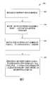
圖1繪示根據本發明揭露的一些實施例之處理腔室的概要截面圖。FIG. 1 is a schematic cross-sectional view of a processing chamber according to some embodiments disclosed in the present invention.

圖2繪示根據本發明揭露的一些實施例之處理基板的方法之流程圖。FIG. 2 shows a flowchart of a method of processing a substrate according to some embodiments disclosed in the present invention.

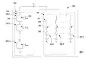
圖3繪示根據本發明揭露的一些實施例之自動電容調節器的電路實施。FIG. 3 shows a circuit implementation of an automatic capacitance regulator according to some embodiments disclosed in the present invention.

圖4繪示根據本發明揭露的一些實施例之示例性自動電容調節器的共振曲線(resonance curve)。FIG. 4 illustrates a resonance curve of an exemplary automatic capacitance adjuster according to some embodiments disclosed in the present invention.

為便於理解,在可能的情況下,使用相同的數字編號代表圖示中相同的元件。該等圖示未依比例繪示,且可為求清楚而簡化。一個實施例的元件與特徵可有利地用於其它實施例中而無需贅述。For ease of understanding, where possible, the same numbers are used to represent the same elements in the drawings. The illustrations are not drawn to scale and may be simplified for clarity. The elements and features of one embodiment can be advantageously used in other embodiments without repeating them.

本發明係關於一種處理基板的方法。在一些實施例中,本發明揭露係關於將含金屬層沉積於設置在物理氣相沉積(PVD)腔室中的基板上之方法。在一些實施例中,本文描述的發明方法有利地促進含金屬層的沉積適宜作為硬遮罩層,例如氮化鈦層,具有改進的應力,電阻率和密度均勻的特性。例如,用在後段(BEOL)硬遮罩應用的高密度、低應力氮化鈦(TiN)膜或類似物用來減少用在圖案化低介電常數的介電(low-k dielectric)溝槽之線彎曲以及藉由減少線邊緣粗糙度和臨界尺寸(CD)變化來改善低k蝕刻剖面。The present invention relates to a method of processing a substrate. In some embodiments, the present invention discloses a method for depositing a metal-containing layer on a substrate provided in a physical vapor deposition (PVD) chamber. In some embodiments, the inventive method described herein advantageously promotes the deposition of a metal-containing layer suitable as a hard mask layer, such as a titanium nitride layer, with improved stress, uniform resistivity and density characteristics. For example, high-density, low-stress titanium nitride (TiN) films or the like used in back-end (BEOL) hard mask applications are used to reduce the patterning of low-k dielectric trenches. The line bending and the improvement of low-k etching profile by reducing line edge roughness and critical dimension (CD) variation.

圖1繪示根據本發明揭露的一些實施例之物理氣相沉積(PVD)處理腔室100的簡化截面圖。圖2繪示將層沉積於基板上之方法200的流程圖,基板設置在圖1所述類型的物理氣相沉積處理系統中。適合用於執行本發明所述的方法200的其他PVD腔室之示範例包括可自美國加州聖克拉拉的應用材料公司購得的CIRRUSTM與AVENIRTM PVD處理腔室。FIG. 1 shows a simplified cross-sectional view of a physical vapor deposition (PVD)processing chamber 100 according to some embodiments disclosed in the present invention. FIG. 2 shows a flow chart of amethod 200 of depositing a layer on a substrate. The substrate is set in a physical vapor deposition processing system of the type described in FIG. 1. Examples of other PVD chambers suitable for performing themethod 200 of the present invention include CIRRUS and AVENIR PVD processing chambers available from Applied Materials, Inc. of Santa Clara, California.

該方法200執行於處理腔室內的基板108上,例如在圖1所示的物理氣相沉積(PVD)處理腔室(處理腔室104)。圖1所示的處理腔室104包括基板支撐件106、靶組件114及源材料113,靶組件114具有可選的背板組件160,源材料113設置於面向背板組件160側的基板支撐件上。處理腔室104進一步包括射頻(RF)功率源182以提供RF能到靶組件114。Themethod 200 is executed on asubstrate 108 in a processing chamber, such as a physical vapor deposition (PVD) processing chamber (processing chamber 104) shown in FIG. 1. Theprocessing chamber 104 shown in FIG. 1 includes asubstrate support 106, atarget assembly 114, and asource material 113. Thetarget assembly 114 has an optionalback plate assembly 160. Thesource material 113 is disposed on the substrate support on the side facing theback plate assembly 160. on. Theprocessing chamber 104 further includes a radio frequency (RF)power source 182 to provide RF energy to thetarget assembly 114.

基板108可以是具有任何合適的幾何形狀之任何合適的基板,如圓形晶圓、方形、矩形或類似物。基板108可包括任何合適的材料,如矽(Si)、氧化矽(SiO2)、氮化矽(SiN)、玻璃、其他介電材料或類似物中的一或多個,且可具有設置於基板108之上的其它材料中的一或多個層。在一些實施例中,基板108可包括低k介電材料的上層,且在一些實施例中,可包括超低k電介質材料(ultra-low k dielectric material)。如本發明所用的超低k介電材料包括具有小於或等於約2.5的k值之介電材料。基板108可係空白(blank)基板(如於其上不具有特徵),或基板108可具有形成於基板中或基板上的特徵,如通孔或溝槽,或高深寬比的特徵,例如,針對通過矽通孔(TSV)的應用或類似物。本說明書所用的高寬比特徵可包括具有至少約5:1的高度比寬度的深寬比之特徵。Thesubstrate 108 may be any suitable substrate having any suitable geometric shape, such as a round wafer, a square, a rectangle, or the like. Thesubstrate 108 may include any suitable material, such as one or more of silicon (Si), silicon oxide (SiO2 ), silicon nitride (SiN), glass, other dielectric materials, or the like, and may have One or more layers of other materials above thesubstrate 108. In some embodiments, thesubstrate 108 may include an upper layer of a low-k dielectric material, and in some embodiments, may include an ultra-low k dielectric material. The ultra-low-k dielectric material used in the present invention includes a dielectric material having a k value less than or equal to about 2.5. Thesubstrate 108 may be a blank substrate (if there are no features thereon), or thesubstrate 108 may have features formed in or on the substrate, such as vias or trenches, or features with high aspect ratio, for example, For through silicon vias (TSV) applications or similar. The aspect ratio feature used in this specification may include a feature having an aspect ratio of at least about 5:1 height to width.

方法200開始於202,其中提供電漿形成氣體給處理腔室104的處理區域120。電漿形成氣體可包括一或多個惰性氣體,如稀有氣體或其它惰性氣體。例如,電漿形成氣體之非限制性示範例包括氬(Ar)、氦(He)、氙(Xe)、氖(Ne)、氫(H2)、氮(N2)、氧(O2)等中的一或多種。Themethod 200 starts at 202 where a plasma forming gas is provided to theprocessing area 120 of theprocessing chamber 104. The plasma forming gas may include one or more inert gases, such as rare gases or other inert gases. For example, non-limiting examples of plasma forming gases include argon (Ar), helium (He), xenon (Xe), neon (Ne), hydrogen (H2 ), nitrogen (N2 ), oxygen (O2 ) One or more of etc.

在204處,提供第一量的RF功率給靶組件114以在PVD腔室104的處理區域120內引燃電漿形成氣體而成為電漿。RF功率是於處理區域120內形成電漿之適合的量之RF功率,其可根據腔室尺寸、幾何形狀或類似物而改變。例如,在一些實施例中,第一量的RF功率是約500至約20000瓦。在一些實施例中,提供給靶組件的RF功率之量可以在整個靶的壽命中保持恆定。在一些實施例中,RF功率之量可以隨著靶的壽命增加,以補償隨著靶侵蝕時電漿內減少的離子化率。At 204, a first amount of RF power is provided to thetarget assembly 114 to ignite the plasma in theprocessing area 120 of thePVD chamber 104 to form a gas to become plasma. RF power is to form plasma in theprocessing area 120The suitable amount of RF power can be changed according to the chamber size, geometry or the like. For example, in some embodiments, the first amount of RF power is about 500 to about 20,000 watts. In some embodiments, the amount of RF power provided to the target assembly can remain constant throughout the life of the target. In some embodiments, the amount of RF power may increase with the lifetime of the target to compensate for the reduced ionization rate in the plasma as the target erodes.

在206處,源材料113從靶組件114濺射以將含金屬層沉積於基板108上。當源材料113開始濺射時,源材料113在第一侵蝕狀態。在一些實施例中,源材料113在第一侵蝕狀態實質上是未侵蝕的(即處於或非常接近靶壽命的開始)。源材料113可包括適於在基板108上形成含有金屬的層之金屬、金屬合金或類似物中的一或多種。例如,該源材料113可包括鈦(Ti)、鉭(Ta)、銅(Cu)、鈷(Co)、鎢(W)或鋁(Al)或類似物中的一或多個。當使用電漿濺射來自源材料113的金屬原子時,於處理腔室104中保持在第一壓力。第一壓力係足以將自靶組件114濺射的金屬原子之主要部分離子化的壓力。第一壓力可取決於處理腔室的幾何形狀(如基板尺寸、靶到基板的距離等)。At 206, thesource material 113 is sputtered from thetarget assembly 114 to deposit the metal-containing layer on thesubstrate 108. When the source material 113 starts to sputter, thesource material 113 is in the first erosion state. In some embodiments, thesource material 113 is substantially uneroded in the first eroded state (ie, at or very close to the beginning of the target lifetime). Thesource material 113 may include one or more of metals, metal alloys, or the like suitable for forming a metal-containing layer on thesubstrate 108. For example, thesource material 113 may include one or more of titanium (Ti), tantalum (Ta), copper (Cu), cobalt (Co), tungsten (W), aluminum (Al), or the like. When plasma is used to sputter the metal atoms from thesource material 113, the first pressure is maintained in theprocessing chamber 104. The first pressure is a pressure sufficient to ionize the main part of the metal atoms sputtered from thetarget assembly 114. The first pressure may depend on the geometry of the processing chamber (such as the size of the substrate, the distance from the target to the substrate, etc.).

當沉積含金屬層(如氮化鈦層)時,發明人已經觀察到,藉由施加RF功率於靶組件114增加了電漿內的氮和鈦的離子化率而允許改善到達原子的表面流動性,因而提供結晶膜定向,其有利於產生低應力且緻密薄膜。此外,到達基板108水平面的高比例離子化材料允許使用基板支撐件阻抗電路(如以下相對於圖1與3所述的自動電容調節器136)來調節輸入的離子能(即在基板表面處的離子能),以控制基板電流(如在基板水平面處的離子能)而進一步利於控制結晶膜定向,其有利於形成低應力且緻密薄膜。自動電容調節器136調整自基板支撐基座電極至接地的電容(以及阻抗)。示例性基板支撐阻抗電路(如自動電容調節器136)可提供約0.5至約20安培的電流。除了在靶壽命中維持期望的薄膜性質,本發明人進一步觀察到,當使用根據本發明揭露的方法時,可用的靶壽命可以有利地從約1000kWh增加到約4000kWh。When depositing a metal-containing layer (such as a titanium nitride layer), the inventors have observed that by applying RF power to thetarget assembly 114, the ionization rate of nitrogen and titanium in the plasma is increased and the surface flow to atoms is improved. This provides crystalline film orientation, which facilitates the production of low-stress and dense films. In addition, the high proportion of ionized materials reaching the level of thesubstrate 108Allows the use of the substrate support impedance circuit (such as theautomatic capacitance adjuster 136 described below with respect to Figures 1 and 3) to adjust the input ion energy (that is, the ion energy at the substrate surface) to control the substrate current (such as the substrate current The ion energy at the horizontal plane is further conducive to controlling the orientation of the crystalline film, which is conducive to the formation of a low-stress and dense film. Theautomatic capacitance adjuster 136 adjusts the capacitance (and impedance) from the substrate supporting base electrode to the ground. An exemplary substrate supporting impedance circuit (such as the automatic capacitance adjuster 136) can provide a current of about 0.5 to about 20 amperes. In addition to maintaining the desired film properties during the target lifetime, the inventors further observed that when using the method disclosed according to the present invention, the usable target lifetime can be advantageously increased from about 1000 kWh to about 4000 kWh.

然而,本發明人還觀察到,隨著靶材料侵蝕,施加到靶組件114的RF功率之效率降低,導致電漿中的離子密度減少。雖然可以增加RF功率的量以補償降低的靶壽命中之離子化率,但是發明人觀察到只有這種補償是不足以維持在靶壽命中一致的沉積薄膜性質。不希望受理論的限制,發明人相信在RF功率的效率之降低是因為當靶變薄時,從磁體表面到靶的濺射表面之物理距離的減小。此外,來自濺射處理在源材料113表面上形成的侵蝕軌道限制了電子並因此降低在基板水平處的電漿密度。隨著磁性約束增大,RF電流供應的電子無法像遵循(follow)增強(為侵蝕深度的函數)磁場線那樣有效地傳播進入電漿。本發明人還發現通過在靶壽命的過程中控制離子能並提供離子能(如電流)補償以在基板水平面處提供受控增加量的離子能以補償減少的離子密度,而有利地達到改善薄膜性質的控制。However, the inventors have also observed that as the target material erodes, the efficiency of the RF power applied to thetarget assembly 114 decreases, resulting in a decrease in the ion density in the plasma. Although the amount of RF power can be increased to compensate for the reduced ionization rate during the target lifetime, the inventors have observed that this compensation alone is not sufficient to maintain consistent deposited film properties over the target lifetime. Without wishing to be bound by theory, the inventor believes that the reduction in the efficiency of RF power is due to the decrease in the physical distance from the magnet surface to the sputtering surface of the target when the target becomes thinner. In addition, the erosion trajectory formed on the surface of the source material 113 from the sputtering process limits electrons and thus reduces the plasma density at the substrate level. As the magnetic confinement increases, the electrons supplied by the RF current cannot propagate into the plasma as efficiently as following the enhanced (as a function of erosion depth) magnetic field lines. The inventors also found that by controlling the ion energy and providing ion energy (such as current) compensation during the life of the target, the substrateA controlled increasing amount of ion energy is provided at the horizontal level to compensate for the reduced ion density, which advantageously achieves the control of improving the film properties.

PVD處理系統100進一步包括基板支撐阻抗電路(如自動電容調節器136),其耦接至基板支撐件106以用於在基板108處調整電漿鞘(plasma sheath)電壓。例如,在自動電容調節器136可用於控制基板108處的鞘電壓,以及因此控制基板電流(例如,在基板水平面處的離子能)。因此,在208,當濺射源材料113時,自動電容調節器136經調諧而將在基板支撐件處的RF電流之量維持在一預定的設定點值或維持於預定的設定點值的一個預定範圍內。ThePVD processing system 100 further includes a substrate supporting impedance circuit (such as an automatic capacitance adjuster 136), which is coupled to thesubstrate support 106 for adjusting the plasma sheath voltage at thesubstrate 108. For example, theautomatic capacitance adjuster 136 can be used to control the sheath voltage at thesubstrate 108, and therefore the substrate current (eg, ion energy at the level of the substrate). Therefore, at 208, when thesource material 113 is sputtered, theautomatic capacitance adjuster 136 is tuned to maintain the amount of RF current at the substrate support at a predetermined set point value or at one of the predetermined set point values. Within the predetermined range.

在一些實施例中,調整自動電容調節器136包括計算預定的設定點值及計算預定的設定點位置。預定的設定點位置可根據經驗決定或通過將自動電容調節器136位置與最高電流輸出建模(modeling)來決定。In some embodiments, adjusting theautomatic capacitance adjuster 136 includes calculating a predetermined set point value and calculating a predetermined set point position. The predetermined set point position can be determined empirically or by modeling the position of theautomatic capacitance adjuster 136 with the highest current output.

計算預定的設定點值以當源材料113侵蝕時(即從第一侵蝕狀態到第二侵蝕狀態),在基板的表面處維持實質恆定的離子能。如本文所用的術語「實質恆定的離子能」指的是將離子能維持於第一侵蝕狀態離子能的20%以內,或維持於第一侵蝕狀態離子能的10%以內。在一些實施例中,可計算預定的設定點值將基板表面處的離子能維持於靶在第一侵蝕狀態時基板表面處的離子能之約10%至20%之間。例如,可藉由決定預定義的基於靶壽命的補償係數(「係數」)來計算預定的設定點值。該係數可根據經驗決定或藉由基於靶壽命的建模來決定,以當源材料113在第二侵蝕狀態時(如相較第一侵蝕狀態有更多的侵蝕)維持基板表面處的一恆定離子能。該係數是為了維持從靶壽命開始到靶壽命結束的等效薄膜性質所需的從靶壽命開始到靶壽命結束之電流差除以所用的靶壽命之百分比。該係數可儲存於控制器194中,如下所述且描繪於圖1中。在一些實施例中,源材料113在第二侵蝕狀態是實質上已侵蝕的(即處於靶壽命結束或很接近靶壽命結束)。在一些實施例中,源材料113在第一侵蝕狀態實質上是未侵蝕的(即未使用或準備開始處理基板),而源材料113在第二侵蝕狀態是實質上已侵蝕的(即處於靶壽命結束或很接近靶壽命結束)。A predetermined set point value is calculated to maintain a substantially constant ion energy at the surface of the substrate when thesource material 113 is eroded (ie, from the first erosion state to the second erosion state). The term "substantially constant ion energy" as used herein refers to maintaining the ion energy within 20% of the ion energy in the first erosion state, or within 10% of the ion energy in the first erosion state. In some embodiments, a predetermined set point value can be calculated to maintain the ion energy at the substrate surface at about 10% to 20% of the ion energy at the substrate surface when the target is in the first erosion state. For example, by determining a predefined compensation coefficient ("coefficient") based on the life of the target, the predetermined setting can be calculated.Fixed-point value. The coefficient can be determined empirically or by modeling based on the target lifetime, so that when thesource material 113 is in the second erosion state (for example, there is more erosion than the first erosion state) to maintain a constant at the substrate surface Ion energy. This coefficient is the percentage of the current difference from the beginning of the target life to the end of the target life required to maintain the equivalent film properties from the beginning of the target life to the end of the target life divided by the target life used. This coefficient may be stored in thecontroller 194, as described below and depicted in FIG. 1. In some embodiments, thesource material 113 is substantially eroded in the second erosion state (ie, at the end of the target life or very close to the end of the target life). In some embodiments, thesource material 113 in the first eroded state is substantially uneroded (i.e. unused or ready to process the substrate), and thesource material 113 in the second eroded state is substantially eroded (i.e. in the target End of life or very close to the end of target life).

因此,在一些實施例中,跨自動電容調節器136的電流可經測量以測定基板處的離子能,以及如果需要回應測得的電流而為了維持基板處的離子能在上述所需的程度,可以調整自動電容調節器136的位置或設定點。可替代地或組合地,可以測量基板上的偏壓(且將其與基板處的離子能根據經驗相關聯(correlate)或藉由建模相關聯)並用此偏壓來決定實際的離子能是否需要增加或減少(並調整自動電容調節器136)以將基板處的離子能維持於所需的程度。Therefore, in some embodiments, the current across theautomatic capacitance adjuster 136 can be measured to determine the ion energy at the substrate, and if necessary, in response to the measured current, in order to maintain the ion energy at the substrate to the above required level, The position or set point of theautomatic capacitance adjuster 136 can be adjusted. Alternatively or in combination, the bias voltage on the substrate can be measured (and correlated with the ion energy at the substrate based on experience or by modeling) and used this bias to determine whether the actual ion energy It is necessary to increase or decrease (and adjust the automatic capacitance adjuster 136) to maintain the ion energy at the substrate to the desired level.

在一些實施例中,調整自動電容調節器136包括將自動電容調節器136的位置與預定的設定點位置比較。在一些實施例中,自動電容調節器136的位置大於(greater)預定的設定點位置,而自動電容調節器136控制的RF功率之量(如藉由來自自動電容調節器136的電流所測得的基板水平面處的離子電流)小於預定的設定點值。在此實施例中,減少自動電容調節器136的位置直到自動電容調節器136所控制的RF功率之量(在自動電容調節器136測量的電流)等於預定的設定點值。In some embodiments, adjusting theautomatic capacitance adjuster 136 includes adjusting the position of theautomatic capacitance adjuster 136 to a predetermined set point position.Compare. In some embodiments, the position of theautomatic capacitance adjuster 136 is greater than the predetermined set point position, and the amount of RF power controlled by the automatic capacitance adjuster 136 (as measured by the current from theautomatic capacitance adjuster 136 The ion current at the level of the substrate) is less than the predetermined set point value. In this embodiment, the position of theautomatic capacitance adjuster 136 is reduced until the amount of RF power controlled by the automatic capacitance adjuster 136 (the current measured at the automatic capacitance adjuster 136) equals the predetermined set point value.

在一些實施例中,自動電容調節器136的位置大於(greater)預定的設定點位置,而自動電容調節器136控制的RF功率之量(如藉由來自自動電容調節器136的電流所測得的基板水平面處的離子電流)大於預定的設定點值。在此實施例中,增加自動電容調節器136的位置直到自動電容調節器136所控制的RF功率之量(在自動電容調節器136測量的電流)等於預定的設定點值。In some embodiments, the position of theautomatic capacitance adjuster 136 is greater than the predetermined set point position, and the amount of RF power controlled by the automatic capacitance adjuster 136 (as measured by the current from theautomatic capacitance adjuster 136 The ion current at the level of the substrate) is greater than a predetermined set point value. In this embodiment, the position of theautomatic capacitance adjuster 136 is increased until the amount of RF power controlled by the automatic capacitance adjuster 136 (the current measured at the automatic capacitance adjuster 136) equals the predetermined set point value.

在一些實施例中,自動電容調節器136的位置少於(less than)預定的設定點位置,而自動電容調節器136控制的RF功率之量(如藉由來自自動電容調節器136的電流所測得的基板水平面處的離子電流)小於預定的設定點值。在此實施例中,增加自動電容調節器136的位置直到自動電容調節器136所控制的RF功率之量(在自動電容調節器136測量的電流)等於預定的設定點值。In some embodiments, the position of theautomatic capacitance adjuster 136 is less than (less than) the predetermined set point position, and the amount of RF power controlled by the automatic capacitance adjuster 136 (as determined by the current from the automatic capacitance adjuster 136) The measured ion current at the level of the substrate) is less than a predetermined set point value. In this embodiment, the position of theautomatic capacitance adjuster 136 is increased until the amount of RF power controlled by the automatic capacitance adjuster 136 (the current measured at the automatic capacitance adjuster 136) equals the predetermined set point value.

在一些實施例中,自動電容調節器136的位置少於(less than)預定的設定點位置,而自動電容調節器136控制的RF功率之量(如藉由來自自動電容調節器136的電流所測得的基板水平面處的離子電流)大於預定的設定點值。在此實施例中,減少自動電容調節器136的位置直到自動電容調節器136所控制的RF功率之量(在自動電容調節器136測量的電流)等於預定的設定點值。In some embodiments, the position of theautomatic capacitance adjuster 136 is less than (less than) the predetermined set point position, and the amount of RF power controlled by the automatic capacitance adjuster 136 (as determined by the current from the automatic capacitance adjuster 136) The measured ion current at the level of the substrate) is greater than the predetermined set point value. In this embodiment, the position of theautomatic capacitance adjuster 136 is reduced until the amount of RF power controlled by the automatic capacitance adjuster 136 (the current measured at the automatic capacitance adjuster 136) equals the predetermined set point value.

圖4繪示根據調節自動電容調節器136(將自動電容調節器136的位置與預定的設定點位置比較)的一些實施例之示例性自動電容調節器的共振曲線。自動電容調節器136的位置所示為圖4中的P電流。預定的設定點位置所示為圖4中的P共振且對應於產生最高電流之自動電容調節器136的位置。如上所述,自動電容調節器136的位置(P電流)可以大於或小於預定的設定點位置(P共振)。圖4說明性地繪示自動電容調節器136的位置(P電流)大於預定的設定點位置(P共振)。自動電容調節器136所控制的RF功率之量(藉由來自自動電容調節器136的電流所測量的基板水平面處的離子電流)所示為圖4中A電流。預定的設定點值所示為圖4中的A設定點。如上所述,藉由來自自動電容調節器136的電流所測量的基板水平面處的離子電流(圖4中的A電流)可以大於或小於預定的設定點值(A設定點)。因此,可以增加或減少自動電容調節器136的位置(P電流)直到在自動電容調節器136所測得的電流(A電流)等於預定的設定點值(A設定點)。圖4繪示了A電流大於A設定點的一個實施例。因此,可以增加自動電容調節器136的位置(P電流)直到在自動電容調節器136所測得的電流之量(A電流)等於預定的設定點值(A設定點)。FIG. 4 illustrates the resonance curve of an exemplary automatic capacitance adjuster according to some embodiments of adjusting the automatic capacitance adjuster 136 (comparing the position of theautomatic capacitance adjuster 136 with a predetermined set point position). The position of theautomatic capacitance adjuster 136 is shown as the Pcurrent in FIG. 4. The predetermined set point position is shown as P resonance in FIG. 4 and corresponds to the position of theautomatic capacitance adjuster 136 that produces the highest current. As described above, the position of the automatic capacitance adjuster 136 (Pcurrent ) may be greater or less than the predetermined set point position (Presonance ). FIG. 4 illustrates that the position of the automatic capacitance adjuster 136 (Pcurrent ) is greater than the predetermined set point position (Presonance ). The amount of RF power controlled by the automatic capacitance adjuster 136 (the ion current at the level of the substrate measured by the current from the automatic capacitance adjuster 136) is shown as thecurrent A in FIG. 4. The predetermined set point value is shown as the Aset point in Figure 4. As described above, the ion current at the level of the substrate (Acurrent in FIG. 4) measured by the current from theautomatic capacitance adjuster 136 may be greater than or less than a predetermined set point value (Aset point ). Therefore, the position (Pcurrent ) of theautomatic capacitance adjuster 136 can be increased or decreased until the current measured at the automatic capacitance adjuster 136 (Acurrent ) is equal to the predetermined set point value (Aset point ). Fig. 4 shows an embodiment where the Acurrent is greater than the Aset point . Therefore, the position (Pcurrent ) of theautomatic capacitance adjuster 136 can be increased until the amount of current measured at the automatic capacitance adjuster 136 (Acurrent ) is equal to the predetermined set point value (Aset point ).

在一些實施例中,控制器194(如下所述且繪示於圖1中)可經提供並耦接於PVD處理系統100的各式元件以控制其操作。在一些實施例中,控制器194耦接至自動電容調節器136。在一些實施例中,相較於類比通訊機制,使用數位通訊機制將自動電容調節器136耦接至控制器194來改善自動電容調節器136與控制器194之間的通訊準確率。In some embodiments, the controller 194 (described below and shown in FIG. 1) may be provided and coupled to various elements of thePVD processing system 100 to control its operation. In some embodiments, thecontroller 194 is coupled to theautomatic capacitance adjuster 136. In some embodiments, compared to an analog communication mechanism, a digital communication mechanism is used to couple theautomatic capacitance adjuster 136 to thecontroller 194 to improve the communication accuracy between theautomatic capacitance adjuster 136 and thecontroller 194.

圖3繪示自動電容調節器136的一個實施例。合適的自動電容調節器的進一步實施例由美國專利公開號2011/0209995(Rasheed等人)共同擁有且於2011年9月1日公開。在圖3中,自動電容調節器136包括一陣列的可變頻帶組(「凹口(notch)」)濾波器(即陷波濾波器陣列(notch filter array)352)以及一陣列的可變頻帶通(「通(pass)」)濾波器(即通濾波器陣列(pass filter array)354)。陷波濾波器陣列352由許多陷波濾波器組成,每個陷波濾波器阻擋一窄頻帶,一個陷波濾波器提供用於各個興趣頻率(frequency of interest)。每個陷波濾波器所呈現的阻抗可係可變的,以對於各個興趣頻率提供阻抗的完全控制。興趣頻率包括偏頻(bias frequency)fb、源頻fs、fs的諧波、fb的諧波、fs與fb的互調產物以及該等互調產物的諧波。通濾波器陣列354由許多通濾波器組成,每個通濾波器讓一窄頻帶通過(呈現一低阻抗),一個通濾波器提供用於各個興趣頻率。每個通濾波器所呈現的阻抗可係可變的,以對於各個興趣頻率提供阻抗的完全控制。興趣頻率包括偏頻fb、源頻fs、fs的諧波、fb的諧波、fs與fb的互調產物以及該等互調產物的諧波。FIG. 3 shows an embodiment of theautomatic capacitance adjuster 136. A further embodiment of a suitable automatic capacitance adjuster is co-owned by US Patent Publication No. 2011/0209995 (Rasheed et al.) and was published on September 1, 2011. In FIG. 3, theautomatic capacitance adjuster 136 includes an array of variable frequency band group ("notch") filters (ie notch filter array (notch filter array) 352) and an array of variable frequency bands A pass ("pass") filter (ie, pass filter array 354). Thenotch filter array 352 is composed of a number of notch filters, each of which blocks a narrow frequency band, and one notch filter is provided for each frequency of interest. The impedance presented by each notch filter can be variable to provide a complete impedance for each frequency of interest.Full control. The frequencies of interest include bias frequency fb, source frequency fs, harmonics of fs, harmonics of fb, intermodulation products of fs and fb, and harmonics of these intermodulation products. Thepass filter array 354 is composed of a number of pass filters, each pass filter passes a narrow frequency band (presenting a low impedance), and a pass filter is provided for each frequency of interest. The impedance presented by each pass filter can be variable to provide complete control of the impedance for each frequency of interest. The frequencies of interest include offset frequency fb, source frequency fs, harmonics of fs, harmonics of fb, intermodulation products of fs and fb, and harmonics of these intermodulation products.

圖3繪示具有陷波濾波器陣列352與通濾波器陣列354的一個實施之自動電容調節器136。陷波濾波器陣列352包括一組m個(其中m是整數)由356-1到356-m以串聯連接的個別陷波濾波器。每個個別陷波濾波器356由電容C的可變電容器358和電感L的電感器360組成,個別陷波濾波器具有共振頻率fr=1/[2π(LC)1/2]。每個陷波濾波器356的電抗L和C是不同的,且經選擇而使得特定陷波濾波器的共振頻率fr對應於興趣頻率中的一個,每個陷波濾波器356具有不同的共振頻率。每個陷波濾波器356的共振頻率是陷波濾波器356所阻斷的頻率之窄頻帶的中心。圖3的通濾波器陣列354包括一組n個(其中n是整數)由362-1到362-n以並聯連接的個別通濾波器。各個通濾波器362由電容C的可變電容器364和電感L的電感器366組成,通濾波器362具有共振頻率fr=1/[2π(LC)1/2]。每個通濾波器362可選擇地包括(額外的)一系列開關363,以允許使通濾波器失效。每個通濾波器362的電抗L和C是不同的,且經選擇而使得在共振頻率fr對應於興趣頻率中的一個,每個通濾波器362具有不同的共振頻率。每個通濾波器362的共振頻率是由通濾波器362傳遞(pass)或允許的頻率之窄頻帶的中心。在圖3的實施中,有在通濾波器陣列354中的n個通濾波器362以及在陷波濾波器陣列352中的m個陷波濾波器。FIG. 3 shows anautomatic capacitance adjuster 136 having an implementation of anotch filter array 352 and apass filter array 354. Thenotch filter array 352 includes a set of m (where m is an integer) individual notch filters connected in series from 356-1 to 356-m. Eachindividual notch filter 356 is composed of avariable capacitor 358 with a capacitance C and aninductor 360 with an inductance L, and the individual notch filter has a resonance frequency fr=1/[2π(LC)1/2 ]. The reactances L and C of eachnotch filter 356 are different, and are selected so that the resonance frequency fr of a particular notch filter corresponds to one of the frequencies of interest, and eachnotch filter 356 has a different resonance frequency. . The resonance frequency of eachnotch filter 356 is the center of the narrow band of frequencies blocked by thenotch filter 356. Thepass filter array 354 of FIG. 3 includes a set of n (where n is an integer) individual pass filters connected in parallel from 362-1 to 362-n. Eachpass filter 362 is composed of avariable capacitor 364 with a capacitance C and aninductor 366 with an inductance L, and thepass filter 362 has a resonance frequency fr=1/[2π(LC)1/2 ]. Eachpass filter 362 optionally includes (additional) a series ofswitches 363 to allow the pass filter to be disabled. The reactance L and C of eachpass filter 362 are different, and are selected so that the resonance frequency fr corresponds to one of the frequencies of interest, and eachpass filter 362 has a different resonance frequency. The resonance frequency of eachpass filter 362 is the center of the narrow band of frequencies that are passed or allowed by thepass filter 362. In the implementation of FIG. 3, there are n pass filters 362 in thepass filter array 354 and m notch filters in thenotch filter array 352.

回到圖1,第二能量源183(選擇性地耦接至靶組件114)可提供DC電力給靶組件114而將電漿導向靶組件114。在一些實施例中,雖然施加的DC功率之量可根據腔室的幾何形狀(如,靶大小等)改變,DC功率的範圍可為約1至約20千瓦(kW)。在一些實施例中,DC功率亦可如上述對RF功率之相同方式而隨靶壽命調整。可調整DC功率以控制濺射金屬原子於基板上的沉積速率。例如,增加的DC功率可能導致電漿與源材料113增加的交互作用以及來自靶組件114的金屬原子增加之濺射。在一些實施例中,可調整DC功率以維持DC功率對RF功率的比例為約2:1至約10:1。Returning to FIG. 1, the second energy source 183 (optionally coupled to the target assembly 114) can provide DC power to thetarget assembly 114 to direct plasma to thetarget assembly 114. In some embodiments, although the amount of DC power applied may vary according to the geometry of the chamber (eg, target size, etc.), the DC power may range from about 1 to about 20 kilowatts (kW). In some embodiments, the DC power can also be adjusted with the target lifetime in the same manner as the RF power described above. The DC power can be adjusted to control the deposition rate of sputtered metal atoms on the substrate. For example, increased DC power may cause increased interaction of the plasma with thesource material 113 and increased sputtering of metal atoms from thetarget assembly 114. In some embodiments, the DC power can be adjusted to maintain a ratio of DC power to RF power of about 2:1 to about 10:1.

PVD處理系統100包括可移除地設置在處理腔室104頂部上之腔室蓋102。腔室蓋102可包括在靶組件114和接地組件103。處理腔室104包含用於接收基板108的基板支撐件106。基板支撐件106可位於下部接地外殼壁110內,下部接地外殼壁110可以是處理腔室104的腔室壁。下部接地外殼壁110可電耦接至腔室蓋102的接地組件103,使得RF返回路徑被提供給設置在腔室蓋102之上的RF電源182。RF電源182可如下述向靶組件114提供RF能量。可替代地或組合地,DC電源可類似地耦接至靶組件114。ThePVD processing system 100 includes achamber cover 102 that is removably disposed on the top of theprocessing chamber 104. Thechamber cover 102 may be included in thetarget assembly 114 and thegrounding assembly 103. Theprocessing chamber 104 includes asubstrate support 106 for receiving asubstrate 108. Thesubstrate support 106 may be located in the lower groundedhousing wall 110, and the lower groundedhousing wall 110 may beManage the chamber wall of thechamber 104. The lower groundedhousing wall 110 may be electrically coupled to thegrounding assembly 103 of thechamber cover 102 so that the RF return path is provided to theRF power supply 182 provided on thechamber cover 102. TheRF power supply 182 may provide RF energy to thetarget assembly 114 as described below. Alternatively or in combination, a DC power source may be similarly coupled to thetarget assembly 114.

PVD處理系統100可包括源分配板158,源分配板158相對於靶組件114的背側且沿著靶組件114的週緣而耦接至靶組件114。在PVD處理系統100可包括腔體170,腔體170設置於靶組件114的背側和源分配板158之間。腔體170可至少部分地容納如下所述的磁控管組件196。腔體170由導電支撐環164的內表面、源分配板158的面向靶之表面以及靶組件114(或背板組件160)的面向源分配板之表面(如背側)所至少部分界定。ThePVD processing system 100 may include asource distribution plate 158 that is coupled to thetarget assembly 114 relative to the backside of thetarget assembly 114 and along the periphery of thetarget assembly 114. ThePVD processing system 100 may include acavity 170 disposed between the back side of thetarget assembly 114 and thesource distribution plate 158. Thecavity 170 may at least partially house amagnetron assembly 196 as described below. Thecavity 170 is at least partially defined by the inner surface of theconductive support ring 164, the surface of thesource distribution plate 158 facing the target, and the surface (such as the back side) of the target assembly 114 (or the back plate assembly 160) facing the source distribution plate.

PVD處理系統100進一步包括磁控管組件196。磁控管組件196提供靠近靶組件114處的旋轉磁場以協助處理腔室104內的電漿處理。磁控管組件包括設置於腔體170內的可旋轉磁體組件148。可旋轉磁體組件148圍繞處理腔室104的中心軸186旋轉。ThePVD processing system 100 further includes amagnetron assembly 196. Themagnetron assembly 196 provides a rotating magnetic field near thetarget assembly 114 to assist plasma processing in theprocessing chamber 104. The magnetron assembly includes arotatable magnet assembly 148 disposed in thecavity 170. Therotatable magnet assembly 148 rotates about thecentral axis 186 of theprocessing chamber 104.

在一些實施例中,磁控管組件196包括馬達176、馬達軸174、齒輪組件178以及可旋轉磁體組件148。可旋轉磁體組件148包括複數個磁體150且經配置而將複數個磁體150繞下述的中心軸186旋轉。馬達176可係電動馬達,氣動或液壓驅動,或可以提供適合扭矩的任何其他處理兼容機構。雖然本發明所述的一個示例性實施例說明可旋轉磁體組件148可如何旋轉,但亦可使用其他配置。In some embodiments, themagnetron assembly 196 includes amotor 176, amotor shaft 174, agear assembly 178, and arotatable magnet assembly 148. Therotatable magnet assembly 148 includes a plurality ofmagnets 150 and is configured to rotate the plurality ofmagnets 150 about acentral axis 186 described below. Themotor 176 can be an electric motor, pneumatic or hydraulic drive, or can provide suitableAny other handling compatible mechanism for torque. Although an exemplary embodiment of the present invention illustrates how therotatable magnet assembly 148 can be rotated, other configurations can also be used.

在使用中,磁控管組件196旋轉腔體170內的可旋轉磁體組件148。例如,在一些實施例中,可提供馬達176、馬達軸174和齒輪組件178以旋轉可旋轉磁體組件148。在一些實施例中,電極154與處理腔室104的中心軸186對齊,而磁控管的馬達軸174可通過接地板156偏離中心的開口而設置。自接地板156凸出的馬達軸174之端部耦接至馬達176。馬達軸174通過源分配板158偏離中心的開口進一步設置並耦接至齒輪組件178。In use, themagnetron assembly 196 rotates therotatable magnet assembly 148 in thecavity 170. For example, in some embodiments, amotor 176, amotor shaft 174, and agear assembly 178 may be provided to rotate therotatable magnet assembly 148. In some embodiments, theelectrode 154 is aligned with thecentral axis 186 of theprocessing chamber 104, and themotor shaft 174 of the magnetron may be disposed through an off-center opening of theground plate 156. The end of themotor shaft 174 protruding from theground plate 156 is coupled to themotor 176. Themotor shaft 174 is further arranged and coupled to thegear assembly 178 through an off-center opening of thesource distribution plate 158.

齒輪組件178可用任何合適的手段來支撐,例如藉由與源分配板158的底表面耦接。齒輪組件178可藉由以下方法而與源分配板158絕緣:由介電材料至少製造齒輪組件178的上表面、或於齒輪組件178與源分配板158之間插入絕緣層(未示出)或類似方法,或由適當的介電材料建構馬達軸174。齒輪組件178進一步耦接至可旋轉磁體組件148而將馬達176提供的旋轉運動傳輸至可旋轉磁體組件148。齒輪組件178可通過使用滑輪、齒輪或將馬達176提供的旋轉運動傳輸的其他合適的構件來耦接至可旋轉磁體組件148。Thegear assembly 178 can be supported by any suitable means, for example, by coupling with the bottom surface of thesource distribution plate 158. Thegear assembly 178 can be insulated from thesource distribution plate 158 by the following methods: at least the upper surface of thegear assembly 178 is made of a dielectric material, or an insulating layer (not shown) is inserted between thegear assembly 178 and thesource distribution plate 158, or Similarly, or construct themotor shaft 174 from a suitable dielectric material. Thegear assembly 178 is further coupled to therotatable magnet assembly 148 to transmit the rotational movement provided by themotor 176 to therotatable magnet assembly 148. Thegear assembly 178 may be coupled to therotatable magnet assembly 148 by using pulleys, gears, or other suitable members that transmit the rotational movement provided by themotor 176.

基板支撐件106具有面向靶組件114的主要表面之材料接收表面且支撐基板108以濺射塗層於相對靶組件114的主要表面之共平面位置。基板支撐件106可支撐基板108於處理腔室104的處理區域120中。處理區域120被界定為處理過程期間基板支撐件106上方的區域(例如,在處理位置時,靶組件114和基板支撐件106之間)。Thesubstrate support 106 has a material receiving surface facing the main surface of thetarget assembly 114 and supports thesubstrate 108 to sputter the coating on the oppositeThe coplanar position of the main surface of thetarget assembly 114. Thesubstrate support 106 can support thesubstrate 108 in theprocessing area 120 of theprocessing chamber 104. Theprocessing area 120 is defined as the area above thesubstrate support 106 during the processing process (e.g., between thetarget assembly 114 and thesubstrate support 106 when in the processing position).

在一些實施例中,基板支撐件106可垂直移動,以允許基板108通過在處理腔室104的下部分中的負載鎖定閥(未示出)而傳送於基板支撐件106上並接著被升高到沉積或處理位置。可提供連接至底部腔室壁124的波紋管122以維持處理腔室104的內部空間從處理腔室104外的大氣中分離,同時利於基板支撐件106的垂直運動。一或多個氣體可從氣體源126通過質量流量控制器128供應到處理腔室104的下部部分。排氣口130可被提供且經由閥132耦接至泵(未圖示)以用於將處理腔室104的內部排氣且利於維持處理腔室104內於適合的壓力。In some embodiments, thesubstrate support 106 is vertically movable to allow thesubstrate 108 to be transferred onto thesubstrate support 106 through a load lock valve (not shown) in the lower portion of theprocessing chamber 104 and then to be raised To the deposition or processing location. Thebellows 122 connected to thebottom chamber wall 124 may be provided to maintain the internal space of theprocessing chamber 104 separated from the atmosphere outside theprocessing chamber 104 and to facilitate the vertical movement of thesubstrate support 106. One or more gases may be supplied from thegas source 126 to the lower portion of theprocessing chamber 104 through themass flow controller 128. Theexhaust port 130 may be provided and coupled to a pump (not shown) via avalve 132 for exhausting the inside of theprocessing chamber 104 and helping to maintain a proper pressure in theprocessing chamber 104.

在一些實施例中,RF偏壓電源134可耦接至基板支撐件106以為了將引導負DC偏壓於基板108上。此外,在一些實施例中,負DC自偏壓可在處理期間形成在基板108上。例如,RF偏壓電源134供應的RF能量的頻率範圍可係在約2MHz至約60MHz,例如,可以使用非限制性的頻率,如2MHz、13.56MHz或60MHz。在一些實施例中,RF偏壓功率可於約100W至約2kW的範圍供應。在一些實施例中,DC功率可於約2kW至約40kW的範圍供應。在其它應用中,基板支撐件106可接地或者讓基板支撐件106電浮動(electrically floating)。In some embodiments, the RF biaspower supply 134 may be coupled to thesubstrate support 106 in order to guide negative DC bias on thesubstrate 108. Furthermore, in some embodiments, a negative DC self-bias may be formed on thesubstrate 108 during processing. For example, the frequency range of the RF energy supplied by the RF biaspower supply 134 may be about 2 MHz to about 60 MHz. For example, non-limiting frequencies such as 2 MHz, 13.56 MHz or 60 MHz may be used. In some embodiments, the RF bias power can be supplied in the range of about 100W to about 2kW. In some embodiments, the DC power can beIt is supplied in the range of about 2kW to about 40kW. In other applications, thesubstrate support 106 may be grounded or thesubstrate support 106 may be electrically floating.

處理腔室104進一步包括處理套組屏蔽或屏蔽138,以圍繞處理腔室104的處理空間或中心區域及保護其他腔室元件免於來自處理的損壞與(或)污染。在一些實施例中,屏蔽138可連接至處理腔室104的上部接地外殼壁116的突出部分140。如圖1所示,腔室蓋102可靜置於上部接地外殼壁116的突出部分140上。相似於下部接地外殼壁110,上部接地外殼壁116可提供下部接地外殼壁110與腔室蓋102的接地組件103之間的RF返回路徑的一部分。然而,其他的RF返回路徑是可能的,如通過接地屏蔽138。Theprocessing chamber 104 further includes a processing kit shield or shield 138 to surround the processing space or the central area of theprocessing chamber 104 and protect other chamber components from damage and/or contamination from processing. In some embodiments, theshield 138 may be connected to the protrudingportion 140 of the upperground housing wall 116 of theprocessing chamber 104. As shown in FIG. 1, thechamber cover 102 can rest on the protrudingportion 140 of the upper groundedhousing wall 116. Similar to the lower groundedhousing wall 110, the upper groundedhousing wall 116 can provide a part of the RF return path between the lower groundedhousing wall 110 and the groundedcomponent 103 of thechamber cover 102. However, other RF return paths are possible, such as through aground shield 138.

屏蔽138向下延伸且可包括具有通常為定值的直徑之一般管狀部分,其通常圍繞處理區域120。屏蔽138沿著上部接地外殼壁116與下部接地外殼壁110向下延伸基板支撐件106的頂表面之下並向上返回直至到達基板支撐件106的頂表面(如在屏蔽138底部形成u型部分)。當基板支撐件106在下部的負載位置時,蓋環146靜置於向上延伸的屏蔽138之內部部分的頂部上,但當基板支撐件在上部的沉積位置時,蓋環146靜置於基板支撐件106的外周邊上以保護基板支撐件106免於濺射沉積。額外的沉積環(未示出)可用於保護基板支撐件106的邊緣免受繞基板108邊緣之沉積。Theshield 138 extends downward and may include a generally tubular portion having a generally constant diameter, which generally surrounds thetreatment area 120. Theshield 138 extends downward along the upper groundedhousing wall 116 and the lower groundedhousing wall 110 below the top surface of thesubstrate support 106 and returns upwards until it reaches the top surface of the substrate support 106 (e.g., a U-shaped portion is formed at the bottom of the shield 138) . When thesubstrate support 106 is in the lower load position, thecover ring 146 rests on the top of the inner portion of theshield 138 extending upward, but when the substrate support is in the upper deposition position, thecover ring 146 rests on the substrate support The outer periphery of themember 106 is used to protect thesubstrate support member 106 from sputtering deposition. An additional deposition ring (not shown) can be used to protect the edge of thesubstrate support 106 from deposition around the edge of thesubstrate 108.

在一些實施例中,磁體152可繞處理腔室104設置以用於選擇性地提供在基板支撐件106和靶組件114之間的磁場。例如,如圖1所示,當在處理位置時,磁體152可繞外殼壁110外部而設置於基板支撐件106之上的區域中。在一些實施例中,磁體152可額外地或替代地設置於其他位置中,如鄰近於上部接地外殼壁116。磁體152可以是電磁體且可耦接至電源(未示出)以用於控制由電磁體產生的磁場之大小。In some embodiments, themagnet 152 may be disposed around theprocessing chamber 104 for selectively providing a magnetic field between thesubstrate support 106 and thetarget assembly 114. For example, as shown in FIG. 1, when in the processing position, themagnet 152 may be disposed in an area above thesubstrate support 106 around the exterior of thehousing wall 110. In some embodiments, themagnet 152 may additionally or alternatively be provided in other locations, such as adjacent to the upperground housing wall 116. Themagnet 152 may be an electromagnet and may be coupled to a power source (not shown) for controlling the magnitude of the magnetic field generated by the electromagnet.

腔室蓋102通常包括繞靶組件114設置的接地組件103。接地組件103可包括具有第一表面157的接地板156,接地板156可大致平行於靶組件114的背側且相對於靶組件114的背側。接地屏蔽112可自接地板156的第一表面157延伸且環繞靶組件114。接地組件103可包括支撐構件175,以支撐接地組件103內的靶組件114。Thechamber cover 102 generally includes agrounding assembly 103 disposed around thetarget assembly 114. Thegrounding assembly 103 may include agrounding plate 156 having afirst surface 157, and thegrounding plate 156 may be substantially parallel to the backside of thetarget assembly 114 and opposite to the backside of thetarget assembly 114. Theground shield 112 may extend from thefirst surface 157 of theground plate 156 and surround thetarget assembly 114. Thegrounding assembly 103 may include a supportingmember 175 to support thetarget assembly 114 in thegrounding assembly 103.

在一些實施例中,支撐構件175可耦接至靠近支撐構件175的外周緣之接地屏蔽112的下端且徑向向內延伸以支撐密封環181與靶組件114。密封環181可係環或具有適合截面的環形。密封環181可包括兩個相對平面且通常平行的表面,以利於與密封環181的第一側上的靶組件114(如背板組件160)連接(interfacing)且與密封環181的第二側上的支撐構件175連接。密封環181可由介電材料製成,如陶瓷。密封環181可讓靶組件114與接地組件103絕緣。In some embodiments, thesupport member 175 may be coupled to the lower end of theground shield 112 near the outer periphery of thesupport member 175 and extend radially inward to support theseal ring 181 and thetarget assembly 114. The sealingring 181 may be a tether ring or a ring shape having a suitable cross section. The sealingring 181 may include two relatively flat and generally parallel surfaces to facilitate interfacing with the target assembly 114 (such as the back plate assembly 160) on the first side of the sealingring 181 and to the second side of the sealingring 181 Theupper support member 175 is connected. The sealingring 181 may be made of a dielectric material, such as ceramic. The sealingring 181 can insulate thetarget assembly 114 from thegrounding assembly 103.

支撐構件175可以是具有中心開口的一般為平面的構件,以容納靶組件114。在一些實施例中,支撐構件175可以是圓形或盤狀,雖然支撐構件175的形狀可根據對應的腔室蓋形狀與(或)PVD處理系統100中被處理的基板之形狀而改變。Thesupport member 175 may be a generally planar member having a central opening to accommodate thetarget assembly 114. In some embodiments, the supportingmember 175 may be circular or disc-shaped, although the shape of the supportingmember 175 may be changed according to the shape of the corresponding chamber cover and/or the shape of the substrate being processed in thePVD processing system 100.

靶組件114可包括源材料113,如欲沉積於基板(如濺射期間的基板108)上的金屬、金屬氧化物、金屬合金或類似物。在一些實施例中,靶組件114實質上可由源材料113製成,而無任何背板以支撐源材料113。在一些實施例中,靶組件114包括背板組件160以支撐源材料113。如圖1所示,源材料113可設置在背板組件160的面向基板支撐件的一側上。背板組件160可包括導電材料,如銅-鋅、銅-鉻,或作為靶的相同材料,使得RF和DC功率可以通過背板組件160耦接至源材料113。或者,背板組件160可以是非導電的,且可包括導電元件(未示出),如電引線(electrical feedthrough)或類似物。Thetarget assembly 114 may include asource material 113, such as a metal, metal oxide, metal alloy, or the like to be deposited on a substrate (such as thesubstrate 108 during sputtering). In some embodiments, thetarget assembly 114 can be substantially made of thesource material 113 without any back plate to support thesource material 113. In some embodiments, thetarget assembly 114 includes aback plate assembly 160 to support thesource material 113. As shown in FIG. 1, thesource material 113 may be disposed on the side of theback plate assembly 160 facing the substrate support. Thebackplane assembly 160 may include a conductive material, such as copper-zinc, copper-chromium, or the same material as a target, so that RF and DC power can be coupled to thesource material 113 through thebackplane assembly 160. Alternatively, thebackplane assembly 160 may be non-conductive, and may include conductive elements (not shown), such as electrical feedthroughs or the like.

在一些實施例中,背板組件160包括第一背板161和第二背板162。第一背板161和第二背板162可係盤形、矩形、方形,或者可由PVD處理系統100容納的任何其它形狀。第一背板161的前側經配置而支撐源材料113,使得當源材料存在時,源材料的前表面相對於基板108。源材料113可用任何合適方式連接至第一背板161。例如,在一些實施例中,源材料113可以是結合到第一背板161的擴散部(diffusion)。In some embodiments, theback plate assembly 160 includes afirst back plate 161 and asecond back plate 162. Thefirst back plate 161 and thesecond back plate 162 may be disk-shaped, rectangular, square, or any other shape that can be accommodated by thePVD processing system 100. The front side of thefirst back plate 161 is configured to support thesource material 113 such that when the source material is present, the front surface of the source material is opposite to thesubstrate 108. Thesource material 113 can be connected to thefirstA backplane 161. For example, in some embodiments, thesource material 113 may be a diffusion bonded to thefirst back plate 161.

複數組通道169可設置於第一和第二背板161、162之間。第一和第二背板161、162可耦接在一起以形成實質上水密密封(如第一和第二背板之間的流體密封),以防止提供給複數組通道169的冷卻劑洩漏。在一些實施例中,靶組件114可進一步包括中心支撐構件192,以支撐處理腔室104內的靶組件114。The plurality ofchannels 169 may be arranged between the first andsecond back plates 161 and 162. The first andsecond backing plates 161, 162 may be coupled together to form a substantially watertight seal (such as a fluid seal between the first and second backing plates) to prevent leakage of the coolant provided to the plurality ofchannels 169. In some embodiments, thetarget assembly 114 may further include acentral support member 192 to support thetarget assembly 114 in theprocessing chamber 104.

在一些實施例中,導電支撐環164可設置在源分配板158和靶組件114的背側之間,以將RF能量從源分配板傳播到靶組件114的週緣。導電支撐環164可以是圓柱形的,具有第一端166與第二端168,其中第一端166耦接至靠近源分配板158周緣的源分配板158之面向靶的表面,第二端168耦接至靠近靶組件114周緣的靶組件114之面向源分配板的表面。在一些實施例中,第二端168耦接至靠近背板組件160周緣的背板組件160之面向源分佈板的表面。In some embodiments, aconductive support ring 164 may be provided between thesource distribution plate 158 and the backside of thetarget assembly 114 to propagate RF energy from the source distribution plate to the periphery of thetarget assembly 114. Theconductive support ring 164 may be cylindrical and has afirst end 166 and asecond end 168, wherein thefirst end 166 is coupled to the target-facing surface of thesource distribution plate 158 near the periphery of thesource distribution plate 158, and thesecond end 168 It is coupled to the surface of thetarget assembly 114 facing the source distribution plate near the periphery of thetarget assembly 114. In some embodiments, thesecond end 168 is coupled to the surface of theback plate assembly 160 facing the source distribution plate near the periphery of theback plate assembly 160.

絕緣間隙180提供於接地板156與源分配板158的外表面,導電支撐環164,以及靶組件114(和/或背板組件160)之間。絕緣間隙180可用空氣或一些其它合適的介電材料填充,如陶瓷、塑料或類似物。接地板156和源分配板158之間的距離取決於接地板156和源分配板158之間的介電材料。介電材料主要是空氣的地方,接地板156和源分配板158之間的距離可係約15mm至約40mm之間。An insulatinggap 180 is provided between the outer surface of theground plate 156 and thesource distribution plate 158, theconductive support ring 164, and the target assembly 114 (and/or the back plate assembly 160). The insulatinggap 180 can be filled with air or some other suitable dielectric material, such as ceramic, plastic or the like. The distance between theground plate 156 and thesource distribution plate 158 depends on the dielectric material between theground plate 156 and thesource distribution plate 158. The dielectric material is mainly airWhereas, the distance between theground plate 156 and thesource distribution plate 158 may be between about 15 mm and about 40 mm.

接地組件103和靶組件114可藉由密封環181以及藉由設置於接地板156的第一表面157與靶組件114的背側之間(如源分配板158的不是面向靶的一側)的一或多個絕緣體(未示出)來電隔離。Thegrounding component 103 and thetarget component 114 can be arranged between thefirst surface 157 of thegrounding plate 156 and the back side of thetarget component 114 by the sealingring 181 and the back side of the target component 114 (for example, the side of thesource distribution plate 158 that is not facing the target) One or more insulators (not shown) are electrically isolated.

PVD處理系統100具有連接到電極154(如RF反饋結構)的RF電源182。電極154可通過接地板156而耦接至源分配板158。RF電源182可包括RF產生器和匹配電路,例如以最小化操作期間反射回RF產生器的所反射的RF能量。例如,RF電源182供應的RF能量的頻率範圍可係在約13.56MHz至約162MHz或以上。例如,可以使用非限制性的頻率,如13.56MHz、27.12MHz、40.68MHz、60MHz或162MHz。ThePVD processing system 100 has anRF power source 182 connected to an electrode 154 (such as an RF feedback structure). Theelectrode 154 may be coupled to thesource distribution plate 158 through theground plate 156. TheRF power supply 182 may include an RF generator and a matching circuit, for example, to minimize the reflected RF energy reflected back to the RF generator during operation. For example, the frequency range of the RF energy supplied by theRF power supply 182 may be about 13.56 MHz to about 162 MHz or above. For example, non-limiting frequencies can be used, such as 13.56MHz, 27.12MHz, 40.68MHz, 60MHz, or 162MHz.

在一些實施例中,PVD處理系統100可包括第二能量源183以在處理期間提供額外的能量給靶組件114。在一些實施例中,第二能量源183可以是直流電源提供以提供直流能量,例如以提升靶材料的濺射速率(以及因此在基板上的沉積速率)。在一些實施例中,第二能量源183可以是第二RF電源(類似於RF電源182),以提供如第二頻率的RF能量,其不同於RF電源182的RF能量之第一頻率。在第二能量源183是DC電源的實施例中,可在適合將DC能量電耦接至靶組件114的任何位置(如電極154或某些其他導電構件(如下述的源分配板158))將第二能量源耦接至靶組件114。在第二能量源183是第二RF電源的實施例中,第二能量源可經由電極154耦接至靶組件114。In some embodiments, thePVD processing system 100 may include asecond energy source 183 to provide additional energy to thetarget assembly 114 during processing. In some embodiments, thesecond energy source 183 may be provided by a DC power source to provide DC energy, for example, to increase the sputtering rate of the target material (and therefore the deposition rate on the substrate). In some embodiments, thesecond energy source 183 may be a second RF power source (similar to the RF power source 182) to provide RF energy such as a second frequency, which is different from the first frequency of the RF energy of theRF power source 182. In an embodiment where thesecond energy source 183 is a DC power source, it can be located at any location suitable for electrically coupling the DC energy to the target assembly 114 (such as theelectrode 154 or some other conductive member (such asThe source distribution plate 158)) described below couples the second energy source to thetarget assembly 114. In the embodiment where thesecond energy source 183 is a second RF power source, the second energy source may be coupled to thetarget assembly 114 via theelectrode 154.

電極154可以是圓柱形的或其它棒狀,且可與處理腔室104的中心軸186對齊(如電極154可在與靶的中心軸重合的一個點(其與中心軸186重合)與靶組件耦接)。與處理腔室104的中心軸186對齊的電極154利於將RF能量以非對稱的方式(如電極154可在與PVD腔室的中心軸對齊的「單一點」處將RF能量耦接至靶)從RF電源施加於靶組件114。電極154的中心位置有助於消除或減少基板沉積處理中的沉積不對稱性。電極154可具有任何合適的直徑。例如,雖然可使用其它直徑,在一些實施例中,電極154的直徑可為約0.5至約2英吋。電極154一般可具有取決於PVD腔室的配置之任何適合的長度。在一些實施例中,電極可具有約0.5至約12英吋的長度。電極154可由任何合適的導電材料製成,如鋁、銅、銀或類似物。或者,在一些實施例中,電極154可以是管狀。在一些實施例中,管狀電極154的直徑可以是合適的,如以利於提供用於磁控管的中心軸。Theelectrode 154 may be cylindrical or other rod-shaped, and may be aligned with thecentral axis 186 of the processing chamber 104 (for example, theelectrode 154 may coincide with the central axis of the target at a point (which coincides with the central axis 186) and the target assembly Coupling). Theelectrode 154 aligned with thecentral axis 186 of theprocessing chamber 104 facilitates RF energy in an asymmetrical manner (e.g., theelectrode 154 can couple RF energy to the target at a "single point" aligned with the central axis of the PVD chamber) Thetarget assembly 114 is applied from RF power. The central position of theelectrode 154 helps to eliminate or reduce deposition asymmetry in the substrate deposition process. Theelectrode 154 may have any suitable diameter. For example, although other diameters may be used, in some embodiments, the diameter of theelectrode 154 may be about 0.5 to about 2 inches. Theelectrode 154 can generally have any suitable length depending on the configuration of the PVD chamber. In some embodiments, the electrode may have a length of about 0.5 to about 12 inches. Theelectrode 154 can be made of any suitable conductive material, such as aluminum, copper, silver, or the like. Alternatively, in some embodiments, theelectrode 154 may be tubular. In some embodiments, the diameter of thetubular electrode 154 may be suitable, such as to facilitate providing a central axis for the magnetron.

電極154可通過接地板156並耦接至源分配板158。接地板156可以包括任何合適的導電材料,如鋁、銅或類似物。一或多個絕緣體(未示出)之間的開放空間允許RF波沿源分配板158的表面傳播。在一些實施例中,一或多個絕緣體可相對於PVD處理系統的中心軸186對稱地定位。這樣的定位可利於RF波沿著源分配板158的表面對稱傳播,且最終傳播到與源分配板158耦接的靶組件114。相較於傳統的PVD腔室,至少部分因為電極154的中心位置,可用更對稱和均勻的方式提供RF能量。Theelectrode 154 may pass through theground plate 156 and be coupled to thesource distribution plate 158. Theground plate 156 may include any suitable conductive material, such as aluminum, copper, or the like. The open space between one or more insulators (not shown) allows RF waves to propagate along the surface of thesource distribution plate 158. In some realIn an embodiment, one or more insulators may be symmetrically positioned with respect to thecentral axis 186 of the PVD processing system. Such positioning can facilitate the symmetrical propagation of the RF wave along the surface of thesource distribution plate 158 and eventually to thetarget assembly 114 coupled with thesource distribution plate 158. Compared to the traditional PVD chamber, at least in part because of the central position of theelectrode 154, RF energy can be provided in a more symmetrical and uniform manner.

控制器194可提供並耦接於PVD處理系統100的各式元件以控制其操作。控制器194包含中央處理單元(CPU)118、記憶體172與支援電路173。控制器194可直接控制PVD處理系統100,或經由與特定處理腔室與(或)支援系統元件相關聯的電腦(或控制器)控制。控制器194可係通用電腦處理器的任何形式中的一種,通用電腦處理器可以在工業裝置中用於控制各式腔室與副處理器。控制器194的記憶體172(或電腦可讀取媒體)可係一或多個容易取得之記憶體,如隨機存取記憶體(RAM)、唯讀記憶體(ROM)、軟碟、硬碟、光儲存媒體(如光碟或數位視訊光碟)、隨身碟或任何其他的數位儲存格式,本地端的或是遠端的。支援電路173與CPU 118耦接而用傳統方式支援處理器。這些電路包括快取、電源供應器、時脈電路、輸入/輸出電路與子系統以及類似物。上述本發明方法可儲存在記憶體264中,作為可經執行或引起以本發明所述方法控制PVD處理系統100的操作之軟體子程式。該軟件子程式亦可由第二CPU(未示出)儲存和/或執行,第二CPU位於CPU 118正控制的硬體之遠端。Thecontroller 194 can be provided and coupled to various components of thePVD processing system 100 to control the operation thereof. Thecontroller 194 includes a central processing unit (CPU) 118, amemory 172, and asupport circuit 173. Thecontroller 194 can directly control thePVD processing system 100, or via a computer (or controller) associated with a specific processing chamber and/or supporting system components. Thecontroller 194 can be any form of a general-purpose computer processor, and the general-purpose computer processor can be used to control various chambers and sub-processors in industrial devices. The memory 172 (or computer readable medium) of thecontroller 194 can be one or more easily accessible memories, such as random access memory (RAM), read-only memory (ROM), floppy disk, hard disk , Optical storage media (such as compact discs or digital video discs), flash drives or any other digital storage formats, local or remote. Thesupport circuit 173 is coupled to theCPU 118 to support the processor in a conventional manner. These circuits include caches, power supplies, clock circuits, input/output circuits and subsystems, and the like. The above-mentioned method of the present invention can be stored in the memory 264 as a software subprogram that can be executed or caused to control the operation of thePVD processing system 100 with the method of the present invention. The software subroutineIt may also be stored and/or executed by a second CPU (not shown), which is located at the remote end of the hardware being controlled by theCPU 118.

雖然前面所述係針對本發明揭露的特定實施例,但在不背離本發明揭露的基本範圍下,可設計本發明揭露的其他與進一步的實施例。Although the foregoing description is directed to the specific embodiments disclosed in the present invention, other and further embodiments disclosed in the present invention can be designed without departing from the basic scope of the present invention.

200‧‧‧方法200‧‧‧Method

202‧‧‧步驟202‧‧‧Step

204‧‧‧步驟204‧‧‧Step

206‧‧‧步驟206‧‧‧Step

208‧‧‧步驟208‧‧‧Step

Claims (20)

Translated fromChinese
一種將含金屬層沉積於設置在一物理氣相沉積(PVD)腔室中的一基板上之方法,包括以下步驟:提供一電漿形成氣體給該PVD腔室的一處理區域;提供一第一量的RF功率給相對於該基板設置的具有一靶的一靶組件以在該PVD腔室的該處理區域內形成一電漿,該靶具有一靶壽命;將來自該靶組件的源材料濺射以將一含金屬層沉積於該基板上,其中該源材料是在一第一侵蝕狀態;及當該源材料從該第一侵蝕狀態侵蝕至一第二侵蝕狀態,濺射源材料以維持該基板的一表面處之一離子能在一預定範圍內的同時,調節與一基板支撐件耦接的一自動電容調節器,其中調節該自動電容調節器的步驟包括將該自動電容調節器的一位置與該自動電容調節器的一預定設定點位置比較,其中預定設定點值是藉由決定一預定義的基於靶壽命的補償係數來計算的,且其中該預定義的基於靶壽命的補償係數是基於該靶的該靶壽命決定的,以在該靶從該第一侵蝕狀態侵蝕至該第二侵蝕狀態的同時於該基板的表面處維持該離子能在該預定範圍內。A method for depositing a metal-containing layer on a substrate arranged in a physical vapor deposition (PVD) chamber includes the following steps: providing a plasma forming gas to a processing area of the PVD chamber; providing a second An amount of RF power is applied to a target assembly with a target disposed relative to the substrate to form a plasma in the processing area of the PVD chamber, the target has a target life; the source material from the target assembly Sputtering to deposit a metal-containing layer on the substrate, wherein the source material is in a first erosion state; and when the source material is eroded from the first erosion state to a second erosion state, the sputtering source material is While maintaining the energy of an ion at a surface of the substrate within a predetermined range, adjust an automatic capacitance adjuster coupled with a substrate support, wherein the step of adjusting the automatic capacitance adjuster includes the automatic capacitance adjuster A position of is compared with a predetermined set point position of the automatic capacitance adjuster, wherein the predetermined set point value is calculated by determining a predefined compensation coefficient based on the target life, and wherein the predefined set point value is calculated based on the target life The compensation coefficient is determined based on the target lifetime of the target, so as to maintain the ion energy at the surface of the substrate within the predetermined range while the target is eroded from the first erosion state to the second erosion state.如請求項1所述之方法,其中由該自動電容調節器控制的該基板處之離子能的一量少於該預定設定點值,及其中調節該自動電容調節器的步驟進一步包括減少該自動電容調節器的該位置直到在該自動電容調節器處測量的電流之量等於該預定設定點值。The method of claim 1, wherein an amount of ion energy at the substrate controlled by the automatic capacitance adjuster is less than the predetermined set point value, and the step of adjusting the automatic capacitance adjuster further includes reducing the automatic capacitance adjuster. The position of the capacitance regulator until the amount of current measured at the automatic capacitance regulator is equal to the predetermined set point value.如請求項1所述之方法,其中由該自動電容調節器控制的該基板處之離子能的一量多於該預定設定點值,及其中調節該自動電容調節器的步驟進一步包括增加該自動電容調節器的該位置直到在該自動電容調節器處測量的電流之量等於該預定設定點值。The method of claim 1, wherein an amount of ion energy at the substrate controlled by the automatic capacitance regulator is more than the predetermined set point value, and the step of adjusting the automatic capacitance regulator further includes increasing the automatic capacitance regulator The position of the capacitance regulator until the amount of current measured at the automatic capacitance regulator is equal to the predetermined set point value.如請求項1所述之方法,其中由該自動電容調節器控制的該基板處之離子能的一量少於該預定設定點值,及其中調節該自動電容調節器的步驟進一步包括增加該自動電容調節器的該位置直到在該自動電容調節器處測量的電流之量等於該預定設定點值。The method of claim 1, wherein an amount of ion energy at the substrate controlled by the automatic capacitance adjuster is less than the predetermined set point value, and the step of adjusting the automatic capacitance adjuster further includes increasing the automatic capacitance adjuster. The position of the capacitance regulator until the amount of current measured at the automatic capacitance regulator is equal to the predetermined set point value.如請求項1所述之方法,其中由該自動電容調節器控制的該基板處之離子能的一量多於該預定設定點值,及其中調節該自動電容調節器的步驟進一步包括減少該自動電容調節器的該位置直到在該自動電容調節器處測量的電流之量等於該預定設定點值。The method of claim 1, wherein an amount of ion energy at the substrate controlled by the automatic capacitance regulator is more than the predetermined set point value, and the step of adjusting the automatic capacitance regulator further includes reducing the automatic capacitance regulator. The position of the capacitance regulator until theThe amount of current measured at the dynamic capacitance regulator is equal to the predetermined set point value.如請求項1至5中任一項所述之方法,其中在該第一侵蝕狀態下的該源材料是實質上未侵蝕的。The method of any one of claims 1 to 5, wherein the source material in the first erosion state is substantially uneroded.如請求項1至5中任一項所述之方法,其中在該第二侵蝕狀態下的該源材料是實質上已侵蝕的。The method according to any one of claims 1 to 5, wherein the source material in the second erosion state is substantially eroded.如請求項1至5中任一項所述之方法,其中該源材料係鈦(Ti)、鉭(Ta)、銅(Cu)、鈷(Co)、鎢(W)或鋁(Al)中之一種。The method according to any one of claims 1 to 5, wherein the source material is titanium (Ti), tantalum (Ta), copper (Cu), cobalt (Co), tungsten (W) or aluminum (Al) One of a kind.如請求項1至5中任一項所述之方法,其中該電漿形成氣體包括氬(Ar)、氦(He)、氙(Xe)、氖(Ne)、氫(H2)、氮(N2)、氧(O2)中的一或多種。The method according to any one of claims 1 to 5, wherein the plasma forming gas includes argon (Ar), helium (He), xenon (Xe), neon (Ne), hydrogen (H2 ), nitrogen ( One or more of N2 ) and oxygen (O2 ).如請求項1至5中任一項所述之方法,其中該第一量的RF功率為約500W至約20000W。The method according to any one of claims 1 to 5, wherein the first amount of RF power is about 500W to about 20000W.如請求項1所述之方法,其中該預定義的基於靶壽命的補償係數是為了維持從該靶壽命的開始到該靶壽命的結束的等效薄膜性質所需的從該靶壽命的開始到該靶壽命的結束之電流差除以所用的靶壽命之百分比。The method according to claim 1, wherein the predefined compensation coefficient based on the target life span is required to maintain the equivalent film properties from the beginning of the target life to the end of the target life from the beginning to the end of the target life The current difference at the end of the target life divided by the percentage of the target life used.一種將含金屬層沉積於設置在一物理氣相沉積(PVD)腔室中的一基板上之方法,包括以下步驟:提供一電漿形成氣體給該PVD腔室的一處理區域;提供一第一量的RF功率給相對於該基板設置的具有一靶的一靶組件以在該PVD腔室的該處理區域內形成一電漿,該靶具有一靶壽命;將來自該靶組件的源材料濺射以將一含金屬層沉積於該基板上,其中該源材料在一第一侵蝕狀態是實質上未侵蝕的;及當該源材料從該第一侵蝕狀態侵蝕至一第二侵蝕狀態,濺射源材料以維持該基板的一表面處之一離子能在一預定範圍內的同時,調節與一基板支撐件耦接的一自動電容調節器,其中該源材料在該第二侵蝕狀態是實質上已侵蝕的,其中調節該自動電容調節器的步驟包括將該自動電容調節器的一位置與該自動電容調節器的一預定設定點位置比較,其中預定設定點值是藉由決定一預定義的基於靶壽命的補償係數來計算的,且其中該預定義的基於靶壽命的補償係數是基於該靶的該靶壽命決定的,以在該靶從該第一侵蝕狀態侵蝕至該第二侵蝕狀態的同時於該基板的表面處維持該離子能在該預定範圍內。A method for depositing a metal-containing layer on a substrate set in a physical vapor deposition (PVD) chamber includes the followingSteps: provide a plasma forming gas to a processing area of the PVD chamber; provide a first amount of RF power to a target assembly with a target set relative to the substrate to be in the processing area of the PVD chamber A plasma is formed inside, the target has a target life; the source material from the target assembly is sputtered to deposit a metal-containing layer on the substrate, wherein the source material is substantially uneroded in a first erosion state And when the source material is eroded from the first eroded state to a second eroded state, the source material is sputtered to maintain an ion energy on a surface of the substrate within a predetermined range while adjusting and supporting a substrate An automatic capacitance adjuster coupled to a device, wherein the source material is substantially eroded in the second erosion state, and the step of adjusting the automatic capacitance adjuster includes a position of the automatic capacitance adjuster and the automatic capacitance adjuster A predetermined set point position comparison of the regulator, wherein the predetermined set point value is calculated by determining a predefined compensation coefficient based on the target life, and wherein the predefined compensation coefficient based on the target life is based on the target The target lifetime is determined to maintain the ion energy within the predetermined range at the surface of the substrate while the target is eroded from the first erosion state to the second erosion state.如請求項12所述之方法,其中由該自動電容調節器控制的該基板處之離子能的一量少於該預定設定點值,及其中調節該自動電容調節器的步驟進一步包括減少該自動電容調節器的該位置直到在該自動電容調節器處測量的電流之量等於該預定設定點值。The method according to claim 12, wherein the automaticThe amount of ion energy at the substrate controlled by the capacitance adjuster is less than the predetermined set point value, and the step of adjusting the automatic capacitance adjuster further includes reducing the position of the automatic capacitance adjuster until the automatic capacitance adjuster The amount of current measured at is equal to the predetermined set point value.如請求項12所述之方法,其中由該自動電容調節器控制的該基板處之離子能的一量多於該預定設定點值,及其中調節該自動電容調節器的步驟進一步包括增加該自動電容調節器的該位置直到在該自動電容調節器處測量的電流之量等於該預定設定點值。The method of claim 12, wherein an amount of ion energy at the substrate controlled by the automatic capacitance regulator is more than the predetermined set point value, and the step of adjusting the automatic capacitance regulator further includes increasing the automatic capacitance regulator. The position of the capacitance regulator until the amount of current measured at the automatic capacitance regulator is equal to the predetermined set point value.如請求項12所述之方法,其中由該自動電容調節器控制的該基板處之離子能的一量少於該預定設定點值,及其中調節該自動電容調節器的步驟進一步包括增加該自動電容調節器的該位置直到在該自動電容調節器處測量的電流之量等於該預定設定點值。The method according to claim 12, wherein an amount of ion energy at the substrate controlled by the automatic capacitance adjuster is less than the predetermined set point value, and the step of adjusting the automatic capacitance adjuster further includes increasing the automatic capacitance adjuster. The position of the capacitance regulator until the amount of current measured at the automatic capacitance regulator is equal to the predetermined set point value.如請求項12所述之方法,其中由該自動電容調節器控制的該基板處之離子能的一量多於該預定設定點值,及其中調節該自動電容調節器的步驟進一步包括減少該自動電容調節器的該位置直到在該自動電容調節器處測量的電流之量等於該預定設定點值。The method of claim 12, wherein the amount of ion energy at the substrate controlled by the automatic capacitance regulator is more than the predetermined set point value, and the step of adjusting the automatic capacitance regulator further includes reducing the automatic capacitance regulator. The position of the capacitance regulator until the amount of current measured at the automatic capacitance regulator is equal to the predetermined settingFixed-point value.如請求項12至16中任一項所述之方法,其中該源材料係鈦(Ti)、鉭(Ta)、銅(Cu)、鈷(Co)、鎢(W)或鋁(Al)中之一種。The method according to any one of claims 12 to 16, wherein the source material is titanium (Ti), tantalum (Ta), copper (Cu), cobalt (Co), tungsten (W) or aluminum (Al) One of a kind.如請求項12至16中任一項所述之方法,其中該電漿形成氣體包括氬(Ar)、氦(He)、氙(Xe)、氖(Ne)、氫(H2)、氮(N2)、氧(O2)中的一或多種。The method according to any one of claims 12 to 16, wherein the plasma forming gas includes argon (Ar), helium (He), xenon (Xe), neon (Ne), hydrogen (H2 ), nitrogen ( One or more of N2 ) and oxygen (O2 ).如請求項12所述之方法,其中該預定義的基於靶壽命的補償係數是為了維持從該靶壽命的開始到該靶壽命的結束的等效薄膜性質所需的從該靶壽命的開始到該靶壽命的結束之電流差除以所用的靶壽命之百分比。The method according to claim 12, wherein the predefined compensation coefficient based on the target life span is required to maintain the equivalent film properties from the beginning of the target life to the end of the target life. The current difference at the end of the target life divided by the percentage of the target life used.一種電腦可讀取媒體,具有儲存於其上之指令,當執行該等指令時,導致物理氣相沉積(PVD)腔室執行一種將含金屬層沉積於設置在一物理氣相沉積(PVD)腔室中的一基板上之方法,該方法包括以下步驟:提供一電漿形成氣體給該PVD腔室的一處理區域;提供一第一量的RF功率給相對於該基板設置的具有一靶的一靶組件以在該PVD腔室的該處理區域內形成一電漿,該靶具有一靶壽命;將來自該靶組件的源材料濺射以將一含金屬層沉積於該基板上,其中該源材料是在一第一侵蝕狀態;及當該靶從該第一侵蝕狀態侵蝕至一第二侵蝕狀態,濺射源材料以維持該基板的一表面處之一離子能在一預定範圍內的同時,調節與一基板支撐件耦接的一自動電容調節器,其中調節該自動電容調節器的步驟包括將該自動電容調節器的一位置與該自動電容調節器的一預定設定點位置比較,其中預定設定點值是藉由決定一預定義的基於靶壽命的補償係數來計算的,且其中該預定義的基於靶壽命的補償係數是基於該靶的該靶壽命決定的,以在該靶從該第一侵蝕狀態侵蝕至該第二侵蝕狀態的同時於該基板的表面處維持該離子能在該預定範圍內。A computer-readable medium with instructions stored on it, which when executed, cause a physical vapor deposition (PVD) chamber to perform a method of depositing a metal-containing layer on a physical vapor deposition (PVD) A method on a substrate in a chamber, the method comprising the following steps: providing a plasma forming gas to a processing area of the PVD chamber; providing a first amount of RF power to a target set relative to the substrate Of a target assembly in the processing area of the PVD chamberForming a plasma, the target having a target lifetime; sputtering the source material from the target assembly to deposit a metal-containing layer on the substrate, wherein the source material is in a first eroded state; and when the target From the first erosion state to a second erosion state, the sputtering source material maintains an ion energy on a surface of the substrate within a predetermined range while adjusting an automatic capacitor coupled to a substrate support Adjuster, wherein the step of adjusting the automatic capacitance adjuster includes comparing a position of the automatic capacitance adjuster with a predetermined set point position of the automatic capacitance adjuster, wherein the predetermined set point value is determined by determining a predefined based The compensation coefficient of the target life is calculated, and the predefined compensation coefficient based on the target life is determined based on the target life of the target, so that the target is eroded from the first erosion state to the second erosion state At the same time, the ion energy is maintained within the predetermined range at the surface of the substrate.
TW105105300A2015-02-232016-02-23Auto capacitance tuner current compensation to control one or more film properties through target lifeTWI714553B (en)

Applications Claiming Priority (4)

Application NumberPriority DateFiling DateTitle
US201562119776P2015-02-232015-02-23
US62/119,7762015-02-23
US15/050,409US10266940B2 (en)2015-02-232016-02-22Auto capacitance tuner current compensation to control one or more film properties through target life
US15/050,4092016-02-22

Publications (2)

Publication NumberPublication Date
TW201636446A TW201636446A (en)2016-10-16
TWI714553Btrue TWI714553B (en)2021-01-01

Family

ID=56693574

Family Applications (1)

Application NumberTitlePriority DateFiling Date
TW105105300ATWI714553B (en)2015-02-232016-02-23Auto capacitance tuner current compensation to control one or more film properties through target life

Country Status (6)

CountryLink
US (1)US10266940B2 (en)
JP (1)JP6800867B2 (en)
KR (1)KR102646228B1 (en)
CN (1)CN107250425B (en)
TW (1)TWI714553B (en)
WO (1)WO2016137979A1 (en)

Families Citing this family (13)

* Cited by examiner, † Cited by third party
Publication numberPriority datePublication dateAssigneeTitle
GB201508752D0 (en)*2015-05-212015-07-01Mason Christopher And Veraitch Farlan SCell culture device, system and methods of use thereof
TWI741007B (en)*2017-08-162021-10-01聯華電子股份有限公司Method of manufacturing interconnect structure
US11542589B2 (en)*2018-03-212023-01-03Applied Materials, Inc.Resistance-area (RA) control in layers deposited in physical vapor deposition chamber
US10975464B2 (en)*2018-04-092021-04-13International Business Machines CorporationHard mask films with graded vertical concentration formed using reactive sputtering in a radio frequency deposition chamber
CN108914075B (en)*2018-07-122020-07-17中国科学院合肥物质科学研究院Preparation method of W-based nanocrystalline thin film material based on helium
US10867829B2 (en)*2018-07-172020-12-15Applied Materials, Inc.Ceramic hybrid insulator plate
US20210319989A1 (en)*2020-04-132021-10-14Applied Materials, Inc.Methods and apparatus for processing a substrate
US11512387B2 (en)*2020-04-132022-11-29Applied Materials, Inc.Methods and apparatus for passivating a target
KR102767875B1 (en)*2020-07-242025-02-17세메스 주식회사Apparatus for treating substrate and method for treating apparatus
US12205791B2 (en)*2021-01-262025-01-21Applied Materials, Inc.Rating substrate support assemblies based on impedance circuit electron flow using machine learning
TW202300959A (en)2021-03-112023-01-01美商應用材料股份有限公司Titanium oxide optical device films deposited by physical vapor deposition
TW202300876A (en)2021-03-112023-01-01美商應用材料股份有限公司Method to measure light loss of optical films and optical substrates
US11898236B2 (en)*2021-10-202024-02-13Applied Materials, Inc.Methods and apparatus for processing a substrate

Citations (3)

* Cited by examiner, † Cited by third party
Publication numberPriority datePublication dateAssigneeTitle
US20080237031A1 (en)*2007-03-302008-10-02Tokyo Electron LimitedPlasma processing apparatus, radio frequency generator and correction method therefor
US20130192980A1 (en)*2012-01-272013-08-01Applied Materials, Inc.Crystalline orientation and overhang control in collision based rf plasmas
CN103765552A (en)*2011-06-272014-04-30通快许廷格有限公司Generating, a highly ionized plasma in a plasma chamber

Family Cites Families (10)

* Cited by examiner, † Cited by third party
Publication numberPriority datePublication dateAssigneeTitle
JP4350766B2 (en)*2007-03-302009-10-21東京エレクトロン株式会社 Plasma processing equipment, high frequency power supply calibration method, high frequency power supply
JP4317888B2 (en)*2007-08-312009-08-19富士フイルム株式会社 Sputtering method and sputtering apparatus
US9287092B2 (en)*2009-05-012016-03-15Advanced Energy Industries, Inc.Method and apparatus for controlling ion energy distribution
US9287086B2 (en)2010-04-262016-03-15Advanced Energy Industries, Inc.System, method and apparatus for controlling ion energy distribution
US20110209995A1 (en)2010-03-012011-09-01Applied Materials, Inc.Physical Vapor Deposition With A Variable Capacitive Tuner and Feedback Circuit
US9499901B2 (en)2012-01-272016-11-22Applied Materials, Inc.High density TiN RF/DC PVD deposition with stress tuning
US20140216922A1 (en)2013-02-072014-08-07Applied Materials, Inc.Rf delivery system with dual matching networks with capacitive tuning and power switching
US9605341B2 (en)2013-03-062017-03-28Applied Materials, Inc.Physical vapor deposition RF plasma shield deposit control
US9460894B2 (en)2013-06-282016-10-04Lam Research CorporationControlling ion energy within a plasma chamber
US10242873B2 (en)2014-03-062019-03-26Applied Materials, Inc.RF power compensation to control film stress, density, resistivity, and/or uniformity through target life

Patent Citations (3)

* Cited by examiner, † Cited by third party
Publication numberPriority datePublication dateAssigneeTitle
US20080237031A1 (en)*2007-03-302008-10-02Tokyo Electron LimitedPlasma processing apparatus, radio frequency generator and correction method therefor
CN103765552A (en)*2011-06-272014-04-30通快许廷格有限公司Generating, a highly ionized plasma in a plasma chamber
US20130192980A1 (en)*2012-01-272013-08-01Applied Materials, Inc.Crystalline orientation and overhang control in collision based rf plasmas

Also Published As

Publication numberPublication date
CN107250425B (en)2020-01-07
WO2016137979A1 (en)2016-09-01
JP6800867B2 (en)2020-12-16
US20160244874A1 (en)2016-08-25
CN107250425A (en)2017-10-13
US10266940B2 (en)2019-04-23
JP2018512502A (en)2018-05-17
TW201636446A (en)2016-10-16
KR20170118922A (en)2017-10-25
KR102646228B1 (en)2024-03-08

Similar Documents

PublicationPublication DateTitle
TWI714553B (en)Auto capacitance tuner current compensation to control one or more film properties through target life
KR101760846B1 (en)Methods for depositing metal in high aspect ratio features
US9633839B2 (en)Methods for depositing dielectric films via physical vapor deposition processes
US9499901B2 (en)High density TiN RF/DC PVD deposition with stress tuning
US8993434B2 (en)Methods for forming layers on a substrate
TWI804477B (en)Methods for depositing amorphous silicon layers or silicon oxycarbide layers via physical vapor deposition
US8563428B2 (en)Methods for depositing metal in high aspect ratio features
EP2257964A1 (en)Reactive sputtering with hipims
CN106574363A (en)Methods and apparatus for maintaining low non-uniformity over target life
US20200048760A1 (en)High power impulse magnetron sputtering physical vapor deposition of tungsten films having improved bottom coverage
US10242873B2 (en)RF power compensation to control film stress, density, resistivity, and/or uniformity through target life
US9611539B2 (en)Crystalline orientation and overhang control in collision based RF plasmas
US20140216922A1 (en)Rf delivery system with dual matching networks with capacitive tuning and power switching
TWI877204B (en)Methods and computer-readable medium for depositing aluminum by physical vapor deposition
EP4370725A1 (en)Methods and apparatus for processing a substrate
CN108292596A (en) Tungsten nitride silicon nitride film and its forming method
WO2025212507A1 (en)Delivery of pulsed voltage waveforms to improve step coverage and damage control

[8]ページ先頭

©2009-2025 Movatter.jp