TWI714165B - Method for improving a process model - Google Patents
Method for improving a process modelDownload PDFInfo
- Publication number
- TWI714165B TWI714165BTW108124603ATW108124603ATWI714165BTW I714165 BTWI714165 BTW I714165BTW 108124603 ATW108124603 ATW 108124603ATW 108124603 ATW108124603 ATW 108124603ATW I714165 BTWI714165 BTW I714165B
- Authority
- TW
- Taiwan
- Prior art keywords
- design
- coordinates
- target design
- image
- pattern
- Prior art date
Links
- 238000000034methodMethods0.000titleclaimsabstractdescription137
- 230000008569processEffects0.000titleclaimsabstractdescription57
- 238000013461designMethods0.000claimsabstractdescription179
- 238000005259measurementMethods0.000claimsabstractdescription31
- 238000012935AveragingMethods0.000claimsdescription9
- 230000005855radiationEffects0.000description85
- 239000000758substrateSubstances0.000description63
- 238000001459lithographyMethods0.000description42
- 230000003287optical effectEffects0.000description42
- 230000006870functionEffects0.000description27
- 238000005286illuminationMethods0.000description20
- 230000005540biological transmissionEffects0.000description18
- 238000010586diagramMethods0.000description18
- 238000004891communicationMethods0.000description17
- 238000009826distributionMethods0.000description17
- 238000004519manufacturing processMethods0.000description15
- 238000000059patterningMethods0.000description14
- 238000003384imaging methodMethods0.000description13
- 239000010410layerSubstances0.000description12
- 238000003860storageMethods0.000description10
- 210000001747pupilAnatomy0.000description9
- 235000012431wafersNutrition0.000description8
- 238000005516engineering processMethods0.000description7
- 239000003344environmental pollutantSubstances0.000description7
- 231100000719pollutantToxicity0.000description7
- XUIMIQQOPSSXEZ-UHFFFAOYSA-NSiliconChemical compound[Si]XUIMIQQOPSSXEZ-UHFFFAOYSA-N0.000description6
- 230000008859changeEffects0.000description6
- 230000003993interactionEffects0.000description6
- 239000000463materialSubstances0.000description6
- 229910052710siliconInorganic materials0.000description6
- 239000010703siliconSubstances0.000description6
- 241000204667ThermoplasmaSpecies0.000description5
- 238000003491arrayMethods0.000description5
- 230000004888barrier functionEffects0.000description5
- 238000012937correctionMethods0.000description5
- 238000003909pattern recognitionMethods0.000description5
- 230000009467reductionEffects0.000description5
- 239000008186active pharmaceutical agentSubstances0.000description4
- 238000004590computer programMethods0.000description4
- 230000005672electromagnetic fieldEffects0.000description4
- 238000005530etchingMethods0.000description4
- 239000000446fuelSubstances0.000description4
- 238000005457optimizationMethods0.000description4
- 238000009304pastoral farmingMethods0.000description4
- 230000010363phase shiftEffects0.000description4
- 229920002120photoresistant polymerPolymers0.000description4
- 238000012545processingMethods0.000description4
- 238000004088simulationMethods0.000description4
- 230000003068static effectEffects0.000description4
- ATJFFYVFTNAWJD-UHFFFAOYSA-NTinChemical compound[Sn]ATJFFYVFTNAWJD-UHFFFAOYSA-N0.000description3
- 238000004364calculation methodMethods0.000description3
- 238000011960computer-aided designMethods0.000description3
- 238000011161developmentMethods0.000description3
- 239000011159matrix materialSubstances0.000description3
- 239000004065semiconductorSubstances0.000description3
- 238000007493shaping processMethods0.000description3
- 230000003595spectral effectEffects0.000description3
- 229910052718tinInorganic materials0.000description3
- 238000013519translationMethods0.000description3
- WHXSMMKQMYFTQS-UHFFFAOYSA-NLithiumChemical compound[Li]WHXSMMKQMYFTQS-UHFFFAOYSA-N0.000description2
- ZOKXTWBITQBERF-UHFFFAOYSA-NMolybdenumChemical compound[Mo]ZOKXTWBITQBERF-UHFFFAOYSA-N0.000description2
- 238000004458analytical methodMethods0.000description2
- 238000004422calculation algorithmMethods0.000description2
- 230000003750conditioning effectEffects0.000description2
- 230000000694effectsEffects0.000description2
- 239000011229interlayerSubstances0.000description2
- 238000005468ion implantationMethods0.000description2
- 229910052744lithiumInorganic materials0.000description2
- QSHDDOUJBYECFT-UHFFFAOYSA-NmercuryChemical compound[Hg]QSHDDOUJBYECFT-UHFFFAOYSA-N0.000description2
- 229910052753mercuryInorganic materials0.000description2
- 229910052750molybdenumInorganic materials0.000description2
- 239000011733molybdenumSubstances0.000description2
- 238000000206photolithographyMethods0.000description2
- 230000000704physical effectEffects0.000description2
- 238000005498polishingMethods0.000description2
- 238000007639printingMethods0.000description2
- 238000002834transmittanceMethods0.000description2
- 238000011144upstream manufacturingMethods0.000description2
- 229910052724xenonInorganic materials0.000description2
- FHNFHKCVQCLJFQ-UHFFFAOYSA-Nxenon atomChemical compound[Xe]FHNFHKCVQCLJFQ-UHFFFAOYSA-N0.000description2
- RYGMFSIKBFXOCR-UHFFFAOYSA-NCopperChemical compound[Cu]RYGMFSIKBFXOCR-UHFFFAOYSA-N0.000description1
- YCKRFDGAMUMZLT-UHFFFAOYSA-NFluorine atomChemical compound[F]YCKRFDGAMUMZLT-UHFFFAOYSA-N0.000description1
- 238000001015X-ray lithographyMethods0.000description1
- 239000006096absorbing agentSubstances0.000description1
- 239000011358absorbing materialSubstances0.000description1
- 230000009471actionEffects0.000description1
- 230000004075alterationEffects0.000description1
- 230000006399behaviorEffects0.000description1
- 239000003990capacitorSubstances0.000description1
- 238000012512characterization methodMethods0.000description1
- 230000002925chemical effectEffects0.000description1
- 238000001311chemical methods and processMethods0.000description1
- 238000006243chemical reactionMethods0.000description1
- 239000011248coating agentSubstances0.000description1
- 238000000576coating methodMethods0.000description1
- 229910052802copperInorganic materials0.000description1
- 239000010949copperSubstances0.000description1
- 230000008878couplingEffects0.000description1
- 238000010168coupling processMethods0.000description1
- 238000005859coupling reactionMethods0.000description1
- 230000001419dependent effectEffects0.000description1
- 238000000151depositionMethods0.000description1
- 230000008021depositionEffects0.000description1
- 230000005611electricityEffects0.000description1
- 230000005670electromagnetic radiationEffects0.000description1
- 238000011156evaluationMethods0.000description1
- 230000005284excitationEffects0.000description1
- 238000001900extreme ultraviolet lithographyMethods0.000description1
- 239000011737fluorineSubstances0.000description1
- 229910052731fluorineInorganic materials0.000description1
- 239000011888foilSubstances0.000description1
- 238000010191image analysisMethods0.000description1
- 238000007689inspectionMethods0.000description1
- 239000004973liquid crystal related substanceSubstances0.000description1
- 230000005381magnetic domainEffects0.000description1
- 230000007246mechanismEffects0.000description1
- 238000001465metallisationMethods0.000description1
- 238000001127nanoimprint lithographyMethods0.000description1
- 239000013307optical fiberSubstances0.000description1
- 230000003647oxidationEffects0.000description1
- 238000007254oxidation reactionMethods0.000description1
- 239000002987primer (paints)Substances0.000description1
- 230000000644propagated effectEffects0.000description1
- 230000006798recombinationEffects0.000description1
- 238000005215recombinationMethods0.000description1
- 230000004044responseEffects0.000description1
- 239000007787solidSubstances0.000description1
- 238000001228spectrumMethods0.000description1
- 238000007619statistical methodMethods0.000description1
- 239000000126substanceSubstances0.000description1
- 238000012360testing methodMethods0.000description1
- 239000010409thin filmSubstances0.000description1
- 238000012546transferMethods0.000description1
- 238000012795verificationMethods0.000description1
Images


Classifications
- G—PHYSICS
- G03—PHOTOGRAPHY; CINEMATOGRAPHY; ANALOGOUS TECHNIQUES USING WAVES OTHER THAN OPTICAL WAVES; ELECTROGRAPHY; HOLOGRAPHY
- G03F—PHOTOMECHANICAL PRODUCTION OF TEXTURED OR PATTERNED SURFACES, e.g. FOR PRINTING, FOR PROCESSING OF SEMICONDUCTOR DEVICES; MATERIALS THEREFOR; ORIGINALS THEREFOR; APPARATUS SPECIALLY ADAPTED THEREFOR
- G03F7/00—Photomechanical, e.g. photolithographic, production of textured or patterned surfaces, e.g. printing surfaces; Materials therefor, e.g. comprising photoresists; Apparatus specially adapted therefor
- G03F7/70—Microphotolithographic exposure; Apparatus therefor
- G03F7/70425—Imaging strategies, e.g. for increasing throughput or resolution, printing product fields larger than the image field or compensating lithography- or non-lithography errors, e.g. proximity correction, mix-and-match, stitching or double patterning
- G03F7/70433—Layout for increasing efficiency or for compensating imaging errors, e.g. layout of exposure fields for reducing focus errors; Use of mask features for increasing efficiency or for compensating imaging errors
- G03F7/70441—Optical proximity correction [OPC]
- G—PHYSICS
- G03—PHOTOGRAPHY; CINEMATOGRAPHY; ANALOGOUS TECHNIQUES USING WAVES OTHER THAN OPTICAL WAVES; ELECTROGRAPHY; HOLOGRAPHY
- G03F—PHOTOMECHANICAL PRODUCTION OF TEXTURED OR PATTERNED SURFACES, e.g. FOR PRINTING, FOR PROCESSING OF SEMICONDUCTOR DEVICES; MATERIALS THEREFOR; ORIGINALS THEREFOR; APPARATUS SPECIALLY ADAPTED THEREFOR
- G03F7/00—Photomechanical, e.g. photolithographic, production of textured or patterned surfaces, e.g. printing surfaces; Materials therefor, e.g. comprising photoresists; Apparatus specially adapted therefor
- G03F7/70—Microphotolithographic exposure; Apparatus therefor
- G03F7/70483—Information management; Active and passive control; Testing; Wafer monitoring, e.g. pattern monitoring
- G03F7/70491—Information management, e.g. software; Active and passive control, e.g. details of controlling exposure processes or exposure tool monitoring processes
- G03F7/70508—Data handling in all parts of the microlithographic apparatus, e.g. handling pattern data for addressable masks or data transfer to or from different components within the exposure apparatus
- G—PHYSICS
- G03—PHOTOGRAPHY; CINEMATOGRAPHY; ANALOGOUS TECHNIQUES USING WAVES OTHER THAN OPTICAL WAVES; ELECTROGRAPHY; HOLOGRAPHY
- G03F—PHOTOMECHANICAL PRODUCTION OF TEXTURED OR PATTERNED SURFACES, e.g. FOR PRINTING, FOR PROCESSING OF SEMICONDUCTOR DEVICES; MATERIALS THEREFOR; ORIGINALS THEREFOR; APPARATUS SPECIALLY ADAPTED THEREFOR
- G03F7/00—Photomechanical, e.g. photolithographic, production of textured or patterned surfaces, e.g. printing surfaces; Materials therefor, e.g. comprising photoresists; Apparatus specially adapted therefor
- G03F7/70—Microphotolithographic exposure; Apparatus therefor
- G03F7/70216—Mask projection systems
- G03F7/70283—Mask effects on the imaging process
- G—PHYSICS
- G03—PHOTOGRAPHY; CINEMATOGRAPHY; ANALOGOUS TECHNIQUES USING WAVES OTHER THAN OPTICAL WAVES; ELECTROGRAPHY; HOLOGRAPHY
- G03F—PHOTOMECHANICAL PRODUCTION OF TEXTURED OR PATTERNED SURFACES, e.g. FOR PRINTING, FOR PROCESSING OF SEMICONDUCTOR DEVICES; MATERIALS THEREFOR; ORIGINALS THEREFOR; APPARATUS SPECIALLY ADAPTED THEREFOR
- G03F7/00—Photomechanical, e.g. photolithographic, production of textured or patterned surfaces, e.g. printing surfaces; Materials therefor, e.g. comprising photoresists; Apparatus specially adapted therefor
- G03F7/70—Microphotolithographic exposure; Apparatus therefor
- G03F7/70483—Information management; Active and passive control; Testing; Wafer monitoring, e.g. pattern monitoring
- G03F7/70491—Information management, e.g. software; Active and passive control, e.g. details of controlling exposure processes or exposure tool monitoring processes
- G03F7/70525—Controlling normal operating mode, e.g. matching different apparatus, remote control or prediction of failure
- G—PHYSICS
- G03—PHOTOGRAPHY; CINEMATOGRAPHY; ANALOGOUS TECHNIQUES USING WAVES OTHER THAN OPTICAL WAVES; ELECTROGRAPHY; HOLOGRAPHY
- G03F—PHOTOMECHANICAL PRODUCTION OF TEXTURED OR PATTERNED SURFACES, e.g. FOR PRINTING, FOR PROCESSING OF SEMICONDUCTOR DEVICES; MATERIALS THEREFOR; ORIGINALS THEREFOR; APPARATUS SPECIALLY ADAPTED THEREFOR
- G03F7/00—Photomechanical, e.g. photolithographic, production of textured or patterned surfaces, e.g. printing surfaces; Materials therefor, e.g. comprising photoresists; Apparatus specially adapted therefor
- G03F7/70—Microphotolithographic exposure; Apparatus therefor
- G03F7/70483—Information management; Active and passive control; Testing; Wafer monitoring, e.g. pattern monitoring
- G03F7/70605—Workpiece metrology
- G03F7/70616—Monitoring the printed patterns
- G03F7/70625—Dimensions, e.g. line width, critical dimension [CD], profile, sidewall angle or edge roughness
- G—PHYSICS
- G03—PHOTOGRAPHY; CINEMATOGRAPHY; ANALOGOUS TECHNIQUES USING WAVES OTHER THAN OPTICAL WAVES; ELECTROGRAPHY; HOLOGRAPHY
- G03F—PHOTOMECHANICAL PRODUCTION OF TEXTURED OR PATTERNED SURFACES, e.g. FOR PRINTING, FOR PROCESSING OF SEMICONDUCTOR DEVICES; MATERIALS THEREFOR; ORIGINALS THEREFOR; APPARATUS SPECIALLY ADAPTED THEREFOR
- G03F7/00—Photomechanical, e.g. photolithographic, production of textured or patterned surfaces, e.g. printing surfaces; Materials therefor, e.g. comprising photoresists; Apparatus specially adapted therefor
- G03F7/70—Microphotolithographic exposure; Apparatus therefor
- G03F7/70483—Information management; Active and passive control; Testing; Wafer monitoring, e.g. pattern monitoring
- G03F7/70605—Workpiece metrology
- G03F7/70681—Metrology strategies
- G03F7/70683—Mark designs
- G—PHYSICS
- G03—PHOTOGRAPHY; CINEMATOGRAPHY; ANALOGOUS TECHNIQUES USING WAVES OTHER THAN OPTICAL WAVES; ELECTROGRAPHY; HOLOGRAPHY
- G03F—PHOTOMECHANICAL PRODUCTION OF TEXTURED OR PATTERNED SURFACES, e.g. FOR PRINTING, FOR PROCESSING OF SEMICONDUCTOR DEVICES; MATERIALS THEREFOR; ORIGINALS THEREFOR; APPARATUS SPECIALLY ADAPTED THEREFOR
- G03F7/00—Photomechanical, e.g. photolithographic, production of textured or patterned surfaces, e.g. printing surfaces; Materials therefor, e.g. comprising photoresists; Apparatus specially adapted therefor
- G03F7/70—Microphotolithographic exposure; Apparatus therefor
- G03F7/70483—Information management; Active and passive control; Testing; Wafer monitoring, e.g. pattern monitoring
- G03F7/70605—Workpiece metrology
- G03F7/706835—Metrology information management or control
- G03F7/706839—Modelling, e.g. modelling scattering or solving inverse problems
- G—PHYSICS
- G03—PHOTOGRAPHY; CINEMATOGRAPHY; ANALOGOUS TECHNIQUES USING WAVES OTHER THAN OPTICAL WAVES; ELECTROGRAPHY; HOLOGRAPHY
- G03F—PHOTOMECHANICAL PRODUCTION OF TEXTURED OR PATTERNED SURFACES, e.g. FOR PRINTING, FOR PROCESSING OF SEMICONDUCTOR DEVICES; MATERIALS THEREFOR; ORIGINALS THEREFOR; APPARATUS SPECIALLY ADAPTED THEREFOR
- G03F7/00—Photomechanical, e.g. photolithographic, production of textured or patterned surfaces, e.g. printing surfaces; Materials therefor, e.g. comprising photoresists; Apparatus specially adapted therefor
- G03F7/70—Microphotolithographic exposure; Apparatus therefor
- G03F7/70483—Information management; Active and passive control; Testing; Wafer monitoring, e.g. pattern monitoring
- G03F7/70605—Workpiece metrology
- G03F7/706843—Metrology apparatus
- G03F7/706845—Calibration, e.g. tool-to-tool calibration, beam alignment, spot position or focus
Landscapes
- Physics & Mathematics (AREA)
- General Physics & Mathematics (AREA)
- Exposure And Positioning Against Photoresist Photosensitive Materials (AREA)
Abstract
Description
Translated fromChinese本文中之描述大體上係關於光罩製造及圖案化製程。更明確而言,本發明包括用於將圖案識別併入至輪廓判定中的裝置、方法及電腦程式。The description in this article is generally about the mask manufacturing and patterning process. More specifically, the present invention includes an apparatus, method, and computer program for incorporating pattern recognition into contour determination.
微影投影裝置可用於(例如)積體電路(IC)製造中。在此情況下,圖案化器件(例如,光罩)可含有或提供對應於IC之個別層的圖案(「設計佈局」),且此圖案可藉由諸如經由圖案化器件上之圖案照射目標部分的方法經轉印於一基板(例如,矽晶圓)上之目標部分(例如,包含一或多個晶粒)上,該目標部分已塗佈有一層輻射敏感材料(「抗蝕劑」)。一般而言,單一基板含有複數個鄰近目標部分,圖案係由微影投影裝置順次地轉印至複數個鄰近目標部分,一次一個目標部分。在一種類型微影投影裝置中,整個圖案化器件上之圖案一次性經轉印至一個目標部分上;此裝置亦可被稱作步進器。在替代裝置中,步進掃描裝置可使得投影光束在給定參考方向(「掃描」方向)上掃描圖案化器件同時平行或反平行於此參考方向同步地移動基板。圖案化器件上之圖案之不同部分逐漸地轉印至一個目標部分。一般而言,由於微影投影裝置將具有減小比率M(例如,4),因此移動基板所藉以之速度F將為投影光束掃描圖案化器件所藉以的速度的1/M倍。關於微影器件之更多資訊可見於例如以引用方式併入本文中之US 6,046,792。The lithographic projection device can be used in, for example, integrated circuit (IC) manufacturing. In this case, the patterned device (for example, a photomask) may contain or provide a pattern corresponding to the individual layer of the IC ("design layout"), and this pattern may be used to illuminate the target portion, such as through the pattern on the patterned device The method is transferred on a target part (for example, containing one or more dies) on a substrate (for example, a silicon wafer), which has been coated with a layer of radiation-sensitive material ("resist") . Generally speaking, a single substrate contains a plurality of adjacent target portions, and the pattern is sequentially transferred by the lithographic projection device to the plurality of adjacent target portions, one target portion at a time. In one type of lithographic projection device, the pattern on the entire patterned device is transferred to a target part at a time; this device can also be called a stepper. In an alternative device, the step-and-scan device can make the projection beam scan the patterned device in a given reference direction ("scanning" direction) while simultaneously moving the substrate parallel or anti-parallel to the reference direction. Different parts of the pattern on the patterned device are gradually transferred to aTarget parts. Generally speaking, since the lithographic projection device will have a reduction ratio M (for example, 4), the speed F at which the substrate is moved will be 1/M times the speed at which the projection beam scans the patterned device. More information about lithographic devices can be found in, for example, US 6,046,792, which is incorporated herein by reference.
在將圖案自圖案化器件轉印至基板之前,基板可經歷各種工序,諸如,上底漆、抗蝕劑塗佈,及軟烘烤。在曝光之後,基板可經受其他工序(「曝光後工序」),諸如曝光後烘烤(PEB)、顯影、硬烘烤及對經轉印圖案之量測/檢測。此工序陣列係用作製造一器件(例如,IC)之個別層的基礎。基板接著可經歷各種製程,諸如蝕刻、離子植入(摻雜)、金屬化、氧化、化學-機械拋光等等,該等製程皆意欲精整器件之個別層。若在器件中需要若干層,則針對每一層來重複整個工序或其變體。最終,在基板上之每一目標部分中將存在器件。接著藉由諸如切塊或鋸切之技術來使此等器件彼此分離,據此,可將個別器件安裝於載體上、連接至銷釘等。Before transferring the pattern from the patterned device to the substrate, the substrate may undergo various processes, such as primer coating, resist coating, and soft baking. After exposure, the substrate may undergo other processes ("post-exposure process"), such as post-exposure baking (PEB), development, hard baking, and measurement/inspection of the transferred pattern. This process array is used as the basis for manufacturing individual layers of a device (eg, IC). The substrate can then undergo various processes, such as etching, ion implantation (doping), metallization, oxidation, chemical-mechanical polishing, etc., all of which are intended to finish individual layers of the device. If several layers are required in the device, the entire process or its variants are repeated for each layer. Eventually, there will be devices in each target portion on the substrate. Then, the devices are separated from each other by techniques such as dicing or sawing. According to this, the individual devices can be mounted on the carrier, connected to pins, etc.
因此,製造諸如半導體器件之器件通常涉及使用數個製作製程來處理基板(例如半導體晶圓)以形成該等器件之各種特徵及多個層。通常使用(例如)沈積、微影、蝕刻、化學機械拋光及離子植入來製造及處理此等層及特徵。可在基板上之複數個晶粒上製作多個器件,且接著將該等器件分離成個別器件。此器件製造製程可被認作是圖案化製程。圖案化製程涉及使用微影裝置中之圖案化器件進行圖案化步驟,諸如光學及/或奈米壓印微影,以將圖案化器件上之圖案轉印至基板,且圖案化製程通常但視情況涉及一或多個相關圖案處理步驟,諸如藉由顯影裝置進行抗蝕劑顯影、使用烘烤工具來烘烤基板、使用蝕刻裝置而使用圖案進行蝕刻等。Therefore, the manufacture of devices such as semiconductor devices usually involves the use of several fabrication processes to process substrates (eg, semiconductor wafers) to form various features and multiple layers of the devices. These layers and features are usually manufactured and processed using, for example, deposition, lithography, etching, chemical mechanical polishing, and ion implantation. Multiple devices can be fabricated on multiple die on the substrate, and then these devices can be separated into individual devices. This device manufacturing process can be regarded as a patterning process. The patterning process involves the use of a patterned device in a lithography device for a patterning step, such as optical and/or nanoimprint lithography, to transfer the pattern on the patterned device to the substrate, and the patterning process is usually but dependent The situation involves one or more related pattern processing steps, such as developing a resist by a developing device, baking a substrate using a baking tool, using an etching device to perform etching using a pattern, and so on.
如所提及,微影為在諸如IC之器件之製造時的中心步驟,其中形成於基板上之圖案界定器件之功能元件,諸如微處理器、記憶體晶片等。類似微影技術亦用於形成平板顯示器、微機電系統(MEMS)及其他器件。As mentioned, lithography is a central step in the manufacture of devices such as ICs, in which the patterns formed on the substrate define the functional elements of the device, such as microprocessors, memory chips, etc. Similar lithography technology is also used to form flat panel displays, microelectromechanical systems (MEMS) and other devices.
隨著半導體製造製程繼續進步,幾十年來,功能元件之尺寸已不斷地減小,而每器件的諸如電晶體之功能元件之量已在穩固地增加,其此遵循通常被稱作「莫耳定律(Moore's law)」之趨勢。在當前技術狀態下,使用微影投影裝置來製造器件之層,該等微影投影裝置使用來自深紫外線照明源之照明將設計佈局投射至基板上,從而形成尺寸充分低於100nm,亦即小於來自照明源(例如193nm照明源)之輻射的波長之一半的個別功能元件。As the semiconductor manufacturing process continues to advance, the size of functional components has been continuously reduced for decades, and the amount of functional components such as transistors per device has been steadily increasing. This is generally referred to as "molar "Moore's law" trend. In the current state of the art, lithographic projection devices are used to manufacture the layer of the device. These lithographic projection devices use illumination from a deep ultraviolet illumination source to project the design layout onto the substrate, so that the size is sufficiently less than 100nm, that is, less than An individual functional element of half the wavelength of radiation from an illumination source (such as a 193nm illumination source).
供印刷尺寸小於微影投影裝置之經典解析度極限之特徵的此製程根據解析度公式CD=k1×λ/NA可稱為低k1微影,其中λ為所使用輻射之波長(例如,248nm或193nm),NA為微影投影裝置中之投影光學件之數值孔徑,CD為「臨界尺寸」(通常為所印刷之最小特徵大小),且k1為經驗解析度因數。大體而言,k1愈小,則在基板上再現類似於由設計者規劃之形狀及尺寸以便達成特定電功能性及效能的圖案變得愈困難。為了克服此等困難,將複雜微調步驟應用於微影投影裝置、設計佈局或圖案化器件。此等微調步驟包括(例如,但不限於):NA及光學相干設定之最佳化、定製照明方案、相移圖案化器件之使用、設計佈局中之光學近接校正(OPC,有時亦被稱作「光學及製程校正」),或通常被定義為「解析度增強技術」(RET)之其他方法。如本文所使用之術語「投影光學件」應被廣泛地解譯為涵蓋各種類型之光學系統,包括(例如)折射光學件、反射光學件、孔徑及反射折射光學件。術語「投影光學件」亦可包括用於集體地或單個地導向、塑形或控制投影輻射光束的根據此等設計類型中之任一者而操作之組件。術語「投影光學件」可包括微影投影裝置中之任何光學組件,而不論光學組件位於微影投影裝置之光學路徑上之何處。投影光學件可包括用於在來自源之輻射通過圖案化器件之前塑形、調整及/或投影該輻射的光學組件,及/或用於在該輻射通過圖案化器件之後塑形、調整及/或投影該輻射的光學組件。投影光學件通常不包括源及圖案化器件。This process for printing features smaller than the classic resolution limit of the lithographic projection device can be called low-k1 lithography according to the resolution formula CD=k1×λ/NA, where λ is the wavelength of the radiation used (for example, 248nm or 193nm), NA is the numerical aperture of the projection optics in the lithographic projection device, CD is the "critical size" (usually the smallest feature size printed), and k1 is the empirical resolution factor. Generally speaking, the smaller the k1 is, the more difficult it is to reproduce a pattern similar to the shape and size planned by the designer in order to achieve specific electrical functionality and performance on the substrate. In order to overcome these difficulties, complex fine-tuning steps are applied to lithographic projection devices, design layouts or patterned devices. These fine-tuning steps include (for example, but not limited to): optimization of NA and optical coherence settings, customized lighting schemes, use of phase-shift patterning devices, optical proximity correction (OPC, sometimes also It is called "Optical and Process Calibration"), or other methods commonly defined as "Resolution Enhancement Technology" (RET). As used herein, the term "projection optics" should be broadly interpreted as covering various types of optical systems, including (for example) refractive optics, reflectiveOptical parts, apertures and reflective refractive optical parts. The term "projection optics" may also include components that operate according to any of these design types for collectively or individually directing, shaping, or controlling the projection radiation beam. The term "projection optics" can include any optical components in the lithographic projection device, regardless of where the optical components are located on the optical path of the lithographic projection device. The projection optics may include optical components for shaping, conditioning, and/or projecting radiation from the source before it passes through the patterned device, and/or for shaping, conditioning, and/or after the radiation passes through the patterned device Or the optical component that projects the radiation. Projection optics usually do not include source and patterning devices.
根據一實施例,提供一種用於藉由量測部分地基於一目標設計建構之一經印刷設計上之一特徵而改善一製程模型之方法。該方法包括獲得a)來自一影像捕捉器件的該經印刷設計之影像及b)基於該影像中之形狀的輪廓。該方法亦包括藉由一圖案識別程式鑑別該目標設計上之包括該特徵的圖案,及判定該等輪廓上之對應於該特徵的座標。該方法進一步包括藉由至少a)基於該等座標來提供該特徵之一量測及b)基於該量測與該目標設計中之一對應特徵的一比較來校準該製程模型而改善該製程模型。According to one embodiment, a method for improving a process model by measuring a feature of a printed design based in part on a target design is provided. The method includes obtaining a) an image of the printed design from an image capture device and b) a contour based on the shape in the image. The method also includes identifying patterns including the feature on the target design by a pattern recognition program, and determining the coordinates on the contours corresponding to the feature. The method further includes improving the process model by at least a) providing a measurement of the feature based on the coordinates and b) calibrating the process model based on a comparison of the measurement with a corresponding feature in the target design .
在一實施例中,特徵可為邊緣置放量規或臨界尺寸中之至少一者。座標可為邊緣置放量規或臨界尺寸之座標。量測可藉由對座標進行平均而產生。特徵可包括經印刷設計上之曲率、深度、角度、帶寬及斜率中之至少一者。特徵亦可包括影像的對比度及強度中之至少一者。In an embodiment, the feature may be at least one of an edge placement gauge or a critical dimension. The coordinates can be the coordinates of edge placement gauges or critical dimensions. The measurement can be generated by averaging the coordinates. The characteristics may include at least one of curvature, depth, angle, bandwidth, and slope on the printed design. The feature may also include at least one of the contrast and intensity of the image.
在一實施例中,該方法可包括自影像產生輪廓及至少基於目標設計與輪廓之間的比較來對準該影像與目標設計。In one embodiment, the method may include generating a contour from the image and aligning the image with the target design based at least on a comparison between the target design and the contour.
在另一實施例中,該方法可包括橫越目標設計中之一或多個平行線產生水平或豎直切線及至少基於水平或豎直切線與輪廓之相交而判定臨界尺寸。In another embodiment, the method may include generating horizontal or vertical tangents across one or more parallel lines in the target design, and generating a horizontal or vertical tangent based at least on the intersection of the horizontal or vertical tangent and the contour.Determine the critical size.
在另一實施例中,該方法可包括產生自目標設計中之點延伸的傾斜切線及至少基於傾斜切線與輪廓之相交產生EP量規。In another embodiment, the method may include generating an oblique tangent extending from a point in the target design and generating an EP gauge based at least on the intersection of the oblique tangent and the contour.
在一實施例中,該方法可包括接收指定沿著圖案之一部分的切線之密度的使用者輸入,該密度對應於沿著部分的每單位長度之切線的數目。In one embodiment, the method may include receiving user input specifying a density of tangents along a portion of the pattern, the density corresponding to the number of tangents per unit length along the portion.
在一些實施例中,該方法可包括根據目標設計定位與該圖案相同之其他圖案及根據其他圖案判定座標。此外,定位可進一步基於來自目標設計之多邊形的座標之比較。該方法可包括在該圖案識別程式處接收第一圖案及第二圖案,基於第一圖案及第二圖案中之複數個座標判定該第一圖案及該第二圖案是否相同,及至少基於該第一圖案及該第二圖案判定量測。In some embodiments, the method may include locating other patterns that are the same as the pattern according to the target design and determining coordinates based on the other patterns. In addition, the positioning can be further based on the comparison of the coordinates of the polygons from the target design. The method may include receiving a first pattern and a second pattern at the pattern recognition program, determining whether the first pattern and the second pattern are the same based on a plurality of coordinates in the first pattern and the second pattern, and at least based on the first pattern A pattern and the second pattern determine the measurement.
在一實施例中,該方法可進一步包括當判定該第一圖案及該第二圖案是否相同時考慮該第一圖案相對於第二圖案的平移或旋轉中之一或多者。在其他實施例中,該圖案識別程式可基於具有零變化之精確匹配鑑別其他圖案或該圖案識別程式可基於模糊匹配鑑別其他圖案。模糊匹配可允許其他圖案中之座標之間的高達2nm變化。In an embodiment, the method may further include considering one or more of translation or rotation of the first pattern relative to the second pattern when determining whether the first pattern and the second pattern are the same. In other embodiments, the pattern recognition program can identify other patterns based on exact matching with zero change or the pattern recognition program can identify other patterns based on fuzzy matching. Fuzzy matching can allow up to 2nm variation between coordinates in other patterns.
在相關態樣中,一種用於藉由量測部分地基於一目標設計建構之經印刷設計上之特徵來校準光學近接校正模型之方法可包括獲得a)來自掃描電子顯微鏡之經印刷設計的影像及b)基於該影像中之形狀的輪廓。該方法亦可包括藉由圖案識別程式鑑別目標設計上之包括特徵的圖案。該方法可進一步包括判定輪廓上的對應於特徵之座標及藉由至少a)基於座標來提供特徵之量測及b)基於量測與目標設計中之對應特徵的比較來校準製程模型而改善光學近接校正模型。In a related aspect, a method for calibrating an optical proximity correction model by measuring features on a printed design constructed in part based on a target design may include obtaining a) a printed design image from a scanning electron microscope And b) the contour based on the shape in the image. The method may also include identifying patterns including features in the target design through a pattern recognition program. The method may further include determining the coordinates on the contour corresponding to the feature and by at least a) providing a measurement of the feature based on the coordinates and b) comparing the measurement with the corresponding feature in the target designCalibrate the process model to improve the optical proximity correction model.
在其他相關態樣中,提供一種電腦程式產品,其包含其上記錄有指令之一非暫時性電腦可讀媒體,該等指令在由一電腦執行時實施本文中之方法。In other related aspects, a computer program product is provided, which includes a non-transitory computer-readable medium with instructions recorded thereon, and the instructions implement the method herein when executed by a computer.
10A:微影投影裝置10A: Lithography projection device
12A:輻射源12A: Radiation source
14A:光學件14A: Optical parts
16Aa:光學件16Aa: Optical parts
16Ab:光學件16Ab: Optics
16Ac:透射光學件16Ac: Transmission optics
18A:圖案化器件18A: Patterned device
20A:可調整濾光器/孔徑20A: Adjustable filter/aperture
22A:基板平面22A: substrate plane
31:源模型31: Source model
32:投影光學件模型32: Projection optics model
35:設計佈局模型35: design layout model
36:空中影像36: Aerial Image
37:抗蝕劑模型37: resist model
38:抗蝕劑影像38: resist image
310:經印刷設計310: Printed design
320:切線320: Tangent
330:輪廓330: outline
410:目標設計410: target design
420:形狀420: shape
510:目標設計510: target design
520:例示性圖案520: Illustrative pattern
530:第一圖案530: first pattern
540:切線540: Tangent
610:切線610: Tangent
620:目標設計620: target design
630:輪廓630: outline
710:切線710: Tangent
720:目標設計720: target design
730:切線730: Tangent
810:步驟810: step
820:步驟820: step
830:步驟830: step
840:步驟840: step
AD:調整器件AD: adjust device
B:輻射光束B: radiation beam
BS:匯流排BS: Bus
C:目標部分C: target part
CC:游標控制件/收集器腔室CC: cursor control/collector chamber
CI:通信介面CI: Communication interface
CO:聚光器/近正入射收集器光學件CO: condenser/near normal incidence collector optics
CS:電腦系統CS: Computer System
CT:污染物截留器CT: pollutant trap
DS:下游輻射收集器側/顯示器DS: Downstream radiation collector side/display
ES:圍封結構ES: enclosure structure
FM:琢面化場鏡面器件FM: Faceted Field Mirror Device
GR:掠入射反射器GR: Grazing incidence reflector
HC:主電腦HC: main computer
HP:熱電漿HP: Thermoplasma
ID:輸入器件ID: input device
IF:干涉式量測裝置/虛擬源點/中間焦點IF: Interferometric measuring device/virtual source point/intermediate focus
IL:照明系統IL: lighting system
IN:積光器IN: Accumulator
INT:網際網路INT: Internet
LA:雷射LA: Laser
LAN:區域網路LAN: Local Area Network
LPA:微影投影裝置LPA: Lithography projection device
M1:圖案化器件對準標記M1: Patterned device alignment mark
M2:圖案化器件對準標記M2: Patterned device alignment mark
MA:圖案化器件MA: Patterned device
MM:主記憶體MM: main memory
MT:第一物件台/支撐結構MT: The first object table/support structure
NDL:網路資料鏈路NDL: Network Data Link
O:點虛線O: dotted line
OP:開口OP: opening
P1:基板對準標記P1: substrate alignment mark
P2:基板對準標記P2: substrate alignment mark
PB:經圖案化光束PB: Patterned beam
PM:第一定位器/琢面化光瞳鏡面器件PM: first locator/faceted pupil mirror device
PRO:處理器PRO: processor
PS:投影系統/項目PS: Projection system/project
PS1:位置感測器PS1: Position sensor
PS2:位置感測器PS2: position sensor
PW:第二定位器PW: second locator
RE:反射元件RE: reflective element
ROM:唯讀記憶體ROM: Read only memory
SC:源腔室SC: source chamber
SD:儲存器件SD: storage device
SF:光柵光譜濾光器SF: grating spectral filter
SO:輻射源/源收集器模組SO: Radiation source/source collector module
US:上游輻射收集器側US: upstream radiation collector side
W:基板W: substrate
WT:第二物件台WT: Second object platform
併入於本說明書中且構成其之一部分之隨附圖式展示本文揭示之主題的某些態樣,且與描述一起,有助於解釋與所揭示實例相關聯之一些原理。在圖式中,圖1說明根據一實施例之微影投影裝置之各種子系統的方塊圖。The accompanying drawings incorporated in this specification and forming a part of it show some aspects of the subject matter disclosed herein, and together with the description, help explain some principles associated with the disclosed examples. In the drawings, FIG. 1 illustrates a block diagram of various subsystems of a lithography projection apparatus according to an embodiment.
圖2說明根據一實施例的用於模擬微影投影裝置中之微影的例示性流程圖。FIG. 2 illustrates an exemplary flow chart for simulating lithography in a lithography projection device according to an embodiment.
圖3為根據一實施例之說明例示性經印刷設計的簡圖。Figure 3 is a diagram illustrating an exemplary printed design according to an embodiment.
圖4為根據一實施例之說明與經印刷設計疊加的例示性目標設計的簡圖。FIG. 4 is a simplified diagram of an exemplary target design superimposed with a printed design according to an illustration of an embodiment.
圖5為根據一實施例之說明鑑別目標設計中之例示性圖案的簡圖。Fig. 5 is a diagram illustrating an exemplary pattern in the design of an authentication target according to an embodiment.
圖6為根據一實施例之說明例示性切線置放的簡圖。Fig. 6 is a diagram illustrating exemplary tangent placement according to an embodiment.
圖7為根據一實施例之說明目標設計中具有相同內容的切線之鑑別的簡圖。FIG. 7 is a diagram illustrating the identification of tangents with the same content in the target design according to an embodiment.
圖8為根據一實施例之說明實施用於量測經印刷設計之特徵的圖案識別程式的程序流程圖。FIG. 8 is a flow chart illustrating the implementation of a pattern recognition program for measuring the characteristics of a printed design according to an embodiment.
圖9為根據一實施例之實例電腦系統的方塊圖。FIG. 9 is a block diagram of an example computer system according to an embodiment.
圖10為根據實施例的一微影投影裝置之示意圖。FIG. 10 is a schematic diagram of a lithography projection device according to an embodiment.
圖11為根據一實施例之另一微影投影裝置的示意圖。FIG. 11 is a schematic diagram of another lithography projection apparatus according to an embodiment.
圖12為根據一實施例之微影投影裝置的詳細視圖。FIG. 12 is a detailed view of a lithography projection apparatus according to an embodiment.
圖13為根據一實施例的微影投影裝置之源收集器模組的詳細視圖。FIG. 13 is a detailed view of the source collector module of the lithographic projection device according to an embodiment.
儘管在本文中可特定地參考IC之製造,但應明確地理解,本文之描述具有許多其他可能的應用。舉例而言,其可用於製造整合式光學系統、用於磁疇記憶體之導引及偵測圖案、液晶顯示面板、薄膜磁頭等。熟習此項技術者將瞭解,在此類替代應用之情形下,本文中對術語「倍縮光罩」、「晶圓」或「晶粒」之任何使用應視為可分別與更一般的術語「光罩」、「基板」及「目標部分」互換。Although the manufacturing of ICs may be specifically referred to in this article, it should be clearly understood that the description herein has many other possible applications. For example, it can be used to manufacture integrated optical systems, guide and detect patterns for magnetic domain memory, liquid crystal display panels, thin film magnetic heads, etc. Those familiar with this technology will understand that in the case of such alternative applications, any use of the terms "reduced mask", "wafer" or "die" in this article should be regarded as separate and more general terms The "mask", "substrate" and "target part" are interchanged.
在本發明之文件中,術語「輻射」及「光束」用以涵蓋所有類型之電磁輻射,包括紫外線輻射(例如具有為365nm、248nm、193nm、157nm或126nm之波長)及極紫外線輻射(EUV,例如具有在約5nm至100nm之範圍內之波長)。In the document of the present invention, the terms "radiation" and "beam" are used to cover all types of electromagnetic radiation, including ultraviolet radiation (for example, having a wavelength of 365nm, 248nm, 193nm, 157nm or 126nm) and extreme ultraviolet radiation (EUV, For example, it has a wavelength in the range of about 5nm to 100nm).
圖案化器件可包含或可形成一或多個設計佈局。可利用電腦輔助設計(CAD)程式來產生設計佈局,此製程常常被稱作電子設計自動化(EDA)。大多數CAD程式遵循預定設計規則之集合,以便產生功能設計佈局/圖案化器件。藉由處理及設計限制來設定此等規則。舉例而言,設計規則定義器件(諸如閘、電容器等)或互連線之間的空間容許度,以便確保器件或線不會以不合需要的方式彼此相互作用。設計規則限制中之一或多者可稱為「臨界尺寸」(CD)。可將器件之臨界尺寸定義為線或孔之最小寬度,或兩條線或兩個孔之間的最小空間。因此,CD判定經設計器件之總大小及密度。當然,器件製造中之目標中之一者係在基板上如實地再現初始設計意圖(經由圖案化器件)。The patterned device may include or may form one or more design layouts. Computer-aided design (CAD) programs can be used to generate design layouts. This process is often referred to as electronic design automation (EDA). Most CAD programs follow a set of predetermined design rules in order to produce functional design layout/patterned devices. Set these rules by processing and design constraints. For example, design rules define the space tolerance between devices (such as gates, capacitors, etc.) or interconnect lines to ensure that the devices or lines do not interact with each other in an undesirable way. One or more of the design rule restrictions can be referred to as "critical dimensions" (CD). The critical size of the device can be defined as the maximum line or holeSmall width, or the smallest space between two lines or two holes. Therefore, CD determines the total size and density of the designed device. Of course, one of the goals in device manufacturing is to faithfully reproduce the original design intent (via patterned devices) on the substrate.
如本文中所使用之術語「光罩」或「圖案化器件」可被廣泛地解譯為係指可用以向入射輻射光束賦予經圖案化橫截面之通用圖案化器件,經圖案化橫截面對應於待在基板之目標部分中產生之圖案;術語「光閥」亦可用於此上下文中。除經典光罩(透射性或反射性;二元、相移、混合式等)以外,其他此類圖案化器件之實例包括可程式化鏡面陣列及可程式化LCD陣列。As used herein, the term "mask" or "patterned device" can be broadly interpreted as referring to a general patterned device that can be used to impart a patterned cross-section to an incident radiation beam. The patterned cross-section corresponds to The pattern to be produced in the target portion of the substrate; the term "light valve" can also be used in this context. In addition to classic masks (transmissive or reflective; binary, phase shift, hybrid, etc.), other examples of such patterned devices include programmable mirror arrays and programmable LCD arrays.
可程式化鏡面陣列之一實例可為具有黏彈性控制層及反射表面之矩陣可定址表面。此裝置所隱含之基本原理為(例如):反射表面之經定址區域將入射輻射反射為繞射輻射,而未經定址區域將入射輻射反射為非繞射輻射。在使用適當濾波器的情況下,可自反射光束濾出該非繞射輻射,從而僅留下繞射輻射;以此方式,光束根據矩陣可定址表面之定址圖案而變得圖案化。可使用合適之電子方法來執行所需矩陣定址。An example of a programmable mirror array can be a matrix addressable surface with a viscoelastic control layer and a reflective surface. The basic principle underlying this device is (for example): the addressed area of the reflective surface reflects incident radiation as diffracted radiation, while the unaddressed area reflects incident radiation as non-diffracted radiation. With proper filters, the non-diffracted radiation can be filtered out from the reflected beam, leaving only diffracted radiation; in this way, the beam becomes patterned according to the addressing pattern of the matrix addressable surface. Appropriate electronic methods can be used to perform the required matrix addressing.
可程式化LCD陣列之實例在以引用之方式併入本文中之美國專利第5,229,872號中給出。Examples of programmable LCD arrays are given in US Patent No. 5,229,872, which is incorporated herein by reference.
圖1說明根據一實施例之微影投影裝置10A之各種子系統的方塊圖。主要組件為:輻射源12A,其可為深紫外線準分子雷射源或包括極紫外線(EUV)源之其他類型的源(如上文所論述,微影投影裝置本身無需具有輻射源);照明光學件,其例如界定部分相干性(經表示為均方偏差)且可包括塑形來自源12A之輻射的光學件14A、光學件16Aa及光學件16Ab;圖案化器件18A;及透射光學件16Ac,其將圖案化器件圖案之影像投影至基板平面22A上。在投影光學件之光瞳平面處的可調整濾光器或孔徑20A可限定照射於基板平面22A上之光束角度之範圍,其中最大可能角度界定投影光學件之數值孔徑NA=n sin(Θmax),其中n為基板與投影光學件之最後元件之間的介質之折射率,且Θmax為自投影光學件射出的仍可照射於基板平面22A上之光束的最大角度。FIG. 1 illustrates a block diagram of various subsystems of a
在微影投影裝置中,源將照明(亦即,輻射)提供至圖案化器件,且投影光學件經由該圖案化器件將該照明導向至基板上且塑形該照明。投影光學件可包括組件14A、16Aa、16Ab及16Ac中之至少一些。空中影像(AI)為在基板位階處之輻射強度分佈。可使用抗蝕劑模型以自空中影像計算抗蝕劑影像,可在全部揭示內容據此以引用方式併入之美國專利申請公開案第US 2009-0157630號中找到此情形之實例。抗蝕劑模型僅與抗蝕劑層之性質(例如,在曝光、曝光後烘烤(PEB)及顯影期間發生的化學製程之效應)有關。微影投影裝置之光學性質(例如,照明、圖案化器件及投影光學件之性質)指示空中影像且可定義於光學模型中。由於可改變用於微影投影裝置中之圖案化器件,所以需要使圖案化器件之光學性質與至少包括源及投影光學件的微影投影裝置之其餘部分之光學性質分離。用以將設計佈局變換至各種微影影像(例如,空中影像、抗蝕劑影像等)、使用彼等技術及模型應用OPC且評估效能(例如,依據程序窗)的技術及模型之細節描述於美國專利申請公開案US 2008-0301620、2007-0050749、2007-0031745、2008-0309897、2010-0162197及2010-0180251中,前述各案之揭示內容特此以全文引用之方式併入。In the lithographic projection apparatus, the source provides illumination (ie, radiation) to the patterned device, and the projection optics directs the illumination to the substrate via the patterned device and shapes the illumination. The projection optics may include at least some of the
理解微影製程之一種態樣係理解輻射與圖案化器件之相互作用。在輻射通過圖案化器件之後的輻射之電磁場可自在輻射到達圖案化器件之前的輻射之電磁場及特性化該相互作用之函數予以判定。此函數可被稱作光罩透射函數(其可用以描述透射圖案化器件及/或反射圖案化器件之相互作用)。One aspect of understanding the lithography process is to understand the interaction between radiation and patterned devices. After the radiation passes through the patterned device, the radiated electromagnetic field can freely radiate to reach the patternedThe electromagnetic field of the radiation before the device and the function characterizing the interaction are determined. This function can be referred to as the mask transmission function (it can be used to describe the interaction of the transmission patterned device and/or the reflection patterned device).
光罩透射函數可具有多種不同形式。一種形式係二元的。二元光罩透射函數在圖案化器件上之任何給定部位處具有兩個值(例如零及正常數)中之任一者。呈二元形式之光罩透射函數可被稱作二元光罩。另一種形式係連續。亦即,圖案化器件之透射率(或反射率)的模數係圖案化器件上之部位的連續函數。透射率(或反射率)之相位亦可為圖案化器件上之部位的連續函數。呈連續形式之光罩透射函數可被稱作連續色調光罩或連續透射光罩(CTM)。舉例而言,可將CTM表示為像素化影像,其中可向每一像素指派介於0與1之間的值(例如0.1、0.2、0.3等)來代替0或1之二元值。在一實施例中,CTM可為像素化灰階影像,其中每一像素具有若干值(例如在範圍[-255,255]內、在範圍[0,1]或[-1,1]或其他適當範圍內之正規化值)。The transmission function of the photomask can take many different forms. One form is binary. The binary mask transmission function has any one of two values (such as zero and a normal number) at any given location on the patterned device. The transmission function of the mask in a binary form can be called a binary mask. The other form is continuous. That is, the modulus of the transmittance (or reflectance) of the patterned device is a continuous function of the position on the patterned device. The phase of the transmittance (or reflectance) can also be a continuous function of the location on the patterned device. The transmission function of the mask in continuous form can be called continuous tone mask or continuous transmission mask (CTM). For example, CTM can be expressed as a pixelated image, where a value between 0 and 1 (for example, 0.1, 0.2, 0.3, etc.) can be assigned to each pixel instead of a binary value of 0 or 1. In one embodiment, the CTM can be a pixelated grayscale image, where each pixel has several values (for example, in the range [-255,255], in the range [0,1] or [-1,1] or other appropriate range Normalized value within).
薄光罩近似(亦被稱為克希霍夫(Kirchhoff)邊界條件)廣泛地用以簡化對輻射與圖案化器件之相互作用之判定。薄光罩近似假定圖案化器件上之結構之厚度相比於波長極小,且光罩上之結構之寬度相比於波長極大。因此,薄光罩近似假定在圖案化器件之後的電磁場係入射電磁場與光罩透射函數之乘積。然而,當微影製程使用具有愈來愈短之波長的輻射,且圖案化器件上之結構變得愈來愈小時,對薄光罩近似之假定可分解。舉例而言,由於結構(例如頂面與側壁之間的邊緣)之有限厚度,輻射與結構之相互作用(「光罩3D效應」或「M3D」)可變得重要。在光罩透射函數中涵蓋此散射可使得光罩透射函數能夠較佳地捕捉輻射與圖案化器件之相互作用。在薄光罩近似下之光罩透射函數可被稱作薄光罩透射函數。涵蓋M3D之光罩透射函數可被稱作M3D光罩透射函數。The thin mask approximation (also known as the Kirchhoff boundary condition) is widely used to simplify the determination of the interaction between radiation and patterned devices. The thin mask approximately assumes that the thickness of the structure on the patterned device is extremely small compared to the wavelength, and the width of the structure on the mask is extremely large compared to the wavelength. Therefore, the thin mask approximately assumes that the electromagnetic field after the patterned device is the product of the incident electromagnetic field and the transmission function of the mask. However, when the lithography process uses radiation with shorter and shorter wavelengths, and the structure on the patterned device becomes smaller and smaller, the assumption of the thin mask approximation can be decomposed. For example, due to the finite thickness of the structure (such as the edge between the top surface and the side wall), the interaction between the radiation and the structure ("mask 3D effect" or "M3D") can become important. Covering this scattering in the mask transmission function allows the mask transmission function to better capture the radiation and the patternerThe interaction of the pieces. The transmission function of the mask under the thin mask approximation can be called the transmission function of the thin mask. The transmission function of the mask covering M3D can be referred to as the transmission function of the M3D mask.
根據本發明之一實施例,可產生一或多個影像。影像包括可藉由每一像素之像素值或強度值特性化的各種類型之信號。取決於影像內像素之相對值,信號可被稱作例如弱信號或強信號,如藉由一般熟習此項技術者可理解。術語「強」及「弱」為基於影像內之像素之強度值的相對術語,且強度之特定值可能並不限制本發明之範疇。在實施例中,強信號及弱信號可基於所選擇之臨限值來鑑別。在一實施例中,臨限值可為固定的(例如,影像內像素之最高強度與最低強度的中點)。在實施例中,強信號可指具有大於或等於橫越影像之平均信號值之值的信號,且弱信號可指具有低於平均信號值之值的信號。在實施例中,相對強度值可係基於百分比。舉例而言,弱信號可為具有低於影像內之像素之最高強度(例如對應於目標設計之像素可被視為具有最高強度之像素)50%之強度的信號。此外,影像內之每一像素可被視為變數。根據本實施例,導數或偏導數可相關於影像內之每一像素判定,且每一像素之值可根據基於成本函數之評估及/或成本函數之基於梯度的計算來判定或修改。舉例而言,CTM影像可包括像素,其中每一像素為可採用任何實數值的變數。According to an embodiment of the present invention, one or more images can be generated. The image includes various types of signals that can be characterized by the pixel value or intensity value of each pixel. Depending on the relative value of the pixels in the image, the signal can be called, for example, a weak signal or a strong signal, as can be understood by those familiar with the art. The terms "strong" and "weak" are relative terms based on the intensity value of the pixels in the image, and the specific value of the intensity may not limit the scope of the present invention. In an embodiment, a strong signal and a weak signal can be discriminated based on the selected threshold value. In one embodiment, the threshold may be fixed (for example, the midpoint of the highest intensity and the lowest intensity of pixels in the image). In an embodiment, a strong signal may refer to a signal having a value greater than or equal to an average signal value of the traverse image, and a weak signal may refer to a signal having a value lower than the average signal value. In an embodiment, the relative intensity value may be based on a percentage. For example, a weak signal may be a signal having an intensity lower than 50% of the highest intensity of pixels in the image (for example, a pixel corresponding to the target design may be regarded as a pixel with the highest intensity). In addition, each pixel in the image can be regarded as a variable. According to this embodiment, the derivative or partial derivative can be determined in relation to each pixel in the image, and the value of each pixel can be determined or modified according to the evaluation based on the cost function and/or the gradient-based calculation of the cost function. For example, a CTM image can include pixels, where each pixel is a variable that can take any real value.
圖2說明根據一實施例的用於模擬微影投影裝置中之微影的例示性流程圖。源模型31表示源之光學特性(包括輻射強度分佈及/或相位分佈)。投影光學件模型32表示投影光學件之光學特性(包括由投影光學件引起的輻射強度分佈及/或相位分佈之改變)。設計佈局模型35表示設計佈局之光學特性(包括由設計佈局引起的對輻射強度分佈及/或相位分佈之改變),該設計佈局為在圖案化器件上或藉由圖案化器件而形成之特徵之配置的表示。可自設計佈局模型35、投影光學件模型32及設計佈局模型35來模擬空中影像36。可使用抗蝕劑模型37自空中影像36模擬抗蝕劑影像38。微影之模擬可(例如)預測抗蝕劑影像中之輪廓及CD。FIG. 2 illustrates an exemplary flow chart for simulating lithography in a lithography projection device according to an embodiment. The
更特定言之,應注意源模型31可表示源之光學特性,該等光學特性包括(但不限於)數值孔徑設定、照明均方偏差(σ)設定,以及任何特定照明形狀(例如,離軸輻射源,諸如環圈、四極子、偶極子等)。投影光學件模型32可表示投影光學件之光學特性,該等光學特性包括像差、失真、一或多個折射率、一或多個實體大小、一或多個實體尺寸,等等。設計佈局模型35可表示實體圖案化器件之一或多個物理性質,如(例如)以全文引用的方式併入本文中之美國專利第7,587,704號中所描述。模擬之目標為精準地預測例如邊緣置放、空中影像強度斜率及/或CD,其可接著與預期設計進行比較。預期設計通常被定義為可以諸如GDSII或OASIS或其他檔案格式之標準化數位檔案格式而提供之預OPC設計佈局。More specifically, it should be noted that the
自此設計佈局,可鑑別被稱作「剪輯」之一或多個部分。在實施例中,提取剪輯集合,其表示設計佈局中之複雜圖案(通常為約50個至1000個剪輯,但可使用任何數目個剪輯)。此等圖案或剪輯表示設計之小部分(亦即,電路、胞元或圖案),且更特定言之,該等剪輯通常表示需要特定注意及/或驗證的小部分。換言之,剪輯可為設計佈局之部分,或可為相似的或具有設計佈局之部分的相似行為,其中一或多個臨界特徵藉由體驗(包括由客戶提供之剪輯)、藉由試誤法或藉由執行全晶片模擬來予以鑑別。剪輯可含有一或多個測試圖案或量規圖案。Since then, the layout has been designed to identify one or more parts called "cuts". In an embodiment, a collection of clips is extracted, which represents a complex pattern in the design layout (usually about 50 to 1000 clips, but any number of clips can be used). These patterns or clips represent small parts of the design (ie, circuits, cells, or patterns), and more specifically, these clips usually represent small parts that require specific attention and/or verification. In other words, the editing can be part of the design layout, or it can be similar or have similar behaviors of the design layout, in which one or more critical features are experienced (including the editing provided by the customer), by trial and error, or Identify by performing a full-chip simulation. The clip may contain one or more test patterns or gauge patterns.
可由客戶基於設計佈局中需要特定影像最佳化之已知臨界特徵區域而先驗地提供初始較大剪輯集合。替代地,在另一實施例中,可藉由使用鑑別該一或多個臨界特徵區域之某種自動(諸如機器視覺)或手動演算法自整個設計佈局提取初始較大剪輯集合。The client can provide an initial larger set of clips a priori based on the known critical feature regions that require specific image optimization in the design layout. Alternatively, in another embodiment,The initial larger set of clips is extracted from the entire design layout by using some automatic (such as machine vision) or manual algorithm that identifies the one or more critical feature regions.
在微影投影裝置中,作為一實例,成本函數可表達為
其中(z1,z2,…,zN)為N個設計變數或其值。fp(z1,z2,…,zN)可為設計變數(z1,z2,…,zN)的函數,諸如對於(z1,z2,…,zN)之設計變數的值集合的特性之實際值與預期值之間的差。wp為與fp(z1,z2,…,zN)相關聯之權重常數。舉例而言,特性可為在邊緣上之給定點處量測的圖案之邊緣之位置。不同fp(z1,z2,…,zN)可具有不同權重wp。舉例而言,若特定邊緣具有窄准許位置範圍,則用於表示邊緣之實際位置與預期位置之間的差之fp(z1,z2,…,zN)之權重wp可被給出較高值。fp(z1,z2,…,zN)亦可為層間特性之函數,層間特性又為設計變數(z1,z2,…,zN)之函數。當然,CF(z1,z2,…,zN)不限於方程式1中之形式。CF(z1,z2,…,zN)可呈任何其他合適形式。Among them, (z1, z2, …, zN ) are N design variables or their values.fp (z1, z2, …, zN ) can be a function of design variables (z1, z2, …, zN ), such as design variables for (z1, z2, …, zN ) The difference between the actual value and the expected value of the characteristic of the value set.wp is the weight constant associated withfp (z1, z2, …, zN ). For example, the characteristic may be the position of the edge of the pattern measured at a given point on the edge. Differentfp (z1, z2, ..., zN ) may have different weightswp . For example, if a particular edge having a narrow allowed range of positions, is used forfp represents the actual position of the edge between the difference between the expected position(z 1, z 2, ... , z N) of the weightwp may be given Higher value.fp (z1, z2, …, zN ) can also be a function of inter-layer characteristics, which in turn are functions of design variables (z1, z2, …, zN ). Of course,CF (z1, z2, ..., ZN ) is not limited to the form in
成本函數可表示微影投影裝置、微影製程序或基板之任一個或多個合適特性,例如,焦點、CD、影像移位、影像失真、影像旋轉、隨機變化、產出率、局域CD變化、製程窗、層間特性或其組合。在一個實施例中,設計變數(z1,z2,…,zN)包含選自劑量、圖案化器件之全域偏置及/或照明之形狀中之一或多者。由於抗蝕劑影像常常規定基板上之圖案,故成本函數可包括表示抗蝕劑影像之一或多個特性之函數。舉例而言,fp(z1,z2,…,zN)可僅係抗蝕劑影像中之一點與彼點之預期位置之間的距離(亦即,邊緣置放誤差EPEp(z1,z2,…,zN))。設計變數可包括任何可調整參數,諸如源、圖案化器件、投影光學件、劑量、焦點等等之可調整參數。The cost function can represent any one or more suitable characteristics of the lithography projection device, the lithography process, or the substrate, such as focus, CD, image shift, image distortion, image rotation, random change, yield, local CD Variations, process windows, interlayer characteristics, or combinations thereof. In one embodiment, the design variables (z1, z2, ..., ZN ) include one or more selected from the group consisting of dose, global bias of the patterned device, and/or shape of illumination. Since the resist image often defines the pattern on the substrate, the cost function may include a function representing one or more characteristics of the resist image. For example,fp (z1, z2, …, zN ) can only be the distance between one point in the resist image and the expected position of that point (that is, the edge placement errorEPEp (z1,z2, …,zN )). The design variables can include any adjustable parameters, such as adjustable parameters such as source, patterning device, projection optics, dose, focus, etc.
微影裝置可包括可用以調整波前及強度分佈之形狀及/或輻射光束之相移的統稱為「波前操控器」之組件。在一實施例中,微影裝置可調整沿著微影投影裝置之光學路徑之任何部位處的波前及強度分佈,諸如在圖案化器件之前、在光瞳平面附近、在影像平面附近及/或在焦點平面附近。波前操控器可用以校正或補償由(例如)源、圖案化器件、微影投影裝置中之溫度變化、微影投影裝置之組件之熱膨脹等等所導致的波前及強度分佈及/或相移的某些失真。調整波前及強度分佈及/或相移可改變由成本函數表示之特性之值。可自模型模擬此等改變或實際上量測此等改變。設計變數可包括波前操控器之參數。The lithography device may include shapes and/or radiation that can be used to adjust the wavefront and intensity distribution.The phase shift of the beam is collectively called the "wavefront manipulator" component. In one embodiment, the lithography device can adjust the wavefront and intensity distribution at any location along the optical path of the lithography projection device, such as before the patterning device, near the pupil plane, near the image plane and/ Or near the focal plane. The wavefront manipulator can be used to correct or compensate the wavefront and intensity distribution and/or phase caused by, for example, the source, patterned devices, temperature changes in the lithography projection device, thermal expansion of the components of the lithography projection device, etc. Some distortion of the shift. Adjusting the wavefront and intensity distribution and/or phase shift can change the value of the characteristic represented by the cost function. These changes can be simulated from the model or actually measured. The design variables may include the parameters of the wavefront manipulator.
設計變數可具有約束,該等約束可被表達為(z1,z2,…,zN)
如本文所用,術語「圖案化製程」意謂作為微影製程之部分的藉由施加光之所指定圖案產生經蝕刻基板的製程。微影製程亦可包括光阻曝光及顯影。As used herein, the term "patterning process" means a process of generating an etched substrate by applying a specified pattern of light as part of the lithography process. The lithography process can also include photoresist exposure and development.
如本文所用,術語「目標設計」」意謂將在基板上蝕刻的理想化設計。「目標設計」另外或替代地係指光罩或倍縮光罩上之設計,其可包括輔助特徵。As used herein, the term "target design" means an idealized design to be etched on the substrate. "Target design" additionally or alternatively refers to the design on the mask or the reduction mask,It may include auxiliary features.
如本文所用,術語「經印刷設計」」意謂基板上之基於目標設計蝕刻的實體設計且亦可指光阻上的顯影後抗蝕劑圖案。經印刷設計可包括例如凹槽、溝道、凹陷、邊緣或由微影製程產生之其他兩維及三維特徵。As used herein, the term "printed design" means a physical design etched based on a target design on a substrate and can also refer to a developed resist pattern on a photoresist. The printed design may include, for example, grooves, trenches, depressions, edges, or other two- and three-dimensional features produced by the lithography process.
如本文所使用,術語「製程模型」」意謂包括模擬微影或其他生產製程之一或多個模型的模型。舉例而言,製程模型可包括以下各者之任何組合:光學模型(例如,模型化用於在微影製程中遞送光的透鏡系統/投影系統且可包括模型化進入光阻的光之最終光學影像的光學模型)、抗蝕劑模型(例如,模型化抗蝕劑之物理效應(諸如歸因於光之化學效應)的抗蝕劑模型)、OPC模型(例如,可用以製造目標設計且可包括子解析度抗蝕劑特徵(SRAF)等之OPC模型)、成像器件模型(例如,模型化成像器件可自經印刷設計成像之物的成像器件模型)。As used herein, the term "process model" means a model that includes one or more models that simulate lithography or other production processes. For example, the process model may include any combination of the following: an optical model (e.g., model the lens system/projection system used to deliver light in the lithography process and may include the final optics of the light entering the photoresist The optical model of the image), the resist model (for example, the resist model that models the physical effect of the resist (such as the chemical effect attributed to light)), the OPC model (for example, it can be used to manufacture the target design and can be Including OPC models such as sub-resolution resist features (SRAF), imaging device models (for example, imaging device models that model the imaging device from a printed design).
如本文所用,術語「成像器件」意謂可經組態以產生目標之影像(諸如經印刷設計或其部分)的任何數目個器件及相關聯電腦硬體及軟體或其之組合。成像器件之非限制性實例可包括:掃描電子顯微鏡(SEM)、x射線機器等。As used herein, the term "imaging device" means any number of devices and associated computer hardware and software or combinations thereof that can be configured to produce an image of a target, such as a printed design or part thereof. Non-limiting examples of imaging devices may include: scanning electron microscope (SEM), x-ray machine, and the like.
圖3為根據一實施例之說明例示性經印刷設計310的簡圖。FIG. 3 is a diagram illustrating an exemplary printed
在一些製造製程中,製程之模擬及製程之實施可藉由比較所得經印刷設計310與預期或目標設計(圖4中所說明)而改善。此類比較可係基於比較臨界尺寸(例如寬度或與特徵相關聯之其他尺寸)或特定座標(在本文中亦被稱作邊緣置放(EP)量規)。此類特徵(詳言之CD)可沿著切線320(圖3中說明此類切線之一些實例)判定。在一些情況下,此類特徵可基於個別方式來選擇。然而,本發明提供用於實施圖案識別的系統、方法及電腦程式產品以允許許多等效特徵之鑑別。一些實施例可接著允許對此類特徵進行平均(例如判定平均CD或EP量規)且接著比較平均值與應基於經印刷設計310之值。藉由圖案識別演算法實現的此平均製程(涉及數百或數千個等效特徵)可提供經印刷設計310與目標設計之間的任何差異之更精準量測。因此,可對圖案化製程進行調整以減小此類差異,例如作為校準製程模型之部分。In some manufacturing processes, the simulation of the process and the implementation of the process can be improved by comparing the printed
如本文中更詳細地論述,一些實施例包括用於藉由量測部分地基於目標設計建構之經印刷設計310上之特徵而改善製程模型的方法。該方法包括獲得a)來自一影像捕捉器件的該經印刷設計310之影像及b)基於該影像中之形狀的輪廓330。輪廓330可藉由例如邊緣偵測程式、對比度分析或自影像找到特徵之邊緣或邊界的其他影像分析程式而產生。As discussed in more detail herein, some embodiments include methods for improving the process model by measuring features on the printed
該方法亦可接著包括藉由圖案識別程式鑑別目標設計上之包括特徵的圖案。可判定輪廓330上對應於特徵之座標。舉例而言,如圖3中所示,切線320與輪廓之相交可用以界定可用以界定EP量規或用以計算CD的座標(例如x-y位置)。The method may then include identifying patterns including features in the target design through a pattern recognition program. The coordinates on the
該方法可進一步包括藉由至少a)基於座標來提供特徵之量測及b)基於該量測與該目標設計中之對應特徵的一比較來校準製程模型而改善製程模型。舉例而言,抗蝕劑模型、OPC模型等可經調整或校準,例如使得經印刷設計與目標設計之間的所量測差異減小。本文論述上述方法及其他實施例之細節。The method may further include improving the process model by at least a) providing a measurement of the feature based on coordinates and b) calibrating the process model based on a comparison of the measurement with the corresponding feature in the target design. For example, the resist model, OPC model, etc. can be adjusted or calibrated, such as to reduce the measured difference between the printed design and the target design. This article discusses the details of the above methods and other embodiments.
如本文所用,術語「特徵」可為邊緣置放量規或臨界尺寸中之至少一者。雖然本文中參考EP量規及CD描述,但可使用對應於經印刷設計的其他特徵,例如來自經印刷設計之曲率、深度、角度、帶寬、斜率。此外,在經印刷設計之影像上,可藉由包括於本文中之揭示內容類似地處理對比度、強度等。As used herein, the term "feature" can be at least one of edge placement gauge or critical dimension. Although the EP gauge and CD are described in this article, you can use theOther characteristics of the brush design, such as curvature, depth, angle, bandwidth, and slope from the printed design. In addition, on the printed image, the contrast, intensity, etc. can be handled similarly by the disclosure included in this article.
亦如本文所使用,座標可為邊緣置放量規或臨界尺寸(或其他特徵)之座標。舉例而言,EP量規可為單一座標。相比而言,CD可表達為單一數目(諸如長度),但亦可表達為定義CD之一對座標。As also used herein, the coordinates can be the coordinates of edge placement gauges or critical dimensions (or other features). For example, the EP gauge can be a single standard. In contrast, CD can be expressed as a single number (such as length), but can also be expressed as a pair of coordinates that define CD.
如上文所描述,量測可藉由對座標進行平均而產生。在其他實施例中,量測可藉由對CD或特徵之其他值進行平均來產生。As described above, the measurement can be generated by averaging the coordinates. In other embodiments, the measurement can be generated by averaging other values of CD or characteristics.
在其他實施例中,量測可包括統計分析而非如上文所描述尺寸或座標之計算(或外加該計算)。舉例而言,當數個CD已藉由圖案識別程式鑑別時,可判定標準差、方差等。在此實例中,大標準差可為對製程模型之調整之需求的指示。如上文所提及,量測之此類分析及/或平均可係基於例如強度、角度、斜率、曲率、帶寬、對比度等中之一或多者的特徵。In other embodiments, the measurement may include statistical analysis instead of the calculation of the size or coordinates as described above (or in addition to the calculation). For example, when several CDs have been identified by a pattern recognition program, the standard deviation, variance, etc. can be determined. In this example, the large standard deviation may be an indication of the need for adjustments to the process model. As mentioned above, such analysis and/or averaging of measurements may be based on characteristics such as one or more of intensity, angle, slope, curvature, bandwidth, contrast, etc.
圖4為根據一實施例之說明與經印刷設計疊加的例示性目標設計410的簡圖。FIG. 4 is a simplified diagram of an
在一些實施例中,為比較經印刷設計與目標設計410,經印刷設計可藉由影像捕捉器件(例如SEM或AFM)成像。影像分析軟體可接著處理此等影像以自該等影像產生對應於形狀420(例如孔、槽等)的輪廓。圖4中展示由經印刷設計產生的輪廓之實例。此外,圖4展示與輪廓疊加之目標設計410之簡化表示。如圖4(其中目標設計410具有精確平行線及尖銳拐角)中所示,經印刷設計含有一些偏差及圓化。In some embodiments, to compare the printed design with the
如圖4中所說明,一些實施例包括至少基於目標設計410與輪廓之間的比較而對準影像與目標設計410。舉例而言,影像(或輪廓)可依據座標表達並經平移、旋轉、經按比例調整、變形等以減小此等座標與目標設計410之對應座標之間的差異(例如距離)。在一些實施例中,對準可藉由減小或最小化目標設計410中之點與輪廓之間的所量測距離之RMS而進行。As illustrated in Figure 4, some embodiments include at least based on the
在影像及/或輪廓已與目標設計410對準後,可在目標設計410與經印刷設計之特徵之間進行比較。然而,如先前所提及,包括圖案識別程式之利用的實施例可能夠判定經印刷設計中之較大數目的等效特徵,因此允許製程方法之更精準表徵。After the image and/or outline have been aligned with the
圖5為根據一實施例之說明鑑別目標設計510中之例示性圖案520的簡圖。FIG. 5 is a diagram illustrating an
在一些實施例中,目標設計510可藉由圖案識別程式分析以判定可在整個目標設計510中呈現的圖案520之個例。此實施例可被稱作「圖案搜尋」。在圖5之簡化實例中,目標設計510經展示(藉由最輕重量線)為具有由長溝道分隔開的數個短矩形元件(例如槽)。在一實施例中,圖案識別程式可接收第一圖案530,其可藉由使用者供應或藉由另一程式來產生。第一圖案530在圖5中藉由在圖5之中間附近的最重重量框說明。In some embodiments, the
圖案識別程式可接著自目標設計510定位與第一圖案530相同之其他圖案520。該等個例在圖5中藉由中等重量線說明。在一些實施例中,其他圖案520之判定可係基於比較第一圖案530之間的座標與目標設計510中之座標。在一實施例中,定位其他圖案520之特徵可係基於來自目標設計510之多邊形的座標之比較。舉例而言,考慮第一圖案530中展示之兩個槽,其可由具有特定座標之多邊形(或形狀及點之任一配置)定義。作為簡單實例,若圖案僅由具有頂點(具有座標(0、0)、(0、1)、(1、1)及(1、0))的正方形槽組成,則若目標設計510在某處含有除經移位外相同的座標(例如(5、0)、(5、1)、(5、1)及(5、0)),則此將被鑑別為匹配圖案。The pattern recognition program can then locate
在一些實施例中,該圖案識別程式可分析目標設計510中之其他座標以基於精確匹配鑑別其他圖案520,該精確匹配在一個實施例中可具有零變化。在另一實施例中,精確匹配可包括例如在藉由計算系統引入之任何數字誤差內的大致零變化。在另一實施例中,精確匹配可具有高達0.1nm之變化。此外,圖案識別程式可基於模糊匹配鑑別其他圖案520,該模糊匹配可允許其他圖案520中之座標之間高達2nm之變化。在其他實施例中,模糊匹配可允許高達1.5nm之變化、高達3nm之變化等。In some embodiments, the pattern recognition program may analyze other coordinates in the
在找到其他圖案520後,用於上文所描述的平均製程之座標可自其他圖案520判定。如圖5中所示,切線係在目標設計510之第一圖案530中界定,對應切線540可在其他圖案520中(亦即,在目標設計510中之其他部位中)界定。在如圖4中所示經印刷設計與目標設計510對準的情況下,對應輪廓上之座標可被判定及平均。在圖5之簡化實例中,可獲取及平均36個量測,而非依賴於單一切線。此可擴展至任何數目個切線540或圖案520。After finding
圖案識別程式可具有另一功能在本文中稱為「圖案分組」,其中兩個圖案520被接收並判定其是否為「匹配」(基於精確或模糊,取決於實施例)。因此,在另一實施例中,圖案識別程式之實施可包括在圖案識別程式處接收第一圖案530及第二圖案。圖案識別程式可基於第一圖案及第二圖案中之座標判定第一圖案530及第二圖案是否相同。因此,可至少基於第一圖案530及第二圖案判定量測。在本發明之任一實施例中,圖案識別程式可在判定第一圖案530及第二圖案是否相同時考慮第一圖案530(例如座標之集合)相對於第二圖案的平移或旋轉中之一或多者。The pattern recognition program may have another function, which is referred to herein as "pattern grouping", in which two
圖6為根據一實施例之說明例示性切線置放的簡圖。Fig. 6 is a diagram illustrating exemplary tangent placement according to an embodiment.
本文中所描述的實施例可允許許多切線610自動置放於目標設計620上。舉例而言,如在圖6中展示之實例圖案中所說明,存在兩個矩形槽及兩個溝道之邊緣。切線610可藉由切線產生程式或模組自動地產生,或藉由使用者指定,或兩者之一組合。切線610可經置放以沿著形狀或線或在該形狀或線上具有給定間隔及/或密度。在一實施例中,可接收指定沿著其他圖案之一部分的切線610之密度的使用者輸入,該密度對應於沿著該部分的每單位長度之切線610的數目。The embodiments described herein may allow
在一實施例中,系統可提供基於多邊形邊緣之自動切線置放。系統可遍歷多邊形之邊緣(順時針或逆時針),且判定寬度(多邊形內距離)及空間(多邊形間距離),接著以自寬度一半至空間一半之恆定間隔置放切線。此亦可包括產生自多邊形中心延伸的切線。在拐角區(其可具有轉角(包括(例如)90度或-90度))處,可產生傾斜切線(亦稱為圓化切線)。此類傾斜切線可比水平或豎直切線更接近於輪廓之法向。In one embodiment, the system can provide automatic tangent placement based on polygon edges. The system can traverse the edges of the polygon (clockwise or counterclockwise), determine the width (distance within the polygon) and space (distance between the polygons), and then place tangents at a constant interval from half the width to half the space. This can also include tangents generated from the center of the polygon. At a corner area (which may have a corner (including, for example, 90 degrees or -90 degrees)), an oblique tangent line (also called a rounded tangent line) may be generated. Such oblique tangents can be closer to the normal of the contour than horizontal or vertical tangents.
如圖6中所示,切線產生可包括橫越目標設計620中之一或多個平行線產生水平或豎直切線。在其他實施例中,平行線可傾斜或具有除了嚴格水平或豎直以外的任何其他形狀或曲率。舉例而言,圓形溝道或具有彎曲之溝道可由(在本端)彼此平行的兩條線形成。因此,切線610可用作用於判定臨界尺寸的基礎。臨界尺寸可至少基於水平或豎直切線610與輪廓630之相交來判定。CD之差異可基於切線與目標設計620及輪廓630相交(藉由表示座標之兩個正方形點展示)之處的座標之差異來計算。如自圖6顯而易見,可在整個給定圖案中判定許多此類座標及臨界尺寸。As shown in FIG. 6, tangent generation may include generating horizontal or vertical tangents across one or more parallel lines in the
類似地,可產生自目標設計中之點延伸的傾斜切線610。水平或豎直切線610轉變至傾斜切線610所在之點可藉由系統自動地判定,或可藉由使用者指定。可至少基於傾斜切線610與輪廓630之相交產生EP量規。如同CD,EP量規可與目標設計中之對應部位相比較(例如藉由比較相交之座標與切線610)。Similarly, an oblique
圖7為根據一實施例之說明目標設計720中具有相同內容的切線710之鑑別的簡圖。FIG. 7 is a diagram illustrating the identification of the
以上實施例可經擴展及施加至定位於目標設計720中之其他圖案。此類實施例之一個實例係在圖7中說明,其中已在整個目標設計720中置放數個切線710。此處,圖案識別程式可鑑別其他圖案(例如矩形)且因此產生對應於相同特徵(在本文中亦被稱作具有相同內容)的切線710。藉由切線730展示一個實例,其中此等切線穿過目標設計720中之形狀的拐角。因為此等切線730具有相同內容,因此目標設計720上之切線730的相交點的座標可與對應輪廓之相交點相比較。當經印刷設計之輪廓與目標設計720對準時,許多CD及EP量規可如本文所描述經判定並用於平均。The above embodiments can be extended and applied to other patterns positioned in the
圖8為根據一實施例之說明實施用於量測經印刷設計之特徵的圖案識別程式的程序流程圖。FIG. 8 is a flow chart illustrating the implementation of a pattern recognition program for measuring the characteristics of a printed design according to an embodiment.
一種用於藉由量測部分地基於一目標設計建構之一經印刷設計上之一特性而改善一製程模型之方法可包括,在810處,獲得a)來自一影像捕捉器件的該經印刷設計之一影像及b)基於該影像中之形狀的輪廓。A type used to construct a printed one based in part on a target design by measurementThe method of designing a feature to improve a process model may include, at 810,Obtain a) an image of the printed design from an image capture device and b) a contour based on the shape in the image.
在820處,圖案識別程式可鑑別目標設計上之包括特徵的圖案。At 820, the pattern recognition program can identify patterns that include features on the target design.
在830處,可判定對應於特徵之輪廓上之座標。At 830, the coordinates on the contour corresponding to the feature can be determined.
在840處,可藉由至少a)基於該等座標來提供該特徵之一量測及b)基於該量測與該目標設計中之一對應特徵的一比較來校準製程模型而改善製程模型。At 840, the process model can be improved by at least a) providing a measurement of the feature based on the coordinates and b) calibrating the process model based on a comparison of the measurement with a corresponding feature in the target design.
圖9為根據一實施例之實例電腦系統CS的方塊圖。FIG. 9 is a block diagram of an example computer system CS according to an embodiment.
電腦系統CS包括用於傳達資訊之匯流排BS或其他通信機構,及與匯流排BS耦接以用於處理資訊之處理器PRO(或多個處理器)。電腦系統CS亦包括耦接至匯流排BS以用於儲存待由處理器PRO實行之資訊及指令的主記憶體MM,諸如隨機存取記憶體(RAM)或其他動態儲存器件。主記憶體MM亦可用於在待由處理器PRO實行之指令之實行期間儲存暫時性變數或其他中間資訊。電腦系統CS進一步包括耦接至匯流排BS以用於儲存用於處理器PRO之靜態資訊及指令的唯讀記憶體(ROM)ROM或其他靜態儲存器件。提供諸如磁碟或光碟之儲存器件SD,且將該儲存器件SD耦接至匯流排BS以用於儲存資訊及指令。The computer system CS includes a bus BS or other communication mechanism for communicating information, and a processor PRO (or multiple processors) coupled with the bus BS for processing information. The computer system CS also includes a main memory MM, such as a random access memory (RAM) or other dynamic storage devices, which is coupled to the bus BS for storing information and instructions to be executed by the processor PRO. The main memory MM can also be used to store temporary variables or other intermediate information during the execution of instructions to be executed by the processor PRO. The computer system CS further includes a read-only memory (ROM) ROM or other static storage device coupled to the bus BS for storing static information and instructions for the processor PRO. A storage device SD such as a magnetic disk or an optical disk is provided, and the storage device SD is coupled to the bus BS for storing information and commands.
電腦系統CS可經由匯流排BS耦接至用於向電腦使用者顯示資訊之顯示器DS,諸如,陰極射線管(CRT)或平板顯示器或觸控面板顯示器。包括文數字按鍵及其他按鍵之輸入器件ID耦接至匯流排BS以用於將資訊及命令選擇傳達至處理器PRO。另一類型之使用者輸入器件為用於將方向資訊及命令選擇傳達至處理器PRO且用於控制顯示器DS上之游標移動的游標控制件CC,諸如,滑鼠、軌跡球或游標方向按鍵。此輸入器件通常具有在兩個軸-第一軸(例如,x)及第二軸(例如,y)上之兩個自由度,從而允許該器件限定平面中之位置。觸控面板(螢幕)顯示器亦可被用作輸入器件。The computer system CS can be coupled to a display DS for displaying information to the computer user via the bus BS, such as a cathode ray tube (CRT) or flat panel display or touch panel display. The input device ID including the alphanumeric keys and other keys is coupled to the bus BS for transmitting information and command selection to the processor PRO. Another type of user input device is used forThe cursor control element CC, such as a mouse, a trackball or a cursor direction button, which transmits the direction information and command selection to the processor PRO and is used to control the movement of the cursor on the display DS. This input device usually has two degrees of freedom on two axes—a first axis (for example, x) and a second axis (for example, y), allowing the device to define a position in a plane. The touch panel (screen) display can also be used as an input device.
根據一個實施例,本文中所描述之一或多種方法的數個部分可藉由電腦系統CS回應於處理器PRO實行含有於主記憶體MM中之一或多個指令的一或多個序列而執行。可將此類指令自另一電腦可讀媒體(諸如儲存器件SD)讀取至主記憶體MM中。主記憶體MM中含有之指令序列的實行使得處理器PRO執行本文中所描述之製程步驟。亦可使用呈多處理配置之一或多個處理器以實行主記憶體MM中所含有之指令序列。在替代性實施例中,可代替或結合軟體指令而使用硬連線電路。因此,本文中之描述不限於硬體電路系統與軟體之任何特定組合。According to one embodiment, parts of one or more of the methods described herein can be executed by the computer system CS in response to the processor PRO to execute one or more sequences containing one or more instructions in the main memory MM carried out. Such instructions can be read from another computer-readable medium (such as the storage device SD) into the main memory MM. The execution of the instruction sequence contained in the main memory MM causes the processor PRO to execute the process steps described herein. It is also possible to use one or more processors in a multi-processing configuration to execute the sequence of instructions contained in the main memory MM. In alternative embodiments, hard-wired circuits may be used instead of or in combination with software instructions. Therefore, the description in this article is not limited to any specific combination of hardware circuitry and software.
如本文所使用之術語「電腦可讀媒體」指代參與將指令提供至處理器PRO以供實行之任何媒體。此媒體可呈許多形式,包括但不限於非揮發性媒體、揮發性媒體及傳輸媒體。非揮發性媒體包括(例如)光碟或磁碟,諸如儲存器件SD。揮發性媒體包括動態記憶體,諸如主記憶體MM。傳輸媒體包括同軸纜線、銅線及光纖,包括包含匯流排BS之電線。傳輸媒體亦可採用聲波或光波之形式,諸如在射頻(RF)及紅外線(IR)資料通信期間所產生的聲波或光波。電腦可讀媒體可為非暫時性,例如軟碟、可撓性磁碟、硬碟、磁帶、任何其他磁性媒體、CD-ROM、DVD、任何其他光學媒體、打孔卡、紙帶、具有孔圖案的任何其他實體媒體、RAM、PROM及EPROM、FLASH-EPROM、任何其他記憶體晶片或盒帶。非暫時性電腦可讀媒體可具有在上面記錄之指令。當由電腦執行時指令可實施本文中所描述的特徵中之任一者。暫時性電腦可讀媒體可包括載波或其他傳播電磁信號。The term "computer-readable medium" as used herein refers to any medium that participates in providing instructions to the processor PRO for execution. This media can take many forms, including but not limited to non-volatile media, volatile media, and transmission media. Non-volatile media includes, for example, optical discs or magnetic discs, such as storage devices SD. Volatile media includes dynamic memory, such as main memory MM. Transmission media includes coaxial cables, copper wires and optical fibers, including wires including busbars BS. The transmission medium may also take the form of sound waves or light waves, such as those generated during radio frequency (RF) and infrared (IR) data communications. Computer-readable media can be non-transitory, such as floppy disks, flexible disks, hard disks, tapes, any other magnetic media, CD-ROM, DVD, any other optical media, punch cards, paper tapes, with holes Any other physical media of the pattern, RAM, PROM and EPROM, FLASH-EPROM, any other memory chip or boxband. The non-transitory computer-readable medium may have instructions recorded thereon. When executed by a computer, the instructions can implement any of the features described herein. Transitory computer-readable media may include carrier waves or other propagated electromagnetic signals.
各種形式之電腦可讀媒體可涉及將一或多個指令之一或多個序列攜載至處理器PRO以供實行。舉例而言,初始地可將該等指令承載於遠端電腦之磁碟上。遠端電腦可將指令載入至其動態記憶體中,且使用數據機經由電話線而發送指令。在電腦系統CS本端之數據機可接收電話線上之資料,且使用紅外線傳輸器以將資料轉換成紅外線信號。耦接至匯流排BS之紅外線偵測器可接收紅外線信號中所攜載之資料且將資料置放於匯流排BS上。匯流排BS將資料攜載至主記憶體MM,處理器PRO自該主記憶體MM擷取及實行指令。由主記憶體MM接收之指令可視情況在由處理器PRO實行前或後儲存於儲存器件SD上。Various forms of computer-readable media may involve carrying one or more sequences of one or more instructions to the processor PRO for execution. For example, these commands can be initially carried on the disk of the remote computer. The remote computer can load commands into its dynamic memory, and use a modem to send commands through the telephone line. The modem at the local end of the computer system CS can receive the data on the telephone line and use an infrared transmitter to convert the data into an infrared signal. The infrared detector coupled to the bus BS can receive the data carried in the infrared signal and place the data on the bus BS. The bus BS carries the data to the main memory MM, and the processor PRO retrieves and executes commands from the main memory MM. The instructions received by the main memory MM may be stored on the storage device SD before or after being executed by the processor PRO depending on the situation.
電腦系統CS亦可包括耦接至匯流排BS之通信介面CI。通信介面CI提供對網路鏈路NDL之雙向資料通信耦接,網路鏈路NDL連接至區域網路LAN。舉例而言,通信介面CI可為整合式服務數位網路(ISDN)卡或數據機以提供對對應類型之電話線之資料通信連接。作為另一實例,通信介面CI可為區域網路(LAN)卡以提供對相容LAN之資料通信連接。亦可實施無線鏈路。在任何此實施中,通信介面CI發送且接收攜載表示各種類型之資訊之數位資料串流的電信號、電磁信號或光信號。The computer system CS may also include a communication interface CI coupled to the bus BS. The communication interface CI provides a two-way data communication coupling to the network link NDL, which is connected to the local area network LAN. For example, the communication interface CI can be an integrated services digital network (ISDN) card or a modem to provide a data communication connection to a corresponding type of telephone line. As another example, the communication interface CI may be a local area network (LAN) card to provide a data communication connection to a compatible LAN. Wireless links can also be implemented. In any such implementation, the communication interface CI sends and receives electrical, electromagnetic or optical signals that carry digital data streams representing various types of information.
網路鏈路NDL通常經由一或多個網路將資料通信提供至其他資料器件。舉例而言,網路鏈路NDL可經由區域網路LAN提供連接至主電腦HC。此可包括經由全球封包資料通信網路(現在通常被稱作「網際網路」INT)而提供資料通信服務。區域網路LAN(網際網路)皆使用攜載數位資料串流之電信號、電磁信號或光信號。經由各種網路之信號及在網路資料鏈路NDL上且經由通信介面CI之信號為輸送資訊的例示性形式之載波,該等信號將數位資料攜載至電腦系統CS且自電腦系統CS攜載數位資料。The network link NDL usually provides data communication to other data devices via one or more networks. For example, the network link NDL can provide a connection to the host computer HC via a local area network LAN. This may include the provision of data communication services via the global packet data communication network (now commonly referred to as the "Internet" INT). Local area network LAN (Internet) are used to carryThe electrical signal, electromagnetic signal or optical signal of digital data stream. The signals via various networks and the signals on the network data link NDL and via the communication interface CI are exemplary forms of carrier waves for conveying information. These signals carry digital data to and from the computer system CS. Load digital data.
電腦系統CS可經由網路、網路資料鏈路NDL及通信介面CI發送訊息及接收資料,資料包括程式碼。在網際網路實例中,主電腦HC可經由網際網路INT、網路資料鏈路NDL、區域網路LAN及通信介面CI傳輸用於應用程式之經請求程式碼。舉例而言,一個此類經下載應用程式可提供本文中所描述之方法的全部或部分。所接收程式碼可在其被接收時由處理器PRO執行,及/或儲存於儲存器件SD或其他非揮發性儲存器中以供稍後實行。以此方式,電腦系統CS可獲得呈載波形式之應用程式碼。The computer system CS can send messages and receive data via the network, network data link NDL, and communication interface CI, and the data includes code. In the Internet example, the host computer HC can transmit the requested code for the application program via the Internet INT, the network data link NDL, the local area network LAN, and the communication interface CI. For example, one such downloaded application can provide all or part of the methods described herein. The received program code can be executed by the processor PRO when it is received, and/or stored in the storage device SD or other non-volatile storage for later execution. In this way, the computer system CS can obtain the application code in the form of a carrier wave.
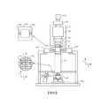
圖10為根據實施例的一微影投影裝置之示意圖。FIG. 10 is a schematic diagram of a lithography projection device according to an embodiment.
微影投影裝置可包括照明系統IL、第一物件台MT、第二物件台WT及投影系統PS。The lithography projection device may include an illumination system IL, a first object table MT, a second object table WT, and a projection system PS.
照明系統IL可調節輻射光束B。在此特定情況下,照明系統亦包含輻射源SO。The illumination system IL can adjust the radiation beam B. In this particular case, the lighting system also includes a radiation source SO.
第一物件台(例如,圖案化器件台)MT可具備用以固持圖案化器件MA(例如,倍縮光罩)之圖案化器件固持器,且連接至用以相對於項目PS來精準地定位圖案化器件之第一定位器。The first object stage (for example, the patterned device stage) MT may be provided with a patterned device holder for holding the patterned device MA (for example, a reduction mask), and is connected to be used for precise positioning relative to the item PS The first positioner for patterned devices.
第二物件台(基板台)WT可具備用以固持基板W(例如,抗蝕劑塗佈矽晶圓)之基板固持器,且連接至用以相對於項目PS來精準地定位該基板的第二定位器。The second object table (substrate table) WT may be provided with a substrate holder for holding the substrate W (for example, a resist-coated silicon wafer), and is connected to a second object table for accurately positioning the substrate with respect to the item PS Two locator.
投影系統(「透鏡」)PS(例如折射、反射或反射折射光學系統)可將圖案化器件MA之經照射部分成像至基板W之目標部分C(例如包含一或多個晶粒)上。The projection system ("lens") PS (such as a refractive, reflective, or catadioptric optical system) can image the illuminated portion of the patterned device MA onto the target portion C (such as containing one or more dies) of the substrate W.
如本文中所描繪,裝置可屬於透射類型(亦即,具有透射圖案化器件)。然而,一般而言,其亦可屬於反射類型,例如(具有反射圖案化器件)。裝置可使用與經典光罩不同種類之圖案化器件;實例包括可程式化鏡面陣列或LCD矩陣。As depicted herein, the device may be of the transmissive type (ie, have a transmissive patterned device). However, generally speaking, it can also belong to the reflective type, for example (with reflective patterned devices). The device can use different types of patterned devices from classic masks; examples include programmable mirror arrays or LCD matrixes.
源SO(例如,汞燈或準分子雷射、雷射產生電漿(LPP)EUV源)產生輻射光束。例如,此光束係直接地或在已橫穿諸如光束擴展器Ex之調節裝置之後饋入至照射系統(照射器)IL中。照射器IL可包含調整器件AD,以用於設定光束中之強度分佈之外部徑向範圍及/或內部徑向範圍(通常分別被稱作σ外部及σ內部)。另外,照明器IL通常將包含各種其他組件,諸如,積光器IN及聚光器CO。以此方式,照射於圖案化器件MA上之光束B在其橫截面中具有所要均一性及強度分佈。Source SO (for example, mercury lamp or excimer laser, laser generating plasma (LPP) EUV source) generates a radiation beam. For example, this light beam is fed into the illumination system (illuminator) IL directly or after having traversed an adjustment device such as a beam expander Ex. The illuminator IL may include an adjustment device AD for setting the outer radial range and/or the inner radial range (usually referred to as σ outer and σ inner, respectively) of the intensity distribution in the beam. In addition, the illuminator IL will generally include various other components, such as an accumulator IN and a condenser CO. In this way, the beam B irradiated on the patterned device MA has the desired uniformity and intensity distribution in its cross section.
在一些實施例中,源SO可在微影投影裝置之殼體內(如常常係當源SO為例如汞燈時的情況),但其亦可遠離微影投影裝置,源SO產生的輻射光束經引導至裝置中(例如藉助於合適之導向鏡);此後一情形可為當源SO為準分子雷射(例如基於KrF、ArF或F2雷射作用)時的情況。In some embodiments, the source SO may be in the housing of the lithography projection device (as is often the case when the source SO is, for example, a mercury lamp), but it can also be far away from the lithography projection device. The radiation beam generated by the source SO is passed through Guide into the device (for example by means of a suitable guide mirror); this latter case may be when the source SO is an excimer laser (for example based on KrF, ArF or F2 laser action).
光束PB可隨後截取被固持於圖案化器件台MT上之圖案化器件MA。在已橫穿圖案化器件MA的情況下,光束B傳遞通過透鏡PL,該透鏡PL將光束B聚焦至基板W之目標部分C上。藉助於第二定位裝置(及干涉式量測裝置IF),可精準地移動基板台WT,例如以便定位光束PB之路徑中的不同目標部分C。類似地,第一定位裝置可用以例如在自圖案化器件庫中機械擷取圖案化器件MA之後或在掃描期間相對於光束B之路徑精準地定位圖案化器件MA。一般而言,可藉助於長衝程模組(粗略定位)及短衝程模組(精細定位)來實現物件台MT、WT之移動。然而,在步進器(相對於步進掃描工具)之情況下,圖案化器件台MT可僅連接至短衝程致動器,或可固定。The light beam PB can then intercept the patterned device MA held on the patterned device table MT. Having traversed the patterned device MA, the light beam B passes through the lens PL, and the lens PL focuses the light beam B onto the target portion C of the substrate W. By means of the second positioning device (and the interferometric measuring device IF), the substrate table WT can be accurately moved, for example, in order to locate different target parts C in the path of the light beam PB. Similarly, the first positioning device can be used for example in self-patterningAfter mechanically picking up the patterned device MA in the device library or during scanning, the patterned device MA is accurately positioned relative to the path of the beam B. Generally speaking, a long-stroke module (coarse positioning) and a short-stroke module (fine positioning) can be used to realize the movement of the object table MT and WT. However, in the case of a stepper (as opposed to a step-and-scan tool), the patterned device table MT may be connected to only a short-stroke actuator, or may be fixed.
可在兩種不同模式(步進模式及掃描模式)中使用所描繪工具。在步進模式中,使圖案化器件台MT保持基本上靜止,且將整個圖案化器件影像一次性(亦即,單次「閃光」)投影至目標部分C上。接著可使基板台WT在x及/或y方向上移位,使得不同目標部分C可由光束PB照射。The drawn tool can be used in two different modes (step mode and scan mode). In the stepping mode, the patterned device stage MT is kept substantially still, and the entire patterned device image is projected onto the target portion C at one time (that is, a single "flash"). Then the substrate table WT can be shifted in the x and/or y direction, so that different target portions C can be irradiated by the light beam PB.
在掃描模式中,基本上相同的情形適用,惟不在單次「閃光」中曝光給定目標部分C除外。實際上,圖案化器件台MT可在給定方向(所謂「掃描方向」,例如,y方向)上以速度v移動,使得引起投影光束B在圖案化器件影像上進行掃描;同時發生地,基板台WT以速度V=Mv在相同或相對方向上同時地移動,其中M為透鏡PL之放大率(通常,M=1/4或=1/5)。以此方式,可在不必損害解析度的情況下曝光相對大目標部分C。In scanning mode, basically the same situation applies, except that the given target part C is not exposed in a single "flash". In fact, the patterned device stage MT can move at a speed v in a given direction (the so-called "scanning direction", for example, the y direction), causing the projection beam B to scan on the patterned device image; at the same time, the substrate The stage WT moves simultaneously in the same or opposite direction at a speed of V=Mv, where M is the magnification of the lens PL (usually, M=1/4 or =1/5). In this way, a relatively large target portion C can be exposed without compromising the resolution.
圖11為根據一實施例之另一微影投影裝置(LPA)的示意圖。FIG. 11 is a schematic diagram of another lithographic projection apparatus (LPA) according to an embodiment.
LPA可包括源收集器模組SO、經組態以調節輻射光束B(例如EUV輻射)的照明系統(照明器)IL、支撐結構MT、基板台WT及投影系統PS。The LPA may include a source collector module SO, an illumination system (illuminator) IL configured to adjust the radiation beam B (for example, EUV radiation), a support structure MT, a substrate table WT, and a projection system PS.
支撐結構(例如,圖案化器件台)MT可經建構以支撐圖案化器件(例如,光罩或倍縮光罩)MA且連接至經組態以精準地定位圖案化器件之第一定位器PM;基板台(例如,晶圓台)WT可經建構以固持基板(例如,抗蝕劑塗佈晶圓)W,且連接至經組態以精準地定位該基板之第二定位器PM。The support structure (e.g., patterned device stage) MT can be constructed to support the patterned device (e.g., mask or reduction mask) MA and connected to the configured to accurately position the patternedThe first positioner PM of the device; the substrate table (eg, wafer table) WT can be constructed to hold the substrate (eg, resist coated wafer) W, and is connected to a substrate configured to accurately position the substrate The second positioner PM.
投影系統(例如,反射性投影系統)PS可經組態以將藉由圖案化器件MA賦予給輻射光束B之圖案投影於基板W的目標部分C(例如,包含一或多個晶粒)上。The projection system (for example, a reflective projection system) PS can be configured to project the pattern imparted to the radiation beam B by the patterning device MA on the target portion C (for example, including one or more dies) of the substrate W .
如此處所描繪,LPA可屬於反射類型(例如,採用反射圖案化器件)。應注意,因為大多數材料在EUV波長範圍內具吸收性,所以圖案化器件可具有包含(例如)鉬與矽之多堆疊的多層反射器。在一個實例中,多堆疊反射器具有鉬與矽之40個層對,其中每一層之厚度為四分之一波長。可運用X射線微影來產生更小波長。由於大多數材料在EUV及x射線波長下具吸收性,因此圖案化器件構形上的圖案化吸收材料之薄件(例如,在多層反射器的頂部上之TaN吸收體)界定特徵將印刷(正型抗蝕劑)或不印刷(負性抗蝕劑)在何處。As depicted here, LPA can be of the reflective type (for example, using reflective patterned devices). It should be noted that because most materials are absorptive in the EUV wavelength range, the patterned device may have a multilayer reflector containing, for example, many stacks of molybdenum and silicon. In one example, the multi-stack reflector has 40 layer pairs of molybdenum and silicon, where the thickness of each layer is a quarter wavelength. X-ray lithography can be used to produce smaller wavelengths. Since most materials are absorptive at EUV and X-ray wavelengths, a thin piece of patterned absorbing material (for example, a TaN absorber on top of a multilayer reflector) defining features on the patterned device configuration will be printed ( Where is the positive resist) or no printing (negative resist).
照明器IL可自源收集器模組SO接收極紫外線輻射光束。用以產生EUV輻射之方法包括但不一定限於藉由EUV範圍中之一或多個發射譜線將材料轉換成具有至少一個元素之電漿狀態,元素例如氙、鋰或錫。在一種此類方法(常常被稱為雷射產生電漿(「LPP」))中,可藉由運用雷射光束來照射燃料(諸如,具有譜線發射元素之材料小滴、串流或叢集)而產生電漿。源收集器模組SO可為包括雷射之EUV輻射系統之部分,該雷射用於提供激發燃料之雷射光束。所得電漿發射輸出輻射,例如EUV輻射,該輻射係使用安置於源收集器模組中之輻射收集器予以收集。舉例而言,當使用CO2雷射以提供用於燃料激發之雷射光束時,雷射及源收集器模組可為分離實體。The illuminator IL can receive the extreme ultraviolet radiation beam from the source collector module SO. Methods for generating EUV radiation include, but are not necessarily limited to, converting the material into a plasma state with at least one element, such as xenon, lithium, or tin, by one or more emission lines in the EUV range. In one such method (often referred to as laser-generated plasma ("LPP")), a laser beam can be used to irradiate fuel (such as droplets, streams, or clusters of materials with line-emitting elements). ) To produce plasma. The source collector module SO may be part of an EUV radiation system including a laser used to provide a laser beam for exciting fuel. The resulting plasma emits output radiation, such as EUV radiation, which is collected using a radiation collector placed in the source collector module. For exampleIn other words, when a CO2 laser is used to provide a laser beam for fuel excitation, the laser and the source collector module can be separate entities.
在此類情況下,不認為雷射形成微影裝置之部件,且輻射光束可藉助於包含例如合適導向鏡及/或光束擴展器之光束遞送系統而自雷射傳遞至源收集器模組。在其他情況下,舉例而言,當源為放電產生電漿EUV產生器(常常被稱為DPP源)時,源可為源收集器模組之整體部件。In such cases, the laser is not considered to form a part of the lithography device, and the radiation beam can be transmitted from the laser to the source collector module by means of a beam delivery system including, for example, a suitable guide mirror and/or beam expander. In other cases, for example, when the source is a discharge generating plasma EUV generator (often referred to as a DPP source), the source can be an integral part of the source collector module.
照明器IL可包含用於調整輻射光束之角強度分佈的調整器。一般而言,可調整照明器之光瞳平面中之強度分佈的至少外部徑向範圍及/或內部徑向範圍(通常分別稱作σ外部及σ內部)。另外,照明器IL可包含各種其他組件,諸如琢面化場鏡面器件及琢面化光瞳鏡面器件。照明器可用以調節輻射光束,以在其橫截面中具有所要均一性及強度分佈。The illuminator IL may include an adjuster for adjusting the angular intensity distribution of the radiation beam. Generally speaking, at least the outer radial range and/or the inner radial range (usually referred to as σ outer and σ inner, respectively) of the intensity distribution in the pupil plane of the illuminator can be adjusted. In addition, the illuminator IL may include various other components, such as a faceted field mirror device and a faceted pupil mirror device. The illuminator can be used to adjust the radiation beam to have the desired uniformity and intensity distribution in its cross section.
輻射光束B入射於被固持於支撐結構(例如,圖案化器件台)MT上之圖案化器件(例如,光罩)MA上,且係由該圖案化器件而圖案化。在自圖案化器件(例如,光罩)MA反射之後,輻射光束B傳遞通過投影系統PS,投影系統PS將該光束聚焦至基板W之目標部分C上。藉助於第二定位器PW及位置感測器PS2(例如,干涉量測器件、線性編碼器或電容式感測器),可精準地移動基板台WT,(例如)以便使不同目標部分C定位於輻射光束B之路徑中。類似地,第一定位器PM及另一位置感測器PS1可用以相對於輻射光束B之路徑來精準地定位圖案化器件(例如,光罩)MA。可使用圖案化器件對準標記M1、M2及基板對準標記P1、P2來對準圖案化器件(例如,光罩)MA及基板W。The radiation beam B is incident on the patterned device (eg, photomask) MA held on the support structure (eg, patterned device table) MT, and is patterned by the patterned device. After being reflected from the patterned device (eg, mask) MA, the radiation beam B passes through the projection system PS, and the projection system PS focuses the beam onto the target portion C of the substrate W. With the aid of the second positioner PW and the position sensor PS2 (for example, an interferometric measuring device, a linear encoder or a capacitive sensor), the substrate table WT can be accurately moved, for example, to position different target parts C In the path of the radiation beam B. Similarly, the first positioner PM and the other position sensor PS1 can be used to accurately position the patterned device (for example, a mask) MA relative to the path of the radiation beam B. The patterned device alignment marks M1, M2 and the substrate alignment marks P1, P2 may be used to align the patterned device (for example, a photomask) MA and the substrate W.
所描繪裝置LPA可用於以下模式中之至少一者:步進模式、掃描模式及靜止模式。The depicted device LPA can be used in at least one of the following modes: step mode, scan mode, and static mode.
在步進模式中,在將被賦予至輻射光束之整個圖案一次性投影至目標部分C上時,使支撐結構(例如,圖案化器件台)MT及基板台WT保持基本上靜止(亦即,單次靜態曝光)。接著,使基板台WT在X及/或Y方向上移位,使得可曝光不同目標部分C。In the stepping mode, when the entire pattern imparted to the radiation beam is projected onto the target portion C at one time, the support structure (for example, the patterned device table) MT and the substrate table WT are kept substantially stationary (ie, Single static exposure). Then, the substrate table WT is shifted in the X and/or Y direction, so that different target portions C can be exposed.
在掃描模式中,在將被賦予至輻射光束之圖案投影至目標部分C上時,同步地掃描支撐結構(例如,圖案化器件台)MT及基板台WT(亦即,單次動態曝光)。可藉由投影系統PS之放大率(縮小率)及影像反轉特性來判定基板台WT相對於支撐結構(例如,圖案化器件台)MT之速度及方向。In the scanning mode, when the pattern imparted to the radiation beam is projected onto the target portion C, the support structure (for example, the patterned device stage) MT and the substrate stage WT are simultaneously scanned (ie, a single dynamic exposure). The speed and direction of the substrate table WT relative to the support structure (for example, the patterned device table) MT can be determined by the magnification (reduction ratio) and image reversal characteristics of the projection system PS.
在靜止模式中,在將被賦予至輻射光束之圖案投影至目標部分C上時,使支撐結構(例如,圖案化器件台)MT保持基本上靜止,從而固持可程式化圖案化器件,且移動或掃描基板台WT。在此模式中,通常採用脈衝式輻射源,且在基板台WT之每一移動之後或在掃描期間之逐次輻射脈衝之間視需要而更新可程式化圖案化器件。此操作模式可易於應用於利用可程式化圖案化器件(諸如,可程式化鏡面陣列)之無光罩微影。In the stationary mode, when the pattern imparted to the radiation beam is projected onto the target portion C, the support structure (for example, the patterned device table) MT is kept substantially stationary, thereby holding the programmable patterned device and moving Or scan the substrate table WT. In this mode, a pulsed radiation source is usually used, and the programmable patterned device is updated as needed after each movement of the substrate table WT or between successive radiation pulses during scanning. This mode of operation can be easily applied to maskless lithography using programmable patterned devices (such as programmable mirror arrays).
圖12為根據一實施例之微影投影裝置的詳細視圖。FIG. 12 is a detailed view of a lithography projection apparatus according to an embodiment.
如所示,LPA可包括源收集器模組SO、照明系統IL及投影系統PS。源收集器模組SO經建構及配置成使得可將真空環境維持於源收集器模組SO之圍封結構ES中。可藉由放電產生電漿源而形成EUV輻射發射熱電漿HP。可藉由氣體或蒸汽(例如,Xe氣體、Li蒸汽或Sn蒸汽)而產生EUV輻射,其中產生熱電漿HP以發射在電磁波譜之EUV範圍內之輻射。舉例而言,藉由引起至少部分離子化電漿之放電來產生熱電漿HP。為了輻射之有效率產生,可需要為(例如)10帕斯卡(Pa)之分壓之Xe、Li、Sn蒸汽或任何其他合適氣體或蒸汽。在一實施例中,提供經激發錫(Sn)電漿以產生EUV輻射。As shown, the LPA may include a source collector module SO, an illumination system IL, and a projection system PS. The source collector module SO is constructed and configured such that a vacuum environment can be maintained in the enclosure structure ES of the source collector module SO. The EUV radiation emitting thermoplasma HP can be formed by generating a plasma source by discharge. EUV radiation can be generated by gas or steam (for example, Xe gas, Li steam or Sn steam), wherein thermoplasma HP is generated to emit radiation in the EUV range of the electromagnetic spectrum. For example, the thermoplasma HP is generated by causing at least part of the discharge of ionized plasma. In order to generate radiation efficiently, it may need to be (for example) Xe, a partial pressure of 10 Pascals (Pa),Li, Sn steam or any other suitable gas or steam. In one embodiment, an excited tin (Sn) plasma is provided to generate EUV radiation.
由熱電漿HP發射之輻射係經由定位於源腔室SC中之開口中或後方的視情況選用之氣體障壁或污染物截留器CT(在一些情況下,其亦被稱作污染物障壁或箔片截留器)而自源腔室SC傳遞至收集器腔室CC中。污染物截留器CT可包括溝道結構。污染物截留器CT亦可包括氣體障壁,或氣體障壁與溝道結構之組合。如在此項技術中為吾人所知,本文中進一步所指示之污染物截留器或污染物障壁CT至少包括溝道結構。The radiation emitted by the thermoplasma HP passes through an optional gas barrier or pollutant trap CT located in or behind the opening in the source chamber SC (in some cases, it is also called a pollutant barrier or foil The slice trap is transferred from the source chamber SC to the collector chamber CC. The pollutant trap CT may include a channel structure. The pollutant trap CT may also include a gas barrier or a combination of a gas barrier and a channel structure. As known in the art, the pollutant trap or pollutant barrier CT further indicated herein includes at least a channel structure.
收集器腔室CC可包括可為所謂的掠入射收集器之輻射收集器CO。輻射收集器CO具有上游輻射收集器側US及下游輻射收集器側DS。橫穿輻射收集器CO之輻射可自光柵光譜濾光器SF反射以沿著由點虛線「O」指示之光軸聚焦於虛擬源點IF中。虛擬源點IF可被稱作中間焦點,且源收集器模組可經配置使得中間焦點IF位於圍封結構ES中之開口OP處或附近。虛擬源點IF為輻射發射電漿HP之影像。The collector chamber CC may include a radiation collector CO, which may be a so-called grazing incidence collector. The radiation collector CO has an upstream radiation collector side US and a downstream radiation collector side DS. The radiation traversing the radiation collector CO can be reflected from the grating spectral filter SF to focus in the virtual source point IF along the optical axis indicated by the dotted dotted line "O". The virtual source point IF may be referred to as an intermediate focus, and the source collector module may be configured such that the intermediate focus IF is located at or near the opening OP in the enclosure structure ES. The virtual source point IF is the image of the radiation emission plasma HP.
隨後,輻射橫穿照明系統IL,照明系統IL可包括琢面化場鏡面器件FM及琢面化光瞳鏡面器件pm,琢面化場鏡面器件FM及琢面化光瞳鏡面器件pm經配置以提供在圖案化器件MA處輻射光束B之所要角度分佈,以及在圖案化器件MA處之輻射振幅之所要均一性。在由支撐結構MT固持之圖案化器件MA處的輻射光束B之反射後,形成經圖案化光束PB,且藉由投影系統PS經由反射元件RE將經圖案化光束PB成像至由基板台WT固持之基板W上。Subsequently, the radiation traverses the illumination system IL. The illumination system IL may include a faceted field mirror device FM and a faceted pupil mirror device pm. The faceted field mirror device FM and a faceted pupil mirror device pm are configured to Provide the desired angular distribution of the radiation beam B at the patterned device MA and the desired uniformity of the radiation amplitude at the patterned device MA. After the reflection of the radiation beam B at the patterned device MA held by the support structure MT, a patterned beam PB is formed, and the patterned beam PB is imaged by the projection system PS through the reflective element RE to be held by the substrate table WT On the substrate W.
照明光學件單元IL及投影系統PS中通常可存在比所示更多的元件。取決於微影裝置之類型,光柵光譜濾光器SF可視情況存在。此外,可存在比諸圖中所展示之鏡面更多的鏡面,例如,在投影系統PS中可存在1至6個額外反射元件。There may usually be more elements than shown in the illumination optics unit IL and the projection system PS. Depending on the type of lithography device, the grating spectral filter SF may be present. thisIn addition, there may be more mirrors than those shown in the figures, for example, there may be 1 to 6 additional reflective elements in the projection system PS.
收集器光學件CO可為具有掠入射反射器GR之巢套式收集器,僅作為收集器(或收集器鏡面)之實例。掠入射反射器GR經安置為圍繞光軸O軸向對稱,且此類型之收集器光學件CO可與常常被稱為DPP源之放電產生電漿源組合使用。The collector optics CO can be a nested collector with a grazing incidence reflector GR, which is only an example of a collector (or collector mirror). The grazing incidence reflector GR is arranged to be axially symmetrical around the optical axis O, and this type of collector optics CO can be used in combination with a discharge-generating plasma source often referred to as a DPP source.
圖13為根據一實施例的微影投影裝置LPA之源收集器模組SO的詳細視圖。FIG. 13 is a detailed view of the source collector module SO of the lithographic projection apparatus LPA according to an embodiment.
源收集器模組SO可為LPA輻射系統之部分。雷射LA可經配置以將雷射能量沈積至諸如氙(Xe)、錫(Sn)或鋰(Li)之燃料中,從而產生具有數十電子伏特(eV)的電子溫度之高度離子化電漿HP。在此等離子之去激發及再結合期間產生之高能輻射係自電漿發射、由近正入射收集器光學件CO收集,且聚焦至圍封結構ES中之開口OP上。The source collector module SO can be part of the LPA radiation system. Laser LA can be configured to deposit laser energy into fuels such as xenon (Xe), tin (Sn), or lithium (Li), thereby generating highly ionized electricity with an electron temperature of tens of electron volts (eV) Pulp HP. The high-energy radiation generated during the de-excitation and recombination of the plasma is emitted from the plasma, collected by the near-normal incidence collector optics CO, and focused on the opening OP in the enclosure structure ES.
可以使用以下條項進一步描述實施例:The following items can be used to further describe the embodiments:
1.一種用於藉由量測部分地基於一目標設計建構之一經印刷設計上之一特徵而改善一製程模型之方法,該方法包含:獲得a)來自一影像捕捉器件的該經印刷設計之一影像及b)基於該影像中之形狀的輪廓;藉由一圖案識別程式鑑別該目標設計上之包括該特徵的圖案;判定該等輪廓上之對應於該特徵的座標;及藉由至少a)基於該等座標來提供該特徵之一量測及b)基於該量測與該目標設計中之一對應特徵的一比較來校準該製程模型而改善該製程模型。1. A method for improving a process model by measuring a feature of a printed design based in part on a target design, the method comprising: obtaining a) the printed design from an image capture device An image and b) a contour based on the shape in the image; identifying the pattern including the feature on the target design by a pattern recognition program; determining the coordinates on the contour corresponding to the feature; and by at least a ) Provide a measurement of the feature based on the coordinates and b) calibrate the process model based on a comparison of the measurement with a corresponding feature in the target design to improve the process model.
2.如條項1之方法,其中該特徵為一邊緣置放量規或一臨界尺寸中之至少一者。2. The method of
3.如條項1之方法,其中該等座標為邊緣置放量規或臨界尺寸之座標。3. As in the method of
4.如條項1之方法,其中該量測係藉由對該等座標進行平均來產生。4. The method of
5.如條項1之方法,其中該特徵包含該經印刷設計上之一曲率、一深度、一角度、一帶寬及一斜率中之至少一者。5. The method of
6.如條項1之方法,其中該特徵包含該影像之一對比度及一強度中之至少一者。6. The method of
7.如條項1之方法,其進一步包含自該影像產生該等輪廓。7. The method of
8.如條項7之方法,其進一步包含至少基於該目標設計與該等輪廓之間的一比較來對準該影像與該目標設計。8. The method of clause 7, further comprising aligning the image with the target design based at least on a comparison between the target design and the contours.
9.如條項7之方法,其進一步包含橫越該目標設計中之一或多個平行線產生水平或豎直切線。9. The method of clause 7, further comprising generating horizontal or vertical tangents across one or more parallel lines in the target design.
10.如條項9之方法,其進一步包含至少基於該水平或豎直切線與該等輪廓之一相交而判定一臨界尺寸。10. The method of clause 9, further comprising determining a critical dimension based at least on the intersection of the horizontal or vertical tangent with one of the contours.
11.如條項7之方法,其進一步包含產生自該目標設計中之一點延伸的一傾斜切線。11. The method of clause 7, further comprising generating an oblique tangent line extending from a point in the target design.
12.如條項11之方法,其進一步包含至少基於該傾斜切線與該等輪廓之一相交而產生一EP量規。12. The method of
13.如條項1之方法,其進一步包含接收指定沿著該等圖案之一部分的切線之一密度的使用者輸入,該密度對應於沿著該部分的每單位長度之切線的一數目。13. The method of
14.如條項1之方法,其進一步包含:自該目標設計定位與該圖案相同之其他圖案;及自該等其他圖案判定該等座標。14. The method of
15.如條項14之方法,其中該定位係進一步基於來自該目標設計之多邊形的座標之一比較。15. The method of clause 14, wherein the positioning is further based on a comparison of one of the coordinates of the polygon from the target design.
16.如條項1之方法,其進一步包含:在該圖案識別程式處接收一第一圖案及一第二圖案;基於該第一圖案及該第二圖案中之複數個座標判定該第一圖案及該第二圖案是否相同;及至少基於該第一圖案及該第二圖案判定該量測。16. The method of
17.如條項16之方法,其進一步包含當判定該第一圖案及該第二圖案是否相同時考慮該第一圖案相對於該第二圖案的一平移或一旋轉中之一或多者。17. The method of clause 16, further comprising considering one or more of a translation or a rotation of the first pattern relative to the second pattern when determining whether the first pattern and the second pattern are the same.
18.如條項1之方法,其中該圖案識別程式基於具有零變化之一精確匹配鑑別其他圖案。18. The method of
19.如條項1之方法,其中該圖案識別程式基於一模糊匹配鑑別其他圖案。19. The method of
20.如條項19之方法,其中該模糊匹配允許其他圖案中之該等座標之間的高達2nm變化。20. The method of clause 19, wherein the fuzzy matching allows up to 2nm variation between the coordinates in other patterns.
21.一種用於藉由量測部分地基於一目標設計建構之一經印刷設計上之一特徵校準一光學近接校正模型之方法,該方法包含:獲得a)來自一掃描電子顯微鏡之該經印刷設計的一影像及b)基於該影像中之形狀的輪廓;藉由一圖案識別程式鑑別該目標設計上之包括該特徵的圖案;判定該等輪廓上之對應於該特徵的座標;及藉由至少a)基於該等座標來提供該特徵之一量測及b)基於該量測與該目標設計中之一對應特徵的一比較來校準該製程模型而改善該光學近接校正模型。21. A method for calibrating an optical proximity correction model based on a feature of a printed design constructed partly based on a target design by measurement, the method comprising: obtaining a) the printed design from a scanning electron microscope An image of and b) an outline based on the shape in the image;Identify the pattern that includes the feature on the target design by a pattern recognition program; determine the coordinates on the outlines corresponding to the feature; and by at least a) providing a measurement of the feature based on the coordinates and b) Calibrating the process model based on a comparison between the measurement and a corresponding feature in the target design to improve the optical proximity correction model.
22.一種電腦程式產品,其包含經記錄有指令之一非暫時性電腦可讀媒體,該等指令在由一電腦執行時實施以上條項中任一項之方法。22. A computer program product comprising a non-transitory computer-readable medium with recorded instructions that, when executed by a computer, implement the method of any one of the above items.
本文中所揭示之概念可模擬或數學上模型化用於使子波長特徵成像之任何通用成像系統,且可尤其供能夠產生愈來愈短波長之新興成像技術使用。已經在使用中之新興技術包括能夠藉由使用ArF雷射來產生193nm波長且甚至能夠藉由使用氟雷射來產生157nm波長之極紫外線(EUV)、DUV微影。此外,EUV微影能夠藉由使用同步加速器或藉由運用高能電子來撞擊材料(固體或電漿)而產生在20nm至50nm之範圍內之波長,以便產生在此範圍內之光子。The concepts disclosed herein can simulate or mathematically model any general imaging system for imaging sub-wavelength features, and can be used especially for emerging imaging technologies capable of generating shorter and shorter wavelengths. Emerging technologies that are already in use include the ability to generate 193nm wavelength by using ArF laser and even extreme ultraviolet (EUV) and DUV lithography with 157nm wavelength by using fluorine laser. In addition, EUV lithography can generate wavelengths in the range of 20nm to 50nm by using a synchrotron or by using high-energy electrons to strike a material (solid or plasma) to generate photons in this range.
雖然本文中所揭示之概念可用於在諸如矽晶圓之基板上的成像,但應理解,所揭示之概念可與任何類型之微影成像系統一起使用,例如,用於在不同於矽晶圓的基板上之成像的微影成像系統。Although the concepts disclosed in this article can be used for imaging on substrates such as silicon wafers, it should be understood that the concepts disclosed can be used with any type of lithography imaging system, for example, for imaging applications other than silicon wafers. The photolithography imaging system for imaging on the substrate.
以上描述意欲為說明性,而非限制性的。因此,對於熟習此項技術者將顯而易見,可在不脫離下文所闡明之申請專利範圍之範疇的情況下如所描述進行修改。The above description is intended to be illustrative, not restrictive. Therefore, it will be obvious to those who are familiar with the technology that they can be modified as described without departing from the scope of the patent application explained below.
510:目標設計510: target design
520:例示性圖案520: Illustrative pattern
530:第一圖案530: first pattern
540:切線540: Tangent
Claims (15)
Translated fromChineseApplications Claiming Priority (2)
| Application Number | Priority Date | Filing Date | Title |
|---|---|---|---|
| US201862697169P | 2018-07-12 | 2018-07-12 | |
| US62/697,169 | 2018-07-12 |
Publications (2)
| Publication Number | Publication Date |
|---|---|
| TW202006317A TW202006317A (en) | 2020-02-01 |
| TWI714165Btrue TWI714165B (en) | 2020-12-21 |
Family
ID=67137913
Family Applications (1)
| Application Number | Title | Priority Date | Filing Date |
|---|---|---|---|
| TW108124603ATWI714165B (en) | 2018-07-12 | 2019-07-12 | Method for improving a process model |
Country Status (5)
| Country | Link |
|---|---|
| US (1) | US11422473B2 (en) |
| KR (1) | KR102609413B1 (en) |
| CN (1) | CN112424694B (en) |
| TW (1) | TWI714165B (en) |
| WO (1) | WO2020011513A1 (en) |
Cited By (1)
| Publication number | Priority date | Publication date | Assignee | Title |
|---|---|---|---|---|
| TWI870671B (en)* | 2021-06-23 | 2025-01-21 | 荷蘭商Asml荷蘭公司 | Method and system for determining an etch effect for a substrate pattern and releated non-transitory computer readable medium |
Families Citing this family (3)
| Publication number | Priority date | Publication date | Assignee | Title |
|---|---|---|---|---|
| CN113454533B (en)* | 2019-02-25 | 2025-04-01 | Asml荷兰有限公司 | Method for determining random variations in printed patterns |
| KR20250051134A (en) | 2019-05-21 | 2025-04-16 | 에이에스엠엘 네델란즈 비.브이. | Method for determining stochastic variation associated with desired pattern |
| US12062885B2 (en)* | 2019-07-25 | 2024-08-13 | Trinamix Gmbh | Light module and a method for its operation |
Citations (4)
| Publication number | Priority date | Publication date | Assignee | Title |
|---|---|---|---|---|
| US20120110522A1 (en)* | 2010-10-28 | 2012-05-03 | International Business Machines Corporation | Pattern Recognition with Edge Correction for Design Based Metrology |
| US20170082927A1 (en)* | 2014-03-18 | 2017-03-23 | Asml Netherlands B.V. | Pattern placement error aware optimization |
| WO2017060192A1 (en)* | 2015-10-08 | 2017-04-13 | Asml Netherlands B.V. | Method and apparatus for pattern correction and verification |
| TW201800871A (en)* | 2016-03-24 | 2018-01-01 | Asml荷蘭公司 | Optimization of a lithographic projection apparatus accounting for an interlayer characteristic |
Family Cites Families (16)
| Publication number | Priority date | Publication date | Assignee | Title |
|---|---|---|---|---|
| US5229872A (en) | 1992-01-21 | 1993-07-20 | Hughes Aircraft Company | Exposure device including an electrically aligned electronic mask for micropatterning |
| WO1997033205A1 (en) | 1996-03-06 | 1997-09-12 | Philips Electronics N.V. | Differential interferometer system and lithographic step-and-scan apparatus provided with such a system |
| US7747978B2 (en) | 2005-08-08 | 2010-06-29 | Asml Netherlands B.V. | System and method for creating a focus-exposure model of a lithography process |
| US7695876B2 (en) | 2005-08-31 | 2010-04-13 | Brion Technologies, Inc. | Method for identifying and using process window signature patterns for lithography process control |
| WO2007030704A2 (en) | 2005-09-09 | 2007-03-15 | Brion Technologies, Inc. | System and method for mask verification using an individual mask error model |
| US7694267B1 (en) | 2006-02-03 | 2010-04-06 | Brion Technologies, Inc. | Method for process window optimized optical proximity correction |
| US7882480B2 (en) | 2007-06-04 | 2011-02-01 | Asml Netherlands B.V. | System and method for model-based sub-resolution assist feature generation |
| US7707538B2 (en) | 2007-06-15 | 2010-04-27 | Brion Technologies, Inc. | Multivariable solver for optical proximity correction |
| US20090157630A1 (en) | 2007-10-26 | 2009-06-18 | Max Yuan | Method of extracting data and recommending and generating visual displays |
| KR100914297B1 (en)* | 2007-12-28 | 2009-08-27 | 주식회사 하이닉스반도체 | Optical Proximity Effect Correction Method Using Wafer Pattern Measurement Data |
| KR20090071737A (en)* | 2007-12-28 | 2009-07-02 | 주식회사 하이닉스반도체 | Pattern Layout Correction Method Using Wafer Pattern Measurement Data |
| NL2003699A (en) | 2008-12-18 | 2010-06-21 | Brion Tech Inc | Method and system for lithography process-window-maximixing optical proximity correction. |
| KR20100135093A (en)* | 2009-06-16 | 2010-12-24 | 주식회사 하이닉스반도체 | Pattern error detection method of semiconductor device |
| US8607168B2 (en)* | 2010-02-16 | 2013-12-10 | Mentor Graphics Corporation | Contour alignment for model calibration |
| US9646220B2 (en)* | 2013-11-25 | 2017-05-09 | GlobalFoundries, Inc. | Methods and media for averaging contours of wafer feature edges |
| US8938695B1 (en)* | 2014-01-09 | 2015-01-20 | Dmo Systems Limited | Signature analytics for improving lithographic process of manufacturing semiconductor devices |
- 2019
- 2019-06-21CNCN201980046453.9Apatent/CN112424694B/enactiveActive
- 2019-06-21WOPCT/EP2019/066520patent/WO2020011513A1/ennot_activeCeased
- 2019-06-21KRKR1020217000779Apatent/KR102609413B1/enactiveActive
- 2019-06-21USUS17/256,332patent/US11422473B2/enactiveActive
- 2019-07-12TWTW108124603Apatent/TWI714165B/enactive
Patent Citations (5)
| Publication number | Priority date | Publication date | Assignee | Title |
|---|---|---|---|---|
| US20120110522A1 (en)* | 2010-10-28 | 2012-05-03 | International Business Machines Corporation | Pattern Recognition with Edge Correction for Design Based Metrology |
| US20170082927A1 (en)* | 2014-03-18 | 2017-03-23 | Asml Netherlands B.V. | Pattern placement error aware optimization |
| WO2017060192A1 (en)* | 2015-10-08 | 2017-04-13 | Asml Netherlands B.V. | Method and apparatus for pattern correction and verification |
| TW201721280A (en)* | 2015-10-08 | 2017-06-16 | Asml荷蘭公司 | Method and apparatus for pattern correction and verification |
| TW201800871A (en)* | 2016-03-24 | 2018-01-01 | Asml荷蘭公司 | Optimization of a lithographic projection apparatus accounting for an interlayer characteristic |
Cited By (1)
| Publication number | Priority date | Publication date | Assignee | Title |
|---|---|---|---|---|
| TWI870671B (en)* | 2021-06-23 | 2025-01-21 | 荷蘭商Asml荷蘭公司 | Method and system for determining an etch effect for a substrate pattern and releated non-transitory computer readable medium |
Also Published As
| Publication number | Publication date |
|---|---|
| KR20210020086A (en) | 2021-02-23 |
| KR102609413B1 (en) | 2023-12-04 |
| US20210263426A1 (en) | 2021-08-26 |
| CN112424694A (en) | 2021-02-26 |
| TW202006317A (en) | 2020-02-01 |
| US11422473B2 (en) | 2022-08-23 |
| WO2020011513A1 (en) | 2020-01-16 |
| CN112424694B (en) | 2023-10-20 |
Similar Documents
| Publication | Publication Date | Title |
|---|---|---|
| TWI711900B (en) | Method for improving a process model for a patterning process and related computer program product | |
| CN112602020B (en) | Automatic selection of high-quality average SEM images from raw images using machine learning | |
| CN114096917B (en) | Prediction data selection for model calibration to reduce uncertainty in model predictions | |
| TWI718771B (en) | Methods, computer program product, and systems for reducing variability of an error associated with a structure on a wafer | |
| TW202006346A (en) | Hidden defect detection and EPE estimation based on the extracted 3D information from e-beam images | |
| TWI714165B (en) | Method for improving a process model | |
| TWI702467B (en) | Systems, methods and computer program products for improving resist model predictions | |
| CN116057466A (en) | Apparatus and method for selecting information patterns to train a machine learning model | |
| TW201837613A (en) | Methods of guiding process models and inspection in a manufacturing process | |
| TWI661264B (en) | Methods of tuning process models | |
| TW202101126A (en) | Improve gauge selection for model calibration | |
| TWI667553B (en) | Methods of determining characteristics of a pattern | |
| TWI839015B (en) | Methods, software, and systems for determination of constant-width sub-resolution assist features | |
| US20250264808A1 (en) | Diffraction-based pupil determination for optimization of lithographic processes | |
| CN120051731A (en) | Source optimization for mitigating mask error effects | |
| CN118525250A (en) | Software, method and system for determining local focus | |
| TW202127147A (en) | Method and system for enhancing target features of a pattern imaged onto a substrate |