TWI713221B - High electron mobility transistor and methods for forming the same - Google Patents
High electron mobility transistor and methods for forming the sameDownload PDFInfo
- Publication number
- TWI713221B TWI713221BTW107137949ATW107137949ATWI713221BTW I713221 BTWI713221 BTW I713221BTW 107137949 ATW107137949 ATW 107137949ATW 107137949 ATW107137949 ATW 107137949ATW I713221 BTWI713221 BTW I713221B
- Authority
- TW
- Taiwan
- Prior art keywords
- layer
- gallium nitride
- mobility transistor
- electron mobility
- high electron
- Prior art date
Links
- 238000000034methodMethods0.000titleclaimsdescription13
- 229910002601GaNInorganic materials0.000claimsabstractdescription123
- JMASRVWKEDWRBT-UHFFFAOYSA-NGallium nitrideChemical compound[Ga]#NJMASRVWKEDWRBT-UHFFFAOYSA-N0.000claimsabstractdescription99
- 239000000758substrateSubstances0.000claimsabstractdescription28
- RNQKDQAVIXDKAG-UHFFFAOYSA-Naluminum galliumChemical compound[Al].[Ga]RNQKDQAVIXDKAG-UHFFFAOYSA-N0.000claimsdescription26
- 230000004888barrier functionEffects0.000claimsdescription18
- 230000006911nucleationEffects0.000claimsdescription17
- 238000010899nucleationMethods0.000claimsdescription17
- 238000004519manufacturing processMethods0.000claimsdescription16
- PMHQVHHXPFUNSP-UHFFFAOYSA-Mcopper(1+);methylsulfanylmethane;bromideChemical compoundBr[Cu].CSCPMHQVHHXPFUNSP-UHFFFAOYSA-M0.000claimsdescription15
- 229910052782aluminiumInorganic materials0.000claimsdescription9
- XAGFODPZIPBFFR-UHFFFAOYSA-NaluminiumChemical group[Al]XAGFODPZIPBFFR-UHFFFAOYSA-N0.000claimsdescription9
- PIGFYZPCRLYGLF-UHFFFAOYSA-NAluminum nitrideChemical compound[Al]#NPIGFYZPCRLYGLF-UHFFFAOYSA-N0.000claimsdescription7
- 150000004767nitridesChemical class0.000claimsdescription3
- IWBUYGUPYWKAMK-UHFFFAOYSA-N[AlH3].[N]Chemical compound[AlH3].[N]IWBUYGUPYWKAMK-UHFFFAOYSA-N0.000claims1
- 229910052733galliumInorganic materials0.000claims1
- OKTJSMMVPCPJKN-UHFFFAOYSA-NCarbonChemical compound[C]OKTJSMMVPCPJKN-UHFFFAOYSA-N0.000abstractdescription8
- 229910052799carbonInorganic materials0.000abstractdescription8
- 239000010410layerSubstances0.000description280
- 239000000463materialSubstances0.000description14
- 238000005229chemical vapour depositionMethods0.000description9
- 238000004943liquid phase epitaxyMethods0.000description9
- 230000015572biosynthetic processEffects0.000description8
- 238000000151depositionMethods0.000description8
- 238000005137deposition processMethods0.000description8
- 238000001451molecular beam epitaxyMethods0.000description8
- 239000013078crystalSubstances0.000description7
- 229910052751metalInorganic materials0.000description7
- 239000002184metalSubstances0.000description7
- 239000004065semiconductorSubstances0.000description6
- 230000005533two-dimensional electron gasEffects0.000description6
- 230000008569processEffects0.000description4
- 230000003746surface roughnessEffects0.000description3
- IJGRMHOSHXDMSA-UHFFFAOYSA-NAtomic nitrogenChemical compoundN#NIJGRMHOSHXDMSA-UHFFFAOYSA-N0.000description2
- 238000010586diagramMethods0.000description2
- 125000002524organometallic groupChemical group0.000description2
- 238000006467substitution reactionMethods0.000description2
- XUIMIQQOPSSXEZ-UHFFFAOYSA-NSiliconChemical compound[Si]XUIMIQQOPSSXEZ-UHFFFAOYSA-N0.000description1
- 230000002411adverseEffects0.000description1
- 239000004411aluminiumSubstances0.000description1
- 230000015556catabolic processEffects0.000description1
- 230000008859changeEffects0.000description1
- 239000002131composite materialSubstances0.000description1
- 150000001875compoundsChemical class0.000description1
- 230000007547defectEffects0.000description1
- 230000000694effectsEffects0.000description1
- 238000005516engineering processMethods0.000description1
- 230000005669field effectEffects0.000description1
- 229910052732germaniumInorganic materials0.000description1
- GNPVGFCGXDBREM-UHFFFAOYSA-Ngermanium atomChemical compound[Ge]GNPVGFCGXDBREM-UHFFFAOYSA-N0.000description1
- 238000002488metal-organic chemical vapour depositionMethods0.000description1
- 238000012986modificationMethods0.000description1
- 230000004048modificationEffects0.000description1
- 229910052757nitrogenInorganic materials0.000description1
- 235000012149noodlesNutrition0.000description1
- TWNQGVIAIRXVLR-UHFFFAOYSA-Noxo(oxoalumanyloxy)alumaneChemical compoundO=[Al]O[Al]=OTWNQGVIAIRXVLR-UHFFFAOYSA-N0.000description1
- 229910052594sapphireInorganic materials0.000description1
- 239000010980sapphireSubstances0.000description1
- 229910052710siliconInorganic materials0.000description1
- 239000010703siliconSubstances0.000description1
- HBMJWWWQQXIZIP-UHFFFAOYSA-Nsilicon carbideChemical compound[Si+]#[C-]HBMJWWWQQXIZIP-UHFFFAOYSA-N0.000description1
- 229910010271silicon carbideInorganic materials0.000description1
- 239000002356single layerSubstances0.000description1
Images


Landscapes
- Junction Field-Effect Transistors (AREA)
Abstract
Description
Translated fromChinese本揭露係有關於一種半導體製造技術,特別是有關於高電子遷移率電晶體裝置及其製造方法。The present disclosure relates to a semiconductor manufacturing technology, in particular to a high electron mobility transistor device and a manufacturing method thereof.
高電子遷移率電晶體(high electron mobility transistor,HEMT),又稱為異質結構場效電晶體(heterostructure FET,HFET)或調變摻雜場效電晶體(modulation-doped FET,MODFET),為一種場效電晶體(field effect transistor,FET),其由具有不同能隙(energy gap)的半導體材料組成。在鄰近不同半導體材料的所形成界面處會產生二維電子氣(two dimensional electron gas,2 DEG)層。由於二維電子氣的高電子移動性,高電子遷移率電晶體可以具有高崩潰電壓、高電子遷移率、低導通電阻與低輸入電容等優點,因而適合用於高功率元件上。High electron mobility transistor (HEMT), also known as heterostructure FET (HFET) or modulation-doped FET (MODFET), is a kind of A field effect transistor (FET) is composed of semiconductor materials with different energy gaps. A two-dimensional electron gas (2 DEG) layer is generated adjacent to the formed interface of different semiconductor materials. Due to the high electron mobility of the two-dimensional electron gas, the high electron mobility transistor can have the advantages of high breakdown voltage, high electron mobility, low on-resistance, and low input capacitance, so it is suitable for high-power devices.
在高電子遷移率電晶體的氮化鎵層中摻雜碳可以增加氮化鎵材料的電阻率,使其達到高耐壓應用。然而,在摻雜碳的過程中,例如在低溫下以及低的第V族對第III族比例下生長氮化鎵,可能會引入缺陷,影響高電子遷移率電晶體的效能。因此,現有的高電子遷移率電晶體無法在每個方面皆令人滿意。Doping carbon in the gallium nitride layer of the high electron mobility transistor can increase the resistivity of the gallium nitride material to achieve high withstand voltage applications. However, during the process of carbon doping, for example, growing gallium nitride at low temperature and a low ratio of group V to group III, defects may be introduced and the performance of high electron mobility transistors may be affected. Therefore, the existing high electron mobility transistors cannot beThe noodles are all satisfactory.
根據本揭露的一些實施例,提供高電子遷移率電晶體裝置。此裝置包含基底;多對交替層設置於基底上方且每對交替層包含摻雜碳的氮化鎵層和未摻雜的氮化鎵層;至少一應力鬆弛層設置於這些交替層之間;以及氮化鎵層設置於這些交替層上方。According to some embodiments of the present disclosure, a high electron mobility transistor device is provided. The device includes a substrate; multiple pairs of alternating layers are disposed above the substrate and each pair of alternating layers includes a carbon-doped gallium nitride layer and an undoped gallium nitride layer; at least one stress relaxation layer is disposed between the alternating layers; And the gallium nitride layer is arranged above these alternating layers.
在一些實施例中,應力鬆弛層為含鋁層。In some embodiments, the stress relaxation layer is an aluminum-containing layer.
在一些實施例中,含鋁層包含氮化鋁、氮化鋁鎵或前述之組合。In some embodiments, the aluminum-containing layer includes aluminum nitride, aluminum gallium nitride, or a combination of the foregoing.
在一些實施例中,應力鬆弛層設置於這些交替層中的每兩對之間。In some embodiments, the stress relaxation layer is disposed between every two pairs of these alternating layers.
在一些實施例中,應力鬆弛層中的厚度在0.1nm至10nm的範圍。In some embodiments, the thickness in the stress relaxation layer is in the range of 0.1 nm to 10 nm.
在一些實施例中,摻雜碳的氮化鎵層的厚度在1nm至600nm的範圍,且未摻雜的氮化鎵層的厚度在1nm至200nm的範圍。In some embodiments, the thickness of the carbon-doped gallium nitride layer is in the range of 1 nm to 600 nm, and the thickness of the undoped gallium nitride layer is in the range of 1 nm to 200 nm.
在一些實施例中,摻雜碳的氮化鎵層的厚度與未摻雜的氮化鎵層的厚度之比值在3.5至5的範圍。In some embodiments, the ratio of the thickness of the carbon-doped gallium nitride layer to the thickness of the undoped gallium nitride layer is in the range of 3.5-5.
在一些實施例中,高電子遷移率電晶體裝置更包含成核層,設置於基底和這些交替層之間。In some embodiments, the high electron mobility transistor device further includes a nucleation layer disposed between the substrate and these alternating layers.
在一些實施例中,成核層包含氮化鋁、氮化鋁鎵或前述之組合。In some embodiments, the nucleation layer includes aluminum nitride, aluminum gallium nitride, or a combination of the foregoing.
在一些實施例中,高電子遷移率電晶體裝置更包含緩衝層,設置於基底和這些交替層之間。In some embodiments, the high electron mobility transistor device is moreThe buffer layer is arranged between the substrate and these alternating layers.
在一些實施例中,緩衝層包含氮化鎵、氮化鋁、氮化鋁鎵或前述之組合。In some embodiments, the buffer layer includes gallium nitride, aluminum nitride, aluminum gallium nitride, or a combination of the foregoing.
在一些實施例中,緩衝層包含漸變式緩衝層、超晶格緩衝層或前述之組合。In some embodiments, the buffer layer includes a graded buffer layer, a superlattice buffer layer, or a combination of the foregoing.
在一些實施例中,高電子遷移率電晶體裝置更包含阻障層,設置於氮化鎵層上方;以及源極、汲極、閘極,設置於阻障層上方。In some embodiments, the high electron mobility transistor device further includes a barrier layer disposed above the gallium nitride layer; and source, drain, and gate electrodes are disposed above the barrier layer.
根據本揭露的一些實施例,提供高電子遷移率電晶體裝置的製造方法。此方法包含:形成基底;在基底上方形成多對交替層,其中每對交替層包含摻雜碳的氮化鎵層和未摻雜的氮化鎵層;在這些交替層之間形成至少一應力鬆弛層;以及在這些交替層上方形成氮化鎵層。According to some embodiments of the present disclosure, a method of manufacturing a high electron mobility transistor device is provided. The method includes: forming a substrate; forming multiple pairs of alternating layers on the substrate, wherein each pair of alternating layers includes a carbon-doped gallium nitride layer and an undoped gallium nitride layer; and forming at least one stress between the alternating layers Relaxation layer; and forming a gallium nitride layer over these alternating layers.
在一些實施例中,這些交替層包含氮化鋁、氮化鋁鎵或前述之組合,且應力鬆弛層包含氮化鋁(AlN)、氮化鋁鎵(AlGaN)或前述之組合。In some embodiments, the alternating layers include aluminum nitride, aluminum gallium nitride, or a combination of the foregoing, and the stress relaxation layer includes aluminum nitride (AlN), aluminum gallium nitride (AlGaN), or a combination of the foregoing.
在一些實施例中,高電子遷移率電晶體裝置的製造方法更包含在這些交替層中的每兩對之間形成應力鬆弛層。In some embodiments, the manufacturing method of the high electron mobility transistor device further includes forming a stress relaxation layer between every two pairs of these alternating layers.
在一些實施例中,應力鬆弛層的厚度在0.1nm至10nm的範圍。In some embodiments, the thickness of the stress relaxation layer is in the range of 0.1 nm to 10 nm.
在一些實施例中,摻雜碳的氮化鎵層的厚度在1nm至600nm的範圍,未摻雜的氮化鎵層的厚度在1nm至200nm的範圍,且摻雜碳的氮化鎵層的厚度與未摻雜的氮化鎵層的厚度之比值在3.5至5的範圍。In some embodiments, the thickness of the carbon-doped gallium nitride layer is in the range of 1 nm to 600 nm, the thickness of the undoped gallium nitride layer is in the range of 1 nm to 200 nm, and the thickness of the carbon-doped gallium nitride layer Thickness and undoped gallium nitrideThe ratio of the thickness of the layers is in the range of 3.5 to 5.
在一些實施例中,高電子遷移率電晶體裝置的製造方法更包含在基底和這些交替層之間形成成核層,其中成核層包含氮化鋁、氮化鋁鎵或前述之組合。In some embodiments, the manufacturing method of the high electron mobility transistor device further includes forming a nucleation layer between the substrate and the alternating layers, wherein the nucleation layer includes aluminum nitride, aluminum gallium nitride, or a combination of the foregoing.
在一些實施例中,高電子遷移率電晶體裝置的製造方法更包含在基底和這些交替層之間形成緩衝層,其中緩衝層包含漸變式緩衝層、超晶格緩衝層或前述之組合。In some embodiments, the manufacturing method of the high electron mobility transistor device further includes forming a buffer layer between the substrate and the alternating layers, wherein the buffer layer includes a graded buffer layer, a superlattice buffer layer, or a combination of the foregoing.
110‧‧‧基底110‧‧‧Base
120‧‧‧成核層120‧‧‧nucleation layer
130‧‧‧緩衝層130‧‧‧Buffer layer
140‧‧‧交替層140‧‧‧Alternating layer
142‧‧‧摻雜碳的氮化鎵層142‧‧‧Carbon-doped gallium nitride layer
144‧‧‧未摻雜的氮化鎵層144‧‧‧Undoped GaN layer
150‧‧‧應力鬆弛層150‧‧‧Stress relaxation layer
160‧‧‧氮化鎵層160‧‧‧Gallium Nitride Layer
170‧‧‧阻障層170‧‧‧Barrier layer
180‧‧‧源極180‧‧‧Source
190‧‧‧閘極190‧‧‧Gate
200‧‧‧汲極200‧‧‧Dip pole
220‧‧‧超晶格緩衝層220‧‧‧Superlattice buffer layer
222a、224a、226a‧‧‧氮化鋁鎵層222a, 224a, 226a‧‧‧AlGaN layer
222b、224b、226b‧‧‧氮化鋁層222b, 224b, 226b‧‧‧Aluminum nitride layer
230‧‧‧漸變式緩衝層230‧‧‧gradient buffer layer
232、234、236‧‧‧氮化鋁鎵層232、234、236‧‧‧AlGaN layer
1000、2000、3000、4000‧‧‧高電子遷移率電晶體裝置1000, 2000, 3000, 4000‧‧‧High electron mobility transistor device
以下將配合所附圖式詳述本揭露之實施例。應注意的是,依據在業界的標準做法,各種特徵並未按照比例繪製且僅用以說明例示。事實上,可能任意地放大或縮小元件的尺寸,以清楚地表現出本揭露的特徵。The embodiments of the disclosure will be described in detail below in conjunction with the accompanying drawings. It should be noted that, according to standard practices in the industry, various features are not drawn to scale and are only used for illustration and illustration. In fact, it is possible to arbitrarily enlarge or reduce the size of the element to clearly show the features of the present disclosure.
第1A-1E圖是根據一些實施例繪示在製造高電子遷移率電晶體裝置的各個階段之剖面示意圖。FIGS. 1A-1E are schematic cross-sectional views showing various stages of manufacturing a high electron mobility transistor device according to some embodiments.
第2-4圖是根據一些實施例繪示高電子遷移率電晶體裝置的剖面示意圖。FIGS. 2-4 are schematic cross-sectional diagrams illustrating high electron mobility transistor devices according to some embodiments.
以下概述一些實施例,以使得本發明所屬技術領域中具有通常知識者可以更容易理解本發明,但這些實施例並非用於限制本發明。可以理解的是,本發明所屬技術領域中具有通常知識者可以根據需求,調整以下描述的實施例,例如改變製程順序及/或包含比在此描述的更多或更少步驟。此外,還可以在以下敘述的實施例的基礎上添加其他元件。舉例來說,「在第一元件上形成第二元件」的描述可能包含第一元件與第二元件直接接觸的實施例,也可能包含第一元件與第二元件之間具有其他元件,使得第一元件與第二元件不直接接觸的實施例,並且第一元件與第二元件的上下關係可能隨著裝置在不同方位操作或使用而改變。Some embodiments are summarized below, so that persons with ordinary knowledge in the technical field of the present invention can more easily understand the present invention, but these embodiments are not intended to limit the present invention. It can be understood that those with ordinary knowledge in the technical field of the present invention can adjust the embodiments described below according to requirements, such as changing the process sequence and/or including more or fewer steps than those described herein. In addition, other elements may be added to the embodiments described below. For example, the description of "form the second element on the first element" may include the firstThe embodiment in which one element is in direct contact with the second element may also include an embodiment in which there are other elements between the first element and the second element, so that the first element and the second element are not in direct contact, and the first element and the second element The up-down relationship of components may change as the device is operated or used in different orientations.
以下根據本發明的一些實施例,描述在高電子遷移率電晶體裝置設置包含摻雜碳的氮化鎵層和未摻雜的氮化鎵層的交替層,以在增加耐壓的同時,改善晶體品質。此外,在交替層上方設置至少一應力鬆弛層,以緩解應力,進而增加交替層和厚度,使高電子遷移率電晶體裝置達到更高的耐壓程度。In the following, according to some embodiments of the present invention, it will be described that alternating layers of carbon-doped gallium nitride layers and undoped gallium nitride layers are arranged in a high electron mobility transistor device, so as to increase the withstand voltage while improving Crystal quality. In addition, at least one stress relaxation layer is arranged above the alternating layer to relieve stress, thereby increasing the alternating layer and thickness, so that the high electron mobility transistor device can achieve a higher degree of withstand voltage.
第1A-1E圖是根據一些實施例繪示在製造高電子遷移率電晶體裝置1000的各個階段之剖面示意圖。如第1A圖所示,高電子遷移率電晶體裝置1000包含基底110,基底110可以是整塊的(bulk)半導體基底或包含由不同材料形成的複合基底,並且可以使用任何適用於半導體裝置的基底材料,例如矽、鍺、碳化矽、氮化鎵、藍寶石。FIGS. 1A-1E are schematic cross-sectional views showing various stages of manufacturing the high electron
在一些實施例中,在基底110上方形成成核層120,以緩解基底110與上方成長的膜層之間的晶格差異。舉例來說,成核層120的材料可以包含例如氮化鋁(Aluminium Nitride,AlN)、氮化鋁鎵(Aluminium Gallium Nitride,AlGaN)、類似的材料或前述之組合,並且成核層120的厚度可以是在約100奈米(nanometer,nm)至約1000nm的範圍,例如約200nm。成核層120的形成可以包含沉積製程,例如有機金屬化學氣相沉積(Metal Organic Chemical Vapor Deposition,MOCVD)、分子束磊晶(Molecular Beam Epitaxy,MBE)、液相磊晶(Liquid Phase Epitaxy,LPE)或其他的沉積技術。In some embodiments, the
在一些實施例中,在成核層120上方形成緩衝層130,以緩解不同膜層之間的晶格差異。成核層120是選擇性的。在另一些實施例中,不設置成核層120,直接在基底上形成緩衝層130。緩衝層130可以包含三族氮化物,例如氮化鎵(Gallium Nitride,GaN)、氮化鋁(AlN)、氮化鋁鎵(AlGaN)、類似的材料或前述之組合,並且緩衝層130的厚度可以是在約0.1微米(micrometer,μm)至約10μm的範圍,例如約0.3μm。緩衝層130的形成可以包含沉積製程,例如有機金屬化學氣相沉積、分子束磊晶、液相磊晶或其他的沉積技術。In some embodiments, a
然後如第1B圖所示,在緩衝層130上方形成交替層140,交替層140包含摻雜碳的氮化鎵層(Carbon-doped Gallium Nitride,CGaN)142和未摻雜的氮化鎵層(undoped Gallium Nitride,uGaN)144。在氮化鎵層摻雜碳,形成摻雜碳的氮化鎵層(CGaN)142,可以增加電阻率,使高電子遷移率電晶體裝置1000達到高耐壓應用。在一些實施例中,摻雜碳的氮化鎵層(CGaN)142具有在約1018至約1022/立方公分的範圍的碳濃度。在摻雜碳的過程中,為了使碳容易進入氮化鎵層,可在低溫下以及低的第V族對第III族比例下生長氮化鎵。然而,這種生長條件容易導致晶體品質較差以及表面粗糙等問題,且隨著摻雜碳的氮化鎵層(CGaN)的厚度增加,上述的問題更顯著,進而對高電子遷移率電晶體裝置的性能產生不良影響,例如影響二維電子氣的特性。Then, as shown in Figure 1B, an alternating
對此,在摻雜碳的氮化鎵層(CGaN)142上方形成未摻雜的氮化鎵層(uGaN)144,以改善摻雜碳的氮化鎵層(CGaN)142的粗糙表面,而可以在增加摻雜碳的氮化鎵層(CGaN)142的厚度的同時,維持整體氮化鎵層的晶體品質,並且具有較不粗糙的表面。換句話說,在摻雜碳的氮化鎵層(CGaN)142上方形成未摻雜的氮化鎵層(uGaN)144可以保持高電子遷移率電晶體裝置1000的性能,例如二維電子氣特性,還可以進一步提升耐壓程度。In this regard, an undoped gallium nitride layer (uGaN) 144 is formed on the carbon-doped gallium nitride layer (CGaN) 142 to improve the rough surface of the carbon-doped gallium nitride layer (CGaN) 142, and It is possible to increase the thickness of the carbon-doped gallium nitride layer (CGaN) 142 while maintaining the crystal quality of the overall gallium nitride layer and having a less rough surface. In other words, forming an undoped gallium nitride layer (uGaN) 144 over the carbon-doped gallium nitride layer (CGaN) 142 can maintain the performance of the high electron
可以根據需求設置不同數量的交替層140,例如形成14對交替層140,其中每一對交替層140各自包含一層摻雜碳的氮化鎵層(CGaN)142和一層未摻雜的氮化鎵層(uGaN)144。Different numbers of alternating
在一些實施例中,摻雜碳的氮化鎵層(CGaN)142和未摻雜的氮化鎵層(uGaN)144的形成可以包含沉積製程,例如有機金屬化學氣相沉積、分子束磊晶、液相磊晶或其他的沉積技術。摻雜碳的氮化鎵層(CGaN)142的厚度可以是在約1nm至約600nm的範圍,例如約500nm。未摻雜的氮化鎵層(uGaN)144的厚度可以是在約1nm至約200nm的範圍,例如約125nm。摻雜碳的氮化鎵層(CGaN)142的厚度與未摻雜的氮化鎵層(uGaN)144的厚度的比值在約3.5至約5的範圍,例如約4。In some embodiments, the formation of the carbon-doped gallium nitride layer (CGaN) 142 and the undoped gallium nitride layer (uGaN) 144 may include deposition processes, such as organometallic chemical vapor deposition, molecular beam epitaxy , Liquid phase epitaxy or other deposition techniques. The thickness of the carbon-doped gallium nitride layer (CGaN) 142 may be in the range of about 1 nm to about 600 nm, for example, about 500 nm. The thickness of the undoped gallium nitride layer (uGaN) 144 may be in the range of about 1 nm to about 200 nm, for example, about 125 nm. The ratio of the thickness of the carbon-doped gallium nitride layer (CGaN) 142 to the thickness of the undoped gallium nitride layer (uGaN) 144 is in the range of about 3.5 to about 5, for example about 4.
未摻雜的氮化鎵層(uGaN)144越厚,亦即摻雜碳的氮化鎵層(CGaN)142的厚度與未摻雜的氮化鎵層(uGaN)144的厚度的比值越小,越可補償摻雜碳的氮化鎵層(CGaN)142的晶體品質和表面粗糙度。另一方面,摻雜碳的氮化鎵層(CGaN)142的厚度越厚,亦即摻雜碳的氮化鎵層(CGaN)142的厚度與未摻雜的氮化鎵層(uGaN)144的厚度的比值越大,可以達到更好的耐壓特性。可根據需求設置摻雜碳的氮化鎵層(CGaN)142的厚度與未摻雜的氮化鎵層(uGaN)144的厚度的比值。The thicker the undoped gallium nitride layer (uGaN) 144, the smaller the ratio of the thickness of the carbon-doped gallium nitride layer (CGaN) 142 to the thickness of the undoped gallium nitride layer (uGaN) 144 , The more it can compensate the carbon doped gallium nitride layer (CGaN) 142Crystal quality and surface roughness. On the other hand, the thickness of the carbon-doped gallium nitride layer (CGaN) 142 is thicker, that is, the thickness of the carbon-doped gallium nitride layer (CGaN) 142 and the undoped gallium nitride layer (uGaN) 144 The greater the ratio of the thickness, the better the pressure characteristics can be achieved. The ratio of the thickness of the carbon-doped gallium nitride layer (CGaN) 142 to the thickness of the undoped gallium nitride layer (uGaN) 144 can be set according to requirements.
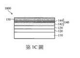
如第1C圖所示,在交替層140上形成至少一應力鬆弛層150。在一些實施例中,應力鬆弛層150可以是含鋁層,例如氮化鋁(AlN)、氮化鋁鎵(AlGaN)或前述之組合,並且應力鬆弛層150的厚度可以是在約0.1nm至約10nm的範圍,例如約1nm。應力鬆弛層150的形成可以包含沉積製程,例如有機金屬化學氣相沉積、分子束磊晶、液相磊晶或其他的沉積技術。As shown in FIG. 1C, at least one
如前所述,可以根據需求設置多對交替層140,然而,由於交替層140與基底110的熱膨脹係數不同,隨著交替層140的數量和厚度增加,產生的應力越大,導致曲度(bow)、裂痕與厚度不均的問題,這些問題限制了可以設置的交替層140數量。本案在交替層140上設置應力鬆弛層150,可以緩解設置交替層140的應力,因此可以增加交替層140的數量和厚度,使高電子遷移率電晶體裝置1000達到更高的耐壓程度。As mentioned above, multiple pairs of alternating
然後如第1D圖所示,根據一些實施例,在應力鬆弛層150上方形成氮化鎵層160。氮化鎵層160具有較佳晶體品質,可以提供用於形成其他元件的平坦表面。氮化鎵層160的形成可以包含沉積製程,例如有機金屬化學氣相沉積、分子束磊晶、液相磊晶或其他的沉積技術。可以根據需求選擇氮化鎵層160的厚度。在一些實施例中,氮化鎵層160的厚度在約10nm和約1μm的範圍,例如約0.5μm。Then, as shown in FIG. 1D, according to some embodiments, a
然後如第1E圖所示,在氮化鎵層160上方形成阻障層170。阻障層170的形成可以包含沉積製程,例如有機金屬化學氣相沉積、分子束磊晶、液相磊晶或其他的沉積技術。可以根據需求選擇阻障層170的厚度。在一些實施例中,阻障層170的材料可以包含第III族氮化物,例如III-V族化合物半導體材料。阻障層170可以包含單層或多層結構。舉例來說,阻障層170包含AlN、AlGaN、AlInN、AlGaInN、類似的材料或前述之組合。可以根據需求將阻障層170摻雜或不摻雜。選擇阻障層170的材料,以在氮化鎵層160和阻障層170之間的界面產生二維電子氣。Then, as shown in FIG. 1E, a
然後根據一些實施例,在阻障層170上方設置源極180、閘極190和汲極200,形成高電子遷移率電晶體裝置1000。可以使用任何合適的材料、製程和順序形成源極180、閘極190和汲極200,並且根據需求調整元件的間距和位置。在第1E圖繪示的實施例中,源極180、閘極190和汲極200位於阻障層170上,但本發明不限於此。Then, according to some embodiments, the
此外,可以根據需求設置應力鬆弛層150和交替層140的數量及配置。第2-4圖是根據一些其他實施例繪示高電子遷移率電晶體裝置的剖面示意圖。根據一些實施例,如第2圖所示,在高電子遷移率電晶體裝置2000中,在兩對交替層140之間設置應力鬆弛層150,隨後在交替層140上方設置接觸交替層140的氮化鎵層160。雖然並未繪示,根據一些實施例,可以在高電子遷移率電晶體裝置2000之交替層140和氮化鎵層160之間設置多對交替層140和多層應力鬆弛層150。這些應力鬆弛層150可以位於每一對交替層140上方,或者只位於特定的交替層140之間。根據需求,這些應力鬆弛層150可以具有相同或不同的厚度。In addition, the number and configuration of the
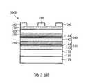
此外,根據另一些實施例,如第3圖所示,在高電子遷移率電晶體裝置3000中,分別在兩對交替層140上方設置兩層應力鬆弛層150,隨後在應力鬆弛層150上方設置接觸應力鬆弛層150的氮化鎵層160。雖然並未繪示,根據一些實施例,可以在高電子遷移率電晶體裝置3000之應力鬆弛層150和氮化鎵層160之間設置多對交替層140和多層應力鬆弛層150。這些應力鬆弛層150可以位於每一對交替層140上方,或者只位於特定的交替層140之間。根據需求,這些應力鬆弛層150可以具有相同或不同的厚度。In addition, according to other embodiments, as shown in FIG. 3, in the high electron
此外,根據又一些實施例,如第4圖所示,高電子遷移率電晶體裝置4000的緩衝層130可以包含漸變式緩衝層(gradient buffer layer)、超晶格緩衝層(superlattice buffer layer)、類似的緩衝層或前述之組合。雖然第4圖繪示緩衝層130包含超晶格緩衝層220和漸變式緩衝層230,但可以只使用超晶格緩衝層220或漸變式緩衝層230。In addition, according to other embodiments, as shown in FIG. 4, the
在一些實施例中,超晶格緩衝層220包含多組具有濃度差異的膜層,每組膜層包含多對氮化鋁層和氮化鋁鎵層。舉例來說,如第4圖所示,超晶格緩衝層220包含第一組包含氮化鋁鎵層222a和氮化鋁層222b的膜層、第二組包含氮化鋁鎵層224a和氮化鋁層224b的膜層、第三組包含氮化鋁鎵層226a和氮化鋁層226b的膜層,但本發明不限於此,超晶格緩衝層220可以包含更多組膜層及/或更多對氮化鋁層和氮化鋁鎵層。超晶格緩衝層220的形成可以包含沉積製程,例如有機金屬化學氣相沉積、分子束磊晶、液相磊晶或其他的沉積技術。根據需求,超晶格緩衝層220的每一對氮化鋁鎵層和氮化鋁層與其他對氮化鋁鎵層和氮化鋁層可以具有相同或不同的厚度和氮化鋁鎵層的鋁濃度。In some embodiments, the
在一些實施例中,漸變式緩衝層230包含多層具有濃度差異的氮化鋁鎵層。舉例來說,如第4圖所示,漸變式緩衝層230包含三層氮化鋁鎵層232、234、236,但本發明不限於此,可以設置更多或更少層氮化鋁鎵層。漸變式緩衝層230的形成可以包含沉積製程,例如有機金屬化學氣相沉積、分子束磊晶、液相磊晶或其他的沉積技術。根據需求,漸變式緩衝層230的每層氮化鋁鎵層可以各自具有相同或不同的厚度和鋁濃度。In some embodiments, the graded
如第4圖所示,設置包含超晶格緩衝層220和漸變式緩衝層230的緩衝層130,可以減緩在緩衝層130上方設置的交替層140的應力,避免產生裂縫,因此可增加交替層140的厚度。此外,在相同厚度下,相較於只形成超晶格緩衝層220,形成包含超晶格緩衝層220和漸變式緩衝層230的緩衝層130可大幅縮短成長時間。另外,相較於只形成漸變式緩衝層230,形成包含超晶格緩衝層220和漸變式緩衝層230的緩衝層130可以在上方形成的交替層140具有較佳的結晶品質。因此可以在提高產能的同時,提升高電子遷移率電晶體裝置的效能和良率。As shown in Figure 4, the provision of a
隨後參照前述的方法、材料和配置,在漸變式緩衝層230上方設置多對交替層140和至少一層應力鬆弛層150,然後設置氮化鎵層160。然後設置阻障層170、源極180、閘極190和汲極200,形成高電子遷移率電晶體裝置4000。Subsequently, referring to the aforementioned methods, materials, and configurations, multiple pairs of alternating
綜上所述,根據本發明的一些實施例,在摻雜碳的氮化鎵層上方設置未摻雜的氮化鎵層,可以改善摻雜碳的氮化鎵層的晶體品質和表面粗糙度。因此,可以保持高電子遷移率電晶體裝置的性能,例如二維電子氣特性,進一步提升裝置耐壓程度。In summary, according to some embodiments of the present invention, disposing an undoped gallium nitride layer above the carbon-doped gallium nitride layer can improve the crystal quality and surface roughness of the carbon-doped gallium nitride layer . Therefore, the performance of the high electron mobility transistor device can be maintained, such as the two-dimensional electron gas characteristics, and the voltage resistance of the device can be further improved.
此外,根據本發明的一些實施例,在包含摻雜碳的氮化鎵層和未摻雜的氮化鎵層的交替層上方設置應力鬆弛層,可以緩解設置交替層的應力,因此可以增加交替層的數量和厚度,使高電子遷移率電晶體裝置達到更高的耐壓程度。In addition, according to some embodiments of the present invention, disposing a stress relaxation layer on the alternating layer containing the carbon-doped gallium nitride layer and the undoped gallium nitride layer can alleviate the stress of disposing the alternating layer, so the alternating layer can be increased. The number and thickness of the layers enable the high electron mobility transistor device to achieve a higher degree of withstand voltage.
另外,根據本發明的一些實施例,在基底上方設置包含漸變式緩衝層和超晶格緩衝層的緩衝層,可以減緩在緩衝層上方設置的交替層的應力,避免產生裂縫或翹曲,因此可增加交替層的厚度。此外,相較於只形成超晶格緩衝層或漸變式緩衝層,包含漸變式緩衝層和超晶格緩衝層的緩衝層可以在提高產能的同時,提升高電子遷移率電晶體裝置的效能和良率。In addition, according to some embodiments of the present invention, a buffer layer including a graded buffer layer and a superlattice buffer layer is provided above the substrate, which can reduce the stress of the alternating layers provided above the buffer layer and avoid cracks or warpage. The thickness of the alternating layers can be increased. In addition, compared to only forming a superlattice buffer layer or a graded buffer layer, a buffer layer including a graded buffer layer and a superlattice buffer layer can increase productivity while increasing the performance of high electron mobility transistor devices.Efficiency and yield.
雖然本發明已以多個實施例描述如上,但這些實施例並非用於限定本發明。本發明所屬技術領域中具有通常知識者應可理解,他們能以本發明實施例為基礎,做各式各樣的改變、取代和替換,以達到與在此描述的多個實施例相同的目的及/或優點。本發明所屬技術領域中具有通常知識者也可理解,此類修改或設計並未悖離本發明的精神和範圍。因此,本發明之保護範圍當視後附的申請專利範圍所界定者為準。Although the present invention has been described above in terms of multiple embodiments, these embodiments are not intended to limit the present invention. Those with ordinary knowledge in the technical field to which the present invention belongs should understand that they can make various changes, substitutions and substitutions based on the embodiments of the present invention to achieve the same purpose as the multiple embodiments described herein. And/or advantages. Those with ordinary knowledge in the technical field to which the present invention belongs can also understand that such modifications or designs do not depart from the spirit and scope of the present invention. Therefore, the scope of protection of the present invention shall be subject to those defined by the attached patent scope.
110‧‧‧基底110‧‧‧Base
120‧‧‧成核層120‧‧‧nucleation layer
130‧‧‧緩衝層130‧‧‧Buffer layer
140‧‧‧交替層140‧‧‧Alternating layer
142‧‧‧摻雜碳的氮化鎵層142‧‧‧Carbon-doped gallium nitride layer
144‧‧‧未摻雜的氮化鎵層144‧‧‧Undoped GaN layer
150‧‧‧應力鬆弛層150‧‧‧Stress relaxation layer
160‧‧‧氮化鎵層160‧‧‧Gallium Nitride Layer
170‧‧‧阻障層170‧‧‧Barrier layer
180‧‧‧源極180‧‧‧Source
190‧‧‧閘極190‧‧‧Gate
200‧‧‧汲極200‧‧‧Dip pole
1000‧‧‧高電子遷移率電晶體裝置1000‧‧‧High Electron Mobility Transistor Device
Claims (20)
Translated fromChinesePriority Applications (1)
| Application Number | Priority Date | Filing Date | Title |
|---|---|---|---|
| TW107137949ATWI713221B (en) | 2018-10-26 | 2018-10-26 | High electron mobility transistor and methods for forming the same |
Applications Claiming Priority (1)
| Application Number | Priority Date | Filing Date | Title |
|---|---|---|---|
| TW107137949ATWI713221B (en) | 2018-10-26 | 2018-10-26 | High electron mobility transistor and methods for forming the same |
Publications (2)
| Publication Number | Publication Date |
|---|---|
| TW202017187A TW202017187A (en) | 2020-05-01 |
| TWI713221Btrue TWI713221B (en) | 2020-12-11 |
Family
ID=71895643
Family Applications (1)
| Application Number | Title | Priority Date | Filing Date |
|---|---|---|---|
| TW107137949ATWI713221B (en) | 2018-10-26 | 2018-10-26 | High electron mobility transistor and methods for forming the same |
Country Status (1)
| Country | Link |
|---|---|
| TW (1) | TWI713221B (en) |
Families Citing this family (4)
| Publication number | Priority date | Publication date | Assignee | Title |
|---|---|---|---|---|
| TWI768985B (en)* | 2021-06-25 | 2022-06-21 | 世界先進積體電路股份有限公司 | Semiconductor structure and high electron mobility transistor |
| US11942519B2 (en) | 2021-09-01 | 2024-03-26 | Vanguard International Semiconductor Corporation | Semiconductor structure and high electron mobility transistor |
| TW202406146A (en) | 2022-07-27 | 2024-02-01 | 聯華電子股份有限公司 | High electron mobility transistor and method for fabricating the same |
| TWI857470B (en)* | 2022-11-18 | 2024-10-01 | 環球晶圓股份有限公司 | Epitaxial structure |
Citations (1)
| Publication number | Priority date | Publication date | Assignee | Title |
|---|---|---|---|---|
| US20170294529A1 (en)* | 2016-04-11 | 2017-10-12 | Qorvo Us, Inc. | High electron mobility transistor (hemt) device |
- 2018
- 2018-10-26TWTW107137949Apatent/TWI713221B/enactive
Patent Citations (1)
| Publication number | Priority date | Publication date | Assignee | Title |
|---|---|---|---|---|
| US20170294529A1 (en)* | 2016-04-11 | 2017-10-12 | Qorvo Us, Inc. | High electron mobility transistor (hemt) device |
Also Published As
| Publication number | Publication date |
|---|---|
| TW202017187A (en) | 2020-05-01 |
Similar Documents
| Publication | Publication Date | Title |
|---|---|---|
| US11114555B2 (en) | High electron mobility transistor device and methods for forming the same | |
| TWI713221B (en) | High electron mobility transistor and methods for forming the same | |
| JP5309452B2 (en) | Semiconductor wafer, semiconductor device, and manufacturing method | |
| JP5503487B2 (en) | III-V semiconductor device having strain buffering interlayer | |
| US9233844B2 (en) | Graded aluminum—gallium—nitride and superlattice buffer layer for III-V nitride layer on silicon substrate | |
| US20210057561A1 (en) | High electron mobility transistor device and methods for forming the same | |
| CN112242435B (en) | Semiconductor epitaxial structure and method for forming the same | |
| US20170092751A1 (en) | Heterojunction field-effect transistor | |
| TWI678723B (en) | High electron mobility transistor and methods for forming the same | |
| WO2018092689A1 (en) | Compound semiconductor substrate manufacturing method and compound semiconductor substrate | |
| JP5824814B2 (en) | Semiconductor wafer, semiconductor element, and manufacturing method thereof | |
| JP5379391B2 (en) | Semiconductor device comprising gallium nitride compound semiconductor and method for manufacturing the same | |
| CN111146282B (en) | High electron mobility transistor device and method of manufacturing the same | |
| JP2012049170A (en) | Nitride semiconductor device | |
| JP2015103665A (en) | Nitride semiconductor epitaxial wafer and nitride semiconductor | |
| JP7629054B2 (en) | High electron mobility transistor epitaxial construction | |
| CN111146269A (en) | High electron mobility transistor device and method of manufacturing the same | |
| CN106783968B (en) | Semiconductor device including buffer layer of gallium aluminum nitride and gallium indium nitride and method of manufacturing the same | |
| TW202324748A (en) | High electron mobility transistor device | |
| WO2022014592A1 (en) | Compound semiconductor substrate and method for manufacturing compound semiconductor substrate | |
| CN114080692A (en) | Group III nitride-based semiconductor wafer | |
| JP6264485B2 (en) | Compound semiconductor device and manufacturing method thereof | |
| JP2007329154A (en) | Method of manufacturing nitride semiconductor device | |
| KR20200074895A (en) | Manufacturing method of power transistor and power transistor manufactured according to the manufacturing method | |
| US20230299146A1 (en) | Semiconductor structures |