TWI713209B - Optical sensor and method for forming the same - Google Patents
Optical sensor and method for forming the sameDownload PDFInfo
- Publication number
- TWI713209B TWI713209BTW107133793ATW107133793ATWI713209BTW I713209 BTWI713209 BTW I713209BTW 107133793 ATW107133793 ATW 107133793ATW 107133793 ATW107133793 ATW 107133793ATW I713209 BTWI713209 BTW I713209B
- Authority
- TW
- Taiwan
- Prior art keywords
- light
- transmitting
- layer
- optical sensor
- pillars
- Prior art date
Links
- 230000003287optical effectEffects0.000titleclaimsabstract22
- 239000000758substrateSubstances0.000claimsabstract12
- 239000000463materialSubstances0.000claims4
- 230000002093peripheral effectEffects0.000claims2
Images


Landscapes
- Solid State Image Pick-Up Elements (AREA)
Abstract
Description
Translated fromChinese本發明係有關於一種光學元件,特別是有關於一種光學感應器及其形成方法。The present invention relates to an optical element, in particular to an optical sensor and its forming method.
光學感應器中的光學元件可包括光準直器(light collimator)、分束器、聚焦鏡以及線性感測器。其中,光準直器的功能在於準直光線,以減少因光發散所導致之能量損失。舉例而言,光準直器可被應用於光學感應器中,以增加指紋辨識裝置的效能。The optical elements in the optical sensor may include a light collimator, a beam splitter, a focusing lens, and a linear sensor. Among them, the function of the light collimator is to collimate light to reduce the energy loss caused by light divergence. For example, an optical collimator can be used in an optical sensor to increase the performance of the fingerprint recognition device.
光準直器包括透光柱及包圍透光柱的遮光層,以達到準直光線的效果。因設計需求,需要高高寬比(aspect ratio)之透光柱時,可能因製程能力限制而容易使透光柱倒塌變形,影響光準直器之準直效果,進一步影響光學感應器的良率。The light collimator includes a light transmitting rod and a light shielding layer surrounding the light transmitting rod to achieve the effect of collimating light. Due to design requirements, when a high-aspect ratio light-transmitting column is required, the light-transmitting column may collapse and deform due to the limitation of the manufacturing process, which affects the collimation effect of the light collimator and further affects the quality of the optical sensor. rate.
雖然現有的光學感應器大致符合需求,但並非各方面皆令人滿意,特別是提高光學感應器的光準直器透光柱之高寬比仍需進一步改善。Although the existing optical sensor generally meets the requirements, it is not satisfactory in all aspects. In particular, the height-to-width ratio of the light-transmitting column of the optical collimator of the optical sensor still needs to be further improved.
根據一實施例,本發明提供一種光學感應器,包括:畫素,位於基板中;光準直層,位於基板之上,包括:透光層,毯覆性地位於基板之上,覆蓋畫素與畫素之間的區域; 遮光層,位於透光層上方;以及透光柱,穿過遮光層,對應設置於畫素上。According to an embodiment, the present invention provides an optical sensor, including: pixels located in a substrate; a light collimation layer located on the substrate, including: a light-transmitting layer, blanketed on the substrate, covering the pixels The area between the pixel and the pixel; the light-shielding layer, located above the light-transmitting layer; and the light-transmitting column, which passes through the light-shielding layer, and is correspondingly disposed on the pixel.
根據另一實施例,本發明提供一種光學感應器的形成方法,包括:形成畫素於基板中;形成光準直層於基板之上,其中光準直層的形成包括:毯覆性地形成透光層於基板之上,覆蓋畫素與畫素之間的區域;形成透光柱於透光層之上,其中透光柱對應設置於畫素上;形成遮光層於透光柱之間;以及平坦化透光柱與遮光層的上表面。According to another embodiment, the present invention provides a method for forming an optical sensor, including: forming pixels in a substrate; forming a light collimating layer on the substrate, wherein the forming of the light collimating layer includes: blanket forming The light-transmitting layer is on the substrate, covering the area between the pixels; forming light-transmitting pillars on the light-transmitting layer, wherein the light-transmitting pillars are correspondingly arranged on the pixels; forming a light-shielding layer between the light-transmitting pillars ; And planarizing the upper surface of the light-transmitting column and the light-shielding layer.
為讓本發明之上述目的、特徵及優點能更明顯易懂,下文特舉數個實施例,並配合所附圖式,作詳細說明如下。In order to make the above-mentioned objects, features and advantages of the present invention more obvious and understandable, several embodiments are cited below in conjunction with the accompanying drawings, which are described in detail as follows.
100、200、300、400、500、600‧‧‧光學感應器100, 200, 300, 400, 500, 600‧‧‧Optical sensor
102‧‧‧基板102‧‧‧Substrate
104‧‧‧畫素104‧‧‧Pixel
106‧‧‧透光層106‧‧‧Transparent layer
108、208、308、408‧‧‧透光柱108, 208, 308, 408‧‧‧light transmission column
110‧‧‧遮光層110‧‧‧Shading layer
112、612‧‧‧光準直層112, 612‧‧‧Optical collimation layer
514‧‧‧底遮光層514‧‧‧Bottom shading layer
608D‧‧‧虛置透光柱608D‧‧‧Dummy light column
HL、HP‧‧‧高度HL, HP‧‧‧Height
θ1、θ2、θ3‧‧‧夾角θ1, θ2, θ3‧‧‧Included angle
以下將配合所附圖式詳述本發明實施例。應注意的是,依據在業界的標準做法,各種特徵並未按照比例繪製且僅用以說明例示。事實上,可能任意地放大或縮小元件的尺寸,以清楚地表現出本發明實施例的特徵。The embodiments of the present invention will be described in detail below in conjunction with the accompanying drawings. It should be noted that, according to standard practices in the industry, various features are not drawn to scale and are only used for illustration and illustration. In fact, it is possible to arbitrarily enlarge or reduce the size of the element to clearly show the characteristics of the embodiment of the present invention.
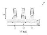
第1至4圖係根據一些實施例繪示出形成光學感應器不同階段的剖面示意圖。FIGS. 1 to 4 are schematic cross-sectional views illustrating different stages of forming an optical sensor according to some embodiments.
第5圖係根據另一些實施例繪示出光學感應器的剖面圖。FIG. 5 is a cross-sectional view of the optical sensor according to other embodiments.
第6圖係根據又一些實施例繪示出光學感應器的剖面圖。Fig. 6 is a cross-sectional view of an optical sensor according to still other embodiments.
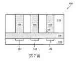
第7圖係根據再一些實施例繪示出光學感應器的剖面圖。FIG. 7 is a cross-sectional view of the optical sensor according to still other embodiments.
第8圖係根據其他一些實施例繪示出光學感應器的剖面 圖。Figure 8 is a cross-sectional view of the optical sensor according to some other embodiments.
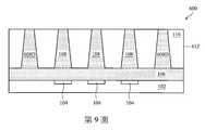
第9圖係根據其他一些實施例繪示出光學感應器的剖面圖。FIG. 9 is a cross-sectional view of the optical sensor according to some other embodiments.
以下公開許多不同的實施方法或是例子來實行本發明實施例之不同特徵,以下描述具體的元件及其排列的實施例以闡述本發明實施例。當然這些實施例僅用以例示,且不該以此限定本發明實施例的範圍。例如,在說明書中提到第一特徵形成於第二特徵之上,其包括第一特徵與第二特徵是直接接觸的實施例,另外也包括於第一特徵與第二特徵之間另外有其他特徵的實施例,亦即,第一特徵與第二特徵並非直接接觸。此外,在不同實施例中可能使用重複的標號或標示,這些重複僅為了簡單清楚地敘述本發明實施例,不代表所討論的不同實施例及/或結構之間有特定的關係。Many different implementation methods or examples are disclosed below to implement different features of the embodiments of the present invention. The following describes specific elements and their arrangement embodiments to illustrate the embodiments of the present invention. Of course, these embodiments are only for illustration, and should not be used to limit the scope of the embodiments of the present invention. For example, in the specification, it is mentioned that the first feature is formed on the second feature, which includes the embodiment in which the first feature and the second feature are in direct contact, and also includes the embodiments between the first feature and the second feature. The embodiment of the feature, that is, the first feature and the second feature are not in direct contact. In addition, repeated reference numerals or labels may be used in different embodiments, and these repetitions are only used to briefly and clearly describe the embodiments of the present invention, and do not represent a specific relationship between the different embodiments and/or structures discussed.
此外,其中可能用到與空間相對用詞,例如「在...下方」、「下方」、「較低的」、「上方」、「較高的」及類似的用詞,這些空間相對用詞係為了便於描述圖示中一個(些)元件或特徵與另一個(些)元件或特徵之間的關係,這些空間相對用詞包括使用中或操作中的裝置之不同方位,以及圖式中所描述的方位。當裝置被轉向不同方位時(旋轉90度或其他方位),則其中所使用的空間相對形容詞也將依轉向後的方位來解釋。In addition, terms that are relative to space may be used, such as "below", "below", "lower", "above", "higher" and similar terms. These spaces are relatively used In order to facilitate the description of the relationship between one element(s) or feature and another element(s) or feature in the illustration, these spatially relative terms include the different orientations of the device in use or operation, and the The orientation described. When the device is turned in different directions (rotated by 90 degrees or other directions), the spatially relative adjectives used therein will also be interpreted according to the turned position.
在此,「約」、「大約」、「大抵」之用語通常表示在一給定值或範圍的20%之內,較佳是10%之內,且更佳是5%之內,或3%之內,或2%之內,或1%之內,或0.5%之內。應注意 的是,說明書中所提供的數量為大約的數量,亦即在沒有特定說明「約」、「大約」、「大抵」的情況下,仍可隱含「約」、「大約」、「大抵」之含義。Here, the terms "about", "approximately", and "approximately" usually mean within 20% of a given value or range, preferably within 10%, and more preferably within 5%, or 3 Within %, or within 2%, or within 1%, or within 0.5%. It should be noted that the quantity provided in the manual is an approximate quantity, that is, without specific description of "about", "approximately", "approximately", "about", "approximately" and "approximately" can still be implied. The meaning of "probably".
雖然所述的一些實施例中的步驟以特定順序進行,這些步驟亦可以其他合邏輯的順序進行。在不同實施例中,可替換或省略一些所述的步驟,亦可於本發明實施例所述的步驟之前、之中、及/或之後進行一些其他操作。本發明實施例中的光學感應器可加入其他的特徵。在不同實施例中,可替換或省略一些特徵。Although the steps in some of the described embodiments are performed in a specific order, these steps can also be performed in other logical orders. In different embodiments, some of the steps described may be replaced or omitted, and some other operations may be performed before, during, and/or after the steps described in the embodiments of the present invention. Other features can be added to the optical sensor in the embodiment of the present invention. In different embodiments, some features may be replaced or omitted.
本發明實施例提供一種光學感應器,藉由在透光柱陣列下方與畫素之間毯覆性地(blanketly)設置透光層,可避免製程能力限制,提高透光部分的總高寬比,並可依製程需求改變透光柱在剖面圖的形狀大小,使光線垂直入射透光層,可避免光線逸散,提升製程良率。The embodiment of the present invention provides an optical sensor. By blanketly disposing a light-transmitting layer under the light-transmitting column array and between the pixels, it can avoid the limitation of process capability and increase the total aspect ratio of the light-transmitting part And the shape and size of the light-transmitting column in the cross-sectional view can be changed according to the process requirements, so that the light enters the light-transmitting layer perpendicularly, which can prevent the light from escaping and improve the process yield.
第1至4圖係根據一些實施例繪示出形成光學感應器100不同階段的剖面示意圖。如第1圖所示,提供一基板102。此基板102可為半導體基板,例如矽基板。此外,上述半導體基板亦可為元素半導體,包括鍺(germanium);化合物半導體,包括氮化鎵(gallium nitride,GaN)、碳化矽(silicon carbide)、砷化鎵(gallium arsenide)、磷化鎵(gallium phosphide)、磷化銦(indium phosphide)、砷化銦(indium arsenide)及/或銻化銦(indium antimonide);合金半導體,包括矽鍺合金(SiGe)、磷砷鎵合金(GaAsP)、砷鋁銦合金(AlInAs)、砷鋁鎵合金(AlGaAs)、砷銦鎵合金(GaInAs)、磷銦鎵合金(GaInP)、及/或磷砷銦鎵合 金(GaInAsP)、或上述材料之組合。在一些實施例中,基板102也可以是絕緣層上覆半導體(semiconductor on insulator,SOI)基板,上述絕緣層覆半導體基板可包括底板、設置於底板上之埋藏氧化層、或設置於埋藏氧化層上之半導體層。此外,基板102可為N型或P型導電型。1 to 4 are schematic cross-sectional diagrams illustrating different stages of forming the
在一些實施例中,基板102可包括各種隔離部件(未繪示),用以定義主動區,並電性隔離基板102之中/之上的主動區元件。在一些實施例中,隔離部件包括淺溝槽隔離(shallow trench isolation,STI)部件、局部矽氧化(local oxidation of silicon,LOCOS)部件、其他合適的隔離部件、或上述之組合。在一些實施例中,形成隔離部件可例如包括形成絕緣層於基板102之上,選擇性蝕刻絕緣層及基板102以於基板102中形成溝槽,於溝槽中成長富含氮(例如氮氧化矽)的襯層,以沉積製程於溝槽中填入絕緣材料(例如二氧化矽、氮化矽、或氮氧化矽),對溝槽中絕緣材料進行退火製程,並以例如化學機械研磨(Chemical mechanical polishing,CMP)製程對基板102進行平坦化製程,以去除多餘的絕緣材料,使溝槽中的絕緣材料與基板102的頂表面等高。In some embodiments, the
在一些實施例中,基板102可包括各種以如離子佈植及/或擴散製程所形成之P型摻雜區及/或N型摻雜區(未繪示)。在一些實施例中,摻雜區可形成電晶體、光二極體等元件。然而,上述之元件僅為範例,本發明並不以此為限。In some embodiments, the
在一些實施例中,基板102可包括各種導電部件(例如:導線或導孔)(未繪示)。例如,上述導電特徵可由鋁(Al)、銅 (Cu)、鎢(W)、其他適當之導電材料、上述之合金、或上述之組合所形成。In some embodiments, the
如第1圖所示,在一些實施例中,基板102中可包括畫素104。畫素104可包括光感測器。光感測器可包括光二極體、電荷耦合元件(charged coupling device,CCD)感測器、互補式金屬氧化物半導體(complimentary metal-oxide-semiconductor,CMOS)影像感測器、主動感測器、被動感測器、其他適合的感測器、或上述之組合。在一些實施例中,一個畫素104可對應至至少一個光感測器,例如至少一個光二極體。此外,光感測器可連接至讀出電路(read out circuit)(未繪示)。讀出電路可包括傳輸電晶體(transfer transistor)、重置電晶體(reset transistor)、源極隨耦電晶體(source-follower transistor)、選擇電晶體(select transistor)、一或多種其他合適的電晶體、或上述之組合。畫素104可藉由光感測器將接收到的光訊號轉換成電子訊號,並透過讀出電路讀取上述電子訊號。值得注意的是,在第1圖中僅繪示出部分畫素104,實際上的數量並不以此為限。在一些實施例中,畫素104以陣列方式排列在基板中。As shown in FIG. 1, in some embodiments, the
接著,如第2圖所繪示,在基板102上毯覆性地(blanketly)形成透光層106。在一些實施例中,透光層106可包括透光材料,其對於波長300nm至1100nm光線的透光度大於60%。透光材料可包括光固化材料、熱固化材料、或上述之組合。在一些實施例中,透光材料可包括例如聚甲基丙烯酸甲酯(poly(methyl methacrylate,PMMA)、全氟環丁基 (perfluorocyclobutyl,PFCB)聚合物、聚亞醯胺、環氧樹脂、其他適當之材料、或上述之組合。在一些實施例中,可以旋轉塗佈法(spin coating)、化學氣相沉積法、鑄模(casting)、棒狀塗佈(roller coating)、刮刀塗佈(blade coating)、線棒塗佈(wire bar coating)、浸漬塗佈(dip coating)、其他適當之方法、或上述之組合於基板102上沉積透光材料。Next, as shown in FIG. 2, a light-transmitting
在一些實施例中,透光層106的高度HL介於30μm至500μm之間。透光層106的高度HL若太高,則上方入射的光線容易逸散至畫素104之外的區域。透光層106的高度HL若太低,則不易使後續形成的整體透光部分具高高寬比(aspect ratio)。In some embodiments, the height HL of the light-transmitting
接著,如第3圖所繪示,在透光層106上形成透光柱108。在一些實施例中,可先於透光層106上毯覆性地形成透光材料(圖未示)。在一些實施例中,用以形成透光柱108的材料可與前述形成透光層106的材料相同或相似,此處不重述。在另一些實施例中,透光柱108與透光層106的材料不同,視製程需求而定。在第3圖中,由於透光柱108與透光層106使用相同的透光材料,兩者之間可能沒有明顯的界面,其交界處以虛線表示。Next, as shown in FIG. 3, a light-transmitting
接著,選擇性地去除透光層106上的透光材料。在一些實施例中,透光材料若非光阻材料,可以微影製程及蝕刻製程選擇性去除透光材料以在畫素104上方的透光層106上對應形成透光柱108。在一些實施例中,微影製程可包括光阻塗佈(例如旋轉塗佈)、軟烤(soft baking)、罩幕對準、曝光圖案、曝光後烘烤(post-exposure baking)、光阻顯影、清洗及乾燥(例 如硬烤(hard baking))、其他合適的技術、或上述之組合。蝕刻製程可包括乾蝕刻製程(例如反應離子蝕刻(reactive ion etch,RIE)、電漿蝕刻、離子研磨(ion milling))、濕蝕刻製程、或上述之組合。在另一些實施例中,透光材料為光阻材料,可藉由固化製程如光固化製程固化透光材料並清洗未曝光的部分而直接形成透光柱108。可藉由透過圖案化製程中曝光的焦距而改變透光柱108在剖面圖中的形狀。例如,如第3圖所示,透光柱108在剖面圖中為上窄下寬的梯形。在一些其他實施例中,透光柱108在剖面圖中亦可為其他形狀,例如上寬下窄的倒梯形、矩形、非線性(non-linear)側壁之圖案、其他合適的形狀、或上述之組合。Next, the light-transmitting material on the light-transmitting
在一些實施例中,透光柱108的高度HP介於30μm至500μm之間。透光柱108的高度HP若太高,則容易變形倒塌。透光柱108的高度HP若太低,則不足以使上方光線垂直入射於透光層106,而使光線逸散至畫素104之外的區域。In some embodiments, the height HP of the light-transmitting
接著,如第4圖所繪示,在透光層106上方之透光柱108之間形成遮光層110。在一些實施例中,遮光層110可包括遮光材料,其對於波長350nm至1100nm光線的吸收度大於90%。上述遮光材料可包括光固化材料、熱固化材料、或上述之組合。在一些實施例中,遮光材料包括非透明的光阻、油墨、模制化合物(molding compound)、防焊材料(solder mask)、其他適當之材料、或上述之組合。在一些實施例中,可將遮光材料設置於透光層106上方之透光柱108之間,並進行固化製程如光固化製程、熱固化製程或上述之組合以固化遮光材料並形成 遮光層110。在一些實施例中,使用單一遮光材料形成遮光層110,如此一來,可簡化製程,降低量產時間及成本。Then, as shown in FIG. 4, a
接著,以例如化學機械研磨製程對透光柱108及遮光層110進行平坦化製程,以去除多餘的遮光材料,使透光柱108及遮光層110之頂表面等高。如此,便形成包括透光層106、透光柱108、及遮光層110的光準直層112。Then, a planarization process is performed on the light-transmitting
如第4圖所示,藉由分別形成透光層106及透光柱108,可提高光準直層112中透光部分的高寬比(aspect ratio),避免於單次製程中因透光柱108太高而使其變形倒塌。例如,在一些實施例中,透光柱108的高度HP及透光層106的高度HL的總和與透光柱108的平均寬度的比值介於1:1至50:1之間。As shown in Figure 4, by separately forming the light-transmitting
在一些實施例中,可調整透光柱108在剖面圖的形狀與高度,使入射光由上方垂直入射透光層106。如此一來,可避免入射的光線逸散至畫素104之外的區域。In some embodiments, the shape and height of the cross-sectional view of the light-transmitting
在一些實施例中,透光柱108直徑與透光層106的高度比值介於1至50之間。透光柱108直徑與透光層106的高度比值若太大,則容易因透光柱108太高而使其變形倒塌。透光柱108直徑與透光層106的高度比值若太小,則由上方入射的光線容易逸散至畫素104之外的區域。In some embodiments, the ratio of the diameter of the light-transmitting
此外,在一些實施例中,如第4圖所示,透光柱108在剖面圖中為大小相同之上窄下寬的梯形,其底面積大於頂面積。如此一來,可使遮光層110較易形成於透光柱108之間,避免於透光柱108與遮光層110之間形成空隙,影響準直效果。In addition, in some embodiments, as shown in FIG. 4, the light-transmitting
在一些實施例中,透光柱108的側壁與其底表面的 夾角θ1為30°至89°之間。夾角θ1若太大,則可能因不易填入遮光層110而降低準直效果。夾角θ1若太小,則可能因透光的面積太小而減少其下方畫素104吸收的光量。In some embodiments, the angle θ1 between the sidewall of the light-transmitting
在一些實施例中,光準直層112上方可包括其他光學元件例如彩色濾光片、玻璃、微透鏡等(未繪示)。入射的光線透過光準直層112上方的光學元件經過透光柱108及透光層106照射畫素104。在一些實施例中,透光柱108位於畫素104之正上方。如此一來,可增加照射畫素104的光量。In some embodiments, other optical elements such as color filters, glass, micro lenses, etc. (not shown) may be included above the
如上所述,藉由分別形成光學感應器之光準直層的透光部分,可提高透光部分的總高寬比,避免透光柱太高而變形倒塌,並藉由調整各層透光柱在剖面圖的形狀及大小,可使上方入射光垂直入射透光層,避免光線逸散至畫素之外的區域。又例如使各層透光柱的底面積大於其頂面積,可使遮光層較易形成於透光柱之間,避免於透光柱與遮光層之間形成空隙,進而改善準直效果,提升良率。As mentioned above, by separately forming the light-transmitting parts of the light-collimating layer of the optical sensor, the total aspect ratio of the light-transmitting parts can be increased, and the light-transmitting pillars are prevented from being too high and deformed and collapsed, and by adjusting the light-transmitting pillars of each layer The shape and size of the cross-sectional view can make the upper incident light enter the light-transmitting layer perpendicularly, and prevent the light from escaping to the area outside the pixel. For another example, making the bottom area of each layer of light-transmitting pillars larger than its top area can make it easier for the light-shielding layer to be formed between the light-transmitting pillars and avoid the formation of gaps between the light-transmitting pillars and the light-shielding layer, thereby improving the collimation effect and improving rate.
第5圖係根據另一些實施例繪示出光學感應器200的剖面圖。其中與前述實施例相同或相似的製程或元件將沿用相同的元件符號,其詳細內容將不再贅述。與前述實施例的差別在於,如第5圖所示,透光柱208為上寬下窄的倒梯形。藉由分別形成透光柱208及透光層106,可避免於單次製程中因透光柱208太高而使其變形倒塌。在一些實施例中,可藉由透過圖案化製程中曝光的焦距而改變透光柱208在剖面圖中的形狀與高度,使入射光由上方垂直入射透光層106。如此一來,可避免入射的光線容易逸散至畫素104之外的區域。透光柱208為上 寬下窄的倒梯形,可增加製程良率。FIG. 5 is a cross-sectional view of the
在一些實施例中,透光柱208的側壁與其底表面的夾角θ2為90°至150°之間。夾角θ2若太大,則可能因透光的面積太小而減少其下方畫素104吸收的光量。夾角θ1若太小,則可能不易填入遮光層110而降低準直效果。In some embodiments, the angle θ2 between the sidewall of the light-transmitting
如第5圖所示的實施例中,藉由分別形成光學感應器之光準直層的透光部分,可提高透光部分的總高寬比,避免透光柱太高而變形倒塌,並藉由調整各層透光柱在剖面圖的形狀及大小,可使上方入射光垂直入射透光層,避免光線逸散至畫素之外的區域,進而改善準直效果,提升良率。As in the embodiment shown in Fig. 5, by separately forming the light-transmitting parts of the light-collimating layer of the optical sensor, the total aspect ratio of the light-transmitting parts can be increased, and the light-transmitting pillars can be prevented from being too high and deformed and collapsed. By adjusting the shape and size of the cross-sectional view of each layer of the light-transmitting rod, the upper incident light can be perpendicular to the light-transmitting layer, avoiding the light from escaping to the area outside the pixels, thereby improving the collimation effect and increasing the yield.
第6圖係根據另一些實施例繪示出光學感應器300的剖面圖。其中與前述實施例相同或相似的製程或元件將沿用相同的元件符號,其詳細內容將不再贅述。與前述實施例的差別在於,如第6圖所示,透光柱308具有非線性(non-linear)側壁。舉例而言,透光柱308為在剖面圖中為雙凹形(double concave)。藉由分別形成透光柱308及透光層106,可避免於單次製程中因透光柱308太高而使其變形倒塌。在一些實施例中,可藉由透過圖案化製程中曝光的焦距而改變透光柱308在剖面圖中的形狀與高度,使入射光由上方垂直入射透光層106。如此一來,可避免入射的光線容易逸散至畫素104之外的區域。透光柱308具有非線性側壁,可增加調變入射光線的自由度。FIG. 6 is a cross-sectional view of the
值得注意的是,第6圖中透光柱308在剖面圖中形狀僅為一範例,本發明並不以此為限。例如,透光柱308的非線性側壁可為拋物面(hyperbolic surface)、曲面(curvature surface)、半球狀面(half-sphere-like surface)、縮頸面(necking surface)、切口面(notching surface)、刻面(facet surface)、其他非線性面、或上述之組合,視製程及設計需求而定。It should be noted that the cross-sectional shape of the light-transmitting
如第6圖所示的實施例中,藉由分別形成光學感應器之光準直層的透光部分,可提高透光部分的總高寬比,避免透光柱太高而變形倒塌,並藉由調整各層透光柱在剖面圖的形狀及大小,可使入射光垂直入射透光層,避免光線逸散至畫素之外的區域。又例如使透光柱具有非線性側壁,可增加調變入射光線的自由度,進而改善準直效果,提升良率。As in the embodiment shown in Figure 6, by separately forming the light-transmitting parts of the light collimating layer of the optical sensor, the total aspect ratio of the light-transmitting parts can be increased, and the light-transmitting rods can be prevented from being too high and deformed and collapsed. By adjusting the shape and size of the cross-sectional view of the light-transmitting rods of each layer, the incident light can be perpendicular to the light-transmitting layer, and the light can be prevented from escaping to areas outside the pixels. For another example, making the light-transmitting rods have non-linear sidewalls can increase the freedom of modulating incident light, thereby improving the collimation effect and increasing the yield.
第7圖係根據另一些實施例繪示出光學感應器400的剖面圖。其中與前述實施例相同或相似的製程或元件將沿用相同的元件符號,其詳細內容將不再贅述。與前述實施例的差別在於,如第7圖所示,透光柱408在剖面圖中為矩形。在一些實施例中,可藉由透過圖案化製程中曝光的焦距而改變透光柱408在剖面圖中的形狀與高度,使入射光由上方垂直入射透光層106。如此一來,可避免入射的光線容易逸散至畫素104之外的區域。FIG. 7 is a cross-sectional view of the
在一些實施例中,透光柱408的側壁與其底表面的夾角θ3為90°。亦即,透光柱408的側壁與其底表面垂直。並且,透光柱408之底面積等於其頂面積。如此一來,可增加下方畫素104吸收的光量。In some embodiments, the angle θ3 between the sidewall of the light-transmitting
如第7圖所示的實施例中,藉由分別形成光學感應器之光準直層的透光部分,可提高透光部分的總高寬比,避免透光柱太高而變形倒塌,並藉由調整各層透光柱在剖面圖的形 狀及大小,可使入射光垂直入射透光層,避免光線逸散至畫素之外的區域。又例如使各層透光柱的頂面積等於其底頂面積,並形成垂直側壁,可增加下方畫素吸收的光量,進而改善準直效果,提升良率。As in the embodiment shown in Figure 7, by separately forming the light-transmitting parts of the light-collimating layer of the optical sensor, the total aspect ratio of the light-transmitting parts can be increased, and the light-transmitting rods can be prevented from being too high and deformed and collapsed. By adjusting the shape and size of the cross-sectional view of the light-transmitting rods of each layer, the incident light can be perpendicular to the light-transmitting layer, and the light can be prevented from escaping to areas outside the pixels. For another example, the top area of each layer of light-transmitting pillars is equal to the bottom and top area, and vertical sidewalls are formed, which can increase the amount of light absorbed by the pixels below, thereby improving the collimation effect and increasing the yield.
第8圖係根據其他一些實施例繪示出光學感應器500的剖面圖。其中與前述實施例相同或相似的製程或元件將沿用相同的元件符號,其詳細內容將不再贅述。與前述實施例的差別在於,如第8圖所示,光學感應器500更包括底遮光層514。底遮光層514位於畫素104之間的基板102上方,且底遮光層514位於透光層106之下。在一些實施例中,底遮光層514與後續形成的遮光層110之材料不同。在一些實施例中,底遮光層514可包括光固化材料,其對於波長325nm至1100nm光線的吸收度大於90%。在一些實施例中,光固化材料包括非透明的光敏樹脂、碳黑、黑色模樹脂、金屬、其他不透光適當之材料、或上述之組合。在一些實施例中,可在將光固化材料設置於基板102上方,並進行固化製程如光固化製程以固化光固化材料並於畫素104之間的基板102上方形成底遮光層514。在一些實施例中,底遮光層514位於後續形成的遮光層110之下。FIG. 8 is a cross-sectional view of the
在一些實施例中,底遮光層514位於畫素104之間的基板102上方,可避免光線進入非畫素104區域的基板之中,而產生光訊號的雜訊。In some embodiments, the bottom light-
如第8圖所示的實施例中,藉由分別形成光學感應器之光準直層的透光部分,可提高透光部分的總高寬比,避免透光柱太高而變形倒塌,並藉由調整各層透光柱在剖面圖的形 狀及大小,可使入射光垂直入射透光層,避免光線逸散至畫素之外的區域。又藉由在畫素之間的基板上形成底遮光層,可減少光訊號的雜訊,進而改善準直效果,提升良率。As in the embodiment shown in Figure 8, by separately forming the light-transmitting parts of the light-collimating layer of the optical sensor, the total aspect ratio of the light-transmitting parts can be increased, and the light-transmitting rods can be prevented from being too high and deformed and collapsed. By adjusting the shape and size of the cross-sectional view of the light-transmitting rods of each layer, the incident light can be perpendicular to the light-transmitting layer, and the light can be prevented from escaping to areas outside the pixels. Furthermore, by forming a bottom light shielding layer on the substrate between the pixels, the noise of the optical signal can be reduced, thereby improving the collimation effect and increasing the yield.
第9圖係根據其他一些實施例繪示出光學感應器600的剖面圖。其中與前述實施例相同或相似的製程或元件將沿用相同的元件符號,其詳細內容將不再贅述。與前述實施例的差別在於,如第9圖所示,光準直層612中更包括虛置透光柱608D,穿過遮光層110,位於光準直層612中周邊區域的基板102上方。在一些實施例中,如第9圖所示,虛置透光柱608D下方並未對應至任何畫素104。FIG. 9 is a cross-sectional view of the
在一些實施例中,可在形成透光柱108時,同時於基板102周邊區域上方分別形成虛置透光柱608D,且與透光柱108的材料相同。如此一來,可節省製程時間與成本。In some embodiments, when the light-transmitting
在一些實施例中,畫素104可為陣列排列。因此,透光柱108亦可為陣列排列。在陣列邊緣的透光柱108可能因透光材料分子間的內聚力或後續製程作用而變形倒塌。藉由在透光柱108陣列邊緣設置虛置透光柱608D作為應力緩衝,提供物理性支撐,可強化透光柱108陣列結構,避免陣列邊緣透光柱108變形倒塌,可保持透光柱108的均勻度,進而提升良率。In some embodiments, the
值得注意的是,第9圖中虛置透光柱與透光柱之形狀、大小僅為一範例,本發明並不以此為限。在本發明實施例中,虛置透光柱亦可為任意數目、排列方式、形狀、大小、及比例關係,視製程及設計需求而定。It is worth noting that the shapes and sizes of the dummy light-transmitting rods and the light-transmitting rods in Figure 9 are only an example, and the present invention is not limited thereto. In the embodiment of the present invention, the number, arrangement, shape, size, and ratio of the dummy light-transmitting pillars may also be arbitrary, depending on the manufacturing process and design requirements.
如第9圖所示的實施例中,藉由分別形成光學感應 器之光準直層的透光部分,可提高透光部分的總高寬比,並藉由在透光柱周圍設置虛置透光柱,可進一步增強透光柱陣列結構,避免透光柱太高而變形倒塌,且藉由調整各層透光柱在剖面圖的形狀及大小,可使入射光垂直入射透光層,避免光線逸散至畫素之外的區域,進而改善準直效果,提升良率。As shown in the embodiment shown in Figure 9, by separately forming the light-transmitting parts of the light-collimating layer of the optical sensor, the total aspect ratio of the light-transmitting part can be increased, and by setting a dummy around the light-transmitting column The light-transmitting rods can further enhance the structure of the light-transmitting rod array to prevent the light-transmitting rods from being too high and deforming and collapsing. By adjusting the shape and size of the cross-sectional views of the light-transmitting rods of each layer, the incident light can be perpendicular to the light-transmitting layer to avoid The light escapes to the area outside the pixel, thereby improving the collimation effect and increasing the yield.
綜上所述,本發明實施例提供一種光學感應器,藉由分別形成光學感應器之光準直層的透光部分,可提高透光部分的總高寬比,並藉由自由調變各層透光柱的形狀、大小、及比例關係,可避免遮光層與透光柱之間形成空隙,並使入射光垂直入射透光層,避免光線逸散至畫素之外的區域。此外,在畫素之間的基板上形成底遮光層,可減少光訊號的雜訊。而在透光柱周圍設置虛置透光柱,可進一步增強透光柱陣列結構,避免透光柱太高而變形倒塌,進而改善準直效果,提升良率。In summary, the embodiments of the present invention provide an optical sensor. By separately forming the light-transmitting parts of the light-collimating layer of the optical sensor, the total aspect ratio of the light-transmitting parts can be increased, and the layers can be adjusted freely. The shape, size, and ratio of the light-transmitting pillars can prevent the formation of gaps between the light-shielding layer and the light-transmitting pillars, and make incident light perpendicularly enter the light-transmitting layer to prevent light from escaping to areas outside the pixels. In addition, forming a bottom shading layer on the substrate between the pixels can reduce the noise of the optical signal. The provision of dummy light-transmitting pillars around the light-transmitting pillars can further enhance the array structure of the light-transmitting pillars, avoid deformation and collapse of the light-transmitting pillars that are too high, thereby improving the collimation effect and increasing the yield.
值得注意的是,雖然此處所示的本發明實施例應用於指紋辨識感應器,此技術亦可用於其他具有不同解析度的感應器,例如生物感應器(biosensor),此外,感應的光線可為可見光或不可見光(例如紅外光或紫外光)。而不僅限於感應指紋圖案的感應器。It is worth noting that although the embodiment of the present invention shown here is applied to fingerprint recognition sensors, this technology can also be applied to other sensors with different resolutions, such as biosensors. In addition, the sensed light can be It is visible light or invisible light (for example, infrared light or ultraviolet light). It is not limited to sensors that sense fingerprint patterns.
應注意的是,雖然以上描述了本發明一些實施例的優點與功效,但並非各個實施例都需要達到所有的優點與功效。It should be noted that although the advantages and effects of some embodiments of the present invention have been described above, not all the advantages and effects of each embodiment need to be achieved.
上述內容概述許多實施例的特徵,因此任何所屬技術領域中具有通常知識者,可更加理解本發明實施例之各面向。任何所屬技術領域中具有通常知識者,可能無困難地以本 發明實施例為基礎,設計或修改其他製程及結構,以達到與本發明實施例相同的目的及/或得到相同的優點。任何所屬技術領域中具有通常知識者也應了解,在不脫離本發明實施例之精神和範圍內做不同改變、代替及修改,如此等效的創造並沒有超出本發明實施例的精神及範圍。The above content summarizes the features of many embodiments, so anyone with ordinary knowledge in the technical field can better understand the aspects of the embodiments of the present invention. Anyone with ordinary knowledge in the relevant technical field may design or modify other manufacturing processes and structures based on the embodiment of the present invention without difficulty to achieve the same purpose and/or obtain the same advantages as the embodiment of the present invention. Any person with ordinary knowledge in the technical field should also understand that various changes, substitutions and modifications can be made without departing from the spirit and scope of the embodiments of the present invention. Such an equivalent creation does not exceed the spirit and scope of the embodiments of the present invention.
100‧‧‧光學感應器100‧‧‧Optical Sensor
102‧‧‧基板102‧‧‧Substrate
104‧‧‧畫素104‧‧‧Pixel
106‧‧‧透光層106‧‧‧Transparent layer
108‧‧‧透光柱108‧‧‧Light Transmission Column
110‧‧‧遮光層110‧‧‧Shading layer
112‧‧‧光準直層112‧‧‧Light collimation layer
HL、HP‧‧‧高度HL, HP‧‧‧Height
θ1‧‧‧夾角θ1‧‧‧Included angle
Claims (20)
Translated fromChinesePriority Applications (1)
| Application Number | Priority Date | Filing Date | Title |
|---|---|---|---|
| TW107133793ATWI713209B (en) | 2018-09-26 | 2018-09-26 | Optical sensor and method for forming the same |
Applications Claiming Priority (1)
| Application Number | Priority Date | Filing Date | Title |
|---|---|---|---|
| TW107133793ATWI713209B (en) | 2018-09-26 | 2018-09-26 | Optical sensor and method for forming the same |
Publications (2)
| Publication Number | Publication Date |
|---|---|
| TW202013696A TW202013696A (en) | 2020-04-01 |
| TWI713209Btrue TWI713209B (en) | 2020-12-11 |
Family
ID=71130632
Family Applications (1)
| Application Number | Title | Priority Date | Filing Date |
|---|---|---|---|
| TW107133793ATWI713209B (en) | 2018-09-26 | 2018-09-26 | Optical sensor and method for forming the same |
Country Status (1)
| Country | Link |
|---|---|
| TW (1) | TWI713209B (en) |
Citations (5)
| Publication number | Priority date | Publication date | Assignee | Title |
|---|---|---|---|---|
| US20060138495A1 (en)* | 2004-06-10 | 2006-06-29 | Micron Technology, Inc. | Method and apparatus for collecting photons in a solid state imaging sensor |
| US20100171226A1 (en)* | 2008-12-29 | 2010-07-08 | Texas Instruments, Inc. | Ic having tsv arrays with reduced tsv induced stress |
| US20140183342A1 (en)* | 2013-01-02 | 2014-07-03 | Apple Inc. | Electronic Devices With Light Sensors And Displays |
| TW201445716A (en)* | 2013-05-16 | 2014-12-01 | Visera Technologies Co Ltd | Back-illuminated CMOS image sensor and forming method thereof |
| US20160224816A1 (en)* | 2015-02-02 | 2016-08-04 | Synaptics Incorporated | Optical sensor using collimator |
- 2018
- 2018-09-26TWTW107133793Apatent/TWI713209B/enactive
Patent Citations (5)
| Publication number | Priority date | Publication date | Assignee | Title |
|---|---|---|---|---|
| US20060138495A1 (en)* | 2004-06-10 | 2006-06-29 | Micron Technology, Inc. | Method and apparatus for collecting photons in a solid state imaging sensor |
| US20100171226A1 (en)* | 2008-12-29 | 2010-07-08 | Texas Instruments, Inc. | Ic having tsv arrays with reduced tsv induced stress |
| US20140183342A1 (en)* | 2013-01-02 | 2014-07-03 | Apple Inc. | Electronic Devices With Light Sensors And Displays |
| TW201445716A (en)* | 2013-05-16 | 2014-12-01 | Visera Technologies Co Ltd | Back-illuminated CMOS image sensor and forming method thereof |
| US20160224816A1 (en)* | 2015-02-02 | 2016-08-04 | Synaptics Incorporated | Optical sensor using collimator |
Also Published As
| Publication number | Publication date |
|---|---|
| TW202013696A (en) | 2020-04-01 |
Similar Documents
| Publication | Publication Date | Title |
|---|---|---|
| US8390931B2 (en) | Micro-lenses for CMOS imagers and method for manufacturing micro-lenses | |
| US8790954B2 (en) | Method of making wafer structure for backside illuminated color image sensor | |
| US7612319B2 (en) | Method and apparatus providing a microlens for an image sensor | |
| US7352511B2 (en) | Micro-lenses for imagers | |
| US7646551B2 (en) | Microlenses with patterned holes to produce a desired focus location | |
| TWI766574B (en) | Image sensor | |
| US10935805B2 (en) | Optical sensor and method for forming the same | |
| US7538949B2 (en) | Image sensor and manufacturing method thereof | |
| US10770602B1 (en) | Optical sensor and method for forming the same | |
| TW202111794A (en) | Semiconductor devices and methods for forming the same | |
| TWI664450B (en) | Optical sensor and method for forming the same | |
| TWI713209B (en) | Optical sensor and method for forming the same | |
| US11315964B2 (en) | Optical sensors and methods for forming the same | |
| CN110969062B (en) | Optical sensor and method of forming same | |
| TWI684269B (en) | Optical sensor and method for forming the same | |
| TW202131057A (en) | Optical sensor device and method for forming the same | |
| CN111191491B (en) | Optical sensor and method of forming the same | |
| KR100649006B1 (en) | Manufacturing Method of CMOS Image Sensor | |
| JP2008060571A (en) | Image sensor and image sensor manufacturing method | |
| KR100967477B1 (en) | Image sensor and its manufacturing method | |
| CN110970448B (en) | Optical sensor and method of forming the same | |
| TWI844311B (en) | Image sensor | |
| KR20100050324A (en) | Image sensor and fabricating method thereof | |
| KR100945869B1 (en) | Micro Lens of CMOS Image Sensor and Manufacturing Method Thereof | |
| JP2010005572A (en) | Spin coating method, method of producing solid imaging element, and method of producing device |