TWI710809B - Light board device and manufacturing method thereof - Google Patents
Light board device and manufacturing method thereofDownload PDFInfo
- Publication number
- TWI710809B TWI710809BTW109127988ATW109127988ATWI710809BTW I710809 BTWI710809 BTW I710809BTW 109127988 ATW109127988 ATW 109127988ATW 109127988 ATW109127988 ATW 109127988ATW I710809 BTWI710809 BTW I710809B
- Authority
- TW
- Taiwan
- Prior art keywords
- light
- shielding
- ink layer
- patterns
- pattern
- Prior art date
Links
- 238000004519manufacturing processMethods0.000titleclaimsdescription14
- 239000002313adhesive filmSubstances0.000claimsabstractdescription30
- 239000000758substrateSubstances0.000claimsabstractdescription21
- 239000003086colorantSubstances0.000claimsdescription6
- 238000000034methodMethods0.000claimsdescription6
- 239000003292glueSubstances0.000claimsdescription4
- 230000001678irradiating effectEffects0.000claimsdescription4
- 238000010030laminatingMethods0.000claims1
- 239000010410layerSubstances0.000description60
- 238000001723curingMethods0.000description5
- 239000010408filmSubstances0.000description5
- 230000000694effectsEffects0.000description4
- QVGXLLKOCUKJST-UHFFFAOYSA-Natomic oxygenChemical compound[O]QVGXLLKOCUKJST-UHFFFAOYSA-N0.000description1
- 238000004140cleaningMethods0.000description1
- 238000004049embossingMethods0.000description1
- 238000009434installationMethods0.000description1
- 238000012986modificationMethods0.000description1
- 230000004048modificationEffects0.000description1
- 239000012788optical filmSubstances0.000description1
- 229910052760oxygenInorganic materials0.000description1
- 239000001301oxygenSubstances0.000description1
- 229920002120photoresistant polymerPolymers0.000description1
- 238000000053physical methodMethods0.000description1
- 229920000642polymerPolymers0.000description1
- 239000002356single layerSubstances0.000description1
- 238000005507sprayingMethods0.000description1
Images


Landscapes
- Planar Illumination Modules (AREA)
- Devices For Indicating Variable Information By Combining Individual Elements (AREA)
- Led Device Packages (AREA)
Abstract
Description
Translated fromChinese本發明涉及顯示器領域,尤其涉及顯示器背光模組的燈板裝置。The present invention relates to the field of displays, in particular to a light board device of a display backlight module.
由於LED高亮度、長壽命及省電等功效,已大量滲透各種照明工具,取代傳統燈泡或是燈管等,在顯示器領域中,背光模組也大量地採用LED來作為背光源。Due to the high brightness, long life and power saving effects of LEDs, various lighting tools have been widely used to replace traditional light bulbs or tubes. In the display field, backlight modules also use LEDs as backlight sources.
但LED亮度、強度太高,直射時對人眼容易造成傷害。且由於LED為點光源,需要進一步地透過各種光學膜來進行擴散,以避免明亮不均的問題。傳統技術上,為了解決這樣的問題,通常是在LED燈源上設置擴散板,並在擴散板的非結構表面,在對應LED的位置印刷有網點圖案,來減少LED的直射強度、以及使得光源的強度更加均勻。However, the brightness and intensity of the LED are too high, and it is easy to cause damage to human eyes when it is directly exposed. And because the LED is a point light source, it needs to be further diffused through various optical films to avoid the problem of uneven brightness. Traditionally, in order to solve this problem, a diffuser is usually installed on the LED light source, and a dot pattern is printed on the non-structural surface of the diffuser at the position of the corresponding LED to reduce the direct intensity of the LED and make the light source The strength is more uniform.
然而,通常LED的陣列與擴散板的網點圖案是分別製作,因此,LED的排列與網點圖案印刷存在公差。另外,在擴散板裝設時也可能具有對位公差,當這些公差累積時,LED的與網點圖案之間可能產生較大的偏移量。使得光源的均勻度不佳,整個顯示的品質都會受到影響。However, usually the LED array and the dot pattern of the diffuser plate are made separately, so there is a tolerance for the arrangement of the LED and the printing of the dot pattern. In addition, there may be alignment tolerances during the installation of the diffuser, and when these tolerances accumulate, a large offset may occur between the LED and the dot pattern. As a result, the uniformity of the light source is poor, and the quality of the entire display will be affected.
為了解決先前技術所面臨的問題,在此提供一種燈板裝置。燈板裝置應用於顯示器的背光模組。燈板裝置包含基板、複數個發光元件、膠膜層、以及遮光油墨層。發光元件設置於基板的出光表面上。膠膜層覆蓋基板的出光表面及發光元件,膠膜層包含複數個突起部,突起部分別對應於發光元件。遮光油墨層位於膠膜層上,遮光油墨層包含複數個遮光圖案,遮光圖案分別位於突起部上。In order to solve the problems faced by the prior art, a light board device is provided here. The light board device is applied to the backlight module of the display. The light board device includes a substrate, a plurality of light-emitting elements, an adhesive film layer, and a light-shielding ink layer. The light-emitting element is arranged on the light-emitting surface of the substrate. The glue film layer covers the light emitting surface of the substrate and the light emitting element, and the glue film layer includes a plurality of protrusions, and the protrusions respectively correspond to the light emitting elements. The light-shielding ink layer is located on the adhesive film layer, and the light-shielding ink layer includes a plurality of light-shielding patterns, and the light-shielding patterns are respectively located on the protrusions.
在一些實施例中,發光元件為微型發光二極體(Micro Light Emitting Diode,Micro LED)。In some embodiments, the light-emitting element is a Micro Light Emitting Diode (Micro LED).
在一些實施例中,遮光圖案的面積大於或等於發光元件的面積。In some embodiments, the area of the light shielding pattern is greater than or equal to the area of the light emitting element.
在一些實施例中,燈板裝置,更包含一第二遮光油墨層,該第二遮光油墨層包含複數個第二遮光圖案,且該等第二遮光圖案分別位於該等遮光圖案上,且各該第二遮光圖案的面積小於各該遮光圖案的面積。更詳細地,在一些實施例中,第二遮光油墨層與該遮光油墨層為不同顏色。In some embodiments, the light board device further includes a second shading ink layer, the second shading ink layer includes a plurality of second shading patterns, and the second shading patterns are respectively located on the shading patterns, and each The area of the second shading pattern is smaller than the area of each of the shading patterns. In more detail, in some embodiments, the second light-shielding ink layer and the light-shielding ink layer have different colors.
在此,還提供一種燈板裝置的製作方法,該方法包含:設置複數個發光元件於基板的出光表面上;貼附膠膜層於基板的出光表面及發光元件上,膠膜層在覆蓋發光元件處形成複數個突起部;對膠膜層壓印油墨,在突起部上分別形成油墨圖案;以及固化突起部上的油墨圖案,而形成包含複數個遮光圖案的遮光油墨層。Here, there is also provided a method for manufacturing a light board device, the method comprising: arranging a plurality of light-emitting elements on the light-emitting surface of the substrate; attaching an adhesive film layer on the light-emitting surface of the substrate and the light-emitting element, the adhesive film layer covering the light-emitting A plurality of protrusions are formed at the element; ink is laminated on the adhesive film, and ink patterns are respectively formed on the protrusions; and the ink patterns on the protrusions are cured to form a light-shielding ink layer containing a plurality of light-shielding patterns.
在一些實施例中,該製作方法更包含在遮光油墨層上印刷第二遮光油墨層,並固化第二遮光油墨層,使得在遮光圖案上分別形成第二遮光圖案,且第二遮光圖案的面積小於遮光圖案的面積。In some embodiments, the manufacturing method further includes printing a second light-shielding ink layer on the light-shielding ink layer, and curing the second light-shielding ink layer, so that the second light-shielding patterns are formed on the light-shielding patterns, and the area of the second light-shielding patterns It is smaller than the area of the shading pattern.
更詳細地,在一些實施例中,第二遮光油墨層與遮光油墨層為不同顏色。In more detail, in some embodiments, the second light-shielding ink layer and the light-shielding ink layer have different colors.
更詳細地,在一些實施例中,固化突起部上的油墨圖案或第二遮光油墨層是透過照射紫外光固化。進一步地,在一些實施例中,照射紫外光之前,先點亮發光元件使油墨圖案或該第二遮光油墨層先進行感光。In more detail, in some embodiments, the ink pattern on the curing protrusion or the second light-shielding ink layer is cured by irradiating ultraviolet light. Further, in some embodiments, before irradiating the ultraviolet light, the light-emitting element is first lighted to make the ink pattern or the second light-shielding ink layer be photosensitive.
前述實施例的燈板裝置,透過膠膜層隨著出光表面的起伏自然形成突起部,再將遮光油墨層設置於膠膜層上形成遮光圖案。透過物理的方式直接減少遮光圖案與發光元件之間的對位公差,更進一步減少遮光圖案與發光元件之間的距離,而能有效地提升出光品質,提升光源出光的均勻性。In the light panel device of the foregoing embodiment, the transparent adhesive film layer naturally forms protrusions along with the fluctuation of the light-emitting surface, and then the light-shielding ink layer is arranged on the adhesive film layer to form a light-shielding pattern. Through physical means, the alignment tolerance between the shading pattern and the light-emitting element is directly reduced, and the distance between the shading pattern and the light-emitting element is further reduced, which can effectively improve the light quality and the uniformity of the light from the light source.
應當理解的是,元件被稱為「連接」或「設置」於另一元件時,可以表示元件是直接位於另一元件上,或者可以也存在中間元件,透過中間元件連接元件與另一元件。相反地,當元件被稱為「直接在另一元件上」或「直接連接到另一元件」時,可以理解的是,此時明確定義了不存在中間元件。It should be understood that when an element is referred to as being “connected” or “disposed” to another element, it can mean that the element is directly located on the other element, or there may also be an intermediate element through which the element is connected to the other element. Conversely, when an element is referred to as being “directly on another element” or “directly connected to another element”, it can be understood that at this time, it is clearly defined that there is no intermediate element.
另外,術語「第一」、「第二」、「第三」這些術語僅用於將一個元件、部件、區域、或部分與另一個元件、部件、區域、層或部分區分開,而非表示其必然的先後順序。此外,諸如「下」和「上」的相對術語可在本文中用於描述一個元件與另一元件的關係,應當理解,相對術語旨在包括除了圖中所示的方位之外的裝置的不同方位。例如,如果一個附圖中的裝置翻轉,則被描述為在其他元件的「下」側的元件將被定向在其他元件的「上」側。此僅表示相對的方位關係,而非絕對的方位關係。In addition, the terms "first", "second", and "third" are only used to distinguish one element, component, region, or section from another element, component, region, layer or section, rather than indicating Its inevitable sequence. In addition, relative terms such as "under" and "upper" may be used herein to describe the relationship between one element and another element. It should be understood that relative terms are intended to include differences in devices other than the orientation shown in the figures. position. For example, if the device in one figure is turned over, elements described as being on the "lower" side of other elements will be oriented on the "upper" side of the other elements. This only represents a relative position relationship, not an absolute position relationship.
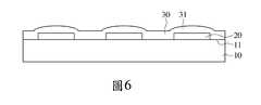
圖1係第一實施例之燈板裝置的側視圖。如圖1所示,第一實施例的燈板裝置1主要應用於背光模組。燈板裝置1包含基板10、複數個發光元件20、膠膜層30、以及遮光油墨層40。發光元件20設置於基板的出光表面11上。膠膜層30覆蓋基板10的出光表面11及發光元件20。膠膜層30包含複數個突起部31,突起部31分別對應於發光元件20。Fig. 1 is a side view of the light board device of the first embodiment. As shown in Fig. 1, the
在此,膠膜層30可以為透明膠膜片,可以避免出光表面11及發光元件20受到空氣中水氣、氧氣的影響,也能不影響發光元件20的出光效果。突起部31是在膠膜片披覆於發光元件20上時,由發光元件20的高度自然產生的突起。Here, the
遮光油墨層40位於膠膜層30上,遮光油墨層40包含複數個遮光圖案41,遮光圖案41分別位於突起部31上。如此,透過減少遮光圖案41與發光元件20之間的距離,可以減少對位公差造成的問題。The light-
在此,發光元件20為點光源,例如,可以為發光二極體(Light Emitting Diode,LED)、迷你發光二極體(Mini LED),或是微型發光二極體(Micro LED)。Here, the
圖2係第一實施例之燈板裝置的俯視圖。由於膠膜層30為透明,在此省略。一般而言,遮光圖案41的面積大於或等於發光元件20的面積。當發光元件20發光時,發出的光線會由遮光圖案41的周圍透出,以此達到將點光源擴散、避免直射的效果,而能有效地改善整個出光的均勻度。Fig. 2 is a top view of the light board device of the first embodiment. Since the
圖2A、圖2B為遮光圖案的俯視圖。同時參照圖2,遮光圖案41可以依據遮光的需求,設計為各種不同的圖案。圖示中的的圖案僅為示例,而非用以限制。實際上也可以採用橢圓、蝶狀、翼狀的態樣。2A and 2B are top views of light shielding patterns. Referring to FIG. 2 at the same time, the light-
圖3係第二實施例之燈板裝置的側視圖。如圖3所示,同時參考圖1,第二實施例的燈板裝置1,除了第一實施例的結構外,更包含第二遮光油墨層50。第二遮光油墨層50包含複數個第二遮光圖案51,且第二遮光圖案51分別位於遮光圖案41上,且各第二遮光圖案51的面積小於各遮光圖案41的面積。由於發光元件20為點光源,其中心位置的亮度較亮,在此實施例設置第二遮光圖案51的目的,是使設計者能依據發光元件20的功率來進行調配。若是發光元件20功率較強時,透過以兩層遮光油墨的方式來處理,來達到所需的出光品質,避免使用單層但過厚而使得遮光油墨,而造成整體光度降低的問題。Fig. 3 is a side view of the light board device of the second embodiment. As shown in FIG. 3 and referring to FIG. 1 at the same time, the
圖4係第三實施例之燈板裝置的側視圖。如圖4所示,第三實施例的結構大致上與第二實施例相同,唯,第二遮光油墨層50與遮光油墨層40為不同顏色。在此,可以達到光線調配之功效,例如,藍光過強時,透過紅光、綠光的第二遮光油墨層50與遮光油墨層40來達到色彩的平衡。然而,以上僅為示例,而非用以限制。Fig. 4 is a side view of the light board device of the third embodiment. As shown in FIG. 4, the structure of the third embodiment is substantially the same as that of the second embodiment, except that the second light-
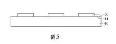
圖5至圖9係第一實施例之燈板裝置製作方法的逐步側視圖。首先,如圖5所示,設置複數個發光元件20於基板10的出光表面11上。接著,如圖6所示,貼附膠膜層30於基板10的出光表面11及發光元件20上。膠膜層30在覆蓋發光元件20處形成複數個突起部31。由於突起部31是由於披覆膠膜層30在發光元件20,基於發光元件20的高度自然形成,因此,突起部31的位置必然與發光元件20相互對應。更詳細地,相互對應係指朝向基板10方向,發光元件20的垂直投影疊設於突起部31的垂直投影。一般來說,突起部31的面積大於等於發光元件20的面積。5 to 9 are step-by-step side views of the manufacturing method of the lamp panel device of the first embodiment. First, as shown in FIG. 5, a plurality of light-emitting
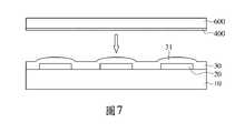
再接著,如圖7所示,同時參照圖1,在轉印治具600設置有油墨400,並對於膠膜層30進行壓印。由於突起部31的高度較高,在其上自然形成油墨圖案45。在完成油墨圖案45後,將突起部31上的油墨圖案45固化,而形成包含複數個遮光圖案41的遮光油墨層40。Then, as shown in FIG. 7 and referring to FIG. 1 at the same time, an
在此,圖8及圖9是一種固化的方式,但這僅為示例,而非用以限制。如圖8所示,在固化的第一階段,是先點亮發光元件20使油墨圖案45進行感光。最後,如圖9所示,最後以照射紫外光的方式,使得遮光油墨層40完全固化。在此,油墨圖案45先進行感光,可以使得油墨圖案45中的高分子產生交聯,如同光阻劑的效果。如此,若是膠膜層30有沾黏到油墨400時,未感光的部分,可以透過清洗的方式加以去除。然而,也可以只採用圖9的方式直接進行固化。Here, FIG. 8 and FIG. 9 are a curing method, but this is only an example, not a limitation. As shown in FIG. 8, in the first stage of curing, the light-emitting
圖10至圖11係第二實施例之燈板裝置製作方法的部分側視圖。如圖10所示,製作第二實施例的燈板裝置時,需先完成第一實施力的製作流程。接著,再次利用設置有第二油墨500的轉印治具600,進行壓印,而在遮光油墨層40上形成第二遮光油墨層50。在此,第二遮光油墨層50除了利用壓印方式形成,亦可以採用噴塗的方式。10 to 11 are partial side views of the manufacturing method of the lamp panel device of the second embodiment. As shown in FIG. 10, when manufacturing the lamp panel device of the second embodiment, the manufacturing process of the first implementation force needs to be completed first. Then, the
接著,參照圖8及圖9的方式,固化第二遮光油墨層50,使得在遮光圖案41上分別形成第二遮光圖案51,且第二遮光圖案51的面積小於遮光圖案41的面積,而完成如圖11的結構。在此,第二遮光圖案51的目的,為調整點光源的出光品質,以避免亮暗不均的狀態。可以如同第二實施例,第二遮光圖案51與遮光圖案41為同色,或是如同第三實施例,第二遮光圖案51與遮光圖案41為不同色。Next, referring to the manner of FIGS. 8 and 9, the second light-shielding
綜上所述,透過膠膜層30隨著出光表面11的起伏自然形成突起部31,再將遮光油墨層40設置於膠膜層30上形成遮光圖案41。透過物理的方式直接減少遮光圖案41與發光元件20之間的對位公差,更進一步減少遮光圖案41與發光元件20之間的距離,而能有效地提升出光品質,提升光源出光的均勻性。In summary, the transparent
雖然本發明的技術內容已經以較佳實施例揭露如上,然其並非用以限定本發明,任何熟習此技藝者,在不脫離本發明之精神所作些許之更動與潤飾,皆應涵蓋於本發明的範疇內,因此本發明之保護範圍當視後附之申請專利範圍所界定者為準。Although the technical content of the present invention has been disclosed in the preferred embodiments as above, it is not intended to limit the present invention. Anyone who is familiar with this technique and makes some changes and modifications without departing from the spirit of the present invention should be covered by the present invention Therefore, the scope of protection of the present invention shall be subject to the scope of the attached patent application.
1:燈板裝置10:基板11:出光表面20:發光元件30:膠膜層31:突起部40:遮光油墨層41:遮光圖案45:油墨圖案50:第二遮光油墨層51:第二遮光圖案400:油墨500:第二油墨600:轉印治具1: Light board device10: substrate11: Light emitting surface20: Light-emitting element30: Film layer31: protrusion40: shading ink layer41: shading pattern45: ink pattern50: The second shading ink layer51: second shading pattern400: ink500: second ink600: transfer fixture
圖1係第一實施例之燈板裝置的側視圖。 圖2係第一實施例之燈板裝置的俯視圖。 圖2A、圖2B為遮光圖案的俯視圖。 圖3係第二實施例之燈板裝置的側視圖。 圖4係第三實施例之燈板裝置的側視圖。 圖5至圖9係第一實施例之燈板裝置製作方法的逐步側視圖。 圖10至圖11係第二實施例之燈板裝置製作方法的部分側視圖。Fig. 1 is a side view of the light board device of the first embodiment. Fig. 2 is a top view of the light board device of the first embodiment. 2A and 2B are top views of light shielding patterns. Fig. 3 is a side view of the light board device of the second embodiment. Fig. 4 is a side view of the light board device of the third embodiment. 5 to 9 are step-by-step side views of the manufacturing method of the lamp panel device of the first embodiment. 10 to 11 are partial side views of the manufacturing method of the lamp panel device of the second embodiment.
1:燈板裝置1: Light board device
10:基板10: substrate
11:出光表面11: Light emitting surface
20:發光元件20: Light-emitting element
30:膠膜層30: Film layer
31:突起部31: protrusion
40:遮光油墨層40: shading ink layer
41:遮光圖案41: shading pattern
Claims (10)
Translated fromChinesePriority Applications (1)
| Application Number | Priority Date | Filing Date | Title |
|---|---|---|---|
| TW109127988ATWI710809B (en) | 2020-08-17 | 2020-08-17 | Light board device and manufacturing method thereof |
Applications Claiming Priority (1)
| Application Number | Priority Date | Filing Date | Title |
|---|---|---|---|
| TW109127988ATWI710809B (en) | 2020-08-17 | 2020-08-17 | Light board device and manufacturing method thereof |
Publications (2)
| Publication Number | Publication Date |
|---|---|
| TWI710809Btrue TWI710809B (en) | 2020-11-21 |
| TW202208901A TW202208901A (en) | 2022-03-01 |
Family
ID=74202517
Family Applications (1)
| Application Number | Title | Priority Date | Filing Date |
|---|---|---|---|
| TW109127988ATWI710809B (en) | 2020-08-17 | 2020-08-17 | Light board device and manufacturing method thereof |
Country Status (1)
| Country | Link |
|---|---|
| TW (1) | TWI710809B (en) |
Cited By (5)
| Publication number | Priority date | Publication date | Assignee | Title |
|---|---|---|---|---|
| TWI777350B (en)* | 2020-12-31 | 2022-09-11 | 友達光電股份有限公司 | Backlight module |
| TWI844001B (en)* | 2022-01-12 | 2024-06-01 | 大陸商友達光電(蘇州)有限公司 | Backlight module |
| TWI848358B (en)* | 2022-08-30 | 2024-07-11 | 林志成 | Backlight module for luminous keyboard |
| TWI849325B (en)* | 2021-07-29 | 2024-07-21 | 大陸商業成光電(深圳)有限公司 | Display module and manufacturing method thereof |
| TWI860543B (en)* | 2022-08-30 | 2024-11-01 | 林志成 | Luminous keyboard luminous module |
Families Citing this family (1)
| Publication number | Priority date | Publication date | Assignee | Title |
|---|---|---|---|---|
| CN115295542A (en)* | 2022-08-18 | 2022-11-04 | 友达光电(苏州)有限公司 | Backlight module and manufacturing method thereof |
Citations (2)
| Publication number | Priority date | Publication date | Assignee | Title |
|---|---|---|---|---|
| US20090261333A1 (en)* | 2008-04-21 | 2009-10-22 | Samsung Electronics Co., Ltd. | Display substrate and method of manufacturing the same |
| CN110888261A (en)* | 2018-12-07 | 2020-03-17 | 鸿富锦精密工业(深圳)有限公司 | Display panel and display device |
- 2020
- 2020-08-17TWTW109127988Apatent/TWI710809B/enactive
Patent Citations (2)
| Publication number | Priority date | Publication date | Assignee | Title |
|---|---|---|---|---|
| US20090261333A1 (en)* | 2008-04-21 | 2009-10-22 | Samsung Electronics Co., Ltd. | Display substrate and method of manufacturing the same |
| CN110888261A (en)* | 2018-12-07 | 2020-03-17 | 鸿富锦精密工业(深圳)有限公司 | Display panel and display device |
Cited By (6)
| Publication number | Priority date | Publication date | Assignee | Title |
|---|---|---|---|---|
| TWI777350B (en)* | 2020-12-31 | 2022-09-11 | 友達光電股份有限公司 | Backlight module |
| US11828976B2 (en) | 2020-12-31 | 2023-11-28 | Au Optronics Corporation | Backlight module and display device using the same |
| TWI849325B (en)* | 2021-07-29 | 2024-07-21 | 大陸商業成光電(深圳)有限公司 | Display module and manufacturing method thereof |
| TWI844001B (en)* | 2022-01-12 | 2024-06-01 | 大陸商友達光電(蘇州)有限公司 | Backlight module |
| TWI848358B (en)* | 2022-08-30 | 2024-07-11 | 林志成 | Backlight module for luminous keyboard |
| TWI860543B (en)* | 2022-08-30 | 2024-11-01 | 林志成 | Luminous keyboard luminous module |
Also Published As
| Publication number | Publication date |
|---|---|
| TW202208901A (en) | 2022-03-01 |
Similar Documents
| Publication | Publication Date | Title |
|---|---|---|
| TWI710809B (en) | Light board device and manufacturing method thereof | |
| US20120218752A1 (en) | Light source module and optical member | |
| US20210373365A1 (en) | Light-curing 3D printer optical machine, printer and method of luminous display | |
| WO2021228282A1 (en) | Light source module and atmosphere lamp glass used for atmosphere lamp | |
| KR20210047204A (en) | Direct type back light device and display apparatus having the same | |
| TW202014775A (en) | Light source module and display appartus | |
| TWI736046B (en) | Backlight unit and display device including the same | |
| CN112230475A (en) | Edge light-emitting uniform high-color gamut direct type backlight module | |
| CN114141913A (en) | Manufacturing method of backlight panel, backlight panel and backlight module | |
| WO2022089337A1 (en) | Light-transmissive ornament | |
| WO2019071700A1 (en) | Liquid crystal display and backlight module thereof | |
| WO2006064593A1 (en) | Lighting equipment and lighting system | |
| WO2020207102A1 (en) | Area light source device and manufacturing method therefor, display device | |
| CN103791274B (en) | Planar light source generating device | |
| TW202020364A (en) | Illuminating mechanism, backlight module, and display device | |
| CN219123134U (en) | Keyboard structure of color backlight module | |
| KR101211715B1 (en) | Backlight unit and Fabricating method of the same | |
| KR102155320B1 (en) | Lighting apparatus based on fluorescent printed type PCB substrate | |
| KR100528894B1 (en) | Organic electroluminescene display and method thereof | |
| JP4463074B2 (en) | LIGHTING DEVICE AND METHOD FOR FORMING LAYER ON GLASS PLATE USED FOR LIGHTING DEVICE | |
| CN205485182U (en) | Straight following formula LCD module backlight subassembly | |
| KR101446917B1 (en) | Lamp device and Fabricating method of the same | |
| CN222319251U (en) | A multi-color light guide component structure | |
| CN220753466U (en) | Promote light-emitting even sex miniLED Structure of the | |
| CN221805004U (en) | Display screen and light-emitting device thereof |