TWI709952B - Electronic device and driving method of electronic device - Google Patents
Electronic device and driving method of electronic deviceDownload PDFInfo
- Publication number
- TWI709952B TWI709952BTW105137469ATW105137469ATWI709952BTW I709952 BTWI709952 BTW I709952BTW 105137469 ATW105137469 ATW 105137469ATW 105137469 ATW105137469 ATW 105137469ATW I709952 BTWI709952 BTW I709952B
- Authority
- TW
- Taiwan
- Prior art keywords
- display
- light
- layer
- display element
- electronic device
- Prior art date
Links
- 238000000034methodMethods0.000titleclaimsdescription63
- 238000001514detection methodMethods0.000claimsabstractdescription38
- 238000003384imaging methodMethods0.000claimsabstractdescription31
- 239000004973liquid crystal related substanceSubstances0.000claimsdescription125
- 239000000126substanceSubstances0.000claimsdescription19
- 239000010410layerSubstances0.000description744
- 229920005989resinPolymers0.000description162
- 239000011347resinSubstances0.000description162
- 239000010408filmSubstances0.000description122
- 239000000758substrateSubstances0.000description94
- 239000004065semiconductorSubstances0.000description90
- 239000000463materialSubstances0.000description86
- 238000009413insulationMethods0.000description40
- 239000012790adhesive layerSubstances0.000description37
- 230000006870functionEffects0.000description37
- 239000011701zincSubstances0.000description31
- 238000010586diagramMethods0.000description25
- PXHVJJICTQNCMI-UHFFFAOYSA-NNickelChemical compound[Ni]PXHVJJICTQNCMI-UHFFFAOYSA-N0.000description24
- XAGFODPZIPBFFR-UHFFFAOYSA-NaluminiumChemical compound[Al]XAGFODPZIPBFFR-UHFFFAOYSA-N0.000description22
- 229910052751metalInorganic materials0.000description22
- XLOMVQKBTHCTTD-UHFFFAOYSA-NZinc monoxideChemical compound[Zn]=OXLOMVQKBTHCTTD-UHFFFAOYSA-N0.000description20
- 239000002184metalSubstances0.000description19
- 239000007769metal materialSubstances0.000description19
- 229910052782aluminiumInorganic materials0.000description18
- RYGMFSIKBFXOCR-UHFFFAOYSA-NCopperChemical compound[Cu]RYGMFSIKBFXOCR-UHFFFAOYSA-N0.000description17
- 239000000956alloySubstances0.000description17
- 239000010949copperSubstances0.000description17
- 229910052802copperInorganic materials0.000description16
- 229910045601alloyInorganic materials0.000description15
- 230000003287optical effectEffects0.000description15
- XUIMIQQOPSSXEZ-UHFFFAOYSA-NSiliconChemical compound[Si]XUIMIQQOPSSXEZ-UHFFFAOYSA-N0.000description14
- 229910052710siliconInorganic materials0.000description14
- 239000010703siliconSubstances0.000description14
- RTAQQCXQSZGOHL-UHFFFAOYSA-NTitaniumChemical compound[Ti]RTAQQCXQSZGOHL-UHFFFAOYSA-N0.000description13
- 229910052719titaniumInorganic materials0.000description13
- 239000010936titaniumSubstances0.000description13
- XLYOFNOQVPJJNP-UHFFFAOYSA-NwaterSubstancesOXLYOFNOQVPJJNP-UHFFFAOYSA-N0.000description13
- XEEYBQQBJWHFJM-UHFFFAOYSA-NIronChemical compound[Fe]XEEYBQQBJWHFJM-UHFFFAOYSA-N0.000description12
- KDLHZDBZIXYQEI-UHFFFAOYSA-NPalladiumChemical compound[Pd]KDLHZDBZIXYQEI-UHFFFAOYSA-N0.000description12
- IJGRMHOSHXDMSA-UHFFFAOYSA-NAtomic nitrogenChemical compoundN#NIJGRMHOSHXDMSA-UHFFFAOYSA-N0.000description11
- 230000001747exhibiting effectEffects0.000description11
- 239000011521glassSubstances0.000description11
- 229910052759nickelInorganic materials0.000description11
- 239000002096quantum dotSubstances0.000description11
- FYYHWMGAXLPEAU-UHFFFAOYSA-NMagnesiumChemical compound[Mg]FYYHWMGAXLPEAU-UHFFFAOYSA-N0.000description10
- 239000012535impuritySubstances0.000description10
- AMGQUBHHOARCQH-UHFFFAOYSA-Nindium;oxotinChemical compound[In].[Sn]=OAMGQUBHHOARCQH-UHFFFAOYSA-N0.000description10
- 239000011777magnesiumSubstances0.000description10
- 230000008569processEffects0.000description10
- 239000004332silverSubstances0.000description10
- 239000011787zinc oxideSubstances0.000description10
- 229910000838Al alloyInorganic materials0.000description9
- ZOKXTWBITQBERF-UHFFFAOYSA-NMolybdenumChemical compound[Mo]ZOKXTWBITQBERF-UHFFFAOYSA-N0.000description9
- 239000000835fiberSubstances0.000description9
- 239000011159matrix materialSubstances0.000description9
- 239000000203mixtureSubstances0.000description9
- 229910052750molybdenumInorganic materials0.000description9
- 239000011733molybdenumSubstances0.000description9
- -1polyethylene terephthalatePolymers0.000description9
- 229910052709silverInorganic materials0.000description9
- 239000010937tungstenSubstances0.000description9
- WFKWXMTUELFFGS-UHFFFAOYSA-NtungstenChemical compound[W]WFKWXMTUELFFGS-UHFFFAOYSA-N0.000description9
- 229910052721tungstenInorganic materials0.000description9
- VYPSYNLAJGMNEJ-UHFFFAOYSA-NSilicium dioxideChemical compoundO=[Si]=OVYPSYNLAJGMNEJ-UHFFFAOYSA-N0.000description8
- 239000003086colorantSubstances0.000description8
- 150000001875compoundsChemical class0.000description8
- 230000005684electric fieldEffects0.000description8
- 229910052733galliumInorganic materials0.000description8
- 229910052738indiumInorganic materials0.000description8
- 229910052760oxygenInorganic materials0.000description8
- BASFCYQUMIYNBI-UHFFFAOYSA-NplatinumChemical compound[Pt]BASFCYQUMIYNBI-UHFFFAOYSA-N0.000description8
- 229920001721polyimidePolymers0.000description8
- 125000006850spacer groupChemical group0.000description8
- 239000000853adhesiveSubstances0.000description7
- 230000001070adhesive effectEffects0.000description7
- 239000003990capacitorSubstances0.000description7
- 230000000694effectsEffects0.000description7
- 229910003437indium oxideInorganic materials0.000description7
- PJXISJQVUVHSOJ-UHFFFAOYSA-Nindium(iii) oxideChemical compound[O-2].[O-2].[O-2].[In+3].[In+3]PJXISJQVUVHSOJ-UHFFFAOYSA-N0.000description7
- 229910044991metal oxideInorganic materials0.000description7
- 150000004706metal oxidesChemical class0.000description7
- 238000011282treatmentMethods0.000description7
- 229910001316Ag alloyInorganic materials0.000description6
- GYHNNYVSQQEPJS-UHFFFAOYSA-NGalliumChemical compound[Ga]GYHNNYVSQQEPJS-UHFFFAOYSA-N0.000description6
- 229910052779NeodymiumInorganic materials0.000description6
- 229910052581Si3N4Inorganic materials0.000description6
- QVGXLLKOCUKJST-UHFFFAOYSA-Natomic oxygenChemical compound[O]QVGXLLKOCUKJST-UHFFFAOYSA-N0.000description6
- 239000004020conductorSubstances0.000description6
- 239000013078crystalSubstances0.000description6
- 238000000605extractionMethods0.000description6
- PCHJSUWPFVWCPO-UHFFFAOYSA-NgoldChemical compound[Au]PCHJSUWPFVWCPO-UHFFFAOYSA-N0.000description6
- 229910052737goldInorganic materials0.000description6
- 239000010931goldSubstances0.000description6
- APFVFJFRJDLVQX-UHFFFAOYSA-Nindium atomChemical compound[In]APFVFJFRJDLVQX-UHFFFAOYSA-N0.000description6
- 229910052742ironInorganic materials0.000description6
- 229910052749magnesiumInorganic materials0.000description6
- 238000004519manufacturing processMethods0.000description6
- 238000002156mixingMethods0.000description6
- QEFYFXOXNSNQGX-UHFFFAOYSA-Nneodymium atomChemical compound[Nd]QEFYFXOXNSNQGX-UHFFFAOYSA-N0.000description6
- 239000001301oxygenSubstances0.000description6
- 230000035699permeabilityEffects0.000description6
- HQVNEWCFYHHQES-UHFFFAOYSA-Nsilicon nitrideChemical compoundN12[Si]34N5[Si]62N3[Si]51N64HQVNEWCFYHHQES-UHFFFAOYSA-N0.000description6
- OKTJSMMVPCPJKN-UHFFFAOYSA-NCarbonChemical compound[C]OKTJSMMVPCPJKN-UHFFFAOYSA-N0.000description5
- VYZAMTAEIAYCRO-UHFFFAOYSA-NChromiumChemical compound[Cr]VYZAMTAEIAYCRO-UHFFFAOYSA-N0.000description5
- UFHFLCQGNIYNRP-UHFFFAOYSA-NHydrogenChemical compound[H][H]UFHFLCQGNIYNRP-UHFFFAOYSA-N0.000description5
- BQCADISMDOOEFD-UHFFFAOYSA-NSilverChemical compound[Ag]BQCADISMDOOEFD-UHFFFAOYSA-N0.000description5
- GWEVSGVZZGPLCZ-UHFFFAOYSA-NTitan oxideChemical compoundO=[Ti]=OGWEVSGVZZGPLCZ-UHFFFAOYSA-N0.000description5
- QCWXUUIWCKQGHC-UHFFFAOYSA-NZirconiumChemical compound[Zr]QCWXUUIWCKQGHC-UHFFFAOYSA-N0.000description5
- 230000005540biological transmissionEffects0.000description5
- 239000011651chromiumSubstances0.000description5
- 229910052804chromiumInorganic materials0.000description5
- 239000007789gasSubstances0.000description5
- 229910052732germaniumInorganic materials0.000description5
- GNPVGFCGXDBREM-UHFFFAOYSA-Ngermanium atomChemical compound[Ge]GNPVGFCGXDBREM-UHFFFAOYSA-N0.000description5
- 229910021389grapheneInorganic materials0.000description5
- 239000001257hydrogenSubstances0.000description5
- 229910052739hydrogenInorganic materials0.000description5
- 229910052746lanthanumInorganic materials0.000description5
- FZLIPJUXYLNCLC-UHFFFAOYSA-Nlanthanum atomChemical compound[La]FZLIPJUXYLNCLC-UHFFFAOYSA-N0.000description5
- 150000002739metalsChemical class0.000description5
- 229910052757nitrogenInorganic materials0.000description5
- 229910052763palladiumInorganic materials0.000description5
- 239000002245particleSubstances0.000description5
- 238000012545processingMethods0.000description5
- 238000004544sputter depositionMethods0.000description5
- 239000010409thin filmSubstances0.000description5
- OGIDPMRJRNCKJF-UHFFFAOYSA-Ntitanium oxideInorganic materials[Ti]=OOGIDPMRJRNCKJF-UHFFFAOYSA-N0.000description5
- 229910052725zincInorganic materials0.000description5
- YVTHLONGBIQYBO-UHFFFAOYSA-Nzinc indium(3+) oxygen(2-)Chemical compound[O--].[Zn++].[In+3]YVTHLONGBIQYBO-UHFFFAOYSA-N0.000description5
- 229910052726zirconiumInorganic materials0.000description5
- MYMOFIZGZYHOMD-UHFFFAOYSA-NDioxygenChemical compoundO=OMYMOFIZGZYHOMD-UHFFFAOYSA-N0.000description4
- 229910000861Mg alloyInorganic materials0.000description4
- 239000004642PolyimideSubstances0.000description4
- QVQLCTNNEUAWMS-UHFFFAOYSA-Nbarium oxideChemical compound[Ba]=OQVQLCTNNEUAWMS-UHFFFAOYSA-N0.000description4
- 230000015572biosynthetic processEffects0.000description4
- 239000010941cobaltSubstances0.000description4
- 229910017052cobaltInorganic materials0.000description4
- GUTLYIVDDKVIGB-UHFFFAOYSA-Ncobalt atomChemical compound[Co]GUTLYIVDDKVIGB-UHFFFAOYSA-N0.000description4
- 230000000295complement effectEffects0.000description4
- 239000002131composite materialSubstances0.000description4
- 229910001882dioxygenInorganic materials0.000description4
- 238000002149energy-dispersive X-ray emission spectroscopyMethods0.000description4
- 239000000284extractSubstances0.000description4
- 230000005669field effectEffects0.000description4
- 239000003365glass fiberSubstances0.000description4
- 238000010438heat treatmentMethods0.000description4
- 229910010272inorganic materialInorganic materials0.000description4
- 230000031700light absorptionEffects0.000description4
- TWNQGVIAIRXVLR-UHFFFAOYSA-Noxo(oxoalumanyloxy)alumaneChemical compoundO=[Al]O[Al]=OTWNQGVIAIRXVLR-UHFFFAOYSA-N0.000description4
- 229910052697platinumInorganic materials0.000description4
- 239000009719polyimide resinSubstances0.000description4
- 229910052814silicon oxideInorganic materials0.000description4
- 229910052727yttriumInorganic materials0.000description4
- VWQVUPCCIRVNHF-UHFFFAOYSA-Nyttrium atomChemical compound[Y]VWQVUPCCIRVNHF-UHFFFAOYSA-N0.000description4
- UWCWUCKPEYNDNV-LBPRGKRZSA-N2,6-dimethyl-n-[[(2s)-pyrrolidin-2-yl]methyl]anilineChemical compoundCC1=CC=CC(C)=C1NC[C@H]1NCCC1UWCWUCKPEYNDNV-LBPRGKRZSA-N0.000description3
- 241001270131Agaricus moelleriSpecies0.000description3
- 229910052684CeriumInorganic materials0.000description3
- 239000004983Polymer Dispersed Liquid CrystalSubstances0.000description3
- NRTOMJZYCJJWKI-UHFFFAOYSA-NTitanium nitrideChemical compound[Ti]#NNRTOMJZYCJJWKI-UHFFFAOYSA-N0.000description3
- 238000002441X-ray diffractionMethods0.000description3
- HCHKCACWOHOZIP-UHFFFAOYSA-NZincChemical compound[Zn]HCHKCACWOHOZIP-UHFFFAOYSA-N0.000description3
- ZMIGMASIKSOYAM-UHFFFAOYSA-NceriumChemical compound[Ce][Ce][Ce][Ce][Ce][Ce][Ce][Ce][Ce][Ce][Ce][Ce][Ce][Ce][Ce][Ce][Ce][Ce][Ce][Ce][Ce][Ce][Ce][Ce][Ce][Ce][Ce][Ce][Ce][Ce][Ce][Ce][Ce][Ce][Ce][Ce][Ce][Ce]ZMIGMASIKSOYAM-UHFFFAOYSA-N0.000description3
- 238000006243chemical reactionMethods0.000description3
- PMHQVHHXPFUNSP-UHFFFAOYSA-Mcopper(1+);methylsulfanylmethane;bromideChemical compoundBr[Cu].CSCPMHQVHHXPFUNSP-UHFFFAOYSA-M0.000description3
- 238000000151depositionMethods0.000description3
- 230000008021depositionEffects0.000description3
- 230000006866deteriorationEffects0.000description3
- 239000003822epoxy resinSubstances0.000description3
- 239000005262ferroelectric liquid crystals (FLCs)Substances0.000description3
- 229910052735hafniumInorganic materials0.000description3
- VBJZVLUMGGDVMO-UHFFFAOYSA-Nhafnium atomChemical compound[Hf]VBJZVLUMGGDVMO-UHFFFAOYSA-N0.000description3
- 150000002484inorganic compoundsChemical class0.000description3
- 239000011810insulating materialSubstances0.000description3
- 230000001678irradiating effectEffects0.000description3
- 238000010030laminatingMethods0.000description3
- 150000004767nitridesChemical class0.000description3
- 230000003071parasitic effectEffects0.000description3
- 229910021420polycrystalline siliconInorganic materials0.000description3
- 229920000647polyepoxidePolymers0.000description3
- 229920000139polyethylene terephthalatePolymers0.000description3
- 239000005020polyethylene terephthalateSubstances0.000description3
- 229920000915polyvinyl chloridePolymers0.000description3
- 239000004800polyvinyl chlorideSubstances0.000description3
- 238000007639printingMethods0.000description3
- 239000002356single layerSubstances0.000description3
- 238000005477sputtering targetMethods0.000description3
- 229910052715tantalumInorganic materials0.000description3
- GUVRBAGPIYLISA-UHFFFAOYSA-Ntantalum atomChemical compound[Ta]GUVRBAGPIYLISA-UHFFFAOYSA-N0.000description3
- 229920001187thermosetting polymerPolymers0.000description3
- 238000007740vapor depositionMethods0.000description3
- 229920000178Acrylic resinPolymers0.000description2
- 239000004925Acrylic resinSubstances0.000description2
- XKRFYHLGVUSROY-UHFFFAOYSA-NArgonChemical compound[Ar]XKRFYHLGVUSROY-UHFFFAOYSA-N0.000description2
- ZOXJGFHDIHLPTG-UHFFFAOYSA-NBoronChemical compound[B]ZOXJGFHDIHLPTG-UHFFFAOYSA-N0.000description2
- 229910000881Cu alloyInorganic materials0.000description2
- 229910000990Ni alloyInorganic materials0.000description2
- ATJFFYVFTNAWJD-UHFFFAOYSA-NTinChemical compound[Sn]ATJFFYVFTNAWJD-UHFFFAOYSA-N0.000description2
- 229910021536ZeoliteInorganic materials0.000description2
- 239000012298atmosphereSubstances0.000description2
- GPBUGPUPKAGMDK-UHFFFAOYSA-NazanylidynemolybdenumChemical compound[Mo]#NGPBUGPUPKAGMDK-UHFFFAOYSA-N0.000description2
- 238000005452bendingMethods0.000description2
- 229910052790berylliumInorganic materials0.000description2
- ATBAMAFKBVZNFJ-UHFFFAOYSA-Nberyllium atomChemical compound[Be]ATBAMAFKBVZNFJ-UHFFFAOYSA-N0.000description2
- 229910052796boronInorganic materials0.000description2
- HVYWMOMLDIMFJA-DPAQBDIFSA-NcholesterolChemical compoundC1C=C2C[C@@H](O)CC[C@]2(C)[C@@H]2[C@@H]1[C@@H]1CC[C@H]([C@H](C)CCCC(C)C)[C@@]1(C)CC2HVYWMOMLDIMFJA-DPAQBDIFSA-N0.000description2
- 238000000576coating methodMethods0.000description2
- 239000011258core-shell materialSubstances0.000description2
- 239000002274desiccantSubstances0.000description2
- 238000009792diffusion processMethods0.000description2
- HNPSIPDUKPIQMN-UHFFFAOYSA-Ndioxosilane;oxo(oxoalumanyloxy)alumaneChemical compoundO=[Si]=O.O=[Al]O[Al]=OHNPSIPDUKPIQMN-UHFFFAOYSA-N0.000description2
- 238000005401electroluminescenceMethods0.000description2
- 238000002524electron diffraction dataMethods0.000description2
- 238000001962electrophoresisMethods0.000description2
- 238000007687exposure techniqueMethods0.000description2
- 239000012530fluidSubstances0.000description2
- 230000004313glareEffects0.000description2
- 230000012447hatchingEffects0.000description2
- 210000003128headAnatomy0.000description2
- 230000005525hole transportEffects0.000description2
- 238000005499laser crystallizationMethods0.000description2
- 238000004020luminiscence typeMethods0.000description2
- 238000013507mappingMethods0.000description2
- 238000005259measurementMethods0.000description2
- 239000003094microcapsuleSubstances0.000description2
- 238000012986modificationMethods0.000description2
- 230000004048modificationEffects0.000description2
- 239000002159nanocrystalSubstances0.000description2
- QGLKJKCYBOYXKC-UHFFFAOYSA-NnonaoxidotritungstenChemical compoundO=[W]1(=O)O[W](=O)(=O)O[W](=O)(=O)O1QGLKJKCYBOYXKC-UHFFFAOYSA-N0.000description2
- 239000011368organic materialSubstances0.000description2
- 230000003647oxidationEffects0.000description2
- 238000007254oxidation reactionMethods0.000description2
- 229920002037poly(vinyl butyral) polymerPolymers0.000description2
- 229920006122polyamide resinPolymers0.000description2
- 229920005591polysiliconPolymers0.000description2
- 239000004810polytetrafluoroethyleneSubstances0.000description2
- 229920001343polytetrafluoroethylenePolymers0.000description2
- 239000000843powderSubstances0.000description2
- 238000007789sealingMethods0.000description2
- 235000012239silicon dioxideNutrition0.000description2
- 229920002050silicone resinPolymers0.000description2
- 238000001179sorption measurementMethods0.000description2
- 230000003595spectral effectEffects0.000description2
- 229910052718tinInorganic materials0.000description2
- 229910001930tungsten oxideInorganic materials0.000description2
- 229910052720vanadiumInorganic materials0.000description2
- GPPXJZIENCGNKB-UHFFFAOYSA-NvanadiumChemical compound[V]#[V]GPPXJZIENCGNKB-UHFFFAOYSA-N0.000description2
- 239000010457zeoliteSubstances0.000description2
- 229920000049Carbon (fiber)Polymers0.000description1
- 239000004986Cholesteric liquid crystals (ChLC)Substances0.000description1
- 239000005264High molar mass liquid crystalSubstances0.000description1
- 206010021143HypoxiaDiseases0.000description1
- 229910000858La alloyInorganic materials0.000description1
- 229910000583Nd alloyInorganic materials0.000description1
- 229910001252Pd alloyInorganic materials0.000description1
- 229910002668Pd-CuInorganic materials0.000description1
- OAICVXFJPJFONN-UHFFFAOYSA-NPhosphorusChemical compound[P]OAICVXFJPJFONN-UHFFFAOYSA-N0.000description1
- 239000004952PolyamideSubstances0.000description1
- 239000004962Polyamide-imideSubstances0.000description1
- 239000004698PolyethyleneSubstances0.000description1
- 239000004721Polyphenylene oxideSubstances0.000description1
- 239000004372Polyvinyl alcoholSubstances0.000description1
- BUGBHKTXTAQXES-UHFFFAOYSA-NSeleniumChemical compound[Se]BUGBHKTXTAQXES-UHFFFAOYSA-N0.000description1
- 239000004990Smectic liquid crystalSubstances0.000description1
- NINIDFKCEFEMDL-UHFFFAOYSA-NSulfurChemical compound[S]NINIDFKCEFEMDL-UHFFFAOYSA-N0.000description1
- UCKMPCXJQFINFW-UHFFFAOYSA-NSulphideChemical compound[S-2]UCKMPCXJQFINFW-UHFFFAOYSA-N0.000description1
- 239000004974Thermotropic liquid crystalSubstances0.000description1
- 229910001069Ti alloyInorganic materials0.000description1
- 229910009367Zn MInorganic materials0.000description1
- 229910000287alkaline earth metal oxideInorganic materials0.000description1
- PNEYBMLMFCGWSK-UHFFFAOYSA-Naluminium oxideInorganic materials[O-2].[O-2].[O-2].[Al+3].[Al+3]PNEYBMLMFCGWSK-UHFFFAOYSA-N0.000description1
- 150000001408amidesChemical class0.000description1
- 239000004760aramidSubstances0.000description1
- 229910052786argonInorganic materials0.000description1
- 238000000149argon plasma sinteringMethods0.000description1
- 229920003235aromatic polyamidePolymers0.000description1
- 229910052785arsenicInorganic materials0.000description1
- RQNWIZPPADIBDY-UHFFFAOYSA-Narsenic atomChemical compound[As]RQNWIZPPADIBDY-UHFFFAOYSA-N0.000description1
- 125000003118aryl groupChemical group0.000description1
- 208000003464asthenopiaDiseases0.000description1
- 230000004888barrier functionEffects0.000description1
- 230000008901benefitEffects0.000description1
- 230000000903blocking effectEffects0.000description1
- DQXBYHZEEUGOBF-UHFFFAOYSA-Nbut-3-enoic acid;etheneChemical compoundC=C.OC(=O)CC=CDQXBYHZEEUGOBF-UHFFFAOYSA-N0.000description1
- 229910052793cadmiumInorganic materials0.000description1
- BDOSMKKIYDKNTQ-UHFFFAOYSA-Ncadmium atomChemical compound[Cd]BDOSMKKIYDKNTQ-UHFFFAOYSA-N0.000description1
- BRPQOXSCLDDYGP-UHFFFAOYSA-Ncalcium oxideChemical compound[O-2].[Ca+2]BRPQOXSCLDDYGP-UHFFFAOYSA-N0.000description1
- ODINCKMPIJJUCX-UHFFFAOYSA-Ncalcium oxideInorganic materials[Ca]=OODINCKMPIJJUCX-UHFFFAOYSA-N0.000description1
- 239000000292calcium oxideSubstances0.000description1
- 239000006229carbon blackSubstances0.000description1
- 239000004917carbon fiberSubstances0.000description1
- 239000000969carrierSubstances0.000description1
- 239000000919ceramicSubstances0.000description1
- 230000003098cholesteric effectEffects0.000description1
- 235000012000cholesterolNutrition0.000description1
- 238000004040coloringMethods0.000description1
- 230000006835compressionEffects0.000description1
- 238000007906compressionMethods0.000description1
- 238000002425crystallisationMethods0.000description1
- 230000008025crystallizationEffects0.000description1
- 150000001925cycloalkenesChemical class0.000description1
- 230000007547defectEffects0.000description1
- 239000000412dendrimerSubstances0.000description1
- 229920000736dendritic polymerPolymers0.000description1
- 238000013461designMethods0.000description1
- 238000011161developmentMethods0.000description1
- 230000018109developmental processEffects0.000description1
- AJNVQOSZGJRYEI-UHFFFAOYSA-Ndigallium;oxygen(2-)Chemical compound[O-2].[O-2].[O-2].[Ga+3].[Ga+3]AJNVQOSZGJRYEI-UHFFFAOYSA-N0.000description1
- 229910001873dinitrogenInorganic materials0.000description1
- 238000007598dipping methodMethods0.000description1
- 239000000975dyeSubstances0.000description1
- 230000005489elastic deformationEffects0.000description1
- 238000004070electrodepositionMethods0.000description1
- 238000010894electron beam technologyMethods0.000description1
- 238000000295emission spectrumMethods0.000description1
- 238000005530etchingMethods0.000description1
- 239000005038ethylene vinyl acetateSubstances0.000description1
- 238000001704evaporationMethods0.000description1
- 239000000945fillerSubstances0.000description1
- 238000010304firingMethods0.000description1
- 229910001195gallium oxideInorganic materials0.000description1
- LNEPOXFFQSENCJ-UHFFFAOYSA-NhaloperidolChemical compoundC1CC(O)(C=2C=CC(Cl)=CC=2)CCN1CCCC(=O)C1=CC=C(F)C=C1LNEPOXFFQSENCJ-UHFFFAOYSA-N0.000description1
- 239000011261inert gasSubstances0.000description1
- 238000002347injectionMethods0.000description1
- 239000007924injectionSubstances0.000description1
- 239000011256inorganic fillerSubstances0.000description1
- 229910003475inorganic fillerInorganic materials0.000description1
- 239000011147inorganic materialSubstances0.000description1
- WPBNNNQJVZRUHP-UHFFFAOYSA-Lmanganese(2+);methyl n-[[2-(methoxycarbonylcarbamothioylamino)phenyl]carbamothioyl]carbamate;n-[2-(sulfidocarbothioylamino)ethyl]carbamodithioateChemical compound[Mn+2].[S-]C(=S)NCCNC([S-])=S.COC(=O)NC(=S)NC1=CC=CC=C1NC(=S)NC(=O)OCWPBNNNQJVZRUHP-UHFFFAOYSA-L0.000description1
- 238000000691measurement methodMethods0.000description1
- 230000007246mechanismEffects0.000description1
- 239000012528membraneSubstances0.000description1
- VNWKTOKETHGBQD-UHFFFAOYSA-NmethaneChemical compoundCVNWKTOKETHGBQD-UHFFFAOYSA-N0.000description1
- 150000002894organic compoundsChemical class0.000description1
- 230000001590oxidative effectEffects0.000description1
- 239000005011phenolic resinSubstances0.000description1
- 229910052698phosphorusInorganic materials0.000description1
- 239000011574phosphorusSubstances0.000description1
- 229920002120photoresistant polymerPolymers0.000description1
- 239000000049pigmentSubstances0.000description1
- 238000009832plasma treatmentMethods0.000description1
- 229920003023plasticPolymers0.000description1
- 239000004033plasticSubstances0.000description1
- 238000007747platingMethods0.000description1
- 229920003207poly(ethylene-2,6-naphthalate)Polymers0.000description1
- 229920001200poly(ethylene-vinyl acetate)Polymers0.000description1
- 229920003229poly(methyl methacrylate)Polymers0.000description1
- 229920006350polyacrylonitrile resinPolymers0.000description1
- 229920002647polyamidePolymers0.000description1
- 229920002312polyamide-imidePolymers0.000description1
- 239000004417polycarbonateSubstances0.000description1
- 229920000515polycarbonatePolymers0.000description1
- 229920000728polyesterPolymers0.000description1
- 229920001225polyester resinPolymers0.000description1
- 239000004645polyester resinSubstances0.000description1
- 229920000570polyetherPolymers0.000description1
- 229920000573polyethylenePolymers0.000description1
- 239000011112polyethylene naphthalateSubstances0.000description1
- 229920000642polymerPolymers0.000description1
- 239000004926polymethyl methacrylateSubstances0.000description1
- 229920005990polystyrene resinPolymers0.000description1
- 229920002451polyvinyl alcoholPolymers0.000description1
- 238000010248power generationMethods0.000description1
- 238000003825pressingMethods0.000description1
- 239000010453quartzSubstances0.000description1
- 230000009467reductionEffects0.000description1
- 238000009877renderingMethods0.000description1
- 230000004044responseEffects0.000description1
- 239000010980sapphireSubstances0.000description1
- 229910052594sapphireInorganic materials0.000description1
- 238000007650screen-printingMethods0.000description1
- 229910052711seleniumInorganic materials0.000description1
- 239000011669seleniumSubstances0.000description1
- 229910002027silica gelInorganic materials0.000description1
- 239000000741silica gelSubstances0.000description1
- 239000000377silicon dioxideSubstances0.000description1
- 239000006104solid solutionSubstances0.000description1
- 238000001228spectrumMethods0.000description1
- 238000004528spin coatingMethods0.000description1
- 239000010935stainless steelSubstances0.000description1
- 229910001220stainless steelInorganic materials0.000description1
- 230000003068static effectEffects0.000description1
- 238000003860storageMethods0.000description1
- 229910052717sulfurInorganic materials0.000description1
- 239000011593sulfurSubstances0.000description1
- 238000005211surface analysisMethods0.000description1
- JBQYATWDVHIOAR-UHFFFAOYSA-NtellanylidenegermaniumChemical compound[Te]=[Ge]JBQYATWDVHIOAR-UHFFFAOYSA-N0.000description1
- 229910052714telluriumInorganic materials0.000description1
- PORWMNRCUJJQNO-UHFFFAOYSA-Ntellurium atomChemical compound[Te]PORWMNRCUJJQNO-UHFFFAOYSA-N0.000description1
- 238000012360testing methodMethods0.000description1
- XOLBLPGZBRYERU-UHFFFAOYSA-Ntin dioxideChemical compoundO=[Sn]=OXOLBLPGZBRYERU-UHFFFAOYSA-N0.000description1
- 229910001887tin oxideInorganic materials0.000description1
- 238000012546transferMethods0.000description1
- 238000002834transmittanceMethods0.000description1
Images


Classifications
- G—PHYSICS
- G09—EDUCATION; CRYPTOGRAPHY; DISPLAY; ADVERTISING; SEALS
- G09G—ARRANGEMENTS OR CIRCUITS FOR CONTROL OF INDICATING DEVICES USING STATIC MEANS TO PRESENT VARIABLE INFORMATION
- G09G3/00—Control arrangements or circuits, of interest only in connection with visual indicators other than cathode-ray tubes
- G09G3/20—Control arrangements or circuits, of interest only in connection with visual indicators other than cathode-ray tubes for presentation of an assembly of a number of characters, e.g. a page, by composing the assembly by combination of individual elements arranged in a matrix no fixed position being assigned to or needed to be assigned to the individual characters or partial characters
- G09G3/2092—Details of a display terminals using a flat panel, the details relating to the control arrangement of the display terminal and to the interfaces thereto
- G—PHYSICS
- G09—EDUCATION; CRYPTOGRAPHY; DISPLAY; ADVERTISING; SEALS
- G09G—ARRANGEMENTS OR CIRCUITS FOR CONTROL OF INDICATING DEVICES USING STATIC MEANS TO PRESENT VARIABLE INFORMATION
- G09G3/00—Control arrangements or circuits, of interest only in connection with visual indicators other than cathode-ray tubes
- G09G3/20—Control arrangements or circuits, of interest only in connection with visual indicators other than cathode-ray tubes for presentation of an assembly of a number of characters, e.g. a page, by composing the assembly by combination of individual elements arranged in a matrix no fixed position being assigned to or needed to be assigned to the individual characters or partial characters
- G09G3/22—Control arrangements or circuits, of interest only in connection with visual indicators other than cathode-ray tubes for presentation of an assembly of a number of characters, e.g. a page, by composing the assembly by combination of individual elements arranged in a matrix no fixed position being assigned to or needed to be assigned to the individual characters or partial characters using controlled light sources
- G09G3/30—Control arrangements or circuits, of interest only in connection with visual indicators other than cathode-ray tubes for presentation of an assembly of a number of characters, e.g. a page, by composing the assembly by combination of individual elements arranged in a matrix no fixed position being assigned to or needed to be assigned to the individual characters or partial characters using controlled light sources using electroluminescent panels
- G09G3/32—Control arrangements or circuits, of interest only in connection with visual indicators other than cathode-ray tubes for presentation of an assembly of a number of characters, e.g. a page, by composing the assembly by combination of individual elements arranged in a matrix no fixed position being assigned to or needed to be assigned to the individual characters or partial characters using controlled light sources using electroluminescent panels semiconductive, e.g. using light-emitting diodes [LED]
- G—PHYSICS
- G02—OPTICS
- G02F—OPTICAL DEVICES OR ARRANGEMENTS FOR THE CONTROL OF LIGHT BY MODIFICATION OF THE OPTICAL PROPERTIES OF THE MEDIA OF THE ELEMENTS INVOLVED THEREIN; NON-LINEAR OPTICS; FREQUENCY-CHANGING OF LIGHT; OPTICAL LOGIC ELEMENTS; OPTICAL ANALOGUE/DIGITAL CONVERTERS
- G02F1/00—Devices or arrangements for the control of the intensity, colour, phase, polarisation or direction of light arriving from an independent light source, e.g. switching, gating or modulating; Non-linear optics
- G02F1/01—Devices or arrangements for the control of the intensity, colour, phase, polarisation or direction of light arriving from an independent light source, e.g. switching, gating or modulating; Non-linear optics for the control of the intensity, phase, polarisation or colour
- G02F1/13—Devices or arrangements for the control of the intensity, colour, phase, polarisation or direction of light arriving from an independent light source, e.g. switching, gating or modulating; Non-linear optics for the control of the intensity, phase, polarisation or colour based on liquid crystals, e.g. single liquid crystal display cells
- G02F1/133—Constructional arrangements; Operation of liquid crystal cells; Circuit arrangements
- G02F1/1333—Constructional arrangements; Manufacturing methods
- G—PHYSICS
- G09—EDUCATION; CRYPTOGRAPHY; DISPLAY; ADVERTISING; SEALS
- G09G—ARRANGEMENTS OR CIRCUITS FOR CONTROL OF INDICATING DEVICES USING STATIC MEANS TO PRESENT VARIABLE INFORMATION
- G09G3/00—Control arrangements or circuits, of interest only in connection with visual indicators other than cathode-ray tubes
- G09G3/20—Control arrangements or circuits, of interest only in connection with visual indicators other than cathode-ray tubes for presentation of an assembly of a number of characters, e.g. a page, by composing the assembly by combination of individual elements arranged in a matrix no fixed position being assigned to or needed to be assigned to the individual characters or partial characters
- G09G3/2003—Display of colours
- G—PHYSICS
- G09—EDUCATION; CRYPTOGRAPHY; DISPLAY; ADVERTISING; SEALS
- G09G—ARRANGEMENTS OR CIRCUITS FOR CONTROL OF INDICATING DEVICES USING STATIC MEANS TO PRESENT VARIABLE INFORMATION
- G09G3/00—Control arrangements or circuits, of interest only in connection with visual indicators other than cathode-ray tubes
- G09G3/20—Control arrangements or circuits, of interest only in connection with visual indicators other than cathode-ray tubes for presentation of an assembly of a number of characters, e.g. a page, by composing the assembly by combination of individual elements arranged in a matrix no fixed position being assigned to or needed to be assigned to the individual characters or partial characters
- G09G3/34—Control arrangements or circuits, of interest only in connection with visual indicators other than cathode-ray tubes for presentation of an assembly of a number of characters, e.g. a page, by composing the assembly by combination of individual elements arranged in a matrix no fixed position being assigned to or needed to be assigned to the individual characters or partial characters by control of light from an independent source
- G09G3/36—Control arrangements or circuits, of interest only in connection with visual indicators other than cathode-ray tubes for presentation of an assembly of a number of characters, e.g. a page, by composing the assembly by combination of individual elements arranged in a matrix no fixed position being assigned to or needed to be assigned to the individual characters or partial characters by control of light from an independent source using liquid crystals
- H—ELECTRICITY
- H10—SEMICONDUCTOR DEVICES; ELECTRIC SOLID-STATE DEVICES NOT OTHERWISE PROVIDED FOR
- H10K—ORGANIC ELECTRIC SOLID-STATE DEVICES
- H10K59/00—Integrated devices, or assemblies of multiple devices, comprising at least one organic light-emitting element covered by group H10K50/00
- H10K59/50—OLEDs integrated with light modulating elements, e.g. with electrochromic elements, photochromic elements or liquid crystal elements
- G—PHYSICS
- G02—OPTICS
- G02F—OPTICAL DEVICES OR ARRANGEMENTS FOR THE CONTROL OF LIGHT BY MODIFICATION OF THE OPTICAL PROPERTIES OF THE MEDIA OF THE ELEMENTS INVOLVED THEREIN; NON-LINEAR OPTICS; FREQUENCY-CHANGING OF LIGHT; OPTICAL LOGIC ELEMENTS; OPTICAL ANALOGUE/DIGITAL CONVERTERS
- G02F1/00—Devices or arrangements for the control of the intensity, colour, phase, polarisation or direction of light arriving from an independent light source, e.g. switching, gating or modulating; Non-linear optics
- G02F1/01—Devices or arrangements for the control of the intensity, colour, phase, polarisation or direction of light arriving from an independent light source, e.g. switching, gating or modulating; Non-linear optics for the control of the intensity, phase, polarisation or colour
- G02F1/13—Devices or arrangements for the control of the intensity, colour, phase, polarisation or direction of light arriving from an independent light source, e.g. switching, gating or modulating; Non-linear optics for the control of the intensity, phase, polarisation or colour based on liquid crystals, e.g. single liquid crystal display cells
- G02F1/133—Constructional arrangements; Operation of liquid crystal cells; Circuit arrangements
- G02F1/1333—Constructional arrangements; Manufacturing methods
- G02F1/1335—Structural association of cells with optical devices, e.g. polarisers or reflectors
- G02F1/133553—Reflecting elements
- G02F1/133555—Transflectors
- G—PHYSICS
- G02—OPTICS
- G02F—OPTICAL DEVICES OR ARRANGEMENTS FOR THE CONTROL OF LIGHT BY MODIFICATION OF THE OPTICAL PROPERTIES OF THE MEDIA OF THE ELEMENTS INVOLVED THEREIN; NON-LINEAR OPTICS; FREQUENCY-CHANGING OF LIGHT; OPTICAL LOGIC ELEMENTS; OPTICAL ANALOGUE/DIGITAL CONVERTERS
- G02F2201/00—Constructional arrangements not provided for in groups G02F1/00 - G02F7/00
- G02F2201/44—Arrangements combining different electro-active layers, e.g. electrochromic, liquid crystal or electroluminescent layers
- G—PHYSICS
- G02—OPTICS
- G02F—OPTICAL DEVICES OR ARRANGEMENTS FOR THE CONTROL OF LIGHT BY MODIFICATION OF THE OPTICAL PROPERTIES OF THE MEDIA OF THE ELEMENTS INVOLVED THEREIN; NON-LINEAR OPTICS; FREQUENCY-CHANGING OF LIGHT; OPTICAL LOGIC ELEMENTS; OPTICAL ANALOGUE/DIGITAL CONVERTERS
- G02F2201/00—Constructional arrangements not provided for in groups G02F1/00 - G02F7/00
- G02F2201/58—Arrangements comprising a monitoring photodetector
- G—PHYSICS
- G02—OPTICS
- G02F—OPTICAL DEVICES OR ARRANGEMENTS FOR THE CONTROL OF LIGHT BY MODIFICATION OF THE OPTICAL PROPERTIES OF THE MEDIA OF THE ELEMENTS INVOLVED THEREIN; NON-LINEAR OPTICS; FREQUENCY-CHANGING OF LIGHT; OPTICAL LOGIC ELEMENTS; OPTICAL ANALOGUE/DIGITAL CONVERTERS
- G02F2203/00—Function characteristic
- G02F2203/02—Function characteristic reflective
- G—PHYSICS
- G09—EDUCATION; CRYPTOGRAPHY; DISPLAY; ADVERTISING; SEALS
- G09G—ARRANGEMENTS OR CIRCUITS FOR CONTROL OF INDICATING DEVICES USING STATIC MEANS TO PRESENT VARIABLE INFORMATION
- G09G2300/00—Aspects of the constitution of display devices
- G09G2300/02—Composition of display devices
- G09G2300/023—Display panel composed of stacked panels
- G—PHYSICS
- G09—EDUCATION; CRYPTOGRAPHY; DISPLAY; ADVERTISING; SEALS
- G09G—ARRANGEMENTS OR CIRCUITS FOR CONTROL OF INDICATING DEVICES USING STATIC MEANS TO PRESENT VARIABLE INFORMATION
- G09G2300/00—Aspects of the constitution of display devices
- G09G2300/04—Structural and physical details of display devices
- G09G2300/0421—Structural details of the set of electrodes
- G09G2300/0426—Layout of electrodes and connections
- G—PHYSICS
- G09—EDUCATION; CRYPTOGRAPHY; DISPLAY; ADVERTISING; SEALS
- G09G—ARRANGEMENTS OR CIRCUITS FOR CONTROL OF INDICATING DEVICES USING STATIC MEANS TO PRESENT VARIABLE INFORMATION
- G09G2300/00—Aspects of the constitution of display devices
- G09G2300/04—Structural and physical details of display devices
- G09G2300/0439—Pixel structures
- G09G2300/0452—Details of colour pixel setup, e.g. pixel composed of a red, a blue and two green components
- G—PHYSICS
- G09—EDUCATION; CRYPTOGRAPHY; DISPLAY; ADVERTISING; SEALS
- G09G—ARRANGEMENTS OR CIRCUITS FOR CONTROL OF INDICATING DEVICES USING STATIC MEANS TO PRESENT VARIABLE INFORMATION
- G09G2330/00—Aspects of power supply; Aspects of display protection and defect management
- G09G2330/02—Details of power systems and of start or stop of display operation
- G09G2330/021—Power management, e.g. power saving
- G09G2330/023—Power management, e.g. power saving using energy recovery or conservation
- G—PHYSICS
- G09—EDUCATION; CRYPTOGRAPHY; DISPLAY; ADVERTISING; SEALS
- G09G—ARRANGEMENTS OR CIRCUITS FOR CONTROL OF INDICATING DEVICES USING STATIC MEANS TO PRESENT VARIABLE INFORMATION
- G09G2360/00—Aspects of the architecture of display systems
- G09G2360/14—Detecting light within display terminals, e.g. using a single or a plurality of photosensors
- G09G2360/144—Detecting light within display terminals, e.g. using a single or a plurality of photosensors the light being ambient light
- G—PHYSICS
- G09—EDUCATION; CRYPTOGRAPHY; DISPLAY; ADVERTISING; SEALS
- G09G—ARRANGEMENTS OR CIRCUITS FOR CONTROL OF INDICATING DEVICES USING STATIC MEANS TO PRESENT VARIABLE INFORMATION
- G09G3/00—Control arrangements or circuits, of interest only in connection with visual indicators other than cathode-ray tubes
- G09G3/20—Control arrangements or circuits, of interest only in connection with visual indicators other than cathode-ray tubes for presentation of an assembly of a number of characters, e.g. a page, by composing the assembly by combination of individual elements arranged in a matrix no fixed position being assigned to or needed to be assigned to the individual characters or partial characters
- G09G3/22—Control arrangements or circuits, of interest only in connection with visual indicators other than cathode-ray tubes for presentation of an assembly of a number of characters, e.g. a page, by composing the assembly by combination of individual elements arranged in a matrix no fixed position being assigned to or needed to be assigned to the individual characters or partial characters using controlled light sources
- G09G3/30—Control arrangements or circuits, of interest only in connection with visual indicators other than cathode-ray tubes for presentation of an assembly of a number of characters, e.g. a page, by composing the assembly by combination of individual elements arranged in a matrix no fixed position being assigned to or needed to be assigned to the individual characters or partial characters using controlled light sources using electroluminescent panels
- G09G3/32—Control arrangements or circuits, of interest only in connection with visual indicators other than cathode-ray tubes for presentation of an assembly of a number of characters, e.g. a page, by composing the assembly by combination of individual elements arranged in a matrix no fixed position being assigned to or needed to be assigned to the individual characters or partial characters using controlled light sources using electroluminescent panels semiconductive, e.g. using light-emitting diodes [LED]
- G09G3/3208—Control arrangements or circuits, of interest only in connection with visual indicators other than cathode-ray tubes for presentation of an assembly of a number of characters, e.g. a page, by composing the assembly by combination of individual elements arranged in a matrix no fixed position being assigned to or needed to be assigned to the individual characters or partial characters using controlled light sources using electroluminescent panels semiconductive, e.g. using light-emitting diodes [LED] organic, e.g. using organic light-emitting diodes [OLED]
- G—PHYSICS
- G09—EDUCATION; CRYPTOGRAPHY; DISPLAY; ADVERTISING; SEALS
- G09G—ARRANGEMENTS OR CIRCUITS FOR CONTROL OF INDICATING DEVICES USING STATIC MEANS TO PRESENT VARIABLE INFORMATION
- G09G3/00—Control arrangements or circuits, of interest only in connection with visual indicators other than cathode-ray tubes
- G09G3/20—Control arrangements or circuits, of interest only in connection with visual indicators other than cathode-ray tubes for presentation of an assembly of a number of characters, e.g. a page, by composing the assembly by combination of individual elements arranged in a matrix no fixed position being assigned to or needed to be assigned to the individual characters or partial characters
- G09G3/34—Control arrangements or circuits, of interest only in connection with visual indicators other than cathode-ray tubes for presentation of an assembly of a number of characters, e.g. a page, by composing the assembly by combination of individual elements arranged in a matrix no fixed position being assigned to or needed to be assigned to the individual characters or partial characters by control of light from an independent source
- G09G3/36—Control arrangements or circuits, of interest only in connection with visual indicators other than cathode-ray tubes for presentation of an assembly of a number of characters, e.g. a page, by composing the assembly by combination of individual elements arranged in a matrix no fixed position being assigned to or needed to be assigned to the individual characters or partial characters by control of light from an independent source using liquid crystals
- G09G3/3611—Control of matrices with row and column drivers
- G09G3/3648—Control of matrices with row and column drivers using an active matrix
Landscapes
- Engineering & Computer Science (AREA)
- Physics & Mathematics (AREA)
- General Physics & Mathematics (AREA)
- Computer Hardware Design (AREA)
- Theoretical Computer Science (AREA)
- Nonlinear Science (AREA)
- Crystallography & Structural Chemistry (AREA)
- Chemical & Material Sciences (AREA)
- Mathematical Physics (AREA)
- Optics & Photonics (AREA)
- Control Of Indicators Other Than Cathode Ray Tubes (AREA)
- Liquid Crystal (AREA)
- Devices For Indicating Variable Information By Combining Individual Elements (AREA)
- Studio Devices (AREA)
- Control Of El Displays (AREA)
- Electroluminescent Light Sources (AREA)
- Liquid Crystal Display Device Control (AREA)
Abstract
Translated fromChineseDescription
Translated fromChinese本發明的一個方式係關於一種電子裝置。另外,本發明的一個方式還係關於一種電子裝置的驅動方法。One aspect of the present invention relates to an electronic device. In addition, one aspect of the present invention also relates to a driving method of an electronic device.
注意,本發明的一個方式不侷限於上述技術領域。作為本說明書等所公開的本發明的一個方式的技術領域的例子,可以舉出半導體裝置、顯示裝置、發光裝置、蓄電裝置、記憶體裝置、電子裝置、照明設備、輸入裝置、輸入輸出裝置、這些裝置的驅動方法或這些裝置的製造方法。Note that one aspect of the present invention is not limited to the above technical field. Examples of the technical field of one aspect of the present invention disclosed in this specification and the like include semiconductor devices, display devices, light-emitting devices, power storage devices, memory devices, electronic devices, lighting equipment, input devices, input/output devices, Methods of driving these devices or methods of manufacturing these devices.
在本說明書等中,半導體裝置是指能夠藉由利用半導體特性工作的所有裝置。電晶體、半導體電路、算術裝置、記憶體裝置等是半導體裝置的一個方式。另外,攝像裝置、電光裝置、發電裝置(包括薄膜太陽能電池、有機薄膜太陽能電池等)以及電子裝置有時包括半導體裝置。In this specification and the like, semiconductor devices refer to all devices that can operate by utilizing semiconductor characteristics. Transistors, semiconductor circuits, arithmetic devices, memory devices, etc. are one type of semiconductor devices. In addition, imaging devices, electro-optical devices, power generation devices (including thin-film solar cells, organic thin-film solar cells, etc.), and electronic devices sometimes include semiconductor devices.
作為顯示裝置之一,有具有液晶元件的液晶 顯示裝置。例如,將像素電極配置為矩陣狀,且將電晶體用作連接到各像素電極的切換元件的主動矩陣型液晶顯示裝置引人注目。As one of the display devices, there is a liquid crystal display device having a liquid crystal element. For example, an active matrix type liquid crystal display device in which pixel electrodes are arranged in a matrix shape and a transistor is used as a switching element connected to each pixel electrode has attracted attention.
例如,已知有將以金屬氧化物為通道形成區域的電晶體用作連接到各像素電極的切換元件的主動矩陣型液晶顯示裝置(專利文獻1及專利文獻2)。For example, there is known an active matrix liquid crystal display device that uses a transistor having a metal oxide as a channel formation region as a switching element connected to each pixel electrode (
主動矩陣型液晶顯示裝置被粗分為透射型和反射型兩種類型。Active matrix type liquid crystal display devices are roughly classified into two types: transmission type and reflection type.
透射型液晶顯示裝置使用冷陰極螢光燈及LED(發光二極體)等背光源,利用液晶的光學調變作用,對來自背光源的光透過液晶而輸出到液晶顯示裝置外部的狀態和不輸出到外部的狀態進行選擇,來進行明和暗的顯示,並且藉由組合該明和暗的顯示進行影像顯示。Transmissive liquid crystal display devices use cold cathode fluorescent lamps and LEDs (light emitting diodes) and other backlights, and use the optical modulation effect of liquid crystals to transmit the light from the backlight through the liquid crystal and output to the outside of the liquid crystal display device. The state output to the outside is selected to perform bright and dark display, and the image display is performed by combining the bright and dark displays.
另外,反射型液晶顯示裝置利用液晶的光學調變作用,對外光亦即入射光被像素電極反射而輸出到裝置外部的狀態和入射光不輸出到裝置外部的狀態進行選擇,來進行明和暗的顯示,並且藉由組合該明和暗的顯示進行影像顯示。不同於透射型液晶顯示裝置,反射型液晶顯示裝置不使用背光源,所以具有功耗低的優點。In addition, the reflective liquid crystal display device uses the optical modulation effect of the liquid crystal to select the state where the external light, that is, the incident light is reflected by the pixel electrode and output to the outside of the device, and the state where the incident light is not output to the outside of the device, to perform bright and dark Display, and perform image display by combining the bright and dark displays. Unlike transmissive liquid crystal display devices, reflective liquid crystal display devices do not use a backlight, so they have the advantage of low power consumption.
[專利文獻1]日本專利申請公開第2007-123861號公報[Patent Document 1] Japanese Patent Application Publication No. 2007-123861
[專利文獻2]日本專利申請公開第2007-96055號公報[Patent Document 2] Japanese Patent Application Publication No. 2007-96055
應用顯示裝置的電子裝置被要求減少功耗。特別是,在將電池用作電源的設備諸如數位相機、行動電話、智慧手機、平板終端等中,因為顯示裝置所佔功耗比例大,所以顯示裝置被要求低功耗化。Electronic devices using display devices are required to reduce power consumption. In particular, in devices such as digital cameras, mobile phones, smartphones, and tablet terminals that use batteries as power sources, display devices have a high power consumption ratio, so display devices are required to reduce power consumption.
另外,可攜式電子裝置被要求無論在外光強的環境下還是在外光少的環境下都具有高可見度。In addition, portable electronic devices are required to have high visibility regardless of whether the external light is strong or the external light is low.
本發明的一個方式的目的之一是:提高顯示裝置的顯示品質;不管使用環境如何都能顯示高品質影像;降低顯示裝置的功耗。One of the objectives of an aspect of the present invention is to: improve the display quality of the display device; display high-quality images regardless of the use environment; and reduce the power consumption of the display device.
本發明的一個方式是一種電子裝置,包括:顯示部;攝像部;控制部;輸入部;以及檢測部,其中,在顯示部中設置有第一顯示元件及第二顯示元件,第一顯示元件具有反射可見光的功能,第二顯示元件具有發射可見光的功能,顯示部具有利用第一顯示元件所反射的第一光和第二顯示元件所發射的第二光中的一個或兩個顯示影像的功能,攝像部具有對被拍攝物件進行攝像的功能,控制部具有控制顯示部及攝像部的功能,並且,輸入部具有將用來控制顯示部及攝像部的信號輸入到控制部的功能。One aspect of the present invention is an electronic device including: a display unit; an imaging unit; a control unit; an input unit; and a detection unit, wherein the display unit is provided with a first display element and a second display element, and the first display element It has the function of reflecting visible light, the second display element has the function of emitting visible light, and the display unit has the function of displaying images by using one or both of the first light reflected by the first display element and the second light emitted by the second display element Functions: the imaging unit has a function of capturing an image of an object, the control unit has a function of controlling the display unit and the imaging unit, and the input unit has a function of inputting a signal for controlling the display unit and the imaging unit to the control unit.
另外,本發明的一個方式是上述電子裝置,還包括外殼,其中顯示部設置在外殼的第一表面,攝像部的至少一部分設置在與第一表面相對的第二表面,檢測部具有將基於外光照度的檢測資訊輸出到控制部的功能,並 且檢測部包括光感測器,該光感測器設置在與第一表面及第二表面接觸的第三表面。In addition, one aspect of the present invention is the above-mentioned electronic device, further comprising a housing, wherein the display portion is provided on a first surface of the housing, at least a part of the imaging portion is provided on a second surface opposite to the first surface, and the detection portion The detection information of the illuminance is output to the function of the control unit, and the detection unit includes a light sensor which is arranged on the third surface in contact with the first surface and the second surface.
另外,本發明的一個方式是上述電子裝置,還包括外殼,其中顯示部設置在外殼的第一表面,攝像部的至少一部分設置在與第一表面相對的第二表面,檢測部具有將基於外光照度的檢測資訊輸出到控制部的功能,並且檢測部包括第一光感測器及第二光感測器,該第一光感測器和該第二光感測器分別設置在第一表面和第二表面。In addition, one aspect of the present invention is the above-mentioned electronic device, further comprising a housing, wherein the display portion is provided on a first surface of the housing, at least a part of the imaging portion is provided on a second surface opposite to the first surface, and the detection portion The function of outputting the detection information of illuminance to the control part, and the detection part includes a first light sensor and a second light sensor, the first light sensor and the second light sensor are respectively arranged on the first surface And the second surface.
另外,本發明的一個方式是上述電子裝置,還包括外殼,其中顯示部設置在外殼的第一表面,攝像部的至少一部分設置在與第一表面相對的第二表面,檢測部具有將被檢測物件的位置資訊輸出到控制部的功能,並且檢測部包括位置感測器,該位置感測器設置在第一表面。In addition, one aspect of the present invention is the above-mentioned electronic device, further comprising a housing, wherein the display portion is provided on a first surface of the housing, at least a part of the imaging portion is provided on a second surface opposite to the first surface, and the detection portion The position information of the object is output to the function of the control part, and the detection part includes a position sensor which is arranged on the first surface.
在上述電子裝置中,第一顯示元件較佳為反射型液晶元件。In the above electronic device, the first display element is preferably a reflective liquid crystal element.
在上述電子裝置中,第二顯示元件較佳為電致發光元件。In the above electronic device, the second display element is preferably an electroluminescence element.
另外,本發明的一個方式是上述電子裝置,其中顯示部包括第一電路及第二電路,第一電路電連接於第一顯示元件,第二電路電連接於第二顯示元件,第二顯示元件位於第一電路與第二電路之間。In addition, one aspect of the present invention is the above electronic device, wherein the display portion includes a first circuit and a second circuit, the first circuit is electrically connected to the first display element, the second circuit is electrically connected to the second display element, and the second display element Located between the first circuit and the second circuit.
另外,本發明的一個方式是上述電子裝置,其中第二顯示元件包括第一導電層、第二導電層以及第一導電層與第二導電層之間的包含發光物質的層,第一導電 層具有透射可見光的功能,電連接於被供應恆定電位的佈線,並位於第一電路與第二電路之間。In addition, one aspect of the present invention is the above electronic device, wherein the second display element includes a first conductive layer, a second conductive layer, and a layer containing a luminescent substance between the first conductive layer and the second conductive layer, and the first conductive layer It has the function of transmitting visible light, is electrically connected to the wiring supplied with a constant potential, and is located between the first circuit and the second circuit.
另外,本發明的一個方式是上述電子裝置的驅動方法,包括如下步驟:當光感測器所檢測出的照度為第一照度以上時,顯示部利用第一光顯示影像;當光感測器所檢測出的照度小於第一照度時,顯示部利用第二光顯示影像,其中,第一照度為300lux以上且20000lux以下。In addition, one aspect of the present invention is the above-mentioned driving method of an electronic device, which includes the following steps: when the illuminance detected by the light sensor is above the first illuminance, the display unit uses the first light to display the image; when the light sensor When the detected illuminance is less than the first illuminance, the display unit uses the second light to display the image, wherein the first illuminance is 300 lux or more and 20000 lux or less.
另外,本發明的一個方式是上述電子裝置的驅動方法,包括如下步驟:當第一光感測器所檢測出的第一照度大於第二光感測器所檢測出的第二照度時,顯示部利用第一光和第二光中的一個顯示影像;當第一照度小於第二照度時,顯示部利用第一光和第二光中的兩個顯示影像。In addition, one aspect of the present invention is the above-mentioned driving method of the electronic device, including the following steps: when the first illuminance detected by the first light sensor is greater than the second illuminance detected by the second light sensor, displaying The display section uses one of the first light and the second light to display the image; when the first illuminance is less than the second illuminance, the display section uses two of the first light and the second light to display the image.
另外,本發明的一個方式是上述電子裝置的驅動方法,包括如下步驟:當第一光感測器所檢測出的第一照度小於第二光感測器所檢測出的第二照度時,顯示部利用第一光和第二光中的一個顯示影像;當第一照度大於第二照度時,顯示部利用第一光和第二光中的兩個顯示影像。In addition, an aspect of the present invention is the above-mentioned driving method of an electronic device, including the following steps: when the first illuminance detected by the first light sensor is less than the second illuminance detected by the second light sensor, displaying The display section uses one of the first light and the second light to display the image; when the first illuminance is greater than the second illuminance, the display section uses two of the first light and the second light to display the image.
另外,本發明的一個方式是上述電子裝置的驅動方法,包括如下步驟:當位置感測器檢測出被檢測物件時,顯示部利用第一光顯示影像;當位置感測器檢測不出被檢測物件時,顯示部利用第一光及第二光顯示影像。In addition, one aspect of the present invention is the above-mentioned driving method of an electronic device, which includes the following steps: when the position sensor detects the detected object, the display unit uses the first light to display the image; when the position sensor does not detect the detected object When the object is an object, the display unit uses the first light and the second light to display the image.
另外,本發明的一個方式是上述電子裝置的驅動方法,其中位置感測器能夠檢測出被檢測物件的角度範圍在1°以上且20°以下。In addition, an aspect of the present invention is the above-mentioned driving method of an electronic device, wherein the position sensor can detect the angle range of the detected object is 1° or more and 20° or less.
另外,本發明的一個方式是上述電子裝置的驅動方法,其中位置感測器能夠檢測出被檢測物件的距離範圍在100mm以上且500mm以下。In addition, one aspect of the present invention is the above-mentioned driving method of an electronic device, wherein the distance range at which the position sensor can detect the detected object is 100 mm or more and 500 mm or less.
本發明的一個方式可以實現:提高顯示裝置的顯示品質;不管使用環境如何都能顯示高品質影像;降低顯示裝置的功耗。One mode of the present invention can achieve: improve the display quality of the display device; display high-quality images regardless of the use environment; and reduce the power consumption of the display device.
11‧‧‧基板11‧‧‧Substrate
12‧‧‧基板12‧‧‧Substrate
15‧‧‧顯示部15‧‧‧Display
16‧‧‧攝像部16‧‧‧Camera Department
17‧‧‧控制部17‧‧‧Control Department
18‧‧‧輸入部18‧‧‧Input part
19‧‧‧檢測部19‧‧‧Testing Department
21‧‧‧光21‧‧‧Light
22‧‧‧反射光22‧‧‧Reflected light
30‧‧‧像素單元30‧‧‧Pixel unit
31‧‧‧顯示元件31‧‧‧Display element
31B‧‧‧顯示元件31B‧‧‧Display element
31G‧‧‧顯示元件31G‧‧‧Display element
31p‧‧‧像素31p‧‧‧pixel
31R‧‧‧顯示元件31R‧‧‧Display element
32‧‧‧顯示元件32‧‧‧Display element
32B‧‧‧顯示元件32B‧‧‧Display element
32G‧‧‧顯示元件32G‧‧‧Display element
32p‧‧‧像素32p‧‧‧pixel
32R‧‧‧顯示元件32R‧‧‧Display element
32Y‧‧‧顯示元件32Y‧‧‧Display element
35r‧‧‧光35r‧‧‧Light
35t‧‧‧光35t‧‧‧Light
35tr‧‧‧光35tr‧‧‧Light
41‧‧‧層41‧‧‧Floor
42‧‧‧層42‧‧‧Floor
50‧‧‧黏合層50‧‧‧Adhesive layer
51‧‧‧黏合層51‧‧‧Adhesive layer
52‧‧‧黏合層52‧‧‧Adhesive layer
60A‧‧‧電子裝置60A‧‧‧Electronic device
60B‧‧‧電子裝置60B‧‧‧Electronic device
60C‧‧‧電子裝置60C‧‧‧Electronic device
61‧‧‧外殼61‧‧‧Shell
62‧‧‧顯示裝置62‧‧‧Display device
62D‧‧‧顯示部62D‧‧‧Display
63‧‧‧操作按鈕63‧‧‧Operation button
64‧‧‧快門按鈕64‧‧‧Shutter button
65‧‧‧光感測器65‧‧‧Light Sensor
65A‧‧‧光感測器65A‧‧‧Light Sensor
65B‧‧‧光感測器65B‧‧‧Light Sensor
65C‧‧‧位置感測器65C‧‧‧Position Sensor
66‧‧‧鏡頭66‧‧‧Lens
67‧‧‧使用者67‧‧‧User
67H‧‧‧頭部67H‧‧‧Head
68‧‧‧區域68‧‧‧area
69‧‧‧光69‧‧‧Light
81‧‧‧區域81‧‧‧area
82‧‧‧區域82‧‧‧area
100‧‧‧顯示面板100‧‧‧Display Panel
101‧‧‧樹脂層101‧‧‧Resin layer
102‧‧‧樹脂層102‧‧‧Resin layer
110‧‧‧電晶體110‧‧‧Transistor
110a‧‧‧電晶體110a‧‧‧Transistor
110b‧‧‧電晶體110b‧‧‧Transistor
110c‧‧‧電晶體110c‧‧‧Transistor
111‧‧‧導電層111‧‧‧Conductive layer
112‧‧‧半導體層112‧‧‧Semiconductor layer
113a‧‧‧導電層113a‧‧‧Conductive layer
113b‧‧‧導電層113b‧‧‧Conductive layer
114‧‧‧導電層114‧‧‧Conductive layer
115‧‧‧導電層115‧‧‧Conductive layer
120‧‧‧發光元件120‧‧‧Light-emitting element
121‧‧‧導電層121‧‧‧Conductive layer
122‧‧‧EL層122‧‧‧EL floor
123‧‧‧導電層123‧‧‧Conductive layer
131‧‧‧絕緣層131‧‧‧Insulation layer
132‧‧‧絕緣層132‧‧‧Insulation layer
133‧‧‧絕緣層133‧‧‧Insulation layer
134‧‧‧絕緣層134‧‧‧Insulation layer
135‧‧‧絕緣層135‧‧‧Insulation layer
136‧‧‧絕緣層136‧‧‧Insulation layer
137‧‧‧絕緣層137‧‧‧Insulation layer
141‧‧‧絕緣層141‧‧‧Insulation layer
151‧‧‧黏合層151‧‧‧Adhesive layer
152‧‧‧彩色層152‧‧‧Color layer
153‧‧‧遮光層153‧‧‧Shading layer
200‧‧‧顯示面板200‧‧‧Display Panel
201‧‧‧樹脂層201‧‧‧Resin layer
202‧‧‧樹脂層202‧‧‧Resin layer
204‧‧‧絕緣層204‧‧‧Insulation layer
210‧‧‧電晶體210‧‧‧Transistor
211‧‧‧導電層211‧‧‧Conductive layer
212‧‧‧半導體層212‧‧‧Semiconductor layer
213a‧‧‧導電層213a‧‧‧Conductive layer
213b‧‧‧導電層213b‧‧‧Conductive layer
220‧‧‧液晶元件220‧‧‧LCD element
221‧‧‧導電層221‧‧‧Conductive layer
222‧‧‧液晶222‧‧‧LCD
223‧‧‧導電層223‧‧‧Conductive layer
224a‧‧‧配向膜224a‧‧‧Orientation film
224b‧‧‧配向膜224b‧‧‧Orientation film
231‧‧‧絕緣層231‧‧‧Insulation layer
232‧‧‧絕緣層232‧‧‧Insulation layer
233‧‧‧絕緣層233‧‧‧Insulation layer
234‧‧‧絕緣層234‧‧‧Insulation layer
300‧‧‧顯示裝置300‧‧‧Display device
311b‧‧‧電極311b‧‧‧electrode
340‧‧‧液晶元件340‧‧‧Liquid crystal element
351‧‧‧基板351‧‧‧Substrate
360‧‧‧發光元件360‧‧‧Light-emitting element
361‧‧‧基板361‧‧‧Substrate
362‧‧‧顯示部362‧‧‧Display
364‧‧‧電路部364‧‧‧Circuit Department
365‧‧‧佈線365‧‧‧Wiring
366‧‧‧電路部366‧‧‧Circuit Department
367‧‧‧佈線367‧‧‧Wiring
372‧‧‧FPC372‧‧‧FPC
373‧‧‧IC373‧‧‧IC
374‧‧‧FPC374‧‧‧FPC
375‧‧‧IC375‧‧‧IC
400‧‧‧顯示裝置400‧‧‧Display device
401‧‧‧電晶體401‧‧‧Transistor
402‧‧‧電晶體402‧‧‧Transistor
403‧‧‧電晶體403‧‧‧Transistor
405‧‧‧電容元件405‧‧‧Capacitive element
406‧‧‧連接部406‧‧‧Connecting part
407‧‧‧佈線407‧‧‧Wiring
410‧‧‧像素410‧‧‧ pixels
411‧‧‧絕緣層411‧‧‧Insulation layer
412‧‧‧絕緣層412‧‧‧Insulation layer
413‧‧‧絕緣層413‧‧‧Insulation layer
414‧‧‧絕緣層414‧‧‧Insulation layer
415‧‧‧絕緣層415‧‧‧Insulation layer
416‧‧‧間隔物416‧‧‧Spacer
417‧‧‧黏合層417‧‧‧Adhesive layer
419‧‧‧連接層419‧‧‧Connecting layer
421‧‧‧電極421‧‧‧electrode
422‧‧‧EL層422‧‧‧EL layer
423‧‧‧電極423‧‧‧electrode
424‧‧‧光學調整層424‧‧‧Optical adjustment layer
425‧‧‧彩色層425‧‧‧Color layer
426‧‧‧遮光層426‧‧‧Shading layer
451‧‧‧開口451‧‧‧Open
476‧‧‧絕緣層476‧‧‧Insulation layer
478‧‧‧絕緣層478‧‧‧Insulation layer
501‧‧‧電晶體501‧‧‧Transistor
503‧‧‧電晶體503‧‧‧Transistor
505‧‧‧電容元件505‧‧‧Capacitive element
506‧‧‧連接部506‧‧‧Connecting part
511‧‧‧絕緣層511‧‧‧Insulation layer
512‧‧‧絕緣層512‧‧‧Insulation layer
513‧‧‧絕緣層513‧‧‧Insulation layer
514‧‧‧絕緣層514‧‧‧Insulation layer
517‧‧‧黏合層517‧‧‧Adhesive layer
519‧‧‧連接層519‧‧‧Connecting layer
529‧‧‧液晶元件529‧‧‧Liquid crystal element
543‧‧‧連接器543‧‧‧Connector
562‧‧‧電極562‧‧‧electrode
563‧‧‧液晶563‧‧‧LCD
564a‧‧‧配向膜564a‧‧‧Orientation film
564b‧‧‧配向膜564b‧‧‧Orientation film
565‧‧‧彩色層565‧‧‧Color layer
566‧‧‧遮光層566‧‧‧Shading layer
567‧‧‧絕緣層567‧‧‧Insulation layer
572‧‧‧基板572‧‧‧Substrate
576‧‧‧絕緣層576‧‧‧Insulation layer
578‧‧‧絕緣層578‧‧‧Insulation layer
591‧‧‧導電層591‧‧‧Conductive layer
592‧‧‧導電層592‧‧‧Conductive layer
599‧‧‧偏光板599‧‧‧Polarizer
611‧‧‧基板611‧‧‧Substrate
612‧‧‧基板612‧‧‧Substrate
711a‧‧‧導電層711a‧‧‧Conductive layer
711b‧‧‧導電層711b‧‧‧Conductive layer
712‧‧‧液晶712‧‧‧LCD
713‧‧‧導電層713‧‧‧Conductive layer
717‧‧‧絕緣層717‧‧‧Insulation layer
721‧‧‧絕緣層721‧‧‧Insulation layer
730‧‧‧偏光板730‧‧‧Polarizer
731‧‧‧彩色層731‧‧‧Color layer
732‧‧‧遮光層732‧‧‧Shading layer
733a‧‧‧配向膜733a‧‧‧Orientation film
733b‧‧‧配向膜733b‧‧‧Orientation film
734‧‧‧彩色層734‧‧‧Color layer
740‧‧‧液晶元件740‧‧‧Liquid crystal element
741‧‧‧黏合層741‧‧‧Adhesive layer
742‧‧‧黏合層742‧‧‧Adhesive layer
751‧‧‧基板751‧‧‧Substrate
760‧‧‧發光元件760‧‧‧Light-emitting element
761‧‧‧基板761‧‧‧Substrate
762‧‧‧顯示部762‧‧‧Display
764‧‧‧電路部764‧‧‧Circuit Department
772‧‧‧FPC772‧‧‧FPC
791‧‧‧導電層791‧‧‧Conductive layer
792‧‧‧EL層792‧‧‧EL floor
793a‧‧‧導電層793a‧‧‧Conductive layer
793b‧‧‧導電層793b‧‧‧Conductive layer
801‧‧‧電晶體801‧‧‧Transistor
804‧‧‧連接部804‧‧‧Connecting part
805‧‧‧電晶體805‧‧‧Transistor
806‧‧‧電晶體806‧‧‧Transistor
807‧‧‧連接部807‧‧‧Connecting part
811‧‧‧絕緣層811‧‧‧Insulation layer
812‧‧‧絕緣層812‧‧‧Insulation layer
813‧‧‧絕緣層813‧‧‧Insulation layer
814‧‧‧絕緣層814‧‧‧Insulation layer
815‧‧‧絕緣層815‧‧‧Insulation layer
816‧‧‧絕緣層816‧‧‧Insulation layer
817‧‧‧絕緣層817‧‧‧Insulation layer
820‧‧‧絕緣層820‧‧‧Insulation layer
821‧‧‧導電層821‧‧‧Conductive layer
822‧‧‧導電層822‧‧‧Conductive layer
824‧‧‧導電層824‧‧‧Conductive layer
831‧‧‧半導體層831‧‧‧Semiconductor layer
842‧‧‧連接層842‧‧‧Connecting layer
843‧‧‧連接器843‧‧‧Connector
851‧‧‧開口851‧‧‧Opening
852‧‧‧連接部852‧‧‧Connecting part
圖1是示出電子裝置的主要結構的方塊圖;圖2A和圖2B是電子裝置的背面立體圖及正面立體圖;圖3是電子裝置的正面立體圖;圖4A和圖4B是電子裝置的背面立體圖及正面立體圖;圖5是電子裝置的正面立體圖;圖6A和圖6B是電子裝置的背面立體圖及正面立體圖;圖7A1、圖7A2、圖7B1以及圖7B2是說明使用者及電子裝置的位置關係的圖;圖8是顯示裝置的方塊圖; 圖9A至圖9C是說明像素單元的圖;圖10A至圖10C是說明像素單元的圖;圖11A至圖11C是說明像素單元的圖;圖12是顯示裝置的結構例子;圖13是說明顯示裝置的結構的圖;圖14是說明顯示裝置的結構的圖;圖15A至圖15C是說明顯示裝置的結構的圖;圖16是說明顯示裝置的結構的圖;圖17A、圖17B1以及圖17B2是說明顯示裝置的電路的圖及像素的俯視圖;圖18是說明顯示裝置的電路的圖;圖19是說明顯示裝置的結構的圖;圖20是說明顯示裝置的結構的圖;圖21是說明顯示裝置的結構的圖;圖22是說明顯示裝置的結構的圖;圖23是說明顯示裝置的結構的圖;圖24是說明顯示裝置的結構的圖。Figure 1 is a block diagram showing the main structure of an electronic device; Figures 2A and 2B are a back perspective view and a front perspective view of the electronic device; Figure 3 is a front perspective view of the electronic device; Figures 4A and 4B are a back perspective view of the electronic device and Front perspective view; Figure 5 is a front perspective view of the electronic device; Figures 6A and 6B are back perspective and front perspective views of the electronic device; Figure 7A1, Figure 7A2, Figure 7B1, and Figure 7B2 are diagrams illustrating the positional relationship between the user and the electronic device 8 is a block diagram of a display device; FIGS. 9A to 9C are diagrams illustrating pixel units; FIGS. 10A to 10C are diagrams illustrating pixel units; FIGS. 11A to 11C are diagrams illustrating pixel units; FIG. 12 is a display Example of the structure of the device; FIG. 13 is a diagram illustrating the structure of the display device; FIG. 14 is a diagram illustrating the structure of the display device; FIGS. 15A to 15C are diagrams illustrating the structure of the display device; FIG. 16 is a diagram illustrating the structure of the display device 17A, 17B1 and 17B2 are diagrams illustrating the circuit of the display device and a plan view of the pixels; FIG. 18 is a diagram illustrating the circuit of the display device; FIG. 19 is a diagram illustrating the structure of the display device; FIG. 20 is a diagram illustrating the display FIG. 21 is a diagram illustrating the structure of the display device; FIG. 22 is a diagram illustrating the structure of the display device; FIG. 23 is a diagram illustrating the structure of the display device; FIG. 24 is a diagram illustrating the structure of the display device.
參照圖式對實施方式進行詳細說明。注意,本發明不侷限於以下說明,所屬技術領域的通常知識者可以很容易地理解一個事實就是其方式及詳細內容在不脫離本發明的精神及其範圍的情況下可以被變換為各種各樣的形式。因此,本發明不應該被解釋為僅限定在以下所示的 實施方式所記載的內容中。The embodiments will be described in detail with reference to the drawings. Note that the present invention is not limited to the following description, and a person skilled in the art can easily understand the fact that its mode and details can be changed into various forms without departing from the spirit and scope of the present invention. form. Therefore, the present invention should not be interpreted as being limited to the content described in the embodiments shown below.
注意,在下面說明的發明結構中,在不同的圖式中共同使用相同的元件符號來表示相同的部分或具有相同功能的部分,而省略反復說明。另外,當表示具有相同功能的部分時有時使用相同的陰影線,而不特別附加元件符號。Note that in the structure of the invention described below, the same reference numerals are commonly used in different drawings to denote the same parts or parts with the same functions, and repeated descriptions are omitted. In addition, the same hatching is sometimes used when indicating parts with the same function, and no reference numerals are particularly attached.
注意,在本說明書所說明的各個圖式中,有時為了容易理解,誇大表示各組件的大小、層的厚度、區域。因此,本發明並不侷限於圖式中的尺寸。Note that in each of the drawings described in this specification, the size, layer thickness, and area of each component may be exaggerated for ease of understanding. Therefore, the present invention is not limited to the dimensions in the drawings.
在本說明書等中使用的“第一”、“第二”等序數詞是為了避免組件的混淆而附記的,而不是為了在數目方面上進行限定的。The ordinal numbers such as "first" and "second" used in this specification and the like are appended in order to avoid confusion of components, rather than limiting in terms of numbers.
電晶體是半導體元件的一種,可以進行電流或電壓的放大、控制導通或非導通的切換工作等。本說明書中的電晶體包括IGFET(Insulated Gate Field Effect Transistor:絕緣閘場效電晶體)和薄膜電晶體(TFT:Thin Film Transistor)。Transistor is a type of semiconductor element that can amplify current or voltage, control conduction or non-conduction switching, and so on. Transistors in this specification include IGFET (Insulated Gate Field Effect Transistor: Insulated Gate Field Effect Transistor) and thin film transistor (TFT: Thin Film Transistor).
在本實施方式中,對本發明的一個方式的電子裝置進行說明。In this embodiment, an electronic device according to one aspect of the present invention will be described.
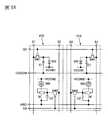
圖1是示出電子裝置的主要結構的一個例子的方塊圖。在圖1中,由箭頭連接的兩個組件以有線方式或無線方式電連接。另外,箭頭所示的方向表示輸出信號 的方向。FIG. 1 is a block diagram showing an example of the main structure of an electronic device. In Fig. 1, two components connected by arrows are electrically connected in a wired or wireless manner. In addition, the direction indicated by the arrow indicates the direction of the output signal.
本發明的一個方式的電子裝置包括顯示部15、攝像部16、控制部17、輸入部18以及檢測部19。該電子裝置也可以說是影像拍攝裝置、數位相機或數位攝影機。The electronic device according to one aspect of the present invention includes a display unit 15, an imaging unit 16, a control unit 17, an input unit 18, and a detection unit 19. The electronic device can also be said to be an image capturing device, a digital camera or a digital video camera.
顯示部15具有顯示圖像或影像的功能。攝像部16具有對被拍攝物件進行攝像的功能。控制部17具有控制顯示部15及攝像部16的工作的功能。The display unit 15 has a function of displaying images or videos. The imaging unit 16 has a function of imaging a subject. The control unit 17 has a function of controlling the operations of the display unit 15 and the imaging unit 16.
輸入部18具有將信號輸出到控制部17的功能。明確而言,輸入部18將用來使控制部17控制顯示部15及攝像部16的信號輸出到控制部17。使用者使用輸入部18操作電子裝置。The input unit 18 has a function of outputting a signal to the control unit 17. Specifically, the input unit 18 outputs a signal for the control unit 17 to control the display unit 15 and the imaging unit 16 to the control unit 17. The user uses the input unit 18 to operate the electronic device.
檢測部19具有將基於檢測部19所檢測出的外光照度的檢測資訊輸出到控制部17的功能。或者,檢測部19具有將檢測部19所檢測出的如使用者等被檢測物件的位置資訊輸出到控制部17的功能。由於電子裝置包括檢測部19,所以顯示部15能夠進行相應於使用環境的照度的顯示。The detection unit 19 has a function of outputting detection information based on the external light intensity detected by the detection unit 19 to the control unit 17. Alternatively, the detection unit 19 has a function of outputting the position information of a detected object such as a user detected by the detection unit 19 to the control unit 17. Since the electronic device includes the detection unit 19, the display unit 15 can display the illuminance corresponding to the use environment.
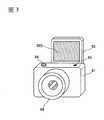
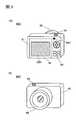
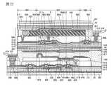
以下參照圖2A至圖3說明本發明的一個方式的電子裝置的具體結構例子。圖2A是電子裝置60A的背面側的立體圖,而圖2B及圖3是電子裝置60A的正面側的立體圖。Hereinafter, a specific configuration example of an electronic device according to one embodiment of the present invention will be described with reference to FIGS. 2A to 3. 2A is a perspective view of the back side of the
電子裝置60A包括外殼61、顯示裝置62、操作按鈕63、快門按鈕64、光感測器65、攝像部16以及控制部。另外,顯示裝置62包括顯示部62D。The
顯示部62D是圖1所示的顯示部15的一個例子。操作按鈕63及快門按鈕64是圖1所示的輸入部18的一個例子。光感測器65是圖1所示的檢測部19的一個例子。另外,在圖2A和圖2B中,未圖示對應於圖1所示的控制部17的控制部。The
顯示部62D設置在顯示裝置62中。顯示裝置62設置在外殼61的第一表面。就是說,顯示部62D設置在外殼61的第一表面(參照圖2A)。另外,鏡頭66設置在外殼61的與第一表面相對的第二表面(參照圖2B)。另外,光感測器65設置在外殼61的與第一表面及第二表面接觸的第三表面。快門按鈕64設置在第三表面。第三表面較佳為電子裝置60A的頂面。The
作為光感測器65,例如可以使用如光電二極體等光電轉換元件作為光的檢測部。光感測器65能夠根據流過光電轉換元件的電流量檢測出外光的照度。As the
攝像部16包括攝像元件及在攝像元件上成像的光學系統。作為攝像元件,例如可以使用電荷耦合裝置CCD或互補金屬氧化物半導體CMOS。另外,作為光學系統,除了鏡頭、光圈以外可以使用自動聚焦機構等。在圖2A和圖2A中,只示出攝像部16中的鏡頭66。The imaging unit 16 includes an imaging element and an optical system that forms an image on the imaging element. As the imaging element, for example, a charge coupled device CCD or a complementary metal oxide semiconductor CMOS can be used. In addition, as an optical system, in addition to a lens and an aperture, an autofocus mechanism or the like can be used. In FIGS. 2A and 2A, only the
操作按鈕63設置在外殼61的第一表面。使 用者可以使用操作按鈕63及快門按鈕64操作電子裝置60A。例如,藉由使用操作按鈕63,可以在顯示部62D上顯示靜態影像或動態影像或者設定曝光及放大等攝像條件等。另外,藉由使用快門按鈕64,可以對被拍攝物件調整焦距,並可以對被拍攝物件進行攝像等。The
另外,顯示裝置62隔著設置在與外殼61之間的可動部(未圖示)連接於外殼61。由於電子裝置60A具有可動部,所以可以將顯示裝置62抽出到背面側(第一表面一側)。另外,由於電子裝置60A具有可動部,所以可以使顯示裝置62成為使顯示部62D的顯示面朝向正面(第二表面一側)的狀態。圖3示出顯示部62D的顯示面朝向第二表面側的狀態下的電子裝置60A的正面側的立體圖。藉由在圖3的狀態下使用電子裝置60A,使用者能夠拍攝使用者本身的一部分(例如,臉、上半身等),亦即進行自拍。In addition, the
這裡,說明顯示部62D。Here, the
在顯示部62D中,反射可見光的第一顯示元件和發射可見光的第二顯示元件混合存在。In the
顯示部62D具有利用第一顯示元件所反射的第一光和第二顯示元件所發射的第二光中的一個或兩個顯示影像的功能。或者,顯示裝置具有藉由分別控制第一顯示元件所反射的第一光的光量和第二顯示元件所發射的第二光的光量來顯示灰階的功能。The
另外,顯示部62D較佳為包括藉由控制第一 顯示元件所反射的光的光量來顯示灰階的第一像素和藉由控制第二顯示元件所發射的光的光量來顯示灰階的第二像素。多個第一像素及多個第二像素分別配置為例如矩陣形狀,由此構成顯示部62D。In addition, the
另外,較佳為在顯示區域中以相同間距設置第一像素及第二像素。此時,可以將相鄰的第一像素和第二像素總稱為像素單元。In addition, it is preferable to arrange the first pixel and the second pixel at the same pitch in the display area. At this time, the adjacent first pixel and second pixel may be collectively referred to as a pixel unit.
再者,較佳為將第一像素及第二像素混合設置在顯示裝置的顯示區域中。由此,如下所述,可以在同一顯示區域中顯示只由多個第一像素顯示的影像、只由多個第二像素顯示的影像及由多個第一像素和多個第二像素的兩者顯示的影像。Furthermore, it is preferable to mix the first pixel and the second pixel in the display area of the display device. As a result, as described below, it is possible to display an image displayed only by a plurality of first pixels, an image displayed by only a plurality of second pixels, and two of a plurality of first pixels and a plurality of second pixels in the same display area. The image displayed by the person.
作為第一像素所包括的第一顯示元件,可以使用反射外光來進行顯示的元件。因為這種元件不包括光源,所以可以使顯示時的功耗變得極小。另外,當在如晴天下的屋外等外光的照度高的環境下使用電子裝置時,可以進行相應於該照度的高亮度顯示,由此可以進行高可見度的顯示。As the first display element included in the first pixel, an element that reflects external light for displaying can be used. Because this element does not include a light source, the power consumption during display can be extremely small. In addition, when the electronic device is used in an environment where the illuminance of external light is high, such as outdoors on a sunny day, a high-luminance display corresponding to the illuminance can be performed, thereby enabling a high-visibility display.
作為第一顯示元件,可以典型地使用反射型液晶元件。或者,作為第一顯示元件,不僅可以使用快門方式的MEMS(Micro Electro Mechanical Systems:微機電系統)元件、光干涉方式的MEMS元件,而且還可以使用應用微囊方式、電泳方式、電潤濕方式、電子粉流體(註冊商標)方式等的元件。As the first display element, a reflective liquid crystal element can be typically used. Alternatively, as the first display element, not only shutter-type MEMS (Micro Electro Mechanical Systems) elements and optical interference-type MEMS elements, but also microcapsule method, electrophoresis method, and electrowetting method can be used. , Electronic powder fluid (registered trademark) and other components.
另外,作為第二像素所包括的第二顯示元件,可以使用包括光源且利用來自該光源的光來進行顯示的元件。尤其是,較佳為使用藉由施加電場可以從發光物質取出光的電致發光元件。由於這種像素所發射的光的亮度及色度不受到外光的影響,因此這種像素可以進行色彩再現性高(色域寬)且對比度高的顯示,亦即鮮明的顯示。In addition, as the second display element included in the second pixel, an element that includes a light source and performs display using light from the light source can be used. In particular, it is preferable to use an electroluminescent element that can extract light from a luminescent substance by applying an electric field. Since the brightness and chromaticity of light emitted by such pixels are not affected by external light, such pixels can perform display with high color reproducibility (wide color gamut) and high contrast, that is, vivid display.
作為第二顯示元件,例如可以使用OLED(有機發光二極體)、LED(發光二極體)、QLED(Quantum-dot Light Emitting Diode:量子點發光二極體)等自發光性發光元件。或者,作為第二像素所包括的顯示元件,也可以組合作為光源的背光源和控制來自背光源的光的透光量的透射型液晶元件而使用。As the second display element, for example, self-luminous light-emitting elements such as OLED (Organic Light Emitting Diode), LED (Light Emitting Diode), QLED (Quantum-dot Light Emitting Diode), and the like can be used. Alternatively, as the display element included in the second pixel, a backlight as a light source may be used in combination with a transmissive liquid crystal element that controls the amount of light transmitted from the backlight.
例如,第一像素包括呈現白色(W)光的子像素、或者呈現紅色(R)光的子像素、呈現綠色(G)光的子像素及呈現藍色(B)光的子像素。另外,例如第二像素也同樣地包括呈現白色(W)光的子像素、或者呈現紅色(R)光的子像素、呈現綠色(G)光的子像素及呈現藍色(B)光的子像素。另外,第一像素及第二像素也可以分別包括四種顏色以上的子像素。子像素的種類越多,越可以降低功耗並提高色彩再現性。For example, the first pixel includes sub-pixels exhibiting white (W) light, or sub-pixels exhibiting red (R) light, sub-pixels exhibiting green (G) light, and sub-pixels exhibiting blue (B) light. In addition, for example, the second pixel also includes sub-pixels that exhibit white (W) light, or sub-pixels that exhibit red (R) light, sub-pixels that exhibit green (G) light, and sub-pixels that exhibit blue (B) light. Pixels. In addition, the first pixel and the second pixel may each include sub-pixels of four or more colors. The more types of sub-pixels, the more power consumption can be reduced and color reproducibility improved.
顯示部62D可以切換由第一像素顯示影像的第一顯示模式、由第二像素顯示影像的第二顯示模式及由第一像素和第二像素顯示影像的第三顯示模式。The
第一顯示模式是藉由利用第一顯示元件的反 射光顯示影像的模式。第一顯示模式是因不需要光源而實現極低功耗的驅動模式。例如,第一顯示模式在外光的照度充分高且外光為白色光或接近其的光的情況下是有效的。第一顯示模式例如是適合顯示書本或文件等的文字資訊的顯示模式。另外,因為使用反射光,所以可以進行保護眼睛的顯示,有不容易發生眼睛疲勞的效果。The first display mode is a mode for displaying images by using the reflected light of the first display element. The first display mode is a driving mode that achieves extremely low power consumption because it does not require a light source. For example, the first display mode is effective when the illuminance of the external light is sufficiently high and the external light is white light or light close thereto. The first display mode is, for example, a display mode suitable for displaying text information such as books or documents. In addition, because the reflected light is used, it can be displayed to protect the eyes, and has the effect of preventing eye fatigue.
第二顯示模式是藉由利用第二顯示元件的發光顯示影像的模式。由此,可以與外光的照度及色度無關地進行極鮮明(對比度高且色彩再現性高)的顯示。例如,第二顯示模式在夜間及昏暗的室內等的外光的照度極小的情況等下是有效的。另外,在外光昏暗時,明亮的顯示有時讓使用者感到刺眼。為了防止發生這種問題,在第二顯示模式中較佳為進行抑制亮度的顯示。由此,不僅可以抑制刺眼,而且還可以降低功耗。第二顯示模式是適合顯示鮮明的影像或流暢的動態影像的模式。The second display mode is a mode for displaying images by using the light emission of the second display element. As a result, it is possible to perform extremely vivid (high contrast and high color reproducibility) display regardless of the illuminance and chromaticity of external light. For example, the second display mode is effective when the illuminance of external light is extremely small at night or in a dark room. In addition, when the external light is dim, the bright display sometimes makes the user feel dazzling. In order to prevent such a problem from occurring, it is preferable to perform display with suppressed brightness in the second display mode. Thus, not only can the glare be suppressed, but also the power consumption can be reduced. The second display mode is a mode suitable for displaying vivid images or smooth moving images.
第三顯示模式是利用第一顯示元件的反射光和第二顯示元件的發光的兩者來進行顯示的模式。明確而言,以混合第一像素所呈現的光的顏色和與第一像素相鄰的第二像素所呈現的光的顏色來表示一個顏色的方式驅動顯示裝置。不但可以進行比第一顯示模式鮮明的顯示,而且而且可以使功耗比第二顯示模式小。例如,第三顯示模式在室內照明下或者早晨傍晚等外光照度較低的情況、外光的色度不是白色的情況等下是有效的。或者,在外光的照度高且外光的光源映射到顯示部(使用者會因顯示部的 表面反射而以視覺確認到外光的光源)的情況下,藉由以第三顯示模式提高亮度,可以提高可見度。The third display mode is a mode in which display is performed using both the reflected light of the first display element and the light emission of the second display element. Specifically, the display device is driven in a manner of mixing the color of light presented by the first pixel and the color of light presented by the second pixel adjacent to the first pixel to express one color. Not only can display more vividly than the first display mode, but also can make the power consumption smaller than the second display mode. For example, the third display mode is effective in situations where the external illuminance is low under indoor lighting or in the morning and evening, and when the chromaticity of external light is not white. Or, when the illuminance of the external light is high and the light source of the external light is mapped to the display part (the user can visually recognize the light source of the external light due to the reflection on the surface of the display part), the brightness is increased by using the third display mode, Can improve visibility.
在電子裝置60A中,光感測器65設置在外殼61的第三表面(參照圖2A和圖2B)。藉由對光感測器65所檢測出的照度設定臨界值,可以進行如下顯示:當光感測器65的檢測值為該臨界值以上時,顯示部62D以第一顯示模式進行顯示;當光感測器65的檢測值小於該臨界值時,顯示部62D以第二顯示模式進行顯示。電子裝置60A的上述驅動方法具有如下效果:當在明亮的環境下使用電子裝置60A時,能夠以顯示部62D的功耗低的方式進行高可見度及高亮度的顯示;當在黑暗的環境下使用電子裝置60A時,能夠以亮度低而不損害可見度的方式進行鮮豔的顯示。In the
上述臨界值較佳為300lux以上且20000lux以下,更佳為1000lux以上且15000lux以下,進一步較佳為5000lux以上且10000lux以下。The above-mentioned threshold is preferably 300 lux or more and 20000 lux or less, more preferably 1000 lux or more and 15000 lux or less, and still more preferably 5000 lux or more and 10000 lux or less.
另外,當檢測值為該臨界值以上時,顯示部62D也可以以第三顯示模式進行顯示。另外,光感測器65也可以不設置在第三表面而設置在第一表面或第二表面。另外,電子裝置60A也可以不包括光感測器65,而攝像部16代替具有檢測外光照度的功能。In addition, when the detection value is greater than or equal to the critical value, the
另外,藉由根據電子裝置60A的使用模式改變顯示部62D的顯示模式,可以降低電子裝置60A的功耗。例如,只在拍攝靜態影像的模式中調整焦距時以第三 顯示模式進行顯示,而在該模式中進行其他操作時或者在其他模式中以第一顯示模式進行顯示,由此可以降低電子裝置60A的功耗。另外,只在拍攝動態影像的模式中進行拍攝時以第三顯示模式進行顯示,而在該模式中進行其他操作時或者在其他模式中以第一顯示模式進行顯示,由此可以降低電子裝置60A的功耗。另外,只在使顯示部62D顯示所拍攝的靜態影像或動態影像以確認影像時以第三顯示模式進行顯示,而在其他模式中以第一顯示模式進行顯示,由此可以降低電子裝置60A的功耗。In addition, by changing the display mode of the
以下參照圖4A至圖5說明具有與電子裝置60A不同的結構的本發明的一個方式的電子裝置的具體結構例子。圖4A是電子裝置60B的背面側的立體圖,而圖4B及圖5是電子裝置60B的正面側的立體圖。Hereinafter, a specific configuration example of an electronic device of one embodiment of the present invention having a configuration different from that of the
電子裝置60B的與電子裝置60A不同之處為:使用光感測器65A及光感測器65B代替光感測器65。關於電子裝置60B的與電子裝置60A相同的結構可以參照上述電子裝置60A的說明。The difference between the
光感測器65A設置在外殼61的第一表面,而光感測器65B設置在外殼61的第二表面(參照圖4A和圖4B)。光感測器65A及光感測器65B可以採用與光感測器65相同的結構。The
藉由使用具有這種結構的電子裝置60B,可 以比較電子裝置60B的背面側的外光亮度,亦即光感測器65A所檢測出的照度(以下也稱為第一照度)和電子裝置60B的正面側的外光亮度,亦即光感測器65B所檢測出的照度(以下也稱為第二照度),由此根據第一照度和第二照度的大小關係改變顯示部62D的顯示模式。By using the
明確而言,可以進行如下顯示:當第一照度大於第二照度時,顯示部62D以第三顯示模式進行顯示;當第一照度小於第二照度時,顯示部62D以第一顯示模式或第二顯示模式進行顯示(以下將這種顯示設定稱為第一設定模式)。當以第一設定模式驅動電子裝置60B時,在電子裝置60B為圖5的狀態且外光的光源位於外殼61的背面側(例如,在順光的光線狀態下進行自拍)的情況下,使用者可以在看到亮度高且可見度高的顯示的狀態下進行拍攝。Specifically, the following display can be performed: when the first illuminance is greater than the second illuminance, the
另外,也可以進行如下顯示:當第一照度小於第二照度時,顯示部62D以第三顯示模式進行顯示;當第一照度大於第二照度時,顯示部62D以第一顯示模式或第二顯示模式進行顯示(以下將這種顯示設定稱為第二設定模式)。當以第二設定模式驅動電子裝置60B時,在電子裝置60B為圖4A的狀態且外光的光源位於外殼61的正面側(例如,在逆光的光線狀態下拍攝位於外殼61的正面側的被拍攝物件)的情況下,使用者可以在看到亮度高且可見度高的顯示的狀態下進行拍攝。In addition, the following display can also be performed: when the first illuminance is less than the second illuminance, the
因此,例如,在電子裝置60B為圖5的狀態 (亦即,顯示部62D的顯示面朝向第二表面一側的狀態)下以第一設定模式驅動電子裝置60B,而在電子裝置60B為圖4A的狀態(亦即,顯示部62D的顯示面朝向第一表面一側的狀態)下以第二設定模式驅動電子裝置60B,由此在各種各樣的拍攝情況下,使用者可以在看到亮度高且可見度高的顯示的狀態下進行拍攝。Therefore, for example, when the
在本說明書中,順光的光線狀態是指;在將被拍攝物件與電子裝置的第二表面彼此相對的表面設定為它們的正面的情況下,外光的光源位於被拍攝物件的正面側及電子裝置的背面側的狀態。另外,逆光的光線狀態是指:在將被拍攝物件與電子裝置的第二表面彼此相對的表面設定為它們的正面的情況下,外光的光源位於被拍攝物件的背面側及電子裝置的正面側的狀態。In this specification, the light state of the forward light means; when the surface of the object to be photographed and the second surface of the electronic device opposite to each other is set as their front, the light source of the external light is located on the front side of the object to be photographed and The state of the back side of the electronic device. In addition, the light state of the backlight means that when the surface of the object to be photographed and the second surface of the electronic device are set as their fronts, the light source of external light is located on the back side of the object to be photographed and the front of the electronic device. The state of the side.
以下參照圖6A至圖7B2說明具有與電子裝置60A不同的結構的本發明的一個方式的電子裝置的具體結構例子。圖6A是電子裝置60C的背面側的立體圖,而圖6B是電子裝置60C的正面側的立體圖。Hereinafter, a specific configuration example of an electronic device of one embodiment of the present invention having a configuration different from that of the
電子裝置60C的與電子裝置60A不同之處為:使用位置感測器65C代替光感測器65。關於電子裝置60C的與電子裝置60A相同的結構可以參照上述電子裝置60A的說明。The difference between the
位置感測器65C是圖1所示的檢測部19的一 個例子。The
在電子裝置60C中,位置感測器65C設置在外殼61的第一表面(參照圖6A)。藉由設定位置感測器65C能夠檢測出被檢測物件的區域的距離及角度,可以進行如下顯示:當位置感測器65C檢測出使用者時,顯示部62D以第一顯示模式進行顯示;當位置感測器65C檢測不出使用者時,顯示部62D以第三顯示模式進行顯示。電子裝置60C的上述驅動方法具有如下效果:當電子裝置60C為圖6A的狀態且外光的光源位於外殼61的背面側(例如,在順光的光線狀態下拍攝位於電子裝置60C的正面側的被拍攝物件)時,無論使用者保持電子裝置60C的位置及角度如何都能顯示可見度高的顯示。In the
作為位置感測器65C,可以使用電荷耦合裝置(CCD)或互補金屬氧化物半導體(CMOS)感測器等檢測出可見光的元件。或者,也可以使用紅外線感測器、超聲波感測器等。藉由使用設置在外殼61的第一表面的位置感測器65C,可以檢測出電子裝置60C的使用者的位置資訊。例如,當使用者與外殼61的第一表面相對時,位置感測器65C檢測出使用者,當使用者不與外殼61的第一表面相對時,位置感測器65C檢測不出使用者。As the
圖7A1、圖7A2、圖7B1以及圖7B2是示出使用電子裝置60C時的使用者與電子裝置60C的位置關係的示意圖。圖7A1是使用者67的身體方向與電子裝置60C的拍攝方向(圖7A1所示的箭頭X)大致平行時的俯視 圖,而圖7B1是電子裝置60C的拍攝方向在一定程度上傾斜於使用者67的身體方向時的俯視圖。圖7A2和圖7B2分別是對應於圖7A1和圖7B1的位置關係的側面圖。在圖7A1、圖7A2、圖7B1以及圖7B2中,假設為使用者在屋外使用電子裝置60C,且未圖示的外光的光源,例如太陽位於使用者67的背面側。在圖7A1、圖7A2、圖7B1以及圖7B2中,省略示出使用者67保持電子裝置60C的手。7A1, FIG. 7A2, FIG. 7B1, and FIG. 7B2 are schematic diagrams showing the positional relationship between the user and the
圖7A1、圖7A2、圖7B1以及圖7B2中的區域68表示位置感測器65C能夠檢測出被檢測物件的範圍(以下也稱為檢測範圍)。檢測範圍可以被垂直於第一表面的方向上的從位置感測器65C的距離d及角度ω定義(參照圖7A1及圖7A2)。The
在圖7A1及圖7A2的狀態下,使用者67成為遮蔽物,由此抑制光源映射到顯示部62D(使用者67因顯示部62D的表面反射而看到光源)。在此狀態下,因為使用者67的頭部67H在檢測範圍內,由此位置感測器65C檢測出被檢測物件,亦即使用者67,使得顯示部62D以第一顯示模式進行顯示。In the state of FIGS. 7A1 and 7A2, the
另一方面,在圖7B1及圖7B2的狀態下,伴隨光源的位置,使用者67有時不成為遮蔽物,由此光源映射到顯示部62D。圖7B1示出來自光源的光69因被顯示部62D的表面反射而被使用者67看到的狀態。在此狀態下,因為使用者67在檢測範圍外,由此位置感測器 65C檢測不出被檢測物件,亦即使用者67,使得顯示部62D以第三顯示模式進行顯示。On the other hand, in the state of FIGS. 7B1 and 7B2, the
如上所述,當發生光源的映射時以第三顯示模式進行亮度高且可見度高的顯示,當沒發生光源的映射時以第一顯示模式進行功耗低的顯示,由此可以抑制電子裝置60C的功耗,並且無論使用者保持電子裝置60C的位置及角度如何都能顯示可見度高的顯示。As described above, when light source mapping occurs, high-brightness and high visibility display is performed in the third display mode, and low power consumption display is performed in the first display mode when light source mapping does not occur, thereby suppressing the
藉由將圖7A1和圖7A2所示的角度ω及距離d設定為適當的數值,可以根據位置感測器65C的檢測狀態改變顯示模式。例如,角度ω較佳為1°以上且20°以下,更佳為3°以上且10°以下。距離d較佳為100mm以上且500mm以下,更佳為150mm以上且300mm以下。By setting the angle ω and the distance d shown in FIGS. 7A1 and 7A2 to appropriate values, the display mode can be changed according to the detection state of the
本實施方式的至少一部分可以與本說明書所記載的其他實施方式適當地組合而實施。At least a part of this embodiment can be implemented in appropriate combination with other embodiments described in this specification.
在本實施方式中,參照圖式對實施方式1所示的顯示裝置62的更具體的結構例子進行說明。In this embodiment, a more specific configuration example of the
圖8示出顯示裝置62的方塊圖。顯示裝置62具有顯示部62D。FIG. 8 shows a block diagram of the
顯示部62D包括設置為矩陣狀的多個像素單元30。像素單元30包括第一像素31p和第二像素32p。The
圖8示出第一像素31p和第二像素32p都包括對應於紅色(R)、綠色(G)、藍色(B)的三種顏色的顯示元件的情況的例子。FIG. 8 shows an example of a case where both the
第一像素31p包括對應於紅色(R)的顯示元件31R、對應於綠色(G)的顯示元件31G、對應於藍色(B)的顯示元件31B。顯示元件31R、31G、31B都是利用外光的反射的顯示元件。The
第二像素32p包括對應於紅色(R)的顯示元件32R、對應於綠色(G)的顯示元件32G、對應於藍色(B)的顯示元件32B。顯示元件32R、32G、32B都是利用光源的光的顯示元件。The
圖9A至圖9C是示出像素單元30的結構例子的示意圖。圖9A至圖9C所示的像素單元30包括第一像素31p和第二像素32p。9A to 9C are schematic diagrams showing structural examples of the
第一像素31p包括顯示元件31R、顯示元件31G、顯示元件31B。顯示元件31R、顯示元件31G及顯示元件31B都是反射外光而進行顯示的元件。顯示元件31R反射外光,並將紅色的光Rr射出到顯示面一側。與此同樣,顯示元件31G、顯示元件31B也分別將綠色光Gr、藍色光Br射出到顯示面一側。The
第二像素32p包括顯示元件32R、顯示元件32G及顯示元件32B。顯示元件32R、顯示元件32G及顯 示元件32B都是發光元件。顯示元件32R將紅色光Rt射出到顯示面一側。與此同樣,顯示元件32G、顯示元件32B也分別將綠色光Gt、藍色光Bt射出到顯示面一側。由此,可以以低功耗進行鮮明的顯示。The
圖9A對應於藉由驅動第一像素31p和第二像素32p的兩者來進行顯示的模式(第三顯示模式)。在像素單元30中,藉由混合光Rr、光Gr、光Br、光Rt、光Gt及光Bt的六個光的顏色,可以將混合有反射光和透射光的規定的顏色的光35tr射出到顯示面一側。FIG. 9A corresponds to a mode (third display mode) in which display is performed by driving both of the
此時,用來使光35tr具有規定的亮度及色度的光Rr、光Gr、光Br、光Rt、光Gt及光Bt的六個光的亮度有多種組合。於是,在本發明的一個方式中,在用來實現一個亮度及色度的光35tr的六個光的亮度(灰階)的組合中,較佳為選擇使從第一像素31p射出的光Rr、光Gr及光Br的亮度(灰階)成為最大的組合。由此,可以降低功耗而無需犧牲顏色再現性。At this time, there are various combinations of the brightness of the six lights of light Rr, light Gr, light Br, light Rt, light Gt, and light Bt for making the light 35tr have predetermined brightness and chromaticity. Therefore, in one aspect of the present invention, it is preferable to select the light Rr emitted from the
圖9B對應於藉由驅動第一像素31p只使用反射光進行顯示的模式(第一顯示模式)。在像素單元30中,例如在外光的照度充分高的情況等下,只混合來自第一像素31p的光(光Rr、光Gr及光Br)而不驅動第二像素32p,由此可以將組合反射光的規定的顏色的光35r射出到顯示面一側。由此,可以進行功耗極低的驅動。另外,可以進行對眼睛刺激少的顯示。FIG. 9B corresponds to a mode (first display mode) in which only reflected light is used for display by driving the
圖9C對應於藉由驅動第二像素32p只使用發 光(透射光)進行顯示的模式(第二顯示模式)。在像素單元30中,例如在外光的照度極小的情況等下,只混合來自第二像素32p的光(光Rt、光Gt及光Bt)而不驅動第一像素31p,由此可以將規定的顏色的光35t射出到顯示面一側。由此,可以進行鮮明的顯示。另外,藉由在外光的照度小的情況下降低亮度,可以在抑制使用者所感到的刺眼的同時降低功耗。Fig. 9C corresponds to a mode (second display mode) in which only light emission (transmitted light) is used for display by driving the
在上述說明中示出第一像素31p和第二像素32p都包括對應於紅色(R)、綠色(G)、藍色(B)的三種顏色的顯示元件的例子,但是不侷限於此。以下示出與上述說明不同的結構例子。The above description shows an example in which both the
圖10A至圖10C、圖11A至圖11C示出像素單元30的結構例子。注意,雖然在此示出與藉由驅動第一像素31p和第二像素32p的兩者來進行顯示的模式(第三顯示模式)對應的示意圖,但是與上述說明同樣,也可以以藉由驅動第一像素31p只使用反射光進行顯示的模式(第一顯示模式)及藉由驅動第二像素32p只使用發光(透射光)進行顯示的模式(第二顯示模式)來進行顯示。10A to 10C and 11A to 11C show structural examples of the
圖10A示出第二像素32p除了包括顯示元件32R、顯示元件32G、顯示元件32B之外還包括呈現白色(W)的顯示元件32W的例子。由此,可以降低使用第二像素32p的顯示模式(第二顯示模式及第三顯示模式)所需要 的功耗。FIG. 10A shows an example in which the
圖10B示出第二像素32p除了包括顯示元件32R、顯示元件32G、顯示元件32B之外還包括呈現黃色(Y)的顯示元件32Y的例子。由此,可以降低使用第二像素32p的顯示模式(第二顯示模式及第三顯示模式)所需要的功耗。FIG. 10B shows an example in which the
圖10C示出第一像素31p除了包括顯示元件31R、顯示元件31G、顯示元件31B之外還包括呈現白色(W)的顯示元件31W的例子。再者,圖10C示出第二像素32p除了包括顯示元件32R、顯示元件32G、顯示元件32B之外還包括呈現白色(W)的顯示元件32W的例子。由此,可以降低使用第一像素31p的顯示模式(第一顯示模式及第三顯示模式)及使用第二像素32p的顯示模式(第二顯示模式及第三顯示模式)所需要的功耗。FIG. 10C shows an example in which the
圖11A示出第一像素31p只包括呈現白色的顯示元件31W的例子。此時,在只使用第一像素31p的顯示模式(第一顯示模式)中,可以進行黑白顯示或灰階顯示,在使用第二像素32p的顯示模式(第二顯示模式及第三顯示模式)中,可以進行彩色顯示。FIG. 11A shows an example in which the
另外,藉由採用這種結構,可以提高第一像素31p的開口率,所以可以提高第一像素31p的反射率,而顯示更明亮的影像。In addition, by adopting this structure, the aperture ratio of the
圖11B示出第二像素32p除了包括圖11A所示的顯示元件32R、顯示元件32G、顯示元件32B之外還 包括呈現白色(W)的顯示元件32W的例子。由此,可以降低使用第二像素32p的顯示模式(第二顯示模式及第三顯示模式)所需要的功耗。Fig. 11B shows an example in which the
圖11C示出第二像素32p除了包括圖11A所示的顯示元件32R、顯示元件32G、顯示元件32B之外還包括呈現黃色(Y)的顯示元件32Y的例子。由此,可以降低使用第二像素32p的顯示模式(第二顯示模式及第三顯示模式)所需要的功耗。FIG. 11C shows an example in which the
以上是顯示單元的結構例子的說明。The above is the description of the structural example of the display unit.
圖12示出顯示裝置62中的顯示部62D的剖面結構的一個例子。FIG. 12 shows an example of the cross-sectional structure of the
顯示裝置62在基板11與基板12之間包括:第一層41;絕緣層134;絕緣層135;顯示元件32;黏合層151;第二層42;絕緣層234;以及顯示元件31等。The
顯示元件31包括導電層221、導電層223及它們之間的液晶222。導電層221反射可見光,導電層223透射可見光。因此,顯示元件31是將反射光22射出到基板12一側的反射型液晶元件。在此,導電層221配置在各像素中,並被用作像素電極。導電層223橫跨配置在多個像素中。導電層223在未圖示的區域中與被供應恆定電位的佈線連接,並被用作共用電極。The
顯示元件32包括導電層121、導電層123及 它們之間的EL層122。EL層122是至少包含發光物質的層。導電層121反射可見光,導電層123透射可見光。因此,顯示元件32是藉由在導電層121與導電層123之間施加電壓將光21射出到基板12一側的電致發光元件。導電層121配置在各像素中,並被用作像素電極。EL層122和導電層123橫跨配置在多個像素中。導電層123在未圖示的區域中與被供應恆定電位的佈線連接,並被用作共用電極。The
第一層41是包括驅動顯示元件31的電路的層。第二層42是包括驅動顯示元件32的電路的層。例如,在第一層41及第二層42中,由電晶體、電容器、佈線、電極等構成像素電路。The
在第一層41與導電層221之間設置有絕緣層234。另外,導電層221與第一層41藉由形成在絕緣層234中的開口電連接,由此,第一層41與顯示元件31電連接。An insulating
在第二層42與導電層121之間設置有絕緣層134。另外,導電層121與第二層42藉由形成在絕緣層134中的開口電連接,由此第二層42與顯示元件32電連接。An insulating
使用黏合層151將第一層41與導電層123貼合。黏合層151也被用作密封顯示元件32的密封層。The
在此,在將使用氧化物半導體的關態電流極低的電晶體用於第一層41的像素電路、或者將記憶元件 用於該像素電路的情況等下,即使在使用顯示元件31顯示靜態影像時停止對像素的寫入工作,也可以保持灰階。就是說,即使使圖框頻率極小也可以持續進行顯示。因為在本發明的一個方式中設置有屏蔽雜訊的導電層123,所以可以抑制由雜訊導致的顯示元件31的灰階的變動。由此,可以在保持顯示品質的同時使圖框頻率變得極小,而可以進行低功耗的驅動。Here, in the case where a transistor with extremely low off-state current using an oxide semiconductor is used for the pixel circuit of the
以上是對顯示裝部的剖面結構例子的說明。The above is the description of the cross-sectional structure example of the display unit.
本實施方式的至少一部分可以與本說明書所記載的其他實施方式適當地組合而實施。At least a part of this embodiment can be implemented in appropriate combination with other embodiments described in this specification.
在本實施方式中,對本發明的一個方式的顯示裝置的基本結構進行說明。In this embodiment, the basic configuration of a display device according to an aspect of the present invention will be described.
實施方式1所示的顯示裝置62的一個方式具有設置有包括反射型液晶元件的第一像素的第一顯示面板與設置有包括發光元件的第二像素的第二顯示面板藉由黏合層貼合在一起的結構。反射型液晶元件可以藉由控制反射光的光量表示灰階。發光元件可以藉由控制發射光的光量表示灰階。One aspect of the
顯示裝置例如可以只利用反射光進行顯示,也可以只利用來自發光元件的光進行顯示,還可以利用反射光及來自發光元件的光的兩者進行顯示。For example, the display device may perform display using only reflected light, may perform display using only light from a light emitting element, or may perform display using both reflected light and light from the light emitting element.
第一顯示面板設置在觀看側,第二顯示面板 設置在與觀看側相反的一側。第一顯示面板包括位於最靠近黏合層一側的第一樹脂層。第二顯示面板包括位於最靠近黏合層一側的第二樹脂層。The first display panel is arranged on the viewing side, and the second display panel is arranged on the side opposite to the viewing side. The first display panel includes a first resin layer on the side closest to the adhesive layer. The second display panel includes a second resin layer on the side closest to the adhesive layer.
另外,較佳的是,在第一顯示面板的顯示面一側設置第三樹脂層,在第二顯示面板的背面一側(與顯示面相反的一側)設置第四樹脂層。由此,可以實現極輕且不容易破損的顯示裝置。In addition, it is preferable that the third resin layer is provided on the display surface side of the first display panel, and the fourth resin layer is provided on the back side (the side opposite to the display surface) of the second display panel. As a result, a display device that is extremely light and not easily damaged can be realized.
第一樹脂層至第四樹脂層(以下也總稱為樹脂層)具有極薄的特徵。明確而言,其厚度較佳為0.1μm以上且3μm以下。由此,即使層疊兩個顯示面板,也可以使其厚度很薄。另外,可以抑制位於第二像素的發光元件所發射的光的路徑上的樹脂層對光的吸收,因此可以高效地提取光並降低功耗。The first to fourth resin layers (hereinafter also collectively referred to as resin layers) have a feature of being extremely thin. Specifically, the thickness is preferably 0.1 μm or more and 3 μm or less. Thus, even if two display panels are laminated, the thickness can be made thin. In addition, it is possible to suppress the absorption of light by the resin layer located on the path of the light emitted by the light-emitting element of the second pixel, so it is possible to efficiently extract light and reduce power consumption.
樹脂層例如可以使用如下方式形成。在支撐基板上塗佈低黏度的熱固性樹脂材料,進行熱處理使其硬化來形成樹脂層。接著,在樹脂層上形成結構體。然後,在樹脂層與支撐基板之間進行剝離,以使樹脂層的一個表面露出。The resin layer can be formed in the following manner, for example. A low-viscosity thermosetting resin material is coated on the support substrate and heat-treated to harden to form a resin layer. Next, a structure is formed on the resin layer. Then, peeling is performed between the resin layer and the supporting substrate to expose one surface of the resin layer.
在剝離支撐基板與樹脂層時,作為降低彼此之間的黏合性的方法,可以舉出照射雷射的方法。例如,較佳的是,作為雷射利用線狀雷射,掃描該雷射來照射雷射。由此,可以縮短支撐基板面積大時的製程時間。作為雷射,較佳為使用波長為308nm的準分子雷射。When peeling the support substrate and the resin layer, as a method of reducing the adhesion between each other, a method of irradiating a laser can be cited. For example, it is preferable to use a linear laser as the laser, and scan the laser to irradiate the laser. As a result, the process time when the supporting substrate area is large can be shortened. As the laser, it is preferable to use an excimer laser with a wavelength of 308 nm.
作為能夠用於樹脂層的材料,典型地可以舉 出熱固性聚醯亞胺。尤其是,較佳為使用感光性聚醯亞胺。感光性聚醯亞胺是適用於顯示面板的平坦化膜等的材料,因此可以利用已有的形成設備及材料。由此,不需要用於實現本發明的一個方式的結構的新的設備及材料。As a material that can be used for the resin layer, a thermosetting polyimide is typically cited. In particular, it is preferable to use photosensitive polyimide. Photosensitive polyimide is a material suitable for flattening films of display panels and the like, so existing forming equipment and materials can be used. Therefore, new equipment and materials for realizing the structure of one aspect of the present invention are not required.
另外,當作為樹脂層使用感光性樹脂材料時,藉由進行曝光及顯影處理,可以對樹脂層進行加工。例如,可以形成開口,並可以去除不需要的部分。另外,藉由對曝光方法及曝光條件實施最佳化,可以在其表面形成凹凸形狀。例如,可以採用使用半色調遮罩或灰色調遮罩的曝光技術或者多重曝光技術等。In addition, when a photosensitive resin material is used as the resin layer, the resin layer can be processed by performing exposure and development treatments. For example, an opening can be formed, and unnecessary parts can be removed. In addition, by optimizing the exposure method and exposure conditions, it is possible to form uneven shapes on the surface. For example, an exposure technique using a halftone mask or a gray tone mask or a multiple exposure technique can be used.
另外,也可以使用非感光性樹脂材料。此時,可以採用在樹脂層上形成光阻遮罩或硬質遮罩以形成開口或凹凸形狀的方法。In addition, non-photosensitive resin materials can also be used. At this time, a method of forming a photoresist mask or a hard mask on the resin layer to form an opening or a concave-convex shape can be adopted.
在此,較佳為部分地去除位於來自發光元件的光的路徑上的樹脂層。也就是說,在第一樹脂層及第二樹脂層中形成與發光元件重疊的開口。由此,可以抑制因來自發光元件的光的一部分被樹脂層吸收而導致的顏色再現性降低及光提取效率下降。Here, it is preferable to partially remove the resin layer located on the path of the light from the light emitting element. That is, openings overlapping with the light-emitting element are formed in the first resin layer and the second resin layer. Thereby, it is possible to suppress a decrease in color reproducibility and a decrease in light extraction efficiency due to part of the light from the light emitting element being absorbed by the resin layer.
或者,可以以樹脂層中的位於來自發光元件的光的路徑上的部分薄於其他部分的方式在樹脂層中形成凹部。也就是說,樹脂層可以具有厚度不同的兩個部分,並且厚度薄的部分重疊於發光元件。當採用該結構時,也可以減小樹脂層對來自發光元件的光的吸收。Alternatively, the concave portion may be formed in the resin layer in such a manner that the portion of the resin layer located on the path of the light from the light-emitting element is thinner than other portions. That is, the resin layer may have two parts with different thicknesses, and the part with a thin thickness overlaps the light-emitting element. When this structure is adopted, the absorption of light from the light-emitting element by the resin layer can also be reduced.
另外,在第一顯示面板包括第三樹脂層的情 況下,與上述同樣地,較佳為形成與發光元件重疊的開口。由此,可以進一步提高顏色再現性及光提取效率。In addition, in the case where the first display panel includes the third resin layer, similar to the above, it is preferable to form an opening overlapping the light-emitting element. As a result, color reproducibility and light extraction efficiency can be further improved.
另外,在第一顯示面板包括第三樹脂層的情況下,較佳為去除位於反射型液晶元件的光的路徑上的第三樹脂層的一部分。也就是說,在第三樹脂層中形成與反射型液晶元件重疊的開口。由此,可以提高反射型液晶元件的反射率。In addition, in the case where the first display panel includes the third resin layer, it is preferable to remove a part of the third resin layer located on the path of the light of the reflective liquid crystal element. That is, an opening overlapping with the reflective liquid crystal element is formed in the third resin layer. As a result, the reflectance of the reflective liquid crystal element can be improved.
當在樹脂層中形成開口時,在支撐基板上形成光吸收層,在該光吸收層上形成具有開口的樹脂層,並且形成覆蓋開口的透光層。光吸收層是藉由吸收光被加熱來釋放氫或氧等的氣體的層。因此,藉由從支撐基板一側照射光使光吸收層釋放氣體,可以降低光吸收層與支撐基板之間的介面或光吸收層與透光層之間的黏合性而進行剝離。或者,可以使光吸收層本身產生斷裂而進行剝離。When the opening is formed in the resin layer, a light absorption layer is formed on the support substrate, a resin layer having an opening is formed on the light absorption layer, and a light-transmitting layer covering the opening is formed. The light-absorbing layer is a layer that is heated by absorbing light to release gases such as hydrogen or oxygen. Therefore, by irradiating light from the side of the supporting substrate to release gas from the light-absorbing layer, the interface between the light-absorbing layer and the supporting substrate or the adhesion between the light-absorbing layer and the light-transmitting layer can be reduced for peeling. Alternatively, the light absorbing layer itself may be broken and peeled off.
或者,也可以使用如下方法。將樹脂層中的成為開口的部分形成得較薄,藉由上述方法剝離支撐基板與樹脂層。然後,對樹脂層的剝離表面進行電漿處理等減薄樹脂層的厚度,由此可以在樹脂層的較薄部分形成開口。Alternatively, the following method can also be used. The part that becomes the opening in the resin layer is formed thinner, and the supporting substrate and the resin layer are peeled off by the above-mentioned method. Then, the peeled surface of the resin layer is subjected to plasma treatment or the like to reduce the thickness of the resin layer, thereby forming an opening in the thin portion of the resin layer.
另外,第一像素及第二像素較佳為都包括電晶體。作為形成該電晶體的通道的半導體,較佳為使用氧化物半導體。當採用氧化物半導體時,即使降低電晶體的製程中的最高溫度(例如,降低到400℃以下,較佳為350℃以下),也可以實現高通態電流,並可以獲得高可靠 性。另外,當使用氧化物半導體時,用於位於電晶體的被形成面一側的樹脂層的材料不要求高耐熱性,所以可以擴大材料的選擇範圍。例如,也可以使用用於平坦化膜的樹脂材料。In addition, both the first pixel and the second pixel preferably include transistors. As the semiconductor forming the channel of the transistor, an oxide semiconductor is preferably used. When an oxide semiconductor is used, even if the maximum temperature in the manufacturing process of the transistor is lowered (for example, lowered to below 400°C, preferably below 350°C), high on-state current can be achieved and high reliability can be obtained. In addition, when an oxide semiconductor is used, the material used for the resin layer on the side of the surface to be formed of the transistor does not require high heat resistance, so the selection range of materials can be expanded. For example, a resin material used for the planarization film can also be used.
在此,在使用低溫多晶矽(LTPS:Low Temperature Poly-Silicon)的情況下,雖然能夠得到高場效移動率,但是需要進行雷射晶化處理、晶化處理之前的預烤製程、使雜質元素啟動的烘烤製程等,在電晶體製程中的最高溫度比使用上述氧化物半導體時較高(例如,500℃以上、550℃以上或600℃以上)。因此,位於電晶體的被形成面一側的樹脂層需要具有高耐熱性。再者,在雷射晶化製程中,該樹脂層被照射雷射,因此需要將該樹脂層的厚度形成得較厚(例如,10μm以上或20μm以上)。Here, in the case of using low temperature polysilicon (LTPS: Low Temperature Poly-Silicon), although high field efficiency mobility can be obtained, laser crystallization treatment, pre-baking process before crystallization treatment, and impurity elements are required. For the firing process to be started, the maximum temperature in the transistor process is higher than when the above-mentioned oxide semiconductor is used (for example, 500°C or higher, 550°C or higher, or 600°C or higher). Therefore, the resin layer on the side of the formed surface of the transistor needs to have high heat resistance. Furthermore, in the laser crystallization process, the resin layer is irradiated with laser, so the thickness of the resin layer needs to be thicker (for example, 10 μm or more or 20 μm or more).
另一方面,在使用氧化物半導體的情況下,不需要特殊的耐熱性高的材料,並且可以形成得較薄,因此可以降低在顯示面板整體中該樹脂層的成本比率。On the other hand, when an oxide semiconductor is used, a special material with high heat resistance is not required and can be formed thinner, so the cost ratio of the resin layer in the entire display panel can be reduced.
氧化物半導體具有寬能帶間隙(例如,2.5eV以上或3.0eV以上)並具有透光性。因此,在剝離支撐基板與樹脂層的製程中,即使雷射照射到氧化物半導體也不容易被吸收,所以可以抑制對氧化物半導體的電特性帶來的影響。因此,如上所述那樣可以將樹脂層形成得薄。The oxide semiconductor has a wide band gap (for example, 2.5 eV or more or 3.0 eV or more) and has light transmittance. Therefore, in the process of peeling the support substrate and the resin layer, even if the laser is irradiated to the oxide semiconductor, it is not easily absorbed, so the influence on the electrical characteristics of the oxide semiconductor can be suppressed. Therefore, the resin layer can be formed thin as described above.
本發明的一個方式藉由組合使用以感光性聚醯亞胺為代表的低黏度感光性樹脂材料而形成的薄樹脂層以及即使在低溫度環境下也能夠實現電特性優異的電晶體 的氧化物半導體來可以實現生產率非常高的顯示裝置。One aspect of the present invention is a combination of a thin resin layer formed by using a low-viscosity photosensitive resin material represented by photosensitive polyimide, and an oxide capable of realizing a transistor with excellent electrical properties even in a low-temperature environment A display device with very high productivity can be realized by semiconductors.
接著,對像素結構進行說明。多個第一像素及多個第二像素分別配置為矩陣形狀而構成顯示部。另外,顯示裝置較佳為包括驅動第一像素的第一驅動部及驅動第二像素的第二驅動部。第一驅動部及第二驅動部較佳為分別設置在第一顯示面板及第二顯示面板中。Next, the pixel structure will be described. The plurality of first pixels and the plurality of second pixels are respectively arranged in a matrix shape to form a display portion. In addition, the display device preferably includes a first driving unit for driving the first pixel and a second driving unit for driving the second pixel. The first driving part and the second driving part are preferably provided in the first display panel and the second display panel, respectively.
另外,第一像素及第二像素較佳為以相同的週期配置在顯示區域內。並且,第一像素及第二像素較佳為混合配置在顯示裝置的顯示區域中。由此,如後面所述,可以將只有多個第一像素所顯示的影像、只有多個第二像素所顯示的影像以及多個第一像素和多個第二像素兩者所顯示的影像分別都顯示在相同的顯示區域中。In addition, the first pixel and the second pixel are preferably arranged in the display area with the same period. In addition, the first pixel and the second pixel are preferably mixedly arranged in the display area of the display device. Thus, as described later, it is possible to separate the images displayed by only a plurality of first pixels, images displayed by only a plurality of second pixels, and images displayed by both the plurality of first pixels and the plurality of second pixels. Both are displayed in the same display area.
在此,第一像素例如較佳為由呈現白色(W)的一個像素構成。第二像素例如較佳為包括分別呈現紅色(R)、綠色(G)、藍色(B)這三種顏色的光的子像素。除此之外,還可以包括呈現白色(W)或黃色(Y)的光的子像素。當這種第一像素及第二像素以相同的週期配置時,可以增大第一像素的面積而提高第一像素的開口率。Here, the first pixel is preferably composed of, for example, one pixel that appears white (W). For example, the second pixel preferably includes sub-pixels that respectively present three colors of red (R), green (G), and blue (B). In addition to this, it may also include sub-pixels that exhibit white (W) or yellow (Y) light. When the first pixel and the second pixel are arranged in the same period, the area of the first pixel can be increased to increase the aperture ratio of the first pixel.
另外,第一像素例如也可以包括分別呈現紅色(R)、綠色(G)、藍色(B)這三種顏色的光的子像素,除此之外,還可以包括呈現白色(W)或黃色(Y)的光的子像素。In addition, the first pixel may include, for example, sub-pixels that respectively present three colors of red (R), green (G), and blue (B). In addition, it may also include sub-pixels that present white (W) or yellow. (Y) Light sub-pixel.
接著,對能夠用於第一顯示面板及第二顯示面板的電晶體進行說明。設置在第一顯示面板的第一像素中的電晶體與設置在第二顯示面板的第二像素中的電晶體 既可以具有相同的結構,又可以具有不同的結構。Next, the transistors that can be used for the first display panel and the second display panel will be described. The transistor provided in the first pixel of the first display panel and the transistor provided in the second pixel of the second display panel may have the same structure or different structures.
作為電晶體的結構,例如可以舉出底閘極結構的電晶體。底閘極結構的電晶體在半導體層的下方(被形成面一側)具有閘極電極。另外,例如,其源極電極及汲極電極與半導體層的頂面及側端部接觸。As the structure of the transistor, for example, a transistor with a bottom gate structure can be cited. The transistor of the bottom gate structure has a gate electrode under the semiconductor layer (on the side of the formed surface). In addition, for example, the source electrode and the drain electrode are in contact with the top surface and the side end of the semiconductor layer.
另外,作為電晶體的其他結構,例如可以舉出頂閘極結構的電晶體。頂閘極結構的電晶體在半導體層的上方(與被形成面相反的一側)具有閘極電極。另外,例如,其第一源極電極及第一汲極電極設置在覆蓋半導體層的頂面的一部分及側端部的絕緣層上並藉由設置在該絕緣層中的開口與半導體層電連接。In addition, as another structure of the transistor, for example, a transistor of a top gate structure can be cited. The transistor of the top gate structure has a gate electrode above the semiconductor layer (on the side opposite to the surface to be formed). In addition, for example, the first source electrode and the first drain electrode are provided on an insulating layer covering a part of the top surface and side ends of the semiconductor layer and are electrically connected to the semiconductor layer through openings provided in the insulating layer .
另外,電晶體較佳為包括隔著半導體層彼此對置的第一閘極電極及第二閘極電極。In addition, the transistor preferably includes a first gate electrode and a second gate electrode facing each other with a semiconductor layer interposed therebetween.
以下,參照圖式說明本發明的一個方式的顯示裝置的更具體的例子。Hereinafter, a more specific example of the display device according to one aspect of the present invention will be described with reference to the drawings.
圖13示出圖8所示的顯示裝置62中的顯示部62D的剖面示意圖。顯示裝置62具有將顯示面板100與顯示面板200藉由黏合層50貼合在一起的結構。另外,顯示裝置62在背面一側(與觀看側相反的一側)及表面一側(觀看側)分別包括基板611及基板612。FIG. 13 shows a schematic cross-sectional view of the
顯示面板100在樹脂層101與樹脂層102之間包括電晶體110及發光元件120。顯示面板200在樹脂 層201與樹脂層202之間包括電晶體210及液晶元件220。樹脂層101藉由黏合層51貼合到基板611。樹脂層202藉由黏合層52貼合到基板612。The
樹脂層102、樹脂層201及樹脂層202都設置有開口。圖13所示的區域81是重疊於發光元件120的區域,且是與樹脂層102的開口、樹脂層201的開口及樹脂層202的開口重疊的區域。The
在樹脂層101上設置有電晶體110、發光元件120、絕緣層131、絕緣層132、絕緣層133、絕緣層134及絕緣層135等。在樹脂層102上設置有遮光層153及彩色層152等。樹脂層101與樹脂層102由黏合層151貼合在一起。The
電晶體110包括被設置在絕緣層131上的用作閘極電極的導電層111、用作閘極絕緣層的絕緣層132的一部分、半導體層112、用作源極電極和汲極電極中的一個的導電層113a以及用作源極電極和汲極電極中的另一個的導電層113b。The
半導體層112較佳為包含氧化物半導體。The
絕緣層133及絕緣層134覆蓋電晶體110。絕緣層134被用作平坦化層。The insulating
發光元件120具有導電層121、EL層122及導電層123的疊層結構。導電層121具有反射可見光的功 能。導電層123具有透射可見光的功能。由此,發光元件120是向與被形成面相反的一側發射光的頂部發射(top-emission)型發光元件。The
導電層121藉由設置在絕緣層134及絕緣層133中的開口與導電層113b電連接。絕緣層135覆蓋導電層121的端部,並設置有使導電層121的頂面露出的開口。依次設置的EL層122及導電層123覆蓋絕緣層135及導電層121的露出部分。The
在樹脂層102的樹脂層101一側設置有絕緣層141。在絕緣層141的樹脂層101一側設置有遮光層153及彩色層152。彩色層152設置在重疊於發光元件120的區域中。遮光層153在與發光元件120重疊的部分中具有開口。An insulating
絕緣層141覆蓋樹脂層102的開口。另外,絕緣層141的重疊於樹脂層102的開口的部分與黏合層50接觸。The insulating
在樹脂層201上設置有電晶體210、導電層221、配向膜224a、絕緣層231、絕緣層232、絕緣層233及絕緣層234等。在樹脂層202上設置有絕緣層204、導電層223及配向膜224b等。在配向膜224a與配向膜224b之間夾有液晶222。樹脂層201與樹脂層202在未圖示的區域中由黏合層貼合在一起。The
電晶體210包括被設置在絕緣層231上的用作閘極電極的導電層211、用作閘極絕緣層的絕緣層232的一部分、半導體層212、用作源極電極和汲極電極中的一個的導電層213a以及用作源極電極和汲極電極中的另一個的導電層213b。The
半導體層212較佳為包含氧化物半導體。The
絕緣層233及絕緣層234覆蓋電晶體210。絕緣層234被用作平坦化層。The insulating
液晶元件220包括導電層221、導電層223及位於這些導電層之間的液晶222。導電層221具有反射可見光的功能。導電層223具有透射可見光的功能。由此,液晶元件220是反射型液晶元件。The
導電層221藉由設置在絕緣層234及絕緣層233中的開口與導電層213b電連接。配向膜224a覆蓋導電層221及絕緣層234的表面。The
在樹脂層202的樹脂層201一側設置有導電層223與配向膜224b的疊層。在樹脂層202與導電層223之間設置有絕緣層204。另外,還可以設置用來使液晶元件220的反射光著色的彩色層。A laminate of the
絕緣層231覆蓋樹脂層201的開口。絕緣層231的重疊於樹脂層202的開口的部分與黏合層50接觸。另外,絕緣層204覆蓋樹脂層202的開口。絕緣層204的重疊於樹脂層202的開口的部分與黏合層52接觸。The insulating
顯示裝置62包括在俯視顯示部62D時發光元件120不與反射型液晶元件220重疊的部分。由此,如圖13所示,從發光元件120藉由彩色層152而被著色的光21向觀看側射出。另外,在液晶元件220中,利用導電層221反射外光而成的反射光22經過液晶222射出。The
從發光元件120發射的光21經過樹脂層102的開口、樹脂層201的開口及樹脂層202的開口向觀看側射出。由此,即使樹脂層102、樹脂層201及樹脂層202吸收可見光的一部分,由於在光21的光路徑上沒有上述樹脂層,所以可以提高光提取效率及顏色再現性。The light 21 emitted from the
另外,基板612被用作偏光板或圓偏光板。或者,也可以在基板612的外側設置偏光板或圓偏光板。In addition, the
雖然在此示出顯示面板200沒有彩色層而不進行彩色顯示的結構,但是也可以在樹脂層202一側設置彩色層而進行彩色顯示。Although the
以上是結構例子的說明。The above is the description of the structural example.
以下說明其一部分結構與圖13所示的結構例子不同的結構例子。Hereinafter, a configuration example whose partial configuration is different from the configuration example shown in FIG. 13 will be described.
雖然圖13示出在位於來自發光元件120的光的路徑上的樹脂層中設置開口的結構,但是還可以在位於 反射型液晶元件220的光的路徑上的樹脂層中設置開口。Although FIG. 13 shows a structure in which openings are provided in the resin layer on the path of light from the
圖14示出除了區域81之外還包括區域82的例子。區域82是與樹脂層202的開口及液晶元件220重疊的區域。FIG. 14 shows an example in which the
雖然圖14示出在樹脂層202中設置覆蓋發光元件120和液晶元件220兩者的一個開口的例子,但是也可以分別設置與發光元件120重疊的開口及與液晶元件220重疊的開口。Although FIG. 14 shows an example in which one opening covering both the
圖13所示的顯示裝置62是對電晶體110和電晶體210的兩者應用底閘極型結構電晶體的例子。The
在電晶體110中,用作閘極電極的導電層111位於比半導體層112更靠近被形成面一側(樹脂層101一側)的位置。另外,絕緣層132覆蓋導電層111。另外,半導體層112覆蓋導電層111。半導體層112的與導電層111重疊的區域相當於通道形成區域。另外,導電層113a及導電層113b分別與半導體層112的頂面及側端部接觸。In the
另外,電晶體110示出半導體層112的寬度大於導電層111的寬度時的例子。當採用該結構時,半導體層112配置在導電層111與導電層113a或導電層113b之間,由此可以降低導電層111與導電層113a或導電層113b之間的寄生電容。In addition, the
電晶體110是通道蝕刻型電晶體。縮小通道蝕刻型電晶體的佔有面積比較容易,因此其適用於高解析度的顯示裝置。The
電晶體210具有與電晶體110相同的特徵。The
在此,對能夠用於電晶體110及電晶體210的電晶體的結構例子進行說明。Here, a structure example of a transistor that can be used for the
圖15A所示的電晶體110a的與電晶體110不同之處在於包括導電層114及絕緣層136。導電層114設置在絕緣層133上並具有與半導體層112重疊的區域。另外,絕緣層136覆蓋導電層114及絕緣層133。The
導電層114位於隔著半導體層112與導電層111相反一側。當將導電層111用作第一閘極電極時,可以將導電層114用作第二閘極電極。藉由對導電層111及導電層114施加相同的電位,可以提高電晶體110a的通態電流。另外,藉由對導電層111和導電層114中的一方施加用來控制臨界電壓的電位且對另一個導電層施加用來驅動的電位,可以控制電晶體110a的臨界電壓。The
在此,作為導電層114,較佳為使用包含氧化物的導電材料。由此,在構成導電層114的導電膜的成膜時,藉由在包含氧的氛圍下進行成膜,可以對絕緣層133供應氧。較佳的是,濺射法的沉積氣體中的氧氣體的比例為90%以上且100%以下。供應到絕緣層133中的氧藉由後面的熱處理被供應給半導體層112,由此可以實現半導體層112中的氧缺損的降低。Here, as the
尤其是,作為導電層114,較佳為使用低電阻化了的氧化物半導體。此時,較佳為使用向絕緣層136釋放氫的絕緣膜,例如氮化矽膜等。藉由在絕緣層136的成膜中或後面的熱處理,氫被供應給導電層114中,由此可以有效地降低導電層114的電阻。In particular, as the
圖15B所示的電晶體110b是頂閘極結構的電晶體。The
在電晶體110b中,用作閘極電極的導電層111設置在半導體層112的上方(與被形成面一側相反的一側)。另外,在絕緣層131上形成有半導體層112。另外,在半導體層112上形成有絕緣層132及導電層111的疊層。另外,絕緣層133覆蓋半導體層112的頂面及側端部、絕緣層132的側面以及導電層111。導電層113a及導電層113b設置在絕緣層133上。導電層113a及導電層113b藉由設置在絕緣層133中的開口與半導體層112的頂面電連接。In the
注意,雖然在此示出了絕緣層132不存在於不與導電層111重疊的部分中的例子,但是絕緣層132也可以覆蓋半導體層112的頂面及側端部。Note that although an example in which the insulating
在電晶體110b中,容易拉開導電層111與導電層113a或導電層113b之間的物理距離,由此可以降低這些導電層之間的寄生電容。In the
圖15C所示的電晶體110c的與電晶體110b不同之處在於包括導電層115及絕緣層137。導電層115 設置在絕緣層131上並具有與半導體層112重疊的區域。另外,絕緣層137覆蓋導電層115及絕緣層131。The
與上述導電層114同樣地,導電層115被用作第二閘極電極。因此,可以提高通態電流,並且可以控制臨界電壓。Like the
在顯示裝置62中,也可以使用不同的電晶體構成顯示面板100所包括的電晶體及顯示面板200所包括的電晶體。其一個例子為如下:為了使較大的電流流過,作為與發光元件120電連接的電晶體採用電晶體110a或電晶體110c;為了減小電晶體所佔的面積,作為其他電晶體採用電晶體110。In the
作為一個例子,圖16示出採用電晶體110a和電晶體110c代替圖13中的電晶體210和電晶體110時的例子。As an example, FIG. 16 shows an example when a
以上是對電晶體的說明。The above is the description of the transistor.
本實施方式的至少一部分可以與本說明書所記載的其他實施方式適當地組合而實施。At least a part of this embodiment can be implemented in appropriate combination with other embodiments described in this specification.
在本實施方式中,說明本發明的一個方式的顯示裝置的更具體的例子。以下所述的顯示裝置400可以應用於實施方式1所示的顯示裝置62,其包括反射型液晶元件及發光元件的兩種元件且能夠以透射模式和反射模式的兩種模式進行顯示。In this embodiment, a more specific example of the display device of one aspect of the present invention will be described. The
圖17A是示出顯示裝置400的結構的一個例子的方塊圖。顯示裝置400包括在顯示部362中排列為矩陣狀的多個像素410。另外,顯示裝置400包括電路GD及電路SD。另外,包括與在方向R上排列的多個像素410及電路GD電連接的多個佈線G1、多個佈線G2、多個佈線ANO及多個佈線CSCOM。另外,包括與在方向C上排列的多個像素410及電路SD電連接的多個佈線S1及多個佈線S2。FIG. 17A is a block diagram showing an example of the structure of the
注意,雖然為了簡化在此示出了包括一個電路GD和一個電路SD的結構,但是也可以分別設置用來驅動液晶元件的電路GD和電路SD以及用來驅動發光元件的電路GD和電路SD。Note that although the structure including one circuit GD and one circuit SD is shown here for simplicity, the circuit GD and the circuit SD for driving the liquid crystal element and the circuit GD and the circuit SD for driving the light-emitting element may be separately provided.
像素410包括反射型液晶元件及發光元件。在像素410中,液晶元件及發光元件具有彼此重疊的部分。The
圖17B1示出像素410所包括的電極311b的結構例子。電極311b被用作像素410中的液晶元件的反射電極。另外,在電極311b中設置有開口451。FIG. 17B1 shows a structure example of the
在圖17B1中,以虛線示出位於與電極311b重疊的區域中的發光元件360。發光元件360與電極311b所包括的開口451重疊。由此,發光元件360所發射出的光藉由開口451射出到顯示面一側。In FIG. 17B1, the light-emitting
在圖17B1中,在方向R上相鄰的像素410是對應於不同的顏色的像素。此時,如圖17B1所示,較佳為在方向R上相鄰的兩個像素中開口451以不設置在一列上的方式設置於電極311b的不同位置上。由此,可以將兩個發光元件360分開地配置,從而可以抑制發光元件360所發射出的光入射到相鄰的像素410所包括的彩色層的現象(也稱為串擾)。另外,由於可以將相鄰的兩個發光元件360分開地配置,因此即使利用陰影遮罩等分別製造發光元件360的EL層,也可以實現高解析度的顯示裝置。In FIG. 17B1,
另外,也可以採用圖17B2所示的排列。In addition, the arrangement shown in FIG. 17B2 may also be adopted.
當開口451的總面積相對於非開口部的總面積的比例過大時,使用液晶元件的顯示會變暗。另外,當開口451的總面積相對於非開口部的總面積的比例過小時,使用發光元件360的顯示會變暗。When the ratio of the total area of the
另外,當設置於被用作反射電極的電極311b中的開口451的面積過小時,發光元件360所發射的光的提取效率變低。In addition, when the area of the
開口451的形狀例如可以為多角形、四角形、橢圓形、圓形或十字狀等的形狀。另外,也可以為細長的條狀、狹縫狀、方格狀的形狀。另外,也可以以靠近相鄰的像素的方式配置開口451。較佳的是,將開口451配置為靠近顯示相同的顏色的其他像素。由此,可以抑制產生串擾。The shape of the
圖18是示出像素410的結構例子的電路圖。圖18示出相鄰的兩個像素410。FIG. 18 is a circuit diagram showing a structural example of the
像素410包括開關SW1、電容元件C1、液晶元件340、開關SW2、電晶體M、電容元件C2以及發光元件360等。另外,佈線G1、佈線G2、佈線ANO、佈線CSCOM、佈線S1及佈線S2與像素410電連接。另外,圖18示出與液晶元件340電連接的佈線VCOM1以及與發光元件360電連接的佈線VCOM2。The
圖18示出將電晶體用於開關SW1及開關SW2時的例子。FIG. 18 shows an example when a transistor is used for the switch SW1 and the switch SW2.
在開關SW1中,閘極與佈線G1連接,源極和汲極中的一個與佈線S1連接,源極和汲極中的另一個與電容元件C1的一個電極及液晶元件340的一個電極連接。在電容元件C1中,另一個電極與佈線CSCOM連接。在液晶元件340中,另一個電極與佈線VCOM1連接。In the switch SW1, the gate is connected to the wiring G1, one of the source and drain is connected to the wiring S1, and the other of the source and drain is connected to one electrode of the capacitive element C1 and one electrode of the
在開關SW2中,閘極與佈線G2連接,源極和汲極中的一個與佈線S2連接,源極和汲極中的另一個與電容元件C2的一個電極及電晶體M的閘極連接。在電容元件C2中,另一個電極與電晶體M的源極和汲極中的一個及佈線ANO連接。在電晶體M中,源極和汲極中的另一個與發光元件360的一個電極連接。在發光元件360 中,另一個電極與佈線VCOM2連接。In the switch SW2, the gate is connected to the wiring G2, one of the source and drain is connected to the wiring S2, and the other of the source and drain is connected to one electrode of the capacitive element C2 and the gate of the transistor M. In the capacitive element C2, the other electrode is connected to one of the source and drain of the transistor M and the wiring ANO. In the transistor M, the other of the source and drain is connected to one electrode of the
圖18示出電晶體M包括夾著半導體的兩個互相連接著的閘極的例子。由此,可以提高電晶體M能夠流過的電流量。FIG. 18 shows an example in which the transistor M includes two interconnected gate electrodes sandwiching a semiconductor. As a result, the amount of current that can flow through the transistor M can be increased.
可以對佈線G1供應將開關SW1控制為導通狀態或非導通狀態的信號。可以對佈線VCOM1供應規定的電位。可以對佈線S1供應控制液晶元件340所具有的液晶的配向狀態的信號。可以對佈線CSCOM供應規定的電位。The wiring G1 may be supplied with a signal for controlling the switch SW1 to the conductive state or the non-conductive state. A predetermined potential can be supplied to the wiring VCOM1. The wiring S1 can be supplied with a signal for controlling the alignment state of the liquid crystal of the
可以對佈線G2供應將開關SW2控制為導通狀態或非導通狀態的信號。可以對佈線VCOM2及佈線ANO分別供應產生用來使發光元件360發光的電位差的電位。可以對佈線S2供應控制電晶體M的導通狀態的信號。The wiring G2 may be supplied with a signal for controlling the switch SW2 to the conductive state or the non-conductive state. The wiring VCOM2 and the wiring ANO can be respectively supplied with potentials that generate a potential difference for causing the light-emitting
圖18所示的像素410例如在以反射模式進行顯示時,可以利用供應給佈線G1及佈線S1的信號驅動,並利用液晶元件340的光學調變而進行顯示。另外,在以透射模式進行顯示時,可以利用供應給佈線G2及佈線S2的信號驅動,並使發光元件360發光而進行顯示。另外,在以兩個模式驅動時,可以利用分別供應給佈線G1、佈線G2、佈線S1及佈線S2的信號而驅動。The
圖19是本發明的一個方式的顯示裝置300的透視示 意圖。顯示裝置300具有將基板351與基板361貼合在一起的結構。在圖19中,以虛線表示基板361。Fig. 19 is a schematic perspective view of a
顯示裝置300包括顯示部362、電路部364、佈線365、電路部366、佈線367等。在基板351上,例如設置有電路部364、佈線365、電路部366、佈線367以及被用作像素電極的電極311b等。圖19示出在基板351上安裝有IC373、FPC372、IC375及FPC374的例子。因此,也可以將圖19所示的結構稱為包括顯示裝置300、IC373、FPC372、IC375及FPC374的顯示模組。The
顯示裝置300和顯示部362分別相當於實施方式1所示的顯示裝置62和顯示部62D。The
作為電路部364及366,例如可以使用用作掃描線驅動電路的電路。As the
佈線365及367具有對顯示部362及電路部364供應信號或電力的功能。該信號或電力從外部經由FPC372或者從IC373輸入到佈線365。The
另外,圖19示出利用COG(Chip On Glass:晶粒玻璃接合)方式等對基板351設置IC373及375的例子。作為IC373及375,例如可以應用用作掃描線驅動電路或信號線驅動電路等的IC。另外,當顯示裝置300具有用作掃描線驅動電路或信號線驅動電路的電路,或者將用作掃描線驅動電路或信號線驅動電路的電路設置在外部且藉由FPC372及374輸入用來驅動顯示裝置300的信號等時,也可以不設置IC373及375。另外,也可以利用 COF(Chip On Film:薄膜覆晶封裝)方式等將IC373及375安裝於FPC372及374。In addition, FIG. 19 shows an example in which
圖19示出顯示部362的一部分的放大圖。在顯示部362中以矩陣狀配置有多個顯示元件所包括的電極311b。電極311b具有反射可見光的功能且被用作如下所述的液晶元件340的反射電極。FIG. 19 shows an enlarged view of a part of the
另外,如圖19所示,電極311b具有開口。另外,在比電極311b近於基板351一側設置有發光元件360。來自發光元件360的光經過電極311b的開口發射到基板361一側。In addition, as shown in FIG. 19, the
圖20示出將圖19所示的顯示裝置300中的包括FPC372的區域的一部分、包括電路部364的區域的一部分、包括顯示部362的區域的一部分、包括電路部366的區域的一部分以及包括FPC374的區域的一部分分別切割時的剖面的一個例子。20 shows that a part of the area including the
圖20所示的顯示裝置具有層疊有顯示面板100及顯示面板200的結構。顯示面板100包括樹脂層101及樹脂層102。顯示面板200包括樹脂層201及樹脂層202。樹脂層102與樹脂層201由黏合層50黏合。樹脂層101由黏合層51與基板351黏合。樹脂層202由黏合層52與基板361黏合。The display device shown in FIG. 20 has a structure in which a
顯示面板100包括樹脂層101、絕緣層478、多個電晶體、電容元件405、佈線407、絕緣層411、絕緣層412、絕緣層413、絕緣層414、絕緣層415、發光元件360、間隔物416、黏合層417、彩色層425、遮光層426、絕緣層476及樹脂層102。The
樹脂層102在與發光元件360重疊的區域中具有開口。The
電路部364包括電晶體401。顯示部362包括電晶體402及電晶體403。The
各電晶體包括閘極、絕緣層411、半導體層、源極及汲極。閘極與半導體層隔著絕緣層411彼此重疊。絕緣層411的一部分具有閘極絕緣層的功能,其他一部分具有電容元件405的電介質的功能。用作電晶體402的源極或汲極的導電層還被用作電容元件405的一個電極。Each transistor includes a gate electrode, an insulating
圖20示出底閘極結構的電晶體。在電路部364和顯示部362中,電晶體的結構也可以彼此不同。在電路部364和顯示部362中,也可以分別包括多種電晶體。FIG. 20 shows a transistor with a bottom gate structure. In the
電容元件405包括一對電極以及它們之間的電介質。電容元件405包括利用與電晶體的閘極相同的材料和相同的製程形成的導電層以及利用與電晶體的源極及汲極相同的材料和相同的製程形成的導電層。The
絕緣層412、絕緣層413及絕緣層414分別覆 蓋電晶體等。對覆蓋電晶體等的絕緣層的數量沒有特別的限制。絕緣層414具有平坦化層的功能。較佳為對絕緣層412、絕緣層413和絕緣層414中的至少一個使用水或氫等雜質不容易擴散的材料。由此,可以有效地抑制來自外部的雜質擴散到電晶體中,從而可以提高顯示裝置的可靠性。The insulating
在作為絕緣層414使用有機材料的情況下,有水分等雜質從顯示裝置的外部經過露出於顯示裝置的端部的絕緣層414侵入發光元件360等的擔憂。因雜質侵入導致的發光元件360的劣化引起顯示裝置的劣化。因此,如圖20所示,絕緣層414較佳為不位於顯示裝置的端部。在圖20的結構中,由於使用有機材料的絕緣層不位於顯示裝置的端部,所以可以抑制雜質侵入到發光元件360中。When an organic material is used as the insulating
發光元件360包括電極421、EL層422及電極423。發光元件360也可以包括光學調整層424。發光元件360具有向彩色層425一側發射光的頂部發射結構。The
藉由以與發光元件360的發光區域重疊的方式配置電晶體、電容元件及佈線等,可以提高顯示部362的開口率。By arranging transistors, capacitors, wiring, etc. so as to overlap with the light-emitting region of the light-emitting
電極421和電極423中的一個被用作陽極,另一個被用作陰極。當對電極421與電極423之間施加高於發光元件360的臨界電壓的電壓時,電洞從陽極一側而電子從陰極一側注入EL層422中。被注入的電子和電洞 在EL層422中再結合,由此,包含在EL層422中的發光物質發光。One of the electrode 421 and the
電極421電連接到電晶體403的源極或汲極。這些構件既可以直接連接,又可以藉由其他導電層彼此連接。電極421被用作像素電極,並設置在每個發光元件360中。相鄰的兩個電極421由絕緣層415電絕緣。The electrode 421 is electrically connected to the source or drain of the
EL層422是包含發光性物質的層。The
電極423被用作共用電極,並橫跨配置在多個發光元件360中。電極423被供應恆定電位。The
發光元件360隔著黏合層417與彩色層425重疊。間隔物416隔著黏合層417與遮光層426重疊。雖然圖20示出在電極423與遮光層426之間有間隙的情況,但是它們也可以彼此接觸。雖然圖20示出將間隔物416設置在基板351一側的結構,但是間隔物416也可以設置在基板361一側(例如,比遮光層426更靠近基板361的一側)。The light-emitting
藉由利用濾色片(彩色層425)與微腔結構(光學調整層424)的組合,可以從顯示裝置取出色純度高的光。根據各像素的顏色改變光學調整層424的厚度。By using a combination of a color filter (color layer 425) and a microcavity structure (optical adjustment layer 424), light with high color purity can be extracted from the display device. The thickness of the
彩色層425是使特定波長區域的光透過的有色層。例如,可以使用使紅色、綠色、藍色或黃色的波長區域的光透過的濾色片等。The
另外,本發明的一個方式不侷限於濾色片方式,也可以採用獨立顯色方式、顏色轉換方法或量子點方 式等。In addition, one aspect of the present invention is not limited to the color filter method, and an independent color rendering method, a color conversion method, a quantum dot method, etc. may also be used.
遮光層426設置在相鄰的彩色層425之間。遮光層426遮擋相鄰的發光元件360所發出的光,從而抑制相鄰的發光元件360之間的混色。這裡,藉由以其端部與遮光層426重疊的方式設置彩色層425,可以抑制漏光。作為遮光層426,可以使用遮擋發光元件360所發出的光的材料。另外,藉由將遮光層426設置於電路部364等顯示部362之外的區域中,可以抑制起因於導光等的非意圖的漏光,所以是較佳的。The
在樹脂層101的一個表面上形成有絕緣層478。在樹脂層102的一個表面上形成有絕緣層476。作為絕緣層476及絕緣層478,較佳為使用防濕性高的膜。藉由將發光元件360及電晶體等配置於一對防濕性高的絕緣層之間,可以抑制水等雜質侵入這些元件,從而可以提高顯示裝置的可靠性,所以是較佳的。An insulating
作為防濕性高的絕緣膜,可以舉出氮化矽膜、氮氧化矽膜等含有氮與矽的膜以及氮化鋁膜等含有氮與鋁的膜等。另外,也可以使用氧化矽膜、氧氮化矽膜、氧化鋁膜等。Examples of insulating films with high moisture resistance include films containing nitrogen and silicon such as silicon nitride films and silicon oxynitride films, and films containing nitrogen and aluminum such as aluminum nitride films. In addition, a silicon oxide film, a silicon oxynitride film, an aluminum oxide film, etc. may also be used.
例如,防濕性高的絕緣膜的水蒸氣透過量為1×10⁻⁵[g/(m2.day)]以下,較佳為1×10-6[g/(m2.day)]以下,更佳為1×10-7[g/(m2.day)]以下,進一步較佳為1×10-8[g/(m2.day)]以下。For example, the water vapor transmission rate of an insulating film with high moisture resistance is 1×10⁻⁵ [g/(m2 .day)] or less, preferably 1×10⁻⁶ [g/(m2 .day)] Hereinafter, it is more preferably 1×10⁻⁷ [g/(m2 .day)] or less, and still more preferably 1×10⁻⁸ [g/(m2 .day)] or less.
連接部406包括佈線365。佈線365可以使用 與電晶體的源極及汲極相同的材料和相同的製程形成。連接部406與將來自外部的信號或電位傳達給電路部364的外部輸入端子電連接。在此示出作為外部輸入端子設置FPC372的例子。FPC372與連接部406藉由連接層419電連接。The
作為連接層419,可以使用各種異方性導電膜(ACF:Anisotropic Conductive Film)及異方性導電膏(ACP:Anisotropic Conductive Paste)等。As the
以上是對顯示面板100的說明。The above is the description of the
顯示面板200是採用垂直電場方式的反射型液晶顯示裝置。The
顯示面板200包括樹脂層201、絕緣層578、多個電晶體、電容元件505、佈線367、絕緣層511、絕緣層512、絕緣層513、絕緣層514、液晶元件529、配向膜564a、配向膜564b、黏合層517、絕緣層576及樹脂層202。The
樹脂層201與樹脂層202隔著黏合層517貼合在一起。在由樹脂層201、樹脂層202及黏合層517圍繞的區域中密封有液晶563。偏光板599位於基板361外側的面上。The
樹脂層201設置有與發光元件360重疊的開口。樹脂層202設置有與液晶元件529及發光元件360重 疊的開口。The
液晶元件529包括電極311b、電極562及液晶563。電極311b被用作像素電極。電極562被用作共用電極。藉由利用在電極311b與電極562之間產生的電場,可以控制液晶563的配向。在液晶563與電極311b之間設置有配向膜564a。在液晶563與電極562之間設置有配向膜564b。The
在樹脂層202上,設置有絕緣層576、電極562及配向膜564b等。On the
在樹脂層201上,設置有電極311b、配向膜564a、電晶體501、電晶體503、電容元件505、連接部506及佈線367等。On the
在樹脂層201上,設置有絕緣層511、絕緣層512、絕緣層513、絕緣層514等的絕緣層。On the
在此,在電晶體503的源極和汲極中,不與電極311b電連接的導電層也可以被用作信號線的一部分。另外,用作電晶體503的閘極的導電層也可以被用作掃描線的一部分。Here, among the source and drain of the
在圖20中,作為顯示部362的例子,示出沒有設置彩色層的結構。由此,液晶元件529是進行黑白灰階顯示的元件。In FIG. 20, as an example of the
在圖20中,作為電路部366的例子,示出設置有電晶體501的結構例子。In FIG. 20, as an example of the
覆蓋各電晶體的絕緣層512和絕緣層513中 的至少一個較佳為使用水或氫等雜質不容易擴散的材料。At least one of the insulating
在絕緣層514上設置有電極311b。電極311b藉由形成在絕緣層514、絕緣層513、絕緣層512等中的開口與電晶體503的源極和汲極中的一個電連接。另外,電極311b與電容元件505的一個電極電連接。An
由於顯示面板200為反射型液晶顯示裝置,所以將反射可見光的導電材料用於電極311b,並且將透射可見光的導電材料用於電極562。Since the
作為透射可見光的導電材料,例如較佳為使用包含選自銦(In)、鋅(Zn)、錫(Sn)中的一種的材料。明確而言,可以舉出氧化銦、銦錫氧化物(ITO:Indium Tin Oxide)、銦鋅氧化物、包含氧化鎢的銦氧化物、包含氧化鎢的銦鋅氧化物、包含氧化鈦的銦氧化物、包含氧化鈦的銦錫氧化物、包含氧化矽的銦錫氧化物、氧化鋅、包含鎵的氧化鋅等。另外,也可以使用包含石墨烯的膜。包含石墨烯的膜例如可以藉由還原形成為膜狀的氧化石墨烯而形成。As a conductive material that transmits visible light, for example, a material containing one selected from indium (In), zinc (Zn), and tin (Sn) is preferably used. Specifically, indium oxide, indium tin oxide (ITO: Indium Tin Oxide), indium zinc oxide, indium oxide containing tungsten oxide, indium zinc oxide containing tungsten oxide, and indium oxide containing titanium oxide can be cited. Indium tin oxide containing titanium oxide, indium tin oxide containing silicon oxide, zinc oxide, zinc oxide containing gallium, etc. In addition, a film containing graphene can also be used. The film containing graphene can be formed by reducing graphene oxide formed into a film, for example.
作為反射可見光的導電材料,例如可以舉出鋁、銀或包含這些金屬材料的合金等。另外,可以使用金、鉑、鎳、鎢、鉻、鉬、鐵、鈷、銅或鈀等金屬材料或包含這些金屬材料的合金。另外,也可以在上述金屬材料或合金中添加有鑭、釹或鍺等。另外,也可以使用鋁和鈦的合金、鋁和鎳的合金、鋁和釹的合金、鋁、鎳和鑭的合金(Al-Ni-La)等包含鋁的合金(鋁合金)、銀和銅的合金、 銀、鈀和銅的合金(Ag-Pd-Cu,也記為APC)或者銀和鎂的合金等包含銀的合金。Examples of conductive materials that reflect visible light include aluminum, silver, and alloys containing these metal materials. In addition, metal materials such as gold, platinum, nickel, tungsten, chromium, molybdenum, iron, cobalt, copper, or palladium, or alloys containing these metal materials can be used. In addition, lanthanum, neodymium, germanium, or the like may be added to the above-mentioned metal material or alloy. In addition, aluminum and titanium alloys, aluminum and nickel alloys, aluminum and neodymium alloys, aluminum, nickel and lanthanum alloys (Al-Ni-La) and other alloys containing aluminum (aluminum alloys), silver and copper alloys can also be used. Alloys, alloys of silver, palladium and copper (Ag-Pd-Cu, also referred to as APC) or alloys of silver and magnesium, and alloys containing silver.
在此,作為偏光板599可以使用直線偏光板,也可以使用圓偏光板。作為圓偏光板,例如可以使用將直線偏光板和四分之一波相位差板層疊而成的偏光板。由此,可以抑制外光的反射。另外,藉由根據偏光板599的種類調整用於液晶元件529的液晶元件的單元間隙、配向及驅動電壓等,來實現所希望的對比度。Here, as the
電極562在樹脂層202的端部附近藉由連接器543與設置在樹脂層201一側的導電層電連接。由此,可以從配置在樹脂層201一側的FPC374或IC等向電極562供應電位或信號。The
作為連接器543,例如可以使用導電粒子。作為導電粒子,可以使用其表面被金屬材料覆蓋的有機樹脂或二氧化矽等的粒子。作為金屬材料,較佳為使用鎳或金,因為其可以降低接觸電阻。另外,較佳為使用如在鎳上還覆蓋有金等以層狀覆蓋有兩種以上的金屬材料的粒子。另外,作為連接器543,較佳為採用能夠彈性變形或塑性變形的材料。此時,有時導電粒子的連接器543成為圖20所示那樣的在縱向上被壓扁的形狀。藉由具有該形狀,可以增大連接器543與電連接於該連接器的導電層之間的接觸面積,從而可以降低接觸電阻並抑制接觸不良等問題發生。As the
連接器543較佳為以由黏合層517覆蓋的方 式配置。例如,可以將連接器543預先分散在被固化之前的黏合層517中。The
在樹脂層201的端部附近的區域中設置有連接部506。連接部506藉由連接層519與FPC374電連接。在圖20所示的結構中,示出藉由層疊佈線367的一部分和對與電極311b同一導電膜進行加工而得到的導電層來構成連接部506的例子。A
以上是對顯示面板200的說明。The above is the description of the
下面,說明上述各組件。Next, the above-mentioned components are explained.
顯示面板所包括的基板可以使用具有平坦面的材料。作為提取來自顯示元件的光的一側的基板,使用使該光透過的材料。例如,可以使用玻璃、石英、陶瓷、藍寶石或有機樹脂等的材料。The substrate included in the display panel may use a material with a flat surface. As the substrate on the side that extracts light from the display element, a material that transmits the light is used. For example, materials such as glass, quartz, ceramics, sapphire, or organic resin can be used.
藉由使用厚度薄的基板,可以實現顯示面板的輕量化及薄型化。再者,藉由使用其厚度允許其具有撓性的基板,可以實現具有撓性的顯示面板。By using a thin substrate, the weight and thickness of the display panel can be reduced. Furthermore, by using a substrate whose thickness allows it to be flexible, a flexible display panel can be realized.
不提取發光的一側的基板也可以不具有透光性,所以除了上述基板之外也可以使用金屬基板等。由於金屬基板的導熱性高,容易將熱傳導到基板整體,因此能夠抑制顯示面板的局部溫度上升,所以是較佳的。為了獲 得撓性或彎曲性,較佳為將金屬基板的厚度設定為10μm以上且400μm以下,更佳為20μm以上且50μm以下。The substrate on the side where light emission is not extracted does not need to be translucent, so a metal substrate or the like may be used in addition to the above-mentioned substrate. Since the metal substrate has high thermal conductivity and easily conducts heat to the entire substrate, it is possible to suppress local temperature rise of the display panel, which is preferable. In order to obtain flexibility or bendability, it is preferable to set the thickness of the metal substrate to 10 m or more and 400 m or less, more preferably 20 m or more and 50 m or less.
對構成金屬基板的材料沒有特別的限制,例如,較佳為使用鋁、銅、鎳等的金屬、鋁合金或不鏽鋼等的合金等。The material constituting the metal substrate is not particularly limited. For example, it is preferable to use metals such as aluminum, copper, nickel, and alloys such as aluminum alloys or stainless steel.
另外,也可以使用進行過使金屬基板的表面氧化或在其表面上形成絕緣膜等絕緣處理的基板。例如,既可以採用旋塗法或浸漬法等塗佈法、電沉積法、蒸鍍法或濺射法等的方法形成絕緣膜,又可以藉由在氧氛圍下放置或加熱基板或者採用陽極氧化法等的方法,在基板的表面形成氧化膜。In addition, a substrate that has undergone insulation treatment such as oxidizing the surface of a metal substrate or forming an insulating film on the surface of the metal substrate may also be used. For example, the insulating film can be formed by coating methods such as spin coating or dipping, electrodeposition, vapor deposition, or sputtering, or by placing or heating the substrate in an oxygen atmosphere or by anodic oxidation Method and other methods to form an oxide film on the surface of the substrate.
作為具有撓性及對可見光的透過性的材料,例如可以舉出如下材料:其厚度允許其具有撓性的玻璃、聚酯樹脂諸如聚對苯二甲酸乙二醇酯(PET)或聚萘二甲酸乙二醇酯(PEN)等、聚丙烯腈樹脂、聚醯亞胺樹脂、聚甲基丙烯酸甲酯樹脂、聚碳酸酯(PC)樹脂、聚醚碸(PES)樹脂、聚醯胺樹脂、環烯烴樹脂、聚苯乙烯樹脂、聚醯胺醯亞胺樹脂、聚氯乙烯樹脂或聚四氟乙烯(PTFE)樹脂等。尤其是,較佳為使用熱膨脹係數低的材料,例如較佳為使用熱膨脹係數為30×10-6/K以下的聚醯胺-醯亞胺樹脂、聚醯亞胺樹脂以及PET等。另外,也可以使用將有機樹脂浸滲於玻璃纖維中而成的基板或將無機填料混合到有機樹脂中來降低熱膨脹係數而成的基板。由於使用這種材料的基板的重量輕,所以使用該基板的顯示面板也可以實現輕量 化。As the material having flexibility and permeability to visible light, for example, the following materials can be cited: glass whose thickness allows flexibility, polyester resin such as polyethylene terephthalate (PET) or polyethylene naphthalate Polyethylene formate (PEN), etc., polyacrylonitrile resin, polyimide resin, polymethyl methacrylate resin, polycarbonate (PC) resin, polyether sulfide (PES) resin, polyamide resin, Cycloolefin resin, polystyrene resin, polyamide imide resin, polyvinyl chloride resin or polytetrafluoroethylene (PTFE) resin, etc. In particular, it is preferable to use a material with a low thermal expansion coefficient. For example, it is preferable to use a polyimide-imide resin, a polyimide resin, and PET having a thermal expansion coefficient of 30×10-6 /K or less. In addition, a substrate obtained by impregnating glass fibers with an organic resin or a substrate obtained by mixing an inorganic filler with an organic resin to reduce the coefficient of thermal expansion may also be used. Since the weight of the substrate using this material is light, the display panel using the substrate can also be lightened.
當上述材料中含有纖維體時,作為纖維體使用有機化合物或無機化合物的高強度纖維。明確而言,高強度纖維是指拉伸彈性模量或楊氏模量高的纖維。其典型例子為聚乙烯醇類纖維、聚酯類纖維、聚醯胺類纖維、聚乙烯類纖維、芳族聚醯胺類纖維、聚對苯撐苯并雙
或者,可以將薄得足以具有撓性的玻璃、金屬等用於基板。或者,可以使用玻璃與樹脂材料由黏合層貼合在一起的複合材料。Alternatively, glass, metal, etc. thin enough to have flexibility may be used for the substrate. Alternatively, a composite material in which glass and resin material are bonded together by an adhesive layer can be used.
另外,也可以在具有撓性的基板上層疊有保護顯示面板的表面免受損傷等的硬塗層(例如,氮化矽、氧化鋁等)、能夠分散按壓力的材質的層(例如,芳族聚醯胺樹脂層等)等。另外,為了抑制水分等導致顯示元件的使用壽命減少等,也可以在具有撓性的基板上層疊有低透水性的絕緣膜。例如,可以使用氮化矽、氧氮化矽、氮氧化矽、氧化鋁、氮化鋁等無機絕緣材料。In addition, a hard coat layer (for example, silicon nitride, aluminum oxide, etc.) that protects the surface of the display panel from damage, and a layer of material capable of dispersing the pressing force (for example, aromatic Group polyamide resin layer etc.). In addition, in order to suppress reduction in the service life of the display element due to moisture, etc., an insulating film with low water permeability may be laminated on a flexible substrate. For example, inorganic insulating materials such as silicon nitride, silicon oxynitride, silicon oxynitride, aluminum oxide, and aluminum nitride can be used.
作為基板也可以使用層疊有多個層的基板。 尤其是,藉由採用具有玻璃層的結構,可以提高對水或氧的阻擋性,從而可以提供可靠性高的顯示面板。As the substrate, a substrate in which a plurality of layers are laminated can also be used. In particular, by adopting a structure having a glass layer, the barrier properties to water or oxygen can be improved, so that a highly reliable display panel can be provided.
電晶體包括用作閘極電極的導電層、半導體層、用作源極電極的導電層、用作汲極電極的導電層以及用作閘極絕緣層的絕緣層。上面示出採用底閘極結構電晶體的情況。The transistor includes a conductive layer used as a gate electrode, a semiconductor layer, a conductive layer used as a source electrode, a conductive layer used as a drain electrode, and an insulating layer used as a gate insulating layer. The above shows the case where a bottom gate structure transistor is used.
注意,對本發明的一個方式的顯示裝置所包括的電晶體的結構沒有特別的限制。例如,可以採用平面型電晶體、交錯型電晶體或反交錯型電晶體。另外,還可以採用頂閘極型或底閘極型的電晶體結構。或者,也可以在通道的上下設置有閘極電極。Note that there is no particular limitation on the structure of the transistor included in the display device of one embodiment of the present invention. For example, planar transistors, interlaced transistors, or inverse interlaced transistors can be used. In addition, a top gate type or bottom gate type transistor structure can also be used. Alternatively, gate electrodes may be provided above and below the channel.
對用於電晶體的半導體材料的結晶性也沒有特別的限制,可以使用非晶半導體或具有結晶性的半導體(微晶半導體、多晶半導體、單晶半導體或其一部分具有結晶區域的半導體)。當使用具有結晶性的半導體時可以抑制電晶體的特性劣化,所以是較佳的。The crystallinity of the semiconductor material used for the transistor is also not particularly limited, and an amorphous semiconductor or a crystalline semiconductor (microcrystalline semiconductor, polycrystalline semiconductor, single crystal semiconductor, or a semiconductor having a crystalline region in part thereof) can be used. When a crystalline semiconductor is used, deterioration of the characteristics of the transistor can be suppressed, so it is preferable.
另外,作為用於電晶體的半導體材料,可以使用能隙為2eV以上,較佳為2.5eV以上,更佳為3eV以上的氧化物半導體。典型的是,可以使用包含銦的氧化物半導體等,諸如後面說明的CAC-OS等。In addition, as a semiconductor material for the transistor, an oxide semiconductor having an energy gap of 2 eV or more, preferably 2.5 eV or more, and more preferably 3 eV or more can be used. Typically, an oxide semiconductor containing indium or the like can be used, such as CAC-OS described later.
另外,使用其能帶間隙比矽寬且載子密度小的氧化物半導體的電晶體由於其關態電流低,因此能夠長 期間保持儲存於與電晶體串聯連接的電容元件中的電荷。In addition, a transistor using an oxide semiconductor whose band gap is wider than that of silicon and has a lower carrier density has a low off-state current, and therefore can maintain the charge stored in the capacitor element connected in series with the transistor for a long period of time.
例如,半導體層例如較佳為至少包含銦、鋅及M(鋁、鈦、鎵、鍺、釔、鋯、鑭、鈰、錫、釹或鉿等金屬)的以“In-M-Zn類氧化物”表示的膜。For example, the semiconductor layer preferably contains at least indium, zinc, and M (aluminum, titanium, gallium, germanium, yttrium, zirconium, lanthanum, cerium, tin, neodymium, or hafnium and other metals) as "In-M-Zn oxide物"membrane.
當構成半導體層的氧化物半導體為In-M-Zn類氧化物時,較佳為用來形成In-M-Zn氧化物膜的濺射靶材的金屬元素的原子數比滿足In

本實施方式所示的底閘極結構的電晶體由於能夠減少製程,所以是較佳的。另外,此時藉由使用氧化物半導體,可以在比多晶矽低的溫度下形成氧化物半導體,並且作為半導體層下方的佈線或電極的材料及基板材料可以使用耐熱性低的材料,由此可以擴大材料的選擇範圍。例如,可以適當使用極大面積的玻璃基板等。The transistor with a bottom gate structure shown in this embodiment is preferable because it can reduce the manufacturing process. In addition, by using an oxide semiconductor at this time, an oxide semiconductor can be formed at a lower temperature than polysilicon, and a material with low heat resistance can be used as a material for wiring or electrodes under the semiconductor layer and a substrate material, thereby enabling expansion The choice of materials. For example, a glass substrate with a very large area can be suitably used.
作為可用於電晶體的閘極、源極及汲極和構成顯示裝置的各種佈線及電極等導電層的材料,可以舉出鋁、鈦、鉻、鎳、銅、釔、鋯、鉬、銀、鉭或鎢等金屬或者以上述 金屬為主要成分的合金等。另外,可以以單層或疊層結構使用包含這些材料的膜。例如,可以舉出包含矽的鋁膜的單層結構、在鈦膜上層疊鋁膜的兩層結構、在鎢膜上層疊鋁膜的兩層結構、在銅-鎂-鋁合金膜上層疊銅膜的兩層結構、在鈦膜上層疊銅膜的兩層結構、在鎢膜上層疊銅膜的兩層結構、依次層疊鈦膜或氮化鈦膜、鋁膜或銅膜以及鈦膜或氮化鈦膜的三層結構、以及依次層疊鉬膜或氮化鉬膜、鋁膜或銅膜以及鉬膜或氮化鉬膜的三層結構等。另外,可以使用氧化銦、氧化錫或氧化鋅等氧化物。另外,藉由使用包含錳的銅,可以提高蝕刻時的形狀的控制性,所以是較佳的。Examples of materials that can be used for conductive layers such as the gate, source and drain of the transistor, and various wirings and electrodes constituting the display device include aluminum, titanium, chromium, nickel, copper, yttrium, zirconium, molybdenum, silver, Metals such as tantalum or tungsten, or alloys containing these metals as main components. In addition, films containing these materials can be used in a single-layer or laminated structure. For example, there may be a single-layer structure of an aluminum film containing silicon, a two-layer structure in which an aluminum film is laminated on a titanium film, a two-layer structure in which an aluminum film is laminated on a tungsten film, and a copper-magnesium-aluminum alloy film is laminated on copper. The two-layer structure of the film, the two-layer structure of laminating a copper film on a titanium film, a two-layer structure of laminating a copper film on a tungsten film, the sequential stacking of a titanium film or a titanium nitride film, an aluminum film or a copper film, and a titanium film or nitrogen A three-layer structure of a titanium oxide film, and a three-layer structure of sequentially stacking a molybdenum film or a molybdenum nitride film, an aluminum film or a copper film, and a molybdenum film or a molybdenum nitride film. In addition, oxides such as indium oxide, tin oxide, or zinc oxide can be used. In addition, by using copper containing manganese, the controllability of the shape during etching can be improved, which is preferable.
另外,作為透光性導電材料,可以使用氧化銦、銦錫氧化物、銦鋅氧化物、氧化鋅、添加有鎵的氧化鋅等導電氧化物或石墨烯。或者,可以使用金、銀、鉑、鎂、鎳、鎢、鉻、鉬、鐵、鈷、銅、鈀或鈦等金屬材料、包含該金屬材料的合金材料。或者,還可以使用該金屬材料的氮化物(例如,氮化鈦)等。另外,當使用金屬材料、合金材料(或者它們的氮化物)時,可以將其形成得薄到具有透光性。另外,可以將上述材料的疊層膜用作導電層。例如,藉由使用銀和鎂的合金與銦錫氧化物的疊層膜等,可以提高導電性,所以是較佳的。上述材料也可以用於構成顯示裝置的各種佈線及電極等的導電層、顯示元件所包括的導電層(被用作像素電極及共用電極的導電層)。In addition, as the translucent conductive material, conductive oxides such as indium oxide, indium tin oxide, indium zinc oxide, zinc oxide, and gallium-added zinc oxide, or graphene can be used. Alternatively, metal materials such as gold, silver, platinum, magnesium, nickel, tungsten, chromium, molybdenum, iron, cobalt, copper, palladium, or titanium, and alloy materials containing the metal materials may be used. Alternatively, a nitride of the metal material (for example, titanium nitride) or the like can also be used. In addition, when metal materials and alloy materials (or their nitrides) are used, they can be formed so as to be thin enough to have translucency. In addition, a laminated film of the above-mentioned materials can be used as the conductive layer. For example, it is preferable to use a laminated film of an alloy of silver and magnesium and indium tin oxide, which can improve conductivity. The above-mentioned materials can also be used for conductive layers constituting various wirings and electrodes of a display device, and conductive layers included in display elements (conductive layers used as pixel electrodes and common electrodes).
作為可用於各絕緣層的絕緣材料,例如可以使用聚醯亞胺樹脂、丙烯酸樹脂、環氧樹脂或矽酮樹脂等、無機絕緣材料諸如氧化矽、氧氮化矽、氮氧化矽、氮化矽或氧化鋁等。As the insulating material that can be used for each insulating layer, for example, polyimide resin, acrylic resin, epoxy resin or silicone resin, etc., inorganic insulating materials such as silicon oxide, silicon oxynitride, silicon oxynitride, silicon nitride can be used. Or alumina, etc.
另外,發光元件較佳為設置於一對透水性低的絕緣膜之間。由此,能夠抑制水等雜質進入發光元件,從而能夠抑制裝置的可靠性下降。In addition, the light-emitting element is preferably provided between a pair of insulating films with low water permeability. As a result, it is possible to prevent impurities such as water from entering the light emitting element, and it is possible to prevent a decrease in the reliability of the device.
作為透水性低的絕緣膜,可以舉出氮化矽膜、氮氧化矽膜等含有氮及矽的膜以及氮化鋁膜等含有氮及鋁的膜等。另外,也可以使用氧化矽膜、氧氮化矽膜以及氧化鋁膜等。Examples of insulating films with low water permeability include films containing nitrogen and silicon such as silicon nitride films and silicon oxynitride films, and films containing nitrogen and aluminum such as aluminum nitride films. In addition, a silicon oxide film, a silicon oxynitride film, an aluminum oxide film, etc. may also be used.
例如,透水性低的絕緣膜的水蒸氣透過量為1×10⁻⁵[g/(m2.day)]以下,較佳為1×10-6[g/(m2.day)]以下,更佳為1×10-7[g/(m2.day)]以下,進一步較佳為1×10-8[g/(m2.day)]以下。For example, the water vapor transmission rate of an insulating film with low water permeability is 1×10⁻⁵ [g/(m2 .day)] or less, preferably 1×10⁻⁶ [g/(m2 .day)] or less , More preferably 1×10⁻⁷ [g/(m2 .day)] or less, still more preferably 1×10⁻⁸ [g/(m2 .day)] or less.
作為位於顯示面一側的第一像素所包括的顯示元件,可以使用反射外光來進行顯示的元件。因為這種元件不包括光源,所以可以使顯示時的功耗為極小。作為第一像素所包括的顯示元件,可以典型地使用反射型液晶元件。或者,作為第一像素所包括的顯示元件,不僅可以使用快門方式的MEMS(Micro Electro Mechanical Systems:微機電 系統)元件、光干涉方式的MEMS元件,而且還可以使用應用微囊方式、電泳方式、電潤濕方式、電子粉流體(註冊商標)方式等的元件。As the display element included in the first pixel located on the side of the display surface, an element that reflects external light for displaying can be used. Because this element does not include a light source, the power consumption during display can be minimized. As the display element included in the first pixel, a reflective liquid crystal element can be typically used. Alternatively, as the display element included in the first pixel, not only shutter type MEMS (Micro Electro Mechanical Systems: Micro Electro Mechanical Systems) elements, optical interference type MEMS elements, but also application microcapsule method, electrophoresis method, Electrowetting method, electronic powder fluid (registered trademark) method and other components.
另外,作為位於與顯示面相反一側的第二像素所包括的顯示元件,可以使用包括光源且利用來自該光源的光來進行顯示的元件。由於這種像素所發射的光的亮度及色度不受到外光的影響,因此這種像素可以進行色彩再現性高(色域寬)且對比度高的顯示,亦即可以進行鮮明的顯示。作為第二像素所包括的顯示元件,例如可以使用OLED(有機發光二極體)、LED(發光二極體)、QLED(量子點發光二極體)等自發光性發光元件。或者,作為第二像素所包括的顯示元件,也可以組合作為光源的背光源和控制來自背光源的光的透光量的透射型液晶元件而使用。In addition, as the display element included in the second pixel located on the side opposite to the display surface, an element that includes a light source and performs display using light from the light source can be used. Since the brightness and chromaticity of light emitted by such pixels are not affected by external light, such pixels can perform display with high color reproducibility (wide color gamut) and high contrast, that is, vivid display. As the display element included in the second pixel, for example, self-luminous light-emitting elements such as OLED (organic light-emitting diode), LED (light-emitting diode), and QLED (quantum dot light-emitting diode) can be used. Alternatively, as the display element included in the second pixel, a backlight as a light source may be used in combination with a transmissive liquid crystal element that controls the amount of light transmitted from the backlight.
作為液晶元件,可以採用使用VA(Vertical Alignment:垂直配向)模式的元件。作為垂直配向模式,可以使用MVA(Multi-Domain Vertical Alignment:多象限垂直配向)模式、PVA(Patterned Vertical Alignment:垂直配向構型)模式、ASV(Advanced Super View:高級超視覺)模式等。As the liquid crystal element, an element using a VA (Vertical Alignment) mode can be used. As the vertical alignment mode, MVA (Multi-Domain Vertical Alignment: Multi-Domain Vertical Alignment) mode, PVA (Patterned Vertical Alignment: Vertical Alignment Configuration) mode, ASV (Advanced Super View: Advanced Super View) mode, etc. can be used.
另外,作為液晶元件,可以採用使用各種模式的液晶元件。例如,除了VA(Vertical Alignment:垂直配向)模式以外,可以使用TN(Twisted Nematic:扭曲向 列)模式、IPS(In-Plane-Switching:平面切換)模式、FFS(Fringe Field Switching:邊緣電場切換)模式;ASM(Axially Symmetric Aligned Micro-cell:軸對稱排列微單元)模式、OCB(Optically Compensated Birefringence:光學補償彎曲)模式、FLC(Ferroelectric Liquid Crystal:鐵電性液晶)模式、AFLC(AntiFerroelectric Liquid Crystal:反鐵電液晶)模式等的液晶元件。In addition, as the liquid crystal element, a liquid crystal element using various modes can be used. For example, in addition to VA (Vertical Alignment) mode, TN (Twisted Nematic) mode, IPS (In-Plane-Switching: in-plane switching) mode, FFS (Fringe Field Switching) can be used Mode; ASM (Axially Symmetric Aligned Micro-cell) mode, OCB (Optically Compensated Birefringence) mode, FLC (Ferroelectric Liquid Crystal) mode, AFLC (AntiFerroelectric Liquid Crystal: Antiferroelectric liquid crystal) mode and other liquid crystal elements.
另外,液晶元件是利用液晶的光學調變作用而控制光的透過或非透過的元件。液晶的光學調變作用由施加到液晶的電場(包括橫向電場、縱向電場或傾斜方向電場)控制。作為用於液晶元件的液晶可以使用熱致液晶、低分子液晶、高分子液晶、高分子分散型液晶(PDLC:Polymer Dispersed Liquid Crystal:聚合物分散液晶)、鐵電液晶、反鐵電液晶等。這些液晶材料根據條件呈現出膽固醇相、層列相、立方相、手向列相、各向同性相等。In addition, the liquid crystal element is an element that uses the optical modulation effect of liquid crystal to control the transmission or non-transmission of light. The optical modulation effect of the liquid crystal is controlled by the electric field (including the horizontal electric field, the vertical electric field or the oblique electric field) applied to the liquid crystal. As the liquid crystal used in the liquid crystal element, thermotropic liquid crystal, low molecular liquid crystal, polymer liquid crystal, polymer dispersed liquid crystal (PDLC: Polymer Dispersed Liquid Crystal), ferroelectric liquid crystal, antiferroelectric liquid crystal, etc. can be used. These liquid crystal materials exhibit a cholesterol phase, a smectic phase, a cubic phase, a hand-nematic phase, and an isotropy equal according to the conditions.
另外,作為液晶材料,可以使用正型液晶和負型液晶中的任一種,根據所適用的模式或設計可以採用適當的液晶材料。In addition, as the liquid crystal material, either positive liquid crystal or negative liquid crystal can be used, and an appropriate liquid crystal material can be used according to the applicable mode or design.
另外,為了控制液晶的配向,可以設置配向膜。在採用橫向電場方式的情況下,也可以使用不使用配向膜的呈現藍相的液晶。藍相是液晶相的一種,是指當使膽固醇液晶的溫度上升時即將從膽固醇相轉變到均質相之 前出現的相。因為藍相只在窄的溫度範圍內出現,所以將其中混合了幾wt%以上的手性試劑的液晶組合物用於液晶層,以擴大溫度範圍。包含呈現藍相的液晶和手性試劑的液晶組成物的回應速度快,並且其具有光學各向同性。另外,包含呈現藍相的液晶和手性試劑的液晶組成物不需要配向處理,並且視角依賴性小。另外,由於不需要設置配向膜而不需要摩擦處理,因此可以防止由於摩擦處理而引起的靜電破壞,並可以降低製程中的液晶顯示裝置的不良及破損。In addition, in order to control the alignment of the liquid crystal, an alignment film may be provided. In the case of adopting the transverse electric field method, it is also possible to use a liquid crystal exhibiting a blue phase without using an alignment film. The blue phase is a type of liquid crystal phase, and refers to the phase that appears just before the cholesteric phase changes to the homogeneous phase when the temperature of the cholesteric liquid crystal is raised. Since the blue phase only appears in a narrow temperature range, a liquid crystal composition in which a chiral agent is mixed with a few wt% or more is used for the liquid crystal layer to expand the temperature range. The liquid crystal composition including the liquid crystal exhibiting a blue phase and a chiral agent has a fast response speed and is optically isotropic. In addition, a liquid crystal composition containing a liquid crystal exhibiting a blue phase and a chiral agent does not require alignment treatment, and the viewing angle dependence is small. In addition, since there is no need to provide an alignment film and no rubbing treatment is required, electrostatic damage caused by rubbing treatment can be prevented, and defects and damage of the liquid crystal display device in the manufacturing process can be reduced.
在本發明的一個方式中,尤其可以採用反射型液晶元件。In one aspect of the present invention, a reflective liquid crystal element can be used particularly.
當採用反射式液晶元件時,將偏光板設置在顯示面一側。另外,當在顯示面一側另外設置光擴散板時,可以提高可見度,所以是較佳的。When a reflective liquid crystal element is used, the polarizing plate is arranged on the side of the display surface. In addition, when a light diffusion plate is additionally provided on one side of the display surface, the visibility can be improved, which is preferable.
發光元件可以使用能夠進行自發光的元件,並且在其範疇內包括由電流或電壓控制亮度的元件。例如,可以使用LED、QLED、有機EL元件以及無機EL元件等。As the light-emitting element, an element capable of self-luminescence can be used, and an element whose brightness is controlled by current or voltage is included in its category. For example, LED, QLED, organic EL element, inorganic EL element, etc. can be used.
在本發明的一個方式中,尤其是,作為發光元件較佳為使用頂部發射型發光元件。作為提取光一側的電極使用透射可見光的導電膜。另外,作為不提取光一側的電極較佳為使用反射可見光的導電膜。In one aspect of the present invention, it is particularly preferable to use a top emission type light-emitting element as the light-emitting element. As the electrode on the light extraction side, a conductive film that transmits visible light is used. In addition, it is preferable to use a conductive film that reflects visible light as the electrode on the side that does not extract light.
EL層至少包括發光層。作為發光層以外的 層,EL層可以還包括包含電洞注入性高的物質、電洞傳輸性高的物質、電洞阻擋材料、電子傳輸性高的物質、電子注入性高的物質或雙極性的物質(電子傳輸性及電洞傳輸性高的物質)等的層。The EL layer includes at least a light-emitting layer. As a layer other than the light-emitting layer, the EL layer may further include substances with high hole injecting properties, substances with high hole transport properties, hole blocking materials, substances with high electron transport properties, substances with high electron injection properties, or bipolar The layer of materials (substances with high electron transport properties and hole transport properties).
EL層可以使用低分子化合物或高分子化合物,還可以包含無機化合物。構成EL層的層分別可以藉由蒸鍍法(包括真空蒸鍍法)、轉印法、印刷法、噴墨法、塗佈法等方法形成。The EL layer may use a low molecular compound or a high molecular compound, and may also contain an inorganic compound. The layers constituting the EL layer can be formed by methods such as vapor deposition methods (including vacuum vapor deposition methods), transfer methods, printing methods, inkjet methods, and coating methods.
當在陰極與陽極之間施加高於發光元件的臨界電壓的電壓時,電洞從陽極一側注入到EL層中,而電子從陰極一側注入到EL層中。被注入的電子和電洞在EL層中再結合,由此,包含在EL層中的發光物質發光。When a voltage higher than the critical voltage of the light-emitting element is applied between the cathode and the anode, holes are injected into the EL layer from the anode side, and electrons are injected into the EL layer from the cathode side. The injected electrons and holes are recombined in the EL layer, whereby the light-emitting substance contained in the EL layer emits light.
當作為發光元件使用白色發光的發光元件時,較佳為使EL層包含兩種以上的發光物質。例如藉由以使兩個以上的發光物質的各發光處於互補色關係的方式選擇發光物質,可以獲得白色發光。例如,較佳為包含如下發光物質中的兩個以上:各呈現R(紅色)、G(綠色)、B(藍色)、Y(黃色)、O(橙色)等發光的發光物質及呈現包含R、G、B中的兩種以上的顏色的光譜成分的發光的發光物質。另外,較佳為使用來自發光元件的發光的光譜在可見光區域的波長(例如350nm至750nm)的範圍內具有兩個以上的峰值的發光元件。另外,在黃色的波長範圍中具有峰值的材料的發射光譜較佳為在綠色及紅色的波長範圍具有光譜成分的材料。When a white-emitting light-emitting element is used as the light-emitting element, it is preferable that the EL layer contains two or more light-emitting substances. For example, by selecting the luminescent material so that the respective luminescence of two or more luminescent materials is in a complementary color relationship, white light emission can be obtained. For example, it is preferable to include two or more of the following light-emitting substances: each light-emitting material exhibiting R (red), G (green), B (blue), Y (yellow), O (orange), etc. A luminescent material that emits light with spectral components of two or more colors of R, G, and B. In addition, it is preferable to use a light-emitting element in which the spectrum of light emission from the light-emitting element has two or more peaks in the wavelength range of the visible light region (for example, 350 nm to 750 nm). In addition, the emission spectrum of a material having a peak in the yellow wavelength range is preferably a material having spectral components in the green and red wavelength ranges.
EL層較佳為採用疊層結構,該疊層包括包含發射一種顏色的光的發光材料的發光層與包含發射其他顏色的光的發光材料的發光層。例如,EL層中的多個發光層既可以互相接觸而層疊,也可以隔著不包含任何發光材料的區域層疊。例如,可以在螢光發光層與磷光發光層之間設置如下區域:包含與該螢光發光層或磷光發光層相同的材料(例如主體材料、輔助材料),並且不包含任何發光材料的區域。由此,發光元件的製造變得容易,另外,驅動電壓得到降低。The EL layer preferably has a laminated structure, and the laminated layer includes a light-emitting layer containing a light-emitting material that emits light of one color and a light-emitting layer containing a light-emitting material that emits light of another color. For example, a plurality of light-emitting layers in the EL layer may be laminated in contact with each other, or may be laminated via a region that does not contain any light-emitting material. For example, a region containing the same material (for example, host material, auxiliary material) as the fluorescent light-emitting layer or phosphorescent light-emitting layer and not containing any light-emitting material may be provided between the fluorescent light-emitting layer and the phosphorescent light-emitting layer. Thereby, the manufacture of the light-emitting element becomes easy, and the driving voltage is reduced.
另外,發光元件既可以是包括一個EL層的單元件,又可以是隔著電荷產生層層疊有多個EL層的串聯元件。In addition, the light-emitting element may be a unit element including one EL layer, or a tandem element in which a plurality of EL layers are laminated via a charge generation layer.
另外,上述發光層以及包含電洞注入性高的物質、電洞傳輸性高的物質、電子傳輸性高的物質及電子注入性高的物質、雙極性物質等的層可以分別包含量子點等的無機化合物或高分子化合物(低聚物、枝狀聚合物或聚合物等)。例如,藉由將量子點用於發光層,也可以將其用作發光材料。In addition, the light-emitting layer and the layer containing a substance with high hole injecting properties, a substance with high hole transporting properties, a substance with high electron transporting properties, a substance with high electron injecting properties, a bipolar substance, etc. may each contain quantum dots and the like. Inorganic compound or high molecular compound (oligomer, dendrimer, polymer, etc.). For example, by using quantum dots for the light-emitting layer, it can also be used as a light-emitting material.
作為量子點材料,可以使用膠狀量子點材料、合金型量子點材料、核殼(Core Shell)型量子點材料、核型量子點材料等。另外,也可以使用包含第12族和第16族、第13族和第15族、第14族和第16族的元素組的材料。或者,可以使用包含鎘、硒、鋅、硫、磷、銦、碲、鉛、鎵、砷、鋁等元素的量子點材料。As the quantum dot material, colloidal quantum dot material, alloy type quantum dot material, core shell (Core Shell) type quantum dot material, core type quantum dot material, etc. can be used. In addition, materials containing element groups of
作為透射可見光的導電膜,例如可以使用氧化銦、銦錫氧化物、銦鋅氧化物、氧化鋅、添加有鎵的氧化鋅等形成。另外,也可以藉由將金、銀、鉑、鎂、鎳、鎢、鉻、鉬、鐵、鈷、銅、鈀或鈦等金屬材料、包含這些金屬材料的合金或這些金屬材料的氮化物(例如,氮化鈦)等形成得薄到具有透光性來使用。另外,可以使用上述材料的疊層膜作為導電層。例如,當使用銀和鎂的合金與銦錫氧化物的疊層膜等時,可以提高導電性,所以是較佳的。另外,也可以使用石墨烯等。As a conductive film that transmits visible light, for example, indium oxide, indium tin oxide, indium zinc oxide, zinc oxide, gallium-added zinc oxide, or the like can be used. In addition, metal materials such as gold, silver, platinum, magnesium, nickel, tungsten, chromium, molybdenum, iron, cobalt, copper, palladium, or titanium, alloys containing these metal materials, or nitrides of these metal materials ( For example, titanium nitride) and the like are formed so as to be thin enough to have translucency and used. In addition, a laminated film of the above-mentioned materials can be used as the conductive layer. For example, when a laminated film of an alloy of silver and magnesium and indium tin oxide is used, conductivity can be improved, so it is preferable. In addition, graphene or the like can also be used.
作為反射可見光的導電膜,例如可以使用鋁、金、鉑、銀、鎳、鎢、鉻、鉬、鐵、鈷、銅或鈀等金屬材料或包含這些金屬材料的合金。另外,也可以在上述金屬材料或合金中添加有鑭、釹或鍺等。另外,也可以使用包含鈦、鎳或釹與鋁的合金(鋁合金)。另外,也可以使用包含銅、鈀或鎂與銀的合金。包含銀和銅的合金具有高耐熱性,所以是較佳的。並且,藉由以與鋁膜或鋁合金膜接觸的方式層疊金屬膜或金屬氧化物膜,可以抑制氧化。作為這種金屬膜、金屬氧化物膜的材料,可以舉出鈦、氧化鈦等。另外,也可以層疊上述透射可見光的導電膜與由金屬材料構成的膜。例如,可以使用銀與銦錫氧化物的疊層膜、銀和鎂的合金與銦錫氧化物的疊層膜等。As the conductive film that reflects visible light, for example, metal materials such as aluminum, gold, platinum, silver, nickel, tungsten, chromium, molybdenum, iron, cobalt, copper, or palladium, or alloys containing these metal materials can be used. In addition, lanthanum, neodymium, germanium, or the like may be added to the above-mentioned metal material or alloy. In addition, an alloy (aluminum alloy) containing titanium, nickel, or neodymium and aluminum may also be used. In addition, an alloy containing copper, palladium, or magnesium and silver can also be used. Alloys containing silver and copper have high heat resistance and are therefore preferable. Furthermore, by laminating the metal film or the metal oxide film in contact with the aluminum film or the aluminum alloy film, oxidation can be suppressed. Examples of materials for such metal films and metal oxide films include titanium and titanium oxide. In addition, the above-mentioned conductive film that transmits visible light and a film made of a metal material may be laminated. For example, a laminated film of silver and indium tin oxide, a laminated film of an alloy of silver and magnesium and indium tin oxide, etc. can be used.
各電極可以藉由利用蒸鍍法或濺射法形成。除此之外,也可以藉由利用噴墨法等噴出法、網版印刷法等印刷法、或者鍍法形成。Each electrode can be formed by using an evaporation method or a sputtering method. In addition, it can also be formed by a printing method such as an inkjet method, a printing method such as a screen printing method, or a plating method.
作為黏合層,可以使用紫外線硬化型黏合劑等光硬化型黏合劑、反應硬化型黏合劑、熱固性黏合劑、厭氧黏合劑等各種硬化型黏合劑。作為這些黏合劑,可以舉出環氧樹脂、丙烯酸樹脂、矽酮樹脂、酚醛樹脂、聚醯亞胺樹脂、醯亞胺樹脂、PVC(聚氯乙烯)樹脂、PVB(聚乙烯醇縮丁醛)樹脂、EVA(乙烯-醋酸乙烯酯)樹脂等。尤其是,較佳為使用環氧樹脂等透濕性低的材料。另外,也可以使用兩液混合型樹脂。另外,也可以使用黏合薄片等。As the adhesive layer, various curing adhesives such as ultraviolet curing adhesives, reactive curing adhesives, thermosetting adhesives, and anaerobic adhesives can be used. Examples of these adhesives include epoxy resins, acrylic resins, silicone resins, phenol resins, polyimide resins, amide resins, PVC (polyvinyl chloride) resins, and PVB (polyvinyl butyral). Resin, EVA (ethylene-vinyl acetate) resin, etc. In particular, it is preferable to use a material with low moisture permeability such as epoxy resin. In addition, a two-component mixed type resin can also be used. In addition, an adhesive sheet or the like can also be used.
另外,在上述樹脂中也可以包含乾燥劑。例如,可以使用鹼土金屬的氧化物(氧化鈣或氧化鋇等)那樣的藉由化學吸附吸附水分的物質。或者,也可以使用沸石或矽膠等藉由物理吸附來吸附水分的物質。當在樹脂中包含乾燥劑時,能夠抑制水分等雜質進入元件,從而提高顯示面板的可靠性,所以是較佳的。In addition, a desiccant may be contained in the above-mentioned resin. For example, an alkaline earth metal oxide (calcium oxide, barium oxide, etc.) that adsorbs water by chemical adsorption can be used. Alternatively, zeolite or silica gel that adsorbs water by physical adsorption can also be used. When a desiccant is included in the resin, it is possible to prevent impurities such as moisture from entering the element, thereby improving the reliability of the display panel, so it is preferable.
另外,藉由在上述樹脂中混合折射率高的填料或光散射構件,可以提高光提取效率。例如,可以使用氧化鈦、氧化鋇、沸石、鋯等。In addition, by mixing a filler or a light scattering member with a high refractive index in the above resin, the light extraction efficiency can be improved. For example, titanium oxide, barium oxide, zeolite, zirconium, etc. can be used.
作為連接層,可以使用異方性導電膜(ACF:Anisotropic Conductive Film)、異方性導電膏(ACP:Anisotropic Conductive Paste)等。As the connection layer, an anisotropic conductive film (ACF: Anisotropic Conductive Film), an anisotropic conductive paste (ACP: Anisotropic Conductive Paste), or the like can be used.
作為能夠用於彩色層的材料,可以舉出金屬材料、樹脂材料、包含顏料或染料的樹脂材料等。Examples of materials that can be used for the color layer include metal materials, resin materials, and resin materials containing pigments or dyes.
作為能夠用於遮光層的材料,可以舉出碳黑、鈦黑、金屬、金屬氧化物或包含多個金屬氧化物的固溶體的複合氧化物等。遮光層也可以為包含樹脂材料的膜或包含金屬等無機材料的薄膜。另外,也可以對遮光層使用包含彩色層的材料的膜的疊層膜。例如,可以採用包含用於使某個顏色的光透過的彩色層的材料的膜與包含用於使其他顏色的光透過的彩色層的材料的膜的疊層結構。藉由使彩色層與遮光層的材料相同,除了可以使用相同的設備以外,還可以實現製程簡化,因此是較佳的。Examples of materials that can be used for the light-shielding layer include carbon black, titanium black, metals, metal oxides, or composite oxides containing solid solutions of a plurality of metal oxides. The light-shielding layer may be a film containing a resin material or a thin film containing an inorganic material such as metal. In addition, a laminated film of a film containing a material of a color layer may be used for the light shielding layer. For example, it is possible to adopt a laminated structure of a film including a material of a color layer for transmitting light of a certain color and a film including a material of a color layer for transmitting light of another color. By making the material of the color layer and the light-shielding layer the same, in addition to using the same equipment, the manufacturing process can be simplified, which is preferable.
以上是對各組件的說明。The above is the description of each component.
下面,對其一部分的結構與上述剖面結構例子中所示的顯示裝置不同的例子進行說明。在此省略與上述重複的部分的說明,只對不同點進行說明。Hereinafter, an example in which a part of the structure is different from the display device shown in the above-mentioned cross-sectional structure example will be described. The description of the parts overlapping with the above is omitted here, and only the differences will be described.
圖21的與圖20不同之處在於:電晶體及樹脂層202 的結構;包括彩色層565、遮光層566及絕緣層567。The difference between FIG. 21 and FIG. 20 lies in: the structure of the transistor and
圖21所示的電晶體401、電晶體403及電晶體501包括第二閘極電極。如此,較佳為將包括一對閘極的電晶體用於設置在電路部364及電路部366中的電晶體以及用來控制流過發光元件360的電流的電晶體。The
樹脂層202分別設置有與液晶元件529重疊的開口及與發光元件360重疊的開口。由此,可以提高液晶元件529的反射率。The
另外,絕緣層576的液晶元件529一側的表面上設置有遮光層566及彩色層565。彩色層565與液晶元件529重疊。由此,顯示面板200能夠進行彩色顯示。另外,遮光層566包括與液晶元件529重疊的開口及與發光元件360重疊的開口。由此,可以抑制相鄰像素間的混色,而可以實現顏色再現性高的顯示裝置。In addition, a
圖22示出對各電晶體採用頂閘極型電晶體時的例子。如此,藉由採用頂閘極型電晶體,可以降低寄生電容,因此可以提高顯示時的圖框頻率。另外,例如可以將其適用於8英寸以上的大型顯示面板。FIG. 22 shows an example when a top gate type transistor is used for each transistor. In this way, by using a top gate type transistor, the parasitic capacitance can be reduced, and therefore the frame frequency during display can be increased. In addition, for example, it can be applied to a large display panel of 8 inches or more.
圖23示出對各電晶體採用包括第二閘極電極的頂閘極型電晶體時的例子。FIG. 23 shows an example when a top gate type transistor including a second gate electrode is used for each transistor.
各電晶體以與樹脂層101或樹脂層201上接觸的方式包括導電層591。另外,以覆蓋導電層591的方式設置有絕緣層578。Each transistor includes a
另外,在顯示面板200的連接部506中,樹脂層201的一部分形成有開口,並且以填充該開口的方式設置有導電層592。導電層592的背面一側(顯示面板100一側)的表面是露出的。導電層592與佈線367電連接。FPC374藉由連接層519與導電層592的露出的表面電連接。導電層592可以藉由對與導電層591相同的導電膜進行加工而形成。導電層592具有也可被稱為背面電極的電極的功能。In addition, in the
上述結構可以藉由將感光性有機樹脂用於樹脂層201而得到。例如,當在支撐基板上形成樹脂層201時,在樹脂層201中形成開口,並以填充該開口的方式形成導電層592。然後,在將樹脂層201與支撐基板剝離時,將導電層592與支撐基板一起剝離,由此可以形成圖23所示那樣的導電層592。The above structure can be obtained by using a photosensitive organic resin for the
藉由採用該結構,可以將與位於顯示面一側的顯示面板200連接的FPC374配置於與顯示面相反的一側。由此,當對電子裝置組裝顯示裝置時,可以省略使FPC374彎曲時需要的空間,從而可以實現更小型的電子裝置。By adopting this structure, the
圖24示出具有與圖20至圖23不同的結構的顯示裝置的顯示部762及電路部764的剖面的一個例子。FIG. 24 shows an example of cross-sections of the
顯示面板在基板751與基板761之間包括絕緣層820。另外,在基板751與絕緣層820之間包括發光元件760、電晶體801、電晶體805、電晶體806及彩色層734等。另外,在絕緣層820與基板761之間包括液晶元件740、彩色層731等。另外,基板761隔著黏合層741與絕緣層820黏合,基板751隔著黏合層742與絕緣層820黏合。The display panel includes an insulating
電晶體806與液晶元件740電連接,而電晶體805與發光元件760電連接。因為電晶體805和電晶體806都形成在絕緣層820的基板751一側的面上,所以它們可以藉由同一製程製造。The
基板761設置有彩色層731、遮光層732、絕緣層721及被用作液晶元件740的共用電極的導電層713、配向膜733b、絕緣層717等。絕緣層717被用作用來保持液晶元件740的單元間隙的間隔物。The
在絕緣層820的基板751一側設置有絕緣層811、絕緣層812、絕緣層813、絕緣層814、絕緣層815等絕緣層。絕緣層811的一部分被用作各電晶體的閘極絕緣層。絕緣層812、絕緣層813及絕緣層814以覆蓋各電晶體等的方式設置。此外,絕緣層815以覆蓋絕緣層814的方式設置。絕緣層814及絕緣層815具有平坦化層的功能。此外,這裡示出作為覆蓋電晶體等的絕緣層包括絕緣 層812、絕緣層813及絕緣層814的三層的情況,但是絕緣層不侷限於此,也可以為四層以上、單層或兩層。如果不需要,則可以不設置用作平坦化層的絕緣層814。Insulating layers such as an insulating
另外,電晶體801、電晶體805及電晶體806包括其一部分用作閘極的導電層821、其一部分用作源極或汲極的導電層822、半導體層831。在此,對經過同一導電膜的加工而得到的多個層附有相同的陰影圖案。In addition, the
液晶元件740是反射型液晶元件。液晶元件740包括層疊有導電層711a、液晶712及導電層713的疊層結構。另外,設置有與導電層711a的基板751一側接觸的反射可見光的導電層711b。導電層711b包括開口851。另外,導電層711a及導電層713包含使可見光透過的材料。此外,在液晶712和導電層711a之間設置有配向膜733a,並且在液晶712和導電層713之間設置有配向膜733b。此外,在基板761的外側的面上設置有偏光板730。The
在液晶元件740中,導電層711b具有反射可見光的功能,導電層713具有透過可見光的功能。從基板761一側入射的光被偏光板730偏振,透過導電層713、液晶712,且被導電層711b反射。而且,再次透過液晶712及導電層713而到達偏光板730。此時,由施加到導電層711b和導電層713之間的電壓控制液晶的配向,從而可以控制光的光學調變。也就是說,可以控制經過偏光板730射出的光的強度。此外,由於特定的波長區域之外 的光被彩色層731吸收,因此被提取的光例如呈現紅色。In the
發光元件760是底部發射型發光元件。發光元件760具有從絕緣層820一側依次層疊有導電層791、EL層792及導電層793b的結構。另外,設置有覆蓋導電層793b的導電層793a。導電層793b包含反射可見光的材料,導電層791及導電層793a包含使可見光透過的材料。發光元件760所發射的光經過彩色層734、絕緣層820、開口851及導電層713等射出到基板761一側。The
在此,如圖24所示,開口851較佳為設置有透過可見光的導電層711a。由此,液晶712在與開口851重疊的區域中也與其他區域同樣地配向,從而可以抑制因在該區域的境界部產生液晶的配向不良而產生非意圖的漏光。Here, as shown in FIG. 24, the
在此,作為設置在基板761外側的面的偏光板730,既可以使用直線偏光板,也可以使用圓偏光板。作為圓偏光板,例如可以使用將直線偏光板和四分之一波相位差板層疊而成的偏光板。由此,可以抑制外光反射。此外,例如,藉由根據偏光板的種類調整用於液晶元件740的液晶元件的單元間隙、配向、驅動電壓等來實現所希望的對比度。Here, as the
在覆蓋導電層791的端部的絕緣層816上設置有絕緣層817。絕緣層817具有抑制絕緣層820與基板751之間的距離過近的間隙物的功能。另外,當使用遮蔽遮罩(金屬遮罩)形成EL層792及導電層793a時,絕緣層 817可以具有抑制該遮蔽遮罩接觸於被形成面的遮罩間隙體的功能。另外,如果不需要則可以不設置絕緣層817。An insulating
電晶體805的源極和汲極中的一個藉由導電層824與發光元件760的導電層791電連接。One of the source and drain of the
電晶體806的源極和汲極中的一個藉由連接部807與導電層711b電連接。導電層711a與導電層711b接觸,它們彼此電連接。在此,連接部807是使設置在絕緣層820的雙面上的導電層藉由形成在絕緣層820中的開口彼此電連接的部分。One of the source and drain of the
在基板751的不與基板761重疊的區域中設置有連接部804。連接部804藉由連接層842與FPC772電連接。連接部804具有與連接部807相同的結構。在連接部804的頂面上露出對與導電層711a同一的導電膜進行加工來獲得的導電層。因此,藉由連接層842可以使連接部804與FPC772電連接。A
在設置有黏合層741的一部分的區域中設置有連接部852。在連接部852中,藉由連接器843使對與導電層711a同一的導電膜進行加工來獲得的導電層和導電層713的一部分電連接。由此,可以將從連接於基板751一側的FPC772輸入的信號或電位藉由連接部852供應到形成在基板761一側的導電層713。A connecting
以上是對變形例子的說明。The above is the description of the modified example.
本實施方式的至少一部分可以與本說明書所記載的其他實施方式適當地組合而實施。At least a part of this embodiment can be implemented in appropriate combination with other embodiments described in this specification.
以下,對可用於本發明的一個方式所公開的電晶體中的CAC(Cloud-Aligned Composite)-OS的構成進行說明。Hereinafter, the structure of CAC (Cloud-Aligned Composite)-OS that can be used in the transistor disclosed in one aspect of the present invention will be described.
CAC-OS例如是指構成氧化物半導體的元素以0.5nm以上且10nm以下,較佳為1nm以上且2nm以下或近似的尺寸不均勻地分佈的材料的一種構成。注意,在下面也將在氧化物半導體中一個或多個金屬元素不均勻地分佈且包含該金屬元素的區域以0.5nm以上且10nm以下,較佳為1nm以上且2nm以下或近似的尺寸混合的狀態稱為馬賽克(mosaic)狀或補丁(patch)狀。CAC-OS refers to, for example, a structure in which the elements constituting the oxide semiconductor are unevenly distributed in a size of 0.5 nm or more and 10 nm or less, preferably 1 nm or more and 2 nm or less, or approximately. Note that in the following, one or more metal elements are unevenly distributed in the oxide semiconductor and the region containing the metal element is mixed in a size of 0.5 nm or more and 10 nm or less, preferably 1 nm or more and 2 nm or less or similar. The state is called mosaic or patch.
氧化物半導體較佳為至少包含銦。尤其是,較佳為包含銦及鋅。除此之外,也可以還包含選自鋁、鎵、釔、銅、釩、鈹、硼、矽、鈦、鐵、鎳、鍺、鋯、鉬、鑭、鈰、釹、鉿、鉭、鎢和鎂等中的一種或多種。The oxide semiconductor preferably contains at least indium. In particular, it is preferable to include indium and zinc. In addition, it may also contain selected from aluminum, gallium, yttrium, copper, vanadium, beryllium, boron, silicon, titanium, iron, nickel, germanium, zirconium, molybdenum, lanthanum, cerium, neodymium, hafnium, tantalum, tungsten One or more of magnesium and magnesium.
例如,In-Ga-Zn氧化物中的CAC-OS(在CAC-OS中,尤其可以將In-Ga-Zn氧化物稱為CAC-IGZO)是指材料分成銦氧化物(以下,稱為InOX1(X1為大於0的實數))或銦鋅氧化物(以下,稱為InX2ZnY2OZ2(X2、Y2及Z2為大於0的實數))以及鎵氧化物(以下,稱為GaOX3(X3為大於0的實數))或鎵鋅氧化物(以下,稱為GaX4ZnY4OZ4(X4、Y4及Z4為大於0的實數))等而成為馬賽克狀,且馬賽克狀的InOX1或InX2ZnY2OZ2均勻地分佈 在膜中的構成(以下,也稱為雲狀)。For example, CAC-OS in In-Ga-Zn oxide (in CAC-OS, In-Ga-Zn oxide can especially be referred to as CAC-IGZO) means that the material is divided into indium oxide (hereinafter referred to as InOX1 (X1 is a real number greater than 0) or indium zinc oxide (hereinafter referred to as InX2 ZnY2 OZ2 (X2, Y2 and Z2 are real numbers greater than 0)) and gallium oxide (hereinafter referred to as GaOX3 (X3 is a real number greater than 0)) or gallium zinc oxide (hereinafter referred to as GaX4 ZnY4 OZ4 (X4, Y4, and Z4 are real numbers greater than 0)), etc., are mosaic-like and mosaic-like InOX1 Or a configuration in which InX2 ZnY2 OZ2 is uniformly distributed in the film (hereinafter also referred to as cloud shape).
換言之,CAC-OS是具有以GaOX3為主要成分的區域和以InX2ZnY2OZ2或InOX1為主要成分的區域混在一起的構成的複合氧化物半導體。在本說明書中,例如,當第一區域的In與元素M的原子個數比大於第二區域的In與元素M的原子個數比時,第一區域的In濃度高於第二區域。In other words, CAC-OS is a composite oxide semiconductor having a structure in which a region mainly composed of GaOX3 and a region mainly composed of InX2 ZnY2 OZ2 or InOX1 are mixed. In this specification, for example, when the atomic ratio of In to element M in the first region is greater than the atomic ratio of In to element M in the second region, the In concentration in the first region is higher than that in the second region.
注意,IGZO是通稱,有時是指包含In、Ga、Zn及O的化合物。作為典型例子,可以舉出以InGaO3(ZnO)m1(m1為自然數)或In(1+x0)Ga(1-x0)O3(ZnO)m0(-1

上述結晶性化合物具有單晶結構、多晶結構或CAAC(C-Axis Aligned Crystalline)結構。CAAC結構是多個IGZO的奈米晶具有c軸配向性且在a-b面上以不配向的方式連接的結晶結構。The above-mentioned crystalline compound has a single crystal structure, a polycrystalline structure, or a CAAC (C-Axis Aligned Crystalline) structure. The CAAC structure is a crystal structure in which a plurality of IGZO nanocrystals have c-axis alignment and are connected in a non-aligned manner on the a-b plane.
另一方面,CAC-OS與氧化物半導體的材料構成有關。CAC-OS是指如下構成:在包含In、Ga、Zn及O的材料構成中,一部分中觀察到以Ga為主要成分的奈米粒子狀區域以及一部分中觀察到以In為主要成分的奈米粒子狀區域分別以馬賽克狀無規律地分散。因此,在CAC-OS中,結晶結構是次要因素。On the other hand, CAC-OS is related to the material composition of oxide semiconductors. CAC-OS refers to the following composition: In the material composition containing In, Ga, Zn, and O, some nanoparticle-like regions with Ga as the main component are observed, and some nanoparticle-like regions with In as the main component are observed. The particle-like regions are scattered randomly in a mosaic shape, respectively. Therefore, in CAC-OS, the crystal structure is a secondary factor.
CAC-OS不包含組成不同的二種以上的膜的疊層結構。例如,不包含由以In為主要成分的膜與以Ga為 主要成分的膜的兩層構成的結構。CAC-OS does not include a laminated structure of two or more films with different compositions. For example, it does not include a two-layer structure consisting of a film containing In as the main component and a film containing Ga as the main component.
注意,有時觀察不到以GaOX3為主要成分的區域與以InX2ZnY2OZ2或InOX1為主要成分的區域之間的明確的邊界。Note that sometimes a clear boundary between the region containing GaOX3 as the main component and the region containing InX2 ZnY2 OZ2 or InOX1 as the main component is not observed.
在CAC-OS中包含選自鋁、釔、銅、釩、鈹、硼、矽、鈦、鐵、鎳、鍺、鋯、鉬、鑭、鈰、釹、鉿、鉭、鎢和鎂等中的一種或多種以代替鎵的情況下,CAC-OS是指如下構成:一部分中觀察到以該元素為主要成分的奈米粒子狀區域以及一部分中觀察到以In為主要成分的奈米粒子狀區域以馬賽克狀無規律地分散。CAC-OS contains selected from aluminum, yttrium, copper, vanadium, beryllium, boron, silicon, titanium, iron, nickel, germanium, zirconium, molybdenum, lanthanum, cerium, neodymium, hafnium, tantalum, tungsten, magnesium, etc. When one or more types are substituted for gallium, CAC-OS refers to the following composition: a nanoparticle-like region with the element as the main component is observed in one part, and a nanoparticle-like region with In as the main component is observed in a part Scattered irregularly in a mosaic shape.
CAC-OS例如可以藉由在對基板不進行意圖性的加熱的條件下利用濺射法來形成。在利用濺射法形成CAC-OS的情況下,作為沉積氣體,可以使用選自惰性氣體(典型的是氬)、氧氣體和氮氣體中的一種或多種。另外,成膜時的沉積氣體的總流量中的氧氣體的流量比越低越好,例如,將氧氣體的流量比設定為0%以上且低於30%,較佳為0%以上且10%以下。CAC-OS can be formed, for example, by using a sputtering method without intentional heating of the substrate. In the case of forming CAC-OS by a sputtering method, as the deposition gas, one or more selected from an inert gas (typically argon), oxygen gas, and nitrogen gas can be used. In addition, the lower the oxygen gas flow ratio in the total flow of the deposition gas during film formation, the better. For example, the oxygen gas flow ratio is set to 0% or more and less than 30%, preferably 0% or more and 10%. %the following.
CAC-OS具有如下特徵:藉由根據X射線繞射(XRD:X-ray diffraction)測定法之一的out-of-plane法利用θ/2θ掃描進行測定時,觀察不到明確的峰值。也就是說,根據X射線繞射,可知在測定區域中沒有a-b面方向及c軸方向上的配向。CAC-OS has a feature that no clear peak is observed when the measurement is performed by the out-of-plane method, which is one of X-ray diffraction (XRD: X-ray diffraction) measurement methods, using θ/2θ scanning. That is, according to X-ray diffraction, it can be seen that there is no alignment in the a-b plane direction and the c-axis direction in the measurement area.
另外,在藉由照射束徑為1nm的電子束(也稱為奈米束)而取得的CAC-OS的電子繞射圖案中,觀察到 環狀的亮度高的區域以及在該環狀區域內的多個亮點。由此,根據電子繞射圖案,可知CAC-OS的結晶結構具有在平面方向及剖面方向上沒有配向的nc(nano-crystal)結構。In addition, in the electron diffraction pattern of CAC-OS obtained by irradiating an electron beam with a beam diameter of 1 nm (also called nanobeam), a ring-shaped area with high brightness and a ring-shaped area are observed. Multiple highlights. Therefore, according to the electron diffraction pattern, it can be seen that the crystal structure of CAC-OS has an nc (nano-crystal) structure that is not aligned in the plane direction and the cross-sectional direction.
另外,例如在In-Ga-Zn氧化物的CAC-OS中,根據藉由能量色散型X射線分析法(EDX:Energy Dispersive X-ray spectroscopy)取得的EDX面分析影像,可確認到:具有以GaOX3為主要成分的區域及以InX2ZnY2OZ2或InOX1為主要成分的區域不均勻地分佈而混合的構成。In addition, for example, in CAC-OS of In-Ga-Zn oxide, according to the EDX surface analysis image obtained by energy dispersive X-ray analysis (EDX: Energy Dispersive X-ray spectroscopy), it can be confirmed that: The region where GaOX3 is the main component and the region where InX2 ZnY2 OZ2 or InOX1 is the main component are unevenly distributed and mixed.
CAC-OS的結構與金屬元素均勻地分佈的IGZO化合物不同,具有與IGZO化合物不同的性質。換言之,CAC-OS具有以GaOX3等為主要成分的區域及以InX2ZnY2OZ2或InOX1為主要成分的區域互相分離且以各元素為主要成分的區域為馬賽克狀的構成。The structure of CAC-OS is different from the IGZO compound in which the metal elements are uniformly distributed, and has different properties from the IGZO compound. In other words, CAC-OS has a structure in which a region mainly composed of GaOX3 and the like and a region mainly composed of InX2 ZnY2 OZ2 or InOX1 are separated from each other, and the region mainly composed of each element is a mosaic configuration.
在此,以InX2ZnY2OZ2或InOX1為主要成分的區域的導電性高於以GaOX3等為主要成分的區域。換言之,當載子流過以InX2ZnY2OZ2或InOX1為主要成分的區域時,呈現氧化物半導體的導電性。因此,當以InX2ZnY2OZ2或InOX1為主要成分的區域在氧化物半導體中以雲狀分佈時,可以實現高場效移動率(μ)。Here, the conductivity of the region containing InX2 ZnY2 OZ2 or InOX1 as the main component is higher than that of the region containing GaOX3 or the like as the main component. In other words, when carriers flow through a region containing InX2 ZnY2 OZ2 or InOX1 as a main component, the conductivity of an oxide semiconductor is exhibited. Therefore, when a region with InX2 ZnY2 OZ2 or InOX1 as a main component is distributed in a cloud shape in the oxide semiconductor, a high field effect mobility (μ) can be achieved.
另一方面,以GaOX3等為主要成分的區域的絕緣性高於以InX2ZnY2OZ2或InOX1為主要成分的區域。換言之,當以GaOX3等為主要成分的區域在氧化物半導體中分佈時,可以抑制洩漏電流而實現良好的切換工作。On the other hand, the insulating properties of the region containing GaOX3 or the like as the main component are higher than those of the region containing InX2 ZnY2 OZ2 or InOX1 as the main component. In other words, when a region mainly composed of GaOX3 or the like is distributed in the oxide semiconductor, leakage current can be suppressed and a good switching operation can be achieved.
因此,當將CAC-OS用於半導體元件時,藉由起因於GaOX3等的絕緣性及起因於InX2ZnY2OZ2或InOX1的導電性的互補作用可以實現高通態電流(Ion)及高場效移動率(μ)。Therefore, when CAC-OS is used for semiconductor devices, high on-state current (Ion ) can be achieved by the complementary effects of insulation due to GaOX3 etc. and conductivity due to InX2 ZnY2 OZ2 or InOX1 And high field effect rate (μ).
另外,使用CAC-OS的半導體元件具有高可靠性。因此,CAC-OS適用於顯示器等各種半導體裝置。In addition, semiconductor elements using CAC-OS have high reliability. Therefore, CAC-OS is suitable for various semiconductor devices such as displays.
本實施方式的至少一部分可以與本說明書所記載的其他實施方式適當地組合而實施。At least a part of this embodiment can be implemented in appropriate combination with other embodiments described in this specification.
60A‧‧‧電子裝置60A‧‧‧Electronic device
61‧‧‧外殼61‧‧‧Shell
62‧‧‧顯示裝置62‧‧‧Display device
62D‧‧‧顯示部62D‧‧‧Display
63‧‧‧操作按鈕63‧‧‧Operation button
64‧‧‧快門按鈕64‧‧‧Shutter button
65‧‧‧光感測器65‧‧‧Light Sensor
66‧‧‧鏡頭66‧‧‧Lens
Claims (12)
Translated fromChineseApplications Claiming Priority (6)
| Application Number | Priority Date | Filing Date | Title |
|---|---|---|---|
| JP2016-131271 | 2016-07-01 | ||
| JP2016131274 | 2016-07-01 | ||
| JP2016131271 | 2016-07-01 | ||
| JP2016-131274 | 2016-07-01 | ||
| JP2016-135774 | 2016-07-08 | ||
| JP2016135774 | 2016-07-08 |
Publications (2)
| Publication Number | Publication Date |
|---|---|
| TW201812729A TW201812729A (en) | 2018-04-01 |
| TWI709952Btrue TWI709952B (en) | 2020-11-11 |
Family
ID=60807807
Family Applications (1)
| Application Number | Title | Priority Date | Filing Date |
|---|---|---|---|
| TW105137469ATWI709952B (en) | 2016-07-01 | 2016-11-16 | Electronic device and driving method of electronic device |
Country Status (3)
| Country | Link |
|---|---|
| US (1) | US10276089B2 (en) |
| JP (1) | JP7150416B2 (en) |
| TW (1) | TWI709952B (en) |
Families Citing this family (4)
| Publication number | Priority date | Publication date | Assignee | Title |
|---|---|---|---|---|
| CN108376695B (en)* | 2018-02-05 | 2021-01-08 | 惠科股份有限公司 | A display panel and display device |
| US11210048B2 (en) | 2019-10-04 | 2021-12-28 | Semiconductor Energy Laboratory Co., Ltd. | Display device, display module, and electronic device |
| EP3835890B1 (en)* | 2019-12-13 | 2022-06-15 | The Swatch Group Research and Development Ltd | Device for digital display comprising two overlapping display cells |
| KR102783325B1 (en)* | 2021-05-04 | 2025-03-20 | 삼성디스플레이 주식회사 | Display apparatus and method of display apparatus |
Citations (4)
| Publication number | Priority date | Publication date | Assignee | Title |
|---|---|---|---|---|
| US20060210263A1 (en)* | 2005-03-15 | 2006-09-21 | Samsung Techwin Co., Ltd. | Digital photographing apparatus having two display panels, and method of controlling the same |
| TWI293000B (en)* | 2005-11-03 | 2008-01-21 | Benq Corp | Electronic device capable of operating a function according to detection of environmental light |
| US20140285477A1 (en)* | 2013-03-25 | 2014-09-25 | Lg Display Co., Ltd. | Image processing method for display apparatus and image processing apparatus |
| TWI518665B (en)* | 2010-01-20 | 2016-01-21 | 半導體能源研究所股份有限公司 | Display device and method for driving the same |
Family Cites Families (53)
| Publication number | Priority date | Publication date | Assignee | Title |
|---|---|---|---|---|
| US6025894A (en) | 1996-09-04 | 2000-02-15 | Casio Computer Co., Ltd. | Scatter control member for organic electroluminescent light source for passing light with or without scattering depending upon an incident angle |
| JP3487782B2 (en) | 1999-03-17 | 2004-01-19 | 株式会社日立製作所 | Liquid crystal display |
| JP3767264B2 (en) | 1999-08-25 | 2006-04-19 | セイコーエプソン株式会社 | Liquid crystal display device and electronic device |
| TWI252592B (en) | 2000-01-17 | 2006-04-01 | Semiconductor Energy Lab | EL display device |
| WO2001091098A1 (en) | 2000-05-24 | 2001-11-29 | Hitachi, Ltd. | Color/black-and-white switchable portable terminal and display device |
| JP2002196702A (en) | 2000-12-25 | 2002-07-12 | Sony Corp | Image display device |
| JP2002196688A (en) | 2000-12-25 | 2002-07-12 | Sony Corp | Picture display device |
| US6912021B2 (en) | 2001-01-22 | 2005-06-28 | Seiko Epson Corporation | Electro-optical device, method for driving electro-optical device, electronic apparatus, and method for driving electronic apparatus |
| JP4051936B2 (en) | 2001-01-22 | 2008-02-27 | セイコーエプソン株式会社 | Electro-optical device and electronic apparatus |
| JP4202030B2 (en) | 2001-02-20 | 2008-12-24 | シャープ株式会社 | Display device |
| JP4176400B2 (en) | 2001-09-06 | 2008-11-05 | シャープ株式会社 | Display device |
| JP4043864B2 (en) | 2001-09-06 | 2008-02-06 | シャープ株式会社 | Display device and driving method thereof |
| US7248235B2 (en) | 2001-09-14 | 2007-07-24 | Sharp Kabushiki Kaisha | Display, method of manufacturing the same, and method of driving the same |
| JP4479140B2 (en) | 2001-09-21 | 2010-06-09 | セイコーエプソン株式会社 | Electronics |
| JP3933915B2 (en) | 2001-11-09 | 2007-06-20 | セイコーインスツル株式会社 | Illumination device with reflection layer and liquid crystal display device |
| JP2003228304A (en) | 2002-01-31 | 2003-08-15 | Toyota Industries Corp | Display device |
| TW544944B (en) | 2002-04-16 | 2003-08-01 | Ind Tech Res Inst | Pixel element structure of sunlight-readable display |
| JP4122828B2 (en) | 2002-04-30 | 2008-07-23 | 日本電気株式会社 | Display device and driving method thereof |
| US20060072047A1 (en) | 2002-12-06 | 2006-04-06 | Kanetaka Sekiguchi | Liquid crystal display |
| TWI351548B (en) | 2003-01-15 | 2011-11-01 | Semiconductor Energy Lab | Manufacturing method of liquid crystal display dev |
| JP3852931B2 (en) | 2003-03-26 | 2006-12-06 | 株式会社東芝 | Luminescent display device |
| JP2005292597A (en) | 2004-04-01 | 2005-10-20 | Dainippon Printing Co Ltd | Display device |
| WO2007007918A1 (en) | 2005-07-14 | 2007-01-18 | Pioneer Corporation | Display device |
| TWI326372B (en) | 2005-08-08 | 2010-06-21 | Ind Tech Res Inst | Emireflective display and method thereof |
| EP1770788A3 (en) | 2005-09-29 | 2011-09-21 | Semiconductor Energy Laboratory Co., Ltd. | Semiconductor device having oxide semiconductor layer and manufacturing method thereof |
| JP5064747B2 (en) | 2005-09-29 | 2012-10-31 | 株式会社半導体エネルギー研究所 | Semiconductor device, electrophoretic display device, display module, electronic device, and method for manufacturing semiconductor device |
| JP5078246B2 (en) | 2005-09-29 | 2012-11-21 | 株式会社半導体エネルギー研究所 | Semiconductor device and manufacturing method of semiconductor device |
| TWI294749B (en) | 2005-12-29 | 2008-03-11 | Ind Tech Res Inst | Display device and method for fabricating display device |
| JP2007232882A (en) | 2006-02-28 | 2007-09-13 | Casio Comput Co Ltd | Display device and electronic device |
| EP1845514B1 (en) | 2006-04-14 | 2013-10-02 | Semiconductor Energy Laboratory Co., Ltd. | Display device and method for driving the same |
| JP2008225381A (en) | 2007-03-15 | 2008-09-25 | Toshiba Matsushita Display Technology Co Ltd | Display device |
| TWI393950B (en) | 2009-01-08 | 2013-04-21 | Au Optronics Corp | Transflective display panel |
| US8830424B2 (en) | 2010-02-19 | 2014-09-09 | Semiconductor Energy Laboratory Co., Ltd. | Liquid crystal display device having light-condensing means |
| KR20110110590A (en) | 2010-04-01 | 2011-10-07 | 삼성모바일디스플레이주식회사 | Organic light emitting display |
| JP5940252B2 (en) | 2010-04-16 | 2016-06-29 | 株式会社半導体エネルギー研究所 | Display device |
| US8836906B2 (en) | 2010-04-23 | 2014-09-16 | Semiconductor Energy Laboratory Co., Ltd. | Display device with light receiving element under transparent spacer and manufacturing method therefor |
| US8547503B2 (en) | 2010-05-20 | 2013-10-01 | Semiconductor Energy Laboratory Co., Ltd. | Liquid crystal display device having a pixel electrode layer positioned between first and second common electrode layers |
| JP5364846B2 (en) | 2010-06-28 | 2013-12-11 | パナソニック株式会社 | IMAGING DEVICE, IMAGING DEVICE CONTROL METHOD, AND PROGRAM USED FOR CONTROL METHOD |
| KR101993760B1 (en) | 2011-02-11 | 2019-06-27 | 가부시키가이샤 한도오따이 에네루기 켄큐쇼 | Light-emitting device and display device |
| US9036099B2 (en) | 2011-02-14 | 2015-05-19 | Semiconductor Energy Laboratory Co., Ltd. | Liquid crystal display device and electronic device including the same |
| JP2013142804A (en) | 2012-01-11 | 2013-07-22 | Semiconductor Energy Lab Co Ltd | Display device and method for driving the same |
| JP2013221965A (en) | 2012-04-13 | 2013-10-28 | Seiko Epson Corp | Electro-optic device |
| JP2015187620A (en) | 2012-08-10 | 2015-10-29 | シャープ株式会社 | Display device |
| KR102161078B1 (en) | 2012-08-28 | 2020-09-29 | 가부시키가이샤 한도오따이 에네루기 켄큐쇼 | Display device and manufacturing method thereof |
| KR20150085035A (en) | 2012-11-15 | 2015-07-22 | 가부시키가이샤 한도오따이 에네루기 켄큐쇼 | Liquid crystal display device |
| WO2014084153A1 (en) | 2012-11-28 | 2014-06-05 | Semiconductor Energy Laboratory Co., Ltd. | Display device |
| JP2014164389A (en) | 2013-02-22 | 2014-09-08 | Kyocera Corp | Portable terminal and portable terminal control method |
| JP6183744B2 (en) | 2013-06-05 | 2017-08-23 | 株式会社Joled | Display device and electronic device |
| JP2015025968A (en) | 2013-07-26 | 2015-02-05 | ソニー株式会社 | Presentation medium and display device |
| JP6320713B2 (en) | 2013-10-03 | 2018-05-09 | 株式会社ジャパンディスプレイ | Display device and manufacturing method thereof |
| KR102354883B1 (en)* | 2013-11-18 | 2022-01-25 | 삼성전자주식회사 | Display apparatus and method for controlling the same |
| JP2016038581A (en) | 2014-08-08 | 2016-03-22 | 株式会社半導体エネルギー研究所 | Display panel, display device, and method of driving display device |
| WO2016151429A1 (en) | 2015-03-23 | 2016-09-29 | Semiconductor Energy Laboratory Co., Ltd. | Display panel and information processing device |
- 2016
- 2016-11-16TWTW105137469Apatent/TWI709952B/ennot_activeIP Right Cessation
- 2017
- 2017-06-26USUS15/632,491patent/US10276089B2/ennot_activeExpired - Fee Related
- 2017-06-27JPJP2017124786Apatent/JP7150416B2/enactiveActive
Patent Citations (4)
| Publication number | Priority date | Publication date | Assignee | Title |
|---|---|---|---|---|
| US20060210263A1 (en)* | 2005-03-15 | 2006-09-21 | Samsung Techwin Co., Ltd. | Digital photographing apparatus having two display panels, and method of controlling the same |
| TWI293000B (en)* | 2005-11-03 | 2008-01-21 | Benq Corp | Electronic device capable of operating a function according to detection of environmental light |
| TWI518665B (en)* | 2010-01-20 | 2016-01-21 | 半導體能源研究所股份有限公司 | Display device and method for driving the same |
| US20140285477A1 (en)* | 2013-03-25 | 2014-09-25 | Lg Display Co., Ltd. | Image processing method for display apparatus and image processing apparatus |
Also Published As
| Publication number | Publication date |
|---|---|
| US10276089B2 (en) | 2019-04-30 |
| JP2018013772A (en) | 2018-01-25 |
| TW201812729A (en) | 2018-04-01 |
| JP7150416B2 (en) | 2022-10-11 |
| US20180005567A1 (en) | 2018-01-04 |
Similar Documents
| Publication | Publication Date | Title |
|---|---|---|
| US12235537B2 (en) | Display device and electronic device | |
| US12307978B2 (en) | Display device and electronic device | |
| TWI709791B (en) | Display device and electronic device | |
| US12232368B2 (en) | Display device and electronic device | |
| JP2018025779A (en) | Display method, display device, electronic apparatus, non-transient memory medium, and program | |
| TWI709952B (en) | Electronic device and driving method of electronic device | |
| JP6946126B2 (en) | Display system | |
| TW201824214A (en) | Display Device and Electronic Device | |
| TW201809828A (en) | Display device | |
| JP2018031944A (en) | Display system and electronic apparatus | |
| JP2018060198A (en) | Display device and electronic apparatus | |
| JP2018054901A (en) | Display system and electronic apparatus | |
| JP2018036584A (en) | Display device | |
| WO2018015840A1 (en) | Display method, display device, electronic device, non-transitory recording medium, and program | |
| JP2018036583A (en) | Display device |
Legal Events
| Date | Code | Title | Description |
|---|---|---|---|
| MM4A | Annulment or lapse of patent due to non-payment of fees |