TWI709798B - Electrically controllable viewing angle switch device and display apparatus - Google Patents
Electrically controllable viewing angle switch device and display apparatusDownload PDFInfo
- Publication number
- TWI709798B TWI709798BTW108130005ATW108130005ATWI709798BTW I709798 BTWI709798 BTW I709798BTW 108130005 ATW108130005 ATW 108130005ATW 108130005 ATW108130005 ATW 108130005ATW I709798 BTWI709798 BTW I709798B
- Authority
- TW
- Taiwan
- Prior art keywords
- liquid crystal
- crystal layer
- viewing angle
- insulating patterns
- electrode
- Prior art date
Links
- 239000004973liquid crystal related substanceSubstances0.000claimsabstractdescription163
- 238000009413insulationMethods0.000claimsdescription90
- 230000005540biological transmissionEffects0.000description54
- 239000000758substrateSubstances0.000description36
- 230000005684electric fieldEffects0.000description30
- 238000002834transmittanceMethods0.000description28
- 230000000694effectsEffects0.000description14
- 238000009826distributionMethods0.000description12
- 230000003287optical effectEffects0.000description11
- 239000000463materialSubstances0.000description10
- 238000010521absorption reactionMethods0.000description8
- 208000008918voyeurismDiseases0.000description6
- 230000035515penetrationEffects0.000description4
- 230000010287polarizationEffects0.000description4
- 238000004519manufacturing processMethods0.000description3
- OKTJSMMVPCPJKN-UHFFFAOYSA-NCarbonChemical compound[C]OKTJSMMVPCPJKN-UHFFFAOYSA-N0.000description2
- GWEVSGVZZGPLCZ-UHFFFAOYSA-NTitan oxideChemical compoundO=[Ti]=OGWEVSGVZZGPLCZ-UHFFFAOYSA-N0.000description2
- 238000010586diagramMethods0.000description2
- 239000011521glassSubstances0.000description2
- 229910052751metalInorganic materials0.000description2
- 239000002184metalSubstances0.000description2
- 230000000007visual effectEffects0.000description2
- 229910018072Al 2 O 3Inorganic materials0.000description1
- 241001416181Axis axisSpecies0.000description1
- 229910052581Si3N4Inorganic materials0.000description1
- 229910010413TiO 2Inorganic materials0.000description1
- MCMNRKCIXSYSNV-UHFFFAOYSA-NZrO2Inorganic materialsO=[Zr]=OMCMNRKCIXSYSNV-UHFFFAOYSA-N0.000description1
- -1aluminum tin oxideChemical compound0.000description1
- 239000002041carbon nanotubeSubstances0.000description1
- 229910021393carbon nanotubeInorganic materials0.000description1
- 239000002131composite materialSubstances0.000description1
- JAONJTDQXUSBGG-UHFFFAOYSA-Ndialuminum;dizinc;oxygen(2-)Chemical compound[O-2].[O-2].[O-2].[O-2].[O-2].[Al+3].[Al+3].[Zn+2].[Zn+2]JAONJTDQXUSBGG-UHFFFAOYSA-N0.000description1
- 229910021389grapheneInorganic materials0.000description1
- CJNBYAVZURUTKZ-UHFFFAOYSA-Nhafnium(iv) oxideChemical compoundO=[Hf]=OCJNBYAVZURUTKZ-UHFFFAOYSA-N0.000description1
- AMGQUBHHOARCQH-UHFFFAOYSA-Nindium;oxotinChemical compound[In].[Sn]=OAMGQUBHHOARCQH-UHFFFAOYSA-N0.000description1
- 230000001788irregularEffects0.000description1
- 150000002739metalsChemical class0.000description1
- 238000012986modificationMethods0.000description1
- 230000004048modificationEffects0.000description1
- 239000002070nanowireSubstances0.000description1
- 229920000620organic polymerPolymers0.000description1
- TWNQGVIAIRXVLR-UHFFFAOYSA-Noxo(oxoalumanyloxy)alumaneChemical compoundO=[Al]O[Al]=OTWNQGVIAIRXVLR-UHFFFAOYSA-N0.000description1
- SIWVEOZUMHYXCS-UHFFFAOYSA-Noxo(oxoyttriooxy)yttriumChemical compoundO=[Y]O[Y]=OSIWVEOZUMHYXCS-UHFFFAOYSA-N0.000description1
- RVTZCBVAJQQJTK-UHFFFAOYSA-Noxygen(2-);zirconium(4+)Chemical compound[O-2].[O-2].[Zr+4]RVTZCBVAJQQJTK-UHFFFAOYSA-N0.000description1
- 239000010453quartzSubstances0.000description1
- VYPSYNLAJGMNEJ-UHFFFAOYSA-Nsilicon dioxideInorganic materialsO=[Si]=OVYPSYNLAJGMNEJ-UHFFFAOYSA-N0.000description1
- HQVNEWCFYHHQES-UHFFFAOYSA-Nsilicon nitrideChemical compoundN12[Si]34N5[Si]62N3[Si]51N64HQVNEWCFYHHQES-UHFFFAOYSA-N0.000description1
- 239000004408titanium dioxideSubstances0.000description1
- YVTHLONGBIQYBO-UHFFFAOYSA-Nzinc indium(3+) oxygen(2-)Chemical compound[O--].[Zn++].[In+3]YVTHLONGBIQYBO-UHFFFAOYSA-N0.000description1
Images


Classifications
- G—PHYSICS
- G02—OPTICS
- G02F—OPTICAL DEVICES OR ARRANGEMENTS FOR THE CONTROL OF LIGHT BY MODIFICATION OF THE OPTICAL PROPERTIES OF THE MEDIA OF THE ELEMENTS INVOLVED THEREIN; NON-LINEAR OPTICS; FREQUENCY-CHANGING OF LIGHT; OPTICAL LOGIC ELEMENTS; OPTICAL ANALOGUE/DIGITAL CONVERTERS
- G02F1/00—Devices or arrangements for the control of the intensity, colour, phase, polarisation or direction of light arriving from an independent light source, e.g. switching, gating or modulating; Non-linear optics
- G02F1/01—Devices or arrangements for the control of the intensity, colour, phase, polarisation or direction of light arriving from an independent light source, e.g. switching, gating or modulating; Non-linear optics for the control of the intensity, phase, polarisation or colour
- G02F1/13—Devices or arrangements for the control of the intensity, colour, phase, polarisation or direction of light arriving from an independent light source, e.g. switching, gating or modulating; Non-linear optics for the control of the intensity, phase, polarisation or colour based on liquid crystals, e.g. single liquid crystal display cells
- G02F1/1323—Arrangements for providing a switchable viewing angle
- G—PHYSICS
- G02—OPTICS
- G02F—OPTICAL DEVICES OR ARRANGEMENTS FOR THE CONTROL OF LIGHT BY MODIFICATION OF THE OPTICAL PROPERTIES OF THE MEDIA OF THE ELEMENTS INVOLVED THEREIN; NON-LINEAR OPTICS; FREQUENCY-CHANGING OF LIGHT; OPTICAL LOGIC ELEMENTS; OPTICAL ANALOGUE/DIGITAL CONVERTERS
- G02F1/00—Devices or arrangements for the control of the intensity, colour, phase, polarisation or direction of light arriving from an independent light source, e.g. switching, gating or modulating; Non-linear optics
- G02F1/01—Devices or arrangements for the control of the intensity, colour, phase, polarisation or direction of light arriving from an independent light source, e.g. switching, gating or modulating; Non-linear optics for the control of the intensity, phase, polarisation or colour
- G02F1/13—Devices or arrangements for the control of the intensity, colour, phase, polarisation or direction of light arriving from an independent light source, e.g. switching, gating or modulating; Non-linear optics for the control of the intensity, phase, polarisation or colour based on liquid crystals, e.g. single liquid crystal display cells
- G02F1/133—Constructional arrangements; Operation of liquid crystal cells; Circuit arrangements
- G02F1/1333—Constructional arrangements; Manufacturing methods
- G02F1/133345—Insulating layers
- G—PHYSICS
- G02—OPTICS
- G02F—OPTICAL DEVICES OR ARRANGEMENTS FOR THE CONTROL OF LIGHT BY MODIFICATION OF THE OPTICAL PROPERTIES OF THE MEDIA OF THE ELEMENTS INVOLVED THEREIN; NON-LINEAR OPTICS; FREQUENCY-CHANGING OF LIGHT; OPTICAL LOGIC ELEMENTS; OPTICAL ANALOGUE/DIGITAL CONVERTERS
- G02F1/00—Devices or arrangements for the control of the intensity, colour, phase, polarisation or direction of light arriving from an independent light source, e.g. switching, gating or modulating; Non-linear optics
- G02F1/01—Devices or arrangements for the control of the intensity, colour, phase, polarisation or direction of light arriving from an independent light source, e.g. switching, gating or modulating; Non-linear optics for the control of the intensity, phase, polarisation or colour
- G02F1/13—Devices or arrangements for the control of the intensity, colour, phase, polarisation or direction of light arriving from an independent light source, e.g. switching, gating or modulating; Non-linear optics for the control of the intensity, phase, polarisation or colour based on liquid crystals, e.g. single liquid crystal display cells
- G02F1/133—Constructional arrangements; Operation of liquid crystal cells; Circuit arrangements
- G02F1/1333—Constructional arrangements; Manufacturing methods
- G02F1/133371—Cells with varying thickness of the liquid crystal layer
- G—PHYSICS
- G02—OPTICS
- G02F—OPTICAL DEVICES OR ARRANGEMENTS FOR THE CONTROL OF LIGHT BY MODIFICATION OF THE OPTICAL PROPERTIES OF THE MEDIA OF THE ELEMENTS INVOLVED THEREIN; NON-LINEAR OPTICS; FREQUENCY-CHANGING OF LIGHT; OPTICAL LOGIC ELEMENTS; OPTICAL ANALOGUE/DIGITAL CONVERTERS
- G02F1/00—Devices or arrangements for the control of the intensity, colour, phase, polarisation or direction of light arriving from an independent light source, e.g. switching, gating or modulating; Non-linear optics
- G02F1/01—Devices or arrangements for the control of the intensity, colour, phase, polarisation or direction of light arriving from an independent light source, e.g. switching, gating or modulating; Non-linear optics for the control of the intensity, phase, polarisation or colour
- G02F1/13—Devices or arrangements for the control of the intensity, colour, phase, polarisation or direction of light arriving from an independent light source, e.g. switching, gating or modulating; Non-linear optics for the control of the intensity, phase, polarisation or colour based on liquid crystals, e.g. single liquid crystal display cells
- G02F1/133—Constructional arrangements; Operation of liquid crystal cells; Circuit arrangements
- G02F1/1333—Constructional arrangements; Manufacturing methods
- G02F1/1335—Structural association of cells with optical devices, e.g. polarisers or reflectors
- G02F1/133502—Antiglare, refractive index matching layers
- G—PHYSICS
- G02—OPTICS
- G02F—OPTICAL DEVICES OR ARRANGEMENTS FOR THE CONTROL OF LIGHT BY MODIFICATION OF THE OPTICAL PROPERTIES OF THE MEDIA OF THE ELEMENTS INVOLVED THEREIN; NON-LINEAR OPTICS; FREQUENCY-CHANGING OF LIGHT; OPTICAL LOGIC ELEMENTS; OPTICAL ANALOGUE/DIGITAL CONVERTERS
- G02F1/00—Devices or arrangements for the control of the intensity, colour, phase, polarisation or direction of light arriving from an independent light source, e.g. switching, gating or modulating; Non-linear optics
- G02F1/01—Devices or arrangements for the control of the intensity, colour, phase, polarisation or direction of light arriving from an independent light source, e.g. switching, gating or modulating; Non-linear optics for the control of the intensity, phase, polarisation or colour
- G02F1/13—Devices or arrangements for the control of the intensity, colour, phase, polarisation or direction of light arriving from an independent light source, e.g. switching, gating or modulating; Non-linear optics for the control of the intensity, phase, polarisation or colour based on liquid crystals, e.g. single liquid crystal display cells
- G02F1/133—Constructional arrangements; Operation of liquid crystal cells; Circuit arrangements
- G02F1/1333—Constructional arrangements; Manufacturing methods
- G02F1/1335—Structural association of cells with optical devices, e.g. polarisers or reflectors
- G02F1/133528—Polarisers
- G—PHYSICS
- G02—OPTICS
- G02F—OPTICAL DEVICES OR ARRANGEMENTS FOR THE CONTROL OF LIGHT BY MODIFICATION OF THE OPTICAL PROPERTIES OF THE MEDIA OF THE ELEMENTS INVOLVED THEREIN; NON-LINEAR OPTICS; FREQUENCY-CHANGING OF LIGHT; OPTICAL LOGIC ELEMENTS; OPTICAL ANALOGUE/DIGITAL CONVERTERS
- G02F1/00—Devices or arrangements for the control of the intensity, colour, phase, polarisation or direction of light arriving from an independent light source, e.g. switching, gating or modulating; Non-linear optics
- G02F1/01—Devices or arrangements for the control of the intensity, colour, phase, polarisation or direction of light arriving from an independent light source, e.g. switching, gating or modulating; Non-linear optics for the control of the intensity, phase, polarisation or colour
- G02F1/13—Devices or arrangements for the control of the intensity, colour, phase, polarisation or direction of light arriving from an independent light source, e.g. switching, gating or modulating; Non-linear optics for the control of the intensity, phase, polarisation or colour based on liquid crystals, e.g. single liquid crystal display cells
- G02F1/133—Constructional arrangements; Operation of liquid crystal cells; Circuit arrangements
- G02F1/1333—Constructional arrangements; Manufacturing methods
- G02F1/1335—Structural association of cells with optical devices, e.g. polarisers or reflectors
- G02F1/13363—Birefringent elements, e.g. for optical compensation
Landscapes
- Physics & Mathematics (AREA)
- Nonlinear Science (AREA)
- Chemical & Material Sciences (AREA)
- Crystallography & Structural Chemistry (AREA)
- General Physics & Mathematics (AREA)
- Optics & Photonics (AREA)
- Mathematical Physics (AREA)
- Liquid Crystal (AREA)
Abstract
Description
Translated fromChinese本發明是有關於一種視角切換器及顯示裝置,且特別是有關於一種電控視角切換器及顯示裝置。The present invention relates to a viewing angle switch and display device, and more particularly to an electronically controlled viewing angle switch and display device.
一般而言,顯示裝置為了能讓多個觀看者一起觀看,通常具有廣視角的顯示效果。然而,在某些情況或場合,例如在公開場合瀏覽私人網頁、機密資訊或輸入密碼時,廣視角的顯示效果卻容易使螢幕畫面被旁人所窺視而造成機密資訊外洩。為了達到防窺效果,一般的作法是在顯示面板前方放置光控制膜(Light Control Film, LCF),以濾除大角度的光線。相反地,在沒有防窺需求時,再以手動的方式將光控制膜自顯示面板前方移除。換言之,此類光控制膜雖具有防窺效果,但其操作上的便利性仍有改善的空間。因此,如何開發出一種視角切換極為便利且防窺效果俱佳的顯示裝置已成為相關廠商的重要課題。Generally speaking, in order to allow multiple viewers to watch together, a display device usually has a wide viewing angle display effect. However, in certain situations or occasions, such as browsing private web pages, confidential information, or entering passwords in public, the wide-view display effect is likely to cause the screen to be peeped by others and leak confidential information. In order to achieve the anti-peep effect, the general practice is to place a light control film (LCF) in front of the display panel to filter out large-angle light. Conversely, when there is no need for anti-peeping, the light control film is manually removed from the front of the display panel. In other words, although this type of light control film has an anti-peeping effect, there is still room for improvement in the convenience of its operation. Therefore, how to develop a display device with extremely convenient viewing angle switching and excellent anti-peeping effect has become an important issue for related manufacturers.
本發明提供一種具有複數個透光區的電控視角切換器,且這些透光區在側視角下的穿透率差異較大。The present invention provides an electronically controlled viewing angle switcher with a plurality of light-transmitting areas, and the transmittances of these light-transmitting areas under side viewing angles have a large difference.
本發明提供一種顯示裝置,其側視角的防窺性能佳。The present invention provides a display device with good anti-peep performance of the side viewing angle.
本發明的其他目的和優點可以從本發明所揭露的技術特徵中得到進一步的了解。Other objectives and advantages of the present invention can be further understood from the technical features disclosed in the present invention.
為達上述之一或部份或全部目的或是其他目的,本發明的一實施例提出一種電控視角切換器。電控視角切換器包括液晶層、第一電極、第二電極、複數個第一絕緣圖案以及複數個第二絕緣圖案。液晶層具有相對的第一側與第二側。第一電極與第二電極分別位於液晶層的第一側與第二側。這些第一絕緣圖案位於液晶層的第一側。這些第二絕緣圖案位於液晶層的第二側。各第一絕緣圖案至少部分重疊於對應的第二絕緣圖案。In order to achieve one or part or all of the above objectives or other objectives, an embodiment of the present invention provides an electronically controlled viewing angle switch. The electrically controlled viewing angle switch includes a liquid crystal layer, a first electrode, a second electrode, a plurality of first insulation patterns and a plurality of second insulation patterns. The liquid crystal layer has opposite first and second sides. The first electrode and the second electrode are respectively located on the first side and the second side of the liquid crystal layer. These first insulating patterns are located on the first side of the liquid crystal layer. These second insulating patterns are located on the second side of the liquid crystal layer. Each first insulation pattern at least partially overlaps the corresponding second insulation pattern.
為達上述之一或部份或全部目的或是其他目的,本發明的一實施例提出一種顯示裝置。顯示裝置包括顯示面板以及電控視角切換器。電控視角切換器重疊設置於顯示面板,且包括液晶層、第一電極、第二電極、複數個第一絕緣圖案以及複數個第二絕緣圖案。液晶層具有相對的第一側與第二側。第一電極與第二電極分別位於液晶層的第一側與第二側。這些第一絕緣圖案位於液晶層的第一側。這些第二絕緣圖案位於液晶層的第二側。各第一絕緣圖案至少部分重疊於對應的第二絕緣圖案。In order to achieve one or part or all of the above objectives or other objectives, an embodiment of the present invention provides a display device. The display device includes a display panel and an electronically controlled viewing angle switch. The electrically controlled viewing angle switch is overlapped and arranged on the display panel, and includes a liquid crystal layer, a first electrode, a second electrode, a plurality of first insulation patterns and a plurality of second insulation patterns. The liquid crystal layer has opposite first and second sides. The first electrode and the second electrode are respectively located on the first side and the second side of the liquid crystal layer. These first insulating patterns are located on the first side of the liquid crystal layer. These second insulating patterns are located on the second side of the liquid crystal layer. Each first insulation pattern at least partially overlaps the corresponding second insulation pattern.
在本發明的一實施例中,上述的電控視角切換器更包括複數個第三絕緣圖案。這些第一絕緣圖案與這些第三絕緣圖案交替排列於液晶層的第一側。In an embodiment of the present invention, the aforementioned electrically controlled viewing angle switch further includes a plurality of third insulating patterns. The first insulating patterns and the third insulating patterns are alternately arranged on the first side of the liquid crystal layer.
在本發明的一實施例中,上述的電控視角切換器的各第一絕緣圖案在一方向上具有第一厚度,各第三絕緣圖案在此方向上具有第二厚度,且第一厚度不等於第二厚度。In an embodiment of the present invention, each first insulating pattern of the above-mentioned electronically controlled viewing angle switch has a first thickness in one direction, and each third insulating pattern has a second thickness in this direction, and the first thickness is not equal to Second thickness.
在本發明的一實施例中,上述的電控視角切換器的第一絕緣圖案的介電常數不等於第三絕緣圖案的介電常數,且各第一絕緣圖案在一方向上具有第一厚度,各第二絕緣圖案在此方向上具有第二厚度,其中第二厚度小於5微米或等於零。In an embodiment of the present invention, the dielectric constant of the first insulating pattern of the above-mentioned electrically controlled viewing angle switch is not equal to the dielectric constant of the third insulating pattern, and each first insulating pattern has a first thickness in one direction, Each second insulating pattern has a second thickness in this direction, where the second thickness is less than 5 microns or equal to zero.
在本發明的一實施例中,上述的電控視角切換器更包括折射率匹配層,位於液晶層的第一側。第一絕緣圖案與第三絕緣圖案位於第一電極與液晶層之間,且折射率匹配層位於第一電極遠離液晶層的一側。In an embodiment of the present invention, the above electronically controlled viewing angle switch further includes a refractive index matching layer located on the first side of the liquid crystal layer. The first insulating pattern and the third insulating pattern are located between the first electrode and the liquid crystal layer, and the refractive index matching layer is located on the side of the first electrode away from the liquid crystal layer.
在本發明的一實施例中,上述的電控視角切換器的折射率匹配層包括複數個第一匹配部以及複數個第二匹配部。第一匹配部重疊於第一絕緣圖案。第二匹配部重疊於第三絕緣圖案。第一絕緣圖案的折射率大於第三絕緣圖案的折射率,且第一匹配部的折射率小於第二匹配部的折射率。In an embodiment of the present invention, the refractive index matching layer of the above-mentioned electronically controlled viewing angle switch includes a plurality of first matching parts and a plurality of second matching parts. The first matching portion overlaps the first insulating pattern. The second matching part overlaps the third insulating pattern. The refractive index of the first insulating pattern is greater than the refractive index of the third insulating pattern, and the refractive index of the first matching part is smaller than the refractive index of the second matching part.
在本發明的一實施例中,上述的電控視角切換器更包括複數個第四絕緣圖案。複數個第二絕緣圖案與複數個第四絕緣圖案交替排列於液晶層的第二側。In an embodiment of the present invention, the above-mentioned electronically controlled viewing angle switch further includes a plurality of fourth insulating patterns. The plurality of second insulation patterns and the plurality of fourth insulation patterns are alternately arranged on the second side of the liquid crystal layer.
在本發明的一實施例中,上述的電控視角切換器的第二絕緣圖案在一方向上具有第一厚度,第四絕緣圖案在此方向上具有第二厚度,且第一厚度不等於第二厚度。In an embodiment of the present invention, the second insulating pattern of the above electronically controlled viewing angle switch has a first thickness in one direction, the fourth insulating pattern has a second thickness in this direction, and the first thickness is not equal to the second thickness. thickness.
在本發明的一實施例中,上述的電控視角切換器的第二絕緣圖案的介電常數不等於第四絕緣圖案的介電常數。In an embodiment of the present invention, the dielectric constant of the second insulating pattern of the above-mentioned electrically controlled viewing angle switch is not equal to the dielectric constant of the fourth insulating pattern.
在本發明的一實施例中,上述的電控視角切換器更包括第一配向膜與第二配向膜,分別設置於液晶層的第一側與第二側。第一絕緣圖案位於第一配向膜與液晶層之間,且第二絕緣圖案位於第二配向膜與液晶層之間。In an embodiment of the present invention, the above-mentioned electronically controlled viewing angle switch further includes a first alignment film and a second alignment film, which are respectively disposed on the first side and the second side of the liquid crystal layer. The first insulating pattern is located between the first alignment film and the liquid crystal layer, and the second insulating pattern is located between the second alignment film and the liquid crystal layer.
在本發明的一實施例中,上述的電控視角切換器的複數個第一絕緣圖案分別連接複數個第二絕緣圖案。In an embodiment of the present invention, the plurality of first insulation patterns of the above-mentioned electronically controlled viewing angle switch are respectively connected to the plurality of second insulation patterns.
在本發明的一實施例中,上述的電控視角切換器的第一電極位於第一絕緣圖案與液晶層之間,且第二電極位於第二絕緣圖案與液晶層之間。In an embodiment of the present invention, the first electrode of the above-mentioned electrically controlled viewing angle switch is located between the first insulating pattern and the liquid crystal layer, and the second electrode is located between the second insulating pattern and the liquid crystal layer.
在本發明的一實施例中,上述的電控視角切換器更包括第一偏光片、第二偏光片以及至少一相位延遲膜。第一偏光片與第二偏光片分別設置於液晶層的第一側與第二側。相位延遲膜設置於第一偏光片與第二偏光片之間,且包括複數個第一部分以及複數個第二部分。這些第一部分重疊於複數個第一絕緣圖案。這些第二部分位於複數個第一部分之間。第一部分的厚度方向相位延遲值與第二部分的厚度方向相位延遲值的差值介於200nm至400nm的範圍。In an embodiment of the present invention, the above-mentioned electrically controlled viewing angle switch further includes a first polarizer, a second polarizer, and at least one phase retardation film. The first polarizer and the second polarizer are respectively disposed on the first side and the second side of the liquid crystal layer. The phase retardation film is disposed between the first polarizer and the second polarizer, and includes a plurality of first parts and a plurality of second parts. These first parts overlap the plurality of first insulating patterns. These second parts are located between the first parts. The difference between the thickness direction retardation value of the first part and the thickness direction retardation value of the second part is in the range of 200 nm to 400 nm.
基於上述,在本發明之一實施例的電控視角切換器與顯示裝置中,透過多個絕緣圖案設置在液晶層的至少一側,可在兩電極間形成對應這些絕緣圖案的電場強度分佈或液晶層的厚度分佈,以使液晶層的至少兩部分具有不同的相位延遲值。據此,電控視角切換器可具有對應於這些絕緣圖案的多個透光區,且這些透光區在側視角下的穿透率差異較大以形成圖案化的干擾影像,有助於提升顯示裝置的防窺性能。Based on the above, in the electrically controlled viewing angle switch and display device of an embodiment of the present invention, a plurality of insulating patterns are provided on at least one side of the liquid crystal layer, and an electric field intensity distribution corresponding to these insulating patterns can be formed between two electrodes. The thickness of the liquid crystal layer is distributed so that at least two parts of the liquid crystal layer have different phase retardation values. Accordingly, the electronically controlled viewing angle switch can have multiple light-transmitting regions corresponding to these insulating patterns, and the transmissivity of these light-transmitting regions under side viewing angles has a large difference to form a patterned interference image, which helps to improve The privacy performance of the display device.
為讓本發明的上述特徵和優點能更明顯易懂,下文特舉實施例,並配合所附圖式作詳細說明如下。In order to make the above-mentioned features and advantages of the present invention more comprehensible, the following specific embodiments are described in detail in conjunction with the accompanying drawings.
有關本發明之前述及其他技術內容、特點與功效,在以下配合參考圖式之一較佳實施例的詳細說明中,將可清楚的呈現。以下實施例中所提到的方向用語,例如:上、下、左、右、前或後等,僅是參考附加圖式的方向。因此,使用的方向用語是用來說明並非用來限制本發明。The foregoing and other technical content, features and effects of the present invention will be clearly presented in the following detailed description of a preferred embodiment with reference to the drawings. The directional terms mentioned in the following embodiments, for example: up, down, left, right, front or back, etc., are only directions for referring to the attached drawings. Therefore, the directional terms used are used to illustrate but not to limit the present invention.
圖1是本發明的第一實施例的顯示裝置的剖面示意圖。圖2是圖1的電控視角切換器的視角對穿透率的曲線圖。圖3A是圖1的絕緣圖案的俯視示意圖。圖3B及圖3C是本發明的另一些實施例的絕緣圖案的俯視示意圖。圖4A及圖4B是圖1的顯示裝置於不同視角下的顯示效果的示意圖。FIG. 1 is a schematic cross-sectional view of a display device according to a first embodiment of the invention. FIG. 2 is a graph of the viewing angle vs. penetration rate of the electronically controlled viewing angle switch of FIG. 1. 3A is a schematic top view of the insulation pattern of FIG. 1. 3B and 3C are schematic top views of insulating patterns of other embodiments of the present invention. 4A and 4B are schematic diagrams of display effects of the display device in FIG. 1 under different viewing angles.
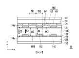
請參照圖1,顯示裝置1包括電控視角切換器11與顯示面板50,其中電控視角切換器11可讓顯示裝置1在分享模式與防窺模式之間進行切換。在本實施例中,顯示面板50例如是液晶顯示面板、或其他合適的非自發光型顯示面板,並選擇性地搭配有背光模組60,電控視角切換器11設置於顯示面板50與背光模組60之間。然而,本發明不限於此,在其他實施例中,顯示裝置1的顯示面板50也可以是有機發光二極體(Organic Light Emitting Diode,OLED)面板、微發光二極體(Micro Light Emitting Diode,Micro LED)面板、或其他合適的自發光型顯示面板,而選擇性地不需背光模組60,且電控視角切換器11係設置在顯示面板50的出光側。Please refer to FIG. 1, the
詳細而言,本實施例的電控視角切換器11包括液晶層110、第一電極121與第二電極122,其中液晶層110包含相對的第一側110a與第二側110b,且第一電極121與第二電極122分別位於液晶層110的第一側110a與第二側110b。詳細而言,當第一電極121與第二電極122被致能而使這兩電極之間具有一電位差,此電位差可在這兩電極之間形成電場以驅使液晶層110的多個液晶分子轉動。換句話說,可透過不同的電場大小與分佈改變多個液晶分子的光軸轉向,以調整電控視角切換器11在不同視角下的出光量(或穿透率),進而將顯示裝置1在分享模式與防窺模式之間進行切換。在本實施例中,第一電極121與第二電極122例如是光穿透式電極,而光穿透式電極的材質包括銦錫氧化物、銦鋅氧化物、鋁錫氧化物、鋁鋅氧化物、或其它合適的氧化物、極薄的金屬、鏤空的金屬層(metal mesh or wire grid)、奈米碳管、奈米銀線(Ag nano-wire)、石墨烯或者是上述至少兩者之堆疊層。In detail, the electrically controlled
進一步而言,電控視角切換器11更包括複數個第一絕緣圖案141與複數個第二絕緣圖案142。在本實施例中,第一絕緣圖案141設置在液晶層110的第一側110a,第二絕緣圖案142設置在液晶層110的第二側110b,且第一絕緣圖案141在方向z上可完全重疊於第二絕緣圖案142。但本發明不以此為限,在其他實施例中,第一絕緣圖案141可至少部分重疊於對應的第二絕緣圖案142。在本實施例中,這些第一絕緣圖案141(或第二絕緣圖案142)可定義出電控視角切換器11的複數個第一透光區TR1與複數個第二透光區TR2,其中相互重疊的第一絕緣圖案141與第二絕緣圖案142的區域定義為第二透光區TR2,而第一透光區TR1位於兩相鄰的第二透光區TR2之間。特別說明的是,為增加第一透光區TR1與第二透光區TR2在穿透率的差異,第一絕緣圖案141及第二絕緣圖案142的厚度總和值較大,因此在本發明中分別設置第一絕緣圖案141與第二絕緣圖案142可避免較大厚度絕緣層製程的困難、避免配向膜或電極層因製程表面斷差的損傷、以及減少絕緣圖案層的垂直面所產生的副作用。Furthermore, the electronically controlled
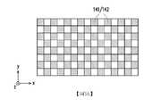
在本實施例中,電控視角切換器11的這些第一絕緣圖案141(或第二絕緣圖案142)各自的外形輪廓例如是正方形,且分別在方向x與方向y上排成多列與多行(如圖3A所示)。更具體地說,這些絕緣圖案(例如第一絕緣圖案141或第二絕緣圖案142)係以棋盤格的樣式排列於基板(例如第一基板101)上。然而,本發明不限於此,在另一實施例中,這些第一絕緣圖案141A(或第二絕緣圖案142A)各自的外形輪廓可以是不同的形狀(例如梯形、三角形、五邊形、或任意的多邊形),且這些第一絕緣圖案141A係以不規則的方式進行排列(如圖3B所示)。在又一實施例中,第一絕緣圖案141B(或第二絕緣圖案142B)也可以是具有字形輪廓的絕緣圖案層(如圖3C所示),或為具有縷空文字的絕緣圖案層。In this embodiment, the contours of the first insulating patterns 141 (or the second insulating patterns 142) of the electronically controlled
從另一觀點來說,在本實施例中,液晶層110可包括在方向x上交替排列的多個第一部分111與多個第二部分112,其中第一部分111與第二部分112分別位於第一透光區TR1與第二透光區TR2。換句話說,液晶層110的第一部分111在方向z上不重疊於第一絕緣圖案141與第二絕緣圖案142,而第二部分112在方向z上重疊於第一絕緣圖案141與第二絕緣圖案142。也因此,液晶層110的第一部分111在方向z上的厚度d1可大於第二部分112在方向z上的厚度d2。亦即,液晶層110的第一部分111所產生的最大相位延遲量(phase retardation)大於第二部分112所產生的最大相位延遲量。在本實施例中,液晶層110的第一部分111的厚度d1可介於1微米至20微米之間,而第二部分112的厚度d2可介於0微米至19微米之間。在一較佳的實施例中,液晶層110的第一部分111的厚度d1與第二部分112的厚度d2之差值可介於0.1微米至19微米之間。From another point of view, in this embodiment, the
特別說明的是,由於第二透光區TR2設有第一絕緣圖案141與第二絕緣圖案142。當第一電極121與第二電極122被致能而具有一特定電壓時,液晶層110的第一部分111與第二部分112受電場影響的程度不同。也就是說,在相同的驅動電壓下,液晶層110的第一部分111所產生的相位延遲量與第二部分112所產生的相位延遲量不同。In particular, the first
另一方面,電控視角切換器11更包括第一基板101、第二基板102、第一配向膜131與第二配向膜132,其中第一配向膜131與第二配向膜132設置在第一基板101與第二基板102之間,且液晶層110夾設於第一配向膜131與第二配向膜132之間。具體而言,第一配向膜131設置於第一基板101上且位於液晶層110的第一側110a,第一電極121位於第一配向膜131與第一基板101之間,第一絕緣圖案141設置在液晶層110的第一側110a且位於第一配向膜131與第一電極121之間;第二配向膜132設置於第二基板102且位於液晶層110的第二側110b,第二電極122位於第二配向膜132與第二基板102之間,第二絕緣圖案142設置在液晶層110的第二側110b且位於第二配向膜132與第二電極122之間。特別說明的是,配向膜係用以排列液晶層110的多個液晶分子(未繪示)使其光軸n定向於預設的方向,而第一基板101與第二基板102例如是透明玻璃基板或是透明軟性基板,其材質例如是玻璃、石英或有機聚合物等。在本實施例中,液晶層110的多個液晶分子是正型液晶分子,且第一配向膜131與第二配向膜132為水平配向膜,但本發明不以此為限。On the other hand, the electronically controlled
特別說明的是,由於第二透光區TR2設有第一絕緣圖案141與第二絕緣圖案142,第一配向膜131與第二配向膜132在第一透光區TR1的間距大於第一配向膜131與第二配向膜132在第二透光區TR2的間距。當第一電極121與第二電極122被致能而具有一特定電壓時,液晶層110的第一部分111相較於第二部分112,更容易被形成的電場所驅動。也就是說,在相同的驅動電壓下,液晶層110的第一部分111所產生的相位延遲量大於第二部分112所產生的相位延遲量,如此有助於加大液晶層110的第一部分111與第二部分112所產生的相位延遲量之差值。In particular, since the second light-transmitting region TR2 is provided with the first
進一步而言,電控視角切換器11更包括第一偏光片151與第二偏光片152,分別設置在液晶層110的第一側110a與第二側110b。更具體地說,第一偏光片151位於第一基板101遠離液晶層110的一側,第二偏光片152位於第二基板102遠離液晶層110的一側。舉例來說,第一偏光片151的吸收軸AX1軸向可平行於第二偏光片152的吸收軸AX2軸向,且液晶層110的光軸n軸向大致上可垂直於兩偏光片的吸收軸。然而,本發明不限於此,根據其他實施例,液晶層110的光軸n軸向與偏光片的吸收軸軸向之間的夾角可介於70度至110度的範圍內。在又一實施例中,液晶層110的光軸n軸向大致上可平行於兩偏光片的吸收軸或夾角可介於-20度至20度的範圍內。特別說明的是,此處垂直於液晶層110的光軸n軸向的方向(即方向x)可定義為電控視角切換器11的視角控制方向(即在方向x上,可控制在不同視角下的出光量或穿透率),且以下說明中的視角(例如圖2所示的視角範圍)皆定義在此視角控制方向上。Furthermore, the electronically controlled
值得一提的是,當顯示裝置1的防窺模式開啟時(即電控視角切換器11被致能)時,由於液晶層110的光軸n軸向大致上垂直於兩偏光片的吸收軸軸向,液晶層110的第一部分111與第二部分112對於來自背光模組60並垂直入射第二基板102的光束而言,並不會產生實質的相位延遲量,意即不改變光束的偏振方向。因此,來自第二偏光片152的光束在通過液晶層110後,可保有其初始的偏振態並通過第一偏光片151。也就是說,在正視角(即視角0度)下,設有第一部分111的第一透光區TR1的穿透率(transmittance)與設有第二部分112的第二透光區TR2的穿透率實質上相等,且這兩透光區於正視角的穿透率為視角範圍內的最大穿透率,如圖2所示。舉例而言,由於第一透光區TR1與第二透光區TR2在正視角下具有實質上相同的最大穿透率,來自背光模組60的光束在通過電控視角切換器11後並未形成干擾影像(例如棋盤格)。因此,顯示面板50的影像畫面(例如統計報表或機密資料)可正常顯示於正視的使用者,如圖4A所示。It is worth mentioning that when the anti-peep mode of the
另一方面,液晶層110的第一部分111與第二部分112對於非垂直入射第二基板102的光束而言,則會產生實質的相位延遲量,意即改變光束的偏振方向,且第一部分111所產生的相位延遲量大於第二部分112所產生的相位延遲量。也就是說,在側視角下,設有第一部份111的第一透光區TR1之穿透率不等於設有第二部分112的第二透光區TR2之穿透率,如圖2所示。舉例來說,在視角43度下,第二透光區TR2的穿透率明顯大於第一透光區TR1的穿透率,且第一透光區TR1於視角43度的穿透率為視角範圍±60度內的最小穿透率。若以43度的視角觀看顯示裝置1,第一透光區TR1因具有最小的穿透率而成為暗區,第二透光區TR2因具有相對較大的穿透率而成為亮區。也就是說,電控視角切換器11在視角43度下可呈現出棋盤格樣式的干擾影像,且此干擾影像與顯示面板50的影像畫面相重疊,如圖4B所示。據此,可有效降低顯示面板50的影像畫面在側視角下的可讀性,進而達到防窺的效果。On the other hand, the
承接上述,相似地,在視角58度下,第一透光區TR1的穿透率明顯大於第二透光區TR2的穿透率,且第二透光區TR2於視角58度的穿透率為視角範圍±60度內的最小穿透率。若以58度的視角觀看顯示裝置1,第二透光區TR2因具有最小的穿透率而成為暗區,第一透光區TR1因具有相對較大的穿透率而成為亮區。也就是說,電控視角切換器11在視角58度下所呈現出的干擾影像(例如棋盤格),其亮暗區的分佈與視角43度下所呈現的干擾影像相反。因此,仍可有效降低顯示面板50的影像畫面在大視角下的可讀性,進而達到防窺的效果。Continuing the above, similarly, at a viewing angle of 58 degrees, the transmittance of the first light transmission area TR1 is significantly greater than that of the second light transmission area TR2, and the transmittance of the second light transmission area TR2 at a viewing angle of 58 degrees It is the minimum penetration rate within the viewing angle range of ±60 degrees. If the
需說明的是,圖4B所示的第一透光區TR1與第二透光區TR2的數量與分佈密度僅作示例性地說明之用,本發明並不以圖式揭示內容為限制。在其他實施例中,第一透光區TR1與第二透光區TR2的數量與分佈密度也可根據實際的防窺需求而調整。It should be noted that the number and distribution density of the first light-transmitting regions TR1 and the second light-transmitting regions TR2 shown in FIG. 4B are for illustrative purposes only, and the present invention is not limited by the content of the drawings. In other embodiments, the number and distribution density of the first light-transmitting area TR1 and the second light-transmitting area TR2 can also be adjusted according to actual privacy requirements.
以下將列舉另一些實施例的電控視角切換器以詳細說明本揭露,其中相同的構件將標示相同的符號,並且省略相同技術內容的說明,省略部分請參考前述實施例,以下不再贅述。特別說明的是,以下實施例的電控視角切換器也可應用於上述實施例的顯示裝置1中。Other embodiments of the electronically controlled viewing angle switcher will be listed below to describe the disclosure in detail. The same components will be marked with the same symbols, and the description of the same technical content will be omitted. For the omitted parts, please refer to the foregoing embodiments, and will not be repeated hereafter. In particular, the electronically controlled viewing angle switch of the following embodiment can also be applied to the
圖5是本發明的第二實施例的電控視角切換器的剖面示意圖。請參照圖5,本實施例的電控視角切換器12與圖1的電控視角切換器11的差異在於:電控視角切換器12更包括複數個第三絕緣圖案143與複數個第四絕緣圖案144,且第三絕緣圖案143在方向z上完全重疊於第四絕緣圖案144。第三絕緣圖案143設置在液晶層110的第一側110a且位於第一配向膜131與第一電極121之間,第四絕緣圖案144設置在液晶層110的第二側110b且位於第二配向膜132與第二電極122之間。第一絕緣圖案141C及第二絕緣圖案142C相似於第一絕緣圖案141及第二絕緣圖案142,差異在於厚度不同。在本實施例中,第一絕緣圖案141C、第二絕緣圖案142C、第三絕緣圖案143與第四絕緣圖案144在方向z上分別具有厚度H1、厚度H2、厚度H3與厚度H4,且第一絕緣圖案141C的厚度H1可大於第三絕緣圖案143的厚度H3,第二絕緣圖案142C的厚度H2可大於第四絕緣圖案144的厚度H4,但本發明不以此為限。在另一實施例中,電控視角切換器12亦可不包含第四絕緣圖案144。5 is a schematic cross-sectional view of the electronically controlled viewing angle switch of the second embodiment of the present invention. 5, the difference between the electronically controlled
另一方面,多個第一絕緣圖案141C與多個第三絕緣圖案143在方向x上交替排列於液晶層110A的第一側110a,多個第二絕緣圖案142C與第四絕緣圖案144在方向x上交替排列於液晶層110A的第二側110b。舉例來說,第一絕緣圖案141C與第三絕緣圖案143可為同一膜層,第二絕緣圖案142C與第四絕緣圖案144可為同一膜層;也就是說,第一絕緣圖案141C與第三絕緣圖案143(或者是第二絕緣圖案142C與第四絕緣圖案144)可定義出一絕緣層的凹凸結構,但本發明不以此為限。On the other hand, the plurality of
進一步而言,第三絕緣圖案143(或第四絕緣圖案144)與第一絕緣圖案141C(或第二絕緣圖案142C)可分別定義出電控視角切換器12的第一透光區TR1與第二透光區TR2。在本實施例中,液晶層110A位於第一透光區TR1的第一部分111在方向z上具有厚度d3,液晶層110A位於第二透光區TR2的第二部分112在方向z上具有厚度d4,且第一部分111的厚度d3大於第二部分112的厚度d4。換句話說,液晶層110A的第一部分111所產生的最大相位延遲量(phase retardation)可大於第二部分112所產生的最大相位延遲量。據此,在側視角下,電控視角切換器12的第一透光區TR1的出光量(或穿透率)可顯著地不同於第二透光區TR2的出光量(或穿透率),以形成圖案化的干擾影像。Furthermore, the third insulating pattern 143 (or the fourth insulating pattern 144) and the first
圖6是本發明的第三實施例的電控視角切換器的剖面示意圖。請參照圖6,本實施例的電控視角切換器13與圖1的電控視角切換器11的主要差異在於:第一絕緣圖案141與第二絕緣圖案142的相對配置關係以及相應產生的液晶層110的厚度差異。在本實施例中,第一絕緣圖案141在方向z上可部分重疊於第二絕緣圖案142(亦即,第一絕緣圖案141可錯位於第二絕緣圖案142)。第一絕緣圖案141與第二絕緣圖案142可定義出電控視角切換器13的第一透光區TR1、第二透光區TR2與第三透光區TR3,且第三透光區TR3位於第一透光區TR1與第二透光區TR2之間。6 is a schematic cross-sectional view of the electronically controlled viewing angle switch of the third embodiment of the present invention. Please refer to FIG. 6, the main difference between the electronically controlled
進一步而言,液晶層110B位於第一透光區TR1的第一部分111A在方向z上具有厚度d1,液晶層110B位於第二透光區TR2的第二部分112A在方向z上具有厚度d2,液晶層110B位於第三透光區TR3的第三部分113在方向z上具有厚度d5,且第一部分111A的厚度d1大於第三部分的113的厚度d5,第二部分112A的厚度d2小於第三部分113的厚度d5。換句話說,液晶層110B的第一部分111A所產生的最大相位延遲量(phase retardation)大於第三部分113所產生的最大相位延遲量,而第二部分112A所產生的最大相位延遲量小於第三部分113所產生的最大相位延遲量。據此,在側視角下,電控視角切換器13的第一透光區TR1、第二透光區TR2與第三透光區TR3各自的穿透率(或出光量)可顯著地不同於彼此,以形成圖案化的干擾影像。Furthermore, the
圖7是本發明的第四實施例的電控視角切換器的剖面示意圖。請參照圖7,本實施例的電控視角切換器14與圖6的電控視角切換器13的主要差異在於:第一絕緣圖案與第二絕緣圖案的厚度不同。在本實施例中,第一絕緣圖案141與第二絕緣圖案142C分別具有厚度H5與厚度H6,且第二絕緣圖案142C的厚度H6可選擇性地大於第一絕緣圖案141的厚度H5,但本發明不以此為限。第一絕緣圖案141與第二絕緣圖案142C可定義出電控視角切換器14的第一透光區TR1、第二透光區TR2、第三透光區TR3與第四透光區TR4,且第三透光區TR3位於第一透光區TR1與第二透光區TR2之間,第二透光區TR2位於第三透光區TR3與第四透光區TR4之間。FIG. 7 is a schematic cross-sectional view of the electronically controlled viewing angle switch of the fourth embodiment of the present invention. Please refer to FIG. 7, the main difference between the electronically controlled
進一步而言,液晶層110C位於第一透光區TR1的第一部分111A在方向z上具有厚度d1,液晶層110C位於第二透光區TR2的第二部分112B在方向z上具有厚度d6,液晶層110C位於第三透光區TR3的第三部分113在方向z上具有厚度d5,液晶層110C位於第四透光區TR4的第四部分114在方向z上具有厚度d7,且第一部分111A的厚度d1大於第三部分113的厚度d5,第三部分113的厚度d5大於第四部分114的厚度d7,第二部分112A的厚度d6小於第四部分114的厚度d7。換句話說,液晶層110C的第一部分111A所產生的最大相位延遲量(phase retardation)大於第三部分113所產生的最大相位延遲量,液晶層110C的第三部分113所產生的最大相位延遲量大於第四部分114所產生的最大相位延遲量,而第二部分112B所產生的最大相位延遲量小於第四部分114所產生的最大相位延遲量。據此,在側視角下,電控視角切換器14的第一透光區TR1、第二透光區TR2、第三透光區TR3與第四透光區TR4各自的穿透率(或出光量)可顯著地不同於彼此,以形成圖案化的干擾影像。Furthermore, the
圖8是本發明的第五實施例的電控視角切換器的剖面示意圖。請參照圖8,本實施例的電控視角切換器15與圖1的電控視角切換器11的主要差異在於:電控視角切換器15更包括複數個第三絕緣圖案143A與複數個第四絕緣圖案144A,且第三絕緣圖案143A與第四絕緣圖案144A的介電常數不同於第一絕緣圖案141與第二絕緣圖案142的介電常數。在另一實施例中,電控視角切換器15亦可不包含第四絕緣圖案144A。FIG. 8 is a schematic cross-sectional view of the electronically controlled viewing angle switch of the fifth embodiment of the present invention. Referring to FIG. 8, the main difference between the electronically controlled
舉例而言,第一絕緣圖案141的介電常數可大於第三絕緣圖案143A的介電常數,第二絕緣圖案142的介電常數可大於第四絕緣圖案144A的介電常數。第一絕緣圖案141與第二絕緣圖案142的介電常數可介於3至80的範圍內。亦即,第一絕緣圖案141與第二絕緣圖案142的材質可以是較高介電常數的材料。在本實施例中,第一絕緣圖案141與第二絕緣圖案142的材料可包括氮化矽(Si3N4)、氧化鋁(Al2O3)、氧化釔(Y2O3)、二氧化鈦(TiO2)、二氧化鉿(HfO2)、二氧化鋯(ZrO2)、或其他適合的高介電常數材料。在本實施例中,第一絕緣圖案141的厚度H7可等於第三絕緣圖案143A的厚度H9,第二絕緣圖案142的厚度H8可等於第四絕緣圖案144A的厚度H10,但本發明不以此為限。根據其他實施例,第一絕緣圖案的厚度也可大於第三絕緣圖案的厚度,第二絕緣圖案的厚度也可大於第四絕緣圖案的厚度。For example, the dielectric constant of the first
另一方面,多個第一絕緣圖案141與多個第三絕緣圖案143A在方向x上交替排列於液晶層110D的第一側110a,多個第二絕緣圖案142與第四絕緣圖案144A在方向x上交替排列於液晶層110D的第二側110b。第三絕緣圖案143A(或第四絕緣圖案144A)與第一絕緣圖案141(或第二絕緣圖案142)可分別定義出電控視角切換器15的第一透光區TR1與第二透光區TR2。在本實施例中,液晶層110D位於第一透光區TR1的第一部分111B在方向z上具有厚度d8,液晶層110D位於第二透光區TR2的第二部分112在方向z上具有厚度d9,且第一部分111B的厚度d8實質上可等於第二部分112的厚度d9。也就是說,液晶層110D僅具有單一厚度。On the other hand, the plurality of
值得一提的是,在本實施例中,當第一電極121與第二電極122被致能而具有一特定電壓時,因為第一透光區TR1及第二透光區TR2中的絕緣圖案具有不同的介電常數,因此相重疊的第一絕緣圖案141與第二絕緣圖案142之間所形成的電場E2強度可小於相重疊的第三絕緣圖案143A與第四絕緣圖案144A之間所形成的電場E1強度。也就是說,當電控視角切換器15被致能時,可於兩電極間形成對應於多個第一絕緣圖案141與多個第三絕緣圖案143A(或者是第二絕緣圖案142與第四絕緣圖案144A)的電場強度分佈。It is worth mentioning that in this embodiment, when the
進一步而言,兩電極在第一透光區TR1與第二透光區TR2所形成的電場強度差異,使得液晶層110D在這兩透光區的第一部分111B與第二部分112的液晶分子被電場轉動的程度不同,造成液晶層110D的第一部分111B所產生的相位延遲量不同於第二部分112所產生的相位延遲量。因此,電控視角切換器15的第一透光區TR1與第二透光區TR2各自的穿透率(或出光量)在側視角下可顯著地不同。舉例來說,第一透光區TR1與第二透光區TR2可分別為暗區與亮區,且電控視角切換器15的多個第一透光區TR1與多個第二透光區TR2可排列出圖案化的干擾影像,以降低顯示面板(如圖1所示)的影像畫面在側視角下的可讀性,進而達到防窺的效果。Furthermore, the difference in the electric field intensity formed by the two electrodes in the first light-transmitting region TR1 and the second light-transmitting region TR2 makes the liquid crystal molecules of the
圖9是本發明的第六實施例的電控視角切換器的剖面示意圖。請參照圖9,本實施例的電控視角切換器16與圖8的電控視角切換器15的差異在於:電控視角切換器16的液晶層110D的第二側110b不設有絕緣圖案(例如圖8的第二絕緣圖案142與第四絕緣圖案144A)。也就是說,電控視角切換器16只在液晶層110D的第一側110a設有絕緣圖案。在本實施例中,第一絕緣圖案141的厚度可等於第三絕緣圖案143A的厚度,當第一電極121與第二電極122被致能時,僅透過設置在液晶層110D一側的第一絕緣圖案141與第三絕緣圖案143A,也可造成兩電極於第一透光區TR1與第二透光區TR2所產生的電場強度的明顯差異。舉例來說,兩電極於第一透光區TR1與第二透光區TR2分別產生電場E1’與電場E2’,且電場E1’的強度可大於電場E2’的強度。換句話說,透過第一絕緣圖案141與第三絕緣圖案143A的介電常數差值的增加,可縮減絕緣圖案層的配置數量,有助於簡化製造流程。9 is a schematic cross-sectional view of the electronically controlled viewing angle switch of the sixth embodiment of the present invention. 9, the difference between the electronically controlled
圖10是本發明的第七實施例的電控視角切換器的剖面示意圖。請參照圖10,本實施例的電控視角切換器17與圖8的電控視角切換器15的主要差異在於:電控視角切換器17不具有如圖8所示的第四絕緣圖案144A,且可選擇性地包括折射率匹配層160。在本實施例中,由於第一透光區TR1不設有如圖8所示的第四絕緣圖案144A,液晶層110E的第一部分111B的厚度d10可大於第二部分112的厚度d9,且第一電極121與第二電極122在第一透光區TR1所形成的電場E3與在第二透光區TR2所形成的電場E2強度差異可進一步擴大。亦即,在本實施例中,可透過在兩電極間形成對應這些絕緣圖案的電場強度分佈以及液晶層110E的厚度分佈,使液晶層110E的第一部分111B於側視角的相位延遲量不同於第二部分112於側視角的相位延遲量。10 is a schematic cross-sectional view of the electronically controlled viewing angle switch of the seventh embodiment of the present invention. 10, the main difference between the electronically controlled
特別說明的是,在本實施例中,第一絕緣圖案141的材質可選擇為高介電常數的材料,因此第一絕緣圖案141的厚度與第二絕緣圖案142的厚度的厚度總和可具有較小的厚度總和值,但仍保持大於第三絕緣圖案143的厚度。例如第二絕緣圖案142的厚度值可以小於5微米或是等於零,使得厚度總和值均由第一絕緣圖案141所貢獻,搭配高介電常數材料的使用,同樣能達到第一透光區TR1與第二透光區TR2各自的穿透率(或出光量)有顯著地不同的功效。In particular, in this embodiment, the material of the first
另一方面,為了多個第一絕緣圖案141與多個第三絕緣圖案143的交界處在正視角下不輕易被觀察到,電控視角切換器17還可包括折射率匹配層160。在本實施例中,折射率匹配層160設置於液晶層110E的第一側110a,且位於第一電極121遠離液晶層110E的一側,但本發明不以此為限。在其他實施例中,折射率匹配層160也可設置在第一基板101與第一偏光片151之間(或者是第二基板102與第二電極122之間)、第一基板101上的絕緣圖案(第一絕緣圖案141、第三絕緣圖案143)與第一電極121之間、或者是第一基板101上的絕緣圖案(第一絕緣圖案141、第三絕緣圖案143)與第一配向膜131之間。舉例而言,折射率匹配層160包括複數個第一匹配部161與複數個第二匹配部162。第一匹配部161與第二匹配部162在方向z上分別重疊於第一絕緣圖案141與第三絕緣圖案143。在另一實施例中,折射率匹配層160也可以是非圖案化設計,且設置於第一絕緣圖案141與第一電極121之間。On the other hand, in order that the boundary between the plurality of
進一步而言,第一絕緣圖案141的折射率大於第三絕緣圖案143的折射率,且第一匹配部161的折射率小於第二匹配部162的折射率。也就是說,透過折射率匹配層160的兩匹配部的折射率差值來補償第一絕緣圖案141與第三絕緣圖案143的折射率差值,可降低絕緣圖案層於正視下的可視性,有助於提升顯示裝置的視覺品味。Furthermore, the refractive index of the first
圖11是本發明的第八實施例的電控視角切換器的剖面示意圖。請參照圖11,本實施例的電控視角切換器18與圖8的電控視角切換器15的主要差異在於:電控視角切換器18的第一基板101上的絕緣圖案與第二基板102上的絕緣圖案之間的相對配置關係。具體而言,第一絕緣圖案141(或第三絕緣圖案143A)在方向z上可部分重疊於第二絕緣圖案142(或第四絕緣圖案144A)。也就是說,第一絕緣圖案141可錯位於第二絕緣圖案142,且第三絕緣圖案143A可錯位於第四絕緣圖案144A。透過此處的錯位關係,可定義出電控視角切換器18的第一透光區TR1、第二透光區TR2與第三透光區TR3,且第三透光區TR3位於第一透光區TR1與第二透光區TR2之間。11 is a schematic cross-sectional view of the electronically controlled viewing angle switch of the eighth embodiment of the present invention. 11, the main difference between the electronically controlled
在本實施例中,當第一電極121與第二電極122被致能時,由於第一絕緣圖案141與第二絕緣圖案142的介電常數大於第三絕緣圖案143A與第四絕緣圖案144A的介電常數,兩電極在第一透光區TR1、第二透光區TR2與第三透光區TR3分別形成不同強度的電場E1、電場E2與電場E4。更具體地說,相重疊的第一絕緣圖案141與第二絕緣圖案142之間所形成的電場E2強度可小於相重疊的第一絕緣圖案141與第四絕緣圖案144A之間所形成的電場E4強度,且相重疊的第三絕緣圖案143A與第四絕緣圖案144A之間所形成的電場E1強度可大於相重疊的第一絕緣圖案141與第四絕緣圖案144A之間所形成的電場E4強度。In this embodiment, when the
進一步而言,兩電極在第一透光區TR1、第二透光區TR2與第三透光區TR3所產生的電場強度差異,使得液晶層110D在這些透光區的第一部分111C、第二部分112C與第三部分113A的液晶分子被電場轉動的程度不同,造成液晶層110D的第一部分111C、第二部分112C與第三部分113A各自於側視角所產生的相位延遲量都不同。因此,電控視角切換器18的第一透光區TR1、第二透光區TR2與第三透光區TR3各自的穿透率(或出光量)在側視角下可顯著地不同。舉例來說,第一透光區TR1、第二透光區TR2與第三透光區TR3可分別為暗區、亮區與微亮區,且電控視角切換器18的多個第一透光區TR1、多個第二透光區TR2與多個第三透光區TR3可排列出圖案化的干擾影像,以降低顯示面板(如圖1所示)的影像畫面在側視角下的可讀性,進而達到防窺的效果。Furthermore, the difference in the electric field intensity generated by the two electrodes in the first light-transmitting area TR1, the second light-transmitting area TR2 and the third light-transmitting area TR3 makes the
值得一提的是,由於第一絕緣圖案141與第三絕緣圖案143A分別錯位於第二絕緣圖案142與第四絕緣圖案144A。在正視角下,透過第二絕緣圖案142與第四絕緣圖案144A的折射率差值,可部分地補償第一絕緣圖案141與第三絕緣圖案143A的折射率差值,以降低絕緣圖案層於正視下的可視性,有助於提升顯示裝置在操作時的視覺品味。It is worth mentioning that the
圖12是本發明的第九實施例的電控視角切換器的剖面示意圖。請參照圖12,本實施例的電控視角切換器19與圖1的電控視角切換器11的主要差異在於:絕緣圖案的配置關係。在本實施例中,第一配向膜131A與第二配向膜132A分別設置於液晶層110F的第一側110a與第二側110b,第一絕緣圖案141D與第二絕緣圖案142D設置在第一配向膜131A與第二配向膜132A之間,且第一絕緣圖案141D位於第一配向膜131A與液晶層110F之間,且第二絕緣圖案142D位於第二配向膜132A與液晶層110F之間,並且選擇性地第一絕緣圖案141D連接第二絕緣圖案142D。也就是說,液晶層110F的多個液晶分子LC大致上都分布在兩相鄰的第一絕緣圖案141D(或第二絕緣圖案142D)之間(即第一透光區TR1)。但本發明不以此為限,在其他實施例中,第一絕緣圖案141D與第一配向膜131A可間隔排列(或第二絕緣圖案142D與第二配向膜132A可間隔排列),亦即第一絕緣圖案141D設置於第一電極121上,而第一配向膜131A位於第一絕緣圖案141D外的區域,亦即第一配向膜131A僅設置於對應於第一透光區TR1的第一電極121上。12 is a schematic cross-sectional view of the electronically controlled viewing angle switch of the ninth embodiment of the present invention. Please refer to FIG. 12, the main difference between the electronically controlled
由於第二透光區TR2大致上被第一絕緣圖案141D與第二絕緣圖案142D所佔據,入射此區的光束無論是以何種角度入射都可保有其初始的偏振態並通過第一偏光片151。也就是說,無論電控視角切換器19是否被致能,本實施例的第二透光區TR2都恆為亮區。當第一電極121與第二電極122被致能時,液晶層110F的第一部分111D於側視角下所產生的相位延遲量,可讓第一透光區TR1成為暗區。藉此,以形成圖案化的干擾影像。在本實施例中,液晶層110F可包括多個負型液晶分子LC,且第一配向膜131A與第二配向膜132A為垂直配向膜,但本發明不以此為限。特別說明的是,此處的垂直配向膜係用以排列多個負型液晶分子LC,使液晶層110F的光軸與基板的法線方向(即方向z)夾一小於20度的角度。Since the second light-transmitting area TR2 is roughly occupied by the first insulating
圖13是本發明的第十實施例的電控視角切換器的剖面示意圖。請參照圖13,本實施例的電控視角切換器20與圖1的電控視角切換器11的差異在於:電極的配置關係。具體而言,電控視角切換器20的第一電極121A係設置在第一絕緣圖案141與液晶層110之間,且第二電極122A係設置在第二絕緣圖案142與液晶層110之間。13 is a schematic cross-sectional view of the electronically controlled viewing angle switch of the tenth embodiment of the present invention. Please refer to FIG. 13, the difference between the electronically controlled
透過此配置關係,第一電極121A與第二電極122A在第二透光區TR2的間距可小於第一電極121A與第二電極122A在第一透光區TR1的間距。當兩電極被致能時,液晶層110的第二部分112所感受到的電場強度可大於第一部分111所感受到的電場強度。也就是說,在本實施例中,可透過在兩電極間形成對應這些絕緣圖案的電場強度分佈以及液晶層110的厚度分佈,使液晶層110的第一部分111於側視角的相位延遲量不同於第二部分112於側視角的相位延遲量。Through this configuration relationship, the distance between the
圖14是本發明的第十一實施例的電控視角切換器的剖面示意圖。請參照圖14,本實施例的電控視角切換器21與圖1的電控視角切換器11的主要差異在於:電控視角切換器更包含一相位延遲膜。更具體地說,電控視角切換器21更包括位於第一偏光片151與第二偏光片152之間的相位延遲膜170。在本實施例中,相位延遲膜170可選擇性地設置於第一偏光片151與第一基板101之間,但本發明不以此為限。在另一實施例中,相位延遲膜170也可設置在第二偏光片152與第二基板102之間。在又一實施例中,相位延遲膜170也可設置在第一基板101與液晶層110之間,或第二基板102與液晶層110之間。14 is a schematic cross-sectional view of the electronically controlled viewing angle switch of the eleventh embodiment of the present invention. Please refer to FIG. 14, the main difference between the electronically controlled
進一步而言,相位延遲膜170可包括複數個第一部分171與複數個第二部分172,且這些第一部分171與這些第二部分172沿方向x交替排列於第一基板101上。亦即,相位延遲膜170可以是圖案化的相位延遲膜,相位延遲膜170的第一部分171在方向z上可完全重疊於第一絕緣圖案141,而第二部分172位於兩相鄰的第一部分171之間。也就是說,相位延遲膜170的第一部分171與第二部分172分別位於第二透光區TR2與第一透光區TR1。當電控視角切換器21操作在防窺模式時(即兩電極被致能時),相位延遲膜170的配置可加大兩透光區在離軸(off-axis)視角下的相位延遲差異。本發明不限於此,在其他實施例中,相位延遲膜170可設計為當電控視角切換器21操作在分享模式時(即兩電極不被致能時),透過圖案化之相位延遲膜170的配置,可補償第一透光區TR1與第二透光區TR2在側視角下的穿透率差值,進而提升顯示裝置在側視角下的顯示品質。Furthermore, the
在本實施例中,相位延遲膜170的第一部分171與第二部分172的厚度方向相位延遲值(即Rth)之差值可介於50nm至1000nm之間。在一較佳的實施例中,相位延遲膜170的第一部分171與第二部分172的厚度方向相位延遲值(即Rth)之差值可介於200nm至400nm之間。然而,本發明不限於此,根據其他實施例,電控視角切換器的相位延遲膜也可以是非圖案化的相位延遲膜,且其厚度方向相位延遲值可介於250nm至600nm之間。需說明的是,此處的厚度方向相位延遲值(即Rth)係為相位延遲膜170在可見光的波長範圍內所產生的相位延遲值。In this embodiment, the difference between the thickness direction retardation value (ie Rth) of the
本實施例的相位延遲膜數量係以一個為例進行示範性地說明,並非以此而加以限制本發明。在另一實施例中,電控視角切換器也可包括兩個B型板(Bi-Axial plate),其中一B型板位於第一偏光片151與液晶層110之間,或第一偏光片151與第一基板101之間,而另一B型板則位於第二偏光片152與第二基板102之間。在本實施例中,相位延遲膜170例如是C型板(C-plate)、負C型板(negative C-plate)、A型板(A-plate)、B型板(Bi-Axial plate)、O型板(O-plate)、或者是光軸彼此相交的兩A型板(A-plate)所構成的複合板,但本發明不以此為限。The number of phase retardation films in this embodiment is illustrated by taking one as an example, and the present invention is not limited by this. In another embodiment, the electronically controlled viewing angle switch may also include two Bi-Axial plates, one of which is located between the
綜上所述,在本發明之一實施例的電控視角切換器與顯示裝置中,透過多個絕緣圖案設置在液晶層的至少一側,可在兩電極間形成對應這些絕緣圖案的電場強度分佈或液晶層的厚度分佈,以使液晶層的至少兩部分具有不同的相位延遲值。據此,電控視角切換器可具有對應於這些絕緣圖案的多個透光區,且這些透光區在側視角下的穿透率差異較大以形成圖案化的干擾影像,有助於提升顯示裝置的防窺性能。In summary, in the electrically controlled viewing angle switch and display device of an embodiment of the present invention, through a plurality of insulating patterns disposed on at least one side of the liquid crystal layer, an electric field intensity corresponding to these insulating patterns can be formed between the two electrodes. Distribution or thickness distribution of the liquid crystal layer so that at least two parts of the liquid crystal layer have different phase retardation values. Accordingly, the electronically controlled viewing angle switch can have multiple light-transmitting regions corresponding to these insulating patterns, and the transmissivity of these light-transmitting regions under side viewing angles has a large difference to form a patterned interference image, which helps to improve The privacy performance of the display device.
雖然本發明已以實施例揭露如上,然其並非用以限定本發明,任何所屬技術領域中具有通常知識者,在不脫離本發明的精神和範圍內,當可作些許的更動與潤飾,故本發明的保護範圍當視後附的申請專利範圍所界定者為準。Although the present invention has been disclosed in the above embodiments, it is not intended to limit the present invention. Anyone with ordinary knowledge in the technical field can make some changes and modifications without departing from the spirit and scope of the present invention. The scope of protection of the present invention shall be determined by the scope of the attached patent application.
1:顯示裝置 11 ~ 21:電控視角切換器 50:顯示面板 60:背光模組 101:第一基板 102:第二基板 110、110A、110B、110C、110D、110E、110F:液晶層 110a:第一側 110b:第二側 111、111A、111B、111C、111D:第一部分 112、112A、112B、112C:第二部分 113、113A:第三部分 114:第四部分 121、121A:第一電極 122、122A:第二電極 131、131A:第一配向膜 132、132A:第二配向膜 141、141A、141B、141C、141D:第一絕緣圖案 142、142A、142B、142C、142D:第二絕緣圖案 143、143A:第三絕緣圖案 144、144A:第四絕緣圖案 151:第一偏光片 152:第二偏光片 160:折射率匹配層 161:第一匹配部 162:第二匹配部 170:相位延遲膜 171:第一部分 172:第二部分 AX1、AX2:吸收軸 d1 ~ d10、H1 ~ H10:厚度 E1、E2、E1’、E2’、E3、E4:電場 n:光軸 TR1、TR2、TR3、TR4:透光區 x、y、z:方向1:
圖1是本發明的第一實施例的顯示裝置的剖面示意圖。 圖2是圖1的電控視角切換器的視角對穿透率的曲線圖。 圖3A是圖1的絕緣圖案的俯視示意圖。 圖3B及圖3C是本發明的另一些實施例的絕緣圖案的俯視示意圖。 圖4A及圖4B是圖1的顯示裝置於不同視角下的顯示效果的示意圖。 圖5是本發明的第二實施例的電控視角切換器的剖面示意圖。 圖6是本發明的第三實施例的電控視角切換器的剖面示意圖。 圖7是本發明的第四實施例的電控視角切換器的剖面示意圖。 圖8是本發明的第五實施例的電控視角切換器的剖面示意圖。 圖9是本發明的第六實施例的電控視角切換器的剖面示意圖。 圖10是本發明的第七實施例的電控視角切換器的剖面示意圖。 圖11是本發明的第八實施例的電控視角切換器的剖面示意圖。 圖12是本發明的第九實施例的電控視角切換器的剖面示意圖。 圖13是本發明的第十實施例的電控視角切換器的剖面示意圖。 圖14是本發明的第十一實施例的電控視角切換器的剖面示意圖。FIG. 1 is a schematic cross-sectional view of a display device according to a first embodiment of the invention. FIG. 2 is a graph of the viewing angle vs. penetration rate of the electronically controlled viewing angle switch of FIG. 1. 3A is a schematic top view of the insulation pattern of FIG. 1. 3B and 3C are schematic top views of insulating patterns of other embodiments of the present invention. 4A and 4B are schematic diagrams of display effects of the display device in FIG. 1 under different viewing angles. 5 is a schematic cross-sectional view of the electronically controlled viewing angle switch of the second embodiment of the present invention. 6 is a schematic cross-sectional view of the electronically controlled viewing angle switch of the third embodiment of the present invention. FIG. 7 is a schematic cross-sectional view of the electronically controlled viewing angle switch of the fourth embodiment of the present invention. FIG. 8 is a schematic cross-sectional view of the electronically controlled viewing angle switch of the fifth embodiment of the present invention. 9 is a schematic cross-sectional view of the electronically controlled viewing angle switch of the sixth embodiment of the present invention. 10 is a schematic cross-sectional view of the electronically controlled viewing angle switch of the seventh embodiment of the present invention. 11 is a schematic cross-sectional view of the electronically controlled viewing angle switch of the eighth embodiment of the present invention. 12 is a schematic cross-sectional view of the electronically controlled viewing angle switch of the ninth embodiment of the present invention. 13 is a schematic cross-sectional view of the electronically controlled viewing angle switch of the tenth embodiment of the present invention. 14 is a schematic cross-sectional view of the electronically controlled viewing angle switch of the eleventh embodiment of the present invention.
1:顯示裝置1: display device
11:電控視角切換器11: Electronically controlled viewing angle switch
50:顯示面板50: display panel
60:背光模組60: Backlight module
101:第一基板101: first substrate
102:第二基板102: second substrate
110:液晶層110: liquid crystal layer
110a:第一側110a: first side
110b:第二側110b: second side
111:第一部分111: Part One
112:第二部分112: Part Two
121:第一電極121: first electrode
122:第二電極122: second electrode
131:第一配向膜131: first alignment film
132:第二配向膜132: Second alignment film
141:第一絕緣圖案141: first insulation pattern
142:第二絕緣圖案142: second insulation pattern
151:第一偏光片151: The first polarizer
152:第二偏光片152: second polarizer
AX1、AX2:吸收軸AX1, AX2: Absorption axis
d1、d2:厚度d1, d2: thickness
n:光軸n: optical axis
TR1、TR2:透光區TR1, TR2: light transmission area
x、z:方向x, z: direction
Claims (16)
Translated fromChineseApplications Claiming Priority (2)
| Application Number | Priority Date | Filing Date | Title |
|---|---|---|---|
| CN201910748129.3ACN112394558B (en) | 2019-08-14 | 2019-08-14 | Electric control visual angle switcher and display device |
| CN201910748129.3 | 2019-08-14 |
Publications (2)
| Publication Number | Publication Date |
|---|---|
| TWI709798Btrue TWI709798B (en) | 2020-11-11 |
| TW202107179A TW202107179A (en) | 2021-02-16 |
Family
ID=74202117
Family Applications (1)
| Application Number | Title | Priority Date | Filing Date |
|---|---|---|---|
| TW108130005ATWI709798B (en) | 2019-08-14 | 2019-08-22 | Electrically controllable viewing angle switch device and display apparatus |
Country Status (3)
| Country | Link |
|---|---|
| US (1) | US11709385B2 (en) |
| CN (1) | CN112394558B (en) |
| TW (1) | TWI709798B (en) |
Cited By (1)
| Publication number | Priority date | Publication date | Assignee | Title |
|---|---|---|---|---|
| TWI884736B (en)* | 2024-01-22 | 2025-05-21 | 中強光電股份有限公司 | Anti-peep module and display apparatus |
Families Citing this family (4)
| Publication number | Priority date | Publication date | Assignee | Title |
|---|---|---|---|---|
| JP7225424B2 (en)* | 2019-09-27 | 2023-02-20 | 富士フイルム株式会社 | optical element |
| TWI834290B (en)* | 2021-10-26 | 2024-03-01 | 群創光電股份有限公司 | Electronic device |
| CN116940152A (en)* | 2022-03-31 | 2023-10-24 | 群创光电股份有限公司 | electronic device |
| CN221175190U (en)* | 2023-09-22 | 2024-06-18 | 中强光电股份有限公司 | Electric control panel and display device |
Citations (5)
| Publication number | Priority date | Publication date | Assignee | Title |
|---|---|---|---|---|
| TW466365B (en)* | 1997-12-25 | 2001-12-01 | Sharp Kk | Liquid crystal display device |
| TW201232122A (en)* | 2011-01-31 | 2012-08-01 | Univ Nat Chiao Tung | Backlight device with angle adjustment |
| TWI494607B (en)* | 2012-12-27 | 2015-08-01 | Toppan Printing Co Ltd | Liquid crystal display device, substrate for liquid crystal display device, and method for manufacturing substrate for liquid crystal display device |
| TWI597551B (en)* | 2017-03-03 | 2017-09-01 | 友達光電股份有限公司 | Display device |
| CN207650518U (en)* | 2017-12-26 | 2018-07-24 | 扬升照明股份有限公司 | Viewing angle switchable device and viewing angle switchable display module |
Family Cites Families (16)
| Publication number | Priority date | Publication date | Assignee | Title |
|---|---|---|---|---|
| DE3400438A1 (en)* | 1984-01-09 | 1985-07-18 | Vdo Adolf Schindling Ag, 6000 Frankfurt | DISPLAY DEVICE |
| TWI266939B (en)* | 2003-09-29 | 2006-11-21 | Sharp Kk | Liquid crystal display apparatus |
| JP4390595B2 (en)* | 2004-03-09 | 2009-12-24 | シャープ株式会社 | Liquid crystal display |
| JP5095941B2 (en) | 2005-12-28 | 2012-12-12 | エルジー ディスプレイ カンパニー リミテッド | Liquid crystal display |
| TWI348064B (en)* | 2006-05-19 | 2011-09-01 | Au Optronics Corp | Pixel structure and liquid crystal display panel |
| KR101291716B1 (en)* | 2009-12-11 | 2013-07-31 | 엘지디스플레이 주식회사 | Liquid crystal display device for liquid crystal modes requiring high drive voltag |
| CN101738808B (en)* | 2010-01-08 | 2011-08-31 | 友达光电股份有限公司 | Display panel, alignment method and operation method thereof, and color filter substrate |
| TW201423206A (en)* | 2012-12-14 | 2014-06-16 | Au Optronics Corp | Liquid crystal display panel |
| TWM500302U (en)* | 2014-08-18 | 2015-05-01 | Unidisplay Inc | Touch panel and touch display device |
| CN104155814A (en)* | 2014-08-29 | 2014-11-19 | 昆山龙腾光电有限公司 | Liquid crystal display device and manufacturing method thereof |
| TWI596402B (en)* | 2016-08-17 | 2017-08-21 | 友達光電股份有限公司 | Liquid crystal display panel |
| US20210181551A1 (en)* | 2016-10-04 | 2021-06-17 | Jsr Corporation | Liquid crystal device and method of manufacture therefor |
| CN108345139B (en)* | 2017-01-25 | 2022-04-22 | 中强光电股份有限公司 | Viewing angle switchable display device |
| CN207249281U (en)* | 2017-09-25 | 2018-04-17 | 昆山龙腾光电有限公司 | The changeable liquid crystal display device in visual angle |
| CN108897151B (en) | 2018-07-17 | 2021-06-22 | 昆山龙腾光电股份有限公司 | Liquid crystal display device with switchable viewing angle |
| CN109324449B (en)* | 2018-11-15 | 2021-06-22 | 昆山龙腾光电股份有限公司 | Liquid crystal display device and driving method thereof |
- 2019
- 2019-08-14CNCN201910748129.3Apatent/CN112394558B/enactiveActive
- 2019-08-22TWTW108130005Apatent/TWI709798B/enactive
- 2020
- 2020-07-28USUS16/940,401patent/US11709385B2/enactiveActive
Patent Citations (5)
| Publication number | Priority date | Publication date | Assignee | Title |
|---|---|---|---|---|
| TW466365B (en)* | 1997-12-25 | 2001-12-01 | Sharp Kk | Liquid crystal display device |
| TW201232122A (en)* | 2011-01-31 | 2012-08-01 | Univ Nat Chiao Tung | Backlight device with angle adjustment |
| TWI494607B (en)* | 2012-12-27 | 2015-08-01 | Toppan Printing Co Ltd | Liquid crystal display device, substrate for liquid crystal display device, and method for manufacturing substrate for liquid crystal display device |
| TWI597551B (en)* | 2017-03-03 | 2017-09-01 | 友達光電股份有限公司 | Display device |
| CN207650518U (en)* | 2017-12-26 | 2018-07-24 | 扬升照明股份有限公司 | Viewing angle switchable device and viewing angle switchable display module |
Cited By (1)
| Publication number | Priority date | Publication date | Assignee | Title |
|---|---|---|---|---|
| TWI884736B (en)* | 2024-01-22 | 2025-05-21 | 中強光電股份有限公司 | Anti-peep module and display apparatus |
Also Published As
| Publication number | Publication date |
|---|---|
| US11709385B2 (en) | 2023-07-25 |
| CN112394558A (en) | 2021-02-23 |
| US20210048696A1 (en) | 2021-02-18 |
| CN112394558B (en) | 2023-08-08 |
| TW202107179A (en) | 2021-02-16 |
Similar Documents
| Publication | Publication Date | Title |
|---|---|---|
| TWI709798B (en) | Electrically controllable viewing angle switch device and display apparatus | |
| CN100445810C (en) | Display device, viewing angle control device, and electronic device | |
| JP3823972B2 (en) | Viewing angle control element, display device, and electronic device | |
| TW451097B (en) | Liquid crystal device and electronic device | |
| JP4531035B2 (en) | Liquid crystal display device and driving method thereof | |
| JP4494380B2 (en) | Liquid crystal display | |
| CN212112044U (en) | Electronically controlled viewing angle switcher and display equipment | |
| JP2006350106A (en) | Liquid crystal display | |
| CN113552736B (en) | Electric control visual angle switcher and display device | |
| CN109073921B (en) | Switch type mirror panel and switch type mirror device | |
| US20090160748A1 (en) | Liquid crystal display device | |
| JP6887525B2 (en) | Display device | |
| CN101479655A (en) | Liquid crystal cell and display | |
| JP2008076501A (en) | Liquid crystal display | |
| US12038652B2 (en) | Electrically controllable viewing angle switch device and display apparatus | |
| CN116068800B (en) | Transmission and mirror switchable display panel, driving method, and display device | |
| JP2008102236A (en) | Liquid crystal display device | |
| KR101274027B1 (en) | Display panel and display apparatus having the same | |
| JP4470904B2 (en) | Viewing angle control element, display device, and electronic device | |
| JP2007213071A (en) | Display panel assembly | |
| CN108780252A (en) | Display device | |
| KR101256017B1 (en) | Display panel assembly and display apparatus having the same | |
| KR101971142B1 (en) | Touch panel type liquid crystal display device | |
| WO2015064493A1 (en) | Light control film, roll of light control film, and display device | |
| JP4921740B2 (en) | Liquid crystal display system and method of using liquid crystal display system |