Movatterモバイル変換


[0]ホーム

URL:


TWI708934B - Particle detecting module - Google Patents

Particle detecting module
Download PDF

Info

Publication number
TWI708934B
TWI708934BTW108140534ATW108140534ATWI708934BTW I708934 BTWI708934 BTW I708934BTW 108140534 ATW108140534 ATW 108140534ATW 108140534 ATW108140534 ATW 108140534ATW I708934 BTWI708934 BTW I708934B
Authority
TW
Taiwan
Prior art keywords
piezoelectric
air
detection module
layer
gas
Prior art date
Application number
TW108140534A
Other languages
Chinese (zh)
Other versions
TW202113329A (en
Inventor
莫皓然
林景松
吳錦銓
陳智凱
韓永隆
黃啟峰
蔡長諺
Original Assignee
研能科技股份有限公司
Priority date (The priority date is an assumption and is not a legal conclusion. Google has not performed a legal analysis and makes no representation as to the accuracy of the date listed.)
Filing date
Publication date
Application filed by 研能科技股份有限公司filedCritical研能科技股份有限公司
Priority to US17/015,582priorityCriticalpatent/US11169069B2/en
Application grantedgrantedCritical
Publication of TWI708934BpublicationCriticalpatent/TWI708934B/en
Publication of TW202113329ApublicationCriticalpatent/TW202113329A/en

Links

Images

Classifications

Landscapes

Abstract

A particle detecting module is provided and comprises a base, a piezoelectric actuator, a laser assembly, a particle sensor and an outer cover. The base is divided into a gas guiding component carrying area and a laser setting area, and is designed with the gas flow channel. The driving circuit board covers the bottom surface of the base, and the outer cover covers the upper surface of the base, so that an intake path is defined by the intake groove of the base, and an outlet path is defined by the outlet groove. Consequently, the thickness of the particle detecting module is substantially reduced.

Description

Translated fromChinese
微粒偵測模組Particle Detection Module

本案關於一種微粒偵測模組,尤指一種極薄型的微粒偵測模組。This case is about a particle detection module, especially a very thin particle detection module.

懸浮微粒是指氣體中含有的固體顆粒或液滴。由於其粒徑非常細微,容易通過鼻腔內的鼻毛進入人體的肺部,因而引起肺部的發炎、氣喘或心血管的病變,若是其他汙染物依附於懸浮微粒上,更會加重對於呼吸系統的危害。近年來,氣體汙染問題漸趨嚴重,尤其是細懸浮微粒(例如:PM2.5)之濃度數據常常過高,氣體懸浮微粒濃度之監測漸受重視,但由於氣體會隨風向、風量不穩定的流動,而目前檢測懸浮微粒的氣體品質監測站大都為定點,所以根本無法確認當下周遭的懸浮微粒濃度,因此需要一個微型且方便攜帶的氣體偵測模組來供使用者可無時無刻、隨時隨地的檢測周遭的懸浮微粒濃度。Suspended particles are solid particles or liquid droplets contained in a gas. Because of its very fine particle size, it is easy to enter the human lungs through the nasal hairs in the nasal cavity, causing inflammation, asthma or cardiovascular disease in the lungs. If other pollutants attach to the suspended particles, it will increase the impact on the respiratory system. harm. In recent years, the problem of gas pollution has become more and more serious, especially the concentration data of fine suspended particles (such as PM2.5) is often too high. The monitoring of the concentration of gas suspended particles has become more and more important, but because the gas is unstable with the wind direction and air volume At present, most of the gas quality monitoring stations that detect aerosols are fixed points, so it is impossible to confirm the concentration of aerosols in the immediate surroundings. Therefore, a miniature and portable gas detection module is needed for users to be able to do so anytime, anywhere The detection of the concentration of suspended particles in the surrounding area.

請參閱第1圖,其為中華民國專利申請案號107130404所示一種微粒偵測模組。目前現有的微粒偵測裝置1A的殼體11A受限於導氣件12A的大小,以及內部氣體流道的限制,難以縮減其體積,如第1圖所示箭頭所指導氣路徑,氣體需由上層入口進入再往下層導入後,經偵測後再由微型泵導送,最後再回到上層出口排出,如此設計之導氣通道結構路徑多層、複雜且高度較高,使整體微粒偵測模組厚度難以輕薄化,較難實施於小型化的行動裝置或其他可攜式電子裝置上應用,有鑑於此,如何將微粒偵測裝置輕薄化,實為目前迫切需要解決之問題。Please refer to Figure 1, which is a particle detection module shown in the ROC Patent Application No. 107130404. At present, thecasing 11A of the existingparticle detection device 1A is limited by the size of thegas guide 12A and the restriction of the internal gas flow channel, so it is difficult to reduce its volume. As shown in the first figure, the arrow guides the gas path. After the upper entrance enters and then leads to the lower layer, it is detected and then guided by the micro pump, and finally returned to the upper exit to discharge. The air guide structure designed in this way has multiple layers, complexity and high height, making the overall particle detection model It is difficult to reduce the thickness of the assembly, and it is more difficult to implement applications on miniaturized mobile devices or other portable electronic devices. In view of this, how to make the particle detection device thinner and lighter is a problem that needs to be solved urgently.

本案之主要目的係提供一種微粒偵測模組,由驅動電路板貼附基座的第二表面,且使基座的第一表面被一外蓋貼附,進而使進氣溝槽定義出一進氣路徑,以及使出氣溝槽定義一出氣路徑,而且將雷射組件設置於驅動電路板上,再以驅動電路板直接封蓋基座,並將壓電致動器位置與雷射組件位置區隔,可大幅降低微粒偵測模組的厚度。The main purpose of this case is to provide a particle detection module. The drive circuit board is attached to the second surface of the base, and the first surface of the base is attached by an outer cover, so that the air inlet groove defines a The air inlet path and the air outlet groove define an air outlet path, and the laser assembly is arranged on the driving circuit board, and then the base is directly covered with the driving circuit board, and the position of the piezoelectric actuator and the position of the laser assembly The separation can greatly reduce the thickness of the particle detection module.

本案之一廣義實施態樣為一種微粒偵測模組,包含:一基座,具有:一第一表面;一第二表面,相對於該第一表面;一雷射設置區,自該第一表面朝向該第二表面挖空形成;一進氣溝槽,自第二表面凹陷形成,且鄰近於該雷射設置區,該進氣溝槽設有一進氣口,連通該基座外部,以及兩側壁貫穿一透光窗口,與該雷射設置區連通;一導氣組件承載區,自該第二表面凹陷形成,並連通該進氣溝槽,且於底面貫通一通氣孔;以及一出氣溝槽,自該第一表面對應到該導氣組件承載區底面處凹陷,並於該第一表面未對應到該導氣組件承載區之區域自該第一表面朝向該第二表面挖空形成,與該通氣孔連通,並設有一出氣口,連通該基座外部;一壓電致動器,容設於該導氣組件承載區;一驅動電路板,封蓋貼合該基座之該第二表面上;一雷射組件,定位設置於該驅動電路板上與其電性連接,並對應容設於該雷射設置區中,且所發射出之光束穿過該透光窗口並與該進氣溝槽形成正交方向;一微粒傳感器,定位設置於該驅動電路板上與其電性連接,並對應容設於該進氣溝槽與該雷射組件所投射光束之正交方向位置處,以對通過該進氣溝槽且受該雷射組件所投射光束照射之微粒做偵測;以及一外蓋,罩蓋於該基座之該第一表面上,且具有一側板,該側板對應到該基座之該進氣口及該出氣口之位置分別設有一進氣框口及一出氣框口;其中,該基座之該第一表面上罩蓋該外蓋,該第二表面上封蓋該驅動電路板,以使該進氣溝槽定義出一進氣路徑,該出氣溝槽定義出一出氣路徑,藉以使該壓電致動器加速導引外部氣體由該進氣框口進入該進氣溝槽所定義之該進氣路徑,並通過該微粒傳感器上,以偵測出氣體中之微粒濃度,且氣體透過該壓電致動器導送,更由該通氣孔排入該出氣溝槽所定義之該出氣路徑,最後由該出氣框口排出。A broad implementation aspect of this case is a particle detection module, including: a base having: a first surface; a second surface opposite to the first surface; a laser setting area from the first surface The surface is hollowed out toward the second surface; an air inlet groove is formed recessed from the second surface and is adjacent to the laser installation area, the air inlet groove is provided with an air inlet connected to the outside of the base, and Two side walls penetrate a light-transmitting window and communicate with the laser setting area; an air guide component bearing area is recessed from the second surface and communicates with the air inlet groove, and a vent hole penetrates through the bottom surface; and an air outlet groove A groove is recessed from the first surface corresponding to the bottom surface of the air guide component bearing area, and is formed by hollowing out from the first surface toward the second surface in an area where the first surface does not correspond to the air guide component bearing area, It communicates with the vent hole and is provided with an air outlet that communicates with the outside of the base; a piezoelectric actuator is accommodated in the air guide assembly carrying area; a drive circuit board is attached to the cover of the base On two surfaces; a laser component, positioned on the drive circuit board and electrically connected to it, and correspondingly accommodated in the laser setting area, and the emitted light beam passes through the transparent window and enters the The air groove forms an orthogonal direction; a particle sensor is positioned and arranged on the driving circuit board to be electrically connected to it, and correspondingly accommodated at the position of the air inlet groove and the beam projected by the laser assembly in the orthogonal direction, To detect particles passing through the air inlet groove and irradiated by the beam projected by the laser component; and an outer cover, covering the first surface of the base, and having a side plate corresponding to the side plate An air inlet frame opening and an air outlet frame opening are respectively provided at the positions of the air inlet and the air outlet of the base; wherein the first surface of the base covers the outer cover, and the second surface is Cover the drive circuit board so that the air inlet groove defines an air inlet path, and the air outlet groove defines an air outlet path, so that the piezoelectric actuator accelerates and guides external air from the inlet frame opening Enter the intake path defined by the intake groove and pass through the particle sensor to detect the concentration of particles in the gas, and the gas is guided through the piezoelectric actuator and discharged into the vent hole The air outlet path defined by the air outlet groove is finally discharged from the air outlet frame.

體現本案特徵與優點的實施例將在後段的說明中詳細敘述。應理解的是本案能夠在不同的態樣上具有各種的變化,其皆不脫離本案的範圍,且其中的說明及圖示在本質上當作說明之用,而非用以限制本案。The embodiments embodying the features and advantages of this case will be described in detail in the later description. It should be understood that this case can have various changes in different aspects, all of which do not depart from the scope of the case, and the descriptions and illustrations therein are essentially for illustrative purposes, rather than limiting the case.

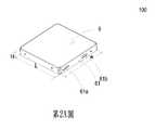
請參閱第2A圖至第2C圖所示,本案提供一種微粒偵測模組100,包含一基座1、一壓電致動器2、一驅動電路板3、一雷射組件4、一微粒傳感器5及一外蓋6,而基座1、壓電致動器2、驅動電路板3、雷射組件4、微粒傳感器5及外蓋6係以微小材料製出之模組結構,且該模組結構具有一長度、一寬度及一高度,其中模組結構之長度、寬度及高度介於1釐米(mm)至999釐米(mm)之間,或者介於1微米(μm)至999微米(μm)之間,或者介於1奈米(nm)至999奈米(nm)之間,但不以此為限。於本實施例中,基座1、壓電致動器2、驅動電路板3、雷射組件4、微粒傳感器5及外蓋6所構成之該模組結構具有其長度介於1微米至999微米、寬度介於1微米至999微米以及高度介於1微米至999微米時所構成的體積,或者模組結構具有其長度介於1奈米至999奈米、寬度介於1奈米至999奈米以及高度介於1奈米至999奈米時所構成的體積,但不以此為限。其中,驅動電路板3封蓋貼合於基座1的第二表面12,雷射組件4設置於驅動電路板3上,並與驅動電路板3電性連接,微粒傳感器5亦設置於驅動電路板3上,並與驅動電路板3電性連接,而外蓋6為罩蓋基座1,且貼附封蓋於基座1的第一表面11上,又外蓋6具有一側板61,側板61具有一進氣框口61a及出氣框口61b。Please refer to Figs. 2A to 2C. The present invention provides aparticle detection module 100, which includes abase 1, apiezoelectric actuator 2, adriving circuit board 3, alaser component 4, and a particle Thesensor 5 and anouter cover 6, and thebase 1, thepiezoelectric actuator 2, thedrive circuit board 3, thelaser component 4, theparticle sensor 5 and theouter cover 6 are modular structures made of tiny materials, and the The module structure has a length, a width and a height. The length, width and height of the module structure are between 1 centimeter (mm) and 999 centimeters (mm), or between 1 micrometer (μm) and 999 micrometers (μm), or between 1 nanometer (nm) and 999 nanometers (nm), but not limited to this. In this embodiment, the module structure composed of thebase 1, thepiezoelectric actuator 2, thedriving circuit board 3, thelaser component 4, theparticle sensor 5 and theouter cover 6 has a length ranging from 1 micron to 999 The volume constituted when the micron, the width is between 1 micron and 999 microns, and the height is between 1 micron and 999 microns, or the module structure has a length between 1 nanometer and 999 nanometers and a width between 1 nanometer and 999 Nanometer and the volume formed when the height is between 1 nanometer and 999 nanometers, but not limited to this. Wherein, thedriving circuit board 3 is covered and attached to thesecond surface 12 of thebase 1, thelaser assembly 4 is arranged on thedriving circuit board 3 and is electrically connected to thedriving circuit board 3, and theparticle sensor 5 is also arranged in the driving circuit On theboard 3 and electrically connected with thedriving circuit board 3, theouter cover 6 covers thebase 1 and is attached and sealed on thefirst surface 11 of thebase 1. Theouter cover 6 has aside plate 61, Theside plate 61 has an air inlet frame opening 61a and an air outlet frame opening 61b.

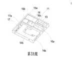
請審閱第3A圖及第3B圖所示,基座1具有一第一表面11、一第二表面12、一雷射設置區13、一進氣溝槽14、一導氣組件承載區15及一出氣溝槽16,第一表面11及第二表面12為相對設置之兩個表面,雷射設置區13自第一表面11朝向第二表面12挖空形成,進氣溝槽14自第二表面12凹陷形成,且鄰近雷射設置區13,進氣溝槽14設有一進氣口14a,連通於基座1的外部,並與外蓋6的進氣框口61a對應,以及兩側壁貫穿一透光窗口14b,與雷射設置區13連通;因此,基座1的第一表面11被外蓋6貼附封蓋,第二表面12被驅動電路板3貼附封蓋,致使進氣溝槽14定義出一進氣路徑。Please refer to Figures 3A and 3B. As shown in Figures 3A and 3B, thebase 1 has afirst surface 11, asecond surface 12, alaser setting area 13, anair inlet groove 14, an air guidecomponent bearing area 15 and Anair outlet groove 16, thefirst surface 11 and thesecond surface 12 are two opposite surfaces, thelaser setting area 13 is hollowed out from thefirst surface 11 to thesecond surface 12, and theair inlet groove 14 is formed from the second surface. Thesurface 12 is recessed and is adjacent to thelaser setting area 13. Theair inlet groove 14 is provided with anair inlet 14a, which communicates with the outside of thebase 1 and corresponds to the air inlet frame opening 61a of theouter cover 6, and the two side walls penetrate A light-transmittingwindow 14b communicates with thelaser setting area 13; therefore, thefirst surface 11 of thebase 1 is covered by theouter cover 6, and thesecond surface 12 is covered by thedrive circuit board 3, causing air intake Thegroove 14 defines an air intake path.

導氣組件承載區15由第二表面12凹陷形成,並連通進氣溝槽14,且於底面貫通一通氣孔15a;出氣溝槽16設有一出氣口16a,出氣口16a與外蓋6的出氣框口61b對應設置,出氣溝槽16包含由第一表面11對應於導氣組件承載區15的垂直投影區域凹陷形成的一第一區間16b,以及於非導氣組件承載區15的垂直投影區域所延伸的區域,且由第一表面11至第二表面12挖空形成的第二區間16c,其中第一區間16b與第二區間16c相連以形成段差,且出氣溝槽16的第一區間16b與導氣組件承載區15的通氣孔15a相通,出氣溝槽16的第二區間16c與出氣口16a連通;因此,當基座1的第一表面11被外蓋6貼附封蓋,第二表面12被驅動電路板3貼附封蓋時,致使出氣溝槽16定義出一出氣路徑。The air guidecomponent bearing area 15 is formed by recessing thesecond surface 12 and communicates with theair inlet groove 14 and penetrates avent hole 15a on the bottom surface; theair outlet groove 16 is provided with anair outlet 16a, theair outlet 16a and the air outlet frame of theouter cover 6 The opening 61b is correspondingly arranged, and theair outlet groove 16 includes afirst area 16b recessed and formed by the vertical projection area of thefirst surface 11 corresponding to the air guidecomponent bearing area 15, and is formed in the vertical projection area of the non-air guidecomponent bearing area 15 An extended area, and asecond section 16c hollowed out from thefirst surface 11 to thesecond surface 12, wherein thefirst section 16b and thesecond section 16c are connected to form a step difference, and thefirst section 16b of theair outlet groove 16 is Thevent hole 15a of the air guideassembly carrying area 15 communicates, and thesecond section 16c of theair outlet groove 16 communicates with theair outlet 16a; therefore, when thefirst surface 11 of thebase 1 is covered by theouter cover 6, thesecond surface 12 When the cover is attached to thedriving circuit board 3, theair outlet groove 16 defines an air outlet path.

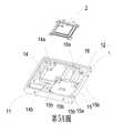
第4圖為基座容置雷射組件及微粒傳感器示意圖,雷射組件4及微粒傳感器5皆設置於驅動電路板3上且於基座1內,為了明確說明雷射組件4及微粒傳感器5與基座1之位置,故特意於第3圖中省略驅動電路板3,用以明確說明;請審閱第4圖及第2C圖,雷射組件4將容設於基座1的雷射設置區13內,微粒傳感器5容設於基座1的進氣溝槽14內,並與雷射組件4對齊,此外,雷射組件4對應到透光窗口14b,供以雷射組件4所發射的雷射光穿過,使雷射光照射至進氣溝槽14內,而雷射組件4所發出射出之光束路徑為穿過透光窗口14b且與進氣溝槽14形成正交方向。Figure 4 is a schematic diagram of the base accommodating the laser assembly and the particle sensor. Thelaser assembly 4 and theparticle sensor 5 are both arranged on thedrive circuit board 3 and in thebase 1, in order to clearly illustrate thelaser assembly 4 and theparticle sensor 5. The position of thebase 1 and thedrive circuit board 3 is omitted in Figure 3 for clear explanation; please refer to Figures 4 and 2C, thelaser assembly 4 will be accommodated in the laser setting of thebase 1. Inarea 13, theparticle sensor 5 is accommodated in theair inlet groove 14 of thebase 1 and aligned with thelaser assembly 4. In addition, thelaser assembly 4 corresponds to thelight transmission window 14b for thelaser assembly 4 to emit The laser light passing through makes the laser light irradiate into theair inlet groove 14, and the beam path emitted by thelaser assembly 4 passes through thetransparent window 14 b and forms an orthogonal direction with theair inlet groove 14.

雷射組件4發射投射光束通過透光窗口14b進入進氣溝槽14內,照射進氣溝槽14內的氣體中所含懸浮微粒,光束接觸到懸浮微粒時,會散射並產生投射光點,微粒傳感器5接收散射所產生的投射光點進行計算,來獲取氣體中所含懸浮微粒之粒徑及濃度的相關資訊。其中微粒傳感器5為PM2.5傳感器。Thelaser assembly 4 emits a projected light beam through the light-transmittingwindow 14b into theair inlet groove 14 to illuminate the suspended particles contained in the gas in theair inlet groove 14. When the light beam contacts the suspended particles, it will scatter and generate a projected light spot. Theparticle sensor 5 receives the projected light points generated by the scattering and performs calculations to obtain information about the particle size and concentration of the suspended particles contained in the gas. Theparticle sensor 5 is a PM2.5 sensor.

請參閱第5A圖及第5B圖,壓電致動器2容設於基座1的導氣組件承載區15,導氣組件承載區15呈一正方形,其四個角分別設有一定位缺口15b,壓電致動器2通過四個定位缺口15b設置於導氣組件承載區15內,此外,導氣組件承載區15與進氣溝槽14相通,當壓電致動器2作動時,汲取進氣溝槽14內的氣體進入壓電致動器2,並將氣體通過導氣組件承載區15的通氣孔15a,進入至出氣溝槽16。Please refer to Figures 5A and 5B, thepiezoelectric actuator 2 is accommodated in the air guidecomponent carrying area 15 of thebase 1. The air guidecomponent carrying area 15 is a square, and its four corners are respectively provided with apositioning notch 15b , Thepiezoelectric actuator 2 is arranged in the air guideassembly carrying area 15 through fourpositioning notches 15b. In addition, the air guideassembly carrying area 15 is in communication with theair inlet groove 14. When thepiezoelectric actuator 2 is actuated, it draws The gas in thegas inlet groove 14 enters thepiezoelectric actuator 2, and the gas enters thegas outlet groove 16 through thevent hole 15 a of the air guideassembly carrying area 15.

請審閱第6A圖及第6B圖,壓電致動器2包含有:一噴氣孔片21、一腔體框架22、一致動體23、一絕緣框架24及一導電框架25。Please refer to FIGS. 6A and 6B. Thepiezoelectric actuator 2 includes: ajet hole sheet 21, acavity frame 22, anactuator 23, aninsulating frame 24, and aconductive frame 25.

噴氣孔片21為具有可撓性之材料製作,具有一懸浮片210、一中空孔洞211以及複數個連接件212。懸浮片210為可彎曲振動之片狀結構,其形狀與尺寸大致對應導氣組件承載區15的內緣,但不以此為限,懸浮片210之形狀亦可為方形、圓形、橢圓形、三角形及多角形其中之一。中空孔洞211係貫穿於懸浮片210之中心處,以供氣體流通。本實施例中,連接件212之數量係為四個,其數量及型態主要與導氣組件承載區15的定位缺口15b相互對應,各連接件212與所對應之定位缺口15b會形成一卡扣結構藉以相互卡合、固定,使壓電致動器2得以設置於導氣組件承載區15內。The airjet hole sheet 21 is made of a flexible material and has asuspension sheet 210, ahollow hole 211 and a plurality of connectingmembers 212. Thefloating piece 210 is a sheet-like structure capable of bending and vibrating, and its shape and size roughly correspond to the inner edge of the air guidecomponent bearing area 15, but not limited to this. The shape of thefloating piece 210 can also be square, round, or oval. One of, triangle and polygon. Thehollow hole 211 penetrates through the center of the suspendedsheet 210 for gas flow. In this embodiment, the number of connectingpieces 212 is four, and the number and type of the connectingpieces 212 mainly correspond to thepositioning notches 15b of the air guidecomponent carrying area 15. Each connectingpiece 212 and thecorresponding positioning notch 15b will form a card. The buckle structure is mutually engaged and fixed, so that thepiezoelectric actuator 2 can be arranged in the air guideassembly carrying area 15.

腔體框架22疊設於噴氣孔片21,且其外型與噴氣孔片21對應,致動體23疊設於腔體框架22上,並與腔體框架22、懸浮片210之間定義一共振腔室26,絕緣框架24疊設於致動體23,其外觀與腔體框架22近似,導電框架25疊設於絕緣框架24,其外觀與絕緣框架24近似,且導電框架25具有一導電接腳251及一導電電極252,導電接腳251自導電框架25的外緣向外延伸,導電電極252自導電框架25內緣向內延伸。此外,致動體23更包含有一壓電載板231、一調整共振板232及一壓電板233,壓電載板231承載疊置於腔體框架22上,調整共振板232承載疊置於壓電載板231上,壓電板233承載疊置於調整共振板232上,而調整共振板232及壓電板233容設於絕緣框架24內,並由導電框架25的導電電極252電連接壓電板233,其中,壓電載板231、調整共振板232皆為可導電的材料所製成,壓電載板231具有一壓電接腳2311,壓電接腳2311與導電接腳251連接驅動電路板3上的驅動電路(未圖示),以接收驅動訊號(驅動頻率及驅動電壓),驅動訊號得以由壓電接腳2311、壓電載板231、調整共振板232、壓電板233、導電電極252、導電框架25、導電接腳251形成一迴路,並由絕緣框架24將導電框架25與致動體23之間阻隔,避免短路發生,使驅動訊號得以傳遞至壓電板233,壓電板233接受驅動訊號(驅動頻率及驅動電壓)後,因壓電效應產生形變,來進一步驅動壓電載板231及調整共振板232產生往復式地彎曲振動。Thecavity frame 22 is stacked on the air-jet orifice sheet 21, and its shape corresponds to the air-jet orifice sheet 21, and theactuator 23 is stacked on thecavity frame 22 and defines a space between thecavity frame 22 and thesuspension sheet 210 In theresonance chamber 26, theinsulating frame 24 is stacked on the actuatingbody 23, and its appearance is similar to thecavity frame 22, and theconductive frame 25 is stacked on theinsulating frame 24, and its appearance is similar to theinsulating frame 24, and theconductive frame 25 has a conductive Thepin 251 and aconductive electrode 252 extend outward from the outer edge of theconductive frame 25, and theconductive electrode 252 extends inward from the inner edge of theconductive frame 25. In addition, the actuatingbody 23 further includes apiezoelectric carrier plate 231, an adjustingresonance plate 232, and apiezoelectric plate 233. Thepiezoelectric carrier plate 231 is stacked on thecavity frame 22, and the adjustingresonance plate 232 is stacked on thecavity frame 22. On thepiezoelectric carrier plate 231, thepiezoelectric plate 233 is supported and stacked on the adjustingresonance plate 232, and the adjustingresonance plate 232 and thepiezoelectric plate 233 are housed in theinsulating frame 24 and electrically connected by theconductive electrode 252 of theconductive frame 25 Thepiezoelectric plate 233, wherein thepiezoelectric carrier plate 231 and the adjustingresonance plate 232 are all made of conductive materials. Thepiezoelectric carrier plate 231 has apiezoelectric pin 2311, apiezoelectric pin 2311 and aconductive pin 251 Connect the drive circuit (not shown) on thedrive circuit board 3 to receive the drive signal (drive frequency and drive voltage). The drive signal can be transmitted from thepiezoelectric pin 2311, thepiezoelectric carrier 231, theadjustment resonance board 232, and the piezoelectric Theplate 233, theconductive electrodes 252, theconductive frame 25, and theconductive pins 251 form a loop, and theinsulating frame 24 blocks theconductive frame 25 and theactuator 23 to avoid short circuits and enable the driving signal to be transmitted to thepiezoelectric plate 233. After receiving the driving signal (driving frequency and driving voltage), thepiezoelectric plate 233 deforms due to the piezoelectric effect to further drive thepiezoelectric carrier plate 231 and adjust theresonance plate 232 to generate reciprocating bending vibration.

承上所述,調整共振板232位於壓電板233與壓電載板231之間,作為兩者之間的緩衝物,可調整壓電載板231的振動頻率。基本上,調整共振板232的厚度大於壓電載板231的厚度,且調整共振板232的厚度可變動,藉此調整致動體23的振動頻率。As mentioned above, the adjustingresonance plate 232 is located between thepiezoelectric plate 233 and thepiezoelectric carrier plate 231, as a buffer between the two, and can adjust the vibration frequency of thepiezoelectric carrier plate 231. Basically, the thickness of the adjustingresonance plate 232 is greater than the thickness of thepiezoelectric carrier 231, and the thickness of the adjustingresonance plate 232 can be changed, thereby adjusting the vibration frequency of the actuatingbody 23.

請同時參閱第6A圖、第6B圖及第7A圖,複數個連接件212在懸浮片210及導氣組件承載區15的內緣之間定義出複數個空隙213,以供氣體流通。Please refer to FIG. 6A, FIG. 6B and FIG. 7A at the same time. The plurality of connectingmembers 212 define a plurality ofgaps 213 between the floatingpiece 210 and the inner edge of the air guidecomponent carrying area 15 for gas flow.

請先參閱第7A圖,噴氣孔片21、腔體框架22、致動體23、絕緣框架24及導電框架25依序對應堆疊並設置於導氣組件承載區15,噴氣孔片21與導氣組件承載區15之底面(未標示)之間形成一氣流腔室27。氣流腔室27透過噴氣孔片21之中空孔洞211,連通致動體23、腔體框架22及懸浮片210之間的共振腔室26。透過控制共振腔室26中氣體之振動頻率,使其與懸浮片210之振動頻率趨近於相同,可使共振腔室26與懸浮片210產生亥姆霍茲共振效應(Helmholtz resonance),俾使氣體傳輸效率提高。Please refer to Figure 7A first, the airjet orifice sheet 21, thecavity frame 22, the actuatingbody 23, the insulatingframe 24 and theconductive frame 25 are sequentially stacked and arranged in the air guideassembly carrying area 15, and the airjet orifice sheet 21 and the air guide Anair flow chamber 27 is formed between the bottom surfaces (not labeled) of thecomponent carrying area 15. Theair flow chamber 27 penetrates thehollow hole 211 in the airjet orifice sheet 21 to communicate with theresonance chamber 26 between the actuatingbody 23, thecavity frame 22 and thesuspension sheet 210. By controlling the vibration frequency of the gas in theresonance chamber 26 so that it is close to the vibration frequency of thesuspension plate 210, theresonance chamber 26 and thesuspension plate 210 can produce Helmholtz resonance effect (Helmholtz resonance). The gas transmission efficiency is improved.

第7B圖及第7C圖為第7A圖之壓電致動器作動示意圖,請先審閱第7B圖所示,當壓電板233向遠離導氣組件承載區15之底面移動時,帶動噴氣孔片21之懸浮片210以遠離導氣組件承載區15之底面方向移動,使氣流腔室27之容積急遽擴張,其內部壓力下降形成負壓,吸引壓電致動器2外部的氣體由複數個空隙213流入,並經由中空孔洞211進入共振腔室26,使共振腔室26內的氣壓增加而產生一壓力梯度。再如第7C圖所示,當壓電板233帶動噴氣孔片21之懸浮片210朝向導氣組件承載區15之底面移動時,共振腔室26中的氣體經中空孔洞211快速流出,擠壓氣流腔室27內的氣體,並使匯聚後之氣體以接近白努利定律之理想氣體狀態快速且大量地噴出。依據慣性原理,排氣後的共振腔室26內部氣壓低於平衡氣壓,會導引氣體再次進入共振腔室26中。是以,透過重複第7B圖及第7C圖的動作後,得以壓電板233往復式地振動,以及控制共振腔室26中氣體之振動頻率與壓電板233之振動頻率趨近於相同,以產生亥姆霍茲共振效應,俾實現氣體高速且大量的傳輸。Figures 7B and 7C are schematic diagrams of the action of the piezoelectric actuator in Figure 7A. Please review Figure 7B. When thepiezoelectric plate 233 moves to the bottom surface away from the air guidecomponent bearing area 15, it drives the air injection hole The floatingpiece 210 of thepiece 21 moves in a direction away from the bottom surface of the air guideassembly carrying area 15, so that the volume of theair flow chamber 27 is rapidly expanded, and its internal pressure drops to form a negative pressure, which attracts the air outside thepiezoelectric actuator 2 by a plurality of Thegap 213 flows in and enters theresonance chamber 26 through thehollow hole 211, so that the air pressure in theresonance chamber 26 increases to generate a pressure gradient. As shown in Fig. 7C again, when thepiezoelectric plate 233 drives the suspendingpiece 210 of the airjet orifice plate 21 to move toward the bottom surface of the air guideassembly carrying area 15, the gas in theresonance chamber 26 flows out quickly through thehollow hole 211, squeezing The gas in thegas flow chamber 27 and the collected gas are ejected quickly and in large quantities in an ideal gas state close to Bernoulli's law. According to the principle of inertia, the air pressure inside theresonance chamber 26 after exhaust is lower than the equilibrium pressure, which will guide the gas to enter theresonance chamber 26 again. Therefore, by repeating the actions shown in Figures 7B and 7C, thepiezoelectric plate 233 can vibrate reciprocally, and the vibration frequency of the gas in theresonance chamber 26 is controlled to approach the vibration frequency of thepiezoelectric plate 233. In order to generate the Helmholtz resonance effect, to achieve high-speed and large-scale gas transmission.

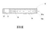
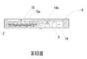
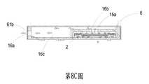
請參閱第8A圖至第8C圖,第8A圖至第8C圖為微粒偵測模組的氣體路徑示意圖,首先審閱第8A圖,氣體皆由外蓋6的進氣框口61a進入,通過進氣口14a進入至基座1的進氣溝槽14,並流至微粒傳感器5的位置,再如第8B圖所示,壓電致動器2持續驅動會吸取進氣路徑之氣體,以利外部氣體快速導入且穩定流通,並通過微粒傳感器5上方,此時雷射組件4發射投射光束通過透光窗口14b進入進氣溝槽14內,照射進氣溝槽14通過微粒傳感器5上方的氣體中所含懸浮微粒,光束接觸到懸浮微粒時,會散射並產生投射光點,微粒傳感器5接收散射所產生的投射光點進行計算,來獲取氣體中所含懸浮微粒之粒徑及濃度的相關資訊,而微粒傳感器5上方的氣體也持續受壓電致動器2驅動傳輸而導入導氣組件承載區15的通氣孔15a中,進入出氣溝槽16的第一區間16b,最後如第8C圖所示,氣體進入出氣溝槽16的第一區間16b後,由於壓電致動器2會不斷輸送氣體進入第一區間16b,於第一區間16b的氣體將會被推引至第二區間16c,最後通過出氣口16a及出氣框口61b向外排出。Please refer to Figs. 8A to 8C. Figs. 8A to 8C are schematic diagrams of the gas path of the particle detection module. First, review Fig. 8A. The gas enters from theinlet frame port 61a of theouter cover 6, and passes through the inlet Theair port 14a enters theair inlet groove 14 of thebase 1 and flows to the position of theparticle sensor 5. As shown in Fig. 8B, thepiezoelectric actuator 2 continues to drive to absorb the air in the air inlet path to facilitate The external air is quickly introduced and circulates stably, and passes over theparticle sensor 5. At this time, thelaser assembly 4 emits a projected beam into theair inlet groove 14 through the light-transmittingwindow 14b, and illuminates the air that passes through theair inlet groove 14 through theparticle sensor 5 When the light beam touches the suspended particles, it will scatter and produce a projected light point. Theparticle sensor 5 receives the projected light point generated by the scattering and calculates to obtain the correlation between the particle size and concentration of the suspended particle in the gas Information, and the gas above theparticle sensor 5 is continuously driven and transmitted by thepiezoelectric actuator 2 to be introduced into thevent hole 15a of the air guideassembly carrying area 15, and into thefirst section 16b of thegas outlet groove 16, as shown in Fig. 8C As shown, after the gas enters thefirst section 16b of thegas outlet groove 16, since thepiezoelectric actuator 2 will continuously deliver the gas into thefirst section 16b, the gas in thefirst section 16b will be pushed to thesecond section 16c , And finally exhaust through theair outlet 16a and theair outlet frame 61b.

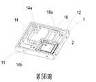
如第9圖所示,基座1更包含有一光陷阱區17,光陷阱區17自第一表面11至第二表面12挖空形成,並對應至雷射設置區13,且光陷阱區17經過透光窗口14b而使雷射組件4所發射之光束能投射到其中,光陷阱區17設有一斜椎面之光陷阱結構17a,光陷阱結構17a對應到雷射組件4所發射之光束的路徑;此外,光陷阱結構17a使雷射組件4所發射之投射光束在斜椎面結構反射至光陷阱區17內,避免光束反射至微粒傳感器5的位置,且光陷阱結構17a所接收之投射光束之位置與透光窗口14b之間保持有一光陷阱距離D,此光陷阱距離D需大於3mm以上,當光陷阱距離D小於3mm時會導致投射在光陷阱結構17a上投射光束反射後因過多雜散光直接反射回微粒傳感器5的位置,造成偵測精度的失真。As shown in FIG. 9, thebase 1 further includes alight trap area 17. Thelight trap area 17 is hollowed out from thefirst surface 11 to thesecond surface 12 and corresponds to thelaser setting area 13, and thelight trap area 17 The light beam emitted by thelaser assembly 4 can be projected through the light-transmittingwindow 14b. Thelight trap area 17 is provided with an oblique cone-shapedlight trap structure 17a. Thelight trap structure 17a corresponds to the light beam emitted by thelaser assembly 4 Path; In addition, thelight trap structure 17a makes the projected light beam emitted by thelaser assembly 4 reflected in the oblique cone structure to thelight trap area 17, to prevent the light beam from being reflected to the position of theparticle sensor 5, and thelight trap structure 17a receives the projection There is a light trap distance D between the position of the light beam and the light-transmittingwindow 14b. The light trap distance D must be greater than 3mm. When the light trap distance D is less than 3mm, the projected light beam will be projected on thelight trap structure 17a due to excessive reflection. The stray light is directly reflected back to the position of theparticle sensor 5, causing distortion of the detection accuracy.

請繼續審閱第9圖及第2C圖,本案之微粒偵測模組100,不僅可針對氣體中微粒進行偵測,更可進一步針對導入氣體之特性做偵測,因此本案之微粒偵測模組100更包含有第一揮發性有機物傳感器7a,定位設置於驅動電路板3上並與其電性連接,容設於出氣溝槽16中,對出氣路徑所導出氣體做偵測,用以偵測出氣路徑的氣體中所含有之揮發性有機物的濃度。或者本案之微粒偵測模組100更包含有一第二揮發性有機物傳感器7b,定位設置於驅動電路板3上並與其電性連接,而第二揮發性有機物傳感器7b容設於光陷阱區17,對於通過進氣溝槽14的進氣路徑且經過透光窗口14b而導入光陷阱區17內的氣體偵測其揮發性有機物的濃度。Please continue to review Figure 9 and Figure 2C. Theparticle detection module 100 in this case can not only detect particles in the gas, but also detect the characteristics of the introduced gas. Therefore, the particle detection module in thiscase 100 further includes a first volatileorganic compound sensor 7a, which is positioned and electrically connected to the drivingcircuit board 3, and is accommodated in thegas outlet groove 16 to detect the gas derived from the gas outlet path to detect the gas The concentration of volatile organic compounds contained in the gas in the path. Or theparticle detection module 100 in this case further includes a second volatileorganic compound sensor 7b positioned and electrically connected to the drivingcircuit board 3, and the second volatileorganic compound sensor 7b is accommodated in thelight trap area 17. The concentration of the volatile organic compounds of the gas introduced into thelight trap area 17 through the air inlet path of theair inlet groove 14 and thetransparent window 14b is detected.

由上述說明可知,本案的微粒偵測模組100經過基座1上雷射設置區13、進氣溝槽14、導氣組件承載區15及出氣溝槽16適當配置的結構設計,且搭配外蓋6及驅動電路板3之封蓋密封設計,致使基座1之第一表面11上罩蓋外蓋6,第二表面12上封蓋驅動電路板3,以使進氣溝槽14定義出一進氣路徑,出氣溝槽16定義出一出氣路徑,形成一單層導氣通道路徑,讓本案的微粒偵測模組100整體結構之高度降低,致使微粒偵測模組100的長度L介於10mm至35mm之間,寬度W介於10mm至35mm之間,厚度H介於1mm至6.5mm之間,有利於組設結合於如第12圖所示的小型化可攜式電子裝置2A,或者有利於組設結合於如第13圖所示的小型化行動裝置3A,便於使用者攜帶以偵測周遭的微粒濃度。此外,本案的壓電致動器2的另一實施例可為一微機電泵浦2a,請參閱第10A圖及第10B圖,微機電泵浦2a包含有一第一基板21a、一第一氧化層22a、一第二基板23a以及一壓電組件24a。It can be seen from the above description that theparticle detection module 100 in this case passes through the structural design of thelaser setting area 13, theair inlet groove 14, the air guidecomponent bearing area 15 and theair outlet groove 16 on thebase 1, and is properly configured with external The sealing design of thecover 6 and the drivingcircuit board 3 causes thefirst surface 11 of thebase 1 to cover theouter cover 6, and thesecond surface 12 to cover thedriving circuit board 3 so that theair inlet groove 14 is defined An air inlet path, and theair outlet groove 16 defines an air outlet path, forming a single-layer air guiding channel path, so that the height of the overall structure of theparticle detection module 100 in this case is reduced, so that the length L of theparticle detection module 100 is medium Between 10mm and 35mm, the width W is between 10mm and 35mm, and the thickness H is between 1mm and 6.5mm, which facilitates the assembly and integration of the miniaturized portableelectronic device 2A as shown in Figure 12. Or it is advantageous for the assembly to be combined with the miniaturized mobile device 3A as shown in FIG. 13, which is convenient for the user to carry to detect the particle concentration around. In addition, another embodiment of thepiezoelectric actuator 2 in this case can be amicroelectromechanical pump 2a. Please refer to FIG. 10A and FIG. 10B. Themicroelectromechanical pump 2a includes afirst substrate 21a and a first oxide. Thelayer 22a, asecond substrate 23a and apiezoelectric component 24a.

第一基板21a為一矽晶片(Si wafer),其厚度介於150至400微米(μm)之間,第一基板21a具有複數個流入孔211a、一第一表面212a、一第二表面213a,於本實施例中,該些流入孔211a的數量為4個,但不以此為限,且每個流入孔211a皆由第二表面213a貫穿至第一表面212a,而流入孔211a為了提升流入效果,將流入孔211a自第二表面213a至第一表面212a呈現漸縮的錐形。Thefirst substrate 21a is a silicon wafer (Si wafer) with a thickness of 150 to 400 microns (μm). Thefirst substrate 21a has a plurality ofinflow holes 211a, afirst surface 212a, and asecond surface 213a. In this embodiment, the number of theinflow holes 211a is four, but it is not limited to this, and eachinflow hole 211a penetrates from thesecond surface 213a to thefirst surface 212a, and theinflow hole 211a is used to enhance the inflow As a result, theinflow hole 211a is tapered from thesecond surface 213a to thefirst surface 212a.

第一氧化層22a為一二氧化矽(SiO2)薄膜,其厚度介於10至20微米(μm)之間,第一氧化層22a疊設於第一基板21a的第一表面212a上,第一氧化層22a具有複數個匯流通道221a以及一匯流腔室222a,匯流通道221a與第一基板21a的流入孔211a其數量及位置相互對應。於本實施例中,匯流通道221a的數量同樣為4個,4個匯流通道221a的一端分別連通至第一基板21a的4個流入孔211a,而4個匯流通道221a的另一端則連通於匯流腔室222a,讓氣體分別由流入孔211a進入之後,通過其對應相連之匯流通道221a後匯聚至匯流腔室222a內。Thefirst oxide layer 22a is a silicon dioxide (SiO2 ) film with a thickness between 10 and 20 microns (μm). Thefirst oxide layer 22a is stacked on thefirst surface 212a of thefirst substrate 21a. Theoxide layer 22a has a plurality offlow channels 221a and aflow chamber 222a. The number and positions of theflow channels 221a and theinflow holes 211a of thefirst substrate 21a correspond to each other. In this embodiment, the number of theconfluence channels 221a is also four, one end of the fourconfluence channels 221a is respectively connected to the fourinflow holes 211a of thefirst substrate 21a, and the other end of the fourconfluence channels 221a is connected to the confluence Thechamber 222a allows gas to enter through theinflow holes 211a, and then converge into theconfluence chamber 222a after passing through thecorresponding confluence channels 221a.

第二基板23a為一絕緣層上覆矽之矽晶片(SOI wafer),包含有:一矽晶片層231a、一第二氧化層232a以及一矽材層233a;矽晶片層231a的厚度介於10至20微米(μm)之間,具有一致動部2311a、一外周部2312a、複數個連接部2313a以及複數個流體通道2314a,致動部2311a呈圓形;外周部2312a呈中空環狀,環繞於致動部2311a的外圍;該些連接部2313a分別位於致動部2311a與外周部2312a之間,並且連接兩者,提供彈性支撐的功能。該些流體通道2314a環繞形成於致動部2311a的外圍,且分別位於該些連接部2313a之間。Thesecond substrate 23a is a silicon-on-insulating silicon wafer (SOI wafer), including: asilicon wafer layer 231a, asecond oxide layer 232a, and asilicon material layer 233a; the thickness of thesilicon wafer layer 231a is between 10 To 20 microns (μm), there is anactuating portion 2311a, an outerperipheral portion 2312a, a plurality of connectingportions 2313a and a plurality offluid channels 2314a, theactuating portion 2311a is circular; the outerperipheral portion 2312a is a hollow ring, surrounding The periphery of theactuating portion 2311a; the connectingportions 2313a are respectively located between the actuatingportion 2311a and the outerperipheral portion 2312a, and connect the two to provide the function of elastic support. Thefluid channels 2314a are formed around the periphery of theactuating portion 2311a and are located between the connectingportions 2313a.

第二氧化層232a為一氧化矽層其厚度介於0.5至2微米(μm)之間,形成於矽晶片層231a上,呈中空環狀,並與矽晶片層231a定義一振動腔室2321a。矽材層233a呈圓形,疊設於第二氧化層232a且結合至第一氧化層22a,矽材層233a為二氧化矽(SiO2)薄膜,厚度介於2至5微米(μm)之間,具有一穿孔2331a、一振動部2332a、一固定部2333a、一第三表面2334a及一第四表面2335a。穿孔2331a形成於矽材層233a的中心,振動部2332a位於穿孔2331a的周邊區域,且垂直對應於振動腔室2321a,固定部2333a則為矽材層233a的周緣區域,由固定部2333a固定於第二氧化層232a,第三表面2334a與第二氧化層232a接合,第四表面2335a與第一氧化層22a接合;壓電組件24a疊設於矽晶片層231a的致動部2311a。Thesecond oxide layer 232a is a silicon oxide layer with a thickness between 0.5 and 2 micrometers (μm). It is formed on thesilicon wafer layer 231a in a hollow ring shape and defines avibration chamber 2321a with thesilicon wafer layer 231a. Thesilicon material layer 233a has a circular shape and is stacked on thesecond oxide layer 232a and is bonded to thefirst oxide layer 22a. Thesilicon material layer 233a is a silicon dioxide (SiO2 ) film with a thickness of 2 to 5 microns (μm) There is a throughhole 2331a, a vibratingportion 2332a, a fixingportion 2333a, athird surface 2334a, and afourth surface 2335a. The throughhole 2331a is formed in the center of thesilicon material layer 233a, thevibration part 2332a is located in the peripheral area of the throughhole 2331a, and corresponds to thevibration chamber 2321a perpendicularly, and the fixingpart 2333a is the peripheral area of thesilicon material layer 233a, which is fixed to the second part by the fixingpart 2333a. Thethird surface 2334a is bonded to thesecond oxide layer 232a, and thefourth surface 2335a is bonded to thefirst oxide layer 22a. Thepiezoelectric element 24a is stacked on theactuating portion 2311a of thesilicon wafer layer 231a.

壓電組件24a包含有一下電極層241a、壓電層242a、絕緣層243a及上電極層244a,下電極層241a疊置於矽晶片層231a的致動部2311a,而壓電層242a疊置於下電極層241a,兩者透過其接觸的區域做電性連接,此外,壓電層242a的寬度小於下電極層241a的寬度,使得壓電層242a無法完全遮蔽住下電極層241a,再於壓電層242a的部分區域以及下電極層241a未被壓電層242a所遮蔽的區域上疊置絕緣層243a,最後再於絕緣層243a以及壓電層242a未被絕緣層243a遮蔽的其餘表面上疊置上電極層244a,讓上電極層244a得以與壓電層242a接觸來電性連接,同時利用絕緣層243a阻隔於上電極層244a及下電極層241a之間,避免兩者直接接觸造成短路。Thepiezoelectric component 24a includes abottom electrode layer 241a, apiezoelectric layer 242a, an insulatinglayer 243a, and anupper electrode layer 244a. Thebottom electrode layer 241a is stacked on theactuating portion 2311a of thesilicon wafer layer 231a, and thepiezoelectric layer 242a is stacked on Thelower electrode layer 241a is electrically connected through the contact area. In addition, the width of thepiezoelectric layer 242a is smaller than the width of thelower electrode layer 241a, so that thepiezoelectric layer 242a cannot completely cover thelower electrode layer 241a. An insulatinglayer 243a is stacked on a part of theelectrical layer 242a and the area of thelower electrode layer 241a not shielded by thepiezoelectric layer 242a, and finally on the insulatinglayer 243a and the remaining surface of thepiezoelectric layer 242a not shielded by the insulatinglayer 243a. Theupper electrode layer 244a is placed so that theupper electrode layer 244a can contact and electrically connect with thepiezoelectric layer 242a. At the same time, the insulatinglayer 243a is used to block theupper electrode layer 244a and thelower electrode layer 241a to avoid direct contact between the two and cause a short circuit.

請參考第11A至第11C圖,第11A至11C圖為微機電泵浦2a其作動示意圖。請先參考第11A圖,壓電組件24a的下電極層241a及上電極層244a接收驅動電路板3所傳遞之驅動電壓及驅動訊號(未圖示)後將其傳導至壓電層242a,壓電層242a接受驅動電壓及驅動訊號後,因逆壓電效應的影響開始產生形變,會帶動矽晶片層231a的致動部2311a開始位移,當壓電組件24a帶動致動部2311a向上位移並拉開與第二氧化層232a之間的距離時,此時,第二氧化層232a的振動腔室2321a的容積將提升,讓振動腔室2321a內形成負壓,並將第一氧化層22a的匯流腔室222a內的氣體通過穿孔2331a吸入其中。請繼續參閱第11B圖,當致動部2311a受到壓電組件24a的牽引向上位移時,矽材層233a的振動部2332a會因共振原理的影響向上位移,當振動部2332a向上位移時,會壓縮振動腔室2321a的空間並且推動振動腔室2321a內的氣體往矽晶片層231a的流體通道2314a移動,讓氣體能夠通過流體通道2314a向上排出,在振動部2332a向上位移來壓縮振動腔室2321a的同時,匯流腔室222a的容積因振動部2332a位移而提升,其內部形成負壓,將吸取微機電泵浦2a外的氣體由流入孔211a進入其中,最後如第11C圖所示,壓電組件24a帶動矽晶片層231a的致動部2311a向下位移時,將振動腔室2321a的氣體往流體通道2314a推動,並將氣體排出,而矽材層233a的振動部2332a亦受致動部2311a的帶動向下位移,同步壓縮匯流腔室222a的氣體通過穿孔2331a向振動腔室2321a移動,後續再將壓電組件24a帶動致動部2311a向上位移時,其振動腔室2321a的容積會大幅提升,進而有較高的汲取力將氣體吸入振動腔室2321a,再重複以上的動作,以至於透過壓電組件24a持續帶動致動部2311a上下位移來使振動部2332a連動並上下位移,透過改變微機電泵浦2a的內部壓力,使其不斷地汲取及排出氣體,藉此以完成微機電泵浦2a的動作。Please refer to Figures 11A to 11C. Figures 11A to 11C are schematic diagrams of the operation of themicroelectromechanical pump 2a. Please refer to FIG. 11A first, thelower electrode layer 241a and theupper electrode layer 244a of thepiezoelectric element 24a receive the driving voltage and driving signal (not shown) transmitted by the drivingcircuit board 3 and then conduct them to thepiezoelectric layer 242a. After theelectric layer 242a receives the driving voltage and the driving signal, it begins to deform due to the influence of the inverse piezoelectric effect, which will drive the actuatingportion 2311a of thesilicon wafer layer 231a to start to move. When thepiezoelectric element 24a drives theactuating portion 2311a to move upward and pull When the distance between thesecond oxide layer 232a and thesecond oxide layer 232a is opened, the volume of thevibration chamber 2321a of thesecond oxide layer 232a will increase, so that a negative pressure is formed in thevibration chamber 2321a, and the confluence of thefirst oxide layer 22a The gas in thechamber 222a is sucked into it through theperforation 2331a. Please continue to refer to Figure 11B. When theactuating portion 2311a is pulled upward by thepiezoelectric element 24a, the vibratingportion 2332a of thesilicon layer 233a will be displaced upward due to the principle of resonance. When the vibratingportion 2332a is displaced upward, it will compress The space of thevibration chamber 2321a and push the gas in thevibration chamber 2321a to move to thefluid channel 2314a of thesilicon wafer layer 231a, so that the gas can be discharged upward through thefluid channel 2314a, and thevibration part 2332a moves upward to compress thevibration chamber 2321a. , The volume of theconfluence chamber 222a is increased due to the displacement of the vibratingpart 2332a, and a negative pressure is formed inside, which will suck the gas outside themicroelectromechanical pump 2a into it through theinflow hole 211a. Finally, as shown in Figure 11C, thepiezoelectric component 24a When driving theactuating portion 2311a of thesilicon wafer layer 231a to move downward, the gas in the vibratingchamber 2321a is pushed to thefluid channel 2314a and discharged, and the vibratingportion 2332a of thesilicon layer 233a is also driven by theactuating portion 2311a Displacement downwards, the gas in the synchronouscompression confluence chamber 222a moves to thevibration chamber 2321a through theperforation 2331a, and when thepiezoelectric component 24a drives theactuation portion 2311a to move upward, the volume of thevibration chamber 2321a will be greatly increased, and then A higher suction force sucks the gas into thevibration chamber 2321a, and then repeats the above actions, so that thepiezoelectric component 24a continuously drives theactuation part 2311a to move up and down to make the vibratingpart 2332a interlock and move up and down. By changing the MEMS pump The internal pressure of thepump 2a causes it to continuously draw and discharge gas, thereby completing the action of theMEMS pump 2a.

當然,本案的微粒偵測模組100為了嵌設於行動裝置3A的應用,本案的壓電致動器2可以微機電泵浦2a之結構取代,使本案微粒偵測模組100的整體尺寸更進一步縮小,致使微粒偵測模組100的長度L、寬度W縮減至2mm至4mm之間、厚度H介於1mm至3.5mm之間,實施於現況薄型5mm厚度智慧型手機等行動裝置3A中,將測模組直接嵌設於智慧型手機上,供使用者能夠即時對周遭的空氣品質進行檢測。Of course, for the application of theparticle detection module 100 in this case to be embedded in the mobile device 3A, thepiezoelectric actuator 2 in this case can be replaced by the structure of themicro-electromechanical pump 2a, so that the overall size of theparticle detection module 100 in this case is larger. With further reduction, the length L and width W of theparticle detection module 100 are reduced to between 2mm and 4mm, and the thickness H is between 1mm and 3.5mm, which is implemented in the current mobile device 3A such as a thin 5mm thickness smartphone. The test module is directly embedded on the smart phone, so that the user can check the surrounding air quality in real time.

綜上所述,本案所提供之微粒偵測模組,雷射組件直接設置於驅動電路板,並由驅動電路板貼附基座的第二表面,且使基座的第一表面被外蓋貼附,進而使進氣溝槽定義出一進氣路徑,以及使出氣溝槽定義一出氣路徑,可以大幅減少微粒偵測模組的厚度,此外,將壓電致動器與雷射組件區隔設置,再輔以氣體通道的設計,可以避免壓電致動器於作動時干擾到雷射組件及微粒傳感器運作,又可以縮小微粒偵測模組的體積,其長度可縮小至10mm至35mm之間,寬度可縮減至10mm至35mm之間,厚度可降低至1mm至6.5mm之間,使本案的微粒偵測模組可以便於攜帶,並且再利用光陷阱區的光陷阱結構,得以減少雷射組件通過微粒傳感器的光束接觸基座本身後所產生的散射光線再度進入微粒傳感器內,能夠提升微粒傳感器的偵測效率,極具產業利用性及進步性。In summary, in the particle detection module provided in this case, the laser component is directly arranged on the driving circuit board, and the driving circuit board is attached to the second surface of the base, and the first surface of the base is covered by the outer cover Attach, so that the air inlet groove defines an air inlet path, and the air outlet groove defines an air outlet path, which can greatly reduce the thickness of the particle detection module. In addition, the piezoelectric actuator and the laser component area Separate arrangement, supplemented by the design of the gas channel, can prevent the piezoelectric actuator from interfering with the operation of the laser component and the particle sensor when the piezoelectric actuator is activated, and can reduce the volume of the particle detection module, and its length can be reduced to 10mm to 35mm The width can be reduced to between 10mm and 35mm, and the thickness can be reduced to between 1mm and 6.5mm, so that the particle detection module in this case can be easily carried, and the light trap structure in the light trap area can be reused to reduce lightning The scattered light generated by the radiation component after the light beam of the particle sensor contacts the base itself enters the particle sensor again, which can improve the detection efficiency of the particle sensor, which is extremely industrially usable and progressive.

1A:微粒偵測裝置 11A:殼體 12A:導氣件 1:基座 100:微粒偵測模組 11:第一表面 12:第二表面 13:雷射設置區 14:進氣溝槽 14a:進氣口 14b:透光窗口 15:導氣組件承載區 15a:通氣孔 15b:定位缺口 16:出氣溝槽 16a:出氣口 16b:第一區間 16c:第二區間 17:光陷阱區 17a:光陷阱結構 2:壓電致動器 2A:可攜式電子裝置 21:噴氣孔片 210:懸浮片 211:中空孔洞 212:連接件 213:空隙 22:腔體框架 23:致動體 231:壓電載板 2311:壓電接腳 232:調整共振板 233:壓電板 24:絕緣框架 25:導電框架 251:導電接腳 252:導電電極 26:共振腔室 27:氣流腔室 2a:微機電泵浦 21a:第一基板 211a:流入孔 212a:第一表面 213a:第二表面 22a:第一氧化層 221a:匯流通道 222a:匯流腔室 23a:第二基板 231a:矽晶片層 2311a:致動部 2312a:外周部 2313a:連接部 2314a:流體通道 232a:第二氧化層 2321a:振動腔室 233a:矽材層 2331a:穿孔 2332a:振動部 2333a:固定部 2334a:第三表面 2335a:第四表面 24a:壓電組件 241a:下電極層 242a:壓電層 243a:絕緣層 244a:上電極層 3:驅動電路板 3A:行動裝置 4:雷射組件 5:微粒傳感器 6:外蓋 61:側板 61a:進氣框口 61b:出氣框口 7a:第一揮發性有機物傳感器 7b:第二揮發性有機物傳感器 D:光陷阱距離 H:厚度 L:長度 W:寬度1A: Particle detection device 11A: Shell 12A: Air guide 1: base 100: Particle detection module 11: First surface 12: second surface 13: Laser setting area 14: intake groove 14a: Air inlet 14b: Transparent window 15: Air guide component bearing area 15a: vent 15b: Positioning gap 16: Vent groove 16a: air outlet 16b: The first interval 16c: second interval 17: Light trap area 17a: Light trap structure 2: Piezo actuator 2A: Portable electronic device 21: Air jet hole sheet 210: Suspended Film 211: Hollow Hole 212: Connector 213: Gap 22: cavity frame 23: Actuating body 231: Piezo Carrier 2311: Piezo pin 232: Adjust the resonance plate 233: Piezo Plate 24: insulated frame 25: Conductive frame 251: conductive pin 252: Conductive electrode 26: resonance chamber 27: Airflow chamber 2a: MEMS pump 21a: First substrate 211a: Inflow hole 212a: first surface 213a: second surface 22a: first oxide layer 221a: Confluence channel 222a: Confluence chamber 23a: second substrate 231a: silicon wafer layer 2311a: Actuation Department 2312a: Peripheral 2313a: connecting part 2314a: fluid channel 232a: second oxide layer 2321a: Vibration Chamber 233a: Silicon layer 2331a: Piercing 2332a: Vibration Department 2333a: fixed part 2334a: third surface 2335a: fourth surface 24a: Piezoelectric component 241a: lower electrode layer 242a: Piezoelectric layer 243a: insulating layer 244a: Upper electrode layer 3: drive circuit board 3A: Mobile device 4: Laser component 5: Particle sensor 6: Outer cover 61: side panel 61a: intake frame port 61b: Outlet frame mouth 7a: The first volatile organic compound sensor 7b: The second volatile organic compound sensor D: Light trap distance H: thickness L: length W: width

第1圖為先前技術中微粒偵測模組之立體示意圖。 第2A圖為本案微粒偵測模組之外觀立體示意圖。 第2B圖為本案微粒偵測模組另一角度之外觀立體示意圖。 第2C圖所示為本案微粒偵測模組之分解立體示意圖。 第3A圖為基座之立體示意圖。 第3B圖為基座另一角度之立體示意圖。 第4圖為基座容置雷射組件及微粒傳感器之立體示意圖。 第5A圖為壓電致動器結合基座之分解立體示意圖。 第5B圖為壓電致動器結合基座之立體示意圖。 第6A圖為壓電致動器之分解立體示意圖。 第6B圖為壓電致動器另一角度之分解立體示意圖。 第7A圖為壓電致動器之結合於導氣組件承載區之剖面示意圖。 第7B圖及第7C圖為第7A圖之壓電致動器作動之示意圖。 第8A圖至第8C圖為微粒偵測模組氣體路徑之示意圖。 第9圖為雷射組件發射之光束路徑之示意圖。 第10A圖為微機電泵浦之剖面示意圖。 第10B圖為微機電泵浦之分解示意圖。 第11A圖至第11C圖為微機電泵浦作動之示意圖。 第12圖為微粒監測模組組設應用於小型化可攜式電子裝置之示意圖。 第13圖為微粒監測模組嵌設應用於小型化行動裝置之示意圖。Figure 1 is a three-dimensional schematic diagram of a particle detection module in the prior art. Figure 2A is a three-dimensional schematic diagram of the appearance of the particle detection module in this case. Figure 2B is a perspective view of the appearance of the particle detection module from another angle. Figure 2C shows an exploded three-dimensional schematic diagram of the particle detection module of this case. Figure 3A is a perspective view of the base. Figure 3B is a perspective view of the base from another angle. Figure 4 is a three-dimensional schematic diagram of the base housing the laser component and the particle sensor. Figure 5A is an exploded perspective view of the piezoelectric actuator combined with the base. Figure 5B is a perspective view of the piezoelectric actuator combined with the base. Figure 6A is an exploded perspective view of the piezoelectric actuator. Figure 6B is an exploded perspective view of the piezoelectric actuator from another angle. Figure 7A is a schematic cross-sectional view of the piezoelectric actuator combined with the bearing area of the air guide element. Figures 7B and 7C are schematic diagrams of the action of the piezoelectric actuator in Figure 7A. 8A to 8C are schematic diagrams of the gas path of the particle detection module. Figure 9 is a schematic diagram of the beam path emitted by the laser component. Figure 10A is a schematic cross-sectional view of the MEMS pump. Figure 10B is an exploded schematic diagram of the MEMS pump. Figures 11A to 11C are schematic diagrams of MEMS pumping. Figure 12 is a schematic diagram of the application of the particle monitoring module assembly to a miniaturized portable electronic device. Figure 13 is a schematic diagram of a particle monitoring module embedded in a miniaturized mobile device.

100:微粒偵測模組100: Particle detection module

1:基座1: base

11:第一表面11: First surface

12:第二表面12: second surface

13:雷射設置區13: Laser setting area

14a:進氣口14a: Air inlet

14b:透光窗口14b: Transparent window

15a:通氣孔15a: vent

16a:出氣口16a: air outlet

2:壓電致動器2: Piezo actuator

3:驅動電路板3: drive circuit board

4:雷射組件4: Laser component

5:微粒傳感器5: Particle sensor

6:外蓋6: Outer cover

61:側板61: side panel

61a:進氣框口61a: intake frame port

61b:出氣框口61b: Outlet frame mouth

7a:第一揮發性有機物傳感器7a: The first volatile organic compound sensor

7b:第二揮發性有機物傳感器7b: The second volatile organic compound sensor

Claims (14)

Translated fromChinese
一種微粒偵測模組,包含:一基座,具有:一第一表面;一第二表面,相對於該第一表面;一雷射設置區,自該第一表面朝向該第二表面挖空形成;一進氣溝槽,自第二表面凹陷形成,且鄰近於該雷射設置區,該進氣溝槽設有一進氣口,連通該基座外部,以及兩側壁貫穿一透光窗口,與該雷射設置區連通;一導氣組件承載區,自該第二表面凹陷形成,並連通該進氣溝槽,且於底面貫通一通氣孔;以及一出氣溝槽,自該第一表面對應到該導氣組件承載區底面處凹陷,並於該第一表面未對應到該導氣組件承載區之區域自該第一表面朝向該第二表面挖空而形成,與該通氣孔連通,並設有一出氣口,連通該基座外部;一壓電致動器,容設於該導氣組件承載區;一驅動電路板,封蓋貼合該基座之該第二表面上;一雷射組件,定位設置於該驅動電路板上與其電性連接,並對應容設於該雷射設置區中,且所發射出之一光束路徑穿過該透光窗口並與該進氣溝槽形成正交方向;一微粒傳感器,定位設置於該驅動電路板上與其電性連接,並對應容設於該進氣溝槽與該雷射組件所投射之該光束路徑之正交方向位置處,以對通過該進氣溝槽且受該雷射組件所投射光束照射之微粒做偵測;一光陷阱區,自該第一表面朝該第二表面挖空形成且對應於該雷射設置區,該光陷阱區設有具斜錐面之一光陷阱結構,設置對應到該光束路徑;以及一外蓋,罩蓋於該基座之該第一表面上,且具有一側板,該側板對應到該基座之該進氣口及該出氣口之位置分別設有一進氣框口及一出氣框口;其中,而該基座、該壓電致動器、該驅動電路板、該雷射組件、該微粒傳感器及該外蓋係以微小材料製出之一模組結構,且該模組結構具有一長度、一寬度及一高度,其中該基座之該第一表面上罩蓋該外蓋,該第二表面上封蓋該驅動電路板,以使該進氣溝槽定義出一進氣路徑,該出氣溝槽定義出一出氣路徑,藉以使該壓電致動器加速導引外部氣體由該進氣框口進入該進氣溝槽所定義之該進氣路徑,並通過該微粒傳感器上,以偵測出氣體中之微粒濃度,且氣體透過該壓電致動器導送,更由該通氣孔排入該出氣溝槽所定義之該出氣路徑,最後由該出氣框口排出。A particle detection module includes: a base with: a first surface; a second surface opposite to the first surface; a laser setting area hollowed out from the first surface toward the second surface Formed; an air inlet groove formed from the second surface recessed, and adjacent to the laser installation area, the air inlet groove is provided with an air inlet connected to the outside of the base, and two side walls penetrate a transparent window, It is connected to the laser setting area; an air guide component bearing area is recessed from the second surface and communicates with the air inlet groove, and a vent hole penetrates through the bottom surface; and an air outlet groove corresponding to the first surface The bottom surface of the air guide component bearing area is recessed, and the area where the first surface does not correspond to the air guide component bearing area is hollowed out from the first surface toward the second surface, and is connected with the vent hole, and An air outlet is provided to communicate with the outside of the base; a piezoelectric actuator is accommodated in the air guide component bearing area; a driving circuit board, the cover is attached to the second surface of the base; a laser The component is positioned on the drive circuit board and electrically connected to it, and is correspondingly accommodated in the laser installation area, and a beam path emitted passes through the light-transmitting window and forms a direct line with the air inlet groove Cross direction; a particle sensor is positioned on the drive circuit board and electrically connected to it, and correspondingly accommodated in the air inlet groove and the beam path projected by the laser assembly at the position of the orthogonal direction to The particles passing through the air inlet groove and irradiated by the beam projected by the laser component are detected; a light trap area is formed by hollowing out from the first surface toward the second surface and corresponding to the laser setting area, the The light trap area is provided with a light trap structure with an oblique cone, which is set corresponding to the beam pathDiameter; and an outer cover that covers the first surface of the base and has a side plate, the side plate corresponding to the air inlet of the base and the air outlet are respectively provided with an air inlet frame opening And an air outlet frame; wherein, the base, the piezoelectric actuator, the drive circuit board, the laser component, the particle sensor and the outer cover are made of tiny materials in a modular structure, and The module structure has a length, a width and a height, wherein the first surface of the base covers the outer cover, and the second surface is covered with the drive circuit board so that the air inlet groove is defined An air inlet path is defined by the air outlet groove, so that the piezoelectric actuator accelerates and guides external air from the inlet frame port into the air inlet path defined by the air inlet groove, and Through the particle sensor, the particle concentration in the gas is detected, and the gas is guided through the piezoelectric actuator, and discharged into the gas outlet path defined by the gas outlet groove through the vent hole, and finally by the gas outlet Out of the frame.如申請專利範圍第1項所述之微粒偵測模組,其中該模組結構具有該長度介於1微米至999微米、該寬度介於1微米至999微米以及該高度介於1微米至999微米時所構成的體積。The particle detection module described in the first item of the scope of patent application, wherein the module structure has the length of 1 micron to 999 micrometers, the width of 1 micron to 999 micrometers, and the height of 1 micron to 999 The volume constituted in microns.如申請專利範圍第1項所述之微粒偵測模組,其中該模組結構具有該長度介於1奈米至999奈米、該寬度介於1奈米至999奈米以及該高度介於1奈米至999奈米時所構成的體積。The particle detection module described in the scope of patent application 1, wherein the module structure has the length between 1 nanometer and 999 nanometers, the width between 1 nanometer and 999 nanometers, and the height between The volume constituted from 1 nanometer to 999 nanometers.如申請專利範圍第1項所述之微粒偵測模組,其中該導氣組件承載區之四個角分別具有一定位缺口,供該壓電致動器予以嵌入並定位。For the particle detection module described in item 1 of the scope of patent application, the four corners of the air guide component bearing area are respectively provided with a positioning notch for the piezoelectric actuator to be embedded and positioned.如申請專利範圍第1項所述之微粒偵測模組,其中該光陷阱結構所接收之投射光源之位置與該透光窗口保持有一光陷阱距離。The particle detection module described in the first item of the scope of patent application, wherein the position of the projection light source received by the light trap structure is kept at a light trap distance from the light transmission window.如申請專利範圍第5項所述之微粒偵測模組,其中該光陷阱距離大於3mm。The particle detection module described in item 5 of the scope of patent application, wherein the light trap distance is greater than 3mm.如申請專利範圍第1項所述之微粒偵測模組,其中該微粒傳感器為PM2.5傳感器。The particle detection module described in item 1 of the scope of patent application, wherein the particle sensor isPM2.5 sensor.如申請專利範圍第1項所述之微粒偵測模組,其中該壓電致動器包含有:一噴氣孔片,包含複數個連接件、一懸浮片及一中空孔洞,該懸浮片可彎曲振動,該複數個連接件鄰接於該懸浮片周緣,而該中空孔洞形成於該懸浮片的中心位置,該懸浮板透過該複數個連接件固定設置,該複數個連接件並提供彈性支撐該懸浮片,且該噴氣孔片底部間形成一氣流腔室,且該複數個連接件及該懸浮片之間形成至少一空隙;一腔體框架,承載疊置於該懸浮片上;一致動體,承載疊置於該腔體框架上,以接受電壓而產生往復式地彎曲振動;一絕緣框架,承載疊置於該致動體上;以及一導電框架,承載疊設置於該絕緣框架上;其中,該致動體、該腔體框架及該懸浮片之間形成一共振腔室,透過驅動該致動體以帶動該噴氣孔片產生共振,使該噴氣孔片之該懸浮片產生往復式地振動位移,以造成該氣體通過該空隙進入該氣流腔室再排出,實現該氣體之傳輸流動。The particle detection module described in the first item of the scope of patent application, wherein the piezoelectric actuator includes: an air jet hole sheet including a plurality of connecting members, a suspension sheet and a hollow hole, the suspension sheet can be bent Vibrating, the plurality of connecting members are adjacent to the periphery of the suspension plate, and the hollow hole is formed in the center of the suspension plate, the suspension plate is fixedly arranged through the plurality of connecting members, and the plurality of connecting members provide elastic support for the suspension And the bottom of the air-jet orifice sheet forms an airflow chamber, and at least one gap is formed between the plurality of connecting pieces and the suspension sheet; a cavity frame with a load bearing superimposed on the suspension sheet; an identical moving body, a load bearing Stacked on the cavity frame to receive voltage to generate reciprocating bending vibration; an insulating frame on which the load bearing is stacked on the actuator; and a conductive frame on which the load bearing is stacked on the insulating frame; wherein, A resonance chamber is formed between the actuating body, the cavity frame and the suspension plate. By driving the actuation body to drive the air jet orifice plate to resonate, the suspension plate of the air jet orifice plate vibrates reciprocally Displacement to cause the gas to enter the air flow chamber through the gap and then be discharged to realize the transmission and flow of the gas.如申請專利範圍第8項所述之微粒偵測模組,其中該致動體包含有:一壓電載板,承載疊置於該腔體框架上;一調整共振板,承載疊置於該壓電載板上;以及一壓電板,承載疊置於該調整共振板上,以接受電壓而驅動該壓電載板及該調整共振板產生往復式地彎曲振動。According to the particle detection module described in item 8 of the scope of patent application, the actuating body includes: a piezoelectric carrier plate, the carrier is stacked on the cavity frame; an adjusting resonance plate, the carrier is stacked on the Piezoelectric carrier plate; and a piezoelectric plate, bearing and stacking on the adjusting resonance plate, to receive voltage to drive the piezoelectric carrier plate and the adjusting resonance plate to produce reciprocating bending vibration.如申請專利範圍第1項所述之微粒偵測模組,進一步包含有一第一揮發性有機物傳感器,定位設置於該驅動電路板上電性連接,容設於該出氣溝槽中,對該出氣路徑所導出氣體做偵測。The particle detection module described in item 1 of the patent application further includes a first waveThe volatile organic sensor is positioned and electrically connected to the driving circuit board, and is accommodated in the gas outlet groove to detect the gas derived from the gas outlet path.如申請專利範圍第1項所述之微粒偵測模組,進一步包含有一第二揮發性有機物傳感器,定位設置於該驅動電路板上電性連接,容設於該光陷阱區,對通過該進氣溝槽之該進氣路徑且經過該透光窗口而導入於該光陷阱區之氣體做偵測。For example, the particle detection module described in item 1 of the scope of patent application further includes a second volatile organic compound sensor positioned and arranged on the driving circuit board to be electrically connected, accommodated in the light trap area, and configured to pass through the sensor. The gas inlet path of the gas groove passes through the light-transmitting window and introduces the gas into the light trap area for detection.如申請專利第1項或第10項或第11項所述之微粒偵測模組,其中該微粒偵測模組長度介於10mm至35mm之間,寬度介於10mm至35mm之間,厚度介於1mm至6.5mm之間。For example, the particle detection module described in item 1 or 10 or 11 of the patent application, wherein the particle detection module has a length between 10mm and 35mm, a width between 10mm and 35mm, and a thickness between Between 1mm and 6.5mm.如申請專利範圍第1項所述之微粒偵測模組,其中該壓電致動器為一微機電泵浦,包含有:一第一基板,具有複數個流入孔,該些流入孔呈錐形;一第一氧化層,疊設該第一基板,該第一氧化層具有複數個匯流通道以及一匯流腔室,該些匯流通道連通於該匯流腔室及該些流入孔之間;一第二基板,結合至該第一基板,包含:一矽晶片層,具有:一致動部,呈圓形;一外周部,呈中空環狀,環繞於該致動部的外圍;複數個連接部,分別連接於該致動部與該外周部之間;以及複數個流體通道,環繞於該致動部的外圍,且分別位於該些連接部之間;一第二氧化層,形成於該矽晶片層上,呈中空環狀,並與該矽晶片層定義一振動腔室;以及一矽材層,呈圓形,位於該第二氧化層且結合至該第一氧化層,具有:一穿孔,形成於該矽材層的中心;一振動部,位於該穿孔的周邊區域;以及一固定部,位於該矽材層的周緣區域;以及一壓電組件,呈圓形,疊設於該矽晶片層的該致動部。The particle detection module described in claim 1, wherein the piezoelectric actuator is a microelectromechanical pump, and includes: a first substrate with a plurality of inflow holes, the inflow holes are tapered A first oxide layer, stacked on the first substrate, the first oxide layer has a plurality of flow channels and a flow chamber, the flow channels are connected between the flow chamber and the inflow holes; The second substrate, coupled to the first substrate, includes: a silicon wafer layer having: an actuating portion, which is circular; an outer peripheral portion, which is a hollow ring, and surrounds the periphery of the actuating portion; and a plurality of connecting portions , Are respectively connected between the actuation part and the outer peripheral part; and a plurality of fluid channels surround the periphery of the actuation part and are respectively located between the connection parts; a second oxide layer is formed on the silicon On the wafer layer, there is a hollow ring shape, and the silicon crystalThe sheet layer defines a vibrating chamber; and a silicon material layer, which is in a circular shape, is located on the second oxide layer and is bonded to the first oxide layer, and has: a through hole formed in the center of the silicon material layer; and a vibrating part , Located in the peripheral area of the perforation; and a fixed portion located in the peripheral area of the silicon material layer; and a piezoelectric component, in a circular shape, stacked on the actuating portion of the silicon wafer layer.如申請專利範圍第13項所述之微粒偵測模組,其中該壓電組件包含有:一下電極層;一壓電層,疊置於該下電極層;一絕緣層,鋪設於該壓電層之部分表面及該下電極層之部分表面;以及一上電極層,疊置於該絕緣層及該壓電層未設有該絕緣層之其餘表面,用以與該壓電層電性連接。As for the particle detection module described in item 13 of the scope of patent application, the piezoelectric component includes: a lower electrode layer; a piezoelectric layer stacked on the lower electrode layer; an insulating layer laid on the piezoelectric Part of the surface of the layer and part of the surface of the lower electrode layer; and an upper electrode layer stacked on the insulating layer and the remaining surface of the piezoelectric layer without the insulating layer for electrical connection with the piezoelectric layer .
TW108140534A2019-09-272019-11-07Particle detecting moduleTWI708934B (en)

Priority Applications (1)

Application NumberPriority DateFiling DateTitle
US17/015,582US11169069B2 (en)2019-09-272020-09-09Particle detecting module

Applications Claiming Priority (2)

Application NumberPriority DateFiling DateTitle
TW1081353572019-09-27

Publications (2)

Publication NumberPublication Date
TWI708934Btrue TWI708934B (en)2020-11-01
TW202113329A TW202113329A (en)2021-04-01

Family

ID=74202093

Family Applications (1)

Application NumberTitlePriority DateFiling Date
TW108140534ATWI708934B (en)2019-09-272019-11-07Particle detecting module

Country Status (2)

CountryLink
US (1)US11169069B2 (en)
TW (1)TWI708934B (en)

Cited By (11)

* Cited by examiner, † Cited by third party
Publication numberPriority datePublication dateAssigneeTitle
TWI766536B (en)*2021-01-122022-06-01研能科技股份有限公司Gas evacuation device
CN114646114A (en)*2020-12-212022-06-21研能科技股份有限公司 Intelligent indoor air pollution prevention and control solutions
CN114646115A (en)*2020-12-212022-06-21研能科技股份有限公司Intelligent indoor air pollution prevention and control solution
EP4027067A3 (en)*2020-12-212022-08-31Microjet Technology Co., LtdMethod for intelligently preventing and handling indoor air pollution
EP4070876A1 (en)*2021-03-292022-10-12Microjet Technology Co., Ltd.Air purification device
US20230235914A1 (en)*2022-01-242023-07-27Microjet Technology Co., Ltd.Air purifier for preventing air pollution
US11719455B2 (en)2020-12-212023-08-08Microjet Technology Co., Ltd.Method for intelligently preventing and handling indoor air pollution
TWI836330B (en)*2022-01-242024-03-21研能科技股份有限公司Fan for air pollution prevention
TWI839611B (en)*2021-04-292024-04-21研能科技股份有限公司Indoor air pollution prevention system
TWI839674B (en)*2022-01-242024-04-21研能科技股份有限公司Vacuum cleaner for air pollution prevention
TWI843995B (en)*2022-03-222024-06-01研能科技股份有限公司Air-pollution-preventing fresh air ventilation device

Families Citing this family (4)

* Cited by examiner, † Cited by third party
Publication numberPriority datePublication dateAssigneeTitle
EP3521776A1 (en)*2018-02-062019-08-07Victor Augusta P. ClaesSensor circuit and use thereof
US11463021B2 (en)*2019-09-272022-10-04Microjet Technology Co., Ltd.Gas detecting module
TWI697173B (en)*2019-10-092020-06-21研能科技股份有限公司Gas-detectable portable power device
US11733143B2 (en)*2019-12-062023-08-22Microjet Technology Co., Ltd.External gas detecting device

Citations (2)

* Cited by examiner, † Cited by third party
Publication numberPriority datePublication dateAssigneeTitle
US20140377850A1 (en)*2001-03-282014-12-25Handylab, Inc.Methods and systems for control of microfluidic devices
TWM581748U (en)*2019-03-152019-08-01研能科技股份有限公司Particle detecting device

Family Cites Families (8)

* Cited by examiner, † Cited by third party
Publication numberPriority datePublication dateAssigneeTitle
TW202035968A (en)*2019-03-152020-10-01研能科技股份有限公司Particle detecting device
TWI724386B (en)*2019-03-152021-04-11研能科技股份有限公司Particle detecting device
US11463021B2 (en)*2019-09-272022-10-04Microjet Technology Co., Ltd.Gas detecting module
TWI707129B (en)*2019-10-092020-10-11研能科技股份有限公司Gas-detectable casing of portable device
US11772029B2 (en)*2019-12-202023-10-03Microjet Technology Co., Ltd.Gas detection and purification device
US11986763B2 (en)*2020-01-032024-05-21Microjet Technology Co., Ltd.Remote control system for gas detection and purification
TWI738175B (en)*2020-01-082021-09-01研能科技股份有限公司Home device capable of gas detection
TWI747132B (en)*2020-01-082021-11-21研能科技股份有限公司Health detection device having gas detection function

Patent Citations (2)

* Cited by examiner, † Cited by third party
Publication numberPriority datePublication dateAssigneeTitle
US20140377850A1 (en)*2001-03-282014-12-25Handylab, Inc.Methods and systems for control of microfluidic devices
TWM581748U (en)*2019-03-152019-08-01研能科技股份有限公司Particle detecting device

Cited By (18)

* Cited by examiner, † Cited by third party
Publication numberPriority datePublication dateAssigneeTitle
TWI811601B (en)*2020-12-212023-08-11研能科技股份有限公司Intelligently solution for indoor air pollution prevention
CN114646114A (en)*2020-12-212022-06-21研能科技股份有限公司 Intelligent indoor air pollution prevention and control solutions
CN114646115A (en)*2020-12-212022-06-21研能科技股份有限公司Intelligent indoor air pollution prevention and control solution
EP4027067A3 (en)*2020-12-212022-08-31Microjet Technology Co., LtdMethod for intelligently preventing and handling indoor air pollution
TWI800779B (en)*2020-12-212023-05-01研能科技股份有限公司Intelligently solution for indoor air pollution prevention
CN114646115B (en)*2020-12-212024-07-02研能科技股份有限公司Intelligent indoor air pollution control solution
US11719455B2 (en)2020-12-212023-08-08Microjet Technology Co., Ltd.Method for intelligently preventing and handling indoor air pollution
TWI766536B (en)*2021-01-122022-06-01研能科技股份有限公司Gas evacuation device
EP4070876A1 (en)*2021-03-292022-10-12Microjet Technology Co., Ltd.Air purification device
US12042758B2 (en)2021-03-292024-07-23Microjet Technology Co., Ltd.Air purification device
TWI839611B (en)*2021-04-292024-04-21研能科技股份有限公司Indoor air pollution prevention system
US12435890B2 (en)2021-04-292025-10-07Microjet Technology Co., Ltd.Indoor air pollution prevention system
TWI836330B (en)*2022-01-242024-03-21研能科技股份有限公司Fan for air pollution prevention
TWI839674B (en)*2022-01-242024-04-21研能科技股份有限公司Vacuum cleaner for air pollution prevention
US20230235914A1 (en)*2022-01-242023-07-27Microjet Technology Co., Ltd.Air purifier for preventing air pollution
TWI861464B (en)*2022-01-242024-11-11研能科技股份有限公司Purifier for air pollution prevention
US12435899B2 (en)2022-01-242025-10-07Microjet Technology Co., Ltd.Air purifier for preventing air pollution
TWI843995B (en)*2022-03-222024-06-01研能科技股份有限公司Air-pollution-preventing fresh air ventilation device

Also Published As

Publication numberPublication date
US11169069B2 (en)2021-11-09
US20210096052A1 (en)2021-04-01
TW202113329A (en)2021-04-01

Similar Documents

PublicationPublication DateTitle
TWI708934B (en)Particle detecting module
CN210775135U (en)Mobile device casing with gas detection
TWI707129B (en)Gas-detectable casing of portable device
CN211576880U (en)Particle detection module
US11463021B2 (en)Gas detecting module
CN210775134U (en)Mobile power supply device with gas detection function
TWI735044B (en)Particle detecting module
TWI748327B (en)Gas detecting module
CN112577863B (en) Gas detection module
CN210775142U (en)Particle detection module
CN210775143U (en) Particle Detection Module
TWI697173B (en)Gas-detectable portable power device
TWI831905B (en)External gas detecting device
CN110873682A (en) Particle Detection Module
CN110873685A (en) Particle Detection Module
TW202009462A (en)Particle detecting module
TWI710759B (en)Gas detection module
CN112924343B (en) External gas detection device
CN110873681B (en) Mobile Devices with Particle Detection Module
CN112577862A (en)Particle detection module
CN110873680B (en) Particle Detection Module
TWM574683U (en)Particle detecting module
CN112577861A (en)Particle detection module
TWI693389B (en)Particle detecting module
TWI720649B (en)Gas detection module

[8]ページ先頭

©2009-2025 Movatter.jp