TWI708248B - Memory device and method of adjusting parameter used of memory device - Google Patents
Memory device and method of adjusting parameter used of memory deviceDownload PDFInfo
- Publication number
- TWI708248B TWI708248BTW109104132ATW109104132ATWI708248BTW I708248 BTWI708248 BTW I708248BTW 109104132 ATW109104132 ATW 109104132ATW 109104132 ATW109104132 ATW 109104132ATW I708248 BTWI708248 BTW I708248B
- Authority
- TW
- Taiwan
- Prior art keywords
- binary
- error
- memory
- read
- counter
- Prior art date
Links
- 238000000034methodMethods0.000titleclaimsdescription41
- 230000004044responseEffects0.000claimsabstractdescription35
- 230000003247decreasing effectEffects0.000abstract1
- 230000008569processEffects0.000description8
- 238000007664blowingMethods0.000description5
- 238000010586diagramMethods0.000description5
- 238000012937correctionMethods0.000description3
- 238000005516engineering processMethods0.000description3
- 230000006870functionEffects0.000description3
- 230000015572biosynthetic processEffects0.000description2
- 230000008859changeEffects0.000description2
- 238000012512characterization methodMethods0.000description2
- 238000001514detection methodMethods0.000description2
- 230000006872improvementEffects0.000description2
- 230000014759maintenance of locationEffects0.000description2
- 230000007246mechanismEffects0.000description2
- 238000012986modificationMethods0.000description2
- 230000004048modificationEffects0.000description2
- 238000012546transferMethods0.000description2
- 230000001351cycling effectEffects0.000description1
- 238000010438heat treatmentMethods0.000description1
- 238000004519manufacturing processMethods0.000description1
- 238000011084recoveryMethods0.000description1
- 238000010998test methodMethods0.000description1
- 238000012360testing methodMethods0.000description1
- 238000012795verificationMethods0.000description1
Images


Landscapes
- Read Only Memory (AREA)
- For Increasing The Reliability Of Semiconductor Memories (AREA)
Abstract
Description
Translated fromChinese本公開涉及一種具有參數調整機構的記憶體裝置和通過記憶體裝置來調整參數的方法。The present disclosure relates to a memory device with a parameter adjustment mechanism and a method for adjusting parameters through the memory device.
在常規上,例如快閃記憶體、電阻式隨機存取記憶體(resistive random-access memory;RRAM)或其它類型的新興記憶體的非揮發性記憶體裝置製成為放置在晶片上的積體電路,所述晶片將歸因於磨損和撕裂、正常操作、資料保持、加熱、循環以及類似物而劣化。可能需要實時調整記憶體裝置的各種參數以便保持或提高其總體質量和性能。參數可包含讀取參考電壓、讀取參考電流、讀取驗證參考、寫入電壓以及類似物。因此,只要可改進用於調整這些參數的方案,就也可實現良率提高和更大的產品可靠性。Conventionally, non-volatile memory devices such as flash memory, resistive random-access memory (RRAM) or other types of emerging memory are made as integrated circuits placed on the chip The wafer will deteriorate due to wear and tear, normal operation, data retention, heating, cycling, and the like. It may be necessary to adjust various parameters of the memory device in real time in order to maintain or improve its overall quality and performance. Parameters may include read reference voltage, read reference current, read verification reference, write voltage, and the like. Therefore, as long as the scheme for adjusting these parameters can be improved, yield improvement and greater product reliability can also be achieved.
因此,本公開涉及一種具有參數調整機構的記憶體裝置和通過記憶體裝置來調整參數的方法。Therefore, the present disclosure relates to a memory device with a parameter adjustment mechanism and a method for adjusting parameters through the memory device.
本公開涉及記憶體裝置,所述記憶體裝置包含(不限於):連接介面;記憶體陣列,包含與參數相關聯的多個記憶體單元;以及記憶體控制電路,耦合到錯誤計數器、連接介面以及記憶體陣列,且記憶體控制電路配置成至少:通過連接介面接收操作以對記憶體陣列進行操作,操作中的每一個是讀取操作或寫入操作;基於對記憶體陣列進行操作來檢測讀取錯誤,讀取錯誤是二進制0讀取錯誤或二進制1讀取錯誤;通過響應於讀取錯誤是二進制1讀取錯誤而遞增錯誤計數器的計數器值且響應於讀取錯誤是二進制0讀取錯誤而遞減計數器值來更新錯誤計數器;以及響應於計數器值已達到正預定閾值或負預定閾值而調整參數。The present disclosure relates to a memory device that includes (not limited to): a connection interface; a memory array including a plurality of memory units associated with parameters; and a memory control circuit coupled to an error counter and a connection interface And a memory array, and the memory control circuit is configured to at least: receive operations through the connection interface to operate the memory array, each of the operations is a read operation or a write operation; the detection is based on the operation of the memory array Read error, the read error is a binary 0 read error or a binary 1 read error; by incrementing the counter value of the error counter in response to the read error being a binary 1 read error and in response to the read error being a binary 0 read The error counter is updated by decrementing the counter value for an error; and adjusting the parameter in response to the counter value having reached the positive or negative predetermined threshold.
本公開涉及一種調整用於記憶體裝置的參數的方法。所述方法包含(不限於):通過連接介面接收操作以對記憶體陣列進行操作,操作中的每一個是讀取操作或寫入操作;基於對記憶體陣列進行操作來檢測讀取錯誤,讀取錯誤是二進制0讀取錯誤或二進制1讀取錯誤;通過響應於讀取錯誤是二進制1讀取錯誤而遞增錯誤計數器的計數器值且響應於讀取錯誤是二進制0讀取錯誤而遞減計數器值來更新記憶體陣列的錯誤計數器;以及響應於計數器值已達到正預定閾值或負預定閾值而調整參數。The present disclosure relates to a method of adjusting parameters for a memory device. The method includes (not limited to): receiving operations through a connection interface to operate on the memory array, each of which is a read operation or a write operation; detecting read errors based on the operation on the memory array, read The fetch error is a binary 0 read error or a binary 1 read error; by incrementing the counter value of the error counter in response to the read error being a binary 1 read error and decrementing the counter value in response to the read error being a binary 0 read error To update the error counter of the memory array; and adjust the parameter in response to the counter value having reached the positive or negative predetermined threshold.
為了使得本公開的前述特徵和優點便於理解,下文詳述帶有附圖的示範性實施例。應理解,前文總體描述和以下詳細描述都是示範性的,且希望提供對如所要求的本公開的進一步闡釋。In order to facilitate the understanding of the aforementioned features and advantages of the present disclosure, exemplary embodiments with drawings are detailed below. It should be understood that the foregoing general description and the following detailed description are exemplary, and it is desired to provide further explanation of the present disclosure as required.
然而,應理解,這一概述可能不含有本公開的所有方面和實施例,且因此並不意欲以任何方式為限制性或限定性的。此外,本公開將包含對本領域的技術人員顯而易見的改進和修改。However, it should be understood that this summary may not contain all aspects and embodiments of the present disclosure, and therefore is not intended to be restrictive or restrictive in any way. In addition, the present disclosure will include improvements and modifications obvious to those skilled in the art.
現將詳細參考本公開的當前示範性實施例,附圖中示出所述示範性實施例的實例。只要可能,相同附圖標號在附圖和描述中用以指代相同或相似部件。Reference will now be made in detail to the current exemplary embodiments of the present disclosure, examples of which are shown in the accompanying drawings. Whenever possible, the same reference numerals are used in the drawings and the description to refer to the same or similar components.
在本公開中,在記憶體地址中進行讀取操作以確定二進制0讀取錯誤的總數量與二進制1讀取錯誤的總數量之間的差。可在一或多個操作期間使用硬體錯誤計數器或軟體/韌體錯誤計數器來記錄這種差以便實時讀取一或多個所選記憶體塊。如果計數值高於正預定閾值,那麼可在出廠設定中調整或在用戶設定中自動調整記憶體裝置的一或多個參數以提高二進制1讀取的準確性。相反,如果計數值小於負預定閾值,那麼也可調整一或多個參數以提高二進制0讀取的準確性。In the present disclosure, a read operation is performed in the memory address to determine the difference between the total number of binary 0 read errors and the total number of binary 1 read errors. A hardware error counter or a software/firmware error counter can be used during one or more operations to record this difference in order to read one or more selected memory blocks in real time. If the count value is higher than the positive predetermined threshold, one or more parameters of the memory device can be adjusted in factory settings or automatically adjusted in user settings to improve the accuracy of binary 1 reading. Conversely, if the count value is less than the negative predetermined threshold, then one or more parameters can also be adjusted to improve the accuracy of binary 0 reading.
二進制0讀取錯誤是指某1位元輸出應讀取為二進制1,但結果該1位元輸出的值在讀取時卻為二進制0。相反,二進制1讀取錯誤是指某1位元輸出應讀取為二進制0,但結果該1位元輸出的值在讀取時卻為二進制1。A binary 0 read error means that a certain 1-bit output should be read as binary 1, but the result of the 1-bit output value is binary 0 when read. On the contrary, a binary 1 read error means that a certain 1-bit output should be read as binary 0, but as a result, the value of the 1-bit output is binary 1 when read.
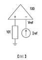
參考圖1的感測放大器電路作為實例。感測放大器100可連接到多個記憶體單元,其中每一記憶體單元能夠儲存二進制值。對於圖1的放大器電路的感測,單元101可輸出將要與參考電壓Vref或參考電流Iref比較的電壓或電流。放大器電路100可接著放大單元101的電壓輸出或電流輸出與參考電壓Vref或參考電流Iref之間的差以確定單元的資料是二進制0還是二進制1。Refer to the sense amplifier circuit of Figure 1 as an example. The
接下來,檢測二進制0讀取錯誤或二進制1讀取錯誤,且對二進制1讀取錯誤量和二進制0讀取錯誤量進行計數。一旦二進制1讀取錯誤量與二進制0讀取錯誤量之間的差已達到預定閾值,就可手動或自動地調整參考電壓Vref或參考電流Iref。可基於應用自動錯誤檢測技術以及熔絲技術來完成自動調整以調整參考電壓Vref或參考電流Iref。Next, a binary 0 reading error or a binary 1 reading error is detected, and the amount of binary 1 reading error and the amount of binary 0 reading error are counted. Once the difference between the binary 1 reading error amount and the binary 0 reading error amount has reached a predetermined threshold, the reference voltage Vref or the reference current Iref can be adjusted manually or automatically. The automatic adjustment can be completed based on the application of automatic error detection technology and fuse technology to adjust the reference voltage Vref or the reference current Iref.
記憶體裝置可以是例如電阻式隨機存取記憶體(RRAM),對於所述電阻式隨機存取記憶體,大多數讀取錯誤很可能是二進制1讀取錯誤。因此,如果計數器值已達到正預定數,那麼可調整寫入電壓或寫入時序以便提高所述電阻式隨機存取記憶體的循環耐久性。The memory device may be, for example, a resistive random access memory (RRAM). For the resistive random access memory, most read errors are likely to be binary 1 read errors. Therefore, if the counter value has reached a positive predetermined number, the write voltage or write timing can be adjusted to improve the cycle durability of the resistive random access memory.
另一實例中,可在一或多個所選記憶體塊的寫入操作期間使用一或多個錯誤計數器來實時記錄二進制1讀取錯誤量和/或二進制0讀取錯誤量。如果已確定計數器值高於正預定數,則可手動或自動地調整寫入電壓和/或時序以提高寫入操作的準確性。In another example, one or more error counters may be used during the write operation of one or more selected memory blocks to record the binary 1 read error amount and/or the binary 0 read error amount in real time. If it is determined that the counter value is higher than a positive predetermined number, the writing voltage and/or timing can be adjusted manually or automatically to improve the accuracy of the writing operation.
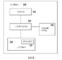
圖2繪示記憶體裝置200的硬體方塊圖。記憶體裝置200可包含電連接到連接介面210、記憶體陣列230、錯誤計數器231以及熔絲燒斷控制器240的記憶體控制電路220。連接介面210配置接收命令和/或資料或將所述命令和/或資料發射到外部裝置。FIG. 2 shows a hardware block diagram of the memory device 200. The memory device 200 may include a
記憶體陣列230含有多個記憶庫(memory bank),因為記憶庫中的每一個可含有用於儲存二進制資訊的多個記憶體單元。可在寫入操作期間使用錯誤計數器231來記錄二進制1讀取錯誤量與二進制0讀取錯誤量之間的差。在一實施例中,錯誤計數器231僅可在寫入操作或讀取操作期間記錄二進制0讀取錯誤量或二進制1讀取錯誤量。錯誤計數器231只可記錄記憶體塊或記憶庫的一部分而不是整個記憶體塊或記憶庫。每一記憶體塊或記憶庫可對應於專用錯誤計數器。或者,錯誤計數器可由多個記憶體塊或記憶庫共用。The
熔絲燒斷控制器240配置成燒斷一或多個熔絲以便啟動替代性電路,以便取代或調整現有功能。具體來說,對於本公開的記憶體裝置200,熔絲燒斷控制器240可儲存與將要調整的記憶體裝置200的一或多個參數相關的設定。舉例來說,熔絲燒斷控制器240可儲存對應於參數的具體設定的二進制值,所述參數可以是例如參考電壓或參考電流的感測參考。參數還可以是寫入電壓、編程電壓、設定電壓、重置電壓、形成電壓或時序。此外,通過將記憶體控制電路220配置成自動調整儲存在熔絲燒斷控制器240內的二進制值,記憶體裝置200將能夠自動調整感測參考。The
記憶體控制電路200可電連接到錯誤計數器231、連接介面210以及記憶體陣列230。值得注意的是,儘管將錯誤計數器231繪示為記憶體陣列230的一部分,但錯誤計數器可替代性地為記憶體控制電路220的一部分。記憶體控制電路220可配置成通過連接介面210接收一或多個操作,其中所述操作中的每一個是命令、讀取操作或寫入操作。記憶體控制電路220可進一步配置成響應於對記憶體陣列230進行一或多個讀取操作或寫入操作而檢測讀取錯誤,所述讀取錯誤是二進制0讀取錯誤或二進制1讀取錯誤。The memory control circuit 200 can be electrically connected to the
記憶體控制電路220可進一步配置成通過響應於檢測到二進制1讀取錯誤而遞增計數器值且通過響應於檢測到二進制0讀取錯誤而使計數器值遞減1來更新錯誤計數器231。隨後,記憶體控制電路220可響應於計數器值已達到正預定閾值或負預定閾值而調整參數。根據示範性實施例,記憶體控制電路220可響應於錯誤計數器231的計數器值已達到預定閾值的絕對值而調整感測參考。The
基本上,錯誤計數器231通過響應於檢測到二進制1讀取錯誤而進行一個單位遞增且通過響應於檢測到二進制0讀取錯誤而進行一個單位遞減來記錄二進制1讀取錯誤量與二進制0讀取錯誤量之間的差。Basically, the
在一實施例中,當記憶體控制電路220正對記憶體陣列進行讀取操作時,可使用內置裕度來進行讀取操作以便允許傳送位元具有良好裕度。In one embodiment, when the
記憶體控制電路220可配置成通過以下操作來調整感測參考:將計數器值重置到零;對多個記憶體單元進行讀取操作;累積二進制1讀取錯誤量和二進制0讀取錯誤量;以及基於更高的那個讀取錯誤量來調整感測參考以便遞減二進制1讀取錯誤量或二進制0讀取錯誤量。記憶體控制電路220可進一步配置成反覆調整感測參考直到計數器值低於正預定閾值或高於負預定閾值為止。The
記憶體控制電路220可配置成通過在記憶體控制電路配置成調整參考電壓或參考電流之前應用預定資料模式和與所述預定資料模式相反的二進制來更新錯誤計數器。由於感測參考可隨溫度而變化,所以記憶體控制電路200可配置成在感測參考根據不同溫度來變化時在不同溫度下調整所述感測參考。The
可在記憶體裝置200仍在出廠狀態下正進行測試時進行以上所描述的參數的調整。或者,可在記憶體裝置200正進行接通電源操作、正進行斷電操作時或響應於接收到命令而進行參數的調整。還可在寫入操作期間進行參數的調整。在已調整參數之後,可將錯誤計數器231的計數器值重置到零。The parameters described above can be adjusted while the memory device 200 is still being tested in the factory state. Alternatively, the parameter can be adjusted while the memory device 200 is performing a power-on operation, a power-off operation, or in response to receiving a command. It is also possible to adjust the parameters during the write operation. After the parameters have been adjusted, the counter value of the
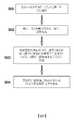
圖3繪示通過記憶體陣列230和記憶體控制電路220來進行以便產生二進制0讀取錯誤和二進制1讀取錯誤的功能的方塊圖。如圖3中所繪示,記憶體陣列的感測放大器(sense amplifier;SA)311可產生由錯誤校正碼(error correction code;ECC)電路313接收的50位元感測放大器輸出(sense amplifier output;SAOUT)312,所述錯誤校正碼電路例如實施例如博斯-喬赫裡-霍克文黑姆(Bose-Chaudhuri-Hocquenghem)譯碼的特定譯碼方案。ECC電路313可實施為記憶體控制電路220的一部分。ECC電路313接著將產生32位元經解碼感測放大器輸出 314和錯誤位置位元315,所述錯誤位置位元描述其中可能已出現讀取錯誤的每一位置。將經解碼感測放大器輸出314和錯誤位置位元315發送到並串轉換器316,所述並串轉換器將資料從並行格式轉換成串行格式以便以串行格式輸出經解碼感測放大器輸出 314和錯誤位置位元315。在這一實例中,假設已出現兩個錯誤317和錯誤318。第一錯誤317是其中讀取到二進制值0但實際值應該是1的二進制0讀取錯誤,且第二錯誤318是其中讀取到二進制值1但實際值應該是0的二進制1讀取錯誤。隨後將呈串行形式的錯誤位置位元315傳輸到錯誤計數器(例如錯誤計數器231)。FIG. 3 shows a block diagram of a function performed by the
錯誤計數器(例如錯誤計數器231)可以是例如圖4的4位元向上/向下錯誤計數器400。向上/向下錯誤計數器400能夠從0到15(也就是從0000到1111)進行計數。向上/向下錯誤計數器400的輸入端401將接收呈串行形式的錯誤位置位元315,且向上/向下錯誤計數器400將響應於接收到二進制1讀取錯誤而進行一個單位遞增(也就是使計數值遞增1)且將響應於接收到二進制0讀取錯誤而進行一個單位遞減(也就是使計數值遞減1)。將對照閾值使用向上/向下錯誤計數器400的4位元輸出Q0到輸出Q3以確定是否調整參數,所述參數例如記憶體裝置(例如記憶體裝置200)的感測參考(例如參考電壓Vref或參考電流Iref)。The error counter (for example, the error counter 231) may be, for example, the 4-bit up/down
圖5中繪示調整感測參考(例如參考電壓Vref或參考電流Iref)的概念。在圖5中,具有第一感測參考位準503的第一波形501是在高溫資料保持(high temperature data retention;HTDR)損失之前的對感測參考的應用的表徵。在已確定二進制1讀取錯誤量與二進制0讀取錯誤量之間的差已達到正預定閾值(這意味著與二進制0的讀數相比更多的二進制1的讀數是錯誤)之後,就將朝著二進制1調整感測參考以產生更多二進制0的讀數。因此,在HTDR損失之後,具有第二感測參考位準504的第二波形502變成對感測參考的應用的新的表徵。FIG. 5 illustrates the concept of adjusting the sensing reference (for example, the reference voltage Vref or the reference current Iref). In FIG. 5, the
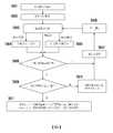
對於前述記憶體裝置(例如記憶體裝置200),本公開還提供一種如圖6的流程圖中所繪示的調整記憶體裝置的參數的方法。參考圖6,在步驟S601中,記憶體裝置將通過連接介面接收一或多個操作以對記憶體陣列進行所述操作,其中所述操作中的每一個是讀取操作或寫入操作。在步驟S602中,記憶體裝置將基於對記憶體陣列進行操作來檢測讀取錯誤,所述讀取錯誤是二進制0讀取錯誤或二進制1讀取錯誤。在步驟S603中,記憶體裝置將通過響應於二進制1讀取錯誤而遞增錯誤計數器的計數器值且響應於二進制0讀取錯誤而遞減所述計數器值來更新記憶體陣列的錯誤計數器。在步驟S604中,記憶體裝置將響應於計數器值已達到正預定閾值或負預定閾值而調整參數。For the aforementioned memory device (for example, the memory device 200), the present disclosure also provides a method for adjusting the parameters of the memory device as shown in the flowchart of FIG. 6. Referring to FIG. 6, in step S601, the memory device receives one or more operations through the connection interface to perform the operations on the memory array, wherein each of the operations is a read operation or a write operation. In step S602, the memory device will detect a read error based on operating the memory array, and the read error is a binary 0 read error or a binary 1 read error. In step S603, the memory device will update the error counter of the memory array by incrementing the counter value of the error counter in response to a binary 1 read error and decrementing the counter value in response to a binary 0 read error. In step S604, the memory device will adjust the parameter in response to the counter value having reached the positive or negative predetermined threshold.
所提供的調整記憶體裝置的參數的方法將基本上基於反映二進制0讀取錯誤量或二進制1讀取錯誤量的計數器值或二進制0讀取錯誤量與二進制1讀取錯誤量之間的差來調整一或多個關鍵參數。根據示範性實施例,在錯誤計數器已收集二進制0讀取錯誤與二進制1讀取錯誤之間的位錯誤的差之後,記憶體裝置將能夠確定後續調整的方向。如果二進制0讀取錯誤量達到二進制1讀取錯誤量的第一預定閾值,那麼可朝著二進制1自動調整感測參考直到二進制0讀取錯誤量與二進制1讀取錯誤量之間的差小於第二預定閾值為止。相反,如果二進制1讀取錯誤量達到二進制0讀取錯誤量的第三預定閾值,那麼可朝著二進制0自動調整感測參考直到二進制0讀取錯誤量與二進制1讀取錯誤量之間的差大於第四預定閾值為止。The provided method of adjusting the parameters of the memory device will basically be based on the counter value reflecting the binary 0 read error amount or the binary 1 read error amount or the difference between the binary 0 read error amount and the binary 1 read error amount To adjust one or more key parameters. According to an exemplary embodiment, after the error counter has collected the bit error difference between the binary 0 read error and the binary 1 read error, the memory device will be able to determine the direction of subsequent adjustment. If the binary 0 read error amount reaches the first predetermined threshold of the binary 1 read error amount, then the sensing reference can be automatically adjusted toward
可使用錯誤計數器來跟蹤來自全晶片單元陣列讀取或來自部分單元陣列讀取的錯誤位。可在接通電源操作期間、在讀取命令之後、在斷電操作之前、在從切斷電源操作恢復之後或通過獨立命令發生對感測參考的調整。可通過使用ECC或在不使用ECC的情況下完成對感測參考的調整。可通過例如調整儲存在熔絲燒斷控制器(例如熔絲燒斷控制器240)中的熔絲位以調整對應感測參考的設定來完成對感測參考的調整。在一實施例中,記憶體裝置可自動調整大於一個感測參考。Error counters can be used to track error bits from full wafer cell array reads or from partial cell array reads. The adjustment of the sensing reference can occur during a power-on operation, after a command is read, before a power-off operation, after recovery from a power-off operation, or through an independent command. The adjustment of the sensing reference can be done by using ECC or without using ECC. The adjustment of the sensing reference can be accomplished by, for example, adjusting the fuse position stored in the fuse blowing controller (such as the fuse blowing controller 240) to adjust the setting corresponding to the sensing reference. In one embodiment, the memory device can automatically adjust more than one sensing reference.
在出廠狀態下的測試程序期間,可根據預設定模式來測試整個記憶體塊。預設定模式可以是例如全一、全零、棋盤(checkboard)模式或棋盤模式的二進制反轉。接下來,可通過從儲存在記憶體塊中的預設定模式讀取來收集二進制0讀取錯誤和二進制1讀取錯誤(如果存在的話)。當記憶體裝置已出售給客戶時,調整記憶體裝置的參數的方法可在記憶體裝置正進行通電程序、正進行斷電程序時進行,或響應於接收到命令而進行。During the test procedure in the factory state, the entire memory block can be tested according to the preset mode. The preset mode may be, for example, all ones, all zeros, a checkboard mode, or a binary inversion of the checkboard mode. Next, binary 0 read errors and binary 1 read errors (if any) can be collected by reading from the preset pattern stored in the memory block. When the memory device has been sold to customers, the method of adjusting the parameters of the memory device may be performed while the memory device is performing a power-on procedure, a power-off procedure, or in response to receiving a command.
可使用錯誤計數器來收集讀取錯誤且隨後可調整感測參考提高二進制0讀取錯誤與二進制1讀取錯誤之間的再平衡。可通過應用裕度來進行讀取程序,使得傳送位具有良好裕度。讀取程序可多次進行,直到感測參考穩定為止。An error counter can be used to collect read errors and then the sensing reference can be adjusted to increase the rebalance between binary 0 read errors and binary 1 read errors. The reading procedure can be performed by applying the margin, so that the transfer bit has a good margin. The reading procedure can be performed multiple times until the sensing reference is stable.
錯誤計數器通常將初始化到零且響應於接收到二進制0讀取錯誤和二進制1讀取錯誤而持續向上計數或向下計數。一旦錯誤計數器的計數值達到正預定閾值或負預定閾值,就將進行對參數的調整,且接著將錯誤計數器重置回到零。The error counter will generally be initialized to zero and continue to count up or down in response to receiving a binary 0 read error and a binary 1 read error. Once the count value of the error counter reaches a positive predetermined threshold or a negative predetermined threshold, adjustment of the parameter will be performed, and then the error counter will be reset back to zero.
舉例來說,如果已通過連接介面接收到寫入操作,那麼可響應於錯誤計數器的計數值達到正閾值或負閾值而調整感測參考,且接著在已調整感測參考之後將計數值重置回到零。可通過由熔絲燒斷控制器控制的熔絲來調整感測參考。熔斷燒斷控制器可儲存對應於感測參考的設定的值以便通過燒斷某些熔絲來改變感測參考。在一實施例中,寫入電壓和寫入時序也可以是將要基於本公開的上述計數技術來調整的參數。For example, if a write operation has been received through the connection interface, the sensing reference can be adjusted in response to the count value of the error counter reaching the positive or negative threshold, and then the count value is reset after the sensing reference has been adjusted Back to zero. The sensing reference can be adjusted by the fuse controlled by the fuse blowing controller. The blow controller may store a set value corresponding to the sensing reference in order to change the sensing reference by blowing certain fuses. In an embodiment, the write voltage and the write timing may also be parameters to be adjusted based on the above-mentioned counting technique of the present disclosure.
為進一步闡明如在圖6和其對應描述中所公開的概念,圖7到圖9公開調整記憶體裝置的參數的方法的各種示範性實施例。圖7繪示根據本公開的一個實施例的通過測試程序來調整感測參考的方法。在步驟S701中,記憶體裝置將使對錯誤計數器的計數器值d進行計數初始化為零。在步驟S702中,記憶體裝置將對記憶庫的地址進行讀取操作以確定是否已出現讀取錯誤。在步驟S703中,如果存在二進制“0”讀取錯誤,那麼錯誤計數器將進行一個單位遞減(d = d - 1)。在步驟S704中,如果存在二進制1讀取錯誤,那麼錯誤計數器將進行一個單位遞增(d = d + 1)。To further clarify the concepts as disclosed in FIG. 6 and its corresponding description, FIGS. 7 to 9 disclose various exemplary embodiments of methods for adjusting the parameters of the memory device. FIG. 7 illustrates a method for adjusting a sensing reference through a test program according to an embodiment of the present disclosure. In step S701, the memory device initializes the counter value d of the error counter to zero. In step S702, the memory device will read the address of the memory bank to determine whether a read error has occurred. In step S703, if there is a binary "0" reading error, the error counter will be decremented by one unit (d = d-1). In step S704, if there is a binary 1 reading error, the error counter will be incremented by one unit (d = d + 1).
如果不存在讀取錯誤,那麼記憶體裝置將確定所述地址是否是用於進行讀取操作的最後一個地址(步驟S705)。如果是,那麼過程將繼續進行到步驟S707;否則,將在步驟S706中對下一地址進行讀取操作,且過程將環回到步驟S702。在步驟S707中,記憶體裝置將確定計數器值d是否已達到預定閾值N或-N。如果d ≤ -N,那麼記憶體裝置將朝著二進制1值調整感測參考(步驟S708)。如果d ≥ N,那麼記憶體裝置將朝著二進制0值調整感測參考(步驟S709)。如果-N ≤ d ≤ N,那麼記憶體裝置將使感測參考保持在當前位準下(步驟S710)。If there is no read error, the memory device will determine whether the address is the last address used for the read operation (step S705). If it is, the process will continue to step S707; otherwise, the next address will be read in step S706, and the process will loop back to step S702. In step S707, the memory device will determine whether the counter value d has reached a predetermined threshold N or -N. If d ≤ -N, the memory device will adjust the sensing reference toward the binary 1 value (step S708). If d ≥ N, the memory device will adjust the sensing reference toward the binary zero value (step S709). If -N ≤ d ≤ N, the memory device will keep the sensing reference at the current level (step S710).
圖8繪示根據本公開的另一實施例的作為用戶操作的調整感測參考的方法。在步驟S801中,記憶體裝置將使對錯誤計數器的計數器值d進行計數初始化為零。在步驟S802中,記憶體裝置將對記憶庫的地址進行讀取操作以確定是否已出現讀取錯誤。在步驟S803中,如果存在二進制0讀取錯誤,那麼錯誤計數器將進行一個單位遞減(d = d -1)。在步驟S804中,如果存在二進制1讀取錯誤,那麼錯誤計數器將進行一個單位遞增(d = d + 1)。FIG. 8 illustrates a method for adjusting a sensing reference as a user operation according to another embodiment of the present disclosure. In step S801, the memory device initializes the counter value d of the error counter to zero. In step S802, the memory device will read the address of the memory bank to determine whether a read error has occurred. In step S803, if there is a binary 0 reading error, the error counter will be decremented by one unit (d = d -1). In step S804, if there is a binary 1 reading error, the error counter will be incremented by one unit (d = d + 1).
如果不存在讀取錯誤,那麼記憶體裝置將確定計數器值d的絕對值是否已達到預定閾值N(步驟S805)。如果是,那麼過程將繼續進行到步驟S807;否則,將在步驟S806中進行下一讀取操作,且過程將環回到步驟S802。在步驟S807中,如果d ≥ N,那麼記憶體裝置將朝著二進制0值調整感測參考。如果d ≤ -N,那麼記憶體裝置將朝著二進制1值調整感測參考。在步驟S808中,錯誤計數器的計數器值d將重置為零且過程從步驟S806進行。If there is no read error, the memory device will determine whether the absolute value of the counter value d has reached the predetermined threshold N (step S805). If so, the process will continue to step S807; otherwise, the next read operation will be performed in step S806, and the process will loop back to step S802. In step S807, if d ≥ N, the memory device will adjust the sensing reference toward the binary zero value. If d ≤ -N, then the memory device will adjust the sensing reference toward the binary 1 value. In step S808, the counter value d of the error counter is reset to zero and the process proceeds from step S806.
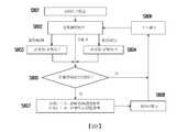
上述調整記憶體裝置的參數的方法將也可應用於調整寫入電壓和/或寫入時序以減少讀取錯誤,且在圖9中繪示這種方法的實施例。在步驟S901中,記憶體裝置將接收在記憶體位置中進行寫入操作的指令。在步驟S902中,記憶體裝置將使對錯誤計數器的計數器值d進行計數初始化為零。在步驟S903中,記憶體裝置將對記憶體位置進行讀取操作以確定是否已出現讀取錯誤。在一個實施例中,在進行讀取操作時將應用裕度。在步驟S904中,如果存在二進制0讀取錯誤,那麼計數器將進行一個單位遞減(d = d - 1)。在步驟S905中,如果存在二進制1讀取錯誤,那麼計數器將進行一個單位遞增(d = d + 1)。The method of adjusting the parameters of the memory device described above can also be applied to adjust the write voltage and/or write timing to reduce read errors, and an embodiment of this method is shown in FIG. 9. In step S901, the memory device will receive an instruction to perform a write operation in the memory location. In step S902, the memory device initializes the counter value d of the error counter to zero. In step S903, the memory device will perform a read operation on the memory location to determine whether a read error has occurred. In one embodiment, margins will be applied when performing read operations. In step S904, if there is a binary 0 reading error, the counter will be decremented by one unit (d = d-1). In step S905, if there is a binary 1 reading error, the counter will be incremented by one unit (d = d + 1).
如果不存在讀取錯誤,那麼記憶體裝置將確定計數器值d的絕對值是否已達到預定閾值N(步驟S906)。如果是,那麼過程將從步驟S909進行;否則,錯誤計數器的計數器值d將重置到零(步驟S907),接著將進行下一讀取操作(步驟S908)且過程將環回到步驟S903。在步驟S909中,記憶體裝置將確定感測參考是否已達到最大值或最小值。如果感測參考尚未達到最大值或最小值,那麼記憶體裝置將朝著二進制0值調整感測參考(如果d ≥ N)且朝著二進制1值調整感測參考(如果d ≤ -N)(步驟S910)。如果感測參考已達到最大值或最小值,那麼過程將從步驟S911進行。在步驟S911中,如果d > N,那麼將調整二進制1寫入電壓和時序條件,且如果d < -N,那麼將調整二進制0寫入電壓和時序條件。應注意,在這一實施例中,雖然無法進一步調整感測參考(也就是感測參考已達到最大值或最小值),但調整寫入電壓和時序條件(步驟S911)可有助於減少出現讀取錯誤的傾向。If there is no read error, the memory device will determine whether the absolute value of the counter value d has reached the predetermined threshold N (step S906). If so, the process will proceed from step S909; otherwise, the counter value d of the error counter will be reset to zero (step S907), then the next read operation will be performed (step S908) and the process will loop back to step S903. In step S909, the memory device will determine whether the sensing reference has reached the maximum value or the minimum value. If the sensing reference has not reached the maximum or minimum value, then the memory device will adjust the sensing reference towards the binary 0 value (if d ≥ N) and adjust the sensing reference towards the binary 1 value (if d ≤ -N) ( Step S910). If the sensing reference has reached the maximum value or the minimum value, the process will proceed from step S911. In step S911, if d>N, then the binary 1 write voltage and timing conditions will be adjusted, and if d<-N, then the binary 0 write voltage and timing conditions will be adjusted. It should be noted that in this embodiment, although the sensing reference cannot be further adjusted (that is, the sensing reference has reached the maximum or minimum value), adjusting the write voltage and timing conditions (step S911) can help reduce occurrences. The tendency to read errors.
鑒於前述描述,本公開適合於用於例如快閃記憶體、RRAM或其它類型的記憶體的記憶體裝置中,且可能夠通過調整感測參考的位準以提高良率且通過調整例如寫入電壓、形成電壓、設定電壓或重置電壓的參數以便優化寫入條件來在製造期間降低測試成本且提高良率。本公開還可通過使用熔絲技術以自動調整感測參考的位準以在客戶使用期間減少錯誤且調整例如寫入電壓、形成電壓、設定電壓或重置電壓的參數以便優化記憶體裝置的耐久性來提高客戶操作期間的可靠性。In view of the foregoing description, the present disclosure is suitable for use in memory devices such as flash memory, RRAM or other types of memory, and may be able to improve the yield by adjusting the level of the sensing reference and by adjusting, for example, writing Parameters of voltage, forming voltage, setting voltage, or reset voltage in order to optimize writing conditions to reduce test costs and increase yield during manufacturing. The present disclosure can also use fuse technology to automatically adjust the level of the sensing reference to reduce errors during customer use and adjust parameters such as write voltage, formation voltage, set voltage or reset voltage to optimize the durability of the memory device To improve reliability during customer operations.
雖然本發明已以實施例揭露如上,然其並非用以限定本發明,任何所屬技術領域中具有通常知識者,在不脫離本發明的精神和範圍內,當可作些許的更動與潤飾,故本發明的保護範圍當視後附的申請專利範圍所界定者為準。Although the present invention has been disclosed in the above embodiments, it is not intended to limit the present invention. Anyone with ordinary knowledge in the technical field can make some changes and modifications without departing from the spirit and scope of the present invention. The scope of protection of the present invention shall be determined by the scope of the attached patent application.
100、311:感測放大器101:單元200:記憶體裝置210:連接介面220:記憶體控制電路230:記憶體陣列231:錯誤計數器240:熔絲燒斷控制器312:感測放大器輸出313:錯誤校正碼電路314:經解碼感測放大器輸出315:錯誤位置位元316:並串轉換器317:第一錯誤318:第二錯誤400:向上/向下錯誤計數器401:輸入端501:第一波形502:第二波形503:第一感測參考位準504:第二感測參考位準Iref:參考電流Q0~Q3:輸出S601~S604、S701~S710、S801~S808、S901~S911:步驟Vref:參考電壓100, 311: sense amplifier101: unit200: Memory device210: connection interface220: Memory control circuit230: memory array231: Error counter240: Fuse blown controller312: Sense amplifier output313: error correction code circuit314: decoded sense amplifier output315: Wrong position bit316: Parallel to serial converter317: first error318: second error400: up/down error counter401: Input501: First Wave502: second waveform503: First sensing reference level504: Second sensing reference levelIref: reference currentQ0~Q3: outputS601~S604, S701~S710, S801~S808, S901~S911: stepsVref: reference voltage
圖1示出根據本公開的示範性實施例的感測放大器電壓參考和電流參考。 圖2繪示根據本公開的示範性實施例的記憶體裝置的硬體方塊圖。 圖3繪示根據本公開的示範性實施例的通過記憶體陣列和記憶體控制電路來進行的功能的方塊圖。 圖4繪示根據本公開的示範性實施例的錯誤計數器的電路圖。 圖5繪示根據本公開的示範性實施例的調整感測參考的概念。 圖6繪示根據本公開的示範性實施例的調整記憶體裝置的參數的方法。 圖7繪示根據本公開的示範性實施例的調整感測參考的方法。 圖8繪示根據本公開的示範性實施例的調整感測參考的方法。 圖9繪示根據本公開的示範性實施例的調整寫入電壓的方法。FIG. 1 shows a sense amplifier voltage reference and current reference according to an exemplary embodiment of the present disclosure. FIG. 2 illustrates a hardware block diagram of a memory device according to an exemplary embodiment of the present disclosure. FIG. 3 illustrates a block diagram of functions performed by a memory array and a memory control circuit according to an exemplary embodiment of the present disclosure. FIG. 4 is a circuit diagram of an error counter according to an exemplary embodiment of the present disclosure. FIG. 5 illustrates the concept of adjusting a sensing reference according to an exemplary embodiment of the present disclosure. FIG. 6 illustrates a method of adjusting parameters of a memory device according to an exemplary embodiment of the present disclosure. FIG. 7 illustrates a method of adjusting a sensing reference according to an exemplary embodiment of the present disclosure. FIG. 8 illustrates a method of adjusting a sensing reference according to an exemplary embodiment of the present disclosure. FIG. 9 illustrates a method of adjusting a write voltage according to an exemplary embodiment of the present disclosure.
200:記憶體裝置200: Memory device
210:連接介面210: connection interface
220:記憶體控制電路220: Memory control circuit
230:記憶體陣列230: memory array
231:錯誤計數器231: Error counter
240:熔絲燒斷控制器240: Fuse blown controller
Claims (20)
Translated fromChinesePriority Applications (1)
| Application Number | Priority Date | Filing Date | Title |
|---|---|---|---|
| TW109104132ATWI708248B (en) | 2020-02-11 | 2020-02-11 | Memory device and method of adjusting parameter used of memory device |
Applications Claiming Priority (1)
| Application Number | Priority Date | Filing Date | Title |
|---|---|---|---|
| TW109104132ATWI708248B (en) | 2020-02-11 | 2020-02-11 | Memory device and method of adjusting parameter used of memory device |
Publications (2)
| Publication Number | Publication Date |
|---|---|
| TWI708248Btrue TWI708248B (en) | 2020-10-21 |
| TW202131332A TW202131332A (en) | 2021-08-16 |
Family
ID=74091435
Family Applications (1)
| Application Number | Title | Priority Date | Filing Date |
|---|---|---|---|
| TW109104132ATWI708248B (en) | 2020-02-11 | 2020-02-11 | Memory device and method of adjusting parameter used of memory device |
Country Status (1)
| Country | Link |
|---|---|
| TW (1) | TWI708248B (en) |
Cited By (2)
| Publication number | Priority date | Publication date | Assignee | Title |
|---|---|---|---|---|
| TWI863197B (en)* | 2023-03-28 | 2024-11-21 | 華邦電子股份有限公司 | Semiconductor memory device, control method and control device |
| US12211547B2 (en) | 2023-01-09 | 2025-01-28 | Yangtze Memory Technologies Co., Ltd. | Dummy data-based read reference voltage search of NAND memory |
Citations (8)
| Publication number | Priority date | Publication date | Assignee | Title |
|---|---|---|---|---|
| TW432852B (en)* | 1998-02-20 | 2001-05-01 | Digital Video Express Lp | Information access control system and method |
| US7123049B2 (en)* | 2000-11-30 | 2006-10-17 | Renesas Technology Corporation | Output buffer circuit with control circuit for modifying supply voltage and transistor size |
| TW201115585A (en)* | 2009-06-30 | 2011-05-01 | Numonyx Bv | Bit error threshold and remapping a memory device |
| US8245087B2 (en)* | 2007-03-26 | 2012-08-14 | Cray Inc. | Multi-bit memory error management |
| US8499206B2 (en)* | 2010-03-04 | 2013-07-30 | Samsung Electronics Co., Ltd. | Memory system and method for preventing system hang |
| US20170192843A1 (en)* | 2014-08-08 | 2017-07-06 | Hewlett Packard Enterprise Development Lp | Error counters on a memory device |
| CN107924705A (en)* | 2015-08-28 | 2018-04-17 | 英特尔公司 | Memory Device Error Checking and Clearing Mode and Error Transparency |
| CN109155146A (en)* | 2016-05-28 | 2019-01-04 | 超威半导体公司 | Prosthetic device after integral type encapsulation |
- 2020
- 2020-02-11TWTW109104132Apatent/TWI708248B/enactive
Patent Citations (8)
| Publication number | Priority date | Publication date | Assignee | Title |
|---|---|---|---|---|
| TW432852B (en)* | 1998-02-20 | 2001-05-01 | Digital Video Express Lp | Information access control system and method |
| US7123049B2 (en)* | 2000-11-30 | 2006-10-17 | Renesas Technology Corporation | Output buffer circuit with control circuit for modifying supply voltage and transistor size |
| US8245087B2 (en)* | 2007-03-26 | 2012-08-14 | Cray Inc. | Multi-bit memory error management |
| TW201115585A (en)* | 2009-06-30 | 2011-05-01 | Numonyx Bv | Bit error threshold and remapping a memory device |
| US8499206B2 (en)* | 2010-03-04 | 2013-07-30 | Samsung Electronics Co., Ltd. | Memory system and method for preventing system hang |
| US20170192843A1 (en)* | 2014-08-08 | 2017-07-06 | Hewlett Packard Enterprise Development Lp | Error counters on a memory device |
| CN107924705A (en)* | 2015-08-28 | 2018-04-17 | 英特尔公司 | Memory Device Error Checking and Clearing Mode and Error Transparency |
| CN109155146A (en)* | 2016-05-28 | 2019-01-04 | 超威半导体公司 | Prosthetic device after integral type encapsulation |
Cited By (3)
| Publication number | Priority date | Publication date | Assignee | Title |
|---|---|---|---|---|
| US12211547B2 (en) | 2023-01-09 | 2025-01-28 | Yangtze Memory Technologies Co., Ltd. | Dummy data-based read reference voltage search of NAND memory |
| TWI878963B (en)* | 2023-01-09 | 2025-04-01 | 大陸商長江存儲科技有限責任公司 | Dummy data-based read reference voltage search of nand memory |
| TWI863197B (en)* | 2023-03-28 | 2024-11-21 | 華邦電子股份有限公司 | Semiconductor memory device, control method and control device |
Also Published As
| Publication number | Publication date |
|---|---|
| TW202131332A (en) | 2021-08-16 |
Similar Documents
| Publication | Publication Date | Title |
|---|---|---|
| CN111381999B (en) | Error correction in row hammer mitigation and target row refresh | |
| CN102132354B (en) | Fast low-power read of data in flash memory | |
| CN1551244B (en) | Error correctable nonvolatile memory for page copy operation and method thereof | |
| JP4129170B2 (en) | Semiconductor memory device and memory data correction method for memory cell | |
| US10395754B2 (en) | Method for decoding bits in a solid state drive, and related solid state drive | |
| US11107518B2 (en) | Extending operating temperature of storage device | |
| TWI754369B (en) | Physical unclonable function code generation appratus and method thereof | |
| CN109872763B (en) | Memory system for improving reliability of memory and memory management method thereof | |
| TWI708248B (en) | Memory device and method of adjusting parameter used of memory device | |
| US10783973B1 (en) | Memory device having parameter adjusting mechanism and method of adjusting parameter by memory device | |
| TWI702601B (en) | Semiconductor memory device | |
| CN108630278B (en) | Storage device and storage method | |
| CN115620798A (en) | Apparatus, system, and method for forced error checking and clear read | |
| KR20170044347A (en) | Memory device and operating method for memory device | |
| KR20090036146A (en) | Number of allowable bit errors per sector in memory device | |
| JP4614689B2 (en) | Dynamic reference voltage calibration built into FeRAM | |
| CN102543211A (en) | Early detection of degradation in NAND flash memory | |
| JP2020030872A (en) | Memory write control device and non-volatile memory defect determination method | |
| CN113284533B (en) | Memory device and method of adjusting parameters for memory device | |
| US20170322842A1 (en) | Memory controller, memory system, and method of controlling memory controller | |
| US20210295914A1 (en) | Storage control device, storage device, and storage control method | |
| TWI863197B (en) | Semiconductor memory device, control method and control device | |
| TW202533028A (en) | Control circuit, operating method and non-transitory computer readable storage medium | |
| TWI755830B (en) | Reading method of memory | |
| CN118737216A (en) | Semiconductor storage device, control method and control device |