TWI706452B - Manufacturing method of gate structure and gate structure - Google Patents
Manufacturing method of gate structure and gate structureDownload PDFInfo
- Publication number
- TWI706452B TWI706452BTW108112768ATW108112768ATWI706452BTW I706452 BTWI706452 BTW I706452BTW 108112768 ATW108112768 ATW 108112768ATW 108112768 ATW108112768 ATW 108112768ATW I706452 BTWI706452 BTW I706452B
- Authority
- TW
- Taiwan
- Prior art keywords
- trench
- oxide layer
- gate structure
- layer
- gate
- Prior art date
Links
- 238000004519manufacturing processMethods0.000titleclaimsabstractdescription37
- 239000000758substrateSubstances0.000claimsabstractdescription35
- 238000000034methodMethods0.000claimsabstractdescription23
- 229910052581Si3N4Inorganic materials0.000claimsabstractdescription19
- 238000005530etchingMethods0.000claimsabstractdescription13
- 229910021420polycrystalline siliconInorganic materials0.000claimsdescription18
- 229920005591polysiliconPolymers0.000claimsdescription18
- -1silicon nitride compoundChemical class0.000claimsdescription17
- 238000005229chemical vapour depositionMethods0.000claimsdescription6
- 238000001459lithographyMethods0.000claimsdescription6
- 230000003647oxidationEffects0.000claimsdescription4
- 238000007254oxidation reactionMethods0.000claimsdescription4
- HQVNEWCFYHHQES-UHFFFAOYSA-Nsilicon nitrideChemical compoundN12[Si]34N5[Si]62N3[Si]51N64HQVNEWCFYHHQES-UHFFFAOYSA-N0.000abstractdescription3
- 238000000206photolithographyMethods0.000abstract1
- 239000004065semiconductorSubstances0.000description9
- 238000010586diagramMethods0.000description5
- 230000005669field effectEffects0.000description5
- 229910044991metal oxideInorganic materials0.000description5
- 150000004706metal oxidesChemical class0.000description5
- 230000000694effectsEffects0.000description3
- UMVBXBACMIOFDO-UHFFFAOYSA-N[N].[Si]Chemical compound[N].[Si]UMVBXBACMIOFDO-UHFFFAOYSA-N0.000description1
- 238000003486chemical etchingMethods0.000description1
- 150000001875compoundsChemical class0.000description1
- 238000001312dry etchingMethods0.000description1
- 239000000463materialSubstances0.000description1
- 238000001039wet etchingMethods0.000description1
Images


Classifications
- H—ELECTRICITY
- H01—ELECTRIC ELEMENTS
- H01L—SEMICONDUCTOR DEVICES NOT COVERED BY CLASS H10
- H01L21/00—Processes or apparatus adapted for the manufacture or treatment of semiconductor or solid state devices or of parts thereof
- H01L21/02—Manufacture or treatment of semiconductor devices or of parts thereof
- H01L21/04—Manufacture or treatment of semiconductor devices or of parts thereof the devices having potential barriers, e.g. a PN junction, depletion layer or carrier concentration layer
- H01L21/18—Manufacture or treatment of semiconductor devices or of parts thereof the devices having potential barriers, e.g. a PN junction, depletion layer or carrier concentration layer the devices having semiconductor bodies comprising elements of Group IV of the Periodic Table or AIIIBV compounds with or without impurities, e.g. doping materials
- H01L21/28—Manufacture of electrodes on semiconductor bodies using processes or apparatus not provided for in groups H01L21/20 - H01L21/268
- H01L21/28008—Making conductor-insulator-semiconductor electrodes
- H01L21/28017—Making conductor-insulator-semiconductor electrodes the insulator being formed after the semiconductor body, the semiconductor being silicon
- H01L21/28026—Making conductor-insulator-semiconductor electrodes the insulator being formed after the semiconductor body, the semiconductor being silicon characterised by the conductor
- H01L21/28123—Lithography-related aspects, e.g. sub-lithography lengths; Isolation-related aspects, e.g. to solve problems arising at the crossing with the side of the device isolation; Planarisation aspects
- H—ELECTRICITY
- H01—ELECTRIC ELEMENTS
- H01L—SEMICONDUCTOR DEVICES NOT COVERED BY CLASS H10
- H01L21/00—Processes or apparatus adapted for the manufacture or treatment of semiconductor or solid state devices or of parts thereof
- H01L21/02—Manufacture or treatment of semiconductor devices or of parts thereof
- H01L21/04—Manufacture or treatment of semiconductor devices or of parts thereof the devices having potential barriers, e.g. a PN junction, depletion layer or carrier concentration layer
- H01L21/18—Manufacture or treatment of semiconductor devices or of parts thereof the devices having potential barriers, e.g. a PN junction, depletion layer or carrier concentration layer the devices having semiconductor bodies comprising elements of Group IV of the Periodic Table or AIIIBV compounds with or without impurities, e.g. doping materials
- H01L21/28—Manufacture of electrodes on semiconductor bodies using processes or apparatus not provided for in groups H01L21/20 - H01L21/268
- H01L21/28008—Making conductor-insulator-semiconductor electrodes
- H01L21/28017—Making conductor-insulator-semiconductor electrodes the insulator being formed after the semiconductor body, the semiconductor being silicon
- H01L21/28026—Making conductor-insulator-semiconductor electrodes the insulator being formed after the semiconductor body, the semiconductor being silicon characterised by the conductor
- H01L21/28114—Making conductor-insulator-semiconductor electrodes the insulator being formed after the semiconductor body, the semiconductor being silicon characterised by the conductor characterised by the sectional shape, e.g. T, inverted-T
- H—ELECTRICITY
- H10—SEMICONDUCTOR DEVICES; ELECTRIC SOLID-STATE DEVICES NOT OTHERWISE PROVIDED FOR
- H10D—INORGANIC ELECTRIC SEMICONDUCTOR DEVICES
- H10D30/00—Field-effect transistors [FET]
- H10D30/01—Manufacture or treatment
- H10D30/021—Manufacture or treatment of FETs having insulated gates [IGFET]
- H10D30/028—Manufacture or treatment of FETs having insulated gates [IGFET] of double-diffused metal oxide semiconductor [DMOS] FETs
- H10D30/0291—Manufacture or treatment of FETs having insulated gates [IGFET] of double-diffused metal oxide semiconductor [DMOS] FETs of vertical DMOS [VDMOS] FETs
- H10D30/0297—Manufacture or treatment of FETs having insulated gates [IGFET] of double-diffused metal oxide semiconductor [DMOS] FETs of vertical DMOS [VDMOS] FETs using recessing of the gate electrodes, e.g. to form trench gate electrodes
- H—ELECTRICITY
- H10—SEMICONDUCTOR DEVICES; ELECTRIC SOLID-STATE DEVICES NOT OTHERWISE PROVIDED FOR
- H10D—INORGANIC ELECTRIC SEMICONDUCTOR DEVICES
- H10D30/00—Field-effect transistors [FET]
- H10D30/60—Insulated-gate field-effect transistors [IGFET]
- H10D30/64—Double-diffused metal-oxide semiconductor [DMOS] FETs
- H10D30/66—Vertical DMOS [VDMOS] FETs
- H10D30/668—Vertical DMOS [VDMOS] FETs having trench gate electrodes, e.g. UMOS transistors
- H—ELECTRICITY
- H10—SEMICONDUCTOR DEVICES; ELECTRIC SOLID-STATE DEVICES NOT OTHERWISE PROVIDED FOR
- H10D—INORGANIC ELECTRIC SEMICONDUCTOR DEVICES
- H10D64/00—Electrodes of devices having potential barriers
- H10D64/01—Manufacture or treatment
- H—ELECTRICITY
- H10—SEMICONDUCTOR DEVICES; ELECTRIC SOLID-STATE DEVICES NOT OTHERWISE PROVIDED FOR
- H10D—INORGANIC ELECTRIC SEMICONDUCTOR DEVICES
- H10D64/00—Electrodes of devices having potential barriers
- H10D64/20—Electrodes characterised by their shapes, relative sizes or dispositions
- H10D64/27—Electrodes not carrying the current to be rectified, amplified, oscillated or switched, e.g. gates
- H10D64/311—Gate electrodes for field-effect devices
- H10D64/411—Gate electrodes for field-effect devices for FETs
- H10D64/511—Gate electrodes for field-effect devices for FETs for IGFETs
- H10D64/512—Disposition of the gate electrodes, e.g. buried gates
- H10D64/513—Disposition of the gate electrodes, e.g. buried gates within recesses in the substrate, e.g. trench gates, groove gates or buried gates
- H—ELECTRICITY
- H10—SEMICONDUCTOR DEVICES; ELECTRIC SOLID-STATE DEVICES NOT OTHERWISE PROVIDED FOR
- H10D—INORGANIC ELECTRIC SEMICONDUCTOR DEVICES
- H10D64/00—Electrodes of devices having potential barriers
- H10D64/20—Electrodes characterised by their shapes, relative sizes or dispositions
- H10D64/27—Electrodes not carrying the current to be rectified, amplified, oscillated or switched, e.g. gates
- H10D64/311—Gate electrodes for field-effect devices
- H10D64/411—Gate electrodes for field-effect devices for FETs
- H10D64/511—Gate electrodes for field-effect devices for FETs for IGFETs
- H10D64/514—Gate electrodes for field-effect devices for FETs for IGFETs characterised by the insulating layers
- H10D64/516—Gate electrodes for field-effect devices for FETs for IGFETs characterised by the insulating layers the thicknesses being non-uniform
- H—ELECTRICITY
- H10—SEMICONDUCTOR DEVICES; ELECTRIC SOLID-STATE DEVICES NOT OTHERWISE PROVIDED FOR
- H10D—INORGANIC ELECTRIC SEMICONDUCTOR DEVICES
- H10D84/00—Integrated devices formed in or on semiconductor substrates that comprise only semiconducting layers, e.g. on Si wafers or on GaAs-on-Si wafers
- H10D84/01—Manufacture or treatment
- H10D84/0123—Integrating together multiple components covered by H10D12/00 or H10D30/00, e.g. integrating multiple IGBTs
- H10D84/0126—Integrating together multiple components covered by H10D12/00 or H10D30/00, e.g. integrating multiple IGBTs the components including insulated gates, e.g. IGFETs
- H10D84/0135—Manufacturing their gate conductors
- H—ELECTRICITY
- H10—SEMICONDUCTOR DEVICES; ELECTRIC SOLID-STATE DEVICES NOT OTHERWISE PROVIDED FOR
- H10D—INORGANIC ELECTRIC SEMICONDUCTOR DEVICES
- H10D84/00—Integrated devices formed in or on semiconductor substrates that comprise only semiconducting layers, e.g. on Si wafers or on GaAs-on-Si wafers
- H10D84/01—Manufacture or treatment
- H10D84/02—Manufacture or treatment characterised by using material-based technologies
- H10D84/03—Manufacture or treatment characterised by using material-based technologies using Group IV technology, e.g. silicon technology or silicon-carbide [SiC] technology
- H10D84/038—Manufacture or treatment characterised by using material-based technologies using Group IV technology, e.g. silicon technology or silicon-carbide [SiC] technology using silicon technology, e.g. SiGe
Landscapes
- Engineering & Computer Science (AREA)
- Physics & Mathematics (AREA)
- Condensed Matter Physics & Semiconductors (AREA)
- General Physics & Mathematics (AREA)
- Manufacturing & Machinery (AREA)
- Computer Hardware Design (AREA)
- Microelectronics & Electronic Packaging (AREA)
- Power Engineering (AREA)
- Insulated Gate Type Field-Effect Transistor (AREA)
- Electrodes Of Semiconductors (AREA)
Abstract
Description
Translated fromChinese本案係關於一種閘結構之製造方法,尤指一種適用於半導體元件的閘結構之製造方法及閘結構。This case is about a manufacturing method of a gate structure, especially a manufacturing method and a gate structure suitable for a semiconductor device.
隨著科技的發展,金氧半場效電晶體(Metal Oxide Semiconductor Field Effect Transistor, MOSFET)已成為積體電路中常見的半導體元件,其中又以溝渠式金氧半場效電晶體(Trench MOSFET)具有較佳的特性,而逐漸取代傳統的金氧半場效電晶體。With the development of science and technology, Metal Oxide Semiconductor Field Effect Transistor (MOSFET) has become a common semiconductor component in integrated circuits. Among them, the trench metal oxide field effect transistor (Trench MOSFET) has more advantages. Excellent characteristics, and gradually replace the traditional metal oxide half field effect transistor.
一般而言,於溝渠式金氧半場效電晶體當中,係將閘極設置於半導體基材表面之溝渠中,以縮小閘極在半導體基材表面所佔據之面積,藉此可提升元件密度,其中閘極結構的一種實施態樣係為梯形閘極(Step gate),即為呈階梯狀的閘極結構。Generally speaking, in trench-type metal oxide half field effect transistors, the gate is arranged in the trench on the surface of the semiconductor substrate to reduce the area occupied by the gate on the surface of the semiconductor substrate, thereby increasing the device density. One implementation aspect of the gate structure is a step gate, which is a step gate structure.
在傳統的梯形閘極之製程中,需要進行兩次溝渠蝕刻之步驟,其係於第一次溝渠蝕刻後,透過沉積化合物以保護溝渠之側壁,之後再進行第二次溝渠蝕刻,進而形成呈階梯狀的閘極結構。然此製作流程較為繁瑣,且生產成本高。In the traditional trapezoidal gate manufacturing process, two trench etching steps are required. After the first trench etching, a compound is deposited to protect the sidewalls of the trench, and then the second trench etching is performed to form a pattern. Stepped gate structure. However, the production process is cumbersome and the production cost is high.
故此,如何發展一種有別於往的閘結構之製造方法及閘結構,以改善習知技術中的問題與缺點,實為目前技術領域中的重點課題。Therefore, how to develop a manufacturing method and a gate structure that are different from the conventional gate structure to improve the problems and shortcomings of the conventional technology is actually a key subject in the current technical field.
本案之目的為提供一種閘結構之製造方法及閘結構,俾解決並改善前述先前技術之問題與缺點。The purpose of this case is to provide a method for manufacturing a gate structure and a gate structure to solve and improve the problems and shortcomings of the aforementioned prior art.
本案之另一目的為提供一種閘結構之製造方法及閘結構,透過移除部分之底氧化層,使得在製造過程中僅需進行一次溝渠蝕刻,即可形成階梯狀之閘結構,進而達到簡化閘結構之製程及降低生產成本之功效。Another purpose of the present case is to provide a method for manufacturing a gate structure and a gate structure. By removing part of the bottom oxide layer, only one trench etching is required in the manufacturing process to form a stepped gate structure, thereby simplifying The manufacturing process of the gate structure and the effect of reducing production costs.
本案之另一目的為一種閘結構之製造方法及閘結構,藉由形成氮矽化合物層以保護底氧化層,並移除部分之底氧化層,而後再進一步形成閘氧化層,藉此可透過簡易製程形成適用於半導體元件之梯形閘結構。Another objective of this project is a method for manufacturing a gate structure and a gate structure. A silicon nitride compound layer is formed to protect the bottom oxide layer, and part of the bottom oxide layer is removed, and then a gate oxide layer is further formed so as to be transparent The simple process forms a trapezoidal gate structure suitable for semiconductor devices.
為達上述目的,本案之一較佳實施態樣為提供一種閘結構之製造方法,包括步驟:(a) 形成一遮罩氧化層於一基材,對該遮罩氧化層及該基材進行微影製程以形成一溝渠,並蝕刻該溝渠;(b) 移除該遮罩氧化層;(c) 形成一底氧化層於該基材之一表面以及該溝渠之一溝渠表面;(d) 形成一氮矽化合物層於該溝渠;(e) 移除部分之該底氧化層;(f) 移除該氮矽化合物層;(g) 形成一閘氧化層於該表面以及部分之該溝渠表面;以及(h) 形成一多晶矽層於該溝渠。In order to achieve the above-mentioned objective, a preferred embodiment of the present application is to provide a method for manufacturing a gate structure, which includes the steps of: (a) forming a mask oxide layer on a substrate, and performing processing on the mask oxide layer and the substrate Lithography process to form a trench and etch the trench; (b) remove the mask oxide layer; (c) form a bottom oxide layer on a surface of the substrate and a trench surface of the trench; (d) Forming a silicon nitride compound layer on the trench; (e) removing part of the bottom oxide layer; (f) removing the silicon nitride compound layer; (g) forming a gate oxide layer on the surface and part of the trench surface ; And (h) forming a polysilicon layer in the trench.
為達上述目的,本案之另一較佳實施態樣為提供一種閘結構,包括一基材、一底氧化層、一閘氧化層以及一多晶矽層。基材具有一表面,且該基材上形成有一溝渠,其中該溝渠具有一溝渠表面。底氧化層係設置於該溝渠表面之下端。閘氧化層係設置於該表面及該溝渠表面之上端,其中該閘氧化層之厚度係小於該底氧化層之厚度。多晶矽層係設置於該溝渠內,且係設置於該底氧化層並與該閘氧化層相連接。In order to achieve the above objective, another preferred embodiment of the present application is to provide a gate structure including a substrate, a bottom oxide layer, a gate oxide layer and a polysilicon layer. The substrate has a surface, and a trench is formed on the substrate, wherein the trench has a trench surface. The bottom oxide layer is arranged at the lower end of the trench surface. The gate oxide layer is arranged on the surface and the upper end of the trench surface, wherein the thickness of the gate oxide layer is smaller than the thickness of the bottom oxide layer. The polysilicon layer is arranged in the trench, and is arranged on the bottom oxide layer and connected with the gate oxide layer.
體現本案特徵與優點的一些典型實施例將在後段的說明中詳細敘述。應理解的是本案能夠在不同的態樣上具有各種的變化,其皆不脫離本案的範圍,且其中的說明及圖示在本質上係當作說明之用,而非架構於限制本案。Some typical embodiments embodying the features and advantages of this case will be described in detail in the following description. It should be understood that the case can have various changes in different aspects, which do not depart from the scope of the case, and the descriptions and diagrams therein are essentially for illustrative purposes, rather than being constructed to limit the case.
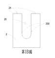
請參閱第1A圖至第1H圖,其係為本案較佳實施例之閘結構之製造方法之流程結構示意圖。如第1A圖至第1H圖所示,本案較佳實施例之閘結構之製造方法,係包括步驟如下:首先,形成遮罩氧化層1於基材2,且對遮罩氧化層1及基材2進行微影製程以形成溝渠20,並蝕刻溝渠20,以形成如第1A圖所示之結構。其次,移除遮罩氧化層1,以形成如第1B圖所示之結構。然後,形成底氧化層3於基材2之表面21以及溝渠20之溝渠表面200,以形成如第1C圖所示之結構。接著,形成氮矽化合物層4於溝渠20,以形成如第1D圖所示之結構。然後,移除部分之底氧化層3,以形成如第1E圖所示之結構。接著,移除氮矽化合物層4,以形成如第1F圖所示之結構。然後,形成閘氧化層5於基材2之表面21以及部分之溝渠表面200,以形成如第1G圖所示之結構。最後,形成多晶矽層6於溝渠20,最終形成如第1H圖所示之閘結構。Please refer to FIG. 1A to FIG. 1H, which are schematic diagrams of the flow structure of the method of manufacturing the gate structure of the preferred embodiment of the present invention. As shown in Fig. 1A to Fig. 1H, the manufacturing method of the gate structure of the preferred embodiment of this case includes the following steps: firstly, a
換言之,本案提供之閘結構之製造方法,係透過移除部分之底氧化層,使得在製造過程中僅需進行一次溝渠蝕刻,即可形成階梯狀之閘結構,進而達到簡化閘結構之製程及降低生產成本之功效。In other words, the manufacturing method of the gate structure provided in this case is by removing part of the bottom oxide layer, so that only one trench etching is required in the manufacturing process to form a stepped gate structure, thereby simplifying the manufacturing process of the gate structure and The effect of reducing production costs.
於一些實施例中,在形成遮罩氧化層1於基材2,對遮罩氧化層1及基材2進行微影製程以形成溝渠20,並蝕刻溝渠20之步驟中,係可進一步包括步驟:首先,透過化學氣相沉積法以形成遮罩氧化層1於基材2。其次,對遮罩氧化層1及基材2進行溝渠圖形佈建及微影製程,以形成溝渠20。然後,對遮罩氧化層1進行蝕刻,例如濕蝕刻或化學蝕刻等。最後,對溝渠20進行蝕刻,例如乾蝕刻,以形成如第1A圖所示之結構。In some embodiments, in the step of forming the
於一些實施例中,在形成底氧化層3於基材2之表面21以及溝渠表面200之步驟中,係可包括透過熱氧化法以形成底氧化層3於表面21以及溝渠表面200,藉此以形成如第1C圖所示之結構,然並不以此為限。In some embodiments, the step of forming the
於一些實施例中,在形成氮矽化合物層4於溝渠20之步驟中,係可進一步包括步驟:首先,透過化學氣相沉積法以形成氮矽化合物層4於溝渠20內並填滿溝渠20,使氮矽化合物層4形成於底氧化層3上。接著,對氮矽化合物層4進行回蝕刻(Etch back)以去除部分之氮矽化合物層4,使得氮矽化合物層4的水平面與基材2之表面21齊平,以形成如第1D圖所示之結構。In some embodiments, the step of forming the
於一些實施例中,在移除部分之底氧化層3之步驟中,係移除位於溝渠表面200之上端之底氧化層3,以及移除位於表面21之底氧化層3,以形成如第1E圖所示之結構。其中,溝渠表面200之上端係指溝渠表面200當中較為接近表面21之一端,且移除後所剩餘之底氧化層3之高度H係接近但大於溝渠20之深度D之二分之一,即
於一些實施例中,在形成閘氧化層5於基材2之表面21以及部分之溝渠表面200之步驟中,係可包括透過熱氧化法以形成閘氧化層5於表面21以及部分之溝渠表面200,具體而言,係形成閘氧化層5於表面21以及溝渠表面200之上端,以形成如第1G圖所示之結構。亦即,係將閘氧化層5形成於因移除底氧化層3後所裸露出之表面21與溝渠表面200之上端,使得底氧化層3與閘氧化層5可共同地將表面21及溝渠表面200完全覆蓋,且其中所形成之閘氧化層5之厚度T1係小於底氧化層3之厚度T2。In some embodiments, the step of forming the
於一些實施例中,在形成多晶矽層6於溝渠20之步驟中,係包括步驟:首先,透過化學氣相沉積法以形成多晶矽層6於溝渠20並填滿溝渠20,使多晶矽層6形成於底氧化層3上且與閘氧化層5相連接。接著,對多晶矽層6進行回蝕刻以去除部分之多晶矽層6,使得多晶矽層6的水平面與基材2之表面21齊平,最終所形成之閘結構即為第1H圖所示之結構。In some embodiments, the step of forming the
易言之,本案提供之閘結構之製造方法,係藉由形成氮矽化合物層以保護底氧化層,並移除部分之底氧化層,而後再進一步形成閘氧化層,藉此可透過簡易製程形成適用於半導體元件之梯形閘結構。In other words, the manufacturing method of the gate structure provided in this case is to form a silicon nitride compound layer to protect the bottom oxide layer, remove part of the bottom oxide layer, and then further form the gate oxide layer, which can be achieved through a simple process Form a trapezoidal gate structure suitable for semiconductor devices.
請參閱第2圖,第2圖係顯示本案較佳實施例之閘結構之結構示意圖。如第2圖所示,本案較佳實施例之閘結構10係可透過如前述之閘結構之製造方法所形成,閘結構10係包括基材2、底氧化層3、閘氧化層5及多晶矽層6。其中,閘結構10係可適用於半導體元件,例如但不限於適用於溝渠式金氧半場效電晶體。Please refer to Figure 2. Figure 2 is a schematic diagram showing the structure of the gate structure of the preferred embodiment of the present invention. As shown in Figure 2, the
基材2具有表面21,且基材2上形成有溝渠20,其中溝渠20具有溝渠表面200。底氧化層3係設置於溝渠表面200之下端,閘氧化層5係設置於基材2之表面21及溝渠表面200之上端。其中,溝渠表面200之上端係指溝渠表面200當中較為接近基材2之表面21之一端,溝渠表面200之下端係指溝渠表面200當中較為接近溝渠20之底部之一端。並且,閘氧化層5之厚度T1係小於底氧化層3之厚度T2。多晶矽層6係設置於溝渠20內,且係設置於底氧化層3上並與閘氧化層5相連接。藉此,以構成體積小且具有較佳電氣特性之梯形閘結構。The
綜上所述,本案係提供一種閘結構之製造方法及閘結構,透過移除部分之底氧化層,使得製造過程中僅需進行一次溝渠蝕刻,即可形成階梯狀之閘結構,進而達到簡化閘結構之製程及降低生產成本之功效。同時,藉由形成氮矽化合物層以保護底氧化層,並於移除部分之底氧化層後再進一步形成閘氧化層,藉此可透過簡易製程形成適用於半導體元件之梯形閘結構。To sum up, this case provides a gate structure manufacturing method and gate structure. By removing part of the bottom oxide layer, only one trench etching is required in the manufacturing process to form a stepped gate structure, thereby simplifying The manufacturing process of the gate structure and the effect of reducing production costs. At the same time, by forming a silicon nitride compound layer to protect the bottom oxide layer, and after removing part of the bottom oxide layer, a gate oxide layer is further formed, thereby forming a ladder gate structure suitable for semiconductor devices through a simple process.
縱使本發明已由上述之實施例詳細敘述而可由熟悉本技藝之人士任施匠思而為諸般修飾,然皆不脫如附申請專利範圍所欲保護者。Even though the present invention has been described in detail by the above-mentioned embodiments and can be modified in many ways by those skilled in the art, it does not deviate from the scope of the attached patent application.
1:遮罩氧化層1: Mask oxide layer
10:閘結構10: Gate structure
2:基材2: substrate
20:溝渠20: Ditch
200:溝渠表面200: Ditch surface
21:表面21: Surface
3:底氧化層3: bottom oxide layer
4:氮矽化合物層4: Nitrogen silicon compound layer
5:閘氧化層5: Gate oxide layer
6:多晶矽層6: Polysilicon layer
H:高度H: height
D:深度D: depth
T1、T2:厚度T1, T2: thickness
第1A圖至第1H圖係為本案較佳實施例之閘結構之製造方法之流程結構示意圖。 第2圖係顯示本案較佳實施例之閘結構之結構示意圖。Figures 1A to 1H are schematic diagrams of the flow structure of the manufacturing method of the gate structure of the preferred embodiment of the present invention. Figure 2 is a schematic diagram showing the structure of the gate structure of the preferred embodiment of the present invention.
10:閘結構10: Gate structure
2:基材2: substrate
20:溝渠20: Ditch
200:溝渠表面200: Ditch surface
21:表面21: Surface
3:底氧化層3: bottom oxide layer
5:閘氧化層5: Gate oxide layer
6:多晶矽層6: Polysilicon layer
T1、T2:厚度T1, T2: thickness
Claims (8)
Translated fromChinesePriority Applications (2)
| Application Number | Priority Date | Filing Date | Title |
|---|---|---|---|
| TW108112768ATWI706452B (en) | 2019-04-11 | 2019-04-11 | Manufacturing method of gate structure and gate structure |
| US16/547,828US11139172B2 (en) | 2019-04-11 | 2019-08-22 | Manufacturing method of gate structure |
Applications Claiming Priority (1)
| Application Number | Priority Date | Filing Date | Title |
|---|---|---|---|
| TW108112768ATWI706452B (en) | 2019-04-11 | 2019-04-11 | Manufacturing method of gate structure and gate structure |
Publications (2)
| Publication Number | Publication Date |
|---|---|
| TWI706452Btrue TWI706452B (en) | 2020-10-01 |
| TW202038314A TW202038314A (en) | 2020-10-16 |
Family
ID=72748163
Family Applications (1)
| Application Number | Title | Priority Date | Filing Date |
|---|---|---|---|
| TW108112768ATWI706452B (en) | 2019-04-11 | 2019-04-11 | Manufacturing method of gate structure and gate structure |
Country Status (2)
| Country | Link |
|---|---|
| US (1) | US11139172B2 (en) |
| TW (1) | TWI706452B (en) |
Families Citing this family (1)
| Publication number | Priority date | Publication date | Assignee | Title |
|---|---|---|---|---|
| US12439621B2 (en)* | 2021-06-07 | 2025-10-07 | Stmicroelectronics Pte Ltd | Method of making a charge coupled field effect rectifier diode |
Citations (3)
| Publication number | Priority date | Publication date | Assignee | Title |
|---|---|---|---|---|
| US6391699B1 (en)* | 2000-06-05 | 2002-05-21 | Fairchild Semiconductor Corporation | Method of manufacturing a trench MOSFET using selective growth epitaxy |
| US7371641B2 (en)* | 2004-10-29 | 2008-05-13 | International Rectifier Corporation | Method of making a trench MOSFET with deposited oxide |
| US20100187602A1 (en)* | 2009-01-29 | 2010-07-29 | Woolsey Debra S | Methods for making semiconductor devices using nitride consumption locos oxidation |
Family Cites Families (16)
| Publication number | Priority date | Publication date | Assignee | Title |
|---|---|---|---|---|
| TW567560B (en)* | 2002-07-02 | 2003-12-21 | Mosel Vitelic Inc | Method of forming bottom oxide layer in trench |
| US7652326B2 (en)* | 2003-05-20 | 2010-01-26 | Fairchild Semiconductor Corporation | Power semiconductor devices and methods of manufacture |
| JP2005085996A (en)* | 2003-09-09 | 2005-03-31 | Toshiba Corp | Semiconductor device and manufacturing method thereof |
| KR100556527B1 (en)* | 2004-11-04 | 2006-03-06 | 삼성전자주식회사 | Trench isolation layer formation method and nonvolatile memory device manufacturing method |
| KR100629356B1 (en)* | 2004-12-23 | 2006-09-29 | 삼성전자주식회사 | Flash memory device having pillar pattern and manufacturing method |
| US7315474B2 (en)* | 2005-01-03 | 2008-01-01 | Macronix International Co., Ltd | Non-volatile memory cells, memory arrays including the same and methods of operating cells and arrays |
| KR100829600B1 (en)* | 2006-10-02 | 2008-05-14 | 삼성전자주식회사 | Manufacturing method of nonvolatile memory device |
| US20080233709A1 (en)* | 2007-03-22 | 2008-09-25 | Infineon Technologies North America Corp. | Method for removing material from a semiconductor |
| JP5644242B2 (en)* | 2009-09-09 | 2014-12-24 | 大日本印刷株式会社 | Through electrode substrate and manufacturing method thereof |
| US8558305B2 (en)* | 2009-12-28 | 2013-10-15 | Stmicroelectronics S.R.L. | Method for manufacturing a power device being integrated on a semiconductor substrate, in particular having a field plate vertical structure and corresponding device |
| KR101755234B1 (en)* | 2010-08-26 | 2017-07-07 | 삼성전자 주식회사 | Method for fabricating non-volatile memory device |
| JP2012231007A (en)* | 2011-04-26 | 2012-11-22 | Elpida Memory Inc | Method of manufacturing semiconductor device |
| EP2942804B1 (en)* | 2014-05-08 | 2017-07-12 | Flosfia Inc. | Crystalline multilayer structure and semiconductor device |
| US9570360B2 (en)* | 2014-08-27 | 2017-02-14 | International Business Machines Corporation | Dual channel material for finFET for high performance CMOS |
| US10566242B2 (en)* | 2016-12-13 | 2020-02-18 | Taiwan Semiconductor Manufacturing Company, Ltd. | Minimization of plasma doping induced fin height loss |
| US10692988B2 (en)* | 2018-11-26 | 2020-06-23 | Infineon Technologies Austria Ag | Semiconductor device having integrated MOS-gated or Schottky diodes |
- 2019
- 2019-04-11TWTW108112768Apatent/TWI706452B/enactive
- 2019-08-22USUS16/547,828patent/US11139172B2/enactiveActive
Patent Citations (5)
| Publication number | Priority date | Publication date | Assignee | Title |
|---|---|---|---|---|
| US6391699B1 (en)* | 2000-06-05 | 2002-05-21 | Fairchild Semiconductor Corporation | Method of manufacturing a trench MOSFET using selective growth epitaxy |
| US6576954B2 (en)* | 2000-06-05 | 2003-06-10 | Fairchild Semiconductor Corporation | Trench MOSFET formed using selective epitaxial growth |
| US7371641B2 (en)* | 2004-10-29 | 2008-05-13 | International Rectifier Corporation | Method of making a trench MOSFET with deposited oxide |
| US8106446B2 (en)* | 2004-10-29 | 2012-01-31 | International Rectifier Corporation | Trench MOSFET with deposited oxide |
| US20100187602A1 (en)* | 2009-01-29 | 2010-07-29 | Woolsey Debra S | Methods for making semiconductor devices using nitride consumption locos oxidation |
Also Published As
| Publication number | Publication date |
|---|---|
| US11139172B2 (en) | 2021-10-05 |
| US20200328084A1 (en) | 2020-10-15 |
| TW202038314A (en) | 2020-10-16 |
Similar Documents
| Publication | Publication Date | Title |
|---|---|---|
| CN104733291A (en) | Method For Integrated Circuit Patterning | |
| CN104485286B (en) | MOSFET comprising middle pressure SGT structures and preparation method thereof | |
| US9748138B2 (en) | Metal layer end-cut flow | |
| TWI706452B (en) | Manufacturing method of gate structure and gate structure | |
| TWI739087B (en) | Manufacturing method of split gate structure and split gate structure | |
| CN101339902B (en) | high-voltage semiconductor device and method of fabricating semiconductor high-voltage device | |
| CN110867377B (en) | Planarization method of virtual gate | |
| CN114864479A (en) | Semiconductor device and method of making the same | |
| TWI715967B (en) | Semiconductor structure and method of processing the same | |
| US6958276B2 (en) | Method of manufacturing trench-type MOSFET | |
| CN109494187B (en) | Method for manufacturing semiconductor structure | |
| CN115394646B (en) | Semiconductor device and method for manufacturing the same | |
| TWI508222B (en) | Method for forming trenches and trench isolation on a substrate | |
| TWI704647B (en) | Integrated circuit and process thereof | |
| CN119383950B (en) | Method for forming semiconductor structure | |
| TWI532096B (en) | Process of forming slit in substrate | |
| CN102592993A (en) | Method for improving uniformity of chemical mechanical planarization process of back gate engineering metal plug | |
| CN111725137B (en) | Method for forming semiconductor device | |
| CN108847393B (en) | Method for forming fin field effect transistor structure | |
| KR100629691B1 (en) | Manufacturing Method of Semiconductor Device | |
| TW202339267A (en) | Trench power semiconductor device and manufactureing method thereof | |
| KR100674352B1 (en) | Manufacturing Method of Semiconductor Device | |
| KR20110037242A (en) | Method for forming semiconductor device | |
| CN100437938C (en) | Method for manufacturing conductive wire | |
| KR100427718B1 (en) | Method for manufacturing a semiconductor device |