TWI705868B - Wafer production method - Google Patents
Wafer production methodDownload PDFInfo
- Publication number
- TWI705868B TWI705868BTW106112631ATW106112631ATWI705868BTW I705868 BTWI705868 BTW I705868BTW 106112631 ATW106112631 ATW 106112631ATW 106112631 ATW106112631 ATW 106112631ATW I705868 BTWI705868 BTW I705868B
- Authority
- TW
- Taiwan
- Prior art keywords
- pulses
- gan
- laser beam
- laser
- pulse
- Prior art date
Links
- 238000004519manufacturing processMethods0.000titleclaimsabstractdescription8
- JMASRVWKEDWRBT-UHFFFAOYSA-NGallium nitrideChemical compound[Ga]#NJMASRVWKEDWRBT-UHFFFAOYSA-N0.000claimsabstractdescription76
- 235000012431wafersNutrition0.000claimsabstractdescription21
- 238000000034methodMethods0.000claimsdescription31
- 230000006378damageEffects0.000claimsdescription16
- 239000013078crystalSubstances0.000claimsdescription14
- 230000015572biosynthetic processEffects0.000claims1
- 230000001678irradiating effectEffects0.000abstractdescription6
- 229910002601GaNInorganic materials0.000description54
- 238000003384imaging methodMethods0.000description11
- 229910052733galliumInorganic materials0.000description3
- 238000010586diagramMethods0.000description2
- 230000003287optical effectEffects0.000description2
- 230000002093peripheral effectEffects0.000description2
- 239000000853adhesiveSubstances0.000description1
- 230000001070adhesive effectEffects0.000description1
- 230000000694effectsEffects0.000description1
- 239000003822epoxy resinSubstances0.000description1
- 239000011521glassSubstances0.000description1
- 239000000463materialSubstances0.000description1
- 239000000203mixtureSubstances0.000description1
- 238000005498polishingMethods0.000description1
- 229920000647polyepoxidePolymers0.000description1
- 229910052710siliconInorganic materials0.000description1
- 239000010703siliconSubstances0.000description1
- 238000001179sorption measurementMethods0.000description1
- SITVSCPRJNYAGV-UHFFFAOYSA-LtelluriteChemical compound[O-][Te]([O-])=OSITVSCPRJNYAGV-UHFFFAOYSA-L0.000description1
- 230000009466transformationEffects0.000description1
Images


Classifications
- H—ELECTRICITY
- H01—ELECTRIC ELEMENTS
- H01L—SEMICONDUCTOR DEVICES NOT COVERED BY CLASS H10
- H01L21/00—Processes or apparatus adapted for the manufacture or treatment of semiconductor or solid state devices or of parts thereof
- H01L21/70—Manufacture or treatment of devices consisting of a plurality of solid state components formed in or on a common substrate or of parts thereof; Manufacture of integrated circuit devices or of parts thereof
- H01L21/77—Manufacture or treatment of devices consisting of a plurality of solid state components or integrated circuits formed in, or on, a common substrate
- H01L21/78—Manufacture or treatment of devices consisting of a plurality of solid state components or integrated circuits formed in, or on, a common substrate with subsequent division of the substrate into plural individual devices
- B—PERFORMING OPERATIONS; TRANSPORTING
- B23—MACHINE TOOLS; METAL-WORKING NOT OTHERWISE PROVIDED FOR
- B23K—SOLDERING OR UNSOLDERING; WELDING; CLADDING OR PLATING BY SOLDERING OR WELDING; CUTTING BY APPLYING HEAT LOCALLY, e.g. FLAME CUTTING; WORKING BY LASER BEAM
- B23K26/00—Working by laser beam, e.g. welding, cutting or boring
- B23K26/0006—Working by laser beam, e.g. welding, cutting or boring taking account of the properties of the material involved
- B—PERFORMING OPERATIONS; TRANSPORTING
- B23—MACHINE TOOLS; METAL-WORKING NOT OTHERWISE PROVIDED FOR
- B23K—SOLDERING OR UNSOLDERING; WELDING; CLADDING OR PLATING BY SOLDERING OR WELDING; CUTTING BY APPLYING HEAT LOCALLY, e.g. FLAME CUTTING; WORKING BY LASER BEAM
- B23K26/00—Working by laser beam, e.g. welding, cutting or boring
- B23K26/02—Positioning or observing the workpiece, e.g. with respect to the point of impact; Aligning, aiming or focusing the laser beam
- B23K26/03—Observing, e.g. monitoring, the workpiece
- B23K26/032—Observing, e.g. monitoring, the workpiece using optical means
- B—PERFORMING OPERATIONS; TRANSPORTING
- B23—MACHINE TOOLS; METAL-WORKING NOT OTHERWISE PROVIDED FOR
- B23K—SOLDERING OR UNSOLDERING; WELDING; CLADDING OR PLATING BY SOLDERING OR WELDING; CUTTING BY APPLYING HEAT LOCALLY, e.g. FLAME CUTTING; WORKING BY LASER BEAM
- B23K26/00—Working by laser beam, e.g. welding, cutting or boring
- B23K26/02—Positioning or observing the workpiece, e.g. with respect to the point of impact; Aligning, aiming or focusing the laser beam
- B23K26/035—Aligning the laser beam
- B—PERFORMING OPERATIONS; TRANSPORTING
- B23—MACHINE TOOLS; METAL-WORKING NOT OTHERWISE PROVIDED FOR
- B23K—SOLDERING OR UNSOLDERING; WELDING; CLADDING OR PLATING BY SOLDERING OR WELDING; CUTTING BY APPLYING HEAT LOCALLY, e.g. FLAME CUTTING; WORKING BY LASER BEAM
- B23K26/00—Working by laser beam, e.g. welding, cutting or boring
- B23K26/02—Positioning or observing the workpiece, e.g. with respect to the point of impact; Aligning, aiming or focusing the laser beam
- B23K26/06—Shaping the laser beam, e.g. by masks or multi-focusing
- B23K26/062—Shaping the laser beam, e.g. by masks or multi-focusing by direct control of the laser beam
- B23K26/0622—Shaping the laser beam, e.g. by masks or multi-focusing by direct control of the laser beam by shaping pulses
- B—PERFORMING OPERATIONS; TRANSPORTING
- B23—MACHINE TOOLS; METAL-WORKING NOT OTHERWISE PROVIDED FOR
- B23K—SOLDERING OR UNSOLDERING; WELDING; CLADDING OR PLATING BY SOLDERING OR WELDING; CUTTING BY APPLYING HEAT LOCALLY, e.g. FLAME CUTTING; WORKING BY LASER BEAM
- B23K26/00—Working by laser beam, e.g. welding, cutting or boring
- B23K26/08—Devices involving relative movement between laser beam and workpiece
- B23K26/0823—Devices involving rotation of the workpiece
- B—PERFORMING OPERATIONS; TRANSPORTING
- B23—MACHINE TOOLS; METAL-WORKING NOT OTHERWISE PROVIDED FOR
- B23K—SOLDERING OR UNSOLDERING; WELDING; CLADDING OR PLATING BY SOLDERING OR WELDING; CUTTING BY APPLYING HEAT LOCALLY, e.g. FLAME CUTTING; WORKING BY LASER BEAM
- B23K26/00—Working by laser beam, e.g. welding, cutting or boring
- B23K26/08—Devices involving relative movement between laser beam and workpiece
- B23K26/083—Devices involving movement of the workpiece in at least one axial direction
- B23K26/0853—Devices involving movement of the workpiece in at least in two axial directions, e.g. in a plane
- B—PERFORMING OPERATIONS; TRANSPORTING
- B23—MACHINE TOOLS; METAL-WORKING NOT OTHERWISE PROVIDED FOR
- B23K—SOLDERING OR UNSOLDERING; WELDING; CLADDING OR PLATING BY SOLDERING OR WELDING; CUTTING BY APPLYING HEAT LOCALLY, e.g. FLAME CUTTING; WORKING BY LASER BEAM
- B23K26/00—Working by laser beam, e.g. welding, cutting or boring
- B23K26/08—Devices involving relative movement between laser beam and workpiece
- B23K26/10—Devices involving relative movement between laser beam and workpiece using a fixed support, i.e. involving moving the laser beam
- B—PERFORMING OPERATIONS; TRANSPORTING
- B23—MACHINE TOOLS; METAL-WORKING NOT OTHERWISE PROVIDED FOR
- B23K—SOLDERING OR UNSOLDERING; WELDING; CLADDING OR PLATING BY SOLDERING OR WELDING; CUTTING BY APPLYING HEAT LOCALLY, e.g. FLAME CUTTING; WORKING BY LASER BEAM
- B23K26/00—Working by laser beam, e.g. welding, cutting or boring
- B23K26/36—Removing material
- B23K26/362—Laser etching
- B23K26/364—Laser etching for making a groove or trench, e.g. for scribing a break initiation groove
- B—PERFORMING OPERATIONS; TRANSPORTING
- B23—MACHINE TOOLS; METAL-WORKING NOT OTHERWISE PROVIDED FOR
- B23K—SOLDERING OR UNSOLDERING; WELDING; CLADDING OR PLATING BY SOLDERING OR WELDING; CUTTING BY APPLYING HEAT LOCALLY, e.g. FLAME CUTTING; WORKING BY LASER BEAM
- B23K26/00—Working by laser beam, e.g. welding, cutting or boring
- B23K26/36—Removing material
- B23K26/38—Removing material by boring or cutting
- B—PERFORMING OPERATIONS; TRANSPORTING
- B23—MACHINE TOOLS; METAL-WORKING NOT OTHERWISE PROVIDED FOR
- B23K—SOLDERING OR UNSOLDERING; WELDING; CLADDING OR PLATING BY SOLDERING OR WELDING; CUTTING BY APPLYING HEAT LOCALLY, e.g. FLAME CUTTING; WORKING BY LASER BEAM
- B23K26/00—Working by laser beam, e.g. welding, cutting or boring
- B23K26/36—Removing material
- B23K26/40—Removing material taking account of the properties of the material involved
- B—PERFORMING OPERATIONS; TRANSPORTING
- B23—MACHINE TOOLS; METAL-WORKING NOT OTHERWISE PROVIDED FOR
- B23K—SOLDERING OR UNSOLDERING; WELDING; CLADDING OR PLATING BY SOLDERING OR WELDING; CUTTING BY APPLYING HEAT LOCALLY, e.g. FLAME CUTTING; WORKING BY LASER BEAM
- B23K26/00—Working by laser beam, e.g. welding, cutting or boring
- B23K26/50—Working by transmitting the laser beam through or within the workpiece
- B23K26/53—Working by transmitting the laser beam through or within the workpiece for modifying or reforming the material inside the workpiece, e.g. for producing break initiation cracks
- C—CHEMISTRY; METALLURGY
- C30—CRYSTAL GROWTH
- C30B—SINGLE-CRYSTAL GROWTH; UNIDIRECTIONAL SOLIDIFICATION OF EUTECTIC MATERIAL OR UNIDIRECTIONAL DEMIXING OF EUTECTOID MATERIAL; REFINING BY ZONE-MELTING OF MATERIAL; PRODUCTION OF A HOMOGENEOUS POLYCRYSTALLINE MATERIAL WITH DEFINED STRUCTURE; SINGLE CRYSTALS OR HOMOGENEOUS POLYCRYSTALLINE MATERIAL WITH DEFINED STRUCTURE; AFTER-TREATMENT OF SINGLE CRYSTALS OR A HOMOGENEOUS POLYCRYSTALLINE MATERIAL WITH DEFINED STRUCTURE; APPARATUS THEREFOR
- C30B29/00—Single crystals or homogeneous polycrystalline material with defined structure characterised by the material or by their shape
- C30B29/10—Inorganic compounds or compositions
- C30B29/40—AIIIBV compounds wherein A is B, Al, Ga, In or Tl and B is N, P, As, Sb or Bi
- C30B29/403—AIII-nitrides
- C30B29/406—Gallium nitride
- C—CHEMISTRY; METALLURGY
- C30—CRYSTAL GROWTH
- C30B—SINGLE-CRYSTAL GROWTH; UNIDIRECTIONAL SOLIDIFICATION OF EUTECTIC MATERIAL OR UNIDIRECTIONAL DEMIXING OF EUTECTOID MATERIAL; REFINING BY ZONE-MELTING OF MATERIAL; PRODUCTION OF A HOMOGENEOUS POLYCRYSTALLINE MATERIAL WITH DEFINED STRUCTURE; SINGLE CRYSTALS OR HOMOGENEOUS POLYCRYSTALLINE MATERIAL WITH DEFINED STRUCTURE; AFTER-TREATMENT OF SINGLE CRYSTALS OR A HOMOGENEOUS POLYCRYSTALLINE MATERIAL WITH DEFINED STRUCTURE; APPARATUS THEREFOR
- C30B33/00—After-treatment of single crystals or homogeneous polycrystalline material with defined structure
- C30B33/06—Joining of crystals
- H—ELECTRICITY
- H01—ELECTRIC ELEMENTS
- H01L—SEMICONDUCTOR DEVICES NOT COVERED BY CLASS H10
- H01L21/00—Processes or apparatus adapted for the manufacture or treatment of semiconductor or solid state devices or of parts thereof
- H01L21/02—Manufacture or treatment of semiconductor devices or of parts thereof
- H01L21/02002—Preparing wafers
- H—ELECTRICITY
- H01—ELECTRIC ELEMENTS
- H01L—SEMICONDUCTOR DEVICES NOT COVERED BY CLASS H10
- H01L21/00—Processes or apparatus adapted for the manufacture or treatment of semiconductor or solid state devices or of parts thereof
- H01L21/02—Manufacture or treatment of semiconductor devices or of parts thereof
- H01L21/04—Manufacture or treatment of semiconductor devices or of parts thereof the devices having potential barriers, e.g. a PN junction, depletion layer or carrier concentration layer
- H01L21/18—Manufacture or treatment of semiconductor devices or of parts thereof the devices having potential barriers, e.g. a PN junction, depletion layer or carrier concentration layer the devices having semiconductor bodies comprising elements of Group IV of the Periodic Table or AIIIBV compounds with or without impurities, e.g. doping materials
- H01L21/26—Bombardment with radiation
- H01L21/263—Bombardment with radiation with high-energy radiation
- H01L21/268—Bombardment with radiation with high-energy radiation using electromagnetic radiation, e.g. laser radiation
- H—ELECTRICITY
- H01—ELECTRIC ELEMENTS
- H01L—SEMICONDUCTOR DEVICES NOT COVERED BY CLASS H10
- H01L21/00—Processes or apparatus adapted for the manufacture or treatment of semiconductor or solid state devices or of parts thereof
- H01L21/67—Apparatus specially adapted for handling semiconductor or electric solid state devices during manufacture or treatment thereof; Apparatus specially adapted for handling wafers during manufacture or treatment of semiconductor or electric solid state devices or components ; Apparatus not specifically provided for elsewhere
- H01L21/67005—Apparatus not specifically provided for elsewhere
- H01L21/67011—Apparatus for manufacture or treatment
- H01L21/67092—Apparatus for mechanical treatment
- H—ELECTRICITY
- H01—ELECTRIC ELEMENTS
- H01L—SEMICONDUCTOR DEVICES NOT COVERED BY CLASS H10
- H01L21/00—Processes or apparatus adapted for the manufacture or treatment of semiconductor or solid state devices or of parts thereof
- H01L21/67—Apparatus specially adapted for handling semiconductor or electric solid state devices during manufacture or treatment thereof; Apparatus specially adapted for handling wafers during manufacture or treatment of semiconductor or electric solid state devices or components ; Apparatus not specifically provided for elsewhere
- H01L21/683—Apparatus specially adapted for handling semiconductor or electric solid state devices during manufacture or treatment thereof; Apparatus specially adapted for handling wafers during manufacture or treatment of semiconductor or electric solid state devices or components ; Apparatus not specifically provided for elsewhere for supporting or gripping
- H—ELECTRICITY
- H01—ELECTRIC ELEMENTS
- H01S—DEVICES USING THE PROCESS OF LIGHT AMPLIFICATION BY STIMULATED EMISSION OF RADIATION [LASER] TO AMPLIFY OR GENERATE LIGHT; DEVICES USING STIMULATED EMISSION OF ELECTROMAGNETIC RADIATION IN WAVE RANGES OTHER THAN OPTICAL
- H01S3/00—Lasers, i.e. devices using stimulated emission of electromagnetic radiation in the infrared, visible or ultraviolet wave range
- H01S3/10—Controlling the intensity, frequency, phase, polarisation or direction of the emitted radiation, e.g. switching, gating, modulating or demodulating
- H01S3/10007—Controlling the intensity, frequency, phase, polarisation or direction of the emitted radiation, e.g. switching, gating, modulating or demodulating in optical amplifiers
- H01S3/10023—Controlling the intensity, frequency, phase, polarisation or direction of the emitted radiation, e.g. switching, gating, modulating or demodulating in optical amplifiers by functional association of additional optical elements, e.g. filters, gratings, reflectors
- H01S3/1003—Controlling the intensity, frequency, phase, polarisation or direction of the emitted radiation, e.g. switching, gating, modulating or demodulating in optical amplifiers by functional association of additional optical elements, e.g. filters, gratings, reflectors tunable optical elements, e.g. acousto-optic filters, tunable gratings
- B—PERFORMING OPERATIONS; TRANSPORTING
- B23—MACHINE TOOLS; METAL-WORKING NOT OTHERWISE PROVIDED FOR
- B23K—SOLDERING OR UNSOLDERING; WELDING; CLADDING OR PLATING BY SOLDERING OR WELDING; CUTTING BY APPLYING HEAT LOCALLY, e.g. FLAME CUTTING; WORKING BY LASER BEAM
- B23K2101/00—Articles made by soldering, welding or cutting
- B23K2101/36—Electric or electronic devices
- B23K2101/40—Semiconductor devices
- B—PERFORMING OPERATIONS; TRANSPORTING
- B23—MACHINE TOOLS; METAL-WORKING NOT OTHERWISE PROVIDED FOR
- B23K—SOLDERING OR UNSOLDERING; WELDING; CLADDING OR PLATING BY SOLDERING OR WELDING; CUTTING BY APPLYING HEAT LOCALLY, e.g. FLAME CUTTING; WORKING BY LASER BEAM
- B23K2103/00—Materials to be soldered, welded or cut
- B23K2103/50—Inorganic material, e.g. metals, not provided for in B23K2103/02 – B23K2103/26
- H—ELECTRICITY
- H01—ELECTRIC ELEMENTS
- H01S—DEVICES USING THE PROCESS OF LIGHT AMPLIFICATION BY STIMULATED EMISSION OF RADIATION [LASER] TO AMPLIFY OR GENERATE LIGHT; DEVICES USING STIMULATED EMISSION OF ELECTROMAGNETIC RADIATION IN WAVE RANGES OTHER THAN OPTICAL
- H01S3/00—Lasers, i.e. devices using stimulated emission of electromagnetic radiation in the infrared, visible or ultraviolet wave range
- H01S3/005—Optical devices external to the laser cavity, specially adapted for lasers, e.g. for homogenisation of the beam or for manipulating laser pulses, e.g. pulse shaping
- H01S3/0085—Modulating the output, i.e. the laser beam is modulated outside the laser cavity
Landscapes
- Engineering & Computer Science (AREA)
- Physics & Mathematics (AREA)
- Optics & Photonics (AREA)
- Plasma & Fusion (AREA)
- Mechanical Engineering (AREA)
- Chemical & Material Sciences (AREA)
- General Physics & Mathematics (AREA)
- Manufacturing & Machinery (AREA)
- Computer Hardware Design (AREA)
- Microelectronics & Electronic Packaging (AREA)
- Power Engineering (AREA)
- Condensed Matter Physics & Semiconductors (AREA)
- Electromagnetism (AREA)
- Organic Chemistry (AREA)
- Crystallography & Structural Chemistry (AREA)
- Materials Engineering (AREA)
- Metallurgy (AREA)
- Oil, Petroleum & Natural Gas (AREA)
- General Chemical & Material Sciences (AREA)
- Chemical Kinetics & Catalysis (AREA)
- High Energy & Nuclear Physics (AREA)
- Inorganic Chemistry (AREA)
- Health & Medical Sciences (AREA)
- Toxicology (AREA)
- Laser Beam Processing (AREA)
- Mechanical Treatment Of Semiconductor (AREA)
- Container, Conveyance, Adherence, Positioning, Of Wafer (AREA)
Abstract
Translated fromChinese本發明的課題,係提供可有效率地切斷GaN晶棒,產生GaN晶圓的雷射加工裝置,及該GaN晶圓的產生方法。The subject of the present invention is to provide a laser processing device that can efficiently cut a GaN ingot to produce a GaN wafer, and a method for producing the GaN wafer.
本發明的解決手段是一種從GaN晶棒產生GaN晶圓的雷射加工裝置,包含照射對於被吸盤台保持的GaN晶棒具有透射性之波長的雷射光束的雷射光束照射手段。該雷射光束照射手段,係包含對雷射光束進行振盪的雷射振盪器;該雷射振盪器,係包含對高頻的脈衝雷射進行振盪的種源機、以所定重複頻率疏化該種源機所振盪之高頻脈衝,將複數個該高頻脈衝作為次脈衝,產生1突波脈衝的疏化部、及放大已產生之該突波脈衝的放大器。The solution of the present invention is a laser processing device that produces GaN wafers from GaN ingots, including laser beam irradiation means for irradiating a laser beam with a wavelength that is transmissive to the GaN ingots held by the chuck table. The laser beam irradiation means includes a laser oscillator that oscillates the laser beam; the laser oscillator includes a seed source machine that oscillates a high-frequency pulse laser, and thins the laser beam at a predetermined repetition frequency. The high-frequency pulse oscillated by the seed source machine uses a plurality of the high-frequency pulses as sub-pulses, a thinning part that generates one burst pulse, and an amplifier that amplifies the generated burst pulse.
Description
Translated fromChinese本發明係關於用以從GaN晶棒產生GaN晶圓的雷射加工裝置,及晶圓的產生方法。The invention relates to a laser processing device for producing GaN wafers from GaN crystal rods, and a method for producing wafers.
IC、LSI等的複數裝置藉由預定分割線區劃,並形成於表面的Si(矽)晶圓,係藉由切割裝置、雷射加工裝置,分割成各個裝置晶片,被分割的裝置晶片利用於手機、電腦等的電氣機器。Plural devices such as IC, LSI, etc. are divided by predetermined dividing lines, and the Si (silicon) wafer formed on the surface is divided into each device chip by a dicing device and a laser processing device. The divided device chip is used for Electrical equipment such as mobile phones and computers.
又,GaN(氮化鎵)係根據能帶隙是Si的3倍寬,在形成功率裝置、LED等的裝置時使用GaN晶圓,該GaN晶圓係公知是使用可讓刀刃厚度比外周刀刃還薄的內周刀刃,從GaN晶棒切斷(例如,參照專利文獻1)。In addition, GaN (gallium nitride) is based on the bandgap being three times wider than Si, and GaN wafers are used when forming power devices, LEDs, and other devices. This GaN wafer system is known to use a blade that can make the blade thickness larger than the outer peripheral blade. The thinner inner peripheral blade is cut from the GaN ingot (for example, refer to Patent Document 1).
[專利文獻1]日本特開2011-84469號公報[Patent Document 1] JP 2011-84469 A
然而,即使從GaN晶棒,使用內周刀刃切出晶圓,相對於GaN晶圓的厚度(例如,150μm),內周刀刃的厚度也例如有0.3mm程度,所以,GaN晶棒的60~70%在切削時被削除而廢棄,有不夠經濟的問題。However, even if a wafer is cut out from a GaN ingot with an inner blade, the thickness of the inner blade is about 0.3mm relative to the thickness of the GaN wafer (for example, 150μm). Therefore, the thickness of the GaN ingot is 60~ 70% is removed and discarded during cutting, which is not economical.
因此,本發明的目的,係提供可有效率地切斷GaN晶棒,產生GaN晶圓的雷射加工裝置,及該GaN晶圓的產生方法。Therefore, the object of the present invention is to provide a laser processing device that can efficiently cut a GaN ingot to produce a GaN wafer, and a method for producing the GaN wafer.
依據本發明的一觀點,提供一種雷射加工裝置,係適合從GaN晶棒產生GaN晶圓的雷射加工裝置,具備:吸盤台,係保持晶棒;及雷射光束照射手段,係照射對於被該吸盤台保持的GaN晶棒具有透射性之波長的雷射光束;該雷射光束照射手段,係包含:雷射振盪器,係對雷射光束進行振盪;及聚光器,係將該雷射振盪器所振盪之雷射光束,使其聚光點位於GaN晶棒的內部來進行照射,於相當於應產生之GaN晶圓的厚度之深度的界面形成破壞層;該雷射振盪器,係包含:種源機,係對高頻的脈衝雷射進行振盪;疏化部,係以所定重複頻率疏化該種源機所振盪之高頻脈衝,將複數個該高頻脈衝作為次脈衝,產生1突波脈衝;及放大器,係放大已產生之該突波脈衝。According to an aspect of the present invention, a laser processing device is provided, which is suitable for producing GaN wafers from GaN ingots, and includes: a chuck table for holding the ingot; and laser beam irradiation means for irradiating The GaN crystal rod held by the chuck table has a laser beam of a transmissive wavelength; the laser beam irradiation means includes: a laser oscillator, which oscillates the laser beam; and a condenser, which The laser beam oscillated by the laser oscillator makes its condensing point located inside the GaN crystal rod for irradiation, and forms a destruction layer at the interface of the depth equivalent to the thickness of the GaN wafer to be produced; the laser oscillator , Contains: seed source machine, which oscillates high-frequency pulse laser; thinning part, thinning out the high-frequency pulses oscillated by the seed machine at a set repetition frequency, and use multiple high-frequency pulses as secondary Pulse, generating 1 burst pulse; and amplifier, amplifying the generated burst pulse.
該疏化部,係以作為構成1波脈衝之次脈衝的個數,設定2~10個中,該聚光點所位於之該界面位置中破壞層延伸最長之次脈衝的個數,而產生突波脈衝之方式進行疏化為佳;該破壞層延伸最長之次脈衝的個數3個為佳。The thinning part is used as the number of secondary pulses that constitute a pulse. Set the number of secondary pulses with the longest damage layer extension in the interface position where the condensing point is located among 2-10 pulses. It is better to thin out the burst pulse; preferably, the number of secondary pulses with the longest extension of the damage layer is 3.
依據本發明的另一觀點,提供一種GaN晶圓的產生方法,係從GaN晶棒產生GaN晶圓,具備:保持工程,係以吸盤台保持GaN晶棒;雷射光束照射工程,係將對於被該吸盤台保持的GaN晶棒具有透射性之波長的雷射光束,使其聚光點位於GaN晶棒的內部來進行照射,於相當於應產生之GaN晶圓的厚度之深度的界面形成破壞層;及晶圓剝離工程,係從晶棒剝離GaN晶圓;對該雷射光束進行振盪的雷射振盪器,係包含:種源機,係對高頻的脈衝雷射進行振盪;疏化部,係以所定重複頻率疏化該種源機所振盪之高頻脈衝,將複數個高頻脈衝作為次脈衝,產生1突波脈衝;及放大器,係放大已產生之該突波脈衝。According to another aspect of the present invention, a method for producing GaN wafers is provided, which is to produce GaN wafers from GaN ingots, including: a holding process, a chuck table to hold the GaN ingot; a laser beam irradiation process, the system will The GaN ingot held by the chuck table has a transmissive laser beam with a wavelength that is irradiated with its condensed point inside the GaN ingot, and is formed at the interface of the depth equivalent to the thickness of the GaN wafer to be produced Destruction layer; and wafer stripping process, which is to strip GaN wafers from the ingot; the laser oscillator that oscillates the laser beam, includes: seed generator, which oscillates high-frequency pulsed lasers; The transformation part thins out the high-frequency pulses oscillated by the seed source machine at a predetermined repetition frequency, and uses a plurality of high-frequency pulses as secondary pulses to generate a burst pulse; and the amplifier amplifies the generated burst pulse.
該疏化部,係以作為構成1突波脈衝之次脈衝的個數,選擇2~10個中,該聚光點所位於之該界面位置中破壞層延伸最長之次脈衝的個數,而產生為1突波脈衝之方式進行疏化為佳;尤其,該破壞層延伸最長之次脈衝的個數3個為佳。The thinning part is taken as the number of secondary pulses that constitute 1 burst pulse. Choose the number of secondary pulses with the longest damage layer extension in the interface position where the condensing point is located among 2-10 pulses, and It is better to thin out one burst pulse; in particular, it is better to have three secondary pulses with the longest extension of the damage layer.
本發明係藉由如上所述地構成,1突波脈衝的能量在1脈衝的時間寬度中被分散照射,階段性地GaN被分離成Ga與N,有效率地形成破壞層。The present invention is configured as described above, and the energy of one burst pulse is dispersed and irradiated in the time width of one pulse, and GaN is separated into Ga and N in stages, and the destruction layer is efficiently formed.
2‧‧‧雷射加工裝置2‧‧‧Laser processing device
4‧‧‧基台4‧‧‧Abutment
4a‧‧‧導引軌道4a‧‧‧Guide track
6‧‧‧保持手段6‧‧‧Keep the means
8‧‧‧移動手段8‧‧‧Means of movement
10‧‧‧雷射光束照射手段10‧‧‧Laser beam irradiation method
10a‧‧‧聚光器10a‧‧‧Concentrator
10b‧‧‧雷射振盪器10b‧‧‧laser oscillator
10c‧‧‧反射板10c‧‧‧Reflector
12‧‧‧攝像手段12‧‧‧Photography
14‧‧‧顯示手段14‧‧‧Display means
16‧‧‧剝離手段16‧‧‧Stripping method
20‧‧‧X方向可動板20‧‧‧X direction movable plate
22‧‧‧Y方向可動板22‧‧‧Y direction movable plate
24‧‧‧吸盤台24‧‧‧Suction table
26‧‧‧X方向移動手段26‧‧‧X direction moving means
28‧‧‧Y方向移動手段28‧‧‧Y direction moving means
30‧‧‧滾珠螺桿30‧‧‧Ball screw
32‧‧‧馬達32‧‧‧Motor
34‧‧‧滾珠螺桿34‧‧‧Ball screw
36‧‧‧馬達36‧‧‧Motor
38‧‧‧支持構件38‧‧‧Supporting member
39‧‧‧殼體39‧‧‧Shell
42‧‧‧框體42‧‧‧Frame
44‧‧‧機械臂44‧‧‧Robot Arm
46‧‧‧馬達46‧‧‧Motor
48‧‧‧吸附片48‧‧‧Adsorption sheet
60‧‧‧GaN晶棒60‧‧‧GaN Ingot
62‧‧‧GaN晶圓62‧‧‧GaN wafer
101‧‧‧種源機101‧‧‧Seed Source Machine
102‧‧‧聲光調變器(AOM)102‧‧‧Acousto-Optic Modulator (AOM)
103‧‧‧阻尼器103‧‧‧Damper
104‧‧‧放大器104‧‧‧Amplifier
105‧‧‧AOM控制手段105‧‧‧AOM control method
B‧‧‧破壞層B‧‧‧Destruction layer
BP‧‧‧突波脈衝BP‧‧‧Surge pulse
LB‧‧‧雷射光束LB‧‧‧Laser beam
LB1、LB2‧‧‧脈衝雷射LB1, LB2‧‧‧Pulse laser
P‧‧‧雷射加工痕P‧‧‧Laser processing mark
[圖1]本發明實施形態之具備雷射振盪器的雷射加工裝置的立體圖。[Fig. 1] A perspective view of a laser processing apparatus equipped with a laser oscillator according to an embodiment of the present invention.
[圖2]揭示雷射光束照射手段之概略的區塊圖。[Figure 2] A block diagram showing the outline of the laser beam irradiation means.
[圖3]說明圖2所示之雷射光束照射手段中,設定構成突波脈衝之高頻脈衝的脈衝數之方法的圖。[Fig. 3] A diagram illustrating a method of setting the number of high-frequency pulses constituting the burst pulse in the laser beam irradiation means shown in Fig. 2.
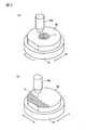
[圖4]揭示雷射光束照射工程的立體圖。[Figure 4] A three-dimensional view of the laser beam irradiation project.
[圖5]揭示晶圓剝離工程的立體圖。[Fig. 5] A perspective view showing the wafer peeling process.
以下,針對本發明實施形態的雷射加工裝置,及GaN晶圓的產生方法的實施形態,參照圖面詳細進行說明。Hereinafter, the laser processing apparatus according to the embodiment of the present invention and the embodiment of the GaN wafer production method will be described in detail with reference to the drawings.
圖1所示之雷射加工裝置2係具備基台4、保持被加工物的保持手段6、移動保持手段6的移動手段8、雷射光束照射手段10、攝像手段12、顯示手段14、剝離手段16、及未圖示的控制手段。The
保持手段6係包含可於X方向中自由移動地搭載於基台4之矩形狀的X方向可動板20、可於Y方向中自由移動地搭載於X方向可動板20之矩形狀的Y方向可動板22、及可自由旋轉地搭載於Y方向可動板22的上面之圓筒形狀的吸盤台24。再者,X方向是圖1中以箭頭X所示的方向,Y方向是以箭頭Y所示的方向,且正交於X方向的方向。X方向、Y方向所規定的平面係實施上的水平面。The holding means 6 includes a rectangular X-direction
移動手段8係包含X方向移動手段26、Y方向移動手段28、及旋轉手段(未圖示)。X方向移動手段26係具有於基台4上延伸於X方向的滾珠螺桿30,與連結於滾珠螺桿30之一方端部的馬達32。滾珠螺桿30的螺帽部(未圖示)被固定於X方向可動板20的下面。然後,X方向移動手段26係藉由滾珠螺桿30將馬達32的旋轉運動轉換成直線運動而傳達至X方向可動板20,沿著基台4上的導引軌道4a,使X方向可動板20於X方向中進退。Y方向移動手段28係具有於X方向可動板20上延伸於Y方向的滾珠螺桿34,與連結於滾珠螺桿34之一方端部的馬達36。滾珠螺桿34的螺帽部(未圖示)被固定於Y方向可動板22的下面。然後,Y方向移動手段28係藉由滾珠螺桿34將馬達36的旋轉運動轉換成直線運動而傳達至Y方向可動板22,沿著X方向可動板20上的導引軌道20a,使Y方向可動板22於Y方向中進退。旋轉手段係具有內藏於吸盤台24的馬達(未圖示),使吸盤台24對於Y方向可動板22旋轉。The moving means 8 includes an X-direction moving means 26, a Y-direction moving means 28, and a rotating means (not shown). The X-direction moving means 26 includes a
雷射光束照射手段10係藉由從基台4的上面向上方延伸的支持構件38支持,配置於實質水平地延伸的殼體39內,包含配設於殼體39之前端下面的聚光器10a。The laser beam irradiation means 10 is supported by a
攝像手段12係與聚光器10a在X方向隔開間隔而配設於殼體39的前端下面。攝像手段12係包含藉由可視光線進行攝像之一般的攝像元件(CCD)、對被加工物照射紅外線的紅外線照射手段、捕捉藉由紅外線照射手段所照射之紅外線的光學系、對應該光學系所捕捉的紅外線而輸出電性訊號的攝像元件(紅外線CCD)(任一皆未圖示)。顯示藉由攝像手段12所攝像之畫像的顯示手段14,係被搭載於殼體39前端上面。The imaging means 12 is spaced apart from the
剝離手段16係包含從基台4上的導引軌道4a的結束端部向上方延伸的框體42,與從可於Z方向中自由移動地連結於框體42的基端向X方向延伸的機械臂44。於框體42,內藏有使機械臂44進退於Z方向的Z方向移動手段(未圖示)。於機械臂44的前端,附設有馬達46,於馬達的下面,能以延伸於Z方向的軸線為中心自由旋轉地連結有圓盤狀的吸附片48。吸附片48係於下面(吸附面)形成複數吸附孔,藉由未圖示的流通路徑而連接於未圖示的吸引手段。又,於吸附片48,內藏有對於下面賦予超音波振動的超音波振動賦予手段(未圖示)。The peeling means 16 includes a
雷射加工裝置2係具備由電腦所成的控制手段(未圖示),藉由遵從控制程式而進行運算處裡的中央運算處理裝置(CPU)、儲存控制程式等的唯讀記憶體(ROM)、暫時記憶運算結果等的隨機存取記憶體(RAM)等所構成。該控制手段係電性連接於該雷射加工裝置的移動手段8、雷射光束照射手段10、攝像手段12、顯示手段14、及剝離手段16等,控制該等的作動。The
針對本發明實施形態的雷射光束照射手段10,使用圖2詳細說明。The laser beam irradiation means 10 according to the embodiment of the present invention will be described in detail with reference to FIG. 2.
該雷射光束照射手段10係由對被加工物照射雷射光束LB的聚光器10a、對雷射光束LB進行振盪的雷射振盪器10b、將從雷射振盪器10b振盪的雷射光束LB導引至聚光器10a的反射板10c所構成。雷射振盪器10b係具備以成為種源光(Seed light)的低輸出對高頻的脈衝雷射LB1進行振盪的種源機101、以所定重複頻率疏化該種源機101所振盪之高頻的脈衝雷射LB1,作為1突波脈衝BP而產生複數個高頻脈衝(在本實施形態中為3脈衝,以下,稱為「次脈衝」)之作為疏化部的聲光調變器(Acousto-Optic Modulator:以下,稱為「AOM」)102、吸收藉由AOM102的繞射光柵作用而被疏化之脈衝雷射的阻尼器103、放大透射AOM102,藉由由複數個次脈衝所成之突波脈衝BP所構成的脈衝雷射LB2的放大器104。The laser beam irradiation means 10 is composed of a
AOM102係例如具備由亞碲酸鹽系玻璃所成的聲光媒體,於該聲光媒體接著有未圖示的壓電元件。該聲光媒體係藉由壓電元件傳達超音波振動時,產生光彈性效應所致之繞射光柵的作用者,連接有用以對於AOM102的壓電元件,產生任意超音波振動的AOM控制手段105。然後,藉由控制AOM控制手段105,可將透射AOM102而構成突波脈衝BP之次脈衝的脈衝數,形成為任意數。該等種源機101、AOM控制手段105、放大器104係藉由雷射加工裝置2所具備之未圖示的控制手段適當控制。The AOM102 system includes, for example, an acousto-optic medium made of tellurite-based glass, and a piezoelectric element (not shown) is attached to the acousto-optic medium. The acousto-optic medium is a diffractive grating that produces a photoelastic effect when ultrasonic vibration is transmitted through piezoelectric elements, and it is connected to an AOM control means that can generate arbitrary ultrasonic vibrations for AOM102
於本實施形態之雷射加工裝置2中,從GaN晶棒產生GaN的晶圓時,雷射光束照射手段10係照射放大由複數個次脈衝所成之突波脈衝BP所構成的脈衝雷射LB2而產生的雷射光束LB。對於為了利用將該雷射光束LB的聚光點在GaN晶棒內部中定位於預定剝離的所定高度位置,並照射至成為界面的整面,有效率地獲得GaN晶圓來說,適切決定構成1個突波脈衝BP之次脈衝的脈衝數為佳。以下,針對決定構成1個突波脈衝BP之次脈衝的脈衝數的方法進行說明。In the
本實施形態的雷射加工裝置2係如圖3(a)所示,為了從被加工物即GaN晶棒60產生具有150μm之厚度的GaN晶圓,將雷射光束的聚光點定位照射於從GaN晶棒的表面離開150μm的位置。因此,為了決定構成1突波脈衝BP之適切的次脈衝的脈衝數,試驗性地於相同的位置實施雷射加工,形成1條雷射加工痕P。The
於圖3(b),揭示從上方觀看試驗性地進行雷射加工的GaN晶棒60的俯視圖之一部分放大圖。於以藉由該雷射加工所形成之雷射加工痕P為中心的水平方向,形成GaN晶棒被分離成Ga與N的破壞層B。揭示將從上段構成1個突波脈衝之次脈衝數設為2脈衝而形成突波脈衝之狀況,同樣地將次脈衝數設為3脈衝之狀況,將次脈衝設為7脈衝之狀況。由圖中可知,在次脈衝為2脈衝時,於以加工痕P為中心的水平方向,延伸有約230μm的破壞層B。同樣地,次脈衝為3脈衝時是680μm,次脈衝為7脈衝時是50μm,可確認分別有破壞層B延伸之狀況。於圖3(c)揭示在將次脈衝的個數設為2~10脈衝之間實施此種試驗性的雷射加工,測定破壞層B延伸於水平方向的平均長度的結果。In FIG. 3(b), a partially enlarged view of a top view of a
根據該等結果,可理解構成1突波脈衝的次脈衝之脈衝數的最佳值為3個。亦即,從GaN晶棒產生GaN晶圓時,將次脈衝設定為3個來構成1個突波脈衝而照射雷射光束的話,於GaN晶棒內部的界面中形成剝離面時,可將雷射光束的間隔擴張成最大,可利用更少的雷射加工量,有效率地產生剝離GaN晶圓的剝離面。再者,根據進行雷射加工時的加工條件、欲產生之GaN晶圓的厚度、加工之GaN晶圓的品質等,也想定該最佳次脈衝不是3個之狀況。此時,如上所述,試驗性進行雷射加工,求出於聚光點被定位的界面位置中破壞層延伸最長之次脈衝的脈衝數,適用於實際的雷射加工即可。From these results, it can be understood that the optimal number of pulses constituting one burst pulse is three. That is, when a GaN wafer is produced from a GaN ingot, if the sub-pulse is set to three to form a burst pulse and the laser beam is irradiated, when a peeling surface is formed in the interface inside the GaN ingot, the The interval between the beams is expanded to the maximum, and a smaller amount of laser processing can be used to efficiently produce a peeling surface for peeling the GaN wafer. Furthermore, depending on the processing conditions during laser processing, the thickness of the GaN wafer to be produced, the quality of the processed GaN wafer, etc., it is also assumed that the optimal number of sub-pulses is not three. At this time, as described above, laser processing is carried out experimentally, and the number of pulses of the second pulse with the longest extension of the damaged layer in the interface position where the condensing point is located can be calculated and applied to actual laser processing.
依據本發明所構成的雷射加工裝置2,係大概如上所述般構成者,針對使用本實施形態的雷射加工裝置2所實施之GaN晶圓的產生方法,以下詳細進行說明。The
首先,如圖1所示,將GaN晶棒60的背面固定於作為保持手段之吸盤台24的上面。該固定可使用例如環氧樹脂系接著劑等來固定(保持工程)。將GaN晶棒固定於吸盤台24之後,實施校準工程。在校準工程中,首先,藉由移動手段8使吸盤台24移動至攝像手段12的下方,藉由攝像手段12對GaN晶棒60進行攝像。接下來,依據藉由攝像手段12所攝像之GaN晶棒60的畫像,檢測出GaN晶棒60的外周,及形成於外周的缺口(定向平面),並且使吸盤台24移動、旋轉,進行GaN晶棒60與聚光器10a的對位,以加工開始時從聚光器10a照射的雷射光束LB,成為GaN晶棒60的中心位置之方式設定。接下來,藉由聚光點位置調整手段使聚光器10a往Z軸方向移動,將脈衝雷射的聚光點位置從GaN晶棒的表面調整至所定深度(150μm)的位置。First, as shown in FIG. 1, the back surface of the
將該聚光點位置定位於GaN晶棒的中心位置的話,如圖4(a)所示,朝GaN晶棒的中心,從聚光器10a照射藉由突波脈衝BP所構成之該雷射光束LB,並且藉由內藏於吸盤台24之馬達(未圖示)的作用來使吸盤台24旋轉,使Y方向移動手段28動作而讓吸盤台24往Y方向以所定速度移動。藉此,藉由雷射光束LB的照射所形成之雷射加工痕P,以從GaN晶棒的中心開始成為漩渦狀之方式形成(雷射光束照射工程)。If the condensing point is positioned at the center of the GaN ingot, as shown in FIG. 4(a), the laser formed by the burst pulse BP is irradiated toward the center of the GaN ingot from the
再者,本實施形態之雷射光束照射工程,係可在例如以下的加工條件下實施。In addition, the laser beam irradiation process of this embodiment can be implemented under the following processing conditions, for example.
雷射光束LB的波長:1064nmThe wavelength of the laser beam LB: 1064nm
高頻脈衝LB1的頻率:64MHzFrequency of high frequency pulse LB1: 64MHz
高頻脈衝LB1的脈衝時間寬度:315fsPulse time width of high frequency pulse LB1: 315fs
高頻脈衝LB1的脈衝時間間隔:15.6nsPulse time interval of high frequency pulse LB1: 15.6ns
雷射光束LB的重複頻率:100kHzRepetition frequency of laser beam LB: 100kHz
構成突波脈衝BP的次脈衝數:3個(可從2~10個中選擇)The number of sub-pulses constituting the burst pulse BP: 3 (can be selected from 2 to 10)
突波脈衝BP的時間寬度:31.2nsTime width of burst pulse BP: 31.2ns
放大後的雷射光束LB的平均輸出:1WAverage output of the amplified laser beam LB: 1W
每1突波脈衝的能量:1/100,000(J)Energy per burst pulse: 1/100,000(J)
數值孔徑(NA):0.8Numerical aperture (NA): 0.8
加工進給速度:100mm/sProcessing feed speed: 100mm/s
界面的位置:150μm(自晶棒表面起)The position of the interface: 150μm (from the surface of the ingot)
指數(index):600μmIndex: 600μm
再者,依據前述加工條件來照射雷射光束LB時的加工進給速度,係為了均勻形成剝離面的品質而維持為一定為佳。因此,從GaN晶棒的中心開始脈衝雷射的照射時,以使吸盤台旋轉的旋轉速度逐漸變慢之方式設定。又,在圖4(a)所示實施形態中,從GaN晶棒的中心開始雷射光束LB的照射,使吸盤台24的旋轉手段與Y方向移動手段28動作,將雷射加工痕P朝外方逐漸形成為漩渦狀,但是,對界面整體照射雷射光束LB的方法並不限定於此,例如,也可從GaN晶棒的最外周側開始雷射光束LB的照射,並將晶棒的中心設為終點。進而,如圖4(b)所示,在照射雷射光束LB,將雷射加工痕P形成於界面整體時,一邊使吸盤台24於X方向中直線地往返移動,一邊逐漸往Y方向移動,藉此對界面整體照射雷射光束LB亦可。In addition, the processing feed speed when irradiating the laser beam LB according to the aforementioned processing conditions is preferably maintained to be constant in order to uniformly form the quality of the peeling surface. Therefore, when starting the pulse laser irradiation from the center of the GaN crystal rod, it is set so that the rotation speed of the chuck table is gradually slowed down. Furthermore, in the embodiment shown in FIG. 4(a), the laser beam LB is irradiated from the center of the GaN ingot, and the rotating means of the chuck table 24 and the Y-direction moving means 28 are operated to turn the laser processing mark P toward The outer side is gradually formed into a vortex, but the method of irradiating the entire interface with the laser beam LB is not limited to this. For example, the laser beam LB may be irradiated from the outermost side of the GaN ingot, and the ingot The center of is set as the end point. Furthermore, as shown in FIG. 4(b), when the laser beam LB is irradiated to form the laser processing mark P on the entire interface, the chuck table 24 is moved linearly back and forth in the X direction while gradually moving in the Y direction Therefore, the entire interface may be irradiated with the laser beam LB.
如上所述,在本實施形態中,由複數個該高頻脈衝(次脈衝)構成1突波脈衝,放大其並照射雷射光束,據此,1脈衝(=1突波脈衝)的能量在1脈衝的時間寬度中分散而照射至界面位置,於GaN晶棒60的內部中階段性地GaN分離成Ga與N,可有效率地形成剝離面。尤其,在本實施形態中,作為次脈衝的脈衝數,選擇雷射光束LB的聚光點被定位的該界面位置中破壞層延伸最長的個數(3個),來形成突波脈衝,故對界面照射雷射光束LB時,可將鄰接之雷射光束照射位置的間隔隔開至最大。所以,可短時間結束雷射加工,更提升生產效率。As described above, in this embodiment, a plurality of these high-frequency pulses (subpulses) constitute one burst pulse, which is amplified and irradiated with a laser beam. According to this, the energy of one pulse (=1 burst pulse) is The pulse is dispersed in the time width of one pulse and irradiated to the interface position. In the inside of the
該雷射光束照射工程已結束的話,則實施晶圓剝離工程。在晶圓剝離工程中,首先,藉由移動手段8使吸盤台24移動至剝離手段16的吸附片48的下方。接下來,藉由未圖示的Z方向移動手段,讓機械臂44加工,如圖5所示般,使吸附片48的下面密接於GaN晶棒60的上面。接下來,使吸引手段動作,將吸附片48的下面吸附於GaN晶棒60的上面。接著,使超音波振動賦予手段動作,對於吸附片48的下面賦予超音波振動,並且使馬達46動作而使吸附片48旋轉。藉此,可將藉由上述雷射光束照射工程被照射雷射光束的界面設為剝離面,分離GaN晶棒60的一部分,可有效率地產生所希望之厚度(150μm)的晶圓62。產生GaN晶圓62之後,利用搬送至設置於基台4上之未圖示的研磨手段,研磨GaN晶棒60的上面,依序重複實施上述之雷射光束照射工程、晶圓剝離工程,可減少被廢棄之素材(GaN)的總量,從所定GaN晶棒,更有效率地產生大量的GaN晶圓。再者,在本實施形態中,藉由雷射加工裝置2所具備之剝離手段16,自動地實施晶圓的剝離工程,但是,用以剝離GaN晶圓的手段並不限定於此,例如,也可使用具備吸附面的器具,與具備把持該器具之把持部的治具,藉由作業者的手作業,來實施剝離工程。If the laser beam irradiation process is completed, the wafer stripping process will be implemented. In the wafer peeling process, first, the chuck table 24 is moved below the
10:雷射光束照射手段10: Laser beam irradiation method
10a:聚光器10a: Concentrator
10b:雷射振盪器10b: Laser oscillator
10c:反射板10c: reflector
24:吸盤台24: Suction table
60:GaN晶棒60: GaN ingot
101:種源機101: Seed Source Machine
102:聲光調變器(AOM)102: Acousto-optic modulator (AOM)
103:阻尼器103: Damper
104:放大器104: Amplifier
105:AOM控制手段105: AOM control means
BP:突波脈衝BP: burst pulse
LB:雷射光束LB: Laser beam
LB1、LB2:脈衝雷射LB1, LB2: Pulse laser
Claims (1)
Translated fromChineseApplications Claiming Priority (2)
| Application Number | Priority Date | Filing Date | Title |
|---|---|---|---|
| JP2016-107038 | 2016-05-30 | ||
| JP2016107038AJP6770340B2 (en) | 2016-05-30 | 2016-05-30 | How to generate a wafer |
Publications (2)
| Publication Number | Publication Date |
|---|---|
| TW201805099A TW201805099A (en) | 2018-02-16 |
| TWI705868Btrue TWI705868B (en) | 2020-10-01 |
Family
ID=60269171
Family Applications (1)
| Application Number | Title | Priority Date | Filing Date |
|---|---|---|---|
| TW106112631ATWI705868B (en) | 2016-05-30 | 2017-04-14 | Wafer production method |
Country Status (6)
| Country | Link |
|---|---|
| US (1) | US10870169B2 (en) |
| JP (1) | JP6770340B2 (en) |
| KR (1) | KR102238569B1 (en) |
| CN (1) | CN107442952B (en) |
| DE (1) | DE102017208953A1 (en) |
| TW (1) | TWI705868B (en) |
Families Citing this family (5)
| Publication number | Priority date | Publication date | Assignee | Title |
|---|---|---|---|---|
| DE102018133083A1 (en) | 2018-12-20 | 2020-06-25 | Carl Zeiss Jena Gmbh | Device and method for the controlled machining of a workpiece with machining radiation |
| JP7339031B2 (en) | 2019-06-28 | 2023-09-05 | 株式会社ディスコ | Laser processing equipment |
| JP7523932B2 (en)* | 2020-03-30 | 2024-07-29 | 株式会社ディスコ | Laser processing equipment |
| JP7500261B2 (en)* | 2020-04-10 | 2024-06-17 | 株式会社ディスコ | Wafer Production Method |
| JP7429080B1 (en) | 2023-11-28 | 2024-02-07 | 有限会社ドライケミカルズ | Semiconductor crystal wafer manufacturing equipment and manufacturing method |
Citations (3)
| Publication number | Priority date | Publication date | Assignee | Title |
|---|---|---|---|---|
| WO2012108054A1 (en)* | 2011-02-10 | 2012-08-16 | 信越ポリマー株式会社 | Production method for monocrystalline substrate and production method for monocrystalline member with modified layer formed therein |
| JP2012522374A (en)* | 2009-03-27 | 2012-09-20 | エレクトロ サイエンティフィック インダストリーズ インコーポレーテッド | Laser micromachining with tailored bursts of short laser pulses |
| JP2015110248A (en)* | 2013-12-03 | 2015-06-18 | ロフィン−ジナール テクノロジーズ インコーポレイテッド | Method and apparatus for laser-machining silicon by filamentation of burst ultrafast laser pulse |
Family Cites Families (11)
| Publication number | Priority date | Publication date | Assignee | Title |
|---|---|---|---|---|
| DE69842052D1 (en) | 1997-10-30 | 2011-01-27 | Sumitomo Electric Industries | GAN CRYSTAL SUBSTRATE AND MANUFACTURING METHOD |
| TW417315B (en)* | 1998-06-18 | 2001-01-01 | Sumitomo Electric Industries | GaN single crystal substrate and its manufacture method of the same |
| US7723642B2 (en)* | 1999-12-28 | 2010-05-25 | Gsi Group Corporation | Laser-based system for memory link processing with picosecond lasers |
| US20040134894A1 (en)* | 1999-12-28 | 2004-07-15 | Bo Gu | Laser-based system for memory link processing with picosecond lasers |
| AU2001227764A1 (en)* | 2000-01-10 | 2001-07-24 | Electro Scientific Industries, Inc. | Laser system and method for processing a memory link with a burst of laser pulses having ultrashort pulsewidths |
| FR2961948B1 (en)* | 2010-06-23 | 2012-08-03 | Soitec Silicon On Insulator | PROCESS FOR TREATING A COMPOUND MATERIAL PART |
| CN103236641A (en)* | 2012-11-08 | 2013-08-07 | 国神光电科技(上海)有限公司 | Device and method for generating envelop-adjustable ultrashort pulse sequences |
| JP2014104484A (en)* | 2012-11-27 | 2014-06-09 | Disco Abrasive Syst Ltd | Laser processing apparatus |
| US20150034613A1 (en)* | 2013-08-02 | 2015-02-05 | Rofin-Sinar Technologies Inc. | System for performing laser filamentation within transparent materials |
| JP6390898B2 (en)* | 2014-08-22 | 2018-09-19 | アイシン精機株式会社 | Substrate manufacturing method, workpiece cutting method, and laser processing apparatus |
| CN104625433A (en)* | 2014-12-31 | 2015-05-20 | 武汉华工激光工程有限责任公司 | Method for cutting LED lamp filament transparent material support |
- 2016
- 2016-05-30JPJP2016107038Apatent/JP6770340B2/enactiveActive
- 2017
- 2017-04-14TWTW106112631Apatent/TWI705868B/enactive
- 2017-05-16CNCN201710341747.7Apatent/CN107442952B/enactiveActive
- 2017-05-17KRKR1020170060934Apatent/KR102238569B1/enactiveActive
- 2017-05-22USUS15/601,321patent/US10870169B2/enactiveActive
- 2017-05-29DEDE102017208953.9Apatent/DE102017208953A1/enactivePending
Patent Citations (3)
| Publication number | Priority date | Publication date | Assignee | Title |
|---|---|---|---|---|
| JP2012522374A (en)* | 2009-03-27 | 2012-09-20 | エレクトロ サイエンティフィック インダストリーズ インコーポレーテッド | Laser micromachining with tailored bursts of short laser pulses |
| WO2012108054A1 (en)* | 2011-02-10 | 2012-08-16 | 信越ポリマー株式会社 | Production method for monocrystalline substrate and production method for monocrystalline member with modified layer formed therein |
| JP2015110248A (en)* | 2013-12-03 | 2015-06-18 | ロフィン−ジナール テクノロジーズ インコーポレイテッド | Method and apparatus for laser-machining silicon by filamentation of burst ultrafast laser pulse |
Also Published As
| Publication number | Publication date |
|---|---|
| TW201805099A (en) | 2018-02-16 |
| KR20170135684A (en) | 2017-12-08 |
| CN107442952A (en) | 2017-12-08 |
| JP2017216266A (en) | 2017-12-07 |
| KR102238569B1 (en) | 2021-04-08 |
| DE102017208953A1 (en) | 2017-11-30 |
| US20170341179A1 (en) | 2017-11-30 |
| US10870169B2 (en) | 2020-12-22 |
| CN107442952B (en) | 2021-08-03 |
| JP6770340B2 (en) | 2020-10-14 |
Similar Documents
| Publication | Publication Date | Title |
|---|---|---|
| TWI705868B (en) | Wafer production method | |
| KR102346916B1 (en) | METHOD OF GENERATING POLYCRYSTALLINE SiC WAFER | |
| TWI683737B (en) | Wafer generation method | |
| TWI730141B (en) | SiC wafer generation method | |
| TW201639016A (en) | Wafer generation method | |
| JP4843212B2 (en) | Laser processing apparatus and laser processing method | |
| TW201639017A (en) | Wafer generation method | |
| TW201706066A (en) | Wafer producing method | |
| TW201639018A (en) | Wafer producing method | |
| TW201635363A (en) | Wafer producing method | |
| CN103223558B (en) | Laser processing device | |
| TW201631227A (en) | Wafer producing method | |
| TW201631228A (en) | Wafer producing method | |
| TW201735143A (en) | SiC wafer producing method | |
| TW201622935A (en) | Production method for wafer | |
| TW201635364A (en) | Wafer producing method | |
| TW201700249A (en) | Wafer producing method | |
| CN110277349A (en) | Wafer production method and wafer production device | |
| TWI743297B (en) | Laser processing device | |
| CN102785028A (en) | Laser processing method and laser processing apparatus | |
| TW201707822A (en) | Wafer generation method | |
| TW201625393A (en) | Wafer formation method | |
| TWI759533B (en) | Laser processing equipment | |
| JP2019098359A (en) | Laser processing method for wafer | |
| CN107363422B (en) | Laser processing device |