TWI705666B - Transmission device, receiving device, communication system - Google Patents
Transmission device, receiving device, communication systemDownload PDFInfo
- Publication number
- TWI705666B TWI705666BTW105113163ATW105113163ATWI705666BTW I705666 BTWI705666 BTW I705666BTW 105113163 ATW105113163 ATW 105113163ATW 105113163 ATW105113163 ATW 105113163ATW I705666 BTWI705666 BTW I705666B
- Authority
- TW
- Taiwan
- Prior art keywords
- signal
- clock signal
- differential
- blanking
- circuit
- Prior art date
Links
Images


Classifications
- H—ELECTRICITY
- H04—ELECTRIC COMMUNICATION TECHNIQUE
- H04L—TRANSMISSION OF DIGITAL INFORMATION, e.g. TELEGRAPHIC COMMUNICATION
- H04L7/00—Arrangements for synchronising receiver with transmitter
- H04L7/0016—Arrangements for synchronising receiver with transmitter correction of synchronization errors
- H04L7/002—Arrangements for synchronising receiver with transmitter correction of synchronization errors correction by interpolation
- H04L7/0025—Arrangements for synchronising receiver with transmitter correction of synchronization errors correction by interpolation interpolation of clock signal
- H—ELECTRICITY
- H04—ELECTRIC COMMUNICATION TECHNIQUE
- H04L—TRANSMISSION OF DIGITAL INFORMATION, e.g. TELEGRAPHIC COMMUNICATION
- H04L25/00—Baseband systems
- H04L25/38—Synchronous or start-stop systems, e.g. for Baudot code
- H04L25/40—Transmitting circuits; Receiving circuits
- H—ELECTRICITY
- H04—ELECTRIC COMMUNICATION TECHNIQUE
- H04L—TRANSMISSION OF DIGITAL INFORMATION, e.g. TELEGRAPHIC COMMUNICATION
- H04L25/00—Baseband systems
- H04L25/02—Details ; arrangements for supplying electrical power along data transmission lines
- H04L25/0264—Arrangements for coupling to transmission lines
- H04L25/0272—Arrangements for coupling to multiple lines, e.g. for differential transmission
- H—ELECTRICITY
- H04—ELECTRIC COMMUNICATION TECHNIQUE
- H04L—TRANSMISSION OF DIGITAL INFORMATION, e.g. TELEGRAPHIC COMMUNICATION
- H04L25/00—Baseband systems
- H04L25/38—Synchronous or start-stop systems, e.g. for Baudot code
- H—ELECTRICITY
- H04—ELECTRIC COMMUNICATION TECHNIQUE
- H04L—TRANSMISSION OF DIGITAL INFORMATION, e.g. TELEGRAPHIC COMMUNICATION
- H04L7/00—Arrangements for synchronising receiver with transmitter
- H—ELECTRICITY
- H04—ELECTRIC COMMUNICATION TECHNIQUE
- H04L—TRANSMISSION OF DIGITAL INFORMATION, e.g. TELEGRAPHIC COMMUNICATION
- H04L7/00—Arrangements for synchronising receiver with transmitter
- H04L7/0016—Arrangements for synchronising receiver with transmitter correction of synchronization errors
- H04L7/002—Arrangements for synchronising receiver with transmitter correction of synchronization errors correction by interpolation
- H04L7/0029—Arrangements for synchronising receiver with transmitter correction of synchronization errors correction by interpolation interpolation of received data signal
- H—ELECTRICITY
- H04—ELECTRIC COMMUNICATION TECHNIQUE
- H04L—TRANSMISSION OF DIGITAL INFORMATION, e.g. TELEGRAPHIC COMMUNICATION
- H04L7/00—Arrangements for synchronising receiver with transmitter
- H04L7/04—Speed or phase control by synchronisation signals
- H—ELECTRICITY
- H04—ELECTRIC COMMUNICATION TECHNIQUE
- H04L—TRANSMISSION OF DIGITAL INFORMATION, e.g. TELEGRAPHIC COMMUNICATION
- H04L7/00—Arrangements for synchronising receiver with transmitter
- H04L7/04—Speed or phase control by synchronisation signals
- H04L7/06—Speed or phase control by synchronisation signals the synchronisation signals differing from the information signals in amplitude, polarity or frequency or length
- H04L7/065—Speed or phase control by synchronisation signals the synchronisation signals differing from the information signals in amplitude, polarity or frequency or length and superimposed by modulation
- Y—GENERAL TAGGING OF NEW TECHNOLOGICAL DEVELOPMENTS; GENERAL TAGGING OF CROSS-SECTIONAL TECHNOLOGIES SPANNING OVER SEVERAL SECTIONS OF THE IPC; TECHNICAL SUBJECTS COVERED BY FORMER USPC CROSS-REFERENCE ART COLLECTIONS [XRACs] AND DIGESTS
- Y02—TECHNOLOGIES OR APPLICATIONS FOR MITIGATION OR ADAPTATION AGAINST CLIMATE CHANGE
- Y02D—CLIMATE CHANGE MITIGATION TECHNOLOGIES IN INFORMATION AND COMMUNICATION TECHNOLOGIES [ICT], I.E. INFORMATION AND COMMUNICATION TECHNOLOGIES AIMING AT THE REDUCTION OF THEIR OWN ENERGY USE
- Y02D30/00—Reducing energy consumption in communication networks
- Y02D30/70—Reducing energy consumption in communication networks in wireless communication networks
Landscapes
- Engineering & Computer Science (AREA)
- Computer Networks & Wireless Communication (AREA)
- Signal Processing (AREA)
- Power Engineering (AREA)
- Dc Digital Transmission (AREA)
Abstract
Translated fromChineseDescription
Translated fromChinese本揭示係關於應用於資料信號與時脈信號之傳輸之傳送裝置、接收裝置、及通信系統、以及信號傳送方法、信號接收方法、及通信方法。The present disclosure relates to a transmitting device, a receiving device, and a communication system, as well as a signal transmission method, a signal receiving method, and a communication method applied to the transmission of data signals and clock signals.
近年來,於智慧型手機等行動裝置或相機裝置等,處理之圖像資料朝大容量化進展,故謀求裝置內或不同裝置間的資料傳輸之高速化且低消耗電力化。為了對應此種要求,作為適於行動裝置或相機裝置之連接介面,MIPI(Mobile Industry Processor Interface:行動產業處理器介面)聯盟所訂定之C-PHY規格或D-PHY規格之類的高速介面規格之標準化持續發展。C-PHY規格或D-PHY規格為通信協定之實體層(physical layer:PHY)之介面規格。又,作為C-PHY規格或D-PHY規格之上階協定層,存在適於行動裝置之顯示器之DSI(Display Serial Interface:顯示器串列介面)、或適於相機裝置之CSI(Camera Serial Interface:相機串列介面)。專利文獻1中乃提出謀求D-PHY規格之信號傳送之穩定化之技術。In recent years, in mobile devices such as smartphones, camera devices, etc., the processing of image data has been increasing in volume. Therefore, data transmission within the device or between different devices is sought to increase speed and reduce power consumption. In order to meet this requirement, as a connection interface suitable for mobile devices or camera devices, the MIPI (Mobile Industry Processor Interface: Mobile Industry Processor Interface) alliance stipulates high-speed interface specifications such as C-PHY specifications or D-PHY specifications The standardization continues to develop. The C-PHY specification or the D-PHY specification is the interface specification of the physical layer (PHY) of the communication protocol. In addition, as the upper-level protocol layer of the C-PHY specification or D-PHY specification, there are DSI (Display Serial Interface) suitable for displays of mobile devices, or CSI (Camera Serial Interface: Camera serial interface).
[專利文獻1]日本專利特表2014-522204號公報[Patent Document 1] Japanese Patent Publication No. 2014-522204
於上述C-PYH規格或D-PHY規格中,對實質性資料信號之傳輸使用高度(High Speed:HS)差動信號。又,於時脈信號及資料信號之消隱期間使用低功率(Low Power:LP)信號。HS差動信號與LP信號以共通之傳輸路徑傳輸。例如於D-PHY規格中,存在傳輸時脈信號之1個傳輸路徑(時脈通道)、與傳輸資料信號之1個或複數個傳輸路徑(資料通道)。於時脈通道與資料通道各者之信號傳輸期間,存在以HS差動信號進行傳輸之期間與以LP信號進行傳輸之期間。於時脈通道與資料通道各者中,以共通之傳輸路徑傳輸HS差動信號與LP信號。然而,LP信號非差動信號而是單端信號,又,信號傳輸所需要之電壓值與HS差動信號不同。因此,用以傳輸接收HS差動信號與LP信號各者之電路需分開。In the above-mentioned C-PYH specification or D-PHY specification, high speed (HS) differential signals are used for the transmission of substantial data signals. In addition, a Low Power (LP) signal is used during the blanking period of the clock signal and the data signal. The HS differential signal and the LP signal are transmitted through a common transmission path. For example, in the D-PHY specification, there are one transmission path (clock channel) for transmitting clock signals, and one or more transmission paths (data channels) for transmitting data signals. During the signal transmission period of each of the clock channel and the data channel, there are a period of transmission by HS differential signal and a period of transmission by LP signal. In each of the clock channel and the data channel, the HS differential signal and the LP signal are transmitted through a common transmission path. However, the LP signal is not a differential signal but a single-ended signal, and the voltage value required for signal transmission is different from the HS differential signal. Therefore, the circuits used to transmit and receive the HS differential signal and the LP signal must be separated.
期望提供一種可謀求資料傳輸時之低消耗電力化之傳送裝置、接收裝置、及通信系統、以及信號傳送方法、信號接收方法、及通信方法。It is desirable to provide a transmission device, a receiving device, and a communication system, as well as a signal transmission method, a signal reception method, and a communication method that can achieve low power consumption during data transmission.
本揭示一實施形態之傳送裝置為具備以下者:時脈信號傳送電路,其將時脈信號輸出至時脈信號線;資料信號傳送電路,其將資料信號輸出至資料信號線;及消隱控制部,其控制時脈信號傳送電路,而與資料信號之消隱期間同步地自時脈信號傳送電路向時脈信號線取代時脈信號而輸出特定之消隱信號。The transmission device of an embodiment of the present disclosure is provided with the following: a clock signal transmission circuit, which outputs a clock signal to the clock signal line; a data signal transmission circuit, which outputs a data signal to the data signal line; and blanking control Part, which controls the clock signal transmission circuit and outputs a specific blanking signal from the clock signal transmission circuit to the clock signal line to replace the clock signal in synchronization with the blanking period of the data signal.
本揭示一實施形態之接收裝置為具備以下者:資料信號接收電路,其經由資料信號線接收資料信號;與時脈信號接收電路,其經由時脈信號線接收時脈信號、與與資料信號之消隱期間同步輸出之特定之消隱信號。The receiving device of an embodiment of the present disclosure is provided with the following: a data signal receiving circuit, which receives a data signal through a data signal line; and a clock signal receiving circuit, which receives a clock signal through a clock signal line, and a data signal The specific blanking signal output synchronously during blanking period.
本揭示一實施形態之通信系統為具備以下者:傳送裝置,其將時脈信號輸出至時脈信號線,將資料信號輸出至資料信號線,且與資料信號之消隱期間同步地取代時脈信號而輸出特定之消隱信號;及接收裝置,其經由資料信號線接收資料信號,經由時脈信號線接收時脈信號與特定之消隱信號。The communication system of one embodiment of the present disclosure is provided with the following: a transmission device that outputs a clock signal to the clock signal line, outputs a data signal to the data signal line, and replaces the clock synchronously with the blanking period of the data signal Signal and output a specific blanking signal; andThe receiving device receives the data signal via the data signal line, and receives the clock signal and the specific blanking signal via the clock signal line.
本揭示一實施形態之信號傳送方法為包含以下者:將時脈信號輸出至時脈信號線;將資料信號輸出至資料信號線;及與資料信號之消隱期間同步地向時脈信號線取代時脈信號而輸出特定之消隱信號。The signal transmission method of an embodiment of the present disclosure includes the following: outputting the clock signal to the clock signal line; outputting the data signal to the data signal line; and replacing the clock signal line in synchronization with the blanking period of the data signal Clock signal and output a specific blanking signal.
本揭示一實施形態之信號接收方法為包含以下者:經由資料信號線接收資料信號;及經由時脈信號線接收時脈信號、及與資料信號之消隱期間同步輸出之特定之消隱信號。The signal receiving method of an embodiment of the present disclosure includes the following: receiving a data signal via a data signal line; and receiving a clock signal via a clock signal line, and a specific blanking signal output in synchronization with the blanking period of the data signal.
本揭示一實施形態之通信方法為包含以下者:將時脈信號輸出至時脈信號線;將資料信號輸出至資料信號線;與資料信號之消隱期間同步地向時脈信號線取代時脈信號而輸出特定之消隱信號;經由上述資料信號線接收上述資料信號;及經由時脈信號線接收時脈信號與特定之消隱信號。The communication method of an embodiment of the present disclosure includes the following: outputting a clock signal to a clock signal line; outputting a data signal to a data signal line; replacing the clock with the clock signal line in synchronization with the blanking period of the data signal Signal and output a specific blanking signal; receive the data signal via the data signal line; and receive a clock signal and a specific blanking signal via a clock signal line.
於本揭示一實施形態之傳送裝置或通信系統、或信號傳送方法或通信方法中,於資料信號之消隱期間同步地向時脈信號線取代時脈信號而輸出特定之消隱信號。In the transmission device or communication system, or signal transmission method or communication method of an embodiment of the present disclosure, a specific blanking signal is output to the clock signal line instead of the clock signal in synchronization during the blanking period of the data signal.
於本揭示一實施形態之接收裝置或通信系統、或信號接收方法或通信方法中,經由時脈信號線而接收時脈信號、及與資料信號之消隱期間同步輸出之特定之消隱信號。In the receiving device or communication system, or signal receiving method or communication method of an embodiment of the present disclosure, a clock signal is received via a clock signal line, and a specific blanking signal is output synchronously with the blanking period of the data signal.
根據本揭示一實施形態之傳送裝置或通信系統、或信號傳送方法或通信方法,由於與資料信號之消隱期間同步地向時脈信號線取代時脈信號而輸出特定之消隱信號,故可謀求資料傳輸時之低消耗電力化。According to the transmission device or communication system, or signal transmission method or communication method of an embodiment of the present disclosure, since a specific blanking signal is output to the clock signal line instead of the clock signal in synchronization with the blanking period of the data signal, it is possible to Seek low power consumption during data transmission.
根據本揭示一實施形態之接收裝置或通信系統、或信號接收方法或通信方法,由於經由時脈信號線而接收時脈信號、及與資料信號之消隱期間同步輸出之特定之消隱信號,故可謀求資料傳輸時之低消耗電力化。According to the receiving device or communication system, or signal receiving method or communication method according to an embodiment of the present disclosure, since the clock signal is received via the clock signal line, and the specific blanking signal is output synchronously with the blanking period of the data signal, Therefore, low consumption can be sought in data transmissionPower consumption.
另,此處記載之效果並非限定者,可為本揭示中所記載之任意效果。In addition, the effect described here is not limited, and may be any effect described in this disclosure.
1:傳送部1: Transmission Department
1B:傳送部1B: Transmission Department
2:接收部2: receiving part
2A:接收部2A: Receiving Department
2B:接收部2B: Receiving Department
11:CL-HS電路11: CL-HS circuit
12:CL-LP電路12: CL-LP circuit
13:DL-HS電路13: DL-HS circuit
15:切換開關15: Toggle switch
16:切換開關16: toggle switch
17:選擇器17: selector
18:選擇器18: selector
20:消隱控制部20: Blanking control section
21:CL-HS電路21: CL-HS circuit
22:CL-LP電路22: CL-LP circuit
23:DL-HS電路23: DL-HS circuit
24:CL-LP電路24: CL-LP circuit
25~28:選擇器25~28: selector
30:時脈信號線30: Clock signal line
31~34:資料信號線31~34: Data signal line
41:LP狀態機(LP FSM)41: LP State Machine (LP FSM)
42:LP編碼器(LP ENC)42: LP encoder (LP ENC)
43:LP驅動器(LP DRV)43: LP drive (LP DRV)
44:LP接收器(LP RCV)44: LP receiver (LP RCV)
45:LP解碼器(LP DEC)45: LP decoder (LP DEC)
46:LP狀態機(LP FSM)46: LP State Machine (LP FSM)
51:HS狀態機(HS FSM)51: HS State Machine (HS FSM)
52:選擇器52: selector
53:並列/串列(PS)轉換電路53: Parallel/serial (PS) conversion circuit
54:時脈分頻器(DIV)54: Clock divider (DIV)
55:HS驅動器(HS DRV)55: HS drive (HS DRV)
56:終端電路(TERM)56: terminal circuit (TERM)
57:HS接收器(HS RCV)57: HS receiver (HS RCV)
58:時脈分頻器(DIV)58: Clock divider (DIV)
59:時脈狀態判別電路59: Clock state discrimination circuit
61:LP狀態機(LP FSM)61: LP State Machine (LP FSM)
62:LP編碼器(LP ENC)62: LP encoder (LP ENC)
63:LP驅動器(LP DRV)63: LP drive (LP DRV)
64:LP接收器(LP RCV)64: LP receiver (LP RCV)
65:LP解碼器(LP DEC)65: LP decoder (LP DEC)
66:LP狀態機(LP FSM)66: LP State Machine (LP FSM)
71:HS狀態機(HS FSM)71: HS State Machine (HS FSM)
72:選擇器72: selector
73:並列/串列(PS)轉換電路73: Parallel/serial (PS) conversion circuit
74:HS驅動器(HS DRV)74: HS drive (HS DRV)
75:終端電路(TERM)75: terminal circuit (TERM)
76:HS接收器(HS RCV)76: HS receiver (HS RCV)
77:時脈分頻器(DIV)77: Clock divider (DIV)
78:字元對齊修正電路(ALN)78: Character alignment correction circuit (ALN)
81:PLL電路81: PLL circuit
82:水晶振盪器(XTAL)82: Crystal oscillator (XTAL)
83:水晶振盪器(XTAL)83: Crystal oscillator (XTAL)
84:PLL電路84: PLL circuit
101:傳送部101: Transmission Department
102:接收部102: receiving department
111:CL-HS電路111: CL-HS circuit
112:CL-LP電路112: CL-LP circuit
113:DL-HS電路113: DL-HS circuit
114:DL-LP電路114: DL-LP circuit
121:CL-HS電路121: CL-HS circuit
122:CL-LP電路122: CL-LP circuit
123:DL-HS電路123: DL-HS circuit
124:DL-LP電路124: DL-LP circuit
300:智慧型手機300: smart phone
301:車輛301: Vehicle
302:ECU302: ECU
310:應用處理器310: Application processor
311:CPU311: CPU
312:記憶體控制部312: Memory Control Unit
313:電源控制部313: Power Control Department
314:外部介面部314: external face
315:GPU315: GPU
316:媒體處理部316: Media Processing Department
317:顯示器控制部317: Display Control Department
318:MIPI介面部318: MIPI face
319:系統匯流排319: system bus
401~404:車載用相機401~404: Car cameras
410:影像感測器410: Image Sensor
411:感測器部411: Sensor Department
412:ISP412: ISP
413:JPEG編碼部413: JPEG encoding department
414:CPU414: CPU
415:RAM415: RAM
416:ROM416: ROM
417:電源控制部417: Power Control Department
418:I2C介面418: I2 C interface
419:MIPI介面419: MIPI interface
420:系統匯流排420: system bus
431:影像感測器431: Image Sensor
432:DSP電路432: DSP circuit
433:選擇器433: selector
434:SerDes電路434: SerDes circuit
441:連接介面441: connection interface
442:連接介面442: connection interface
501:記憶體501: memory
502:無線通信部502: Wireless Communications Department
504:顯示器504: Display
a:範圍a: range
ALL0:信號ALL0: signal
ALL1:信號ALL1: signal
b:範圍b: range
c:範圍c: range
CL:時脈通道CL: clock channel
d:範圍d: range
DL:資料通道DL: Data channel
DL1~DL4:資料通道DL1~DL4: Data channel
Dn:負信號線Dn: negative signal line
Dp:正信號線Dp: positive signal line
LPS:低功率狀態LPS: Low power state
HPS:高速狀態HPS: High-speed state
HS-0:差動信號HS-0: Differential signal
HS-1:差動信號HS-1: Differential signal
HST:實質性資料信號HST: Substantial Data Signal
RX:接收部RX: receiving part
RxActiveHS:接收主動信號RxActiveHS: receive active signal
RX-ANALOG:接收類比電路RX-ANALOG: Receive analog circuit
RX-DIGITAL:接收數位電路RX-DIGITAL: Receive digital circuit
RxDataHS:接收資料RxDataHS: Receive data
RxSyncHS:接收同步信號RxSyncHS: receive synchronization signal
RxValidHS:接收有效信號RxValidHS: receive valid signal
S101~S106:步驟S101~S106: steps
SYNC:同步編碼信號SYNC: Synchronous coding signal
THS-SYNC:SYNC(同步)期間THS-SYNC : During SYNC (synchronization)
THS-TRAIL:TRAIL期間THS-TRAIL : During TRAIL
Toggle:信號Toggle: Signal
TX:傳送部TX: Transmission Department
TX-ANALOG:傳送類別電路TX-ANALOG: Transmission category circuit
TxDataHS:傳送資料TxDataHS: Send data
TX-DIGITAL:傳送數位電路TX-DIGITAL: Transmission digital circuit
TxReadyHS:準備完成信號TxReadyHS: ready to complete signal
TxRequestHS:請求信號TxRequestHS: request signal
圖1係顯示傳輸資料信號與時脈信號之通信系統之概要之方塊圖。Figure 1 is a block diagram showing the outline of a communication system that transmits data signals and clock signals.
圖2係顯示實現圖1所示之通信系統之比較例之通信系統之一構成例之方塊圖。Fig. 2 is a block diagram showing a configuration example of a communication system that realizes the comparative example of the communication system shown in Fig. 1.
圖3係顯示圖2所示之通信系統之具體電路構成例之電路圖。FIG. 3 is a circuit diagram showing a specific circuit configuration example of the communication system shown in FIG. 2.
圖4係顯示於圖2所示之通信系統中傳輸至時脈通道與資料通道之各個信號波形之一例之說明圖。4 is an explanatory diagram showing an example of each signal waveform transmitted to the clock channel and the data channel in the communication system shown in FIG. 2.
圖5係顯示本揭示第1實施形態之通信系統之概要之方塊圖。Fig. 5 is a block diagram showing the outline of the communication system of the first embodiment of the present disclosure.
圖6係顯示圖5所示之通信系統之具體電路構成例之電路圖。FIG. 6 is a circuit diagram showing a specific circuit configuration example of the communication system shown in FIG. 5.
圖7係顯示於圖5所示之通信系統中傳輸至時脈通道與資料通道之各個信號波形之一例之說明圖。FIG. 7 is an explanatory diagram showing an example of each signal waveform transmitted to the clock channel and the data channel in the communication system shown in FIG. 5.
圖8係關於差動信號之說明圖。Fig. 8 is an explanatory diagram of the differential signal.
圖9係顯示第2實施形態之通信系統之具體電路構成例之電路圖。Fig. 9 is a circuit diagram showing a specific circuit configuration example of the communication system of the second embodiment.
圖10係顯示於圖9所示之通信系統中傳輸至時脈通道與資料通道之各個信號波形之一例之說明圖。FIG. 10 is an explanatory diagram showing an example of each signal waveform transmitted to the clock channel and the data channel in the communication system shown in FIG. 9.
圖11係顯示於第2實施形態之第1變化例之通信系統中傳輸至時脈通道與資料通道之各個信號波形之一例的說明圖。11 is an explanatory diagram showing an example of each signal waveform transmitted to the clock channel and the data channel in the communication system of the first modification of the second embodiment.
圖12係顯示於第2實施形態之第2變化例之通信系統中傳輸至時脈通道與資料通道之各個信號波形之一例的說明圖。12 is an explanatory diagram showing an example of each signal waveform transmitted to the clock channel and the data channel in the communication system of the second modification of the second embodiment.
圖13係顯示於第2實施形態之第3變化例之通信系統中傳輸至時脈通道與資料通道之各個信號波形之一例的說明圖。13 is an explanatory diagram showing an example of each signal waveform transmitted to the clock channel and the data channel in the communication system of the third modification of the second embodiment.
圖14係顯示於第2實施形態之第4變化例之通信系統中傳輸至時脈通道與資料通道之各個信號波形之一例的說明圖。14 is an explanatory diagram showing an example of each signal waveform transmitted to the clock channel and the data channel in the communication system of the fourth modification of the second embodiment.
圖15係顯示於第2實施形態之第5變化例之通信系統中傳輸至時脈通道與資料通道之各個信號波形之一例的說明圖。15 is an explanatory diagram showing an example of each signal waveform transmitted to the clock channel and the data channel in the communication system of the fifth modification of the second embodiment.
圖16係顯示第3實施形態之通信系統之概要之方塊圖。Fig. 16 is a block diagram showing the outline of the communication system of the third embodiment.
圖17係顯示圖16所示之通信系統之具體應用例之方塊圖。FIG. 17 is a block diagram showing a specific application example of the communication system shown in FIG. 16.
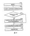
圖18係顯示圖17所示之應用例之資料傳送處理之一例之流程圖。FIG. 18 is a flowchart showing an example of data transmission processing of the application example shown in FIG. 17.
圖19係顯示第4實施形態之通信系統之概要之方塊圖。Fig. 19 is a block diagram showing the outline of the communication system of the fourth embodiment.
圖20係顯示於第4實施形態之通信系統中傳輸至時脈通道與資料通道之各個信號波形之第1例之說明圖。FIG. 20 is an explanatory diagram showing a first example of each signal waveform transmitted to the clock channel and the data channel in the communication system of the fourth embodiment.
圖21係顯示於第4實施形態之通信系統中傳輸至時脈通道與資料通道之各個信號波形之第2例之說明圖。21 is an explanatory diagram showing a second example of each signal waveform transmitted to the clock channel and the data channel in the communication system of the fourth embodiment.
圖22係表示應用各實施形態之通信系統之智慧型手機之外觀構成之一例之立體圖。Fig. 22 is a perspective view showing an example of the external configuration of a smartphone to which the communication system of each embodiment is applied.
圖23係表示應用各實施形態之通信系統之應用處理器之一構成例之方塊圖。Fig. 23 is a block diagram showing a configuration example of an application processor of the communication system to which each embodiment is applied.
圖24係表示應用各實施形態之通信系統之影像感測器之一構成例之方塊圖。Fig. 24 is a block diagram showing a configuration example of an image sensor of the communication system to which each embodiment is applied.
圖25係顯示應用各實施形態之通信系統之車載用相機之設置例之一例之說明圖。Fig. 25 is an explanatory diagram showing an example of an installation example of an in-vehicle camera to which the communication system of each embodiment is applied.
圖26係顯示將各實施形態之通信系統應用於車載用相機之一構成例之方塊圖。Fig. 26 is a block diagram showing a configuration example of applying the communication system of each embodiment to an in-vehicle camera.
以下,就本揭示之實施形態參照圖式詳細地進行說明。另,說明係以如下之順序進行。Hereinafter, the embodiments of the present disclosure will be described in detail with reference to the drawings. In addition, the explanation is given in the following order.
0.使用LP信號及HS差動信號之通信系統(比較例)(圖1~圖4)0. Communication system using LP signal and HS differential signal (comparative example) (Figure 1~Figure 4)
1.第1實施形態(僅使用HS差動信號之通信系統之第1例)(圖5~圖7)1. The first embodiment (the first example of a communication system using only HS differential signals) (Figure 5~Figure 7)
2.第2實施形態(僅使用HS差動信號之通信系統之第2例)2. The second embodiment (the second example of a communication system using only HS differential signals)
2.1 構成及動作(圖9~圖10)2.1 Composition and action (Figure 9~Figure 10)
2.2 變化例(圖11~圖15)2.2 Variations (Figure 11~Figure 15)
3.第3實施形態(可切換2個通信模式之通信系統)(圖16~圖18)3. The third embodiment (communication system that can switch between two communication modes) (Figure 16~Figure 18)
4.第4實施形態(省略終端控制之通信系統)(圖19~圖21)4. The fourth embodiment (communication system with terminal control omitted) (Figure 19~Figure 21)
5.應用例5. Application examples
5.1 第1應用例(圖22~圖24)5.1 The first application example (Figure 22~Figure 24)
5.2 第2應用例(圖25~圖26)5.2 The second application example (Figure 25~Figure 26)
6.其他實施形態6. Other implementation forms
於說明本實施形態之通信系統前,首先,作為比較例,說明使用LP信號及HS差動信號之通信系統之概要。Before describing the communication system of this embodiment, first, as a comparative example, an outline of a communication system using LP signals and HS differential signals will be explained.
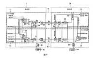
圖1係顯示例如對應於C-PHY規格或D-PHY規格之通信介面之通信系統之概要。圖1所示之通信系統具備:傳送部TX、與接收部RX。又,該通信系統具備:時脈通道CL,其橫跨傳送部TX與接收部RX,且傳輸時脈信號;與資料通道DL,其傳送例如圖像資料等之資料信號。另,於圖1中,作為資料通道DL,顯示具有4個資料通道DL1、DL2、DL3、DL4之例,但資料通道DL之數量不限定於此,例如可為僅1個資料通道DL1。Fig. 1 shows the outline of a communication system corresponding to the communication interface of the C-PHY specification or the D-PHY specification, for example. The communication system shown in Fig. 1 includes: a transmitting part TX and a receiving part RX. In addition, the communication system includes a clock channel CL, which straddles the transmitting part TX and the receiving part RX, and transmits clock signals, and a data channel DL, which transmits data signals such as image data. In addition, in FIG. 1, as the data channel DL, an example with 4 data channels DL1, DL2, DL3, DL4 is shown, but the number of data channels DL is not limited to this, for example, only one data channel DL1 can be used.
傳送部TX具有:傳送數位電路TX-DIGITAL、與傳送類比電路TX-ANALOG。於傳送數位電路TX-DIGITAL與傳送類比電路TX-ANALOG之間,傳輸例如16位元或8位元之並列信號。The transmission part TX has: a transmission digital circuit TX-DIGITAL, and a transmission analog circuit TX-ANALOG. Between the transmitting digital circuit TX-DIGITAL and the transmitting analog circuit TX-ANALOG, for example, 16-bit or 8-bit parallel signals are transmitted.
接收部RX具有:接收數位電路RX-DIGITAL、與接收類比電路RX-ANALOG。於資料通道DL1、DL2、DL3、DL4中,於接收類比電路RX-ANALOG與接收數位電路RX-DIGITAL之間,傳輸例如16位元或8位元之並列信號。於時脈通道CL中,於接收類比電路RX-ANALOG與接收數位電路RX-DIGITAL之間,傳輸例如2位元之串列信號。The receiving part RX has: receiving digital circuit RX-DIGITAL, and receiving analog circuitRX-ANALOG. In the data channels DL1, DL2, DL3, DL4, between the receiving analog circuit RX-ANALOG and the receiving digital circuit RX-DIGITAL, for example, 16-bit or 8-bit parallel signals are transmitted. In the clock channel CL, a 2-bit serial signal is transmitted between the receiving analog circuit RX-ANALOG and the receiving digital circuit RX-DIGITAL.
於時脈通道CL中,傳送類比電路TX-ANALOG與接收類比電路RX-ANALOG之間以傳輸差動之時脈信號之時脈信號線30連接。於資料通道DL1、DL2、DL3、DL4中,傳送類比電路TX-ANALOG與接收類比電路RX-ANALOG之間係以傳輸差動之資料信號之資料信號線31、32、33、34連接。時脈信號線30與資料信號線31、32、33、34分別具有傳輸差動信號之一對正信號線Dp與負信號線Dn。對時脈信號線30與資料信號線31、32、33、34分別傳輸例如2位元之串列信號。In the clock channel CL, the transmitting analog circuit TX-ANALOG and the receiving analog circuit RX-ANALOG are connected by a
圖2係顯示實現圖1所示之通信系統之比較例之通信系統之一構成例。另,於圖2中,作為圖1之資料通道DL,僅顯示1個資料通道DL1,但其他之資料通道DL2、DL3、DL4亦可為大致相同之構成。Fig. 2 shows a configuration example of a communication system that realizes the comparative example of the communication system shown in Fig. 1. In addition, in FIG. 2, as the data channel DL in FIG. 1, only one data channel DL1 is displayed, but the other data channels DL2, DL3, and DL4 can also have substantially the same structure.
該比較例之通信系統具備:傳送部101,其相當於圖1之傳送部TX;與接收部102,其相當於圖1之接收部RX。The communication system of this comparative example includes a
於時脈通道CL中,傳送部101具有:CL-HS電路111,其進行HS差動信號之處理;與CL-LP電路112,其進行LP信號之處理。於資料通道DL1中,傳送部101具有:DL-HS電路113,其進行HS差動信號之處理;與DL-LP電路114,其進行LP信號之處理。In the clock channel CL, the
於時脈通道CL中,接收部102具有:CL-HS電路121,其進行HS差動信號之處理;與CL-LP電路122,其進行LP信號之處理。於資料通道DL1中,接收部102具有:DL-HS電路123,其進行HS差動信號之處理;與DL-LP電路124,其進行LP信號之處理。In the clock channel CL, the receiving
圖3係顯示圖2所示之比較例之通信系統之具體電路構成例。又,圖4係顯示於圖2所示之比較例之通信系統中,傳輸至時脈通道CL與資料通道DL1之各個信號波形之一例。Fig. 3 shows a specific circuit configuration example of the communication system of the comparative example shown in Fig. 2.In addition, FIG. 4 shows an example of each signal waveform transmitted to the clock channel CL and the data channel DL1 in the communication system of the comparative example shown in FIG. 2.
如圖4所示,於該比較例之通信系統中,於時脈通道CL中,自傳送部101輸出至時脈信號線30之信號之狀態,存在成為以HS差動信號傳輸之狀態之HPS(High Speed State:高速狀態)期間、與成為以LP信號傳輸之狀態LPS(Low Power State:低功率狀態)期間。實質性的時脈信號於HPS期間以HS差動信號輸出。As shown in FIG. 4, in the communication system of the comparative example, in the clock channel CL, the state of the signal output from the
同樣地,於資料通道DL1中,自傳送部101輸出至資料信號線31之信號之狀態存在成為以HS差動信號傳輸之狀態之HPS期間、與成為以LP信號傳輸之狀態之LPS期間。實質性資料信號於HPS期間以HS差動信號輸出。另,於圖4中,將實質性資料信號部分記述為HST。又,於HPS期間,包含TRAIL期間THS-TRAIL及SYNC(同步)期間THS-SYNC等。不包含實質性資料信號部分之消隱期間包含於LPS期間。實質性資料信號例如以位元組單位輸出。Similarly, in the data channel DL1, the state of the signal output from the
如圖3所示,該通信系統具有:水晶振盪器(XTAL)82及PLL電路81,其向傳送部101內之各電路部供給時脈信號;與水晶振盪器(XTAL)83,其向接收部102內之各電路部供給時脈信號。As shown in FIG. 3, the communication system has: a crystal oscillator (XTAL) 82 and a
CL-HS電路111具有:HS狀態機(HS FSM)51、選擇器52、並列/串列(PS)轉換電路53、時脈分頻器(DIV)54、及HS驅動器(HS DRV)55。選擇器52選擇性輸出Toggle信號、值0之信號(ALL0)、與值1之信號(ALL1)。Toggle信號為例如8位元之時脈信號(1010_1010)。The CL-
CL-LP電路112具有:LP狀態機(LP FSM)41、LP編碼器(LP ENC)42、及LP驅動器(LP DRV)43。對LP狀態機41輸入時脈通道控制信號。The CL-
DL-HS電路113具有:HS狀態機(HS FSM)71、選擇器72、並列/串列(PS)轉換電路73、HS驅動器(HS DRV)74。自HS狀態機71輸出資料傳送準備完成信號TxReadyHS。選擇器72選擇性輸出傳送資料TxDataHS、同步編碼信號SYNC、值0之信號(ALL0)、及值1之信號(ALL1)。The DL-
DL-LP電路114具有:LP狀態機(LP FSM)61、LP編碼器(LP ENC)62、及LP驅動器(LP DRV)63。對LP狀態機61輸入資料傳送請求信號TxRequestHS。The DL-
另,於傳送部101中,LP驅動器43、HS驅動器55、LP驅動器63、及HS驅動器74相當於圖1之傳送類比電路TX-ANALOG。In addition, in the
CL-HS電路121具有:作為時脈信號終端電路之終端電路(TERM)56、HS接收器(HS RCV)57、及時脈分頻器(DIV)58。終端電路56具有終端電阻。The CL-
CL-LP電路122具有:LP接收器(LP RCV)44、LP解碼器(LP DEC)45、及LP狀態機(LP FSM)46。LP狀態機46輸出時脈通道CL之狀態信號。The CL-
DL-HS電路123具有:作為資料信號終端電路之終端電路(TERM)75、HS接收器(HS RCV)76、時脈分頻器(DIV)77、及字元對齊修正電路(ALN)78。終端電路75具有終端電阻。字元對齊修正電路(ALN)78輸出接收同步信號RxSyncHS、接收有效信號RxValidHS、及接收資料RxDataHS。The DL-
DL-LP電路124具有:LP接收器(LP RCV)64、LP解碼器(LP DEC)65、及LP狀態機(LP FSM)66。LP狀態機66輸出接收主動信號RxActiveHS。The DL-
另,於接收部102中,主要以LP接收器44、終端電路56、HS接收器57、LP接收器64、終端電路75、HS接收器76相當於圖1之接收類比電路RX-ANALOG。In addition, in the receiving
接著,就本揭示之第1實施形態進行說明。於以下,關於具有與上述比較例大致相同之構成及作用之部分,適當省略說明。Next, the first embodiment of the present disclosure will be described. In the following, descriptions of parts having substantially the same configuration and functions as those of the above-mentioned comparative example are appropriately omitted.
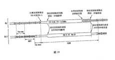
圖5係顯示實現圖1所示之通信系統之本揭示第1實施形態之通信系統之概要。圖6係顯示圖5所示之通信系統之具體電路構成例。又,圖7係顯示於圖5所示之通信系統中,傳輸至時脈通道CL與資料通道DL1之各個信號波形之一例。另,於圖5至圖7中,作為圖1之資料通道DL,僅顯示1個資料通道DL1,但其他之資料通道DL2、DL3、DL4亦可為大致相同之構成。Fig. 5 shows the outline of the communication system implementing the first embodiment of the present disclosure of the communication system shown in Fig. 1; Fig. 6 shows a specific circuit configuration example of the communication system shown in Fig. 5. In addition, FIG. 7 shows an example of each signal waveform transmitted to the clock channel CL and the data channel DL1 in the communication system shown in FIG. 5. In addition, in FIGS. 5 to 7, as the data channel DL in FIG. 1, only one data channel DL1 is shown, but the other data channels DL2, DL3, and DL4 can also have substantially the same structure.
本實施形態之通信系統具備:傳送部1(傳送裝置),其相當於圖1之傳送部TX;與接收部2(接收裝置),其相當於圖1之接收部RX。The communication system of this embodiment includes: a transmission unit 1 (transmission device), which corresponds to the transmission unit TX in FIG. 1, and a reception unit 2 (reception device), which corresponds to the reception unit RX in FIG. 1.
如圖7所示,於本實施形態之通信系統中,於時脈通道CL中,自傳送部1輸出至時脈信號線30之信號係於包括消隱期間在內全部為HS差動信號。如後述,於時脈通道CL中,於消隱期間,自傳送部1向時脈信號線30輸出特定之第1信號值(例如HS-0)之差動消隱信號、及與特定之第1信號值不同之特定第2信號值(例如HS-1)之差動信號,作為特定之消隱信號。As shown in FIG. 7, in the communication system of this embodiment, in the clock channel CL, the signal output from the
另,HS-0表示成為值0(差動0(差動-0))之差動信號,HS-1表示成為值1(差動1(差動-1))之差動信號。更具體而言,如圖8所示,HS-0之信號係指差動信號傳輸線之正信號線Dp之電壓位準為低、負信號線Dn之電壓位準為高之差動信號。又,HS-1之信號係指差動信號傳輸線之正信號線Dp之電壓位準為高、負信號線Dn之電壓位準為低之差動信號。In addition, HS-0 represents a differential signal that becomes a value of 0 (differential 0 (differential-0)), and HS-1 represents a differential signal that becomes a value of 1 (differential 1 (differential -1)). More specifically, as shown in FIG. 8, the signal of HS-0 refers to a differential signal in which the voltage level of the positive signal line Dp of the differential signal transmission line is low and the voltage level of the negative signal line Dn is high. In addition, the signal of HS-1 refers to a differential signal in which the voltage level of the positive signal line Dp of the differential signal transmission line is high and the voltage level of the negative signal line Dn is low.
同樣地,於資料通道DL1中,自傳送部1輸出至資料信號線31之信號,係包括消隱期間在內全部為HS差動信號。Similarly, in the data channel DL1, the signals output from the
另,於圖7中,將實質性資料信號的部分記述為HST。於實質性資料信號之前後期間亦可包含SYNC(同步)期間THS-SYNC與TRAIL期間THS-TRAIL。於資料通道DL1中,於消隱期間,可自傳送部1向資料信號線31於整個消隱期間輸出任意之差動信號(例如HS-0或HS-1),來作為特定之資料消隱信號。In addition, in FIG. 7, the part of the substantial data signal is described as HST. The period before and after the substantial data signal may also include a SYNC period THS-SYNC and a TRAIL period THS-TRAIL . In the data channel DL1, during the blanking period, any differential signal (such as HS-0 or HS-1) can be output from the
如圖6所示,本實施形態之通信系統具有:水晶振盪器(XTAL)82及PLL電路81,其向傳送部1內之各電路部供給時脈信號;及水晶振盪器(XTAL)83與PLL電路84,其向接收部2內之各電路部供給時脈信號。As shown in FIG. 6, the communication system of this embodiment has: a crystal oscillator (XTAL) 82 and a
於時脈通道CL中,傳送部1具有進行HS差動信號處理之CL-HS電路11。於資料通道DL1中,傳送部1具有進行HS差動信號處理之DL-HS電路13。In the clock channel CL, the
CL-HS電路11亦可為將包含差動之時脈信號之HS差動信號,輸出至時脈信號線30之差動時脈信號傳送電路。DL-HS電路13亦可為將差動之資料信號,輸出至資料信號線31之差動資料信號傳送電路。The CL-
於本實施形態之傳送部1中,可不包含相當於上述比較例之進行LP信號處理之CL-LP電路112及DL-LP電路114之電路。In the
CL-HS電路11如圖6所示,可具有與圖3之CL-HS電路111大致相同之電路。即,CL-HS電路11可具有:HS狀態機(HS FSM)51、選擇器52、並列/串列(PS)轉換電路53、時脈分頻器(DIV)54、及HS驅動器(HS DRV)55。選擇器52選擇性輸出Toggle信號、成為特定之第1信號值(HS-0)之值0之信號(ALL0)、及成為特定之第2信號值(HS-1)之值1之信號(ALL1)。Toggle信號為例如8位元之時脈信號(1010_1010)。於本實施形態中,將時脈通道控制信號與資料傳送請求信號TxRequestHS輸入HS狀態機51。As shown in FIG. 6, the CL-
DL-HS電路13如圖6所示,可具有與圖3之DL-HS電路113大致相同之電路。即,DL-HS電路13可具有:HS狀態機(HS FSM)71、選擇器72、並列/串列(PS)轉換電路73、HS驅動器(HS DRV)74。自HS狀態機71輸出資料傳送準備完成信號TxReadyHS。選擇器72選擇性輸出傳送資料TxDataHS、同步編碼信號SYNC、成為特定之第1信號值(HS-0)之值0之信號(ALL0)、及成為特定之第2信號值(HS-1)之值1之信號(ALL1)。The DL-
傳送部1具有消隱控制部20。如圖6所示,消隱控制部20可具有HS狀態機51與HS狀態機71。The
消隱控制部20係控制DL-HS電路13而與資料信號之消隱期間之開始時刻同步,自DL-HS電路13向資料信號線31取代資料信號而輸出特定之資料消隱信號。又,消隱控制部20係控制CL-HS電路11,而與資料信號之消隱期間之開始時刻同步地自CL-HS電路11向時脈信號線30取代時脈信號而輸出特定之第1信號值(例如HS-0)為遍及特定之期間以上連續之差動消隱信號。此處,特定之期間為長於時脈信號之時脈週期之期間。藉由將差動消隱信號設為特定之第1信號值為遍及長於時脈信號之時脈週期之期間連續之信號,於後述之接收部2之時脈狀態判別電路59中,可檢測信號之變化,且可檢測開始消隱期間。The blanking
又,消隱控制部20係控制CL-HS電路11,而與資料信號之消隱期間的結束時刻同步地自CL-HS電路11向時脈信號線30取代差動消隱信號而輸出與差動消隱信號不同之特定差動信號。具體而言,控制CL-HS電路11以輸出與特定之第1信號值不同之特定之第2信號值(例如HS-1)為遍及特定之期間以上連續的差動信號,作為特定之差動信號。另,可將以上說明之特定之第1信號值設為HS-1,將特定之第2信號值設為HS-0。藉由將特定之差動信號設為與特定之第1信號值不同之特定之第2信號值為遍及特定之期間以上連續的差動信號,於後述之接收部2之時脈狀態判別電路59中,可檢測信號之變化,可檢測消隱期間結束、資料信號之傳送。In addition, the blanking
於時脈通道CL中,接收部2具有進行HS差動信號處理之CL-HS電路21。於資料通道DL1中,接收部2具有進行HS差動信號處理之DL-HS電路23。In the clock channel CL, the receiving
DL-HS電路23可為經由資料信號線31接收差動之資料信號之差動資料信號接收電路。CL-HS電路21可為經由時脈信號線30接收差動之時脈信號、與自上述CL-HS電路11輸出之差動消隱信號之差動時脈信號接收電路。The DL-
於本實施形態之接收部2中,可不包含相當於上述比較例之進行LP信號處理之CL-LP電路122及DL-LP電路124之電路。In the receiving
DL-HS電路23如圖6所示,可包含與圖3之DL-HS電路123大致相同之電路。即,可具有:作為連接於資料信號線31之資料信號終端電路之終端電路(TERM)75、HS接收器(HS RCV)76、時脈分頻器(DIV)77、及字元對齊修正電路(ALN)78。終端電路75具有終端電阻。字元對齊修正電路(ALN)78係輸出接收同步信號RxSyncHS、接收有效信號RxValidHS、及接收資料RxDataHS。As shown in FIG. 6, the DL-
CL-HS電路21如圖6所示,具有與圖3之CL-HS電路121大致相同之電路。即,CL-HS電路21可具有:作為連接於時脈信號線30之時脈信號終端電路之終端電路(TERM)56、HS接收器(HS RCV)57、及時脈分頻器(DIV)58。終端電路56具有終端電阻。As shown in FIG. 6, the CL-
CL-HS電路21進而具有時脈(CL)狀態判別電路59。對時脈狀態判別電路59,經由HS接收器57輸入來自傳送部1之CL-HS電路11之時脈信號、特定之第1信號值(例如HS-0)之差動消隱信號(例如HS-0)、及特定之第2信號值(例如HS-1)之差動信號。The CL-
時脈狀態判別電路59具有作為終端控制電路之功能,且基於差動消隱信號,對資料信號終端電路(終端電路75)及時脈信號終端電路(終端電路56)進行使各者之終端電阻斷開之控制。又,時脈狀態判別電路59基於與資料信號之消隱期間之結束時刻同步輸出之特定之第2信號值(例如HS-1)的差動信號,對終端電路75及終端電路56進行使各者之終端電阻接通之控制。The clock
另,隨著終端電阻之接通/斷開,如圖7所示,時脈通道CL及資料通道DL1之消隱期間之信號之電壓振幅變化。又,藉由於消隱期間使終端控制斷開,可降低時脈信號線30及資料信號線31所流動之電流值。In addition, as the terminal resistance is turned on/off, as shown in FIG. 7, the voltage amplitude of the signal during the blanking period of the clock channel CL and the data channel DL1 changes. In addition, by turning off the terminal control due to the blanking period, the current value flowing in the
又,時脈狀態判別電路59具有輸出接收主動信號RxActiveHS而對字元對齊修正電路78進行字元對齊控制之功能。藉由於時脈狀態判別電路59中適當地檢測時脈消隱期間結束、且資料信號之傳送開始,可檢測同步編碼信號SYNC,並以字元對齊修正電路78適當地進行字元對齊控制。In addition, the clock
如以上,根據本實施形態,由於與資料信號之消隱期間之開始時刻同步地向時脈信號線30取代時脈信號而輸出特定之第1信號值為遍及特定之期間以上連續之差動消隱信號,故可謀求資料傳輸時之低消耗電力化。As described above, according to the present embodiment, since the
又,由於經由時脈信號線30接受差動之時脈信號、及與資料信號之消隱期間之開始時刻同步且以特定之第1信號值為遍及特定之期間以上連續之方式輸出的差動消隱信號,故可謀求資料傳輸時之低消耗電力化。In addition, because the differential clock signal is received via the
又,根據本實施形態,在上述比較例之通信系統中未被有效運用之LP信號部分(消隱期間)亦可傳送利用HS差動信號輸出之資料信號,可降低利用HS差動輸出之資料信號之傳輸率,實現整體低消耗電力化。又,根據本實施形態,與上述比較例之通信系統相比,不需要進行LP信號之處理,故可削減電路規模。In addition, according to this embodiment, the part of the LP signal (blanking period) that is not effectively used in the communication system of the above-mentioned comparative example can also transmit the data signal output using the HS differential signal, which can reduce the data output using the HS differential signal. The signal transmission rate achieves overall low power consumption. Furthermore, according to the present embodiment, compared with the communication system of the above-mentioned comparative example, LP signal processing is not required, so the circuit scale can be reduced.
另,本說明書記載之效果僅為例示並非限定者,亦可有其他之效果。關於以下其他之實施形態之效果亦相同。In addition, the effects described in this manual are merely illustrative and not limiting, and other effects are also possibleeffect. The effects of the following other embodiments are the same.
接著,就本揭示之第2實施形態進行說明。以下對於具有與上述比較例、上述第1實施形態大致相同之構成及作用之部分,適當省略說明。Next, the second embodiment of the present disclosure will be described. Hereinafter, descriptions of parts having substantially the same configuration and functions as the above-mentioned comparative example and the above-mentioned first embodiment will be omitted as appropriate.
圖9係顯示本實施形態之通信系統之具體電路構成例。又,圖10係顯示於本實施形態之通信系統中傳輸至時脈通道CL與資料通道DL1之各個信號波形之一例。另,於圖9及圖10中,作為圖1之資料通道DL,僅顯示1個資料通道DL1,但其他之資料通道DL2、DL3、DL4亦可為大致相同之構成。另,顯示本實施形態之通信系統概要之區塊構成可與圖5大致相同。Fig. 9 shows a specific circuit configuration example of the communication system of this embodiment. In addition, FIG. 10 shows an example of each signal waveform transmitted to the clock channel CL and the data channel DL1 in the communication system of this embodiment. In addition, in FIG. 9 and FIG. 10, as the data channel DL in FIG. 1, only one data channel DL1 is shown, but other data channels DL2, DL3, and DL4 can also have substantially the same structure. In addition, the block structure showing the outline of the communication system of this embodiment can be substantially the same as that shown in FIG. 5.
於本實施形態中,亦與上述第1實施形態相同,消隱控制部20係控制CL-HS電路11,而與資料信號之消隱期間之結束時刻同步地自CL-HS電路11向時脈信號線30取代差動消隱信號而輸出與差動消隱信號不同之特定之差動信號。於上述第1實施形態中,控制CL-HS電路11以輸出特定之第2信號值(例如HS-1)為遍及特定之期間以上連續的差動信號,作為特定之差動信號。相對於此,於本實施形態中,控制CL-HS電路11以遍及特定之期間以上輸出時脈信號,作為特定之差動信號。藉由將特定之差動信號設為遍及特定之期間以上之時脈信號,可於接收部2A之時脈狀態判別電路59中,檢測信號之變化,且可檢測消隱期間結束、資料信號之傳送開始。In this embodiment, as in the above-mentioned first embodiment, the blanking
於本實施形態中,如圖7所示,於時脈通道CL中,於消隱期間,自傳送部1向時脈信號線30輸出特定之第1信號值(例如HS-0或HS-1)之差動消隱信號、與時脈信號。In this embodiment, as shown in FIG. 7, in the clock channel CL, during the blanking period, the
與圖6之電路構成相比,於圖9之電路中,輸入於接收部2A之CL-HS電路21之時脈狀態判別電路59之信號不同。即,於圖6之電路構成之接收部2中,對時脈狀態判別電路59,直接輸入來自HS接收器57之信號。相對於此,於圖9之電路構成之接收部2A中,對時脈狀態判別電路59,不直接輸入來自HS接收器57之信號,而輸入以時脈分頻器58分頻之信號。藉此,檢測消隱期間之開始時刻及結束時刻。Compared with the circuit configuration of FIG. 6, in the circuit of FIG. 9, the signal of the clock
其他之構成及動作可與上述第1實施形態之通信系統大致相同。The other configuration and operation can be substantially the same as the communication system of the first embodiment described above.
接著,就第2實施形態之通信系統之第1至第5變化例進行說明。Next, the first to fifth modified examples of the communication system of the second embodiment will be described.
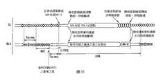
圖11~圖15係顯示第1至第5變化例之通信系統中傳輸至時脈通道CL與資料通道DL1之各個信號波形之一例。另,於圖11~圖15中,作為圖1之資料通道DL,僅顯示1個資料通道DL1,但其他之資料通道DL2、DL3、DL4亦可大致相同。又,表示本實施形態之通信系統概要之區塊構成可與圖5大致相同。Figures 11 to 15 show an example of each signal waveform transmitted to the clock channel CL and the data channel DL1 in the communication system of the first to fifth variations. In addition, in FIGS. 11-15, as the data channel DL in FIG. 1, only one data channel DL1 is displayed, but the other data channels DL2, DL3, and DL4 can be roughly the same. In addition, the block structure showing the outline of the communication system of this embodiment can be substantially the same as in FIG. 5.
於圖11所示之第1變化例中,相對於圖10所示之例,於消隱期間自傳送部1輸出至資料通道DL1之信號不同。於資料通道DL1中,於消隱期間,自傳送部1之DL-HS電路13,首先輸出於HST期間傳輸之實質性資料信號最後之值之反相值的差動信號,作為特定之資料消隱信號。其後,自DL-HS電路13輸出差動0(HS-0)之差動信號。In the first modification example shown in FIG. 11, compared with the example shown in FIG. 10, the signal output from the
消隱控制部20係控制DL-HS電路13,而與消隱期間之開始時刻同步地自DL-HS電路13向資料信號線31輸出資料信號的最後之值之反相值之差動信號。又,消隱控制部20係控制DL-HS電路13,而與消隱期間之結束時刻同步地取代資料信號最後之值之反相值之差動信號,而自DL-HS電路13向資料信號線31輸出HS-0之差動信號。另,對時脈信號線30,與圖10之例相同,與消隱期間之結束時刻同步,自傳送部1之CL-HS電路11向時脈信號線30遍及特定之期間以上輸出時脈信號。於消隱期間輸出之HS-0之差動信號與時脈信號之各個輸出的開始時刻可不同。The blanking
根據該第1變化例,藉由將資料通道DL1之消隱期間之最後期間設為HS-0之差動信號,消隱期間之最後期間之信號值、與接下來之SYNC(同步)期間THS-SYNC的開始時之信號值為相同值,可使接收側之同步處理變得容易。又,一般,資料通道DL1之TRAIL期間THS-TRAIL之信號成為資料信號的最後之值之反相值之差動信號。因此,根據該第1變化例,可將消隱期間開始時之信號值合併為TRAIL期間THS-TRAIL之信號。According to the first modification example, by setting the last period of the blanking period of the data channel DL1 as the differential signal of HS-0, the signal value of the last period of the blanking period and the subsequent SYNC (synchronization) period T The signal value at the beginning ofHS-SYNC is the same value, which makes the synchronization process on the receiving side easier. Also, generally, the signal of THS- TRAIL during the TRAIL period of the data channel DL1 becomes a differential signal of the inverted value of the final value of the data signal. Therefore, according to the first modification, the signal value at the beginning of the blanking period can be combined into the signal of THS-TRAIL during the TRAIL period.
其他可與圖10之信號波形大致相同。Others can be roughly the same as the signal waveform in FIG. 10.
於圖12所示之第2變化例中,相對於圖11所示之第1變化例,自傳送部1之CL-HS電路11輸出至時脈信號線30之信號有部分不同。於時脈通道CL中,於消隱期間,自傳送部1之CL-HS電路11,首先,與圖7所示之上述第1實施形態同樣地輸出特定之第1信號值(例如HS-0或HS-1)之差動信號。其後,與上述第1實施形態相同,自CL-HS電路11,輸出與特定之第1信號值不同之特定之第2信號值(例如HS-1或HS-0)之差動信號。其後,經過使終端電阻接通之時刻後,自CL-HS電路11輸出時脈信號。在自CL-HS電路11輸出特定之第2信號值之差動信號後,隔著使終端電阻接通之時刻,接著輸出時脈信號,此點與上述第1實施形態不同。消隱控制部20係控制CL-HS電路11以自CL-HS電路11在適當之時序輸出差動信號與時脈信號。In the second modification example shown in FIG. 12, compared to the first modification example shown in FIG. 11, the signal output from the CL-
根據該第2變化例,與如第1變化例於時脈信號之輸出期間中使終端電阻接通之情形相比,可降低因時脈通道CL之終端電阻斷開時之時脈信號之反射引起之波形混亂的影響。According to the second modification example, compared with the case where the terminal resistance is turned on during the output period of the clock signal as in the first modification example, the reflection of the clock signal when the terminal resistance of the clock channel CL is turned off can be reduced The impact of the chaotic waveform caused.
其他可於圖11之第1變化例大致相同。Others can be roughly the same as in the first modification of FIG. 11.
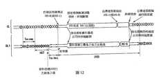
於圖13所示之第3變化例中,相對於圖12所示之第2變化例,於消隱期間自傳送部1輸出至資料通道DL1之信號不同。於該第3變化例中,遍及整個消隱期間,自傳送部1之DL-HS電路13輸出HS-0之差動信號,作為特定之資料消隱信號。消隱控制部20係控制DL-HS電路13以自DL-HS電路13在適當之時序輸出HS-0之差動信號。In the third modification example shown in FIG. 13, compared to the second modification example shown in FIG. 12, the signal output from the
其他可於圖12之第2變化例大致相同。Others can be roughly the same as in the second modification of FIG. 12.
於圖14所示之第4變化例中,相對於圖11所示之第1變化例,於消隱期間自傳送部1輸出至資料通道DL1之信號有部分不同。於該第4變化例中,於資料通道DL1中,於消隱期間,自傳送部1之DL-HS電路13,首先輸出HS-1之差動信號作為特定之資料消隱信號。其後,自DL-HS電路13輸出HS-0之差動信號。消隱控制部20係控制DL-HS電路13以自DL-HS電路13在適當之時序輸出HS-1之差動信號與HS-0之差動信號。In the fourth modification example shown in FIG. 14, compared to the first modification example shown in FIG. 11, the signal output from the
其他可於圖11之第1變化例大致相同。Others can be roughly the same as in the first modification of FIG. 11.
於圖15所示之第5變化例中,相對於圖12所示之第2變化例,於消隱期間自傳送部1輸出至資料通道DL1之信號有部分不同。於該第5變化例中,於資料通道DL1中,於消隱期間,自傳送部1之DL-HS電路13,首先,輸出HS-1之差動信號作為特定之資料消隱信號。其後,自DL-HS電路13輸出HS-0之差動信號。消隱控制部20係控制DL-HS電路13以自DL-HS電路13在適當之時序輸出HS-1之差動信號與HS-0之差動信號。In the fifth modification shown in FIG. 15, compared with the second modification shown in FIG. 12, the signal output from the
其他可與圖12之第2變化例大致相同。Others can be roughly the same as the second modification example in FIG. 12.
接著,就本揭示之第3實施形態進行說明。以下對於具有與上述比較例、上述第1實施形態或上述第2實施形態大致相同之構成及作用之部分,適當省略說明。Next, the third embodiment of the present disclosure will be described. The following is the same as the aboveIn the comparative example, the above-mentioned first embodiment, or the above-mentioned second embodiment, which have substantially the same structure and function, the description is appropriately omitted.
圖16係顯示本揭示第3實施形態之通信系統之概要。本實施形態之通信系統具備:相當於圖1之傳送部TX之傳送部1B(傳送裝置)、與相當於圖1之接收部RX之接收部2B(接收裝置)。Fig. 16 shows the outline of the communication system of the third embodiment of the present disclosure. The communication system of this embodiment includes a
於上述第1及第2實施形態之通信系統中,將時脈通道CL與資料通道DL1各者中傳送之信號於包括消隱期間在內全部設為HS差動信號。相對於此,本實施形態之通信系統設為具備亦可進行利用LP信號通信之切換電路,且可切換不使用LP信號而僅以HS差動信號進行通信之模式、與使用LP信號與HS差動信號兩者進行通信之模式者。In the communication systems of the first and second embodiments described above, the signals transmitted in each of the clock channel CL and the data channel DL1 are all HS differential signals including the blanking period. In contrast, the communication system of this embodiment is equipped with a switching circuit that can also communicate using LP signals, and can switch the mode of communication using only HS differential signals without using LP signals, which is different from using LP signals and HS. A mode in which the two signals communicate with each other.
於本實施形態之通信系統中,傳送部1B具有實現與上述第1及第2實施形態之通信系統大致相同功能之消隱控制部20。In the communication system of this embodiment, the
又,傳送部1B係於時脈通道CL中具有:進行HS差動信號處理之CL-HS電路11、進行LP信號處理之CL-LP電路12、切換開關15、及選擇器17。In addition, the
CL-LP電路12可為輸出第1單端信號作為LP信號之第1單端信號傳送電路。CL-LP電路12可為具有與圖2之CL-LP電路112大致相同功能者。切換開關15可為切換信號輸出之路徑以自CL-HS電路11與CL-LP電路12中之任一者向時脈信號線30進行信號輸出之第1傳送切換電路。選擇器17為如下之電路:於不使用LP信號而僅以HS差動信號進行通信之模式中,將來自消隱控制部20之控制信號輸入至CL-HS電路11,於使用LP信號與HS差動信號兩者進行通信之模式中,不將來自消隱控制部20之控制信號輸出至CL-HS電路11。The CL-
又,傳送部1B具有:於資料通道DL1中進行HS差動信號處理之DL-HS電路13、進行LP信號處理之DL-LP電路14、切換開關16、及選擇器18。In addition, the
DL-LP電路14可為輸出第2單端信號作為LP信號之第2單端信號傳送電路。DL-LP電路14可為具有與圖2之DL-LP電路114大致相同功能者。切換開關16可為切換信號輸出之路徑以自DL-HS電路13與DL-LP電路14中之任一者向資料信號線31進行信號輸出之第2傳送切換電路。選擇器18為如下之電路:於不使用LP信號而僅以HS差動信號進行通信之模式中,將來自消隱控制部20之控制信號輸入至DL-HS電路13,於使用LP信號與HS差動信號兩者進行通信之模式中,不將來自消隱控制部20之控制信號輸出至DL-HS電路13。The DL-
接收部2B具有:於時脈通道CL中進行HS差動信號處理之CL-HS電路21、進行LP信號處理之CL-LP電路22、選擇器25、選擇器27、及選擇器28。CL-LP電路22可為經由時脈信號線30接收第1單端信號作為LP信號之第1單端信號接收電路。CL-LP電路22可為具有與圖2之CL-LP電路122大致相同功能者。The receiving
選擇器25可為切換是否接收第1單端信號作為LP信號之第1接收切換電路。選擇器25為如下之電路:於不使用LP信號而僅以HS差動信號進行通信之模式中,不將經由時脈信號線30接收到之信號輸入至CL-LP電路22,於使用LP信號與HS差動信號兩者進行通信之模式中,將經由時脈信號線30接收到之信號輸入至CL-LP電路22。選擇器27為如下之電路:於不使用LP信號而僅以HS差動信號進行通信之模式中,將來自CL-HS電路21之終端控制信號輸入至DL-HS電路23;於使用LP信號與HS差動信號兩者進行通信之模式中,不輸入來自HS電路21之終端控制信號。選擇器28為如下之電路:於不使用LP信號而僅以HS差動信號進行通信之模式中,將來自CL-HS電路21之字元對齊控制信號輸入至DL-HS電路23;於使用LP信號與HS差動信號兩者進行通信之模式中,不輸入來自HS電路21之字元對齊控制信號。The
又,接收部2B係於資料通道DL1中具有:進行HS差動信號處理之DL-HS電路23、進行LP信號處理之DL-LP電路24、及選擇器26。DL-LP電路24可為經由資料信號線31接收第2單端信號作為LP信號之第2單端信號接收電路。In addition, the receiving
選擇器26可為切換是否接收第2單端信號作為LP信號之第2接收切換電路。選擇器26為如下之電路:於不使用LP信號而僅以HS差動信號進行通信之模式中,不將經由資料信號線31接收到之信號輸入至DL-LP電路24;於使用LP信號與HS差動信號兩者進行通信之模式中,將經由資料信號線31接收到之信號輸入至DL-LP電路24。The
圖17係顯示本實施形態之通信系統之具體應用例。Fig. 17 shows a specific application example of the communication system of this embodiment.
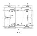
例如,本實施形態之通信系統如圖17所示,可應用於自影像感測器IS向應用處理器AP之資料傳輸。傳送部1B設置於影像感測器IS內。接收部2B設置於應用處理器AP內。影像感測器IS與應用處理器AP之間,藉由時脈信號線30與資料信號線31連接。時脈信號線30與資料信號線31之信號傳輸為單一方向。For example, the communication system of this embodiment is shown in FIG. 17, and can be applied to data transmission from the image sensor IS to the application processor AP. The
又,影像感測器IS與應用處理器AP之間,藉由雙向之控制匯流排35連接。控制匯流排35可使用I2C(Inter-Intergrated Circuit:內部積體電路)介面或其擴展版即I3C介面。In addition, the image sensor IS and the application processor AP are connected by a
圖18係顯示包含圖17所示之影像感測器IS及應用處理器AP之機器之資料傳送處理的一例。FIG. 18 shows an example of data transmission processing of a machine including the image sensor IS and the application processor AP shown in FIG. 17.
包含影像感測器IS及應用處理器AP之機器一經投入電源(步驟S101),應用處理器AP便使用控制匯流排35,讀入影像感測器IS之暫存器設定(步驟S102)。藉此,應用處理器AP判斷影像感測器IS是否支援無LP信號之通信(步驟S103)。即,判斷是否支援以下任一者模式:不使用LP信號而僅以HS差動信號進行通信之模式、及使用LP信號與HS差動信號兩者進行通信之模式。Once the machine including the image sensor IS and the application processor AP is powered on (step S101), the application processor AP uses the
於判斷為支援無LP信號之通信之情形時(步驟S103:是),應用處理器AP使用控制匯流排35,將啟用無LP信號之通信之設定傳送至影像感測器IS(步驟S104)。接著,應用處理器AP使用控制匯流排35,向影像感測器IS輸出傳送開始指示之信號(步驟S105)。於判斷為不支援無LP信號之通信之情形(步驟S103:否)時,應用處理器AP視為使用LP信號與HS差動信號兩者進行通信之模式,使用控制匯流排35,向影像感測器IS輸出傳送開始指示之信號(步驟S105)。接著,影像感測器IS接收傳送開始指示之信號,開始資料信號之傳送(步驟S106)。When it is determined that the communication without LP signal is supported (step S103: Yes), the applicationThe processor AP uses the
接著,就本揭示之第4實施形態進行說明。以下對於具有與上述比較例、或上述第1至第3實施形態大致相同之構成及作用之部分,適當省略說明。Next, the fourth embodiment of the present disclosure will be described. Hereinafter, descriptions of parts having substantially the same structure and function as the above-mentioned comparative example or the above-mentioned first to third embodiments will be omitted as appropriate.
圖19係顯示本揭示第4實施形態之通信系統之概要。圖20係顯示於本實施形態之通信系統中於時脈通道CL與資料通道DL1中傳輸之各個信號波形之第1例。圖21係顯示於本實施形態之通信系統中於時脈通道CL與資料通道DL1中傳輸之各個信號波形之第2例。另,於圖19至圖21中,作為圖1之資料通道DL,僅顯示1個資料通道DL1,但其他之資料通道DL2、DL3、DL4亦可為大致相同之構成。Fig. 19 shows the outline of the communication system of the fourth embodiment of the present disclosure. FIG. 20 shows a first example of each signal waveform transmitted in the clock channel CL and the data channel DL1 in the communication system of this embodiment. FIG. 21 shows a second example of each signal waveform transmitted in the clock channel CL and the data channel DL1 in the communication system of this embodiment. In addition, in FIGS. 19-21, as the data channel DL of FIG. 1, only one data channel DL1 is shown, but the other data channels DL2, DL3, and DL4 may also have substantially the same structure.
本實施形態之通信系統相對於圖5所示之通信系統之構成,其終端控制的部分不同。於上述第1至第3實施形態中,於消隱期間,進行終端電阻之接通/斷開控制,但於本實施形態中,省略該終端電阻之接通/斷開控制。The communication system of this embodiment differs from the configuration of the communication system shown in FIG. 5 in terms of terminal control. In the above-mentioned first to third embodiments, the on/off control of the terminating resistor is performed during the blanking period, but in this embodiment, the on/off control of the terminating resistor is omitted.
於圖20之第1例中,顯示將時脈通道CL與資料通道DL1之終端電阻設為始終接通之狀態之情形之例。於圖20之第1例之情形,可設置可切換接通/斷開之終端電阻,並將終端電阻設為始終接通之狀態,亦可設置始終接通之固定終端電阻。In the first example in FIG. 20, an example is shown in which the terminal resistances of the clock channel CL and the data channel DL1 are always on. In the case of the first example in Fig. 20, a terminal resistance that can be switched on/off can be set, and the terminal resistance can be set to always on, or a fixed terminal resistor that is always on can be set.
又,於圖21之第2例中,顯示將時脈通道CL與資料通道DL1之終端電阻設為始終斷開之狀態之情形之例。於圖21之第2例之情形,可省略終端電阻本身,亦可設置可切換接通/斷開之終端電阻,並將終端電阻設為始終斷開之狀態。Also, in the second example of Figure 21, it is shown that the end of the clock channel CL and the data channel DL1This is an example of the case where the terminal resistance is set to always be off. In the case of the second example in Figure 21, the terminal resistor itself can be omitted, and a terminal resistor that can be switched on/off can also be set, and the terminal resistor can be set to always be off.
於圖20之第1例與圖21之第2例中,信號之電壓振幅不同。於將終端電阻設為接通之情形時,與將終端電阻設為斷開之情形相比,電壓振幅減小。因此,圖20之第1例之電壓振動小於圖21之第2例之電壓振動。In the first example of FIG. 20 and the second example of FIG. 21, the voltage amplitude of the signal is different. When the terminal resistance is set to ON, the voltage amplitude decreases compared with the case where the terminal resistance is set to OFF. Therefore, the voltage vibration of the first example of FIG. 20 is smaller than that of the second example of FIG. 21.
其他可與圖11之信號波形大致相同。Others can be roughly the same as the signal waveform in FIG. 11.
接著,就上述各實施形態說明之通信系統之應用例進行說明。Next, an application example of the communication system described in the above embodiments will be described.
圖22係表示應用上述各實施形態之通信系統之智慧型手機300(多功能行動電話)之外觀者。於該智慧型手機300中搭載有各種裝置,於該等裝置間進行資料交換之通信系統中,應用上述各實施形態之通信系統。FIG. 22 shows the appearance of a smart phone 300 (multifunctional mobile phone) to which the communication system of each of the above embodiments is applied. Various devices are mounted in the
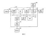
圖23係表示使用於智慧型手機300之應用處理器310之一構成例者。應用處理器310具有:CPU(Central Processing Unit:中央處理單元)311、記憶體控制部312、電源控制部313、外部介面部314、GPU(Graphics Processing Unit:圖形處理單元)315、媒體處理部316、顯示器控制部317、及MIPI介面部318。CPU311、記憶體控制部312、電源控制部313、外部介面部314、GPU315、媒體處理部316、顯示器控制部317於該例中,連接於系統匯流排319,並經由該系統匯流排319可彼此進行資料之交換。FIG. 23 shows an example of the configuration of the
CPU311為按照程式而處理智慧型手機300中操作之各種資訊者。記憶體控制部312為控制CPU311進行資訊處理時所使用之記憶體501者。電源控制部313為控制智慧型手機300之電源者。The
外部介面部314為用以與外部裝置通信之介面,於該例中,與無線通信部502及影像感測器410連接。無線通信部502為與行動電話之基地台進行無線通信者,例如包含基頻部、或RF(Radio Frequency:射頻)前端部等而構成。影像感測器410為取得圖像者,例如包含CMOS感測器而構成。The
GPU315為進行圖像處理者。媒體處理部316為處理語音、文字、或圖形等資訊者。顯示器控制部317為經由MIPI介面318而控制顯示器504者。GPU315 is an image processor. The
MIPI介面318為將圖像信號傳送至顯示器504者。作為圖像信號,例如可使用YUV形式或RGB形式等信號。對該MIPI介面318與顯示器504之間之通信系統,例如應用上述各實施形態之通信系統。The
圖24係表示影像感測器410之一構成例者。影像感測器410具有:感測器部411、ISP(Image Signal Processor:影像信號處理器)412、JPEG(Joint Pgotographic Experts Group:聯合圖像專家組)編碼部413、CPU414、RAM(Random Access Memory:隨機存取記憶體)415、ROM(Read Only Memory:唯讀記憶體)416、電源控制部417、I2C(Inter-Intergrated Circuit:內部積體電路)介面418、及MIPI介面419。該等各區塊於該例中連接於系統匯流排420,並經由該系統匯流排420,彼此可進行資料之交換。FIG. 24 shows an example of the configuration of the
感測器部411為取得圖像者,且為例如藉由CMOS感測器構成者。ISP412為對感測器部411取得之圖像進行特定之處理者。JPEG編碼器413為編碼ISP412處理之圖像並產生JPEG形式之圖像者。CPU414為按照程式而控制影像感測器410之各區塊者。RAM15為CPU414進行資訊處理時所使用之記憶體。ROM416為記憶CPU414中執行之程式者。電源控制部417為控制影像感測器410之電源者。I2C介面418為自應用處理器310接收控制信號者。又,雖未圖示,但影像感測器410自應用處理器310除了接收控制信號以外亦接收時脈信號。具體而言,影像感測器410構成為可基於各種頻率之時脈信號動作。The
MIPI介面419為將圖像信號傳送至應用處理器310者。例如可使用YUV格式或RGB格式等之信號作為圖像信號。對該MIPI介面419與應用處理器310之間之通信系統,例如應用上述各實施形態之通信系統。The
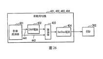
於圖25及圖26,作為攝像裝置之應用例,顯示車載用相機之構成例。圖25係顯示車載用相機之設置例之一例,圖26係顯示車載用相機之內部構成例。25 and 26, as an application example of the imaging device, a configuration example of an in-vehicle camera is shown. Fig. 25 shows an example of the installation of an in-vehicle camera, and Fig. 26 shows an example of the internal structure of an in-vehicle camera.
例如,如圖25所示,於車輛301之前方(front)設置車載用相機401,於左右設置車載用相機402、403,進而於後方(rear)設置車載用相機404。車載用相機401~404分別經由車內網路而連接於ECU302(Electrical Control Unit:電子控制單元)。For example, as shown in FIG. 25, an in-
車輛301之前方所具備之車載用相機401之圖像獲取角度例如為於圖25以a所示之範圍。車載用相機402之圖像獲取角度例如為於圖25以b所示之方式。車載用相機403之圖像獲取角度例如為於圖25以c所示之範圍。車載用相機404之圖像獲取角度例如為於圖25以d所示之範圍。車載用相機401~404分別將獲取之圖像輸出至ECU302。其結果,可於ECU302中獲取車輛301之前方、左右、後方之360度(全方位)之圖像。The image acquisition angle of the in-
例如,如圖26所示,車載用相機401~404分別具有:影像感測器431、DSP(Digital Signal Processing:數位信號處理)電路432、選擇器433、及SerDes(SERializer/DESerializer:串連器/解串器)電路444。For example, as shown in FIG. 26, the in-
DSP電路432為對自影像感測器431輸出之攝像信號進行各種圖像信號處理者。SerDes電路444為進行信號之串列/並列轉換者,例如以FPD-LinkIII等車載介面晶片構成。The
選擇器433為選擇將自影像感測器431輸出之攝像信號經由DSP電路432輸出、或不經由DSP電路432輸出者。The
於影像感測器431與DSP電路432間之連接介面441,例如可應用上述各實施形態之通信系統。又,於影像感測器431與選擇器433間之連接介面442,例如可應用上述各實施形態之通信系統。For the
本揭示之技術不限定於上述各實施形態之說明而可有各種變化實施。The technology of the present disclosure is not limited to the description of each of the above-mentioned embodiments and can be implemented with various changes.
例如,本技術可採用以下之構成。For example, this technology can adopt the following configurations.
(1)(1)
一種傳送裝置,其具備:時脈信號傳送電路,其將時脈信號輸出至時脈信號線;資料信號傳送電路,其將資料信號傳送於資料信號線;及消隱控制部,其控制上述時脈信號傳送電路,而與上述資料信號之消隱期間同步地自上述時脈信號傳送電路向上述時脈信號線取代上述時脈信號而輸出特定之消隱信號。A transmission device comprising: a clock signal transmission circuit which outputs the clock signal to the clock signal line; a data signal transmission circuit which transmits the data signal to the data signal line; and a blanking control section which controls the aforementioned time A pulse signal transmission circuit is synchronized with the blanking period of the data signal from the clock signal transmission circuit to the clock signal line to replace the clock signal and output a specific blanking signal.
(2)(2)
如(1)自傳送裝置,其中上述時脈信號傳送電路係將差動之時脈信號作為上述時脈信號而輸出至上述時脈信號線之差動時脈信號傳送電路,上述資料信號傳送電路係將差動之資料信號作為上述資料信號而輸出至上述資料信號線之差動資料信號傳送電路,上述消隱控制部係控制上述差動時脈信號傳送電路,而與上述資料信號之消隱期間之開始時刻同步地,自上述差動時脈信號傳送電路向上述時脈信號線輸出特定之第1信號值為遍及特定之期間以上連續之差動消隱信號,作為特定之消隱信號。Such as (1) a self-transmitting device, wherein the clock signal transmission circuit outputs a differential clock signal as the clock signal to the differential clock signal transmission circuit of the clock signal line, and the data signal transmission circuit The differential data signal is output to the differential data signal transmission circuit of the data signal line as the data signal, and the blanking control section controls the differential clock signal transmission circuit to be blanked with the data signal Synchronously at the beginning of the period, the differential clock signal transmission circuit outputs a specific first signal value to the clock signal line over the specific period.The continuous differential blanking signal is used as a specific blanking signal.
(3)(3)
如(2)之傳送裝置,其中上述特定之期間係長於上述時脈信號之時脈週期之期間。Such as the transmission device of (2), wherein the specific period is longer than the period of the clock cycle of the clock signal.
(4)(4)
如(2)或(3)之傳送裝置,其中上述消隱控制部係控制上述差動時脈信號傳送電路,而與上述資料信號之消隱期間之結束時刻同步地,自上述差動時脈信號傳送電路向上述時脈信號線取代上述差動消隱信號而輸出與上述差動消隱信號不同之特定之差動信號。Such as the transmission device of (2) or (3), wherein the blanking control unit controls the differential clock signal transmission circuit, and is synchronized with the end time of the blanking period of the data signal from the differential clock The signal transmission circuit replaces the differential blanking signal to the clock signal line and outputs a specific differential signal different from the differential blanking signal.
(5)(5)
如(4)之傳送裝置,其中上述消隱控制部係控制上述差動時脈信號傳送電路,而自上述差動時脈信號傳送電路向上述時脈信號線,輸出與上述特定之第1信號值不同之特定之第2信號值為遍及上述特定之期間以上連續的差動信號,作為上述特定之差動信號。Such as the transmission device of (4), wherein the blanking control unit controls the differential clock signal transmission circuit, and the differential clock signal transmission circuit outputs the specific first signal to the clock signal line The specific second signal value with a different value is a differential signal that is continuous over the specific period or more, and is used as the specific differential signal.
(6)(6)
如(4)之傳送裝置,其中上述消隱控制部係控制上述差動時脈信號傳送電路,而自上述差動時脈信號傳送電路向上述時脈信號線遍及上述特定之期間以上輸出上述時脈信號,作為上述特定之差動信號。Such as the transmission device of (4), wherein the blanking control unit controls the differential clock signal transmission circuit, and the differential clock signal transmission circuit outputs the clock signal to the clock signal line over the specified period of time. The pulse signal is used as the above-mentioned specific differential signal.
(7)(7)
如(5)之傳送裝置,其中上述消隱控制部係控制上述差動時脈信號傳送電路,而於輸出上述特定之第2信號值之信號後,於上述消隱期間內自上述差動時脈信號傳送電路向上述時脈信號線輸出上述時脈信號。Such as the transmission device of (5), wherein the blanking control unit controls the differential clock signal transmission circuit, and after outputting the signal of the specific second signal value, it starts from the differential time during the blanking period The pulse signal transmission circuit outputs the clock signal to the clock signal line.
(8)(8)
如(2)至(7)中任一項之傳送裝置,其中上述消隱控制部進而控制上述資料信號傳送電路,而與上述資料信號之消隱期間之開始時刻同步地,自上述資料信號傳送電路向上述資料信號線取代上述資料信號而至少輸出特定之資料消隱信號。Such as the transmission device of any one of (2) to (7), wherein the blanking control unit further controls the data signal transmission circuit, and is synchronized with the start time of the blanking period of the data signal to transmit from the data signal The circuit replaces the data signal to the data signal line and outputs at least a specific data blanking signal.
(9)(9)
如(8)之傳送裝置,其中上述消隱控制部係控制上述資料信號傳送電路,而輸出將上述資料信號之最後之信號值反轉後之信號作為上述特定之資料消隱信號。Such as the transmission device of (8), wherein the blanking control unit controls the data signal transmission circuit, and outputs a signal after inverting the last signal value of the data signal as the specific data blanking signal.
(10)(10)
如(8)之傳送裝置,其中上述消隱控制部係控制上述差動資料信號傳送電路,而輸出值為1之差動信號作為上述特定之資料消隱信號。Such as the transmission device of (8), wherein the blanking control unit controls the differential data signal transmission circuit, and outputs a differential signal with a value of 1 as the specific data blanking signal.
(11)(11)
如(8)之傳送裝置,其中上述消隱控制部係控制上述差動資料信號傳送電路,而於輸出上述特定之資料消隱信號後,與上述資料信號之消隱期間之結束時刻同步地輸出值為0之差動信號。Such as the transmission device of (8), wherein the blanking control unit controls the differential data signal transmission circuit, and after outputting the specific data blanking signal, it outputs in synchronization with the end time of the blanking period of the data signal A differential signal with a value of 0.
(12)(12)
如(8)之傳送裝置,其中上述消隱控制部係控制上述差動資料信號傳送電路,而輸出遍及整個上述消隱期間值為0之差動信號作為上述特定之消隱信號。Such as the transmission device of (8), wherein the blanking control unit controls the differential data signal transmission circuit, and outputs a differential signal with a value of 0 throughout the blanking period as the specific blanking signal.
(13)(13)
如(2)至(12)中任一項之傳送裝置,其中進而具備:第1單端信號傳送電路,其輸出第1單端信號;第1傳送切換電路,其切換信號輸出之路徑,而自上述差動時脈信號傳送電路與上述第1單端信號傳送電路中之任一者向上述時脈信號線進行信號輸出;第2單端信號傳送電路,其輸出第2單端信號;及第2傳送切換電路,其切換信號輸出之路徑,而自上述差動資料信號傳送電路與上述第2單端信號傳送電路中之任一者向上述資料信號線進行信號輸出。For example, the transmission device of any one of (2) to (12), which is further provided with: a first single-ended signal transmission circuit that outputs a first single-ended signal;The first transmission switching circuit switches the signal output path, and the signal is output from either the differential clock signal transmission circuit and the first single-ended signal transmission circuit to the clock signal line; the second single End signal transmission circuit, which outputs a second single-ended signal; and a second transmission switching circuit, which switches the signal output path from either of the above-mentioned differential data signal transmission circuit and the above-mentioned second single-ended signal transmission circuit Signal output to the above-mentioned data signal line.
(14)(14)
一種接收裝置,其具備:資料信號接收電路,其經由資料信號線接收資料信號;與時脈信號接收電路,其經由時脈信號線接收時脈信號、及與上述資料信號之消隱期間同步輸出之特定消隱信號。A receiving device comprising: a data signal receiving circuit which receives a data signal via a data signal line; and a clock signal receiving circuit which receives a clock signal via a clock signal line and outputs synchronously with the blanking period of the data signal The specific blanking signal.
(15)(15)
如(14)之接收裝置,其中上述資料信號接收電路係差動資料信號接收電路,其經由上述資料信號線而接收差動之資料信號作為上述資料信號,上述時脈信號接收電路係差動時脈信號接收電路,其接收差動之時脈信號作為上述時脈信號,且接收與上述資料信號之消隱期間之開始時刻同步地輸出特定之第1信號值為遍及特定之期間以上連續之差動消隱信號,作為上述特定之消隱信號。For example, the receiving device of (14), wherein the data signal receiving circuit is a differential data signal receiving circuit, which receives a differential data signal as the data signal through the data signal line, and the clock signal receiving circuit is a differential time signal A pulse signal receiving circuit that receives a differential clock signal as the above clock signal, and receives and outputs a specific first signal value synchronously with the start time of the blanking period of the above data signal to be a continuous difference over a specific period or more The moving blanking signal is used as the above-mentioned specific blanking signal.
(16)(16)
如(15)之接收裝置,其中上述差動資料信號接收電路具有:資料信號終端電路,其包含連接於上述資料信號線之終端電阻;上述差動時脈信號接收電路具有:時脈信號終端電路,其包含連接於上述時脈信號線之終端電阻;與終端控制電路,其基於上述差動消隱信號,對上述資料信號終端電路及上述時脈信號終端電路使各者之上述終端電阻斷開。Such as the receiving device of (15), wherein the differential data signal receiving circuit has: a data signal terminal circuit including a terminal resistor connected to the data signal line; the differential clock signal receiving circuit has:A clock signal terminal circuit, which includes a terminal resistor connected to the clock signal line; and a terminal control circuit, which, based on the differential blanking signal, controls each of the data signal terminal circuit and the clock signal terminal circuit The above terminal resistance is disconnected.
(17)(17)
如(16)之接收裝置,其中上述差動時脈信號接收電路進而經由上述時脈信號線接收與上述資料信號之消隱期間之結束時刻同步地輸出之與上述差動消隱信號不同的特定之差動信號,上述終端控制電路係基於上述特定之差動信號,對上述資料信號終端電路及上述時脈信號終端電路使各者之上述終端電阻接通。Such as the receiving device of (16), wherein the differential clock signal receiving circuit further receives via the clock signal line a specific output that is different from the differential blanking signal and is output synchronously with the end time of the blanking period of the data signal For the differential signal, the terminal control circuit is based on the specific differential signal to turn on the terminal resistance of each of the data signal terminal circuit and the clock signal terminal circuit.
(18)(18)
如(15)至(17)中任一項之接收裝置,其中進而包含:第1單端信號接收電路,其經由上述時脈信號線接收第1單端信號;第1接收切換電路,其切換是否接收上述第1單端信號;第2單端信號接收電路,其經由上述資料信號線接收第2單端信號;及第2接收切換電路,其切換是否接收上述第2單端信號。For example, the receiving device of any one of (15) to (17), which further includes: a first single-ended signal receiving circuit that receives the first single-ended signal via the clock signal line; and a first receiving switching circuit that switches Whether to receive the first single-ended signal; a second single-ended signal receiving circuit that receives the second single-ended signal via the data signal line; and a second receiving switching circuit that switches whether to receive the second single-ended signal.
(19)(19)
一種通信系統,其具備:傳送裝置,其將時脈信號輸出至時脈信號線,將資料信號輸出至資料信號線,且與資料信號之消隱期間同步地取代上述時脈信號而輸出特定之消隱信號;與接收裝置,其經由上述資料信號線接收上述資料信號,經由上述時脈信號線接收上述時脈信號與上述特定之消隱信號。A communication system comprising: a transmission device that outputs a clock signal to a clock signal line, outputs a data signal to a data signal line, and synchronously replaces the clock signal with the blanking period of the data signal to output a specific Blanking signal; and a receiving device that receives the data signal via the data signal line, and receives the clock signal and the specific blanking signal via the clock signal line.
(20)(20)
如(19)之通信系統,其中向上述傳送裝置供給上述時脈信號之振盪器。The communication system of (19), wherein the oscillator of the clock signal is supplied to the transmission device.
(21)(twenty one)
如(19)或(20)之通信系統,其中上述傳送裝置具備:第1單端信號傳送電路,其輸出第1單端信號;第1傳送切換電路,其切換信號,而向上述時脈信號線進行上述時脈信號與上述第1單端信號中任一者之信號輸出;第2單端傳送電路,其輸出第2單端信號;及第2傳送切換電路,其切換信號,而向上述資料信號線進行上述資料信號與上述第2單端信號中任一者之信號輸出;且上述接收裝置具備:第1單端信號接收電路,其經由上述時脈信號線接收上述第1單端信號;第1接收切換電路,其切換是否接收上述第1單端信號;第2單端信號接收電路,其經由上述資料信號線接收上述第2單端信號;及第2接收切換電路,其切換是否接收上述第2單端信號。Such as the communication system of (19) or (20), wherein the transmission device includes: a first single-ended signal transmission circuit that outputs a first single-ended signal; a first transmission switching circuit that switches signals to the clock signal Line for signal output of either the clock signal and the first single-ended signal; the second single-ended transmission circuit, which outputs the second single-ended signal; and the second transmission switching circuit, which switches the signal to the The data signal line performs signal output of any one of the data signal and the second single-ended signal; and the receiving device includes: a first single-ended signal receiving circuit that receives the first single-ended signal via the clock signal line The first receiving switching circuit, which switches whether to receive the first single-ended signal; the second single-ended signal receiving circuit, which receives the second single-ended signal via the data signal line; and the second receiving switching circuit, which switches whether Receive the second single-ended signal described above.
(22)(twenty two)
一種傳送方法,其包含:將時脈信號輸出至時脈信號線;將資料信號輸出至資料信號線;及與上述資料信號之消隱期間同步地向上述時脈信號線取代上述時脈信號而輸出特定之消隱信號。A transmission method comprising: outputting a clock signal to a clock signal line; outputting a data signal to a data signal line; and synchronously with the blanking period of the data signal to replace the clock signal with the clock signal line Output specific blanking signal.
(23)(twenty three)
一種接收方法,其包含:經由資料信號線接收資料信號;及經由時脈信號線接收時脈信號、及與上述資料信號之消隱期間同步地輸出之特定之消隱信號。A receiving method includes: receiving a data signal through a data signal line; and receiving a clock signal through a clock signal line, and outputting a specific blanking signal synchronously with the blanking period of the data signal.
(24)(twenty four)
一種通信方法,其包含:將時脈信號輸出至時脈信號線;將資料信號輸出至資料信號線;與上述資料信號之消隱期間同步地向上述時脈信號線取代上述時脈信號而輸出特定之消隱信號;經由上述資料信號線接收上述資料信號;及經由上述時脈信號線接收上述時脈信號與上述特定之消隱信號。A communication method, comprising: outputting a clock signal to a clock signal line; outputting a data signal to a data signal line; synchronously with the blanking period of the data signal to output the clock signal line instead of the clock signal A specific blanking signal; receiving the data signal via the data signal line; and receiving the clock signal and the specific blanking signal via the clock signal line.
本申請案係基於向日本專利廳於2015年6月15日提出申請之日本專利申請案第2015-120465號、及於2015年10月19日提出申請之日本專利申請案第2015-205599號而主張其優先權者,該等申請案之全部內容以引用之方式併入本文中。This application is based on the Japanese Patent Application No. 2015-120465 filed with the Japan Patent Office on June 15, 2015, and the Japanese Patent Application No. 2015-205599 filed on October 19, 2015 For those who claim priority, the entire contents of these applications are incorporated herein by reference.
本領域技術人員當得根據設計上之要件或其他要因而想出各種修正、組合、子組合、及變更,然應理解該等皆係含在隨附之申請專利範圍或其均等物之範圍內者。Those skilled in the art should come up with various modifications, combinations, sub-combinations, and changes based on the design requirements or other requirements, but they should understand that these are all included in the scope of the attached patent application or their equivalents By.
CL:時脈通道CL: clock channel
DL1:資料通道DL1: Data channel
HST:實質性資料信號HST: Substantial Data Signal
THS-SYNC:SYNC(同步)期間THS-SYNC : During SYNC (synchronization)
THS-TRAIL:TRAIL期間THS-TRAIL : During TRAIL
Claims (17)
Translated fromChineseApplications Claiming Priority (4)
| Application Number | Priority Date | Filing Date | Title |
|---|---|---|---|
| JP2015120465 | 2015-06-15 | ||
| JP2015-120465 | 2015-06-15 | ||
| JP2015205599 | 2015-10-19 | ||
| JP2015-205599 | 2015-10-19 |
Publications (2)
| Publication Number | Publication Date |
|---|---|
| TW201644200A TW201644200A (en) | 2016-12-16 |
| TWI705666Btrue TWI705666B (en) | 2020-09-21 |
Family
ID=57545617
Family Applications (1)
| Application Number | Title | Priority Date | Filing Date |
|---|---|---|---|
| TW105113163ATWI705666B (en) | 2015-06-15 | 2016-04-27 | Transmission device, receiving device, communication system |
Country Status (8)
| Country | Link |
|---|---|
| US (2) | US10419200B2 (en) |
| EP (1) | EP3310012B1 (en) |
| JP (1) | JP6822400B2 (en) |
| KR (1) | KR102451190B1 (en) |
| CN (1) | CN107637035B (en) |
| SG (1) | SG11201708831WA (en) |
| TW (1) | TWI705666B (en) |
| WO (1) | WO2016203987A1 (en) |
Families Citing this family (12)
| Publication number | Priority date | Publication date | Assignee | Title |
|---|---|---|---|---|
| TWI705666B (en)* | 2015-06-15 | 2020-09-21 | 日商新力股份有限公司 | Transmission device, receiving device, communication system |
| JP6838566B2 (en)* | 2016-01-22 | 2021-03-03 | ソニー株式会社 | Transmitter, transmission method, and communication system |
| JP6790435B2 (en)* | 2016-04-20 | 2020-11-25 | ソニー株式会社 | Receivers, transmitters, and communication systems, as well as signal receiving, signaling, and communication methods. |
| US11063652B2 (en)* | 2017-03-07 | 2021-07-13 | Apple Inc. | Techniques for improved beam management |
| TWI809024B (en)* | 2018-01-23 | 2023-07-21 | 日商索尼半導體解決方案公司 | Communication system and communication method |
| TWI658700B (en)* | 2018-07-16 | 2019-05-01 | 創意電子股份有限公司 | Integrated circuit, multi-channels transmission apparatus and signal transmission method thereof |
| US10594367B1 (en)* | 2018-11-07 | 2020-03-17 | Linear Technology Holding Llc | Power over data lines system with accurate and simplified cable resistance sensing |
| CN109817129A (en)* | 2019-01-28 | 2019-05-28 | 武汉精立电子技术有限公司 | A kind of liquid crystal module detection system and method realized based on Mipi CPHY interface |
| DE102019208098B3 (en)* | 2019-06-04 | 2020-08-13 | Continental Automotive Gmbh | Motor vehicle with an antenna network |
| US11031939B1 (en)* | 2020-03-19 | 2021-06-08 | Mellanox Technologies, Ltd. | Phase detector command propagation between lanes in MCM USR serdes |
| WO2022011586A1 (en)* | 2020-07-15 | 2022-01-20 | Intel Corporation | Equalizer settings for a re-driver |
| CN112559421B (en)* | 2020-12-24 | 2023-05-05 | 西安翔腾微电子科技有限公司 | Program control 1394 signal switching circuit |
Citations (2)
| Publication number | Priority date | Publication date | Assignee | Title |
|---|---|---|---|---|
| US6564269B1 (en)* | 1998-09-10 | 2003-05-13 | Silicon Image, Inc. | Bi-directional data transfer using the video blanking period in a digital data stream |
| US20050204057A1 (en)* | 2003-12-08 | 2005-09-15 | Anderson Jon J. | High data rate interface with improved link synchronization |
Family Cites Families (69)
| Publication number | Priority date | Publication date | Assignee | Title |
|---|---|---|---|---|
| JPS63257395A (en)* | 1987-04-14 | 1988-10-25 | Sony Corp | Recorder for color video signal and audio signal |
| JPH0653964A (en)* | 1992-07-31 | 1994-02-25 | Mitsubishi Electric Corp | Serial i/o control system |
| US5815212A (en)* | 1995-06-21 | 1998-09-29 | Sony Corporation | Video overlay circuit for synchronizing and combining analog and digital signals |
| US5974464A (en)* | 1995-10-06 | 1999-10-26 | Silicon Image, Inc. | System for high speed serial video signal transmission using DC-balanced coding |
| US5689309A (en)* | 1996-01-11 | 1997-11-18 | Sony Corporation | Control circuit for mixing two video signals |
| WO1999055082A1 (en)* | 1998-04-17 | 1999-10-28 | Conexant Systems, Inc. | Low cost line-based video compression of digital video stream data |
| US7005938B1 (en)* | 1998-11-09 | 2006-02-28 | Alcatel Usa Sourcing, L.P. | Software controllable termination network for high speed backplane bus |
| JP2001186009A (en)* | 1999-12-22 | 2001-07-06 | Sony Corp | Logic circuit |
| CN1227908C (en)* | 2000-12-18 | 2005-11-16 | 松下电器产业株式会社 | Encryption transmission system |
| JP3903721B2 (en)* | 2001-03-12 | 2007-04-11 | ソニー株式会社 | Information transmitting apparatus and method, information receiving apparatus and method, information transmitting / receiving system and method, recording medium, and program |
| TWI282691B (en)* | 2001-03-23 | 2007-06-11 | Matsushita Electric Industrial Co Ltd | Data-transmission method, data-transmission device, data-reception method and data reception device |
| JP3651409B2 (en)* | 2001-05-14 | 2005-05-25 | セイコーエプソン株式会社 | Semiconductor integrated device and electronic equipment |
| US7558326B1 (en)* | 2001-09-12 | 2009-07-07 | Silicon Image, Inc. | Method and apparatus for sending auxiliary data on a TMDS-like link |
| DE10146742A1 (en)* | 2001-09-22 | 2003-08-21 | Voith Turbo Kg | Method for controlling and / or regulating the drag torque in a drive train and control and regulating system |
| US7519182B2 (en)* | 2002-05-10 | 2009-04-14 | Sony Corporation | Encryption device and decryption device |
| US7006583B2 (en)* | 2002-08-30 | 2006-02-28 | Intel Corporation | Method and apparatus for receiving differential ultra wideband signals |
| US8705571B2 (en)* | 2003-08-13 | 2014-04-22 | Qualcomm Incorporated | Signal interface for higher data rates |
| JP4874113B2 (en)* | 2003-10-22 | 2012-02-15 | エヌエックスピー ビー ヴィ | Method and apparatus for sending and receiving data units via a transmission medium |
| RU2006122542A (en)* | 2003-11-25 | 2008-01-10 | Квэлкомм Инкорпорейтед (US) | HIGH-SPEED DATA TRANSFER INTERFACE WITH IMPROVED COMMUNICATION LINK SYNCHRONIZATION |
| JP3829851B2 (en)* | 2004-03-09 | 2006-10-04 | セイコーエプソン株式会社 | Data transfer control device and electronic device |
| JP4419067B2 (en)* | 2004-07-26 | 2010-02-24 | 株式会社日立製作所 | Semiconductor device, memory device and memory module having digital interface |
| US7522670B2 (en)* | 2005-02-03 | 2009-04-21 | International Business Machines Corporation | Digital transmission circuit and method providing selectable power consumption via single-ended or differential operation |
| US7787526B2 (en)* | 2005-07-12 | 2010-08-31 | Mcgee James Ridenour | Circuits and methods for a multi-differential embedded-clock channel |
| JP2007096266A (en)* | 2005-08-31 | 2007-04-12 | Seiko Epson Corp | Integrated circuit device and electronic apparatus |
| KR100782305B1 (en)* | 2006-01-09 | 2007-12-06 | 삼성전자주식회사 | Data signal transmission / reception apparatus and transmission / reception method by differential signaling of three transmission lines |
| JP4918866B2 (en)* | 2006-03-13 | 2012-04-18 | ミツミ電機株式会社 | COMMUNICATION DEVICE, SEMICONDUCTOR INTEGRATED CIRCUIT DEVICE, AND COMMUNICATION SYSTEM |
| US20070252622A1 (en)* | 2006-04-13 | 2007-11-01 | Hector Saenz | A System for Threshold Reference Voltage Compensation in Pseudo-Differential Signaling |
| JP4371120B2 (en)* | 2006-05-16 | 2009-11-25 | ソニー株式会社 | Image processing apparatus, image processing method, program, and recording medium |
| JP4764354B2 (en)* | 2007-01-10 | 2011-08-31 | 株式会社リコー | Differential signal receiving circuit device |
| US8064535B2 (en)* | 2007-03-02 | 2011-11-22 | Qualcomm Incorporated | Three phase and polarity encoded serial interface |
| US7683673B2 (en)* | 2007-04-24 | 2010-03-23 | National Semiconductor Corporation | Stacked differential signal transmission circuitry |
| KR100871711B1 (en)* | 2007-05-03 | 2008-12-08 | 삼성전자주식회사 | Multiphase Transmit / Receive Circuits Supporting Single-Ended Signaling and Differential Signaling and Clocking Methods for Single-Ended Signaling Transition in Differential Signaling |
| US8107575B2 (en)* | 2007-05-03 | 2012-01-31 | Fairchild Semiconductor Corporation | Method and circuit for changing modes without dedicated control pin |
| JP4517312B2 (en)* | 2008-07-08 | 2010-08-04 | ソニー株式会社 | Memory access control device and imaging device |
| JP5330772B2 (en)* | 2008-08-29 | 2013-10-30 | ルネサスエレクトロニクス株式会社 | Semiconductor integrated circuit and operation method thereof |
| JP5328461B2 (en)* | 2009-04-21 | 2013-10-30 | ルネサスエレクトロニクス株式会社 | Operational amplifier |
| JP5434304B2 (en)* | 2009-06-30 | 2014-03-05 | ソニー株式会社 | Data processing apparatus, data processing method, and program |
| JP5296620B2 (en)* | 2009-07-06 | 2013-09-25 | ルネサスエレクトロニクス株式会社 | Signal relay circuit |
| US8548070B2 (en)* | 2009-11-13 | 2013-10-01 | Panasonic Corporation | Driver circuit, receiver circuit, and method of controlling a communications system including the circuits |
| CN101847134B (en)* | 2010-01-19 | 2012-05-23 | 敦泰科技(深圳)有限公司 | Protocol interface device based on mobile industry processor interface |
| US8713338B2 (en)* | 2010-05-28 | 2014-04-29 | Lsi Corporation | Methods and apparatus for low power out-of-band communications |
| KR101548891B1 (en)* | 2010-11-19 | 2015-09-01 | 샤프 가부시키가이샤 | Data forwarding circuit, data forwarding method, display device, host-side device, and electronic apparatus |
| JP5859219B2 (en)* | 2011-04-22 | 2016-02-10 | 日本オクラロ株式会社 | Differential transmission line and communication device |
| JP6126602B2 (en)* | 2011-08-16 | 2017-05-10 | シリコン・ライン・ゲー・エム・ベー・ハー | Circuit apparatus and method for transmitting signals |
| DE112012003392A5 (en)* | 2011-08-16 | 2014-07-10 | Silicon Line Gmbh | Circuit arrangement and method for transmitting signals |
| WO2013023653A2 (en)* | 2011-08-16 | 2013-02-21 | Silicon Line Gmbh | Circuit arrangement and method for transmitting signals |
| JP6031745B2 (en)* | 2011-10-17 | 2016-11-24 | ソニー株式会社 | Transmitting apparatus, transmitting method, and receiving apparatus |
| EP2772000B1 (en)* | 2011-10-28 | 2020-08-26 | Koninklijke Philips N.V. | Data communication with interventional instruments |
| KR101978937B1 (en)* | 2012-03-16 | 2019-05-15 | 주식회사 실리콘웍스 | A source driver for display device insensitive to power noise |
| US20130265117A1 (en)* | 2012-04-06 | 2013-10-10 | Stanley Yu Tao Ng | Rf and high-speed data cable |
| US9172329B2 (en)* | 2012-08-01 | 2015-10-27 | Nxp B.V. | Harmonic suppression in switching amplifiers |
| US9130557B2 (en)* | 2012-12-03 | 2015-09-08 | Samsung Electronics Co., Ltd. | Operating method of input/output interface |
| US8843093B2 (en)* | 2012-12-20 | 2014-09-23 | Intel Corporation | Low power squelch detector circuit |
| JP6068193B2 (en)* | 2013-02-28 | 2017-01-25 | シナプティクス・ジャパン合同会社 | Reception device and transmission / reception system |
| US9088445B2 (en)* | 2013-03-07 | 2015-07-21 | Qualcomm Incorporated | Method and apparatus for selectively terminating signals on a bidirectional bus based on bus speed |
| US8873644B1 (en)* | 2013-07-30 | 2014-10-28 | Texas Instruments Deutschland Gmbh | Isolated modulator circuit with synchronized pulse generator for self-monitoring reset with capacitively-coupled isolation barrier |
| JP6034273B2 (en)* | 2013-10-04 | 2016-11-30 | ザインエレクトロニクス株式会社 | Transmission device, reception device, transmission / reception system, and image display system |
| TWI543596B (en)* | 2013-12-26 | 2016-07-21 | 晨星半導體股份有限公司 | Multimedia interface receiving circuit |
| JP2015177364A (en)* | 2014-03-14 | 2015-10-05 | シナプティクス・ディスプレイ・デバイス合同会社 | Receiver circuit, display panel driver, display device, and operation method of receiver circuit |
| JP2015211266A (en)* | 2014-04-24 | 2015-11-24 | シナプティクス・ディスプレイ・デバイス合同会社 | Differential amplifier circuit and display drive circuit |
| US9430148B2 (en)* | 2014-05-01 | 2016-08-30 | Avago Technologies General Ip (Singapore) Pte. Ltd. | Multiplexed synchronous serial port communication with skew control for storage device |
| US9697806B2 (en)* | 2014-05-08 | 2017-07-04 | Novatek Microelectronics Corp. | Self-refresh control method, sink device thereof and display system thereof |
| TWI705666B (en)* | 2015-06-15 | 2020-09-21 | 日商新力股份有限公司 | Transmission device, receiving device, communication system |
| US9602317B1 (en)* | 2015-10-12 | 2017-03-21 | Qualcomm Incorporated | Apparatus and method for combining currents from passive equalizer in sense amplifier |
| WO2017100078A1 (en)* | 2015-12-08 | 2017-06-15 | Rambus Inc. | Low power signaling interface |
| US10739812B2 (en)* | 2015-12-11 | 2020-08-11 | Sony Corporation | Communication system and communication method |
| KR102529187B1 (en)* | 2016-03-31 | 2023-05-04 | 삼성전자주식회사 | Reception interface circuit supporting multiple communication standards and memory system including the same |
| JP6790435B2 (en)* | 2016-04-20 | 2020-11-25 | ソニー株式会社 | Receivers, transmitters, and communication systems, as well as signal receiving, signaling, and communication methods. |
| US10425124B1 (en)* | 2018-03-14 | 2019-09-24 | Pericom Semiconductor Corporation | Repeaters with fast transitions from low-power standby to low-frequency signal transmission |
- 2016
- 2016-04-27TWTW105113163Apatent/TWI705666B/enactive
- 2016-06-03SGSG11201708831WApatent/SG11201708831WA/enunknown
- 2016-06-03WOPCT/JP2016/066556patent/WO2016203987A1/ennot_activeCeased
- 2016-06-03CNCN201680033258.9Apatent/CN107637035B/enactiveActive
- 2016-06-03JPJP2017524818Apatent/JP6822400B2/enactiveActive
- 2016-06-03KRKR1020177034704Apatent/KR102451190B1/enactiveActive
- 2016-06-03EPEP16811462.7Apatent/EP3310012B1/enactiveActive
- 2016-06-03USUS15/573,691patent/US10419200B2/enactiveActive
- 2019
- 2019-08-08USUS16/535,675patent/US10944536B2/enactiveActive
Patent Citations (2)
| Publication number | Priority date | Publication date | Assignee | Title |
|---|---|---|---|---|
| US6564269B1 (en)* | 1998-09-10 | 2003-05-13 | Silicon Image, Inc. | Bi-directional data transfer using the video blanking period in a digital data stream |
| US20050204057A1 (en)* | 2003-12-08 | 2005-09-15 | Anderson Jon J. | High data rate interface with improved link synchronization |
Also Published As
| Publication number | Publication date |
|---|---|
| EP3310012A1 (en) | 2018-04-18 |
| KR20180018523A (en) | 2018-02-21 |
| JP6822400B2 (en) | 2021-01-27 |
| WO2016203987A1 (en) | 2016-12-22 |
| JPWO2016203987A1 (en) | 2018-04-05 |
| US20200127805A1 (en) | 2020-04-23 |
| KR102451190B1 (en) | 2022-10-06 |
| EP3310012B1 (en) | 2022-07-27 |
| US10419200B2 (en) | 2019-09-17 |
| TW201644200A (en) | 2016-12-16 |
| CN107637035B (en) | 2021-03-26 |
| US20180145822A1 (en) | 2018-05-24 |
| US10944536B2 (en) | 2021-03-09 |
| CN107637035A (en) | 2018-01-26 |
| EP3310012A4 (en) | 2019-01-23 |
| SG11201708831WA (en) | 2017-11-29 |
Similar Documents
| Publication | Publication Date | Title |
|---|---|---|
| TWI705666B (en) | Transmission device, receiving device, communication system | |
| CN109076031B (en) | Receiving apparatus, transmitting apparatus, communication system and communication method | |
| JP6763398B2 (en) | Communication system and communication method | |
| US20150220472A1 (en) | Increasing throughput on multi-wire and multi-lane interfaces | |
| US9673961B2 (en) | Multi-lane N-factorial (N!) and other multi-wire communication systems | |
| CN105637495B (en) | Low Power Camera Control Interface Bus and Devices | |
| EP2868046A1 (en) | N-phase polarity output pin mode multiplexer | |
| JP2016536842A (en) | N factorial dual data rate clock data recovery | |
| JP7503620B2 (en) | Data transmission device | |
| US20110151880A1 (en) | Fixed mobile convergence terminal using downloadable wideband voice codec, method thereof and method of providing wideband voice codec in call control server | |
| CN103577368A (en) | IIC communication extension method and device based on SPI protocol | |
| KR20070041857A (en) | Camera sensor module and method for transmitting encoded data of mobile communication terminal and camera sensor module |