TWI703751B - Organic light emitting display device including organic light emitting diode - Google Patents
Organic light emitting display device including organic light emitting diodeDownload PDFInfo
- Publication number
- TWI703751B TWI703751BTW104127236ATW104127236ATWI703751BTW I703751 BTWI703751 BTW I703751BTW 104127236 ATW104127236 ATW 104127236ATW 104127236 ATW104127236 ATW 104127236ATW I703751 BTWI703751 BTW I703751B
- Authority
- TW
- Taiwan
- Prior art keywords
- layer
- light emitting
- organic light
- electrode
- display device
- Prior art date
Links
- 238000002347injectionMethods0.000claimsabstractdescription87
- 239000007924injectionSubstances0.000claimsabstractdescription87
- 239000000463materialSubstances0.000claimsabstractdescription50
- 239000000126substanceSubstances0.000claimsdescription32
- 229910052751metalInorganic materials0.000claimsdescription31
- 239000002184metalSubstances0.000claimsdescription31
- 239000000758substrateSubstances0.000claimsdescription26
- 239000010409thin filmSubstances0.000claimsdescription25
- 229910052709silverInorganic materials0.000claimsdescription14
- 229910045601alloyInorganic materials0.000claimsdescription13
- 239000000956alloySubstances0.000claimsdescription13
- 229910052741iridiumInorganic materials0.000claimsdescription13
- 229910052718tinInorganic materials0.000claimsdescription12
- 229910052769YtterbiumInorganic materials0.000claimsdescription11
- 229910052796boronInorganic materials0.000claimsdescription10
- 229910052736halogenInorganic materials0.000claimsdescription10
- 229910052719titaniumInorganic materials0.000claimsdescription10
- 229910052790berylliumInorganic materials0.000claimsdescription9
- 229910052799carbonInorganic materials0.000claimsdescription9
- 229910052804chromiumInorganic materials0.000claimsdescription9
- 150000001875compoundsChemical class0.000claimsdescription9
- 229910052802copperInorganic materials0.000claimsdescription9
- 229910052737goldInorganic materials0.000claimsdescription9
- 150000002367halogensChemical class0.000claimsdescription9
- 229910052742ironInorganic materials0.000claimsdescription9
- 229910052753mercuryInorganic materials0.000claimsdescription9
- 229910052750molybdenumInorganic materials0.000claimsdescription9
- 229910052758niobiumInorganic materials0.000claimsdescription9
- 229910052763palladiumInorganic materials0.000claimsdescription9
- 229910052697platinumInorganic materials0.000claimsdescription9
- 229910052702rheniumInorganic materials0.000claimsdescription9
- 229910052703rhodiumInorganic materials0.000claimsdescription9
- 229910052721tungstenInorganic materials0.000claimsdescription9
- 229910052720vanadiumInorganic materials0.000claimsdescription9
- 229910052792caesiumInorganic materials0.000claimsdescription8
- 229910052791calciumInorganic materials0.000claimsdescription8
- 229910052744lithiumInorganic materials0.000claimsdescription8
- 229910052700potassiumInorganic materials0.000claimsdescription8
- 229910052708sodiumInorganic materials0.000claimsdescription8
- 229910052693EuropiumInorganic materials0.000claimsdescription7
- 229910052688GadoliniumInorganic materials0.000claimsdescription7
- 229910052772SamariumInorganic materials0.000claimsdescription7
- 229910052783alkali metalInorganic materials0.000claimsdescription7
- 150000001340alkali metalsChemical class0.000claimsdescription7
- 229910052784alkaline earth metalInorganic materials0.000claimsdescription7
- 150000001342alkaline earth metalsChemical class0.000claimsdescription7
- 229910052738indiumInorganic materials0.000claimsdescription7
- 229910052760oxygenInorganic materials0.000claimsdescription7
- 229910052761rare earth metalInorganic materials0.000claimsdescription7
- 229910052701rubidiumInorganic materials0.000claimsdescription7
- 229910052712strontiumInorganic materials0.000claimsdescription7
- 229910052755nonmetalInorganic materials0.000claimsdescription6
- 229910052723transition metalInorganic materials0.000claimsdescription5
- 150000003624transition metalsChemical class0.000claimsdescription5
- 229910052794bromiumInorganic materials0.000claimsdescription4
- 229910052801chlorineInorganic materials0.000claimsdescription4
- 229910052731fluorineInorganic materials0.000claimsdescription4
- 229910052757nitrogenInorganic materials0.000claimsdescription4
- 229910052717sulfurInorganic materials0.000claimsdescription4
- 239000010410layerSubstances0.000description331
- 230000005525hole transportEffects0.000description21
- TXCDCPKCNAJMEE-UHFFFAOYSA-NdibenzofuranChemical compoundC1=CC=C2C3=CC=CC=C3OC2=C1TXCDCPKCNAJMEE-UHFFFAOYSA-N0.000description14
- 239000011368organic materialSubstances0.000description11
- 239000004065semiconductorSubstances0.000description10
- 239000011575calciumSubstances0.000description9
- 239000011229interlayerSubstances0.000description9
- -1polyethylene terephthalatePolymers0.000description9
- 239000011347resinSubstances0.000description9
- 229920005989resinPolymers0.000description9
- UJOBWOGCFQCDNV-UHFFFAOYSA-N9H-carbazoleChemical compoundC1=CC=C2C3=CC=CC=C3NC2=C1UJOBWOGCFQCDNV-UHFFFAOYSA-N0.000description8
- 239000000872bufferSubstances0.000description8
- IYYZUPMFVPLQIF-UHFFFAOYSA-NdibenzothiopheneChemical compoundC1=CC=C2C3=CC=CC=C3SC2=C1IYYZUPMFVPLQIF-UHFFFAOYSA-N0.000description8
- KDLHZDBZIXYQEI-UHFFFAOYSA-NpalladiumSubstances[Pd]KDLHZDBZIXYQEI-UHFFFAOYSA-N0.000description8
- 238000007789sealingMethods0.000description8
- 239000011734sodiumSubstances0.000description8
- 239000010936titaniumSubstances0.000description8
- 229910052788bariumInorganic materials0.000description7
- BASFCYQUMIYNBI-UHFFFAOYSA-NplatinumSubstances[Pt]BASFCYQUMIYNBI-UHFFFAOYSA-N0.000description7
- 239000011701zincSubstances0.000description7
- 229910052684CeriumInorganic materials0.000description6
- VYPSYNLAJGMNEJ-UHFFFAOYSA-NSilicium dioxideChemical compoundO=[Si]=OVYPSYNLAJGMNEJ-UHFFFAOYSA-N0.000description6
- YXFVVABEGXRONW-UHFFFAOYSA-NTolueneChemical compoundCC1=CC=CC=C1YXFVVABEGXRONW-UHFFFAOYSA-N0.000description6
- 238000005538encapsulationMethods0.000description6
- 229910052814silicon oxideInorganic materials0.000description6
- 239000007983Tris bufferSubstances0.000description5
- 229910052782aluminiumInorganic materials0.000description4
- XAGFODPZIPBFFR-UHFFFAOYSA-NaluminiumChemical compound[Al]XAGFODPZIPBFFR-UHFFFAOYSA-N0.000description4
- 230000004888barrier functionEffects0.000description4
- 239000011248coating agentSubstances0.000description4
- 238000000576coating methodMethods0.000description4
- ZUOUZKKEUPVFJK-UHFFFAOYSA-NdiphenylChemical compoundC1=CC=CC=C1C1=CC=CC=C1ZUOUZKKEUPVFJK-UHFFFAOYSA-N0.000description4
- 239000012535impuritySubstances0.000description4
- 238000009413insulationMethods0.000description4
- GKOZUEZYRPOHIO-UHFFFAOYSA-Niridium atomChemical compound[Ir]GKOZUEZYRPOHIO-UHFFFAOYSA-N0.000description4
- 150000002739metalsChemical class0.000description4
- 229910052710siliconInorganic materials0.000description4
- 239000004332silverSubstances0.000description4
- VQGHOUODWALEFC-UHFFFAOYSA-N2-phenylpyridineChemical compoundC1=CC=CC=C1C1=CC=CC=N1VQGHOUODWALEFC-UHFFFAOYSA-N0.000description3
- FYYHWMGAXLPEAU-UHFFFAOYSA-NMagnesiumChemical compound[Mg]FYYHWMGAXLPEAU-UHFFFAOYSA-N0.000description3
- 239000004952PolyamideSubstances0.000description3
- 229910052581Si3N4Inorganic materials0.000description3
- 229910004205SiNXInorganic materials0.000description3
- XUIMIQQOPSSXEZ-UHFFFAOYSA-NSiliconChemical compound[Si]XUIMIQQOPSSXEZ-UHFFFAOYSA-N0.000description3
- BQCADISMDOOEFD-UHFFFAOYSA-NSilverChemical compound[Ag]BQCADISMDOOEFD-UHFFFAOYSA-N0.000description3
- 125000000217alkyl groupChemical group0.000description3
- 125000003118aryl groupChemical group0.000description3
- 239000002019doping agentSubstances0.000description3
- 239000010408filmSubstances0.000description3
- AMGQUBHHOARCQH-UHFFFAOYSA-Nindium;oxotinChemical compound[In].[Sn]=OAMGQUBHHOARCQH-UHFFFAOYSA-N0.000description3
- 229910010272inorganic materialInorganic materials0.000description3
- 239000011147inorganic materialSubstances0.000description3
- 150000002500ionsChemical class0.000description3
- 229910052749magnesiumInorganic materials0.000description3
- 239000011777magnesiumSubstances0.000description3
- 229920003207poly(ethylene-2,6-naphthalate)Polymers0.000description3
- 229920002647polyamidePolymers0.000description3
- 239000011112polyethylene naphthalateSubstances0.000description3
- 239000010703siliconSubstances0.000description3
- HQVNEWCFYHHQES-UHFFFAOYSA-Nsilicon nitrideChemical compoundN12[Si]34N5[Si]62N3[Si]51N64HQVNEWCFYHHQES-UHFFFAOYSA-N0.000description3
- TVIVIEFSHFOWTE-UHFFFAOYSA-Ktri(quinolin-8-yloxy)alumaneChemical compound[Al+3].C1=CN=C2C([O-])=CC=CC2=C1.C1=CN=C2C([O-])=CC=CC2=C1.C1=CN=C2C([O-])=CC=CC2=C1TVIVIEFSHFOWTE-UHFFFAOYSA-K0.000description3
- POILWHVDKZOXJZ-ARJAWSKDSA-M(z)-4-oxopent-2-en-2-olateChemical compoundC\C([O-])=C\C(C)=OPOILWHVDKZOXJZ-ARJAWSKDSA-M0.000description2
- NGQSLSMAEVWNPU-YTEMWHBBSA-N1,2-bis[(e)-2-phenylethenyl]benzeneChemical compoundC=1C=CC=CC=1/C=C/C1=CC=CC=C1\C=C\C1=CC=CC=C1NGQSLSMAEVWNPU-YTEMWHBBSA-N0.000description2
- VBQVHWHWZOUENI-UHFFFAOYSA-N1-phenyl-2H-quinolineChemical compoundC1C=CC2=CC=CC=C2N1C1=CC=CC=C1VBQVHWHWZOUENI-UHFFFAOYSA-N0.000description2
- VFMUXPQZKOKPOF-UHFFFAOYSA-N2,3,7,8,12,13,17,18-octaethyl-21,23-dihydroporphyrin platinumChemical compound[Pt].CCc1c(CC)c2cc3[nH]c(cc4nc(cc5[nH]c(cc1n2)c(CC)c5CC)c(CC)c4CC)c(CC)c3CCVFMUXPQZKOKPOF-UHFFFAOYSA-N0.000description2
- HONWGFNQCPRRFM-UHFFFAOYSA-N2-n-(3-methylphenyl)-1-n,1-n,2-n-triphenylbenzene-1,2-diamineChemical compoundCC1=CC=CC(N(C=2C=CC=CC=2)C=2C(=CC=CC=2)N(C=2C=CC=CC=2)C=2C=CC=CC=2)=C1HONWGFNQCPRRFM-UHFFFAOYSA-N0.000description2
- 239000004695Polyether sulfoneSubstances0.000description2
- 239000004734Polyphenylene sulfideSubstances0.000description2
- CDBYLPFSWZWCQE-UHFFFAOYSA-LSodium CarbonateChemical compound[Na+].[Na+].[O-]C([O-])=OCDBYLPFSWZWCQE-UHFFFAOYSA-L0.000description2
- CUJRVFIICFDLGR-UHFFFAOYSA-NacetylacetonateChemical compoundCC(=O)[CH-]C(C)=OCUJRVFIICFDLGR-UHFFFAOYSA-N0.000description2
- 229910000272alkali metal oxideInorganic materials0.000description2
- 229910000287alkaline earth metal oxideInorganic materials0.000description2
- 239000012298atmosphereSubstances0.000description2
- UMIVXZPTRXBADB-UHFFFAOYSA-NbenzocyclobuteneChemical compoundC1=CC=C2CCC2=C1UMIVXZPTRXBADB-UHFFFAOYSA-N0.000description2
- 239000004305biphenylSubstances0.000description2
- 235000010290biphenylNutrition0.000description2
- 239000003086colorantSubstances0.000description2
- 239000004020conductorSubstances0.000description2
- 230000000694effectsEffects0.000description2
- 230000005684electric fieldEffects0.000description2
- 229910052739hydrogenInorganic materials0.000description2
- 239000001257hydrogenSubstances0.000description2
- 150000002431hydrogenChemical class0.000description2
- 239000004973liquid crystal related substanceSubstances0.000description2
- 238000000034methodMethods0.000description2
- NFHFRUOZVGFOOS-UHFFFAOYSA-Npalladium;triphenylphosphaneChemical compound[Pd].C1=CC=CC=C1P(C=1C=CC=CC=1)C1=CC=CC=C1.C1=CC=CC=C1P(C=1C=CC=CC=1)C1=CC=CC=C1.C1=CC=CC=C1P(C=1C=CC=CC=1)C1=CC=CC=C1.C1=CC=CC=C1P(C=1C=CC=CC=1)C1=CC=CC=C1NFHFRUOZVGFOOS-UHFFFAOYSA-N0.000description2
- 229920006393polyether sulfonePolymers0.000description2
- 229920001721polyimidePolymers0.000description2
- 229920000642polymerPolymers0.000description2
- 229910001404rare earth metal oxideInorganic materials0.000description2
- 230000004044responseEffects0.000description2
- 239000000243solutionSubstances0.000description2
- 238000001308synthesis methodMethods0.000description2
- 229910001887tin oxideInorganic materials0.000description2
- 230000005641tunnelingEffects0.000description2
- ZSYMVHGRKPBJCQ-UHFFFAOYSA-N1,1'-biphenyl;9h-carbazoleChemical groupC1=CC=CC=C1C1=CC=CC=C1.C1=CC=C2C3=CC=CC=C3NC2=C1ZSYMVHGRKPBJCQ-UHFFFAOYSA-N0.000description1
- LPCWDYWZIWDTCV-UHFFFAOYSA-N1-phenylisoquinolineChemical compoundC1=CC=CC=C1C1=NC=CC2=CC=CC=C12LPCWDYWZIWDTCV-UHFFFAOYSA-N0.000description1
- KXGFMDJXCMQABM-UHFFFAOYSA-N2-methoxy-6-methylphenolChemical compound[CH]OC1=CC=CC([CH])=C1OKXGFMDJXCMQABM-UHFFFAOYSA-N0.000description1
- QKZFBFSFZILINR-UHFFFAOYSA-N3-methyl-N-[4-[4-(N-(3-methylphenyl)anilino)phenyl]phenyl]-N-phenylanilineChemical compoundCC=1C=C(C=CC1)N(C1=CC=C(C=C1)C1=CC=C(N(C2=CC=CC=C2)C2=CC(=CC=C2)C)C=C1)C1=CC=CC=C1.CC=1C=C(C=CC1)N(C1=CC=C(C=C1)C1=CC=C(N(C2=CC=CC=C2)C2=CC(=CC=C2)C)C=C1)C1=CC=CC=C1QKZFBFSFZILINR-UHFFFAOYSA-N0.000description1
- ZRXVCYGHAUGABY-UHFFFAOYSA-N4-bromo-n,n-bis(4-bromophenyl)anilineChemical compoundC1=CC(Br)=CC=C1N(C=1C=CC(Br)=CC=1)C1=CC=C(Br)C=C1ZRXVCYGHAUGABY-UHFFFAOYSA-N0.000description1
- 229910016036BaF 2Inorganic materials0.000description1
- ZOXJGFHDIHLPTG-UHFFFAOYSA-NBoronChemical compound[B]ZOXJGFHDIHLPTG-UHFFFAOYSA-N0.000description1
- OYPRJOBELJOOCE-UHFFFAOYSA-NCalciumChemical compound[Ca]OYPRJOBELJOOCE-UHFFFAOYSA-N0.000description1
- DGAQECJNVWCQMB-PUAWFVPOSA-MIlexoside XXIXChemical compoundC[C@@H]1CC[C@@]2(CC[C@@]3(C(=CC[C@H]4[C@]3(CC[C@@H]5[C@@]4(CC[C@@H](C5(C)C)OS(=O)(=O)[O-])C)C)[C@@H]2[C@]1(C)O)C)C(=O)O[C@H]6[C@@H]([C@H]([C@@H]([C@H](O6)CO)O)O)O.[Na+]DGAQECJNVWCQMB-PUAWFVPOSA-M0.000description1
- WHXSMMKQMYFTQS-UHFFFAOYSA-NLithiumChemical compound[Li]WHXSMMKQMYFTQS-UHFFFAOYSA-N0.000description1
- CSNNHWWHGAXBCP-UHFFFAOYSA-LMagnesium sulfateChemical compound[Mg+2].[O-][S+2]([O-])([O-])[O-]CSNNHWWHGAXBCP-UHFFFAOYSA-L0.000description1
- YNPNZTXNASCQKK-UHFFFAOYSA-NPhenanthreneNatural productsC1=CC=C2C3=CC=CC=C3C=CC2=C1YNPNZTXNASCQKK-UHFFFAOYSA-N0.000description1
- 239000004642PolyimideSubstances0.000description1
- 239000004743PolypropyleneSubstances0.000description1
- ZLMJMSJWJFRBEC-UHFFFAOYSA-NPotassiumChemical compound[K]ZLMJMSJWJFRBEC-UHFFFAOYSA-N0.000description1
- 229910006404SnO 2Inorganic materials0.000description1
- PMZURENOXWZQFD-UHFFFAOYSA-LSodium SulfateChemical compound[Na+].[Na+].[O-]S([O-])(=O)=OPMZURENOXWZQFD-UHFFFAOYSA-L0.000description1
- ATJFFYVFTNAWJD-UHFFFAOYSA-NTinChemical compound[Sn]ATJFFYVFTNAWJD-UHFFFAOYSA-N0.000description1
- RTAQQCXQSZGOHL-UHFFFAOYSA-NTitaniumChemical compound[Ti]RTAQQCXQSZGOHL-UHFFFAOYSA-N0.000description1
- XLOMVQKBTHCTTD-UHFFFAOYSA-NZinc monoxideChemical compound[Zn]=OXLOMVQKBTHCTTD-UHFFFAOYSA-N0.000description1
- DGEZNRSVGBDHLK-UHFFFAOYSA-N[1,10]phenanthrolineChemical compoundC1=CN=C2C3=NC=CC=C3C=CC2=C1DGEZNRSVGBDHLK-UHFFFAOYSA-N0.000description1
- 239000002253acidSubstances0.000description1
- 150000001450anionsChemical class0.000description1
- 239000012300argon atmosphereSubstances0.000description1
- DSAJWYNOEDNPEQ-UHFFFAOYSA-Nbarium atomChemical compound[Ba]DSAJWYNOEDNPEQ-UHFFFAOYSA-N0.000description1
- 230000005540biological transmissionEffects0.000description1
- 230000015572biosynthetic processEffects0.000description1
- UFVXQDWNSAGPHN-UHFFFAOYSA-Kbis[(2-methylquinolin-8-yl)oxy]-(4-phenylphenoxy)alumaneChemical compound[Al+3].C1=CC=C([O-])C2=NC(C)=CC=C21.C1=CC=C([O-])C2=NC(C)=CC=C21.C1=CC([O-])=CC=C1C1=CC=CC=C1UFVXQDWNSAGPHN-UHFFFAOYSA-K0.000description1
- 230000000903blocking effectEffects0.000description1
- TVFDJXOCXUVLDH-UHFFFAOYSA-Ncaesium atomChemical compound[Cs]TVFDJXOCXUVLDH-UHFFFAOYSA-N0.000description1
- 125000004556carbazol-9-yl groupChemical groupC1=CC=CC=2C3=CC=CC=C3N(C12)*0.000description1
- 150000001768cationsChemical class0.000description1
- 238000006243chemical reactionMethods0.000description1
- 239000012043crude productSubstances0.000description1
- 238000002425crystallisationMethods0.000description1
- 230000008025crystallizationEffects0.000description1
- 238000000151depositionMethods0.000description1
- 230000008021depositionEffects0.000description1
- ZXHUJRZYLRVVNP-UHFFFAOYSA-Ndibenzofuran-4-ylboronic acidChemical compoundC12=CC=CC=C2OC2=C1C=CC=C2B(O)OZXHUJRZYLRVVNP-UHFFFAOYSA-N0.000description1
- 239000003822epoxy resinSubstances0.000description1
- RTZKZFJDLAIYFH-UHFFFAOYSA-NetherSubstancesCCOCCRTZKZFJDLAIYFH-UHFFFAOYSA-N0.000description1
- 230000001747exhibiting effectEffects0.000description1
- 239000011521glassSubstances0.000description1
- APFVFJFRJDLVQX-UHFFFAOYSA-Nindium atomChemical compound[In]APFVFJFRJDLVQX-UHFFFAOYSA-N0.000description1
- RHZWSUVWRRXEJF-UHFFFAOYSA-Nindium tinChemical compound[In].[Sn]RHZWSUVWRRXEJF-UHFFFAOYSA-N0.000description1
- 238000004768lowest unoccupied molecular orbitalMethods0.000description1
- 238000004519manufacturing processMethods0.000description1
- 239000012044organic layerSubstances0.000description1
- 230000000149penetrating effectEffects0.000description1
- 230000000737periodic effectEffects0.000description1
- 125000002080perylenyl groupChemical groupC1(=CC=C2C=CC=C3C4=CC=CC5=CC=CC(C1=C23)=C45)*0.000description1
- CSHWQDPOILHKBI-UHFFFAOYSA-NperyreneNatural productsC1=CC(C2=CC=CC=3C2=C2C=CC=3)=C3C2=CC=CC3=C1CSHWQDPOILHKBI-UHFFFAOYSA-N0.000description1
- 229920001568phenolic resinPolymers0.000description1
- 239000005011phenolic resinSubstances0.000description1
- 229920003229poly(methyl methacrylate)Polymers0.000description1
- 229920000058polyacrylatePolymers0.000description1
- 229920000515polycarbonatePolymers0.000description1
- 239000004417polycarbonateSubstances0.000description1
- 229910021420polycrystalline siliconInorganic materials0.000description1
- 229920000647polyepoxidePolymers0.000description1
- 229920001225polyester resinPolymers0.000description1
- 239000004645polyester resinSubstances0.000description1
- 229920000139polyethylene terephthalatePolymers0.000description1
- 239000005020polyethylene terephthalateSubstances0.000description1
- 239000009719polyimide resinSubstances0.000description1
- 239000004926polymethyl methacrylateSubstances0.000description1
- 229920001155polypropylenePolymers0.000description1
- 229920005591polysiliconPolymers0.000description1
- 239000011591potassiumSubstances0.000description1
- 239000000843powderSubstances0.000description1
- 230000008569processEffects0.000description1
- 238000000746purificationMethods0.000description1
- 229920006395saturated elastomerPolymers0.000description1
- 229910052711seleniumInorganic materials0.000description1
- 239000002356single layerSubstances0.000description1
- 229910000029sodium carbonateInorganic materials0.000description1
- 229910052938sodium sulfateInorganic materials0.000description1
- 235000011152sodium sulphateNutrition0.000description1
- 238000004544sputter depositionMethods0.000description1
- 238000003786synthesis reactionMethods0.000description1
- XOLBLPGZBRYERU-UHFFFAOYSA-Ntin dioxideChemical compoundO=[Sn]=OXOLBLPGZBRYERU-UHFFFAOYSA-N0.000description1
- 229920006305unsaturated polyesterPolymers0.000description1
- 238000001771vacuum depositionMethods0.000description1
- XLYOFNOQVPJJNP-UHFFFAOYSA-NwaterSubstancesOXLYOFNOQVPJJNP-UHFFFAOYSA-N0.000description1
- 229910052727yttriumInorganic materials0.000description1
- VWQVUPCCIRVNHF-UHFFFAOYSA-Nyttrium atomChemical compound[Y]VWQVUPCCIRVNHF-UHFFFAOYSA-N0.000description1
- YVTHLONGBIQYBO-UHFFFAOYSA-Nzinc indium(3+) oxygen(2-)Chemical compound[O--].[Zn++].[In+3]YVTHLONGBIQYBO-UHFFFAOYSA-N0.000description1
Images


Classifications
- C—CHEMISTRY; METALLURGY
- C09—DYES; PAINTS; POLISHES; NATURAL RESINS; ADHESIVES; COMPOSITIONS NOT OTHERWISE PROVIDED FOR; APPLICATIONS OF MATERIALS NOT OTHERWISE PROVIDED FOR
- C09K—MATERIALS FOR MISCELLANEOUS APPLICATIONS, NOT PROVIDED FOR ELSEWHERE
- C09K11/00—Luminescent, e.g. electroluminescent, chemiluminescent materials
- C09K11/06—Luminescent, e.g. electroluminescent, chemiluminescent materials containing organic luminescent materials
- C—CHEMISTRY; METALLURGY
- C07—ORGANIC CHEMISTRY
- C07D—HETEROCYCLIC COMPOUNDS
- C07D307/00—Heterocyclic compounds containing five-membered rings having one oxygen atom as the only ring hetero atom
- C07D307/77—Heterocyclic compounds containing five-membered rings having one oxygen atom as the only ring hetero atom ortho- or peri-condensed with carbocyclic rings or ring systems
- C07D307/78—Benzo [b] furans; Hydrogenated benzo [b] furans
- C—CHEMISTRY; METALLURGY
- C07—ORGANIC CHEMISTRY
- C07D—HETEROCYCLIC COMPOUNDS
- C07D471/00—Heterocyclic compounds containing nitrogen atoms as the only ring hetero atoms in the condensed system, at least one ring being a six-membered ring with one nitrogen atom, not provided for by groups C07D451/00 - C07D463/00
- C07D471/02—Heterocyclic compounds containing nitrogen atoms as the only ring hetero atoms in the condensed system, at least one ring being a six-membered ring with one nitrogen atom, not provided for by groups C07D451/00 - C07D463/00 in which the condensed system contains two hetero rings
- C07D471/04—Ortho-condensed systems
- C—CHEMISTRY; METALLURGY
- C07—ORGANIC CHEMISTRY
- C07F—ACYCLIC, CARBOCYCLIC OR HETEROCYCLIC COMPOUNDS CONTAINING ELEMENTS OTHER THAN CARBON, HYDROGEN, HALOGEN, OXYGEN, NITROGEN, SULFUR, SELENIUM OR TELLURIUM
- C07F13/00—Compounds containing elements of Groups 7 or 17 of the Periodic Table
- H—ELECTRICITY
- H10—SEMICONDUCTOR DEVICES; ELECTRIC SOLID-STATE DEVICES NOT OTHERWISE PROVIDED FOR
- H10K—ORGANIC ELECTRIC SOLID-STATE DEVICES
- H10K50/00—Organic light-emitting devices
- H10K50/10—OLEDs or polymer light-emitting diodes [PLED]
- H10K50/17—Carrier injection layers
- H—ELECTRICITY
- H10—SEMICONDUCTOR DEVICES; ELECTRIC SOLID-STATE DEVICES NOT OTHERWISE PROVIDED FOR
- H10K—ORGANIC ELECTRIC SOLID-STATE DEVICES
- H10K50/00—Organic light-emitting devices
- H10K50/10—OLEDs or polymer light-emitting diodes [PLED]
- H10K50/17—Carrier injection layers
- H10K50/171—Electron injection layers
- H—ELECTRICITY
- H10—SEMICONDUCTOR DEVICES; ELECTRIC SOLID-STATE DEVICES NOT OTHERWISE PROVIDED FOR
- H10K—ORGANIC ELECTRIC SOLID-STATE DEVICES
- H10K50/00—Organic light-emitting devices
- H10K50/80—Constructional details
- H10K50/85—Arrangements for extracting light from the devices
- H10K50/852—Arrangements for extracting light from the devices comprising a resonant cavity structure, e.g. Bragg reflector pair
- H—ELECTRICITY
- H10—SEMICONDUCTOR DEVICES; ELECTRIC SOLID-STATE DEVICES NOT OTHERWISE PROVIDED FOR
- H10K—ORGANIC ELECTRIC SOLID-STATE DEVICES
- H10K59/00—Integrated devices, or assemblies of multiple devices, comprising at least one organic light-emitting element covered by group H10K50/00
- H10K59/80—Constructional details
- H10K59/875—Arrangements for extracting light from the devices
- H10K59/876—Arrangements for extracting light from the devices comprising a resonant cavity structure, e.g. Bragg reflector pair
- H—ELECTRICITY
- H10—SEMICONDUCTOR DEVICES; ELECTRIC SOLID-STATE DEVICES NOT OTHERWISE PROVIDED FOR
- H10K—ORGANIC ELECTRIC SOLID-STATE DEVICES
- H10K85/00—Organic materials used in the body or electrodes of devices covered by this subclass
- H10K85/60—Organic compounds having low molecular weight
- H10K85/631—Amine compounds having at least two aryl rest on at least one amine-nitrogen atom, e.g. triphenylamine
- H—ELECTRICITY
- H10—SEMICONDUCTOR DEVICES; ELECTRIC SOLID-STATE DEVICES NOT OTHERWISE PROVIDED FOR
- H10K—ORGANIC ELECTRIC SOLID-STATE DEVICES
- H10K85/00—Organic materials used in the body or electrodes of devices covered by this subclass
- H10K85/60—Organic compounds having low molecular weight
- H10K85/649—Aromatic compounds comprising a hetero atom
- H10K85/657—Polycyclic condensed heteroaromatic hydrocarbons
- H10K85/6574—Polycyclic condensed heteroaromatic hydrocarbons comprising only oxygen in the heteroaromatic polycondensed ring system, e.g. cumarine dyes
- H—ELECTRICITY
- H10—SEMICONDUCTOR DEVICES; ELECTRIC SOLID-STATE DEVICES NOT OTHERWISE PROVIDED FOR
- H10K—ORGANIC ELECTRIC SOLID-STATE DEVICES
- H10K85/00—Organic materials used in the body or electrodes of devices covered by this subclass
- H10K85/60—Organic compounds having low molecular weight
- H10K85/649—Aromatic compounds comprising a hetero atom
- H10K85/657—Polycyclic condensed heteroaromatic hydrocarbons
- H10K85/6576—Polycyclic condensed heteroaromatic hydrocarbons comprising only sulfur in the heteroaromatic polycondensed ring system, e.g. benzothiophene
Landscapes
- Chemical & Material Sciences (AREA)
- Organic Chemistry (AREA)
- Physics & Mathematics (AREA)
- Optics & Photonics (AREA)
- Engineering & Computer Science (AREA)
- Materials Engineering (AREA)
- Electroluminescent Light Sources (AREA)
Abstract
Description
Translated fromChinese本發明提供一種有機發光二極體、及一種包含其之有機發光顯示裝置。The present invention provides an organic light-emitting diode and an organic light-emitting display device containing the same.
液晶顯示器(LCD)可取代陰極射線管(CRT)而有助於降低監視器及電視的重量及厚度。液晶顯示器,其為被動發光裝置,需要獨立的背光,且可能具有受限的回應速度及視角。近來,自發光的有機發光顯示裝置已作為下一代的顯示裝置而引起注目。Liquid crystal displays (LCD) can replace cathode ray tubes (CRT) to help reduce the weight and thickness of monitors and televisions. The liquid crystal display, which is a passive light emitting device, requires an independent backlight, and may have a limited response speed and viewing angle. Recently, self-luminous organic light-emitting display devices have attracted attention as a next-generation display device.
本發明之實施例可藉由提供一種有機發光二極體而實現,其包括彼此面對的第一電極及第二電極;位於第一電極與第二電極之間的發射層;以及位於第一電極與發射層之間的電洞注入層,該電洞注入層包含偶極性材料,其包括具不同極性的第一成分及第二成分。The embodiments of the present invention can be implemented by providing an organic light emitting diode, which includes a first electrode and a second electrode facing each other; an emission layer located between the first electrode and the second electrode; and A hole injection layer between the electrode and the emission layer. The hole injection layer includes a dipolar material, which includes a first component and a second component with different polarities.
第一成分可為具功函數為4.0電子伏特或4.0電子伏特以上的金屬或非金屬,而第二成分可包括鹵素。The first component may be a metal or non-metal with a work function of 4.0 eV or above, and the second component may include halogen.
第一成分可包括Ag、Au、B、Be、C、Co、Cr、Cu、Fe、Hg、Ir、Mo、Nb、Ni、Os、Pd、Pt、Re、Rh、Ru、Sb、Se、Si、Sn、Ta、Te、Ti、V、W、In、或Zn之一或多個。The first component may include Ag, Au, B, Be, C, Co, Cr, Cu, Fe, Hg, Ir, Mo, Nb, Ni, Os, Pd, Pt, Re, Rh, Ru, Sb, Se, Si One or more of, Sn, Ta, Te, Ti, V, W, In, or Zn.
第二成分可包括F、Cl、Br、或I之一或多個。The second component may include one or more of F, Cl, Br, or I.
該偶極性材料可包括NiI2、CoI2、CuI、AgI、SnI2、或InI3之一或多個。The dipolar material may include one or more of NiI2 , CoI2 , CuI, AgI, SnI2 , or InI3 .
該有機發光二極體可進一步包括位於發射層與第二電極之間的電子注入層。該電子注入層可具有3.0電子伏特或3.0電子伏特以下的功函數,且可包括鹼金屬、鹼土金屬、稀土元素、或過渡金屬、或其合金之一或多個。The organic light emitting diode may further include an electron injection layer between the emission layer and the second electrode. The electron injection layer may have a work function of 3.0 electron volts or less, and may include one or more of alkali metals, alkaline earth metals, rare earth elements, or transition metals, or alloys thereof.
電子注入層可包括Li、Na、K、Rb、Cs、Ca、Sr、Ba、Ce、Sm、Eu、Gd、Yb、或其合金之一或多個。The electron injection layer may include one or more of Li, Na, K, Rb, Cs, Ca, Sr, Ba, Ce, Sm, Eu, Gd, Yb, or alloys thereof.
該偶極性材料之偶極矩可為5德拜(Debye)或5德拜以上。The dipole moment of the dipolar material can be 5 Debye or above.
第一成分可包括鹼金屬、鹼土金屬、稀土元素、或過渡金屬之一或多個,且第二成分可包括鹵素。The first component may include one or more of alkali metals, alkaline earth metals, rare earth elements, or transition metals, and the second component may include halogen.
第一成分可具有3.0電子伏特或3.0電子伏特以下的功函數,且可包括Li、Na、K、Rb、Cs、Ca、Sr、Ba、Ce、Sm、Eu、Gd、Yb、或其合金之一或多個。The first component may have a work function of 3.0 electron volts or less, and may include Li, Na, K, Rb, Cs, Ca, Sr, Ba, Ce, Sm, Eu, Gd, Yb, or alloys thereof One or more.
該電洞注入層可進一步包括具功函數為4.3電子伏特或4.3電子伏特以上的金屬。The hole injection layer may further include a metal with a work function of 4.3 electron volts or more.
具功函數為4.3電子伏特或4.3電子伏特以上的金屬可包括Ag、Au、B、Be、C、Co、Cr、Cu、Fe、Hg、Ir、Mo、Nb、Ni、Os、Pd、Pt、Re、Rh、Ru、Sb、Se、Si、Sn、Ta、Te、Ti、V、W、或Zn之一或多個。Metals with a work function of 4.3 eV or more can include Ag, Au, B, Be, C, Co, Cr, Cu, Fe, Hg, Ir, Mo, Nb, Ni, Os, Pd, Pt, One or more of Re, Rh, Ru, Sb, Se, Si, Sn, Ta, Te, Ti, V, W, or Zn.
該電洞注入層可進一步包括具相對介電常數為10或10以上的氧化物。The hole injection layer may further include an oxide having a relative dielectric constant of 10 or more.
該氧化物可包括WO3、MoO3、Cu2O、Yb2O3、Sm2O3、Nb2O3、Gd2O3、或Eu2O3之一或多個。The oxide may include one or more of WO3 , MoO3 , Cu2 O, Yb2 O3 , Sm2 O3 , Nb2 O3 , Gd2 O3 , or Eu2 O3 .
有機發光二極體可進一步包括位於發射層與電洞注入層之間的電洞傳輸層、及位於發射層與第二電極之間的電子傳輸層。電洞傳輸層及電子傳輸層可包括有機材料。The organic light emitting diode may further include a hole transport layer between the emission layer and the hole injection layer, and an electron transport layer between the emission layer and the second electrode. The hole transport layer and the electron transport layer may include organic materials.
電洞注入層可進一步包括具功函數為4.3電子伏特或4.3電子伏特以上的金屬、及具相對介電常數為10或10以上的氧化物之至少之一。The hole injection layer may further include at least one of a metal having a work function of 4.3 eV or more, and an oxide having a relative dielectric constant of 10 or more.
該電洞注入層可由複數層組成,且該複數層之每一個可包括偶極性材料、具功函數為4.3電子伏特或4.3電子伏特以上的金屬、及具相對介電常數為10或10以上的氧化物之至少之一。The hole injection layer may be composed of a plurality of layers, and each of the plurality of layers may include a dipolar material, a metal with a work function of 4.3 eV or more, and a metal with a relative dielectric constant of 10 or more At least one of oxides.
實施例可藉由提供一種有機發光顯示裝置而實現,該有機發光顯示裝置包括基板;在基板上的閘極線;在基板上的資料線及驅動電壓線;連接閘極線與資料線的切換薄膜電晶體;連接切換薄膜電晶體與驅動電壓線之驅動薄膜電晶體;以及連接該驅動薄膜電晶體之有機發光二極體。有機發光二極體包括彼此面對的第一電極及第二電極;位於第一電極與第二電極之間的發射層;以及位於第一電極與發射層之間的電洞注入層,該電洞注入層包含具不同極性的第一成分及第二成分之偶極性材料。Embodiments can be implemented by providing an organic light-emitting display device, the organic light-emitting display device includes a substrate; a gate line on the substrate; a data line and a driving voltage line on the substrate; switching between the gate line and the data line Thin film transistors; driving thin film transistors connecting the switching thin film transistors and driving voltage lines; and organic light emitting diodes connecting the driving thin film transistors. The organic light emitting diode includes a first electrode and a second electrode facing each other; an emission layer between the first electrode and the second electrode; and a hole injection layer between the first electrode and the emission layer. The hole injection layer includes a dipolar material with a first component and a second component with different polarities.
第一成分可為具功函數為4.0電子伏特或4.0電子伏特以上的金屬或非金屬,且第二成分可包括鹵素。The first component may be a metal or non-metal with a work function of 4.0 eV or more, and the second component may include halogen.
第一成分可包括Ag、Au、B、Be、C、Co、Cr、Cu、Fe、Hg、Ir、Mo、Nb、Ni、Os、Pd、Pt、Re、Rh、Ru、Sb、Se、Si、Sn、Ta、Te、Ti、V、W、In、或Zn之一或多個。The first component may include Ag, Au, B, Be, C, Co, Cr, Cu, Fe, Hg, Ir, Mo, Nb, Ni, Os, Pd, Pt, Re, Rh, Ru, Sb, Se, Si One or more of, Sn, Ta, Te, Ti, V, W, In, or Zn.
第二成分可包括F、Cl、Br、或I之一或多個。The second component may include one or more of F, Cl, Br, or I.
該偶極性材料可包括NiI2、CoI2、CuI、AgI、SnI2、或InI3之一或多個。The dipolar material may include one or more of NiI2 , CoI2 , CuI, AgI, SnI2 , or InI3 .
偶極性材料之偶極矩可為5德拜(Debye)或5德拜以上。The dipole moment of the dipolar material can be 5 Debye or above.
第一成分可包括鹼金屬、鹼土金屬、稀土元素、或過渡金屬之一或多個,且第二成分可包括鹵素。The first component may include one or more of alkali metals, alkaline earth metals, rare earth elements, or transition metals, and the second component may include halogen.
第一成分可具有3.0電子伏特或3.0電子伏特以下的功函數,且可包括Li、Na、K、Rb、Cs、Ca、Sr、Ba、Ce、Sm、Eu、Gd、Yb、或其合金之一或多個。The first component may have a work function of 3.0 electron volts or less, and may include Li, Na, K, Rb, Cs, Ca, Sr, Ba, Ce, Sm, Eu, Gd, Yb, or alloys thereof One or more.
電洞注入層可進一步包括具功函數為4.3電子伏特或4.3電子伏特以上的金屬。The hole injection layer may further include a metal having a work function of 4.3 electron volts or more.
具功函數為4.3電子伏特或4.3電子伏特以上的金屬可包括Ag、Au、B、Be、C、Co、Cr、Cu、Fe、Hg、Ir、Mo、Nb、Ni、Os、Pd、Pt、Re、Rh、Ru、Sb、Se、Si、Sn、Ta、Te、Ti、V、W、或Zn之一或多個。Metals with a work function of 4.3 eV or more can include Ag, Au, B, Be, C, Co, Cr, Cu, Fe, Hg, Ir, Mo, Nb, Ni, Os, Pd, Pt, One or more of Re, Rh, Ru, Sb, Se, Si, Sn, Ta, Te, Ti, V, W, or Zn.
該電洞注入層可進一步包括具相對介電常數為10或10以上的氧化物。The hole injection layer may further include an oxide having a relative dielectric constant of 10 or more.
該氧化物可包括WO3、MoO3、Cu2O、Yb2O3、Sm2O3、Nb2O3、Gd2O3、或Eu2O3之一或多個。The oxide may include one or more of WO3 , MoO3 , Cu2 O, Yb2 O3 , Sm2 O3 , Nb2 O3 , Gd2 O3 , or Eu2 O3 .
發射層可包括紅光發射層、綠光發射層、及藍光發射層,且可進一步包括位於藍光發射層下的輔助層。The emission layer may include a red light emission layer, a green light emission layer, and a blue light emission layer, and may further include an auxiliary layer under the blue light emission layer.
有機發光元件可進一步包括配置於紅光發射層下的紅光共振輔助層、及配置於綠光發射層下的綠光共振輔助層。The organic light emitting element may further include a red light resonance auxiliary layer disposed under the red light emitting layer, and a green light resonance auxiliary layer disposed under the green light emitting layer.
輔助層可包括由以下化學式1表示的化合物:
輔助層可包括由以下化學式2表示的化合物:
例示性實施例現將參考附圖而於下文中更完整地說明;然而,其可以許多不同形式實施,且不應視為限於在此所述的實施例。相反地,這些實施例係提供以使本揭示將徹底與完整,且將例示性實施方式充分地傳達給所屬技術領域中具有通常知識者。Exemplary embodiments will now be described more fully below with reference to the accompanying drawings; however, they can be implemented in many different forms and should not be considered limited to the embodiments described herein. On the contrary, these embodiments are provided so that this disclosure will be thorough and complete, and fully convey the exemplary embodiments to those having ordinary knowledge in the technical field.
在圖式中,層及區域之尺寸可為了清楚地描述而誇大。亦將了解的是,當層或元件被稱為在另一層或基板之「上」時,其可直接地位在另一層或基板之上,或者亦可存在中介層。此外將了解的是,當層被稱為在另一層之「下」時,其可直接在之下,且亦可存在一或多層的中介層。另外,亦將了解的是,當層被稱為位於二層「之間」時,其可為位於二層之間的唯一層,或者亦可存在一或多層的中介層。全文中類似之參考符號係指類似之元件。In the drawings, the sizes of layers and regions can be exaggerated for clear description. It will also be understood that when a layer or element is referred to as being "on" another layer or substrate, it can be directly on the other layer or substrate, or an intervening layer may also be present. In addition, it will be understood that when a layer is referred to as being "under" another layer, it can be directly below, and one or more intervening layers may also be present. In addition, it will also be understood that when a layer is referred to as being "between" two layers, it can be the only layer between the two layers, or one or more intervening layers may also exist. Similar reference symbols throughout the text refer to similar components.
以下將揭述配設有根據例示性實施例的有機發光二極體之有機發光顯示裝置作為實例。Hereinafter, an organic light emitting display device equipped with an organic light emitting diode according to an exemplary embodiment will be disclosed as an example.
第1圖繪示根據本發明之一例示性實施例之有機發光顯示裝置的橫切面圖。第2圖繪示將第1圖之有機發光二極體的一部分放大之橫切面圖。FIG. 1 is a cross-sectional view of an organic light emitting display device according to an exemplary embodiment of the present invention. Fig. 2 is a cross-sectional view showing an enlarged part of the organic light emitting diode of Fig. 1.
本發明之有機發光顯示裝置可包括基板;在基板上的閘極線;在基板上的資料線及驅動電壓線;連接閘極線與資料線的切換薄膜電晶體;連接切換薄膜電晶體與驅動電壓線之驅動薄膜電晶體。然而,為了易於說明,第1圖及第2圖主要詳細繪示驅動薄膜電晶體。參考第1圖及第2圖,例示性實施例的有機發光顯示裝置可包括基板123、薄膜電晶體130、第一電極160、發光二極體層170、及第二電極180。第一電極160可為陽極且第二電極180可為陰極。在一實施例中,第一電極160可為陰極且第二電極180可為陽極。The organic light emitting display device of the present invention may include a substrate; a gate line on the substrate; a data line and a driving voltage line on the substrate; a switching thin film transistor connecting the gate line and the data line; connecting the switching thin film transistor and the driver The voltage line drives the thin film transistor. However, for ease of description, FIGS. 1 and 2 mainly show the driving thin film transistors in detail. Referring to FIGS. 1 and 2, an organic light emitting display device of an exemplary embodiment may include a
基板123可由無機材料,如玻璃;有機材料,如聚碳酸酯(polycarbonate)、聚甲基丙烯酸甲酯(polymethyl methacrylate)、聚對苯二甲酸乙二酯(polyethylene terephthalate)、聚萘二甲酸乙二醇酯(polyethylene naphthalate)、聚醯胺(polyamide)、或聚醚碸(polyether sulfone);矽晶圓;或其組合製成。The
基板緩衝層126可被配置於基板123上。基板緩衝層126可防止雜質滲入,且將表面平坦化。The
基板緩衝層126可由各種能夠實行上述功能的材料製成。例如基板緩衝層126可包括氮化矽(SiNx)膜、氧化矽(SiOx)膜、及氧氮化矽(SiOxNy)膜之至少之一。基板緩衝層126不為必要組件,且可依照基板123之型式及製程條件而不提供。The
驅動半導體層137可在基板緩衝層126上形成。驅動半導體層137可由包括多晶矽的材料製成。此外,驅動半導體層137可包括不摻有雜質(摻雜物)之通道區域135、及因在通道區域135兩側摻雜而形成的源極區域134與汲極區域136。摻雜的離子材料為P-型雜質,如硼(B),且通常可使用B2H6。該雜質依薄膜電晶體之型式而定。The driving
由氮化矽(SiNx)或氧化矽(SiOx)製成的閘極絕緣層127可被配置於驅動半導體層137上。包括驅動閘極電極133之閘極配線可被配置於閘極絕緣層127上。驅動閘極電極133重疊驅動半導體層137之至少一部分,例如通道區域135。The
覆蓋驅動閘極電極133之層間絕緣層128可在閘極絕緣層127上形成。可暴露驅動半導體層137之源極區域134與汲極區域136的第一接觸孔122a與第二接觸孔122b可在閘極絕緣層127及層間絕緣層128中形成。類似閘極絕緣層127,層間絕緣層128可由氮化矽(SiNx)或氧化矽(SiOx)製成。The interlayer insulating
包括驅動源極電極131與驅動汲極電極132之資料配線可被配置於層間絕緣層128上。驅動源極電極131與驅動汲極電極132可分別經由第一接觸孔122a與第二接觸孔122b連接至驅動半導體層137之源極區域134與汲極區域136,第一接觸孔122a與第二接觸孔122b係形成於層間絕緣層128及閘極絕緣層127中。The data wiring including the driving
驅動薄膜電晶體130可由驅動半導體層137、驅動閘極電極133、驅動源極電極131及驅動汲極電極132形成。驅動薄膜電晶體130之組態可以各種方式修改。The driving
覆蓋資料配線之平坦化層124可在層間絕緣層128上形成。平坦化層124藉由移除階段而將表面平坦化,且可增加欲在其上形成的有機發光二極體之發射效率。暴露一部分驅動汲極電極132之第三接觸孔122c可在平坦化層124中形成。The
平坦化層124可由例如聚丙烯酸酯樹脂(polyacrylates resin)、環氧樹脂(epoxy resin)、酚樹脂(phenolic resin)、聚醯胺樹脂(polyamides resin)、聚醯亞胺樹脂(polyimides resin)、不飽和聚酯樹脂(unsaturated polyesters resin)、聚苯醚樹脂(poly-phenylenethers resin)、聚苯硫醚樹脂(poly-phenylenesulfides resin)、及苯并環丁烯(benzocyclobutene, BCB)之任何一或多個所製成。The
在一實施例中,可不提供平坦化層124及層間絕緣層128之任何一個。In an embodiment, any one of the
有機發光二極體的第一電極160,例如像素電極,可被配置於平坦化層124上。例如,有機發光顯示裝置可包括分別配置於複數個像素中的複數個像素電極。該複數個像素電極可彼此分開。該像素電極可經由平坦化層124之第三接觸孔122c而連接至汲極電極132。The
具有暴露像素電極之開口之像素定義層125可被配置於平坦化層124上。例如,在像素定義層125之間形成分別對應像素之複數個開口。發光二極體層170可被配置於由像素定義層125形成的各開口中,且可藉像素定義層125界定形成發光二極體層170之像素區域。The
像素電極可對應像素定義層125之開口而配置。在一實施例中,該像素電極可不僅對應像素定義層125之開口而配置,而是可將一部分像素電極配置於像素定義層125下而與像素定義層125重疊。The pixel electrode can be arranged corresponding to the opening of the
像素定義層125可由聚丙烯系樹脂、聚醯亞胺系樹脂、或矽系無機材料製成。The
發光二極體層170可被配置於像素電極160上。以下將詳述發光二極體層170之結構。The light-emitting
第二電極180,例如共用電極,可被配置於發光二極體層170上,且可形成包括像素電極、發光二極體層170、與共用電極之有機發光二極體LD。The
像素電極與共用電極可由透明導電性材料、或半透明或反射性導電性材料製成。該有機發光顯示裝置可依像素電極與共用電極的材料而為頂部發射型、底部發射型、或雙面發射型。The pixel electrode and the common electrode can be made of a transparent conductive material, or a semi-transparent or reflective conductive material. The organic light emitting display device can be of top emission type, bottom emission type, or double emission type according to the materials of the pixel electrode and the common electrode.
覆蓋及保護共用電極之外塗層190可在共用電極上藉有機層形成。The
薄膜封裝層121可在外塗層190上形成。薄膜封裝層121密封及保護在基板123上形成的有機發光二極體LD及驅動電路,以隔絕外部。The thin
薄膜封裝層121可包括交錯堆疊之有機密封層121a與121c、及無機密封層121b與121d。例如在第1圖中,薄膜封裝層121可藉由交錯堆疊二有機密封層121a與121c、及二無機密封層121b與121d而形成。The thin
以下將參考第2圖說明根據一例示性實施例的有機發光二極體。Hereinafter, an organic light emitting diode according to an exemplary embodiment will be described with reference to FIG. 2.
參考第2圖,根據例示性實施例的有機發光二極體(第1圖之部分X)具有其中依序堆疊第一電極160、電洞注入層172、電洞傳輸層174、發射層175、電子傳輸層177、及第二電極180之結構。Referring to FIG. 2, an organic light emitting diode (part X of FIG. 1) according to an exemplary embodiment has a
第一電極160可為陽極,且為了易於注入電洞而可選擇選自具高功函數之材料的材料。第一電極160可為透明電極或不透明電極。第一電極160可為透明電極,且第一電極160可由厚度小的導電性氧化物,如氧化銦錫(ITO)、氧化銦鋅(IZO)、氧化錫(SnO2)、氧化鋅(ZnO)、或其組合;或金屬,如鋁、銀、與鎂製成。第一電極160可為不透明電極,且第一電極160可由金屬如鋁、銀、與鎂製成。The
第一電極160可以包括不同種類材料之二或多層結構形成。例如,第一電極160可形成為具有其中依序堆疊氧化銦錫(ITO)/銀(Ag)/氧化銦錫(ITO)之結構。The
第一電極160可藉濺射或真空沉積形成。The
第一電極160上的電洞注入層172改善自第一電極160對電洞傳輸層174之電洞注入。在本例示性實施例中,電洞注入層172可包含藉由鍵結具不同極性的第一成分與第二成分而形成的偶極性材料。第一成分為當偶極性材料被離子化時會變成陽離子之元素,而第二成分為會變成陰離子之元素。The
在本例示性實施例中,第一成分可為具功函數為4.3電子伏特或4.3電子伏特以上的金屬或非金屬。第一成分可包括Ag、Au、B、Be、C、Co、Cr、Cu、Fe、Hg、Ir、Mo、Nb、Ni、Os、Pd、Pt、Re、Rh、Ru、Sb、Se、Si、Sn、Ta、Te、Ti、V、W、或Zn之一或多個。在一些例示性實施例中,第一成分可為具功函數為4.0電子伏特或4.0電子伏特以上的金屬或非金屬。該第一成分可包括Ag、Au、B、Be、C、Co、Cr、Cu、Fe、Hg、Ir、Mo、Nb、Ni、Os、Pd、Pt、Re、Rh、Ru、Sb、Se、Si、Sn、Ta、Te、Ti、V、W、In、或Zn之一或多個。In this exemplary embodiment, the first component may be a metal or non-metal having a work function of 4.3 electron volts or more. The first component may include Ag, Au, B, Be, C, Co, Cr, Cu, Fe, Hg, Ir, Mo, Nb, Ni, Os, Pd, Pt, Re, Rh, Ru, Sb, Se, Si One or more of, Sn, Ta, Te, Ti, V, W, or Zn. In some exemplary embodiments, the first component may be a metal or a non-metal with a work function of 4.0 electron volts or more. The first component may include Ag, Au, B, Be, C, Co, Cr, Cu, Fe, Hg, Ir, Mo, Nb, Ni, Os, Pd, Pt, Re, Rh, Ru, Sb, Se, One or more of Si, Sn, Ta, Te, Ti, V, W, In, or Zn.
第二成分可包括鹵素。第二成分可為F、Cl、Br、或I。The second component may include halogen. The second component can be F, Cl, Br, or I.
在本例示性實施例中,該偶極性材料可包括例如NiI2、CoI2、CuI、AgI、SnI2、或InI3之一或多個,且可為第一成分與第二成分之化合物。In this exemplary embodiment, the dipolar material may include one or more of NiI2 , CoI2 , CuI, AgI, SnI2 , or InI3 , and may be a compound of the first component and the second component.
在根據一例示性實施例的有機發光二極體中,可將具有強烈偶極性質之電洞注入層172配置於為無機材料之第一電極160、與為有機材料層之電洞傳輸層174或發射層175之界面上。In an organic light-emitting diode according to an exemplary embodiment, the
該有機材料層之真空度可偏移,且電洞注入屏障會減少。可增加界面處之電場,且可能有電洞穿隧效應。The vacuum degree of the organic material layer can be shifted, and the hole injection barrier can be reduced. The electric field at the interface can be increased, and there may be hole tunneling effect.
例如具功函數為4.3電子伏特或4.3電子伏特以上(高功函數)的金屬或非金屬與鹵素之偶極性材料可能在界面處解離,且包括電洞之載體注入屏障可因金屬具有高功函數而減少。具有高功函數之金屬可氧化及捕獲界面上的電子,電子可能會分離,電洞可在有機材料層中形成,而可形成p-摻雜型界面區域,且可形成電洞注入層。For example, metal or non-metal and halogen dipolar materials with a work function of 4.3 eV or above (high work function) may dissociate at the interface, and the carrier injection barrier including holes may be due to the metal having a high work function And reduce. A metal with a high work function can oxidize and trap electrons on the interface, and the electrons may be separated, holes can be formed in the organic material layer, and p-doped interface regions can be formed, and a hole injection layer can be formed.
從偶極性材料解離的鹵素離子可防止第一電極160之ITO(氧化銦錫)中的In與Sn離子移動至有機材料層,且可防止例如由於In與Sn離子而造成的有機材料層結晶。在ITO表面上形成的針洞可能會被覆蓋,且可降低例如由於大氣中Ag與S鍵結所造成的膨脹。The halogen ions dissociated from the dipolar material can prevent In and Sn ions in the ITO (Indium Tin Oxide) of the
電洞注入層172之厚度可為約25奈米至約35奈米。較佳為電洞注入層172為約30奈米厚。The thickness of the
電洞傳輸層174可被配置於電洞注入層172上。電洞傳輸層174可適當輸送來自電洞注入層172之電洞。電洞傳輸層174可包括有機材料。例如,電洞傳輸層174可包括NPD(N,N-二萘基-N,N’-二苯基聯苯胺(N, N-dinaphthyl-N,N'-diphenyl benzidine))、TPD(N,N’-二(3-甲基苯基)-N,N’-二(苯基)-聯苯胺(N,N'-bis-(3-methylphenyl)-N, N'-bis-(phenyl)-benzidine))、s-TAD、以及MTDATA (4,4’,4”-三(N-3-甲基苯基-N-苯基胺基)-三苯基胺(4,4',4”-Tris (N-3-methylphenyl-N-phenyl-amino)-triphenylamine))之至少之一。The
電洞傳輸層174之厚度可為約15奈米至約25奈米。較佳為,電洞傳輸層174可為約20奈米厚。The thickness of the
在較佳例示性實施例中,將電洞注入層172與電洞傳輸層174堆疊。在一實施例中,電洞注入層172與電洞傳輸層174可形成為單一層。In a preferred exemplary embodiment, the
發射層175可被配置於電洞傳輸層174上。發射層175可包括呈現指定顏色之發射材料。例如,發射層175可呈現原色,如藍色、綠色、或紅色,或這些顏色的組合。The
發射層175之厚度實質上可為10奈米至50奈米。發射層175可包括主體及摻雜劑。發射層175可包括發射紅光、綠光、藍光、及白光之材料,且可由磷光或螢光材料製成。The thickness of the
發射層175可發射紅光,且可由例如包括主體材料,例如CBP (咔唑聯苯(carbazole biphenyl))或mCP (1,3-二(咔唑-9-基) (1,3-bis(carbazol-9-yl));及摻雜劑,例如PIQIr(acac) (二(1-苯基異喹啉)乙醯丙酮合銥(bis (1-phenylisoquinoline)acetylacetonate iridium))、PQIr(acac) (二(1-苯基喹啉)乙醯丙酮合銥(bis (1-phenylquinoline)acetylacetonate iridium))、PQIr (三(1-苯基喹啉)合銥(tris (1-phenylquinoline)iridium))、與PtOEP (八乙基卟啉鉑(octaethylporphyrin platinum))之任一或多個之磷光材料製成,或者可由包括PBD:Eu(DBM)3(Phen)或苝之螢光材料製成。The
發射層175可發射綠光,且可由例如包括主體材料,例如CBP或mCP;及摻雜材料,例如Ir(ppy)3(三(2-苯基吡啶)合銥(fac-tris (2-phenylpyridine)iridium))之磷光材料製成,或者其可由包括Alq3(三(8-羥基喹啉)鋁(tris (8-hydroxyquinolino)aluminum))之螢光材料製成。The
發射層175可發射藍光,且可由例如包括主體材料,例如CBP或mCP;及摻雜材料,例如(4,6-F2ppy)2Irpic之磷光材料製成。發射層175可由例如包括螺-DPVBi、螺-6P、二苯乙烯基苯(distyrylbenzene,DSB)、二苯乙烯基芳烴(distyrylarylene,DSA)、PFO系聚合物、以及PPV系聚合物之任一個的螢光材料製成。The
電子傳輸層177可被配置於發射層175上。電子傳輸層177可將來自第二電極180之電子輸送至發射層175。電子傳輸層177可防止從第一電極160注入之電洞通過發射層175移動至第二電極180。例如電子傳輸層177可作用為電洞阻擋層,且可幫助電洞與電子在發射層175中鍵結。The
電子傳輸層177可包括有機材料。例如,電子傳輸層177可由Alq3(三(8-羥基喹啉)鋁)、PBD、TAZ、螺-PBD、BAlq、以及SAlq之任一或多個來製成。The
第二電極180可被配置於電子傳輸層177上。第二電極180可為陰極,且為了易於注入電子而可包括具低功函數的材料。例如,可使用金屬,如鎂、鈣、鈉、鉀、鈦、銦、釔、鋰、釓、鋁、銀、錫、鉛、銫、鋇、或其合金,且可使用多層結構材料,如LiF/Al、LiO2/Al、LiF/Ca、LiF/Al、及BaF2/Ca。The
第二電極180可由合金製成,且可依照沉積來源之溫度、大氣、及真空度而控制及適當選擇合金比例。The
第二電極180可由二或多層組成。The
第3圖繪示將第2圖之有機發光二極體作部分修改之例示性實施例的橫切面圖。FIG. 3 is a cross-sectional view of an exemplary embodiment in which the organic light emitting diode of FIG. 2 is partially modified.
參考第3圖,其繪示根據第2圖之例示性實施例的有機發光二極體LD中具有電子注入層179之結構。在本例示性實施例中,電子注入層179可被配置於電子傳輸層177與第二電極180之間。電子注入層179使電子易於從第二電極180被注入至電子傳輸層177。在本例示性實施例中,電子注入層179可包括具低功函數的金屬。電子注入層179用之金屬之功函數可為約3.0電子伏特或3.0電子伏特以下。例如,電子注入層179可包括鹼金屬、鹼土金屬、稀土元素、鹼金屬氧化物、鹼土金屬氧化物、稀土氧化物、或其合金之一或多個。電子注入層179可包括Li、Na、K、Rb、Cs、Ca、Sr、Ba、Ce、Sm、Eu、Gd、Yb、或其合金之一或多個。Referring to FIG. 3, it shows a structure with an
除了上述差異以外,相對於第2圖所述者可應用於第3圖之例示性實施例。In addition to the above differences, what is described with respect to FIG. 2 can be applied to the exemplary embodiment in FIG. 3.
第4圖繪示將第2圖之有機發光二極體作部分修改之例示性實施例的橫切面圖。FIG. 4 is a cross-sectional view of an exemplary embodiment in which the organic light emitting diode of FIG. 2 is partially modified.
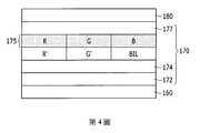
參考第4圖,修改參考第2圖所述的有機發光二極體LD之發射層175。例如,在本例示性實施例中,發射層175可包括紅光發射層R、綠光發射層G、以及藍光發射層B,且可將用於改善藍光發射層B之效率的輔助層BIL配置於藍光發射層B下。Referring to FIG. 4, the
紅光發射層R可為約30奈米至約50奈米厚,綠光發射層G可為約10奈米至約30奈米厚,而藍光發射層B可為約10奈米至約30奈米厚。藍光發射層B下的輔助層BIL可為約20奈米厚或20奈米以下厚。輔助層BIL可調整電洞電荷平衡,且改善藍光發射層B之效率。輔助層BIL可包括由以下化學式1表示的化合物。
在化學式1中,A1、A2、與A3各可為氫、烷基、芳基、咔唑、二苯并噻吩、二苯并呋喃(DBF)、及聯苯,且a、b、與c各可為0至4之間的正數。In chemical formula 1, A1, A2, and A3 can each be hydrogen, alkyl, aryl, carbazole, dibenzothiophene, dibenzofuran (DBF), and biphenyl, and a, b, and c can each be Can be a positive number between 0 and 4.
由化學式1表示的化合物之實例可包括以下化學式1-1、1-2、1-3、1-4、1-5、及1-6。


另一例示性實施例為輔助層BIL可包括由以下化學式2表示的化合物。
在化學式2中,a為0至3,b與c各為0至3,X可選自O、N、與S,且X可各為相同或不同。In Chemical Formula 2, a is 0 to 3, b and c are each 0 to 3, X can be selected from O, N, and S, and X can be the same or different.
由化學式2表示的化合物之示例可包括以下化學式2-1至2-6。


另一例示性實施例為,輔助層BIL可包括由以下化學式3表示的化合物。
在化學式3中,A1可為烷基、芳基、咔唑、二苯并噻吩、及二苯并呋喃(DBF),L1與L2可為
以下將揭述根據一例示性實施例的輔助層BIL之合成方法。例如揭述以下化學式1-1之合成方法。
在氬大氣下,將6.3克之4-二苯并呋喃硼酸(4-dibenzofuran boronic acid)、4.8克之4,4’,4”-三溴三苯基胺(4, 4', 4''-tribromotriphenylamine)、104毫克(mg)之四(三苯基膦)鈀(tetrakis(triphenylphosphine) palladium)(Pd(PPh3)4)、48毫升之碳酸鈉(Na2CO3)溶液(2M)、以及48毫升之甲苯置於300毫升之三頸燒瓶中,且將其在80℃反應8小時。將反應溶液以甲苯/水萃取,且將萃取液以無水硫酸鎂(sodium sulfate)乾燥。將其在低壓下濃縮,及將獲得的粗產物經由管柱純化法精製,藉此得到3.9克之泛白黃色粉末。In an argon atmosphere, 6.3 grams of 4-dibenzofuran boronic acid (4-dibenzofuran boronic acid), 4.8 grams of 4,4',4"-tribromotriphenylamine (4, 4', 4''-tribromotriphenylamine ), 104 milligrams (mg) of tetrakis(triphenylphosphine) palladium (Pd(PPh3 )4 ), 48 ml of sodium carbonate (Na2 CO3 ) solution (2M), and 48 One milliliter of toluene was placed in a 300-ml three-necked flask and reacted at 80°C for 8 hours. The reaction solution was extracted with toluene/water, and the extract was dried with anhydrous magnesium sulfate (sodium sulfate). It was kept at low pressure After concentrating, and purifying the obtained crude product through a column purification method, 3.9 g of whiteish yellow powder is obtained.
參考第4圖,紅光共振輔助層R’可被配置於紅光發射層R下,及綠光共振輔助層G’可被配置於綠光發射層G下。紅光共振輔助層R’及綠光共振輔助層G’為針對各顏色(例如紅或綠色)設定振諧(resonant)距離(共振(resonance)距離)之層。在一些實施例中,未包含藍光共振輔助層。例如可不形成配置於電洞傳輸層174與藍光發射層B及輔助層BIL之間之獨立共振輔助層於對應紅光發射層R或綠光發射層G之藍光發射層B及輔助層BIL下。在一些實施例中,輔助層BIL係物理性接觸電洞傳輸層174。Referring to FIG. 4, the red light resonance auxiliary layer R'may be arranged under the red light emission layer R, and the green light resonance auxiliary layer G'may be arranged under the green light emission layer G. The red light resonance auxiliary layer R'and the green light resonance auxiliary layer G'are layers for setting a resonance distance (resonance distance) for each color (for example, red or green). In some embodiments, the blue resonance auxiliary layer is not included. For example, the independent resonance auxiliary layer disposed between the
雖然在第4圖中未描述,如同相對於第3圖所述的例示性實施例,電子注入層179可在第二電極180與電子傳輸層177之間形成。Although not described in FIG. 4, as in the exemplary embodiment described with respect to FIG. 3, the
除了上述差異以外,相對於第2圖所述者可應用於第4圖之例示性實施例。In addition to the above differences, what is described with respect to FIG. 2 can be applied to the exemplary embodiment of FIG. 4.
第5圖繪示第2圖之有機發光二極體之經修改例示性實施例的橫切面圖。FIG. 5 shows a cross-sectional view of a modified exemplary embodiment of the organic light emitting diode of FIG. 2. FIG.
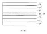
參考第5圖,根據例示性實施例之有機發光二極體可包括第一電極260、發光二極體層270、及第二電極280。配置於第一電極260上的電洞注入層272可包括具功函數為4.3電子伏特或4.3電子伏特以上(高功函數)的金屬。使用具有高功函數的金屬可針對第一電極260與電洞傳輸層274減少電洞注入屏障。電洞注入層272可進一步包含具有不同極性的第一成分及第二成分之偶極性材料及/或具相對介電常數為10或10以上的氧化物。電洞注入層272可藉由將具功函數為4.3電子伏特或4.3電子伏特以上(高功函數)的金屬、第一成分及第二成分之偶極性材料、及具相對介電常數為10或10以上的氧化物之至少之一或至少之二或以上共沉積而形成。Referring to FIG. 5, the organic light emitting diode according to an exemplary embodiment may include a
在本例示性實施例中,當將偶極性材料及/或具相對介電常數為10或10以上的氧化物加入包括具功函數為4.3電子伏特或4.3電子伏特以上(高功函數)的金屬之電洞注入層272時,可在界面上發生平坦化,且穿隧效應可隨電場增加而變得更加容易。例如,在界面上製造的偶極可偏移為有機材料層的電洞傳輸層274或發射層275之真空度(及增加LUMO位階(level)),且可降低注入屏障。In this exemplary embodiment, when a dipolar material and/or an oxide having a relative permittivity of 10 or more is added to include a metal having a work function of 4.3 eV or more (high work function) In the
此外,在根據本例示性實施例之有機發光二極體LD中,包括RbI之電洞注入層272可以非晶薄膜之型式配置於第一電極260上。當第一電極260係由ITO/Ag/ITO製成時,Ag可能傳輸通過結晶ITO至有機材料層,且可能會減損發光性質。In addition, in the organic light emitting diode LD according to this exemplary embodiment, the
電洞注入層272之具功函數為4.3電子伏特或4.3電子伏特以上(高功函數)的金屬可包括Ag、Au、B、Be、C、Co、Cr、Cu、Fe、Hg、Ir、Mo、Nb、Ni、Os、Pd、Pt、Re、Rh、Ru、Sb、Se、Si、Sn、Ta、Te、Ti、V、W、或Zn之一或多個。The metal with a work function of 4.3 electron volts or more (high work function) of the
電洞注入層272中之偶極性材料的第一成分及第二成分之偶極矩可為5德拜或5德拜以上。第一成分可包括週期表中之鹼金屬、鹼土金屬、稀土元素、或過渡金屬之一或多個,且第二成分可包括鹵素。第一成分可包括具功函數為3.0電子伏特或3.0電子伏特以上,且選自Li、Na、K、Rb、Cs、Ca、Sr、Ba、Ce、Sm、Eu、Gd、Yb、或其合金者之一或多個。The dipole moments of the first component and the second component of the dipolar material in the
電洞注入層272中具相對介電常數為10或10以上的氧化物可包括WO3、MoO3、Cu2O、Yb2O3、Sm2O3、Nb2O3、Gd2O3、Eu2O3之一或多個。The oxide with a relative dielectric constant of 10 or more in the
電洞注入層272上的電洞傳輸層274、發射層275、電子傳輸層277、及第二電極280可依循相對於第2圖所述者。The
第6圖繪示將第5圖之有機發光二極體作部分修改之例示性實施例的橫切面圖。FIG. 6 is a cross-sectional view of an exemplary embodiment in which the organic light emitting diode of FIG. 5 is partially modified.
參考第6圖,其描述根據第5圖之例示性實施例的有機發光二極體LD中具有電子注入層279之結構。在本例示性實施例中,電子注入層279可被配置於電子傳輸層277與第二電極280之間。電子注入層279可使電子易於從第二電極280被注入至電子傳輸層277。在本例示性實施例中,電子注入層279可包括具低功函數的金屬。電子注入層279用之金屬之功函數可為3.0電子伏特或3.0電子伏特以下。例如,電子注入層279可由鹼金屬、鹼土金屬、稀土元素、鹼金屬氧化物、鹼土金屬氧化物、稀土氧化物、或其合金之一或多個製成。電子注入層279可包括Li、Na、K、Rb、Cs、Ca、Sr、Ba、Ce、Sm、Eu、Gd、Yb、或其合金之一或多個。Referring to FIG. 6, it describes the structure of the organic light emitting diode LD with the
除了上述差異以外,相對於第5圖所述者可應用於第6圖之例示性實施例。In addition to the above differences, what is described with respect to FIG. 5 can be applied to the exemplary embodiment of FIG. 6.
第7圖繪示將第5圖之有機發光二極體作部分修改之例示性實施例的橫切面圖。FIG. 7 is a cross-sectional view of an exemplary embodiment in which the organic light emitting diode of FIG. 5 is partially modified.
參考第7圖,其描述根據第5圖之例示性實施例的有機發光二極體LD中具有雙層電洞注入層272之結構。在本例示性實施例中,電洞注入層272可包括第一電洞注入層272-1及第二電洞注入層272-2。第一電洞注入層272-1及第二電洞注入層272-2各可藉由將具功函數為4.3電子伏特或4.3電子伏特以上(高功函數)的金屬、第一成分及第二成分之偶極性材料、及具相對介電常數為10或10以上的氧化物之至少之一或至少之二或以上共沉積而形成。第一電洞注入層272-1及第二電洞注入層272-2可由相同材料製成,或者可包括不同的材料。Referring to FIG. 7, it describes the structure of the organic light emitting diode LD according to the exemplary embodiment of FIG. 5 having the double-layer
除了上述差異以外,相對於第5圖所述者可應用於第7圖之例示性實施例。In addition to the above differences, what is described with respect to FIG. 5 can be applied to the exemplary embodiment of FIG. 7.
第8圖描述將第5圖之有機發光二極體作部分修改之例示性實施例的橫切面圖。Fig. 8 depicts a cross-sectional view of an exemplary embodiment in which the organic light emitting diode of Fig. 5 is partially modified.
參考第8圖,其描述根據第5圖之例示性實施例的有機發光二極體LD中具有三層電洞注入層272之結構。在本例示性實施例中,電洞注入層272可包括第一電洞注入層272-1、第二電洞注入層272-2、及第三電洞注入層272-3。第一電洞注入層272-1、第二電洞注入層272-2、及第三電洞注入層272-3各可藉由將具功函數為4.3電子伏特或4.3電子伏特以上(高功函數)的金屬、第一成分及第二成分之偶極性材料、及具相對介電常數為10或10以上的氧化物之至少之一或至少之二或以上共沉積而形成。第一電洞注入層272-1、第二電洞注入層272-2、及第三電洞注入層272-3可由相同的材料製成,或者可包括不同的材料。With reference to FIG. 8, it describes the structure of the organic light emitting diode LD according to the exemplary embodiment of FIG. 5 having three hole injection layers 272. In this exemplary embodiment, the
除了上述差異以外,相對於第5圖所述者可應用於第8圖之例示性實施例。In addition to the above differences, what is described with respect to FIG. 5 can be applied to the exemplary embodiment of FIG. 8.
第9圖繪示將第5圖之有機發光二極體作部分修改之例示性實施例的橫切面圖。FIG. 9 is a cross-sectional view of an exemplary embodiment in which the organic light emitting diode of FIG. 5 is partially modified.
參考第9圖,其修改參考第5圖所述的有機發光二極體LD之發射層275。例如,在本例示性實施例中,發射層275可包括紅光發射層R、綠光發射層G、與藍光發射層B,且可將用於改善藍光發射層B之效率的輔助層BIL配置於藍光發射層B下。Referring to FIG. 9, the
紅光發射層R、綠光發射層G、藍光發射層B、及藍光發射層B下的輔助層BIL之說明可參照相對於第4圖所述者。The description of the red light emitting layer R, the green light emitting layer G, the blue light emitting layer B, and the auxiliary layer BIL under the blue light emitting layer B can refer to those described with respect to FIG. 4.
參考第9圖,紅光共振輔助層R’可被配置於紅光發射層R下,且綠光共振輔助層G’可被配置於綠光發射層G下。紅光共振輔助層R’及綠光共振輔助層G’為針對各顏色(例如紅或綠色)設定振諧距離(共振距離)之層。在一些實施例中,未包含藍光共振輔助層。例如,可不形成配置於電洞傳輸層274與藍光發射層B及輔助層BIL之間的獨立共振輔助層於對應紅光發射層R或綠光發射層G之藍光發射層B及輔助層BIL下。在一些實施例中,輔助層BIL係物理性接觸電洞傳輸層274。Referring to FIG. 9, the red light resonance auxiliary layer R'may be arranged under the red light emitting layer R, and the green light resonance auxiliary layer G'may be arranged under the green light emitting layer G. The red light resonance auxiliary layer R'and the green light resonance auxiliary layer G'are layers in which the resonance distance (resonance distance) is set for each color (for example, red or green). In some embodiments, the blue resonance auxiliary layer is not included. For example, the independent resonance auxiliary layer disposed between the
雖然在第9圖中未描述,但如同相對於第6圖所述的例示性實施例,電子注入層279可在第二電極280與電子傳輸層277之間形成。Although not described in FIG. 9, as in the exemplary embodiment described with respect to FIG. 6, the
除了上述差異以外,相對於第5圖所述者可應用於第9圖之例示性實施例。In addition to the above differences, what is described with respect to FIG. 5 can be applied to the exemplary embodiment of FIG. 9.
藉由總結及回顧,為自發光型之有機發光顯示裝置可具有大視角、優良對比度、及快速回應性。有機發光顯示裝置可包括有機發光二極體,從一電極注入的電子與從另一電極注入的電洞可在發射層結合而可產生激子,該激子可發射能量而可發光。By summarizing and reviewing, the self-luminous organic light emitting display device can have a large viewing angle, excellent contrast, and fast response. The organic light emitting display device may include an organic light emitting diode, and electrons injected from one electrode and holes injected from the other electrode can be combined in the emission layer to generate excitons, which can emit energy and emit light.
本發明提供一種可具有高效率及長使用壽命之有機發光二極體、及一種包含該有機發光二極體之有機發光顯示裝置。根據一例示性實施例,可形成包含偶極性材料之電洞注入層,且可增加發射效率。根據一例示性實施例,其可在藍光發射層下形成輔助層,且可增加藍光發射層之發射效率。The present invention provides an organic light-emitting diode with high efficiency and long service life, and an organic light-emitting display device including the organic light-emitting diode. According to an exemplary embodiment, a hole injection layer including a dipolar material can be formed, and emission efficiency can be increased. According to an exemplary embodiment, an auxiliary layer can be formed under the blue light emitting layer, and the emission efficiency of the blue light emitting layer can be increased.
現已在此揭示例示性實施例,且雖然使用指定術語,但其僅以一般性及說明性方式使用及解讀,而非用於限制目的。如對本申請案所屬技術領域中具有通常知識者而言為顯而易知的,在一些情況中,除非另有特定地指示,否則搭配特定實施例所述之特點、特徵、及/或要素可單獨或結合搭配其他實施例所述之特點、特徵、及/或要素而使用。因此,所屬技術領域中具有通常知識者將了解的是,可進行各種形式及細節之變化而不背離由以下申請專利範圍所述的本發明之精神及範圍。Exemplary embodiments are now disclosed here, and although designated terms are used, they are only used and interpreted in a general and illustrative manner, not for limiting purposes. If it is obvious to those with ordinary knowledge in the technical field to which this application belongs, in some cases, unless specifically indicated otherwise, the features, features, and/or elements described in the specific embodiments may be combined. Used alone or in combination with the features, features, and/or elements described in other embodiments. Therefore, those with ordinary knowledge in the technical field will understand that various forms and details can be changed without departing from the spirit and scope of the present invention described in the scope of the following patent applications.
121‧‧‧薄膜封裝層121a、121c‧‧‧有機密封層121b、121d‧‧‧無機密封層122a‧‧‧第一接觸孔122b‧‧‧第二接觸孔122c‧‧‧第三接觸孔123‧‧‧基板124‧‧‧平坦化層125‧‧‧像素定義層126‧‧‧基板緩衝層127‧‧‧閘極絕緣層128‧‧‧層間絕緣層130‧‧‧薄膜電晶體131‧‧‧驅動源極電極132‧‧‧驅動汲極電極133‧‧‧驅動閘極電極134‧‧‧源極區域135‧‧‧通道區域136‧‧‧汲極區域137‧‧‧驅動半導體層160、260‧‧‧第一電極170、270‧‧‧發光二極體層172、272‧‧‧電洞注入層174、274‧‧‧電洞傳輸層175、275‧‧‧發射層177、277‧‧‧電子傳輸層179、279‧‧‧電子注入層180、280‧‧‧第二電極190‧‧‧外塗層272-1‧‧‧第一電洞注入層272-2‧‧‧第二電洞注入層272-3‧‧‧第三電洞注入層B‧‧‧藍光發射層BIL‧‧‧輔助層LD‧‧‧有機發光二極體X‧‧‧部分R‧‧‧紅光發射層R’‧‧‧紅光共振輔助層G‧‧‧綠光發射層G’‧‧‧綠光共振輔助層121‧‧‧Thin Film Encapsulation Layer121a, 121c‧‧‧organic sealing layer121b, 121d‧‧‧Inorganic sealing layer122a‧‧‧First contact hole122b‧‧‧Second contact hole122c‧‧‧Third contact hole123‧‧‧Substrate124‧‧‧Planarization layer125‧‧‧Pixel Definition Layer126‧‧‧Substrate buffer layer127‧‧‧Gate insulation layer128‧‧‧Interlayer insulation130‧‧‧Thin Film Transistor131‧‧‧Drive source electrode132‧‧‧Drain electrode133‧‧‧Drive gate electrode134‧‧‧Source area135‧‧‧Access area136‧‧‧Dip pole area137‧‧‧Drive semiconductor layer160、260‧‧‧First electrode170、270‧‧‧Light-emitting diode layer172, 272‧‧‧hole injection layer174、274‧‧‧hole transmission layer175、275‧‧‧Launching layer177, 277‧‧‧ electron transport layer179、279‧‧‧Electron injection layer180、280‧‧‧Second electrode190‧‧‧Outer coating272-1‧‧‧The first hole injection layer272-2‧‧‧Second hole injection layer272-3‧‧‧The third hole injection layerB‧‧‧Blue light emitting layerBIL‧‧‧Auxiliary layerLD‧‧‧Organic Light Emitting DiodeX‧‧‧PartR‧‧‧Red light emitting layerR’‧‧‧Red light resonance auxiliary layerG‧‧‧Green light emitting layerG’‧‧‧Green light resonance auxiliary layer
對於所屬技術領域中具有通常知識者而言本發明之特點藉由參考附圖來詳細說明例示性實施例將變得顯而易知,其中:For those with ordinary knowledge in the art, the characteristics of the present invention will become apparent by referring to the drawings to describe the exemplary embodiments in detail, in which:
第1圖繪示根據一例示性實施例之有機發光顯示裝置的橫切面圖;FIG. 1 is a cross-sectional view of an organic light emitting display device according to an exemplary embodiment;
第2圖繪示將第1圖之有機發光二極體放大之橫切面圖;Figure 2 shows an enlarged cross-sectional view of the organic light emitting diode of Figure 1;
第3圖繪示將第2圖之有機發光二極體作部分修改之例示性實施例的橫切面圖;Figure 3 shows a cross-sectional view of an exemplary embodiment in which the organic light emitting diode of Figure 2 is partially modified;
第4圖繪示將第2圖之有機發光二極體作部分修改之例示性實施例的橫切面圖;Figure 4 shows a cross-sectional view of an exemplary embodiment in which the organic light emitting diode of Figure 2 is partially modified;
第5圖繪示第2圖之有機發光二極體之經修改例示性實施例的橫切面圖;Figure 5 shows a cross-sectional view of a modified exemplary embodiment of the organic light emitting diode of Figure 2;
第6圖繪示將第5圖之有機發光二極體作部分修改之例示性實施例的橫切面圖;Fig. 6 shows a cross-sectional view of an exemplary embodiment in which the organic light emitting diode of Fig. 5 is partially modified;
第7圖繪示將第5圖之有機發光二極體作部分修改之例示性實施例的橫切面圖;FIG. 7 shows a cross-sectional view of an exemplary embodiment in which the organic light emitting diode of FIG. 5 is partially modified;
第8圖繪示將第5圖之有機發光二極體作部分修改之例示性實施例的橫切面圖;及Fig. 8 shows a cross-sectional view of an exemplary embodiment in which the organic light emitting diode of Fig. 5 is partially modified; and
第9圖繪示將第5圖之有機發光二極體作部分修改之例示性實施例的橫切面圖。FIG. 9 is a cross-sectional view of an exemplary embodiment in which the organic light emitting diode of FIG. 5 is partially modified.
121‧‧‧薄膜封裝層121‧‧‧Thin Film Encapsulation Layer
121a、121c‧‧‧有機密封層121a, 121c‧‧‧organic sealing layer
121b、121d‧‧‧無機密封層121b, 121d‧‧‧Inorganic sealing layer
122a‧‧‧第一接觸孔122a‧‧‧First contact hole
122b‧‧‧第二接觸孔122b‧‧‧Second contact hole
122c‧‧‧第三接觸孔122c‧‧‧Third contact hole
123‧‧‧基板123‧‧‧Substrate
124‧‧‧平坦化層124‧‧‧Planarization layer
125‧‧‧像素定義層125‧‧‧Pixel Definition Layer
126‧‧‧基板緩衝層126‧‧‧Substrate buffer layer
127‧‧‧閘極絕緣層127‧‧‧Gate insulation layer
128‧‧‧層間絕緣層128‧‧‧Interlayer insulation
130‧‧‧薄膜電晶體130‧‧‧Thin Film Transistor
131‧‧‧驅動源極電極131‧‧‧Drive source electrode
132‧‧‧驅動汲極電極132‧‧‧Drain electrode
133‧‧‧驅動閘極電極133‧‧‧Drive gate electrode
134‧‧‧源極區域134‧‧‧Source area
135‧‧‧通道區域135‧‧‧Access area
136‧‧‧汲極區域136‧‧‧Dip pole area
137‧‧‧驅動半導體層137‧‧‧Drive semiconductor layer
160‧‧‧第一電極160‧‧‧First electrode
170‧‧‧發光二極體層170‧‧‧Light Emitting Diode Layer
180‧‧‧第二電極180‧‧‧Second electrode
190‧‧‧外塗層190‧‧‧Outer coating
LD‧‧‧有機發光二極體LD‧‧‧Organic Light Emitting Diode
X‧‧‧部分X‧‧‧Part
Claims (13)
Translated fromChinese
Applications Claiming Priority (2)
| Application Number | Priority Date | Filing Date | Title |
|---|---|---|---|
| KR10-2014-0109198 | 2014-08-21 | ||
| KR1020140109198AKR101733151B1 (en) | 2014-08-21 | 2014-08-21 | Organic light emitting diode and organic light emitting display device including the same |
Publications (2)
| Publication Number | Publication Date |
|---|---|
| TW201614892A TW201614892A (en) | 2016-04-16 |
| TWI703751Btrue TWI703751B (en) | 2020-09-01 |
Family
ID=55349028
Family Applications (1)
| Application Number | Title | Priority Date | Filing Date |
|---|---|---|---|
| TW104127236ATWI703751B (en) | 2014-08-21 | 2015-08-20 | Organic light emitting display device including organic light emitting diode |
Country Status (4)
| Country | Link |
|---|---|
| US (1) | US10367163B2 (en) |
| KR (1) | KR101733151B1 (en) |
| CN (1) | CN105390522B (en) |
| TW (1) | TWI703751B (en) |
Families Citing this family (20)
| Publication number | Priority date | Publication date | Assignee | Title |
|---|---|---|---|---|
| KR101733151B1 (en)* | 2014-08-21 | 2017-05-08 | 삼성디스플레이 주식회사 | Organic light emitting diode and organic light emitting display device including the same |
| KR102343655B1 (en)* | 2014-12-24 | 2021-12-27 | 삼성디스플레이 주식회사 | Organic light emitting diode and organic light emitting display device including the same |
| US20170294628A1 (en)* | 2016-04-07 | 2017-10-12 | Samsung Display Co., Ltd. | Organic Light Emitting Diode and Light Emitting Diode Display |
| KR102543575B1 (en) | 2016-04-07 | 2023-06-14 | 삼성디스플레이 주식회사 | Organic light emitting diode |
| CN109196680B (en) | 2016-05-10 | 2020-10-27 | 株式会社Lg化学 | Organic electroluminescent device and method of making the same |
| KR102522667B1 (en)* | 2016-06-13 | 2023-04-17 | 삼성디스플레이 주식회사 | Display device |
| KR102642330B1 (en) | 2016-07-19 | 2024-03-05 | 삼성디스플레이 주식회사 | Organic light emitting diode and display device including the same |
| KR102708001B1 (en) | 2017-02-15 | 2024-09-20 | 삼성디스플레이 주식회사 | Light emitting diode and display device including the same |
| KR102362185B1 (en)* | 2017-06-21 | 2022-02-11 | 삼성디스플레이 주식회사 | Light emitting diode and display device including the same |
| EP3747876B1 (en)* | 2018-01-29 | 2023-03-08 | Idemitsu Kosan Co.,Ltd. | Compound and organic electroluminescent element using same |
| KR20200072647A (en)* | 2018-12-12 | 2020-06-23 | 삼성디스플레이 주식회사 | Organic electroluminescence device and display device including the same |
| KR102169567B1 (en) | 2018-12-21 | 2020-10-23 | 엘지디스플레이 주식회사 | Organic Light Emitting Device |
| KR102169568B1 (en) | 2018-12-21 | 2020-10-23 | 엘지디스플레이 주식회사 | Organic Light Emitting Device |
| KR20210090331A (en)* | 2020-01-09 | 2021-07-20 | 삼성디스플레이 주식회사 | Organic light emitting device |
| CN113540368A (en)* | 2020-04-20 | 2021-10-22 | Tcl科技集团股份有限公司 | Composite material, preparation method thereof and quantum dot light-emitting diode |
| KR102820733B1 (en) | 2020-08-21 | 2025-06-16 | 삼성디스플레이 주식회사 | Organic light-emitting diode and manufacturing the same |
| CN114512617A (en)* | 2020-11-17 | 2022-05-17 | 京东方科技集团股份有限公司 | Light-emitting device, display device and manufacturing method of light-emitting device |
| US12396075B2 (en) | 2020-12-17 | 2025-08-19 | Boe Technology Group Co., Ltd. | Blue organic electroluminescence device, display panel and display apparatus |
| CN112635691B (en)* | 2020-12-31 | 2022-07-12 | Tcl华星光电技术有限公司 | Array substrate and manufacturing method thereof |
| KR20220102708A (en) | 2021-01-13 | 2022-07-21 | 삼성디스플레이 주식회사 | Light-emitting device and electronic apparatus including the same |
Citations (6)
| Publication number | Priority date | Publication date | Assignee | Title |
|---|---|---|---|---|
| TW200727739A (en)* | 2006-01-13 | 2007-07-16 | Au Optronics Corp | Organic electro-luminescence device |
| TW200936545A (en)* | 2007-12-21 | 2009-09-01 | Idemitsu Kosan Co | Organic electroluminescent device |
| TW200943600A (en)* | 2007-04-03 | 2009-10-16 | Univ Tsinghua | Organic electroluminescent device |
| TW201004010A (en)* | 2008-04-17 | 2010-01-16 | Fuji Electric Holdings | Organic light emitting diode device |
| TW201248963A (en)* | 2011-03-04 | 2012-12-01 | Sony Corp | Organic EL display device and method of manufacturing the same |
| TW201426994A (en)* | 2012-12-27 | 2014-07-01 | Lg Display Co Ltd | Organic light emitting diode display device and method of manufacturing same |
Family Cites Families (40)
| Publication number | Priority date | Publication date | Assignee | Title |
|---|---|---|---|---|
| JP3295088B2 (en)* | 1993-09-29 | 2002-06-24 | 出光興産株式会社 | Organic electroluminescence device |
| JP3529543B2 (en) | 1995-04-27 | 2004-05-24 | パイオニア株式会社 | Organic electroluminescence device |
| US5677572A (en) | 1996-07-29 | 1997-10-14 | Eastman Kodak Company | Bilayer electrode on a n-type semiconductor |
| KR101200860B1 (en) | 2004-05-28 | 2012-11-13 | 글로벌 오엘이디 테크놀러지 엘엘씨 | Tandem oled having stable intermediate connectors |
| KR101030008B1 (en) | 2004-12-31 | 2011-04-20 | 삼성모바일디스플레이주식회사 | Organic electroluminescent element |
| KR100741104B1 (en) | 2005-12-30 | 2007-07-20 | 삼성에스디아이 주식회사 | Organic light emitting device |
| JP2009044104A (en) | 2007-08-10 | 2009-02-26 | Sumitomo Chemical Co Ltd | Organic electroluminescence device and manufacturing method |
| WO2009085344A2 (en)* | 2007-12-28 | 2009-07-09 | Universal Display Corporation | Dibenzothiophene-containing materials in phosphorescent light emitting diodes |
| KR100922755B1 (en) | 2007-12-28 | 2009-10-21 | 삼성모바일디스플레이주식회사 | Organic light emitting device |
| KR100922759B1 (en) | 2008-02-26 | 2009-10-21 | 삼성모바일디스플레이주식회사 | Organic light emitting device |
| JP5698135B2 (en)* | 2008-09-04 | 2015-04-08 | ユニバーサル ディスプレイ コーポレイション | White phosphorescent organic light emitting device |
| US8778511B2 (en)* | 2008-12-12 | 2014-07-15 | Universal Display Corporation | OLED stability via doped hole transport layer |
| KR101609275B1 (en)* | 2008-12-16 | 2016-04-06 | 삼성디스플레이 주식회사 | Organic Compound and Organic Light Emitting Device Includign the Same |
| WO2011074633A1 (en) | 2009-12-16 | 2011-06-23 | パナソニック電工株式会社 | Organic electroluminescent element |
| KR101647134B1 (en) | 2010-03-29 | 2016-08-10 | 삼성디스플레이 주식회사 | Organic Light Emitting Device |
| JP5653179B2 (en)* | 2010-11-05 | 2015-01-14 | キヤノン株式会社 | Phenanthrene compound and organic light emitting device using the same |
| CN103534833B (en)* | 2011-05-13 | 2016-07-20 | 索尼株式会社 | Organic Electroluminescent Multicolor Light-Emitting Device |
| KR20130022986A (en) | 2011-08-26 | 2013-03-07 | 엘지디스플레이 주식회사 | Organic electro-luminescence display |
| CN103050641B (en) | 2011-10-14 | 2016-03-02 | 乐金显示有限公司 | The display panel of organic luminescent device and this device of use |
| CN104737321B (en)* | 2012-07-31 | 2018-05-11 | 株式会社Lg化学 | Substrate for organic electronic device |
| KR101497138B1 (en)* | 2012-08-21 | 2015-02-27 | 제일모직 주식회사 | Organic optoelectronic device and display including the same |
| KR101975570B1 (en) | 2012-11-06 | 2019-08-26 | 삼성디스플레이 주식회사 | Thin film transistor array panel and organic light emitting diode display including the same |
| KR101684979B1 (en) | 2012-12-31 | 2016-12-09 | 제일모직 주식회사 | Organic optoelectronic device and display including the same |
| KR101998627B1 (en) | 2013-01-25 | 2019-07-11 | 삼성디스플레이 주식회사 | Organic electroluminescent device and manufacturing method thereof |
| US9391124B2 (en)* | 2013-07-02 | 2016-07-12 | Samsung Display Co., Ltd. | Organic light emitting diode display |
| KR102231935B1 (en)* | 2013-08-05 | 2021-03-25 | 덕산네오룩스 주식회사 | Organic electric element comprising compound for organic electric element and electronic device thereof |
| US9853229B2 (en)* | 2013-10-23 | 2017-12-26 | University Of Southern California | Organic electroluminescent materials and devices |
| US9450198B2 (en)* | 2014-04-15 | 2016-09-20 | Universal Display Corporation | Organic electroluminescent materials and devices |
| KR101733151B1 (en)* | 2014-08-21 | 2017-05-08 | 삼성디스플레이 주식회사 | Organic light emitting diode and organic light emitting display device including the same |
| KR101668030B1 (en)* | 2014-08-21 | 2016-10-21 | 삼성디스플레이 주식회사 | Organic light emitting diode and organic light emitting display device including the same |
| US10003041B2 (en)* | 2014-08-21 | 2018-06-19 | Samsung Display Co., Ltd. | Organic light emitting diode and organic light emitting display device including the same |
| US10236464B2 (en)* | 2014-08-21 | 2019-03-19 | Samsung Display Co., Ltd. | Organic light emitting diode |
| KR102343279B1 (en)* | 2014-10-01 | 2021-12-24 | 삼성디스플레이 주식회사 | Organic light emitting diode and organic light emitting display device including the same |
| KR102343655B1 (en)* | 2014-12-24 | 2021-12-27 | 삼성디스플레이 주식회사 | Organic light emitting diode and organic light emitting display device including the same |
| KR102277378B1 (en)* | 2015-01-19 | 2021-07-14 | 삼성디스플레이 주식회사 | Organic light emitting diode and organic light emitting display device including the same |
| KR102459818B1 (en)* | 2015-05-06 | 2022-10-27 | 삼성디스플레이 주식회사 | Organic light emitting diode display |
| KR20160141931A (en)* | 2015-06-01 | 2016-12-12 | 삼성디스플레이 주식회사 | Organic light emitting diode and organic light emitting diode display including the same |
| KR102392044B1 (en)* | 2015-06-15 | 2022-04-28 | 삼성디스플레이 주식회사 | Organic light emitting diode and organic light emitting diode display including the same |
| KR102407115B1 (en)* | 2015-06-25 | 2022-06-09 | 삼성디스플레이 주식회사 | Organic light emitting diode display |
| KR102545675B1 (en)* | 2016-05-11 | 2023-06-20 | 삼성디스플레이 주식회사 | Organic light emitting diode |
- 2014
- 2014-08-21KRKR1020140109198Apatent/KR101733151B1/enactiveActive
- 2015
- 2015-06-11USUS14/736,663patent/US10367163B2/enactiveActive
- 2015-08-18CNCN201510508292.4Apatent/CN105390522B/enactiveActive
- 2015-08-20TWTW104127236Apatent/TWI703751B/enactive
Patent Citations (6)
| Publication number | Priority date | Publication date | Assignee | Title |
|---|---|---|---|---|
| TW200727739A (en)* | 2006-01-13 | 2007-07-16 | Au Optronics Corp | Organic electro-luminescence device |
| TW200943600A (en)* | 2007-04-03 | 2009-10-16 | Univ Tsinghua | Organic electroluminescent device |
| TW200936545A (en)* | 2007-12-21 | 2009-09-01 | Idemitsu Kosan Co | Organic electroluminescent device |
| TW201004010A (en)* | 2008-04-17 | 2010-01-16 | Fuji Electric Holdings | Organic light emitting diode device |
| TW201248963A (en)* | 2011-03-04 | 2012-12-01 | Sony Corp | Organic EL display device and method of manufacturing the same |
| TW201426994A (en)* | 2012-12-27 | 2014-07-01 | Lg Display Co Ltd | Organic light emitting diode display device and method of manufacturing same |
Also Published As
| Publication number | Publication date |
|---|---|
| CN105390522B (en) | 2020-10-30 |
| US10367163B2 (en) | 2019-07-30 |
| KR101733151B1 (en) | 2017-05-08 |
| CN105390522A (en) | 2016-03-09 |
| TW201614892A (en) | 2016-04-16 |
| US20160056387A1 (en) | 2016-02-25 |
| KR20160023992A (en) | 2016-03-04 |
Similar Documents
| Publication | Publication Date | Title |
|---|---|---|
| TWI703751B (en) | Organic light emitting display device including organic light emitting diode | |
| TWI688140B (en) | Organic light emitting diode | |
| US9960380B2 (en) | Organic light emitting diode and organic light emitting display device including the same | |
| TWI693733B (en) | Organic light emitting diode | |
| US20160380235A1 (en) | Organic light emitting diode display | |
| TWI712334B (en) | Organic light emitting element | |
| TWI700845B (en) | Organic light emitting display including organic light emitting element | |
| US9608227B2 (en) | Organic light emitting diode display | |
| KR102392044B1 (en) | Organic light emitting diode and organic light emitting diode display including the same | |
| CN105390618B (en) | organic light emitting diode | |
| KR20160141931A (en) | Organic light emitting diode and organic light emitting diode display including the same |