TWI702810B - Radio frequency device - Google Patents
Radio frequency deviceDownload PDFInfo
- Publication number
- TWI702810B TWI702810BTW106138260ATW106138260ATWI702810BTW I702810 BTWI702810 BTW I702810BTW 106138260 ATW106138260 ATW 106138260ATW 106138260 ATW106138260 ATW 106138260ATW I702810 BTWI702810 BTW I702810B
- Authority
- TW
- Taiwan
- Prior art keywords
- antenna
- conductive trace
- radio frequency
- frequency device
- patent application
- Prior art date
Links
- 238000002955isolationMethods0.000claimsdescription32
- 238000010586diagramMethods0.000description30
- 230000008878couplingEffects0.000description6
- 238000010168coupling processMethods0.000description6
- 238000005859coupling reactionMethods0.000description6
- 238000000465mouldingMethods0.000description6
- 230000005672electromagnetic fieldEffects0.000description5
- 238000005516engineering processMethods0.000description5
- 230000006872improvementEffects0.000description5
- 238000000034methodMethods0.000description4
- 238000004891communicationMethods0.000description3
- 239000004020conductorSubstances0.000description3
- 229910052751metalInorganic materials0.000description3
- 239000002184metalSubstances0.000description3
- 238000004519manufacturing processMethods0.000description2
- 229910000679solderInorganic materials0.000description2
- RYGMFSIKBFXOCR-UHFFFAOYSA-NCopperChemical compound[Cu]RYGMFSIKBFXOCR-UHFFFAOYSA-N0.000description1
- 229910052782aluminiumInorganic materials0.000description1
- XAGFODPZIPBFFR-UHFFFAOYSA-NaluminiumChemical compound[Al]XAGFODPZIPBFFR-UHFFFAOYSA-N0.000description1
- 230000002238attenuated effectEffects0.000description1
- 239000011230binding agentSubstances0.000description1
- 230000005540biological transmissionEffects0.000description1
- 238000006243chemical reactionMethods0.000description1
- 150000001875compoundsChemical class0.000description1
- 229910052802copperInorganic materials0.000description1
- 239000010949copperSubstances0.000description1
- 230000007423decreaseEffects0.000description1
- 230000000694effectsEffects0.000description1
- 238000005530etchingMethods0.000description1
- PCHJSUWPFVWCPO-UHFFFAOYSA-NgoldChemical compound[Au]PCHJSUWPFVWCPO-UHFFFAOYSA-N0.000description1
- 229910052737goldInorganic materials0.000description1
- 239000010931goldSubstances0.000description1
- 238000012986modificationMethods0.000description1
- 230000004048modificationEffects0.000description1
- 238000004806packaging method and processMethods0.000description1
- 230000005855radiationEffects0.000description1
- 229920006395saturated elastomerPolymers0.000description1
- WFKWXMTUELFFGS-UHFFFAOYSA-NtungstenChemical compound[W]WFKWXMTUELFFGS-UHFFFAOYSA-N0.000description1
- 229910052721tungstenInorganic materials0.000description1
- 239000010937tungstenSubstances0.000description1
Images


Classifications
- H—ELECTRICITY
- H04—ELECTRIC COMMUNICATION TECHNIQUE
- H04B—TRANSMISSION
- H04B1/00—Details of transmission systems, not covered by a single one of groups H04B3/00 - H04B13/00; Details of transmission systems not characterised by the medium used for transmission
- H04B1/38—Transceivers, i.e. devices in which transmitter and receiver form a structural unit and in which at least one part is used for functions of transmitting and receiving
- H04B1/40—Circuits
Landscapes
- Engineering & Computer Science (AREA)
- Computer Networks & Wireless Communication (AREA)
- Signal Processing (AREA)
- Variable-Direction Aerials And Aerial Arrays (AREA)
- Details Of Aerials (AREA)
Abstract
Description
Translated fromChinese本發明係有關於通信技術領域,且特別有關於射頻設備。The present invention relates to the field of communication technology, and particularly relates to radio frequency equipment.
從3kHz到300GHz的電磁波頻率有時被稱為射頻(Radio Frequency,RF)。RF信號已被用於許多應用,如通信和雷達。一些射頻設備採用天線。The electromagnetic wave frequency from 3kHz to 300GHz is sometimes referred to as radio frequency (RF). RF signals have been used in many applications, such as communications and radar. Some radio frequency equipment uses antennas.
本發明的實施例提供射頻設備,可減小射頻設備的天線支架的不期望的耦合。The embodiment of the present invention provides a radio frequency device, which can reduce undesired coupling of the antenna support of the radio frequency device.
根據本發明的第一實施例,提供一種射頻設備,其可包括:形成在封裝的再分配層中的第一天線和第二天線;以及形成在所述封裝的所述再分配層中的至少一個導電跡線,所述至少一個導電跡線獨立於所述第一天線和所述第二天線,其中所述第一天線是發射機天線,所述第二天線是接收機天線,並且所述至少一個導電跡線的尺寸和位置被設置成捕獲來自所述第一天線的能量。According to a first embodiment of the present invention, there is provided a radio frequency device, which may include: a first antenna and a second antenna formed in a redistribution layer of a package; and a redistribution layer formed in the package The at least one conductive trace is independent of the first antenna and the second antenna, wherein the first antenna is a transmitter antenna, and the second antenna is a receiver Antenna, and the size and position of the at least one conductive trace are set to capture energy from the first antenna.
根據本發明的第二實施例,提供另一種射頻設備,其可包括:模製層;嵌入模製層內的晶片;耦合到所述晶片的再分配層;形成在所述再分配層中的天線;以及形成在所述再分配層中的導電跡線,所述導電跡線的尺寸和位置被設置以用於捕獲從天線傳輸的能量的一部分。According to a second embodiment of the present invention, there is provided another radio frequency device, which may include: a molding layer; a wafer embedded in the molding layer; a redistribution layer coupled to the wafer; and a redistribution layer formed in the redistribution layer Antenna; and a conductive trace formed in the redistribution layer, the size and position of the conductive trace are set to capture a portion of the energy transmitted from the antenna.
通過以上所述實施例,本發明實施例通過導電跡線捕獲從天線傳輸的能量,由此可減小射頻設備的天線支架的不期望的耦合。Through the above-mentioned embodiments, the embodiment of the present invention captures the energy transmitted from the antenna through the conductive trace, thereby reducing undesired coupling of the antenna support of the radio frequency device.
100:射頻系統100: RF system
104:處理器/控制器104: processor/controller
102:發射機路徑102: Transmitter path
106:發射機前端106: Transmitter front end
108:功率放大器(PA)108: Power Amplifier (PA)
110,310,410,510,610:發射機天線110, 310, 410, 510, 610: transmitter antenna
112:接收機路徑112: receiver path
116:接收機前端116: receiver front end
118:低雜訊放大器(LNA)118: Low Noise Amplifier (LNA)
120,320,520,620:接收機天線120, 320, 520, 620: receiver antenna
200,300,400,500,600:RF設備200, 300, 400, 500, 600: RF equipment
216:平面216: Plane
224,224a,224b,324,424a,424b,524a,524,624a:短截線224, 224a, 224b, 324, 424a, 424b, 524a, 524, 624a: stub
202:晶片202: chip
204:模製層204: Molded layer
206,210,214:電介質層206, 210, 214: Dielectric layer
208,212:再分配層208, 212: Redistribution layer
218:焊球218: Solder Ball
220:金屬層220: Metal layer
222:PCB222: PCB
230,230a,230b:地230, 230a, 230b: ground
228,228b:短截線連接到地的端部228, 228b: the end of the stub connected to the ground
226,226a,226b:短截線的開放端226, 226a, 226b: the open end of the stub
232:天線元件232: antenna element
240:饋線的第三端240: The third end of the feeder
234,334a,334b,434a,434b:饋線234, 334a, 334b, 434a, 434b: feeder
236:饋線的第二端236: The second end of the feeder
241,242,342,442,542,642:曲線241, 242, 342, 442, 542, 642: Curve
244:槽/凹口244: slot/notch
246:槽/凹口的最低點246: lowest point of groove/notch
5C:放大部分5C: Enlarged part
702,704,706:放大部分702, 704, 706: enlarged part
第1圖示出了根據一些實施例的示例性的射頻(RF)系統100的框圖。Figure 1 shows a block diagram of an exemplary radio frequency (RF)
第2A圖示出了根據一些實施例的RF設備200的橫截面圖。Figure 2A shows a cross-sectional view of the
第2B圖示出了根據一些實施例的RF設備200的俯視圖。Figure 2B shows a top view of the
第2C圖示出了根據一些實施例的RF設備200的俯視圖,該俯視圖中展現了電磁場分佈。Figure 2C shows a top view of the
第2D圖是第2A圖-2C的示例性的RF設備200與沒有任何短截線的RF設備的隔離圖的比較圖。Figure 2D is a comparison diagram of the isolation diagrams of the
第3A圖示出根據一些實施例的示例性的RF設備300的俯視圖。Figure 3A shows a top view of an
第3B圖是第3A圖的示例性的RF設備300與沒有任何短截線的RF設備的隔離圖的比較圖。FIG. 3B is a comparison diagram of the isolation diagram of the
第4A圖示出根據一些實施例的示例性的RF設備400的俯視圖。Figure 4A shows a top view of an
第4B圖是第4A圖的示例性的RF設備400與沒有任何短截線的RF設備的隔離圖的比較圖。FIG. 4B is a comparison diagram of the isolation diagram of the
第5A圖示出根據一些實施例的示例性的RF設備500的俯視圖。Figure 5A shows a top view of an
第5B圖是第5A圖的示例性的RF設備500與沒有任何短截線的RF設備的隔離圖的比較圖。FIG. 5B is a comparison diagram of the isolation diagram of the
第5C圖是第5A圖中用橢圓標記出的區域的放大圖。Fig. 5C is an enlarged view of the area marked by an ellipse in Fig. 5A.
第6A圖是示出根據一些實施例的RF設備600的俯視圖。Figure 6A is a top view showing an
第6B圖是RF設備600與沒有任何短截線的RF設備的隔離圖的比較圖。Figure 6B is a comparison diagram of the isolation diagram of the
第7圖示出了根據一些實施例的用於製造本發明所描述的RF設備的示例性方法700。Figure 7 shows an exemplary method 700 for manufacturing the RF device described in the present invention according to some embodiments.
為詳細說明本發明的技術內容、構造特徵、所實現目的及效果,以下結合附圖和實施例對本發明進行詳細說明。In order to explain in detail the technical content, structural features, objectives and effects of the present invention,The present invention will be described in detail below with reference to the drawings and embodiments.
在說明書及後續的申請專利範圍當中使用了某些術語來指稱特定的元件。所屬技術領域技術人員應可理解,硬體製造商可能會用不同的名稱來稱呼同一個元件。本檔並不以名稱的差異來作為區分元件的方式,而是以元件在功能上的差異來作為區分的準則。在接下來的說明書及申請專利範圍中,術語“包含”及“包括”為一開放式的用語,故應解釋成“包含但不限制於”。此外,“耦接”一詞在此包含直接及間接的電性連接手段。因此,如果一個裝置耦接於另一個裝置,則代表該一個裝置可直接電性連接於該另一個裝置,或通過其它裝置或連接手段間接地電性連接至該另一個裝置。In the specification and subsequent patent applications, certain terms are used to refer to specific elements. Those skilled in the art should understand that hardware manufacturers may use different names to refer to the same component. This document does not use differences in names as a way to distinguish components, but uses differences in functions as a criterion. In the following specification and the scope of the patent application, the terms "including" and "including" are open-ended terms, so they should be interpreted as "including but not limited to". In addition, the term "coupled" herein includes direct and indirect electrical connection means. Therefore, if a device is coupled to another device, it means that the one device can be directly and electrically connected to the other device, or indirectly and electrically connected to the other device through other devices or connecting means.
發明人已經認識到並瞭解到,射頻(RF)設備可以包括緊密排列的多個天線。例如,相鄰天線之間的距離可以為0.5mm(毫米)至8mm。在另一示例中,相鄰天線之間的距離可以為0.05 λ至10 λ之內,其中λ是對應於天線的操作頻率的波長。最終,在多個天線之間可能存在電磁耦合,這可能降低RF設備的性能。例如,RF設備中的第一天線可以用於發送信號,並且同一RF設備中的第二天線可以用於接收信號。發射機天線接通時,發射機天線可能會引起電磁場。由於接收機天線位於發射機天線附近,接收機天線可能會捕獲由發射機天線發射的一些功率,這可能會降低接收機天線的性能。例如,接收機天線可能是飽和的並且是衰減的,這將導致惡化的信噪比。發明人還認識到並瞭解到,通過將天線保持在較遠的距離來減小天線之間的電磁耦合會防止RF設備的小型化。The inventors have recognized and understood that radio frequency (RF) devices may include multiple antennas in close array. For example, the distance between adjacent antennas may be 0.5 mm (millimeters) to 8 mm. In another example, the distance between adjacent antennas may be within 0.05 λ to 10 λ, where λ is the wavelength corresponding to the operating frequency of the antenna. Eventually, there may be electromagnetic coupling between multiple antennas, which may degrade the performance of the RF device. For example, the first antenna in the RF device can be used to transmit signals, and the second antenna in the same RF device can be used to receive signals. When the transmitter antenna is switched on, the transmitter antenna may cause electromagnetic fields. Since the receiver antenna is located near the transmitter antenna, the receiver antenna may capture some of the power emitted by the transmitter antenna, which may degrade the performance of the receiver antenna. For example, the receiver antenna may be saturated and attenuated, which will result in a degraded signal-to-noise ratio. The inventor also recognizes and understands that reducing the electromagnetic coupling between the antennas by keeping the antennas at a greater distance prevents the miniaturization of RF devices.
因此,在一些實施例中,提供可以增加RF設備性能而不增加封裝尺寸的技術。最終,當在高頻(例如,在78GHz頻帶)工作時,RF設備可能在天線之間具有高隔離度(例如,小於-30dB的功率傳輸)。在一些實施例中,隔離可以被表示為S21,即從發射機天線傳送到接收機天線的功率。在一些實施例中,S21可以由向量網路分析器測量。在一些實施例中,可以使用已知的發射機天線和已知的接收機天線來測量S21。這些技術中的一種或多種可用於廣泛的應用,包括例如用於汽車的通信和感測設備,移動設備(例如,智慧型電話和平板電腦),雷達和物聯網(Internet of Things,IoT)。Therefore, in some embodiments, a technology that can increase the performance of the RF device without increasing the package size is provided. Finally, when operating at high frequencies (e.g., in the 78 GHz band), the RF device may have high isolation between antennas (e.g., less than -30dB power transmission). In some embodiments, isolation can be expressed as S21, the power transferred from the transmitter antenna to the receiver antenna. In some embodimentsIn, S21 can be measured by vector network analyzer. In some embodiments, a known transmitter antenna and a known receiver antenna may be used to measure S21. One or more of these technologies can be used in a wide range of applications, including, for example, communication and sensing devices for automobiles, mobile devices (for example, smart phones and tablet computers), radar, and the Internet of Things (IoT).
本發明人已經認識到並且意識到一個或多個導電跡線可以被包括在RF設備中,並且導電跡線的尺寸和位置可以被設置以用作能量阱(energy trap),使得從第一天線傳輸的能量的一部分可能被捕獲從而減少第二天線與第一天線之間的不期望的耦合。本發明人進一步認識到並且意識到,一個或多個導電跡線的尺寸和位置可以被設置,使得在保持第一天線和第二天線的性能參數(例如,天線增益,反射係數,輻射圖和效率)的同時抑制第二天線和第一天線之間的不期望的耦合。The inventors have recognized and realized that one or more conductive traces can be included in the RF device, and the size and position of the conductive traces can be set to serve as an energy trap, so that from the first day A portion of the energy transmitted by the wire may be captured to reduce undesired coupling between the second antenna and the first antenna. The present inventors have further realized and realized that the size and position of one or more conductive traces can be set so as to maintain the performance parameters of the first antenna and the second antenna (for example, antenna gain, reflection coefficient, radiation Figure and efficiency) while suppressing undesired coupling between the second antenna and the first antenna.
在一些實施例中,RF設備可以包括形成在再分配層(redistribution layer,RDL)內的多個導電跡線。一個或多個導電跡線可以被配置為一個或多個天線。一個或多個其它導電跡線可被配置為從天線捕獲能量。配置成從天線捕獲能量的導電跡線在本文中可以被稱為短截線(stub)。In some embodiments, the RF device may include a plurality of conductive traces formed in a redistribution layer (RDL). One or more conductive traces can be configured as one or more antennas. One or more other conductive traces may be configured to capture energy from the antenna. Conductive traces configured to capture energy from the antenna may be referred to herein as stubs.
在一些實施例中,短截線可以具有開放端(open end)和連接到參考電位的另一端,所述參考電位可以是地面,直流電壓或另一合適的參考電位。在一些實施例中,每個天線可以具有相關聯的接地環,並且可以存在與天線共用相關聯的接地環的至少一個短截線。在一些實施例中,多個短截線可以與天線共用相同的接地環。In some embodiments, the stub may have an open end and another end connected to a reference potential. The reference potential may be ground, a direct current voltage, or another suitable reference potential. In some embodiments, each antenna may have an associated ground ring, and there may be at least one stub that shares the associated ground ring with the antenna. In some embodiments, multiple stubs may share the same ground ring with the antenna.
在一些實施例中,一個或多個短截線可以放置在RF設備中的一對發射機和接收機天線的外部(假設位於發射機和接收機天線之間)。作為選擇,或額外的部分,可以在發射機和接收機天線之間放置一個或多個短截線。In some embodiments, one or more stubs may be placed outside a pair of transmitter and receiver antennas in the RF device (assuming to be located between the transmitter and receiver antennas). Alternatively, or in addition, one or more stubs can be placed between the transmitter and receiver antennas.
在一些實施例中,一個或多個短截線可以平行於RF設備中的發射機或接收機天線的饋線放置。或者,可以在RF設備中垂直於發射機或接收機天線的饋線放置一個或多個短截線。作為選擇,或額外的部分,一個或多個短截線可以相對於RF設備中的發射機或接收機天線的饋線以一定角度放置。In some embodiments, one or more stubs can be parallel to the transmitter in the RF deviceOr the feeder placement of the receiver antenna. Alternatively, one or more stubs can be placed in the RF equipment perpendicular to the feeder of the transmitter or receiver antenna. Alternatively, or in addition, one or more stubs may be placed at an angle relative to the feeder of the transmitter or receiver antenna in the RF device.
在一些實施例中,RF設備中的發射機和接收機天線中的一個可以具有至少一個相關聯的短截線,而RF設備中的發射機和接收機天線中的另一個天線可能沒有任何相關聯的短截線。In some embodiments, one of the transmitter and receiver antennas in the RF device may have at least one associated stub, while the other antenna in the transmitter and receiver antennas in the RF device may not have any correlation. The stub of the union.
第1圖示出了根據一些實施例的示例性的射頻(RF)系統100的框圖。RF系統100可以包括發射機路徑102和接收機路徑112。在發射機路徑中,處理器/控制器104可以生成載波信號,載波信號可以通過發射機前端106被傳送到功率放大器(PA)108,載波信號可以由PA放大並耦合到發射機天線110。發射機前端可以包括諸如一個或多個濾波器和/或混頻器之類的電路。在接收機路徑中,接收機天線120可以捕獲可由低雜訊放大器(LNA)118放大的信號。放大的信號可以通過接收機前端116發送到處理器/控制器104。接收機前端可以包括諸如一個或多個濾波器和/或混頻器(例如,下變頻混頻器)的電路。Figure 1 shows a block diagram of an exemplary radio frequency (RF)
在一些實施例中,RF系統100可以包括示例性的RF設備200。第2A圖示出了根據一些實施例的RF設備200的橫截面圖。RF設備200可以包括由模製層204封裝的晶片202,第一和第二再分配層(RDL)208和212以及第一,第二和第三電介質層206,210和214,所述第一,第二和第三電介質層206,210和214用於將所述晶片202和所述第一和第二再分配層208和212隔離。第一和第二RDL 208和212可以沿著z方向基本對齊。晶片202的表面和模製層204的表面可以位於相同的平面216上。平面216可以平行於與z方向垂直的x-y平面。第一和第二RDL 208和212可以由鋁,銅,鎢,金或任何其它合適的導電材料或任何數量的導電材料以任何合適的組合形成。在一些實施例中,第一和第二RDL 208和212可以由相同的或者不同的導電材料形成。可形成第一RDL 208以提供訪問晶片202的電通路。可形成第二RDL 212,定義焊球218的焊盤。晶片202可以通過焊球與PCB 222上的金屬層220互連。雖然在該示例中示出了兩個RDL,但是應當理解,本發明並不限於此。RF設備200可以包括一個,三個或任何合適數量的RDL。In some embodiments, the
在一些實施例中,晶片202可以是積體電路晶片。例如,在一些實施例中,晶片202可以是用於微波工程過程的單片微波積體電路(MMIC)晶片。在一些實施例中,晶片202可以包括任何數量的電路或者相關電路的組合,如第1圖所述,所述電路包括例如示例性的發射機前端(TX前端)106,示例性的功率放大器(PA)108,示例性的接收機前端(RX前端)116,示例性的LNA118和/或示例性的處理器/控制器104。In some embodiments, the
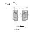
如第2A圖所示,在一些實施例中,發射機天線110和接收機天線120可以形成在第一RDL 208中。發射機天線110可以沿著與z方向垂直的y方向與接收機天線120間隔開。短截線224也可以形成在第一RDL 208中。如第2B圖所示,每個短截線可以具有開放端226(226b)和連接到地230(230b)的端部228(228b)。每個天線可以包括天線元件232和連接到天線元件的饋線234。饋線234可以具有連接到接地230的第一端238,通過例如通孔連接到晶片202的輸出端的第二端236以及連接到天線元件232的第三端240。As shown in FIG. 2A, in some embodiments, the
根據預期的應用,可以使用具有波長λ的無線電波調諧天線。例如,在防碰撞應用(例如,汽車停車助理,自動車輛,家用機器人等)中,用於中距離雷達(例如,10-40米)的RF設備可以在24GHz頻帶上操作,而用於長距離雷達(例如,100-150米)的射頻設備可以被調諧到78GHz頻帶。本發明人已經認識到並且意識到,為了使短截線有效地作為能量阱起作用,可能需要對短截線進行尺寸設定,使得開放端和連接到地面的端部之間的長度基本上等於λ/4的奇數倍,例如λ/4,3 λ/4,5 λ/4等。尺寸的具體設定,可以基於短截線特性,例如當短截線一端保持開路,另一端短截線到地,則工作長度大約是λ/4的奇數倍。然而,本發明並不限於此。短截線可能有任何合適的長度。Depending on the intended application, a radio wave with a wavelength λ can be used to tune the antenna. For example, in anti-collision applications (e.g., car parking assistants, automated vehicles, household robots, etc.), RF equipment used for mid-range radars (e.g., 10-40 meters) can operate in the 24 GHz frequency band and used for long distances Radar (for example, 100-150 meters) radio frequency equipment can be tuned to the 78 GHz band. The inventors have recognized and realized that in order for the stub to function effectively as an energy sink, it may be necessary to size the stub so that the length between the open end and the end connected to the ground is substantially equal to Odd multiples of λ/4, such as λ/4, 3 λ/4, 5 λ/4, etc. The specific size setting can be based on the stub characteristics,For example, when one end of the stub remains open and the other end of the stub is grounded, the working length is approximately an odd multiple of λ/4. However, the present invention is not limited to this. The stub may have any suitable length.
在第2B圖所示的例子中,發射機天線110具有短截線224a(導電跡線),其與發射機天線110共用接地端230a。接地端230a可以基本上圍繞發射機天線。同樣,在第2B圖所示的例子中,接收機天線120具有與接收機天線120共用接地端230b的短截線224b(導電跡線)。接地端230b可以基本上圍繞接收機天線120。在上述示例性的實施例中,接地端230a和230b分別基本上包圍發射機天線和接收機天線。然而,本發明並不限於此。接地端可以具有任何合適的形狀和長度。短截線224a的開放端226a可以指向短截線224b的開放端226b。短截線224a和224b之間的距離可以大於發射機天線和接收機天線之間的距離。在一些實施例中,發射機天線110可以在y方向上與接收機天線120間隔開。短截線224a和224b可以沿y方向伸長。In the example shown in FIG. 2B, the
儘管第2A圖-2B所示的示例性天線具有I形狀類型,應當理解,本發明並不限於此。天線可以是任何合適的類型,包括例如偶極子,資料夾偶極子,環形,矩形環和貼片。儘管在第2A圖-2B所示的實施例中,每個天線具有一個相關聯的短截線,應當理解,本發明不限於此。一個天線可以在不同位置具有多個相關聯的短截線。在一些實施例中,多個短截線可以具有相同的長度或者可以具有不同的長度。儘管示出了兩個天線110和120,但是應當理解,本發明不限於此。一個RF設備可以包括任何合適數量的天線,例如一個,三個,四個或更多個天線。雖然所示的天線可以是發射機天線110和接收機天線120,但是應當理解,本發明不限於此。一個RF設備可以僅包括一個或多個發射機天線,或者僅包括一個或多個接收機天線,或任何合適數量的發射機天線和任何合適數量的接收機天線組合。儘管在這些示例中,短截線具有矩形形狀,但是應當理解,本發明不限於此。各種短截線可以具有任何合適的形狀,包括例如橢圓形,多邊形和/或三角形。Although the exemplary antenna shown in FIGS. 2A to 2B has an I-shape type, it should be understood that the present invention is not limited to this. The antenna can be of any suitable type, including, for example, dipoles, binder dipoles, loops, rectangular loops, and patches. Although in the embodiment shown in FIGS. 2A and 2B, each antenna has an associated stub, it should be understood that the present invention is not limited to this. An antenna can have multiple associated stubs at different locations. In some embodiments, the multiple stubs may have the same length or may have different lengths. Although two
在一些實施例中,當發射機天線110接通(turn on)時,發射機天線可以引起如第2C圖所示的電磁場分佈。電磁場的強度可以與發射的無線電波的強度成比例。可以在短截線224a和224b的開放端增加電磁場的強度,用於表明導電跡線吸引由發射機天線110輻射的能量的一部分。結果,由接收機天線120耦合的能量被減少。In some embodiments, when the
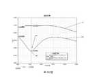
第2D圖是第2A圖-2C的示例性的RF設備200與沒有任何短截線的RF設備的隔離圖的比較圖。隔離圖中的參數S21表示從發射機天線110傳送到接收機天線120的功率。曲線241示出了沒有任何短截線的RF設備的隔離性能。曲線242示出了RF設備200的隔離性能。當曲線241在-30dB以上,而曲線242在所示的頻率範圍內低於-30dB,這表明天線之間的隔離改善。在相同的封裝尺寸下,相較於沒有任何短截線的RF設備,RF設備200可以提供平均10dB的改善。儘管所示出的示例示出了曲線242在78GHz時具有槽/凹口244,但是應當理解,本發明不限於此。本發明人已經認識到並且意識到導電跡線可以根據預期應用來定尺寸和定位。例如,可以包括具有不同長度的多個短截線以在不同頻帶(例如,24GHz處的第一槽/凹口和78GHz的第二槽/凹口)處產生槽/凹口。Figure 2D is a comparison diagram of the isolation diagrams of the
在一些實施例中,槽/凹口的深度可以在1dB至200dB的範圍內。在一些實施例中,槽/凹口的深度可以在2dB至100dB的範圍內。在一些實施例中,槽/凹口的深度可以在5dB至20dB的範圍內。例如,在第2D圖所示的例子中,槽/凹口244具有約9.5dB的深度。In some embodiments, the depth of the groove/notch may be in the range of 1 dB to 200 dB. In some embodiments, the depth of the groove/notch may be in the range of 2dB to 100dB. In some embodiments, the depth of the groove/notch may be in the range of 5dB to 20dB. For example, in the example shown in Figure 2D, the groove/
在一些實施例中,在1dB至200dB的範圍內,槽/凹口的最低點可以小於-30dB。在一些實施例中,在2dB至100dB的範圍內,槽/凹口的最低點可以小於-30dB。在一些實施例中,在5dB至20dB的範圍內,槽/凹口的最低點可以小於-30dB。例如,在第2D圖所示的例子中,槽/凹口244的最低點246約比-30dB低11.9dB。In some embodiments, in the range of 1 dB to 200 dB, the lowest point of the groove/notch may be less than -30 dB. In some embodiments, in the range of 2dB to 100dB, the lowest point of the groove/notch may be less than -30dB. In some embodiments, in the range of 5dB to 20dB, the lowest point of the groove/notch may be less than -30dB. For example, in the example shown in Figure 2D, the
第3A圖示出根據一些實施例的示例性的RF設備300的俯視圖,RF設備300包括放置在可選位置處的短截線。在一些實施例中,RF設備300可以具有與第2A圖-2B所示的示例性的RF設備200相同的封裝尺寸。RF設備300與RF設備200的不同之處在於,短截線324a與第2B圖中示例性的短截線224a在與y方向和z方向垂直的x方向上處於不同的位置,短截線324b與第2B圖中示例性的短截線224b在與y方向和z方向垂直的x方向上處於不同的位置,此外,第3A圖中天線310還包括饋線334a,天線320還包括饋線334b。FIG. 3A shows a top view of an
第3B圖是第3A圖的示例性的RF設備300與沒有任何短截線的RF設備的隔離圖的比較圖,圖中示出了天線間的隔離的改善。隔離圖中的參數S213表示從天線310傳輸到天線320的功率。曲線342示出了RF設備300的隔離性能。與第2D圖所示的曲線242的不同之處在於,曲線342在大約81GHz處於包括槽/凹口。因此,通過調整一個或多個短截線的位置,可以實現在不同頻率範圍內提高的隔離性能。FIG. 3B is a comparison diagram of the isolation diagram of the
第4A圖示出根據一些實施例的示例性的RF設備400的俯視圖,RF設備400包括放置在可選位置處的短截線。在該示例中,短截線424a和424b放置在天線410和天線420之間。(相反,在第2B圖所示的示例中,短截線224a和224b被放置在天線110和天線120的外部。)在一些實施例中RF設備400可以具有與第2A圖-2B所示的示例性RF設備200相同的封裝尺寸,此外,第4A圖中天線410還包括饋線434a,天線420還包括饋線434b。FIG. 4A shows a top view of an
第4B圖是第4A圖的示例性的RF設備400與沒有任何短截線的RF設備的隔離圖的比較圖,圖中示出了天線間的隔離的改善。隔離圖中的參數S214表示從天線410傳遞到天線420的功率。曲線442示出RF設備400的隔離性能。FIG. 4B is a comparison diagram of the isolation diagram of the
第5A圖示出根據一些實施例的示例性的RF設備500的俯視圖,RF設備500包括放置在可選位置處的短截線。在該示例中,短截線524基本上垂直於相應的饋線(如第5C圖所示)。(相反,在第2B圖所示的示例中,短截線224基本上平行於相應的饋線)。在一些實施例中,天線510可以在y方向上與天線520間隔開。短截線524a和524b可以沿x方向伸長。在一些實施例中,短截線可以相對於y方向以一定角度放置。在一些實施例中,RF設備500可以具有與第2A圖-2B所示的示例性RF設備200相同的封裝尺寸。Figure 5A shows a top view of an
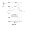
第5B圖是第5A圖的示例性的RF設備500與沒有任何短截線的RF設備的隔離圖的比較圖,圖中示出了天線間的隔離的改善。隔離圖中的參數S215表示從發射機天線510傳送到接收機天線520的功率。曲線542示出了RF設備500的隔離性能。除了在大約78GHz的存在槽/凹口之外,在超過80GHz後曲線542繼續下降。因此,通過調整一個或多個短截線的取向,可以實現在多個頻率範圍內提高的隔離性能。FIG. 5B is a comparison diagram of the isolation diagram of the
第6A圖是示出根據一些實施例的RF設備600的俯視圖,RF設備600包括具有短截線624a的天線610和不具有短截線的天線620。第6B圖是RF設備600與沒有任何短截線的RF設備的隔離圖的比較圖。隔離圖中的參數S216表示從天線610傳輸到天線620的功率。曲線642示出了RF設備600的隔離性能。在相同的封裝尺寸下,相較於沒有任何短截線的RF設備,RF設備600可以提供大約3dB的平均改善。FIG. 6A is a top view showing an
第7圖示出了根據一些實施例的用於製造本發明所描述的RF設備的示例性方法700。方法700可以在步驟702開始,在步驟702,提供模製層內的晶片。在一些實施例中,模製層可以是用於包裝的模製化合物層。晶片的表面和模製層的表面可以位於同一平面上。在步驟704,可以在晶片的表面和模製層的表面上沉積第一再分配層。在步驟706,可以在第一再分配層中形成天線,接地端和導電跡線。在一些實施例中,可以通過蝕刻第一再分配層來形成天線,接地端和導電跡線。天線可以包括天線元件和饋線。饋線可以具有連接到第一末端的第一端,連接到第二末端的第二端和連接到天線元件的第三端。在一些實施例中,第一末端可以是晶片的第一輸出端,第二末端可以是晶片的第二輸出端。在一些實施例中,第一末端可以是接地端,而第二末端可以是晶片的輸出端。短截線可以包括一開放端和連接到地的端。Figure 7 shows an exemplary method 700 for manufacturing the RF device described in the present invention according to some embodiments. The method 700 may begin in
本文描述的設備和技術的各個方面可以單獨使用,或組合使用,或以前面描述中描述的實施例中未特別討論的各種佈置使用,因此在其應用中不限於細節和佈置在前述描述中闡述或在附圖中示出的部件。例如,在一個實施例中描述的方面可以以與其它實施例中描述的方面以任何方式組合。The various aspects of the devices and technologies described herein can be used alone, or in combination, or in various arrangements that are not specifically discussed in the embodiments described in the foregoing description, and therefore are not limited to the details and arrangements in their applications. As set forth in the foregoing description Or the parts shown in the drawings. For example, aspects described in one embodiment may be combined with aspects described in other embodiments in any manner.
術語“大約”,“基本上”和“約”可以用於在一些實施例中在目標值的±20%內的±20%內,在一些實施例中在目標值的±10%內±5%在一些實施例中為目標值的±2%,但在一些實施例中為目標值的±2%。The terms "about", "substantially" and "about" can be used in some embodiments within ±20% of the target value, and in some embodiments within ±10% of the target value. % Is ±2% of the target value in some embodiments, but ±2% of the target value in some embodiments.
申請專利範圍中用以修飾元件的“第一”、“第二”等序數詞的使用本身未暗示任何優先權、優先次序、各元件之間的先後次序、或所執行方法的時間次序,而僅用作標識來區分具有相同名稱(具有不同序數詞)的不同元件。以上所述僅為本發明之較佳實施例,凡依本發明申請專利範圍所做之均等變化與修飾,皆應屬本發明之涵蓋範圍。The use of ordinal numbers such as "first" and "second" used to modify elements in the scope of the patent application does not imply any priority, priority, order between elements, or chronological order of execution methods, and It is only used as an identifier to distinguish different elements with the same name (with different ordinal numbers). The foregoing descriptions are only preferred embodiments of the present invention, and all equivalent changes and modifications made in accordance with the scope of the patent application of the present invention shall fall within the scope of the present invention.
200:RF設備200: RF equipment
216:平面216: Plane
224:短截線224: Stub
202:晶片202: chip
204:模製層204: Molded layer
206,210,214:電介質層206, 210, 214: Dielectric layer
208,212:再分配層208, 212: Redistribution layer
218:焊球218: Solder Ball
220:金屬層220: Metal layer
222:PCB222: PCB
110:發射機天線110: Transmitter antenna
120:接收機天線120: receiver antenna
Claims (17)
Translated fromChineseApplications Claiming Priority (4)
| Application Number | Priority Date | Filing Date | Title |
|---|---|---|---|
| US201762506637P | 2017-05-16 | 2017-05-16 | |
| US62/506,637 | 2017-05-16 | ||
| US15/685,885 | 2017-08-24 | ||
| US15/685,885US10615494B2 (en) | 2016-09-08 | 2017-08-24 | Coupling reduction method for antennas in package |
Publications (2)
| Publication Number | Publication Date |
|---|---|
| TW201902155A TW201902155A (en) | 2019-01-01 |
| TWI702810Btrue TWI702810B (en) | 2020-08-21 |
Family
ID=64402692
Family Applications (1)
| Application Number | Title | Priority Date | Filing Date |
|---|---|---|---|
| TW106138260ATWI702810B (en) | 2017-05-16 | 2017-11-06 | Radio frequency device |
Country Status (2)
| Country | Link |
|---|---|
| CN (1) | CN108923813B (en) |
| TW (1) | TWI702810B (en) |
Citations (8)
| Publication number | Priority date | Publication date | Assignee | Title |
|---|---|---|---|---|
| US6097339A (en)* | 1998-02-23 | 2000-08-01 | Qualcomm Incorporated | Substrate antenna |
| US7973729B2 (en)* | 2006-08-08 | 2011-07-05 | Sensormatic Electronics, LLC | Thin-film EAS and RFID antennas |
| EP2416444A2 (en)* | 2010-07-15 | 2012-02-08 | Sony Ericsson Mobile Communications AB | Multiple-input multiple-output (MIMO) multi-band antennas with a conductive neutralization line for signal decoupling |
| US20120274532A1 (en)* | 2011-04-27 | 2012-11-01 | Fujitsu Component Limited | Antenna device and electronic device |
| US8866292B2 (en)* | 2012-10-19 | 2014-10-21 | Infineon Technologies Ag | Semiconductor packages with integrated antenna and methods of forming thereof |
| WO2015094835A1 (en)* | 2013-12-17 | 2015-06-25 | Amazon Technologies, Inc. | Multi-band antenna |
| US20150288061A1 (en)* | 2014-04-08 | 2015-10-08 | Microsoft Corporation | Capacitively-coupled isolator assembly |
| US20150295311A1 (en)* | 2014-04-15 | 2015-10-15 | Dockon Ag | Antenna system using capacitively coupled compound loop antennas with antenna isolation provision |
Family Cites Families (2)
| Publication number | Priority date | Publication date | Assignee | Title |
|---|---|---|---|---|
| US8278749B2 (en)* | 2009-01-30 | 2012-10-02 | Infineon Technologies Ag | Integrated antennas in wafer level package |
| JP5524579B2 (en)* | 2009-11-12 | 2014-06-18 | 三星電子株式会社 | ANTENNA DEVICE AND WIRELESS COMMUNICATION DEVICE HAVING THE SAME |
- 2017
- 2017-11-03CNCN201711074656.8Apatent/CN108923813B/enactiveActive
- 2017-11-06TWTW106138260Apatent/TWI702810B/enactive
Patent Citations (8)
| Publication number | Priority date | Publication date | Assignee | Title |
|---|---|---|---|---|
| US6097339A (en)* | 1998-02-23 | 2000-08-01 | Qualcomm Incorporated | Substrate antenna |
| US7973729B2 (en)* | 2006-08-08 | 2011-07-05 | Sensormatic Electronics, LLC | Thin-film EAS and RFID antennas |
| EP2416444A2 (en)* | 2010-07-15 | 2012-02-08 | Sony Ericsson Mobile Communications AB | Multiple-input multiple-output (MIMO) multi-band antennas with a conductive neutralization line for signal decoupling |
| US20120274532A1 (en)* | 2011-04-27 | 2012-11-01 | Fujitsu Component Limited | Antenna device and electronic device |
| US8866292B2 (en)* | 2012-10-19 | 2014-10-21 | Infineon Technologies Ag | Semiconductor packages with integrated antenna and methods of forming thereof |
| WO2015094835A1 (en)* | 2013-12-17 | 2015-06-25 | Amazon Technologies, Inc. | Multi-band antenna |
| US20150288061A1 (en)* | 2014-04-08 | 2015-10-08 | Microsoft Corporation | Capacitively-coupled isolator assembly |
| US20150295311A1 (en)* | 2014-04-15 | 2015-10-15 | Dockon Ag | Antenna system using capacitively coupled compound loop antennas with antenna isolation provision |
Also Published As
| Publication number | Publication date |
|---|---|
| CN108923813B (en) | 2020-11-27 |
| CN108923813A (en) | 2018-11-30 |
| TW201902155A (en) | 2019-01-01 |
Similar Documents
| Publication | Publication Date | Title |
|---|---|---|
| US20230024260A1 (en) | Antenna module and radio frequency apparatus including the same | |
| US9608313B2 (en) | On-chip waveguide feeder for millimeter wave ICS and feeding methods, and multiple input and output millimeter wave transceiver system using same | |
| US7444734B2 (en) | Apparatus and methods for constructing antennas using vias as radiating elements formed in a substrate | |
| KR100455498B1 (en) | Print antenna | |
| US7589686B2 (en) | Small ultra wideband antenna having unidirectional radiation pattern | |
| US9444135B2 (en) | Integrated circuit package | |
| US12095182B2 (en) | Circuit integrated antenna | |
| JP2014150526A (en) | Antenna assembly and communication device comprising the same | |
| CN108736153B (en) | Three-frequency low-profile patch antenna | |
| WO2019120077A1 (en) | Antenna, and communication device | |
| EP3293818B1 (en) | Coupling reduction method for antennas in package | |
| US20150349428A1 (en) | Antenna device | |
| WO2019223318A1 (en) | Indoor base station and pifa antenna thereof | |
| CN113131178B (en) | Direction-finding antenna, direction-finding antenna system and electronic equipment | |
| Liu et al. | Cost-effective surface-mount off-center-fed dipole antenna element and its array for 5G millimeter wave new radio applications | |
| TWI702810B (en) | Radio frequency device | |
| WO2021084705A1 (en) | Circuit integrated antenna | |
| TWI467853B (en) | Dual band antenna and wireless communication device using the same | |
| CN115842236A (en) | High-isolation collinear polarization full-duplex packaging antenna | |
| CN210379412U (en) | Antenna, antenna assembly and electronic equipment | |
| US11239560B2 (en) | Ultra wide band antenna | |
| WO2021204491A1 (en) | Antenna for sending and/or receiving electromagnetic signals | |
| CN216648606U (en) | Antenna structure | |
| US12062857B2 (en) | Three-dimensional antenna module | |
| Nakano et al. | 60-GHz post-wall waveguide aperture antenna with directors made by multilayer PCB process |