TWI699953B - Control chip, DC-DC converter and portable electronic device using the DC-DC converter - Google Patents
Control chip, DC-DC converter and portable electronic device using the DC-DC converterDownload PDFInfo
- Publication number
- TWI699953B TWI699953BTW108145876ATW108145876ATWI699953BTW I699953 BTWI699953 BTW I699953BTW 108145876 ATW108145876 ATW 108145876ATW 108145876 ATW108145876 ATW 108145876ATW I699953 BTWI699953 BTW I699953B
- Authority
- TW
- Taiwan
- Prior art keywords
- signal
- voltage
- unit
- sum
- current
- Prior art date
Links
Images


Classifications
- Y—GENERAL TAGGING OF NEW TECHNOLOGICAL DEVELOPMENTS; GENERAL TAGGING OF CROSS-SECTIONAL TECHNOLOGIES SPANNING OVER SEVERAL SECTIONS OF THE IPC; TECHNICAL SUBJECTS COVERED BY FORMER USPC CROSS-REFERENCE ART COLLECTIONS [XRACs] AND DIGESTS
- Y02—TECHNOLOGIES OR APPLICATIONS FOR MITIGATION OR ADAPTATION AGAINST CLIMATE CHANGE
- Y02B—CLIMATE CHANGE MITIGATION TECHNOLOGIES RELATED TO BUILDINGS, e.g. HOUSING, HOUSE APPLIANCES OR RELATED END-USER APPLICATIONS
- Y02B70/00—Technologies for an efficient end-user side electric power management and consumption
- Y02B70/10—Technologies improving the efficiency by using switched-mode power supplies [SMPS], i.e. efficient power electronics conversion e.g. power factor correction or reduction of losses in power supplies or efficient standby modes
Landscapes
- Dc-Dc Converters (AREA)
Abstract
Translated fromChineseDescription
Translated fromChinese本發明係有關一種直流-直流轉換器,尤指一種可加速反應線電壓變化的直流-直流轉換器。The present invention relates to a DC-DC converter, in particular to a DC-DC converter capable of accelerating response to line voltage changes.
由於現今以DC-DC(direct current-direct current;直流-直流)輸出作為電源的電子產品對DC-DC的輸出精度和紋波要求越來越高,相對應的對DC-DC的負載瞬間變化(load-transient)和線電壓瞬間變化(line-transient)的 回應要求也提高。當DC-DC的負載電流突變或者輸入電壓突變時,DC-DC的輸出電壓紋波要盡可能小。As electronic products that use DC-DC (direct current-direct current; DC-DC) output as their power source are increasingly demanding DC-DC output accuracy and ripple, the corresponding DC-DC load changes instantaneously. Response requirements for load-transient and line-transient changes have also increased. When the DC-DC load current suddenly changes or the input voltage changes suddenly, the DC-DC output voltage ripple should be as small as possible.
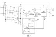
請參照圖1,其繪示一習知DC-DC轉換器的電路圖。如圖1 所示,該習知DC-DC轉換器具有由一電阻11a和一電阻11b串聯而成之一分壓電路、一誤差放大器12、一斜坡補償單元13、一電流感測單元14、一加法單元15、一比較器16、一驅動單元17、一電能傳輸單元18及一輸出電容19。Please refer to FIG. 1, which shows a circuit diagram of a conventional DC-DC converter. As shown in FIG. 1, the conventional DC-DC converter has a
該分壓電路係用以依一輸出電壓VOUT之一比例產生一回授電壓VFB;The voltage divider circuit is used to generate a feedback voltage VFB according to a proportion of an output voltage VOUT ;
誤差放大器12係用以對回授電壓VFB和一參考電壓VREF之一差值信號進行一積分操作以產生一誤差積分信號VEA;The
斜坡補償單元13係用以產生一斜坡補償信號VRAMP;The
電流感測單元14係用以依電能傳輸單元18之一電感電流IL產生一電流感測電壓VS;The
加法單元15係用以依斜坡補償信號VRAMP及電流感測電壓VS之和產生一加總信號VSUM;The
比較器16係用以對誤差積分信號VEA和加總信號VSUM進行一電壓比較操作以產生一脈衝寬度調變信號PWM;The
驅動單元17係用以依脈衝寬度調變信號PWM產生一驅動信號VDRV;The
電能傳輸單元18係用以依驅動信號VDRV之驅動進行一能量轉移操作以將一輸入電壓VIN之電能傳輸至輸出電壓VOUT,且在該能量轉移操作的過程中會產生電感電流IL;以及The
輸出電容19係用以對輸出電壓VOUT提供一濾波作用。The
於操作時,該習知DC-DC轉換器係通過電流感測單元14對電能傳輸單元18中流過一功率電晶體(未示於圖1中)的電感電流IL進行採樣以得到電流感測電壓VS; 在VS上疊加斜坡補償信號VRAMP以生成電壓加總信號VSUM;以及VSUM與電壓控制環路中的誤差放大器12所輸出的誤差積分信號VEA進行比較以產生脈衝寬度調變信號PWM。於穩態時,脈衝寬度調變信號PWM會具有一占空比D以使輸出電壓VOUT等於一預期的輸出電壓VO,其中VO= (1+R1/R2)*VREF,R1、R2分別代表電阻11a和電阻11b的電阻值。In operation, the conventional DC-DC converter uses the
當輸入電壓VIN的準位發生改變時,脈衝寬度調變信號PWM的占空比D須做出相應的改變以使輸出電壓VOUT能夠維持預期的輸出電壓VO。When the level of the input voltage VIN changes, the duty cycle D of the pulse width modulation signal PWM must be changed accordingly so that the output voltage VOUT can maintain the expected output voltage VO.
然而,占空比D卻會因誤差放大器12的積分電路的作用而不能加速變化到預期的值,從而導致輸出電壓VOUT出現抖動,且占空比D的變化速度越慢,輸出電壓VOUT的抖動就越大。However, the duty cycle D cannot be accelerated to the expected value due to the action of the integrator circuit of the
為解決上述問題,本領域亟需一種可加速反應線電壓變化的直流-直流轉換器。In order to solve the above-mentioned problems, there is an urgent need in the art for a DC-DC converter that can accelerate the response to line voltage changes.
本發明之一目的在於提供一種直流-直流轉換器,其可藉由將輸入電壓的變化量納入脈衝寬度調變信號的決定因子中以加速調整脈衝調變信號的占空比,從而除了使輸出電壓維持預期的電壓外,輸出電壓的漣波也能夠保持不變。One object of the present invention is to provide a DC-DC converter, which can accelerate the adjustment of the duty cycle of the pulse width modulation signal by incorporating the variation of the input voltage into the determinant factor of the pulse width modulation signal, so as to increase the output In addition to maintaining the expected voltage, the ripple of the output voltage can also remain unchanged.
本發明之另一目的在於提供一種攜帶型電子裝置,其可在兩種不同電壓的電壓源中任意擇一做為供電來源,且可藉由一可加速反應線電壓變化的直流-直流轉換器加速調整脈衝調變信號的占空比,以在電壓源切換時使輸出電壓維持預期的電壓及使輸出電壓的漣波保持不變,從而確保攜帶型電子裝置內之資訊處理單元能穩定操作。Another object of the present invention is to provide a portable electronic device, which can choose one of two voltage sources with different voltages as a power source, and can use a DC-DC converter that can accelerate the reaction of line voltage changes Accelerate the adjustment of the duty cycle of the pulse modulation signal to keep the output voltage at the expected voltage and the ripple of the output voltage when the voltage source is switched, so as to ensure the stable operation of the information processing unit in the portable electronic device.
為達到前述之目的,一種可加速反應線電壓變化的直流-直流轉換器乃被提出,其具有一控制電路以執行一直流-直流轉換操作,該直流-直流轉換操作係依一加總信號及一補償信號進行一電壓比較操作以產生一脈衝寬度調變信號,以將一輸入電壓轉成一輸出電壓,其中該加總信號係一斜坡補償信號與一電流感測電壓之和,該斜坡補償信號係一周期性的斜坡信號,且該電流感測電壓係一電能傳輸單元之一電感電流之感測值,該直流-直流轉換操作的特徵在於:In order to achieve the aforementioned purpose, a DC-DC converter that can accelerate the reaction of line voltage changes is proposed. It has a control circuit to perform a DC-DC conversion operation. The DC-DC conversion operation is based on a summing signal and A compensation signal performs a voltage comparison operation to generate a pulse width modulation signal to convert an input voltage into an output voltage, wherein the sum signal is the sum of a slope compensation signal and a current sense voltage, and the slope compensation The signal is a periodic ramp signal, and the current sensing voltage is a sensed value of an inductor current of an electric power transmission unit. The characteristics of the DC-DC conversion operation are:
該補償信號係一誤差積分信號與一輸入電壓感測信號之和,其中,該誤差積分信號係通過對一回授電壓和一參考電壓之一差值進行一積分操作而產生,該回授電壓係依該輸出電壓之一比例產生,且該輸入電壓感測信號係依該輸入電壓之一比例產生。The compensation signal is the sum of an error integration signal and an input voltage sensing signal, wherein the error integration signal is generated by performing an integration operation on a difference between a feedback voltage and a reference voltage, the feedback voltage It is generated according to a ratio of the output voltage, and the input voltage sensing signal is generated according to a ratio of the input voltage.
在一實施例中,所述控制電路具有一輸入電壓感測單元以產生該輸入電壓感測信號,且該輸入電壓感測單元包含一轉導放大器。In one embodiment, the control circuit has an input voltage sensing unit to generate the input voltage sensing signal, and the input voltage sensing unit includes a transconductance amplifier.
在一實施例中,所述控制電路具有一加法單元以依該誤差積分信號及該輸入電壓感測信號之和產生該補償信號,且該第一加法單元包含一NMOS電晶體及與該NMOS電晶體之源極疊接之一電阻。In one embodiment, the control circuit has an adding unit to generate the compensation signal according to the sum of the error integration signal and the input voltage sensing signal, and the first adding unit includes an NMOS transistor and the NMOS transistor. The source of the crystal is stacked with a resistor.
在一實施例中,所述控制電路具有一斜坡信號產生單元以產生該加總信號,該斜坡信號產生單元具有:In one embodiment, the control circuit has a ramp signal generating unit to generate the sum signal, and the ramp signal generating unit has:
一斜坡補償單元,用以產生該斜坡補償信號;A slope compensation unit for generating the slope compensation signal;
一電流感測單元,用以產生該電流感測電壓;以及A current sensing unit for generating the current sensing voltage; and
一加法單元,用以依該斜坡補償信號與該電流感測電壓之和產生該加總信號。An adding unit is used to generate the sum signal according to the sum of the slope compensation signal and the current sensing voltage.
在一實施例中,所述控制電路具有一斜坡信號產生單元以產生該加總信號,該斜坡信號產生單元具有:In one embodiment, the control circuit has a ramp signal generating unit to generate the sum signal, and the ramp signal generating unit has:
一電流源,其係由一直流電壓供電以輸出一定電流;A current source, which is powered by a DC voltage to output a certain current;
一電容,具有一上電極和一下電極,該上電極係與該電流源耦接且係用以提供該加總信號,該下電極係與該電能傳輸單元耦接以接收流出該電能傳輸單元的所述電感電流;A capacitor has an upper electrode and a lower electrode, the upper electrode is coupled to the current source and used to provide the summation signal, and the lower electrode is coupled to the power transmission unit to receive output from the power transmission unit The inductor current;
一開關,係與該電容並聯;以及A switch connected in parallel with the capacitor; and
一電阻,耦接於該下電極與一參考地之間。A resistor is coupled between the bottom electrode and a reference ground.
在一實施例中,所述控制電路具有一斜坡信號產生單元以產生該加總信號,該斜坡信號產生單元具有:In one embodiment, the control circuit has a ramp signal generating unit to generate the sum signal, and the ramp signal generating unit has:
一電容,具有一上電極和一下電極;A capacitor with an upper electrode and a lower electrode;
一第一開關,耦接於該上電極與一直流電壓之間;A first switch, coupled between the upper electrode and the DC voltage;
一第二開關,耦接於該下電極與該直流電壓之間;A second switch, coupled between the lower electrode and the DC voltage;
一電阻,其一端係與該下電極耦接,另一端係與該電能傳輸單元耦接以產生流入該電能傳輸單元的所述電感電流且係用以提供該加總信號;以及A resistor, one end of which is coupled to the lower electrode, and the other end of which is coupled to the power transmission unit to generate the inductive current flowing into the power transmission unit and to provide the sum signal; and
一電流源,其係耦接於該下電極與一參考地之間以提供流入該參考地之一定電流。A current source is coupled between the bottom electrode and a reference ground to provide a certain current flowing into the reference ground.
為達到前述之目的,本發明進一步提出一種控制晶片,其具有如前述之控制電路。In order to achieve the aforementioned objective, the present invention further provides a control chip having the aforementioned control circuit.
為達到前述之目的,本發明進一步提出一種攜帶型電子裝置,其具有如前述之可加速反應線電壓變化的直流-直流轉換器及一資訊處理單元,其中,所述之直流-直流轉換器係用以提供該輸出電壓以供電給該資訊處理單元。In order to achieve the foregoing objective, the present invention further provides a portable electronic device, which has the aforementioned DC-DC converter and an information processing unit capable of accelerating the response line voltage change, wherein the DC-DC converter is Used to provide the output voltage to power the information processing unit.
在可能的實施例中,所述之攜帶型電子裝置可為一攜帶型電腦或一手持智慧裝置。In a possible embodiment, the portable electronic device can be a portable computer or a handheld smart device.
本發明之直流-直流轉換器的輸出電壓能夠加速反應輸入電壓的準位變換的原理在於:本發明將輸入電壓的變化量納入脈衝寬度調變信號的決定因子中,依此,當輸入電壓從一第一準位變到一第二準位時,輸入電壓的變化會驅使脈衝寬度調變信號加速改變其占空比,且在穩態時,斜坡補償信號的變化量和電流感測電壓的變化量的總和會與輸入電壓的變化量成零和的關係,從而使誤差放大器的輸出準位不變,亦即使輸出電壓的漣波不變。The principle that the output voltage of the DC-DC converter of the present invention can accelerate the level change of the response input voltage is: the present invention incorporates the variation of the input voltage into the determining factor of the pulse width modulation signal, and accordingly, when the input voltage changes from When a first level is changed to a second level, the change of the input voltage will drive the pulse width modulation signal to accelerate to change its duty cycle, and in the steady state, the change of the slope compensation signal and the current sensing voltage The sum of the changes will have a zero-sum relationship with the change of the input voltage, so that the output level of the error amplifier remains unchanged, even if the ripple of the output voltage does not change.
請參照圖2,其為本發明之可加速反應線電壓變化的直流-直流轉換器之一實施例的電路圖。如圖2所示,該直流-直流轉換器具有一回授電路101、一誤差放大器102、一輸入電壓感測單元103、一第一加法單元104、一斜坡信號產生單元105、一比較器106、一驅動單元107、一電能傳輸單元108及一輸出電容109,其中,誤差放大器102、輸入電壓感測單元103、第一加法單元104、斜坡信號產生單元105、比較器106及驅動單元107組成一控制電路以執行一直流-直流轉換操作,且斜坡信號產生單元105具有一斜坡補償單元105a、一電流感測單元105b及一第二加法單元105c。Please refer to FIG. 2, which is a circuit diagram of an embodiment of the DC-DC converter capable of accelerating response to line voltage changes according to the present invention. As shown in FIG. 2, the DC-DC converter has a
回授電路101係用以依一輸出電壓VOUT之一比例產生一回授電壓VFB;The
誤差放大器102係用以對回授電壓VFB和一參考電壓(未示於圖2中)之一差值信號進行一積分操作以產生一誤差積分信號VEA;The
輸入電壓感測單元103係用以依一輸入電壓VIN之一比例產生一輸入電壓感測信號VINS;The input
第一加法單元104係用以依誤差積分信號VEA及輸入電壓感測信號VINS之和產生一補償信號VCOMP;The first adding
斜坡補償單元105a係用以產生一斜坡補償信號VRAMP;The
電流感測單元105b係用以依電能傳輸單元108之一電感電流IL產生一電流感測電壓VS;The
第二加法單元105c係用以依斜坡補償信號VRAMP及電流感測電壓VS之和產生一加總信號VSUM;The second adding
比較器106係用以對補償信號VCOMP和加總信號VSUM進行一電壓比較操作以產生一脈衝寬度調變信號PWM;The
驅動單元107係用以依脈衝寬度調變信號PWM產生一驅動信號VDRV;The
電能傳輸單元108係用以依驅動信號VDRV之驅動進行一能量轉移操作以將輸入電壓VIN之電能傳輸至輸出電壓VOUT,且在該能量轉移操作的過程中會產生電感電流IL;以及The
輸出電容109係用以對輸出電壓VOUT提供一濾波作用。The
於操作時,本發明之可加速反應線電壓變化的直流-直流轉換器係通過電流感測單元105b對電能傳輸單元108中流過一功率電晶體(未示於圖2中)的電感電流IL進行採樣以得到電流感測電壓VS; 在VS上疊加斜坡補償信號VRAMP以生成加總信號VSUM;以及VSUM與補償信號VCOMP進行比較以產生脈衝寬度調變信號PWM。於穩態時,脈衝寬度調變信號PWM會具有一占空比D以使輸出電壓VOUT等於一預期的輸出電壓VO,其中VO= (1+R1/R2)*VREF,R1、R2分別代表回授電路101中之兩個分壓電阻的電阻值,且VREF代表誤差放大器102內部之所述參考電壓。In operation, the DC-DC converter capable of accelerating the reaction of line voltage changes of the present invention uses the
當輸入電壓VIN的準位發生改變時,脈衝寬度調變信號PWM的占空比D須做出相應的改變以使輸出電壓VOUT能夠維持預期的輸出電壓VO。為了使輸出電壓VOUT的漣波能夠保持不變,占空比D的變化就不能由誤差積分信號VEA驅動。因此,本發明乃藉由將誤差積分信號VEA與輸入電壓感測信號VINS加總以產生補償信號VCOMP,以在電壓感測信號VINS的準位改變時能夠加速改變占空比D,再藉著整個電路的負回授機制驅使加總信號VSUM(電流感測電壓VS與斜坡補償信號VRAMP之加總)產生對應的變化量,從而除了使輸出電壓VOUT維持預期的輸出電壓VO外,誤差積分信號VEA也能維持不變,亦即輸出電壓VOUT的漣波也能夠保持不變。When the level of the input voltage VIN changes, the duty cycle D of the pulse width modulation signal PWM must be changed accordingly so that the output voltage VOUT can maintain the expected output voltage VO. In order to keep the ripple of the output voltage VOUT constant, the change of the duty cycle D cannot be driven by the error integration signal VEA . Therefore, the present invention generates the compensation signal VCOMP by adding the error integration signal VEA and the input voltage sensing signal VINS to accelerate the change of the duty cycle D when the level of the voltage sensing signal VINS changes. , And then use the negative feedback mechanism of the entire circuit to drive the sum signal VSUM (the sum of the current sense voltage VS and the slope compensation signal VRAMP ) to produce a corresponding amount of change, so as to maintain the expected output voltage VOUT In addition to the output voltage VO , the error integration signal VEA can also remain unchanged, that is, the ripple of the output voltage VOUT can also remain unchanged.
請參照圖3,其為圖2之可加速反應線電壓變化的直流-直流轉換器之一細部實施例的電路圖。如圖3所示,回授電路101具有成串聯組態之一第一電阻101a及一第二電阻101b;誤差放大器102係由內部具有一電阻-電容之低通網路的一積分放大器102a構成;輸入電壓感測單元103係由一轉導放大器103a構成,其中轉導放大器103a之正輸入端係與輸入電壓VIN耦接,負輸入端係與一參考地耦接,及輸出端係用以輸出一電流IVIN;第一加法單元104係由一NMOS電晶體104a和一第三電阻104b之一疊接組態構成;斜坡信號產生單元105中的斜坡補償單元105a、電流感測單元105b及第二加法單元105c的等效電路可由一電流源105d、一電容105e、一開關105f及一第四電阻105g構成,其中電流源105d、電容105e及開關105f係用以在電容105e的上、下電極間產生斜坡補償信號VRAMP,且第四電阻105g係用以依電感電流IL的峰值產生電流感測電壓VS,俾以在電容105e的上電極產生加總信號VSUM。具體而言,電流源105d係由一直流電壓供電以輸出一定電流;電容105e具有一上電極和一下電極,該上電極係與電流源105d耦接且係用以提供加總信號VSUM,該下電極係與電能傳輸單元108耦接以接收流出電能傳輸單元108的電感電流IL;開關105f係與電容105e並聯;以及第四電阻105g係耦接於該下電極與參考地之間。Please refer to FIG. 3, which is a circuit diagram of a detailed embodiment of the DC-DC converter capable of accelerating response to line voltage changes in FIG. 2. As shown in FIG. 3, the
於操作時,如果輸入電壓VIN由VIN1變為VIN2,也就是說


請參照圖4,其為圖2之可加速反應線電壓變化的直流-直流轉換器之另一細部實施例的電路圖。如圖4所示,回授電路101具有成串聯組態之一第一電阻101a及一第二電阻101b;誤差放大器102係由內部具有一電阻-電容之低通網路的一積分放大器102a構成;輸入電壓感測單元103係由一轉導放大器103a構成,其中轉導放大器103a之負輸入端係與輸入電壓VIN耦接,正輸入端係與參考地耦接,及輸出端係用以提供一灌電流IVIN;第一加法單元104係由一NMOS電晶體104a和一第三電阻104b之一疊接組態構成,以在第三電阻104b之一端產生補償信號VCOMP;斜坡信號產生單元105中的斜坡補償單元105a、電流感測單元105b及第二加法單元105c的等效電路可由一電容105e、一開關105f、一第四電阻105g、一開關105h及一電流源105i構成,其中電容105e、開關105f、開關105h及電流源105i係用以在電容105e的上、下電極間產生斜坡補償信號VRAMP,且第四電阻105g係用以依電感電流IL的谷值產生電流感測電壓VS,俾以在第四電阻105g的一端產生加總信號VSUM。具體而言,電容105e具有一上電極和一下電極; 開關105h耦接於該上電極與一直流電壓VB之間;開關105f耦接於該下電極與直流電壓VB之間;第四電阻105g之一端係與該下電極耦接,另一端係與電能傳輸單元108耦接以產生流入電能傳輸單元108的電感電流IL且係用以提供加總信號VSUM;以及電流源105i係耦接於該下電極與參考地之間以提供流入參考地之一定電流。Please refer to FIG. 4, which is a circuit diagram of another detailed embodiment of the DC-DC converter capable of accelerating response to line voltage changes in FIG. As shown in FIG. 4, the
於操作時,如果輸入電壓VIN由VIN1變為VIN2,也就是說
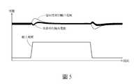
請參照圖5,其為依本發明之技術方案實現之一直流-直流轉換器和一習知直流-直流轉換器的工作波形對照圖。如圖5所示,本發明之輸出電壓的漣波明顯小於該習知直流-直流轉換器之輸出電壓的漣波。Please refer to FIG. 5, which is a comparison diagram of operating waveforms of a DC-DC converter and a conventional DC-DC converter according to the technical scheme of the present invention. As shown in FIG. 5, the output voltage ripple of the present invention is significantly smaller than the output voltage ripple of the conventional DC-DC converter.
依上述的說明,本發明可將上述的控制電路整合在一控制晶片中,且在可能的實施例中,該控制晶片可進一步將電能傳輸單元108中的功率電晶體整合進來。According to the above description, the present invention can integrate the above-mentioned control circuit into a control chip, and in a possible embodiment, the control chip can further integrate the power transistor in the
依上述的說明,本發明進一步提出一種攜帶型電子裝置。請參照圖6,其為本發明之攜帶型電子裝置之一實施例的方塊圖。如圖6所示,一攜帶型電子裝置200具有一直流-直流轉換器210及一資訊處理單元220,其中,直流-直流轉換器210係由前述之直流-直流轉換器實現以供電給資訊處理單元220,直流-直流轉換器210可將兩種不同準位的輸入電壓(VIN1, VIN2)轉成一輸出電壓VOUT,且在輸入電壓的準位切換(由開關211控制)過程中,該輸出電壓VOUT的漣波能夠維持在一預定的範圍內。所述兩種不同準位的輸入電壓可為兩個電池電壓或分別為一電池電壓及一交流-直流轉換器的直流輸出電壓。Based on the above description, the present invention further provides a portable electronic device. Please refer to FIG. 6, which is a block diagram of an embodiment of the portable electronic device of the present invention. As shown in FIG. 6, a portable
另外,攜帶型電子裝置200可為一攜帶型電腦或一手持智慧裝置。In addition, the portable
依上述的說明可知,本發明可提供以下的優點:According to the above description, the present invention can provide the following advantages:
1.本發明的直流-直流轉換器可藉由將輸入電壓的變化量納入脈衝寬度調變信號的決定因子中以加速調整脈衝調變信號的占空比,從而除了使輸出電壓維持預期的電壓外,輸出電壓的漣波也能夠保持不變。1. The DC-DC converter of the present invention can accelerate the adjustment of the duty cycle of the pulse width modulation signal by incorporating the variation of the input voltage into the determinant factor of the pulse width modulation signal, so as to keep the output voltage at the expected voltage In addition, the ripple of the output voltage can also remain unchanged.
2.本發明的攜帶型電子裝置可在兩種不同電壓的電壓源中任意擇一做為供電來源,且可藉由一可加速反應線電壓變化的直流-直流轉換器加速調整脈衝調變信號的占空比,以在電壓源切換時使輸出電壓維持預期的電壓及使輸出電壓的漣波保持不變,從而確保攜帶型電子裝置內之資訊處理單元能穩定操作。2. The portable electronic device of the present invention can choose one of two voltage sources with different voltages as the power supply source, and can accelerate the adjustment of the pulse modulation signal by a DC-DC converter that can accelerate the response to line voltage changes The duty cycle is to keep the output voltage at the expected voltage and the ripple of the output voltage when the voltage source is switched, so as to ensure the stable operation of the information processing unit in the portable electronic device.
本發明所揭示者,乃較佳實施例之一種,舉凡局部之變更或修飾而源於本發明之技術思想而為熟習該項技藝知人所易於推知者,俱不脫本發明之專利權範疇。The disclosure of the present invention is one of the preferred embodiments. Any partial changes or modifications that are derived from the technical ideas of the present invention and are easily inferred by those skilled in the art will not depart from the scope of the patent right of the present invention.
綜上所陳,本案無論目的、手段與功效,皆顯示其迥異於習知技術,且其首先發明合於實用,確實符合發明之專利要件,懇請 貴審查委員明察,並早日賜予專利俾嘉惠社會,是為至禱。To sum up, regardless of the purpose, means and effect of this case, it is shown that it is very different from the conventional technology, and its first invention is suitable for practicality, and it does meet the patent requirements of the invention. I implore the examiner to investigate and grant the patent as soon as possible. Society is for the best prayer.
11a:電阻11b:電阻12:誤差放大器13:斜坡補償單元14:電流感測單元15:加法單元16:比較器17:驅動單元18:電能傳輸單元19:輸出電容101:回授電路101a:第一電阻101b:第二電阻102:誤差放大器102a:積分放大器103:輸入電壓感測單元103a:轉導放大器104:第一加法單元104a:NMOS電晶體104b:第三電阻105:斜坡信號產生單元105a:斜坡補償單元105b:電流感測單元105c:第二加法單元105d:電流源105e:電容105f:開關105g:第四電阻105h:開關105i:電流源106:比較器107:驅動單元108:電能傳輸單元109:輸出電容200:攜帶型電子裝置210:直流-直流轉換器211:開關220:資訊處理單元11a:
圖1繪示一習知DC-DC轉換器的電路圖。 圖2為本發明之可加速反應線電壓變化的直流-直流轉換器之一實施例的電路圖。 圖3為圖2之可加速反應線電壓變化的直流-直流轉換器之一細部實施例的電路圖。 圖4為圖2之可加速反應線電壓變化的直流-直流轉換器之另一細部實施例的電路圖。 圖5為依本發明之技術方案實現之一直流-直流轉換器和一習知直流-直流轉換器的工作波形對照圖。 圖6為本發明之攜帶型電子裝置之一實施例的方塊圖。Figure 1 shows a circuit diagram of a conventional DC-DC converter. Fig. 2 is a circuit diagram of an embodiment of the DC-DC converter capable of accelerating response to line voltage changes according to the present invention. 3 is a circuit diagram of a detailed embodiment of the DC-DC converter capable of accelerating response to line voltage changes in FIG. 2. 4 is a circuit diagram of another detailed embodiment of the DC-DC converter capable of accelerating response to line voltage changes in FIG. 2. FIG. 5 is a comparison diagram of operating waveforms of a DC-DC converter and a conventional DC-DC converter implemented according to the technical scheme of the present invention. FIG. 6 is a block diagram of an embodiment of the portable electronic device of the invention.
101:回授電路101: feedback circuit
102:誤差放大器102: Error amplifier
103:輸入電壓感測單元103: Input voltage sensing unit
104:第一加法單元104: The first addition unit
105:斜坡信號產生單元105: ramp signal generation unit
105a:斜坡補償單元105a: slope compensation unit
105b:電流感測單元105b: Current sensing unit
105c:第二加法單元105c: second addition unit
106:比較器106: Comparator
107:驅動單元107: drive unit
108:電能傳輸單元108: Power Transmission Unit
109:輸出電容109: output capacitor
Claims (9)
Translated fromChinesePriority Applications (1)
| Application Number | Priority Date | Filing Date | Title |
|---|---|---|---|
| TW108145876ATWI699953B (en) | 2019-12-13 | 2019-12-13 | Control chip, DC-DC converter and portable electronic device using the DC-DC converter |
Applications Claiming Priority (1)
| Application Number | Priority Date | Filing Date | Title |
|---|---|---|---|
| TW108145876ATWI699953B (en) | 2019-12-13 | 2019-12-13 | Control chip, DC-DC converter and portable electronic device using the DC-DC converter |
Publications (2)
| Publication Number | Publication Date |
|---|---|
| TWI699953Btrue TWI699953B (en) | 2020-07-21 |
| TW202123589A TW202123589A (en) | 2021-06-16 |
Family
ID=72601999
Family Applications (1)
| Application Number | Title | Priority Date | Filing Date |
|---|---|---|---|
| TW108145876ATWI699953B (en) | 2019-12-13 | 2019-12-13 | Control chip, DC-DC converter and portable electronic device using the DC-DC converter |
Country Status (1)
| Country | Link |
|---|---|
| TW (1) | TWI699953B (en) |
Families Citing this family (1)
| Publication number | Priority date | Publication date | Assignee | Title |
|---|---|---|---|---|
| CN115001267A (en) | 2022-05-19 | 2022-09-02 | 昂宝电子(上海)有限公司 | Constant current switching power supply system, control chip and control method thereof |
Citations (6)
| Publication number | Priority date | Publication date | Assignee | Title |
|---|---|---|---|---|
| US7034586B2 (en)* | 2004-03-05 | 2006-04-25 | Intersil Americas Inc. | Startup circuit for converter with pre-biased load |
| US8710815B2 (en)* | 2010-06-25 | 2014-04-29 | Richtek Technology Corporation, R.O.C. | Adjustable voltage regulator with dynamic voltage compensation |
| US8742745B2 (en)* | 2011-07-27 | 2014-06-03 | Upi Semiconductor Corp. | DC-DC converter and voltage conversion method thereof |
| US8786270B2 (en)* | 2010-11-08 | 2014-07-22 | Intersil Americas Inc. | Synthetic ripple regulator with frequency control |
| TW201539957A (en)* | 2014-04-02 | 2015-10-16 | Green Solution Tech Co Ltd | Buck converter controller |
| TW201944711A (en)* | 2018-04-16 | 2019-11-16 | 來頡科技股份有限公司 | Power converter with adjustable ramp |
- 2019
- 2019-12-13TWTW108145876Apatent/TWI699953B/enactive
Patent Citations (6)
| Publication number | Priority date | Publication date | Assignee | Title |
|---|---|---|---|---|
| US7034586B2 (en)* | 2004-03-05 | 2006-04-25 | Intersil Americas Inc. | Startup circuit for converter with pre-biased load |
| US8710815B2 (en)* | 2010-06-25 | 2014-04-29 | Richtek Technology Corporation, R.O.C. | Adjustable voltage regulator with dynamic voltage compensation |
| US8786270B2 (en)* | 2010-11-08 | 2014-07-22 | Intersil Americas Inc. | Synthetic ripple regulator with frequency control |
| US8742745B2 (en)* | 2011-07-27 | 2014-06-03 | Upi Semiconductor Corp. | DC-DC converter and voltage conversion method thereof |
| TW201539957A (en)* | 2014-04-02 | 2015-10-16 | Green Solution Tech Co Ltd | Buck converter controller |
| TW201944711A (en)* | 2018-04-16 | 2019-11-16 | 來頡科技股份有限公司 | Power converter with adjustable ramp |
Also Published As
| Publication number | Publication date |
|---|---|
| TW202123589A (en) | 2021-06-16 |
Similar Documents
| Publication | Publication Date | Title |
|---|---|---|
| US9035640B2 (en) | High efficient control circuit for buck-boost converters and control method thereof | |
| TWI622260B (en) | Buck-boost converter with slope compensation, controller and control method thereof | |
| TWI397244B (en) | Buck converter with internal ripple compensation | |
| US7876073B2 (en) | Switching regulator with slope compensation and control method therefor | |
| CN100525031C (en) | Controller for a DC to DC converter having linear mode and switch mode capabilities | |
| TWI475346B (en) | Controller integrated circuit and method for switched mode regulator which converts input voltage to output voltage, and electronic device using the same | |
| US8525505B2 (en) | PWM controller and control method for a DC-DC voltage converter | |
| US8072195B2 (en) | Voltage converter | |
| CN104967328B (en) | System and method for the output current of regulation power supply transformation system | |
| Kim et al. | A noninverting buck–boost converter with state-based current control for Li-ion battery management in mobile applications | |
| WO2009139249A1 (en) | Current-mode control switching regulator and operations control method thereof | |
| CN102656787A (en) | Switching power supply circuit and power factor controller | |
| Zhang et al. | Analysis and implementation of a high-performance-integrated KY converter | |
| CN110692187B (en) | Control method and control circuit of switching power supply device | |
| US8742743B2 (en) | Switching control circuit | |
| US8686801B2 (en) | Power supply and DC-DC-conversion | |
| JP2013258798A (en) | Dc-dc conversion circuit | |
| CN102055336A (en) | Voltage boosting/lowering circuit | |
| TWI699953B (en) | Control chip, DC-DC converter and portable electronic device using the DC-DC converter | |
| CN110247547B (en) | Switching power converter and its controller circuit and control method | |
| TWI710204B (en) | Control chip, DC-DC converter and portable electronic device using the DC-DC converter | |
| CN115833582B (en) | Buck-boost converter, controller and control method thereof | |
| TW202112043A (en) | Step-up power converter that responds to variation of input voltage quickly and electronic device using same comprising an energy transfer unit, a ramp signal generation unit, an error-mean circuit, and a PWM signal generation unit | |
| CN109980959A (en) | Method and system based on the peak point current Operation switch power adapter by switch element | |
| CN112583257A (en) | Current mode DC-DC power converter and control method and controller thereof |