TWI699894B - Semiconductor device and display device including the semiconductor device - Google Patents
Semiconductor device and display device including the semiconductor deviceDownload PDFInfo
- Publication number
- TWI699894B TWI699894BTW105115500ATW105115500ATWI699894BTW I699894 BTWI699894 BTW I699894BTW 105115500 ATW105115500 ATW 105115500ATW 105115500 ATW105115500 ATW 105115500ATW I699894 BTWI699894 BTW I699894B
- Authority
- TW
- Taiwan
- Prior art keywords
- oxide semiconductor
- film
- transistor
- insulating film
- semiconductor film
- Prior art date
Links
- 239000004065semiconductorSubstances0.000titleclaimsabstractdescription609
- 229910052760oxygenInorganic materials0.000claimsdescription87
- 239000001301oxygenSubstances0.000claimsdescription87
- QVGXLLKOCUKJST-UHFFFAOYSA-Natomic oxygenChemical compound[O]QVGXLLKOCUKJST-UHFFFAOYSA-N0.000claimsdescription85
- 239000007789gasSubstances0.000claimsdescription71
- 239000013078crystalSubstances0.000claimsdescription66
- IJGRMHOSHXDMSA-UHFFFAOYSA-NAtomic nitrogenChemical compoundN#NIJGRMHOSHXDMSA-UHFFFAOYSA-N0.000claimsdescription40
- 229910052739hydrogenInorganic materials0.000claimsdescription35
- 239000001257hydrogenSubstances0.000claimsdescription31
- 229910052757nitrogenInorganic materials0.000claimsdescription20
- UFHFLCQGNIYNRP-UHFFFAOYSA-NHydrogenChemical compound[H][H]UFHFLCQGNIYNRP-UHFFFAOYSA-N0.000claimsdescription18
- 229910052782aluminiumInorganic materials0.000claimsdescription17
- 150000002431hydrogenChemical class0.000claimsdescription13
- OKTJSMMVPCPJKN-UHFFFAOYSA-NCarbonChemical compound[C]OKTJSMMVPCPJKN-UHFFFAOYSA-N0.000claimsdescription9
- 229910052799carbonInorganic materials0.000claimsdescription9
- 229910052738indiumInorganic materials0.000claimsdescription8
- 229910052733galliumInorganic materials0.000claimsdescription7
- 229910052796boronInorganic materials0.000claimsdescription6
- 229910052698phosphorusInorganic materials0.000claimsdescription6
- 239000011574phosphorusSubstances0.000claimsdescription6
- 229910052727yttriumInorganic materials0.000claimsdescription6
- ZOXJGFHDIHLPTG-UHFFFAOYSA-NBoronChemical compound[B]ZOXJGFHDIHLPTG-UHFFFAOYSA-N0.000claimsdescription5
- OAICVXFJPJFONN-UHFFFAOYSA-NPhosphorusChemical compound[P]OAICVXFJPJFONN-UHFFFAOYSA-N0.000claimsdescription5
- PXGOKWXKJXAPGV-UHFFFAOYSA-NFluorineChemical compoundFFPXGOKWXKJXAPGV-UHFFFAOYSA-N0.000claimsdescription4
- NINIDFKCEFEMDL-UHFFFAOYSA-NSulfurChemical compound[S]NINIDFKCEFEMDL-UHFFFAOYSA-N0.000claimsdescription4
- 229910052731fluorineInorganic materials0.000claimsdescription4
- 239000011737fluorineSubstances0.000claimsdescription4
- 239000011593sulfurSubstances0.000claimsdescription4
- 229910052717sulfurInorganic materials0.000claimsdescription4
- 229910052725zincInorganic materials0.000claimsdescription4
- 239000010408filmSubstances0.000description935
- 239000010410layerSubstances0.000description294
- 238000000034methodMethods0.000description114
- 239000000758substrateSubstances0.000description102
- 239000004973liquid crystal related substanceSubstances0.000description59
- 239000012535impuritySubstances0.000description56
- 230000006870functionEffects0.000description50
- 239000011701zincSubstances0.000description49
- 230000007547defectEffects0.000description40
- 125000004429atomChemical group0.000description37
- XUIMIQQOPSSXEZ-UHFFFAOYSA-NSiliconChemical compound[Si]XUIMIQQOPSSXEZ-UHFFFAOYSA-N0.000description34
- 229910052710siliconInorganic materials0.000description34
- 239000010703siliconSubstances0.000description34
- 238000010586diagramMethods0.000description30
- 238000004519manufacturing processMethods0.000description29
- 239000000463materialSubstances0.000description29
- 229910052751metalInorganic materials0.000description29
- 230000002829reductive effectEffects0.000description26
- 238000006243chemical reactionMethods0.000description24
- 238000012545processingMethods0.000description24
- 238000005401electroluminescenceMethods0.000description23
- 230000008569processEffects0.000description22
- 238000003860storageMethods0.000description21
- 239000002184metalSubstances0.000description20
- 239000002245particleSubstances0.000description19
- XKRFYHLGVUSROY-UHFFFAOYSA-NArgonChemical compound[Ar]XKRFYHLGVUSROY-UHFFFAOYSA-N0.000description18
- 230000000694effectsEffects0.000description18
- 238000004544sputter depositionMethods0.000description17
- -1for exampleSubstances0.000description15
- 238000010438heat treatmentMethods0.000description15
- XAGFODPZIPBFFR-UHFFFAOYSA-NaluminiumChemical group[Al]XAGFODPZIPBFFR-UHFFFAOYSA-N0.000description14
- 230000008859changeEffects0.000description14
- 229910052721tungstenInorganic materials0.000description14
- 229910044991metal oxideInorganic materials0.000description13
- 150000004706metal oxidesChemical class0.000description13
- 238000000623plasma-assisted chemical vapour depositionMethods0.000description13
- 239000010937tungstenSubstances0.000description13
- VYPSYNLAJGMNEJ-UHFFFAOYSA-NSilicium dioxideChemical compoundO=[Si]=OVYPSYNLAJGMNEJ-UHFFFAOYSA-N0.000description12
- 230000015572biosynthetic processEffects0.000description12
- 238000002173high-resolution transmission electron microscopyMethods0.000description12
- 229910052581Si3N4Inorganic materials0.000description11
- 230000007423decreaseEffects0.000description11
- 238000001312dry etchingMethods0.000description11
- 230000005669field effectEffects0.000description11
- 239000000203mixtureSubstances0.000description11
- 239000002159nanocrystalSubstances0.000description11
- HQVNEWCFYHHQES-UHFFFAOYSA-Nsilicon nitrideChemical compoundN12[Si]34N5[Si]62N3[Si]51N64HQVNEWCFYHHQES-UHFFFAOYSA-N0.000description11
- 239000002356single layerSubstances0.000description11
- WFKWXMTUELFFGS-UHFFFAOYSA-NtungstenChemical compound[W]WFKWXMTUELFFGS-UHFFFAOYSA-N0.000description11
- 238000003917TEM imageMethods0.000description10
- RTAQQCXQSZGOHL-UHFFFAOYSA-NTitaniumChemical compound[Ti]RTAQQCXQSZGOHL-UHFFFAOYSA-N0.000description10
- 230000005684electric fieldEffects0.000description10
- 238000010894electron beam technologyMethods0.000description10
- 229910052719titaniumInorganic materials0.000description10
- 239000010936titaniumSubstances0.000description10
- 229910052786argonInorganic materials0.000description9
- 239000012298atmosphereSubstances0.000description9
- 238000000231atomic layer depositionMethods0.000description9
- 229910052802copperInorganic materials0.000description9
- 239000010949copperSubstances0.000description9
- 229910052735hafniumInorganic materials0.000description9
- 229910052814silicon oxideInorganic materials0.000description9
- RYGMFSIKBFXOCR-UHFFFAOYSA-NCopperChemical compound[Cu]RYGMFSIKBFXOCR-UHFFFAOYSA-N0.000description8
- 239000003990capacitorSubstances0.000description8
- 239000000969carrierSubstances0.000description8
- 150000002500ionsChemical class0.000description8
- 150000004767nitridesChemical class0.000description8
- 238000000206photolithographyMethods0.000description8
- 238000005477sputtering targetMethods0.000description8
- 239000010409thin filmSubstances0.000description8
- 238000004458analytical methodMethods0.000description7
- 238000005229chemical vapour depositionMethods0.000description7
- 239000004020conductorSubstances0.000description7
- 238000000151depositionMethods0.000description7
- 230000008021depositionEffects0.000description7
- 239000005262ferroelectric liquid crystals (FLCs)Substances0.000description7
- 239000011261inert gasSubstances0.000description7
- 238000009413insulationMethods0.000description7
- 230000001590oxidative effectEffects0.000description7
- 229920001721polyimidePolymers0.000description7
- 238000002230thermal chemical vapour depositionMethods0.000description7
- XLYOFNOQVPJJNP-UHFFFAOYSA-NwaterSubstancesOXLYOFNOQVPJJNP-UHFFFAOYSA-N0.000description7
- 229910001868waterInorganic materials0.000description7
- XEEYBQQBJWHFJM-UHFFFAOYSA-NIronChemical compound[Fe]XEEYBQQBJWHFJM-UHFFFAOYSA-N0.000description6
- PXHVJJICTQNCMI-UHFFFAOYSA-NNickelChemical compound[Ni]PXHVJJICTQNCMI-UHFFFAOYSA-N0.000description6
- 238000009825accumulationMethods0.000description6
- 238000004891communicationMethods0.000description6
- VBJZVLUMGGDVMO-UHFFFAOYSA-Nhafnium atomChemical compound[Hf]VBJZVLUMGGDVMO-UHFFFAOYSA-N0.000description6
- 230000003287optical effectEffects0.000description6
- TWNQGVIAIRXVLR-UHFFFAOYSA-Noxo(oxoalumanyloxy)alumaneChemical compoundO=[Al]O[Al]=OTWNQGVIAIRXVLR-UHFFFAOYSA-N0.000description6
- 229910007541Zn OInorganic materials0.000description5
- 239000000956alloySubstances0.000description5
- 230000005540biological transmissionEffects0.000description5
- 238000000576coating methodMethods0.000description5
- 239000003086colorantSubstances0.000description5
- 238000002524electron diffraction dataMethods0.000description5
- 238000005530etchingMethods0.000description5
- 229910000449hafnium oxideInorganic materials0.000description5
- WIHZLLGSGQNAGK-UHFFFAOYSA-Nhafnium(4+);oxygen(2-)Chemical compound[O-2].[O-2].[Hf+4]WIHZLLGSGQNAGK-UHFFFAOYSA-N0.000description5
- APFVFJFRJDLVQX-UHFFFAOYSA-Nindium atomChemical compound[In]APFVFJFRJDLVQX-UHFFFAOYSA-N0.000description5
- 238000009832plasma treatmentMethods0.000description5
- 239000011347resinSubstances0.000description5
- 229920005989resinPolymers0.000description5
- 239000000565sealantSubstances0.000description5
- 239000000126substanceSubstances0.000description5
- 229910052718tinInorganic materials0.000description5
- 238000001039wet etchingMethods0.000description5
- 239000004925Acrylic resinSubstances0.000description4
- 229920000178Acrylic resinPolymers0.000description4
- GQPLMRYTRLFLPF-UHFFFAOYSA-NNitrous OxideChemical compound[O-][N+]#NGQPLMRYTRLFLPF-UHFFFAOYSA-N0.000description4
- BUGBHKTXTAQXES-UHFFFAOYSA-NSeleniumChemical compound[Se]BUGBHKTXTAQXES-UHFFFAOYSA-N0.000description4
- ATJFFYVFTNAWJD-UHFFFAOYSA-NTinChemical compound[Sn]ATJFFYVFTNAWJD-UHFFFAOYSA-N0.000description4
- 230000001133accelerationEffects0.000description4
- 229910052784alkaline earth metalInorganic materials0.000description4
- 229910045601alloyInorganic materials0.000description4
- 230000001186cumulative effectEffects0.000description4
- AJNVQOSZGJRYEI-UHFFFAOYSA-Ndigallium;oxygen(2-)Chemical compound[O-2].[O-2].[O-2].[Ga+3].[Ga+3]AJNVQOSZGJRYEI-UHFFFAOYSA-N0.000description4
- 238000007667floatingMethods0.000description4
- 229910001195gallium oxideInorganic materials0.000description4
- 239000011521glassSubstances0.000description4
- 238000005468ion implantationMethods0.000description4
- 239000000123paperSubstances0.000description4
- 230000003071parasitic effectEffects0.000description4
- 239000009719polyimide resinSubstances0.000description4
- 238000007639printingMethods0.000description4
- 238000002310reflectometryMethods0.000description4
- 230000002441reversible effectEffects0.000description4
- 238000001004secondary ion mass spectrometryMethods0.000description4
- 229910052711seleniumInorganic materials0.000description4
- 239000011669seleniumSubstances0.000description4
- UWCWUCKPEYNDNV-LBPRGKRZSA-N2,6-dimethyl-n-[[(2s)-pyrrolidin-2-yl]methyl]anilineChemical compoundCC1=CC=CC(C)=C1NC[C@H]1NCCC1UWCWUCKPEYNDNV-LBPRGKRZSA-N0.000description3
- VYZAMTAEIAYCRO-UHFFFAOYSA-NChromiumChemical compound[Cr]VYZAMTAEIAYCRO-UHFFFAOYSA-N0.000description3
- GYHNNYVSQQEPJS-UHFFFAOYSA-NGalliumChemical compound[Ga]GYHNNYVSQQEPJS-UHFFFAOYSA-N0.000description3
- PWHULOQIROXLJO-UHFFFAOYSA-NManganeseChemical compound[Mn]PWHULOQIROXLJO-UHFFFAOYSA-N0.000description3
- ZOKXTWBITQBERF-UHFFFAOYSA-NMolybdenumChemical compound[Mo]ZOKXTWBITQBERF-UHFFFAOYSA-N0.000description3
- 239000004983Polymer Dispersed Liquid CrystalSubstances0.000description3
- 229910052783alkali metalInorganic materials0.000description3
- 150000001340alkali metalsChemical class0.000description3
- 150000001342alkaline earth metalsChemical class0.000description3
- 239000002585baseSubstances0.000description3
- 238000005452bendingMethods0.000description3
- 230000000903blocking effectEffects0.000description3
- 229910052804chromiumInorganic materials0.000description3
- 239000011651chromiumSubstances0.000description3
- 150000001875compoundsChemical class0.000description3
- 230000003247decreasing effectEffects0.000description3
- 238000002003electron diffractionMethods0.000description3
- 238000001704evaporationMethods0.000description3
- 239000000835fiberSubstances0.000description3
- AMGQUBHHOARCQH-UHFFFAOYSA-Nindium;oxotinChemical compound[In].[Sn]=OAMGQUBHHOARCQH-UHFFFAOYSA-N0.000description3
- 229910010272inorganic materialInorganic materials0.000description3
- 239000011147inorganic materialSubstances0.000description3
- 229910052742ironInorganic materials0.000description3
- 239000007788liquidSubstances0.000description3
- 229910052748manganeseInorganic materials0.000description3
- 239000011572manganeseSubstances0.000description3
- 229910052750molybdenumInorganic materials0.000description3
- 239000011733molybdenumSubstances0.000description3
- 229910052759nickelInorganic materials0.000description3
- 239000011368organic materialSubstances0.000description3
- 150000001282organosilanesChemical class0.000description3
- 239000007800oxidant agentSubstances0.000description3
- 239000004033plasticSubstances0.000description3
- 229920003023plasticPolymers0.000description3
- 229920000728polyesterPolymers0.000description3
- 238000007789sealingMethods0.000description3
- 229910052709silverInorganic materials0.000description3
- 239000004332silverSubstances0.000description3
- 229910052715tantalumInorganic materials0.000description3
- GUVRBAGPIYLISA-UHFFFAOYSA-Ntantalum atomChemical compound[Ta]GUVRBAGPIYLISA-UHFFFAOYSA-N0.000description3
- JBQYATWDVHIOAR-UHFFFAOYSA-NtellanylidenegermaniumChemical compound[Te]=[Ge]JBQYATWDVHIOAR-UHFFFAOYSA-N0.000description3
- WZJUBBHODHNQPW-UHFFFAOYSA-N2,4,6,8-tetramethyl-1,3,5,7,2$l^{3},4$l^{3},6$l^{3},8$l^{3}-tetraoxatetrasilocaneChemical compoundC[Si]1O[Si](C)O[Si](C)O[Si](C)O1WZJUBBHODHNQPW-UHFFFAOYSA-N0.000description2
- JBRZTFJDHDCESZ-UHFFFAOYSA-NAsGaChemical compound[As]#[Ga]JBRZTFJDHDCESZ-UHFFFAOYSA-N0.000description2
- CURLTUGMZLYLDI-UHFFFAOYSA-NCarbon dioxideChemical compoundO=C=OCURLTUGMZLYLDI-UHFFFAOYSA-N0.000description2
- ZAMOUSCENKQFHK-UHFFFAOYSA-NChlorine atomChemical compound[Cl]ZAMOUSCENKQFHK-UHFFFAOYSA-N0.000description2
- ROSDSFDQCJNGOL-UHFFFAOYSA-NDimethylamineChemical compoundCNCROSDSFDQCJNGOL-UHFFFAOYSA-N0.000description2
- MYMOFIZGZYHOMD-UHFFFAOYSA-NDioxygenChemical compoundO=OMYMOFIZGZYHOMD-UHFFFAOYSA-N0.000description2
- 229910001218Gallium arsenideInorganic materials0.000description2
- BPQQTUXANYXVAA-UHFFFAOYSA-NOrthosilicateChemical compound[O-][Si]([O-])([O-])[O-]BPQQTUXANYXVAA-UHFFFAOYSA-N0.000description2
- CBENFWSGALASAD-UHFFFAOYSA-NOzoneChemical compound[O-][O+]=OCBENFWSGALASAD-UHFFFAOYSA-N0.000description2
- 239000004642PolyimideSubstances0.000description2
- 229910000577Silicon-germaniumInorganic materials0.000description2
- BOTDANWDWHJENH-UHFFFAOYSA-NTetraethyl orthosilicateChemical compoundCCO[Si](OCC)(OCC)OCCBOTDANWDWHJENH-UHFFFAOYSA-N0.000description2
- GWEVSGVZZGPLCZ-UHFFFAOYSA-NTitan oxideChemical compoundO=[Ti]=OGWEVSGVZZGPLCZ-UHFFFAOYSA-N0.000description2
- NRTOMJZYCJJWKI-UHFFFAOYSA-NTitanium nitrideChemical compound[Ti]#NNRTOMJZYCJJWKI-UHFFFAOYSA-N0.000description2
- 238000002441X-ray diffractionMethods0.000description2
- XLOMVQKBTHCTTD-UHFFFAOYSA-NZinc monoxideChemical compound[Zn]=OXLOMVQKBTHCTTD-UHFFFAOYSA-N0.000description2
- 230000004075alterationEffects0.000description2
- 239000004760aramidSubstances0.000description2
- 229920003235aromatic polyamidePolymers0.000description2
- 229910052800carbon group elementInorganic materials0.000description2
- 229910052801chlorineInorganic materials0.000description2
- 239000000460chlorineSubstances0.000description2
- HVYWMOMLDIMFJA-DPAQBDIFSA-NcholesterolChemical compoundC1C=C2C[C@@H](O)CC[C@]2(C)[C@@H]2[C@@H]1[C@@H]1CC[C@H]([C@H](C)CCCC(C)C)[C@@]1(C)CC2HVYWMOMLDIMFJA-DPAQBDIFSA-N0.000description2
- 229910017052cobaltInorganic materials0.000description2
- 239000010941cobaltSubstances0.000description2
- GUTLYIVDDKVIGB-UHFFFAOYSA-Ncobalt atomChemical compound[Co]GUTLYIVDDKVIGB-UHFFFAOYSA-N0.000description2
- PMHQVHHXPFUNSP-UHFFFAOYSA-Mcopper(1+);methylsulfanylmethane;bromideChemical compoundBr[Cu].CSCPMHQVHHXPFUNSP-UHFFFAOYSA-M0.000description2
- AXAZMDOAUQTMOW-UHFFFAOYSA-NdimethylzincChemical compoundC[Zn]CAXAZMDOAUQTMOW-UHFFFAOYSA-N0.000description2
- 229910001882dioxygenInorganic materials0.000description2
- 238000005516engineering processMethods0.000description2
- 230000001747exhibiting effectEffects0.000description2
- 239000011888foilSubstances0.000description2
- 239000001307heliumSubstances0.000description2
- 229910052734heliumInorganic materials0.000description2
- SWQJXJOGLNCZEY-UHFFFAOYSA-Nhelium atomChemical compound[He]SWQJXJOGLNCZEY-UHFFFAOYSA-N0.000description2
- 229910003437indium oxideInorganic materials0.000description2
- PJXISJQVUVHSOJ-UHFFFAOYSA-Nindium(iii) oxideChemical compound[O-2].[O-2].[O-2].[In+3].[In+3]PJXISJQVUVHSOJ-UHFFFAOYSA-N0.000description2
- 229910052743kryptonInorganic materials0.000description2
- DNNSSWSSYDEUBZ-UHFFFAOYSA-Nkrypton atomChemical compound[Kr]DNNSSWSSYDEUBZ-UHFFFAOYSA-N0.000description2
- 238000010030laminatingMethods0.000description2
- 230000014759maintenance of locationEffects0.000description2
- WPBNNNQJVZRUHP-UHFFFAOYSA-Lmanganese(2+);methyl n-[[2-(methoxycarbonylcarbamothioylamino)phenyl]carbamothioyl]carbamate;n-[2-(sulfidocarbothioylamino)ethyl]carbamodithioateChemical compound[Mn+2].[S-]C(=S)NCCNC([S-])=S.COC(=O)NC(=S)NC1=CC=CC=C1NC(=S)NC(=O)OCWPBNNNQJVZRUHP-UHFFFAOYSA-L0.000description2
- 238000002156mixingMethods0.000description2
- 229910052754neonInorganic materials0.000description2
- GKAOGPIIYCISHV-UHFFFAOYSA-Nneon atomChemical compound[Ne]GKAOGPIIYCISHV-UHFFFAOYSA-N0.000description2
- 239000001272nitrous oxideSubstances0.000description2
- QGLKJKCYBOYXKC-UHFFFAOYSA-NnonaoxidotritungstenChemical compoundO=[W]1(=O)O[W](=O)(=O)O[W](=O)(=O)O1QGLKJKCYBOYXKC-UHFFFAOYSA-N0.000description2
- HMMGMWAXVFQUOA-UHFFFAOYSA-NoctamethylcyclotetrasiloxaneChemical compoundC[Si]1(C)O[Si](C)(C)O[Si](C)(C)O[Si](C)(C)O1HMMGMWAXVFQUOA-UHFFFAOYSA-N0.000description2
- SIWVEOZUMHYXCS-UHFFFAOYSA-Noxo(oxoyttriooxy)yttriumChemical compoundO=[Y]O[Y]=OSIWVEOZUMHYXCS-UHFFFAOYSA-N0.000description2
- 230000000737periodic effectEffects0.000description2
- 230000000704physical effectEffects0.000description2
- 229910052696pnictogenInorganic materials0.000description2
- 229920000139polyethylene terephthalatePolymers0.000description2
- 239000005020polyethylene terephthalateSubstances0.000description2
- 229920000642polymerPolymers0.000description2
- 239000002243precursorSubstances0.000description2
- 230000001681protective effectEffects0.000description2
- 238000004098selected area electron diffractionMethods0.000description2
- 239000002904solventSubstances0.000description2
- 125000006850spacer groupChemical group0.000description2
- 239000010935stainless steelSubstances0.000description2
- 229910001220stainless steelInorganic materials0.000description2
- CZDYPVPMEAXLPK-UHFFFAOYSA-NtetramethylsilaneChemical compoundC[Si](C)(C)CCZDYPVPMEAXLPK-UHFFFAOYSA-N0.000description2
- OGIDPMRJRNCKJF-UHFFFAOYSA-Ntitanium oxideInorganic materials[Ti]=OOGIDPMRJRNCKJF-UHFFFAOYSA-N0.000description2
- 229910052723transition metalInorganic materials0.000description2
- XCZXGTMEAKBVPV-UHFFFAOYSA-NtrimethylgalliumChemical compoundC[Ga](C)CXCZXGTMEAKBVPV-UHFFFAOYSA-N0.000description2
- 229910001930tungsten oxideInorganic materials0.000description2
- 229910052724xenonInorganic materials0.000description2
- FHNFHKCVQCLJFQ-UHFFFAOYSA-Nxenon atomChemical compound[Xe]FHNFHKCVQCLJFQ-UHFFFAOYSA-N0.000description2
- VWQVUPCCIRVNHF-UHFFFAOYSA-Nyttrium atomChemical compound[Y]VWQVUPCCIRVNHF-UHFFFAOYSA-N0.000description2
- YVTHLONGBIQYBO-UHFFFAOYSA-Nzinc indium(3+) oxygen(2-)Chemical compound[O--].[Zn++].[In+3]YVTHLONGBIQYBO-UHFFFAOYSA-N0.000description2
- MGWGWNFMUOTEHG-UHFFFAOYSA-N4-(3,5-dimethylphenyl)-1,3-thiazol-2-amineChemical compoundCC1=CC(C)=CC(C=2N=C(N)SC=2)=C1MGWGWNFMUOTEHG-UHFFFAOYSA-N0.000description1
- 244000025254Cannabis sativaSpecies0.000description1
- 235000012766Cannabis sativa ssp. sativa var. sativaNutrition0.000description1
- 235000012765Cannabis sativa ssp. sativa var. spontaneaNutrition0.000description1
- 229920000298CellophanePolymers0.000description1
- 239000004986Cholesteric liquid crystals (ChLC)Substances0.000description1
- 229920000742CottonPolymers0.000description1
- 239000004593EpoxySubstances0.000description1
- 229910004129HfSiOInorganic materials0.000description1
- 239000005264High molar mass liquid crystalSubstances0.000description1
- DGAQECJNVWCQMB-PUAWFVPOSA-MIlexoside XXIXChemical compoundC[C@@H]1CC[C@@]2(CC[C@@]3(C(=CC[C@H]4[C@]3(CC[C@@H]5[C@@]4(CC[C@@H](C5(C)C)OS(=O)(=O)[O-])C)C)[C@@H]2[C@]1(C)O)C)C(=O)O[C@H]6[C@@H]([C@H]([C@@H]([C@H](O6)CO)O)O)O.[Na+]DGAQECJNVWCQMB-PUAWFVPOSA-M0.000description1
- WHXSMMKQMYFTQS-UHFFFAOYSA-NLithiumChemical compound[Li]WHXSMMKQMYFTQS-UHFFFAOYSA-N0.000description1
- 229910052779NeodymiumInorganic materials0.000description1
- 239000004677NylonSubstances0.000description1
- 239000004952PolyamideSubstances0.000description1
- 239000004721Polyphenylene oxideSubstances0.000description1
- 239000004743PolypropyleneSubstances0.000description1
- BLRPTPMANUNPDV-UHFFFAOYSA-NSilaneChemical compound[SiH4]BLRPTPMANUNPDV-UHFFFAOYSA-N0.000description1
- 239000004990Smectic liquid crystalSubstances0.000description1
- 229910008813Sn—SiInorganic materials0.000description1
- UCKMPCXJQFINFW-UHFFFAOYSA-NSulphideChemical compound[S-2]UCKMPCXJQFINFW-UHFFFAOYSA-N0.000description1
- 239000004974Thermotropic liquid crystalSubstances0.000description1
- 239000007983Tris bufferSubstances0.000description1
- HCHKCACWOHOZIP-UHFFFAOYSA-NZincChemical compound[Zn]HCHKCACWOHOZIP-UHFFFAOYSA-N0.000description1
- QCWXUUIWCKQGHC-UHFFFAOYSA-NZirconiumChemical compound[Zr]QCWXUUIWCKQGHC-UHFFFAOYSA-N0.000description1
- 229910009367Zn MInorganic materials0.000description1
- OLBVUFHMDRJKTK-UHFFFAOYSA-N[N].[O]Chemical compound[N].[O]OLBVUFHMDRJKTK-UHFFFAOYSA-N0.000description1
- LEVVHYCKPQWKOP-UHFFFAOYSA-N[Si].[Ge]Chemical compound[Si].[Ge]LEVVHYCKPQWKOP-UHFFFAOYSA-N0.000description1
- 229920006221acetate fiberPolymers0.000description1
- NIXOWILDQLNWCW-UHFFFAOYSA-Nacrylic acid groupChemical groupC(C=C)(=O)ONIXOWILDQLNWCW-UHFFFAOYSA-N0.000description1
- 239000005407aluminoborosilicate glassSubstances0.000description1
- 150000001408amidesChemical class0.000description1
- 229910021417amorphous siliconInorganic materials0.000description1
- 238000004380ashingMethods0.000description1
- 229910052788bariumInorganic materials0.000description1
- DSAJWYNOEDNPEQ-UHFFFAOYSA-Nbarium atomChemical compound[Ba]DSAJWYNOEDNPEQ-UHFFFAOYSA-N0.000description1
- 230000004888barrier functionEffects0.000description1
- 230000008901benefitEffects0.000description1
- UMIVXZPTRXBADB-UHFFFAOYSA-NbenzocyclobuteneChemical compoundC1=CC=C2CCC2=C1UMIVXZPTRXBADB-UHFFFAOYSA-N0.000description1
- 229910052795boron group elementInorganic materials0.000description1
- 239000005388borosilicate glassSubstances0.000description1
- 230000005587bubblingEffects0.000description1
- 235000009120camoNutrition0.000description1
- 229910002092carbon dioxideInorganic materials0.000description1
- 239000001569carbon dioxideSubstances0.000description1
- 239000012159carrier gasSubstances0.000description1
- 239000000919ceramicSubstances0.000description1
- 235000005607chanvre indienNutrition0.000description1
- 230000003098cholesteric effectEffects0.000description1
- 235000012000cholesterolNutrition0.000description1
- 239000011248coating agentSubstances0.000description1
- 239000002131composite materialSubstances0.000description1
- 238000011109contaminationMethods0.000description1
- 150000001879copperChemical class0.000description1
- 238000012937correctionMethods0.000description1
- 238000002425crystallisationMethods0.000description1
- 230000008025crystallizationEffects0.000description1
- 230000018044dehydrationEffects0.000description1
- 238000006297dehydration reactionMethods0.000description1
- 238000006356dehydrogenation reactionMethods0.000description1
- 238000011161developmentMethods0.000description1
- HQWPLXHWEZZGKY-UHFFFAOYSA-NdiethylzincChemical compoundCC[Zn]CCHQWPLXHWEZZGKY-UHFFFAOYSA-N0.000description1
- 238000009792diffusion processMethods0.000description1
- ZYLGGWPMIDHSEZ-UHFFFAOYSA-Ndimethylazanide;hafnium(4+)Chemical compound[Hf+4].C[N-]C.C[N-]C.C[N-]C.C[N-]CZYLGGWPMIDHSEZ-UHFFFAOYSA-N0.000description1
- 230000008034disappearanceEffects0.000description1
- 238000006073displacement reactionMethods0.000description1
- 229920001971elastomerPolymers0.000description1
- 230000005611electricityEffects0.000description1
- 239000003822epoxy resinSubstances0.000description1
- NPEOKFBCHNGLJD-UHFFFAOYSA-Nethyl(methyl)azanide;hafnium(4+)Chemical compound[Hf+4].CC[N-]C.CC[N-]C.CC[N-]C.CC[N-]CNPEOKFBCHNGLJD-UHFFFAOYSA-N0.000description1
- KCWYOFZQRFCIIE-UHFFFAOYSA-NethylsilaneChemical compoundCC[SiH3]KCWYOFZQRFCIIE-UHFFFAOYSA-N0.000description1
- 239000004744fabricSubstances0.000description1
- 239000002657fibrous materialSubstances0.000description1
- 238000002309gasificationMethods0.000description1
- 229910052732germaniumInorganic materials0.000description1
- GNPVGFCGXDBREM-UHFFFAOYSA-Ngermanium atomChemical compound[Ge]GNPVGFCGXDBREM-UHFFFAOYSA-N0.000description1
- 229910001385heavy metalInorganic materials0.000description1
- 239000011487hempSubstances0.000description1
- VHHHONWQHHHLTI-UHFFFAOYSA-NhexachloroethaneChemical compoundClC(Cl)(Cl)C(Cl)(Cl)ClVHHHONWQHHHLTI-UHFFFAOYSA-N0.000description1
- FFUAGWLWBBFQJT-UHFFFAOYSA-NhexamethyldisilazaneChemical compoundC[Si](C)(C)N[Si](C)(C)CFFUAGWLWBBFQJT-UHFFFAOYSA-N0.000description1
- 238000010191image analysisMethods0.000description1
- 238000003384imaging methodMethods0.000description1
- 238000010348incorporationMethods0.000description1
- 238000002347injectionMethods0.000description1
- 239000007924injectionSubstances0.000description1
- 230000010354integrationEffects0.000description1
- 238000000608laser ablationMethods0.000description1
- 239000010985leatherSubstances0.000description1
- 229910052744lithiumInorganic materials0.000description1
- 230000005389magnetismEffects0.000description1
- 230000007257malfunctionEffects0.000description1
- 239000011159matrix materialSubstances0.000description1
- 239000012528membraneSubstances0.000description1
- 229910001092metal group alloyInorganic materials0.000description1
- 229910021424microcrystalline siliconInorganic materials0.000description1
- 229910021421monocrystalline siliconInorganic materials0.000description1
- CUZHTAHNDRTVEF-UHFFFAOYSA-Nn-[bis(dimethylamino)alumanyl]-n-methylmethanamineChemical compound[Al+3].C[N-]C.C[N-]C.C[N-]CCUZHTAHNDRTVEF-UHFFFAOYSA-N0.000description1
- QEFYFXOXNSNQGX-UHFFFAOYSA-Nneodymium atomChemical compound[Nd]QEFYFXOXNSNQGX-UHFFFAOYSA-N0.000description1
- 230000006855networkingEffects0.000description1
- JCXJVPUVTGWSNB-UHFFFAOYSA-Nnitrogen dioxideInorganic materialsO=[N]=OJCXJVPUVTGWSNB-UHFFFAOYSA-N0.000description1
- 229920001778nylonPolymers0.000description1
- 230000001151other effectEffects0.000description1
- 230000003647oxidationEffects0.000description1
- 238000007254oxidation reactionMethods0.000description1
- 125000004430oxygen atomChemical groupO*0.000description1
- 230000003863physical functionEffects0.000description1
- 230000010287polarizationEffects0.000description1
- 229920002647polyamidePolymers0.000description1
- 229910021420polycrystalline siliconInorganic materials0.000description1
- 229920000647polyepoxidePolymers0.000description1
- 229920000570polyetherPolymers0.000description1
- 239000011112polyethylene naphthalateSubstances0.000description1
- 229920001155polypropylenePolymers0.000description1
- 229920001296polysiloxanePolymers0.000description1
- 229920002635polyurethanePolymers0.000description1
- 239000004814polyurethaneSubstances0.000description1
- 239000004800polyvinyl chlorideSubstances0.000description1
- 229920000915polyvinyl chloridePolymers0.000description1
- 229920002620polyvinyl fluoridePolymers0.000description1
- 238000010248power generationMethods0.000description1
- 238000003672processing methodMethods0.000description1
- 230000000750progressive effectEffects0.000description1
- UIDUKLCLJMXFEO-UHFFFAOYSA-NpropylsilaneChemical compoundCCC[SiH3]UIDUKLCLJMXFEO-UHFFFAOYSA-N0.000description1
- 239000002096quantum dotSubstances0.000description1
- 239000010453quartzSubstances0.000description1
- 230000005855radiationEffects0.000description1
- 150000003254radicalsChemical class0.000description1
- 230000006798recombinationEffects0.000description1
- 238000005215recombinationMethods0.000description1
- 230000004044responseEffects0.000description1
- 229910052706scandiumInorganic materials0.000description1
- SIXSYDAISGFNSX-UHFFFAOYSA-Nscandium atomChemical compound[Sc]SIXSYDAISGFNSX-UHFFFAOYSA-N0.000description1
- 229910000077silaneInorganic materials0.000description1
- 150000004756silanesChemical class0.000description1
- 239000000377silicon dioxideSubstances0.000description1
- 239000005361soda-lime glassSubstances0.000description1
- 229910052708sodiumInorganic materials0.000description1
- 239000011734sodiumSubstances0.000description1
- 238000004528spin coatingMethods0.000description1
- 239000003381stabilizerSubstances0.000description1
- 230000003068static effectEffects0.000description1
- 239000004575stoneSubstances0.000description1
- 238000012916structural analysisMethods0.000description1
- 238000006467substitution reactionMethods0.000description1
- 229920002994synthetic fiberPolymers0.000description1
- 239000012209synthetic fiberSubstances0.000description1
- 229920003002synthetic resinPolymers0.000description1
- 239000000057synthetic resinSubstances0.000description1
- 239000013077target materialSubstances0.000description1
- 238000012360testing methodMethods0.000description1
- XOLBLPGZBRYERU-UHFFFAOYSA-Ntin dioxideChemical compoundO=[Sn]=OXOLBLPGZBRYERU-UHFFFAOYSA-N0.000description1
- 229910001887tin oxideInorganic materials0.000description1
- 150000003624transition metalsChemical class0.000description1
- 238000002834transmittanceMethods0.000description1
- QQQSFSZALRVCSZ-UHFFFAOYSA-NtriethoxysilaneChemical compoundCCO[SiH](OCC)OCCQQQSFSZALRVCSZ-UHFFFAOYSA-N0.000description1
- RGGPNXQUMRMPRA-UHFFFAOYSA-NtriethylgalliumChemical compoundCC[Ga](CC)CCRGGPNXQUMRMPRA-UHFFFAOYSA-N0.000description1
- MCULRUJILOGHCJ-UHFFFAOYSA-NtriisobutylaluminiumChemical compoundCC(C)C[Al](CC(C)C)CC(C)CMCULRUJILOGHCJ-UHFFFAOYSA-N0.000description1
- JLTRXTDYQLMHGR-UHFFFAOYSA-NtrimethylaluminiumChemical compoundC[Al](C)CJLTRXTDYQLMHGR-UHFFFAOYSA-N0.000description1
- IBEFSUTVZWZJEL-UHFFFAOYSA-NtrimethylindiumChemical compoundC[In](C)CIBEFSUTVZWZJEL-UHFFFAOYSA-N0.000description1
- 150000003657tungstenChemical class0.000description1
- 238000001771vacuum depositionMethods0.000description1
- 238000007738vacuum evaporationMethods0.000description1
- 239000002023woodSubstances0.000description1
- 239000011787zinc oxideSubstances0.000description1
- 229910052726zirconiumInorganic materials0.000description1
Images


Classifications
- H—ELECTRICITY
- H10—SEMICONDUCTOR DEVICES; ELECTRIC SOLID-STATE DEVICES NOT OTHERWISE PROVIDED FOR
- H10D—INORGANIC ELECTRIC SEMICONDUCTOR DEVICES
- H10D30/00—Field-effect transistors [FET]
- H10D30/60—Insulated-gate field-effect transistors [IGFET]
- H10D30/67—Thin-film transistors [TFT]
- H10D30/674—Thin-film transistors [TFT] characterised by the active materials
- H10D30/6755—Oxide semiconductors, e.g. zinc oxide, copper aluminium oxide or cadmium stannate
- H—ELECTRICITY
- H10—SEMICONDUCTOR DEVICES; ELECTRIC SOLID-STATE DEVICES NOT OTHERWISE PROVIDED FOR
- H10D—INORGANIC ELECTRIC SEMICONDUCTOR DEVICES
- H10D30/00—Field-effect transistors [FET]
- H10D30/60—Insulated-gate field-effect transistors [IGFET]
- H10D30/67—Thin-film transistors [TFT]
- H10D30/6729—Thin-film transistors [TFT] characterised by the electrodes
- H10D30/673—Thin-film transistors [TFT] characterised by the electrodes characterised by the shapes, relative sizes or dispositions of the gate electrodes
- H10D30/6733—Multi-gate TFTs
- H10D30/6734—Multi-gate TFTs having gate electrodes arranged on both top and bottom sides of the channel, e.g. dual-gate TFTs
- H—ELECTRICITY
- H10—SEMICONDUCTOR DEVICES; ELECTRIC SOLID-STATE DEVICES NOT OTHERWISE PROVIDED FOR
- H10D—INORGANIC ELECTRIC SEMICONDUCTOR DEVICES
- H10D30/00—Field-effect transistors [FET]
- H10D30/60—Insulated-gate field-effect transistors [IGFET]
- H10D30/67—Thin-film transistors [TFT]
- H10D30/674—Thin-film transistors [TFT] characterised by the active materials
- H10D30/6755—Oxide semiconductors, e.g. zinc oxide, copper aluminium oxide or cadmium stannate
- H10D30/6756—Amorphous oxide semiconductors
- H—ELECTRICITY
- H10—SEMICONDUCTOR DEVICES; ELECTRIC SOLID-STATE DEVICES NOT OTHERWISE PROVIDED FOR
- H10D—INORGANIC ELECTRIC SEMICONDUCTOR DEVICES
- H10D30/00—Field-effect transistors [FET]
- H10D30/60—Insulated-gate field-effect transistors [IGFET]
- H10D30/67—Thin-film transistors [TFT]
- H10D30/6757—Thin-film transistors [TFT] characterised by the structure of the channel, e.g. transverse or longitudinal shape or doping profile
- H—ELECTRICITY
- H10—SEMICONDUCTOR DEVICES; ELECTRIC SOLID-STATE DEVICES NOT OTHERWISE PROVIDED FOR
- H10D—INORGANIC ELECTRIC SEMICONDUCTOR DEVICES
- H10D62/00—Semiconductor bodies, or regions thereof, of devices having potential barriers
- H10D62/40—Crystalline structures
- H10D62/405—Orientations of crystalline planes
- H—ELECTRICITY
- H10—SEMICONDUCTOR DEVICES; ELECTRIC SOLID-STATE DEVICES NOT OTHERWISE PROVIDED FOR
- H10D—INORGANIC ELECTRIC SEMICONDUCTOR DEVICES
- H10D62/00—Semiconductor bodies, or regions thereof, of devices having potential barriers
- H10D62/80—Semiconductor bodies, or regions thereof, of devices having potential barriers characterised by the materials
- H—ELECTRICITY
- H10—SEMICONDUCTOR DEVICES; ELECTRIC SOLID-STATE DEVICES NOT OTHERWISE PROVIDED FOR
- H10D—INORGANIC ELECTRIC SEMICONDUCTOR DEVICES
- H10D64/00—Electrodes of devices having potential barriers
- H10D64/20—Electrodes characterised by their shapes, relative sizes or dispositions
- H10D64/27—Electrodes not carrying the current to be rectified, amplified, oscillated or switched, e.g. gates
- H10D64/311—Gate electrodes for field-effect devices
- H10D64/411—Gate electrodes for field-effect devices for FETs
- H10D64/511—Gate electrodes for field-effect devices for FETs for IGFETs
- H10D64/514—Gate electrodes for field-effect devices for FETs for IGFETs characterised by the insulating layers
- H—ELECTRICITY
- H10—SEMICONDUCTOR DEVICES; ELECTRIC SOLID-STATE DEVICES NOT OTHERWISE PROVIDED FOR
- H10D—INORGANIC ELECTRIC SEMICONDUCTOR DEVICES
- H10D64/00—Electrodes of devices having potential barriers
- H10D64/20—Electrodes characterised by their shapes, relative sizes or dispositions
- H10D64/27—Electrodes not carrying the current to be rectified, amplified, oscillated or switched, e.g. gates
- H10D64/311—Gate electrodes for field-effect devices
- H10D64/411—Gate electrodes for field-effect devices for FETs
- H10D64/511—Gate electrodes for field-effect devices for FETs for IGFETs
- H10D64/517—Gate electrodes for field-effect devices for FETs for IGFETs characterised by the conducting layers
- H—ELECTRICITY
- H10—SEMICONDUCTOR DEVICES; ELECTRIC SOLID-STATE DEVICES NOT OTHERWISE PROVIDED FOR
- H10D—INORGANIC ELECTRIC SEMICONDUCTOR DEVICES
- H10D86/00—Integrated devices formed in or on insulating or conducting substrates, e.g. formed in silicon-on-insulator [SOI] substrates or on stainless steel or glass substrates
- H10D86/40—Integrated devices formed in or on insulating or conducting substrates, e.g. formed in silicon-on-insulator [SOI] substrates or on stainless steel or glass substrates characterised by multiple TFTs
- H10D86/421—Integrated devices formed in or on insulating or conducting substrates, e.g. formed in silicon-on-insulator [SOI] substrates or on stainless steel or glass substrates characterised by multiple TFTs having a particular composition, shape or crystalline structure of the active layer
- H10D86/423—Integrated devices formed in or on insulating or conducting substrates, e.g. formed in silicon-on-insulator [SOI] substrates or on stainless steel or glass substrates characterised by multiple TFTs having a particular composition, shape or crystalline structure of the active layer comprising semiconductor materials not belonging to the Group IV, e.g. InGaZnO
- H—ELECTRICITY
- H10—SEMICONDUCTOR DEVICES; ELECTRIC SOLID-STATE DEVICES NOT OTHERWISE PROVIDED FOR
- H10D—INORGANIC ELECTRIC SEMICONDUCTOR DEVICES
- H10D86/00—Integrated devices formed in or on insulating or conducting substrates, e.g. formed in silicon-on-insulator [SOI] substrates or on stainless steel or glass substrates
- H10D86/40—Integrated devices formed in or on insulating or conducting substrates, e.g. formed in silicon-on-insulator [SOI] substrates or on stainless steel or glass substrates characterised by multiple TFTs
- H10D86/481—Integrated devices formed in or on insulating or conducting substrates, e.g. formed in silicon-on-insulator [SOI] substrates or on stainless steel or glass substrates characterised by multiple TFTs integrated with passive devices, e.g. auxiliary capacitors
- H—ELECTRICITY
- H10—SEMICONDUCTOR DEVICES; ELECTRIC SOLID-STATE DEVICES NOT OTHERWISE PROVIDED FOR
- H10D—INORGANIC ELECTRIC SEMICONDUCTOR DEVICES
- H10D86/00—Integrated devices formed in or on insulating or conducting substrates, e.g. formed in silicon-on-insulator [SOI] substrates or on stainless steel or glass substrates
- H10D86/40—Integrated devices formed in or on insulating or conducting substrates, e.g. formed in silicon-on-insulator [SOI] substrates or on stainless steel or glass substrates characterised by multiple TFTs
- H10D86/60—Integrated devices formed in or on insulating or conducting substrates, e.g. formed in silicon-on-insulator [SOI] substrates or on stainless steel or glass substrates characterised by multiple TFTs wherein the TFTs are in active matrices
- H—ELECTRICITY
- H10—SEMICONDUCTOR DEVICES; ELECTRIC SOLID-STATE DEVICES NOT OTHERWISE PROVIDED FOR
- H10D—INORGANIC ELECTRIC SEMICONDUCTOR DEVICES
- H10D99/00—Subject matter not provided for in other groups of this subclass
- H—ELECTRICITY
- H10—SEMICONDUCTOR DEVICES; ELECTRIC SOLID-STATE DEVICES NOT OTHERWISE PROVIDED FOR
- H10K—ORGANIC ELECTRIC SOLID-STATE DEVICES
- H10K59/00—Integrated devices, or assemblies of multiple devices, comprising at least one organic light-emitting element covered by group H10K50/00
- H10K59/10—OLED displays
- H10K59/12—Active-matrix OLED [AMOLED] displays
- H10K59/121—Active-matrix OLED [AMOLED] displays characterised by the geometry or disposition of pixel elements
- H10K59/1213—Active-matrix OLED [AMOLED] displays characterised by the geometry or disposition of pixel elements the pixel elements being TFTs
- H—ELECTRICITY
- H10—SEMICONDUCTOR DEVICES; ELECTRIC SOLID-STATE DEVICES NOT OTHERWISE PROVIDED FOR
- H10D—INORGANIC ELECTRIC SEMICONDUCTOR DEVICES
- H10D30/00—Field-effect transistors [FET]
- H10D30/01—Manufacture or treatment
- H10D30/021—Manufacture or treatment of FETs having insulated gates [IGFET]
- H10D30/031—Manufacture or treatment of FETs having insulated gates [IGFET] of thin-film transistors [TFT]
- H—ELECTRICITY
- H10—SEMICONDUCTOR DEVICES; ELECTRIC SOLID-STATE DEVICES NOT OTHERWISE PROVIDED FOR
- H10D—INORGANIC ELECTRIC SEMICONDUCTOR DEVICES
- H10D30/00—Field-effect transistors [FET]
- H10D30/60—Insulated-gate field-effect transistors [IGFET]
- H10D30/67—Thin-film transistors [TFT]
Landscapes
- Physics & Mathematics (AREA)
- Geometry (AREA)
- Engineering & Computer Science (AREA)
- Microelectronics & Electronic Packaging (AREA)
- Thin Film Transistor (AREA)
- Electroluminescent Light Sources (AREA)
- Liquid Crystal (AREA)
- Solid State Image Pick-Up Elements (AREA)
- Devices For Indicating Variable Information By Combining Individual Elements (AREA)
- Electrodes Of Semiconductors (AREA)
Abstract
Description
Translated fromChinese本發明的一個實施方式係關於一種包括氧化物半導體膜的半導體裝置以及包括該半導體裝置的顯示裝置。One embodiment of the present invention relates to a semiconductor device including an oxide semiconductor film and a display device including the semiconductor device.
注意,本發明的一個實施方式不侷限於上述技術領域。本說明書等所公開的發明的一個實施方式的技術領域係關於一種物體、方法或製造方法。此外,本發明係關於一種製程(process)、機器(machine)、產品(manufacture)或組合物(composition ofmatter)。本發明的一個實施方式尤其係關於一種半導體裝置、顯示裝置、發光裝置、蓄電裝置、記憶體裝置、其驅動方法或其製造方法。Note that one embodiment of the present invention is not limited to the above technical field. The technical field of an embodiment of the invention disclosed in this specification and the like relates to an object, a method, or a manufacturing method. In addition, the present invention relates to a process, machine, manufacturing or composition of matter. One embodiment of the present invention particularly relates to a semiconductor device, a display device, a light emitting device, a power storage device, a memory device, a driving method thereof, or a manufacturing method thereof.
注意,在本說明書等中,半導體裝置是指藉由利用半導體特性而能夠工作的所有裝置。除了電晶體等半導體元件之外,半導體電路、算術裝置、記憶體裝置都是半導體裝置的一個實施方式。攝像裝置、顯示裝置、液晶顯示裝置、發光裝置、電光裝置、發電裝置(包括薄膜太陽能電池或有機薄膜太陽能電池等)及電子裝置有時包括半導體裝置。Note that in this specification and the like, semiconductor devices refer to all devices that can operate by utilizing semiconductor characteristics. In addition to semiconductor components such as transistors, semiconductor circuits, arithmetic devices, and memory devices are all embodiments of semiconductor devices. Imaging devices, display devices, liquid crystal display devices, light-emitting devices, electro-optical devices, power generation devices (including thin-film solar cells or organic thin-film solar cells, etc.), and electronic devices sometimes include semiconductor devices.
藉由利用形成在具有絕緣表面的基板上的半導體薄膜來構成電晶體(也稱為場效應電晶體(FET)或薄膜電晶體(TFT))的技術受到關注。該電晶體被廣泛地應用於如集成電路(IC)及影像顯示裝置(顯示裝置)等電子裝置。作為可以應用於電晶體的半導體薄膜,以矽為代表的半導體材料被周知。另外,作為其他材料,氧化物半導體受到關注。The technology of forming a transistor (also called a field effect transistor (FET) or a thin film transistor (TFT)) by using a semiconductor thin film formed on a substrate with an insulating surface has attracted attention. The transistor is widely used in electronic devices such as integrated circuits (ICs) and image display devices (display devices). As semiconductor thin films that can be applied to transistors, semiconductor materials represented by silicon are well known. In addition, as other materials, oxide semiconductors are attracting attention.
例如,公開了一種技術,其中作為氧化物半導體使用包含In、Zn、Ga、Sn等的非晶氧化物製造電晶體(參照專利文獻1)。另外,也公開了一種技術,其中使用氧化物薄膜製造具有自對準的頂閘極結構的電晶體(參照專利文獻2)。For example, a technology is disclosed in which an amorphous oxide containing In, Zn, Ga, Sn, etc. is used as an oxide semiconductor to produce a transistor (see Patent Document 1). In addition, a technique is also disclosed in which an oxide thin film is used to manufacture a transistor having a self-aligned top gate structure (refer to Patent Document 2).
此外,已公開了如下半導體裝置:將由於加熱而釋放氧的絕緣層用作其中形成通道的氧化物半導體層的基底絕緣層,來降低該氧化物半導體層的氧缺陷(參照專利文獻3)。In addition, a semiconductor device has been disclosed in which an insulating layer that releases oxygen due to heating is used as a base insulating layer of an oxide semiconductor layer in which a channel is formed to reduce oxygen defects of the oxide semiconductor layer (refer to Patent Document 3).
[專利文獻1]日本專利申請公開第2006-165529號公報[Patent Document 1] Japanese Patent Application Publication No. 2006-165529
[專利文獻2]日本專利申請公開第2009-278115號公報[Patent Document 2] Japanese Patent Application Publication No. 2009-278115
[專利文獻3]日本專利申請公開第2012-009836號公報[Patent Document 3] Japanese Patent Application Publication No. 2012-009836
作為包括氧化物半導體膜的電晶體,例如可以舉出反交錯型(也稱為底閘極結構)電晶體或交錯型(也稱為頂閘極結構)電晶體等。當將包括氧化物半導體膜的電晶體用於顯示裝置時,使用反交錯型的情況多於使用交錯型電晶體的情況,這是因為反交錯型電晶體的製程比較簡單且能夠抑制其製造成本。然而,有如下問題:隨著在顯示裝置中螢幕的大型化或者高清晰化(例如,以4K×2K(水平方向的像素數為3840,垂直方向的像素數為2160)或8K×4K(水平方向的像素數為7680,垂直方向的像素數為4320)為代表的高清晰顯示裝置)日益進步,反交錯型電晶體具有閘極電極與源極電極之間的寄生電容及閘極電極與汲極電極之間的寄生電容,因該寄生電容而信號遲延等增大,這會導致顯示裝置的顯示品質的降低。於是,作為包括氧化物半導體膜的交錯型電晶體,期待著具有穩定的半導體特性及較高的可靠性的電晶體的開發。As a transistor including an oxide semiconductor film, for example, a reverse staggered type (also referred to as a bottom gate structure) transistor or a staggered type (also referred to as a top gate structure) transistor, etc. can be cited. When will includeWhen the transistor of the oxide semiconductor film is used in a display device, the inverse staggered transistor is more often used than the staggered transistor. This is because the inverted staggered transistor has a relatively simple manufacturing process and can suppress its manufacturing cost. However, there is the following problem: As the screen in the display device becomes larger or higher-definition (for example, 4K×2K (the number of pixels in the horizontal direction is 3840, the number of pixels in the vertical direction is 2160) or 8K×4K (horizontal The number of pixels in the vertical direction is 7680, and the number of pixels in the vertical direction is 4320). The high-definition display device represented by the high-definition display device) is improving day by day. The parasitic capacitance between the electrode electrodes increases the signal delay due to the parasitic capacitance, which causes the display quality of the display device to decrease. Therefore, as a staggered transistor including an oxide semiconductor film, development of a transistor having stable semiconductor characteristics and high reliability is expected.
當將氧化物半導體膜用於通道區域製造電晶體時,形成在氧化物半導體膜的通道區域中的氧缺陷對電晶體特性造成負面影響,所以會成為問題。例如,當在氧化物半導體膜的通道區域中形成氧缺陷時,因該氧缺陷而形成載子。當在氧化物半導體膜中的通道區域中形成有載子時,發生在通道區域中包括氧化物半導體膜的電晶體的電特性的變動,典型地發生臨界電壓的漂移。此外,有各電晶體的電特性不均勻的問題。由此,在氧化物半導體膜的通道區域中氧缺陷越少越佳。另一方面,將氧化物半導體膜用於通道區域的電晶體較佳為具有如下結構:與源極電極及汲極電極接觸的氧化物半導體膜的氧缺陷較多且其電阻較低,以降低與源極電極和汲極電極的接觸電阻。When an oxide semiconductor film is used for the channel region to manufacture a transistor, the oxygen defects formed in the channel region of the oxide semiconductor film have a negative effect on the characteristics of the transistor, and thus can become a problem. For example, when oxygen defects are formed in the channel region of the oxide semiconductor film, carriers are formed due to the oxygen defects. When carriers are formed in the channel region in the oxide semiconductor film, a change in the electrical characteristics of the transistor including the oxide semiconductor film in the channel region occurs, typically a shift in the threshold voltage occurs. In addition, there is a problem that the electrical characteristics of each transistor are not uniform. Thus, the fewer oxygen defects in the channel region of the oxide semiconductor film, the better. On the other hand, the transistor using an oxide semiconductor film for the channel region preferably has a structure in which the oxide semiconductor film in contact with the source electrode and the drain electrode has more oxygen vacancies and its resistance is lower to reduce Contact resistance with source electrode and drain electrode.
鑒於上述問題,本發明的一個實施方式的目的之一是在包括氧化物半導體的電晶體中,藉由抑制電特性的變動提高可靠性。另外,本發明的一個實施方式的目的之一是提供一種包括氧化物半導體的交錯型電晶體。另外,本發明的一個實施方式的目的之一是提供一種包括氧化物半導體的通態電流(on-state current)大的電晶體。另外,本發明的一個實施方式的目的之一是提供一種包括氧化物半導體的關態電流(off-state current)小的電晶體。另外,本發明的一個實施方式的目的之一是提供一種功耗得到降低的半導體裝置。另外,本發明的一個實施方式的目的之一是提供一種新穎的半導體裝置。In view of the above-mentioned problems, one of the objects of an embodiment of the present invention is to improve reliability by suppressing variations in electrical characteristics in a transistor including an oxide semiconductor. In addition, one of the objects of an embodiment of the present invention is to provide an interleaved transistor including an oxide semiconductor. In addition, one of the objects of one embodiment of the present invention is to provide a transistor including an oxide semiconductor with a large on-state current. In addition, one of the objects of an embodiment of the present invention is to provide a transistor including an oxide semiconductor with a small off-state current. In addition, one of the objects of an embodiment of the present invention is to provide a semiconductor device with reduced power consumption. In addition, one of the objects of an embodiment of the present invention is to provide a novel semiconductor device.
注意,上述目的的記載不妨礙其他目的的存在。本發明的一個實施方式並不需要實現所有上述目的。上述目的以外的目的從說明書等的記載看來是顯而易見的,並可以從說明書等中抽取上述目的以外的目的。Note that the description of the above purpose does not prevent the existence of other purposes. An embodiment of the present invention does not need to achieve all the above-mentioned objects. The purpose other than the above-mentioned purpose is obvious from the description of the specification and the like, and the purpose other than the above-mentioned purpose can be extracted from the specification and the like.
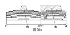
本發明的一個實施方式是一種包括電晶體的半導體裝置,電晶體包括第一絕緣膜上的第一氧化物半導體膜、第一氧化物半導體膜上的閘極絕緣膜、閘極絕緣膜上的第二氧化物半導體膜、第一氧化物半導體膜及第二氧化物半導體膜上的第二絕緣膜,第一氧化物半導體膜具有與第二氧化物半導體膜重疊的通道區域、與第二絕緣膜接觸的源極區域、以及與第二絕緣膜接觸的汲極區域,通道區域包括第一層、以及與第一層的頂面接觸並覆蓋第一層的通道寬度方向上的側面的第二層,第二氧化物半導體膜的載子密度比第一氧化物半導體膜高。One embodiment of the present invention is a semiconductor device including a transistor including a first oxide semiconductor film on a first insulating film, a gate insulating film on the first oxide semiconductor film, and a semiconductor device on the gate insulating film. A second oxide semiconductor film, a first oxide semiconductor film, and a second insulating film on the second oxide semiconductor film, the first oxide semiconductor film having a channel region overlapping the second oxide semiconductor film, and the second insulating film The source region in contact with the film and the drain region in contact with the second insulating film. The channel region includes a first layer and a second layer in contact with the top surface of the first layer and covering the side surface of the first layer in the channel width direction. Layer, the carrier of the second oxide semiconductor filmThe density is higher than that of the first oxide semiconductor film.
本發明的另一個實施方式是一種包括電晶體的半導體裝置,電晶體包括第一絕緣膜上的第一氧化物半導體膜、第一氧化物半導體膜上的閘極絕緣膜、閘極絕緣膜上的第二氧化物半導體膜、第一氧化物半導體膜及第二氧化物半導體膜上的第二絕緣膜,第一氧化物半導體膜具有與第二氧化物半導體膜重疊的通道區域、與第二絕緣膜接觸的源極區域、以及與第二絕緣膜接觸的汲極區域,通道區域包括第一層、與第一層的頂面接觸並覆蓋第一層的通道寬度方向上的側面的第二層、以及與第一層的底面接觸的第三層,第二氧化物半導體膜的載子密度比第一氧化物半導體膜高。Another embodiment of the present invention is a semiconductor device including a transistor including a first oxide semiconductor film on a first insulating film, a gate insulating film on the first oxide semiconductor film, and a gate insulating film on the gate insulating film. The second oxide semiconductor film, the first oxide semiconductor film and the second insulating film on the second oxide semiconductor film, the first oxide semiconductor film having a channel region overlapping the second oxide semiconductor film, and the second The source region in contact with the insulating film and the drain region in contact with the second insulating film. The channel region includes a first layer and a second layer in contact with the top surface of the first layer and covering the side surface of the first layer in the channel width direction. The second oxide semiconductor film has a higher carrier density than the first oxide semiconductor film, and the third layer in contact with the bottom surface of the first layer.
本發明的另一個實施方式是一種包括電晶體的半導體裝置,電晶體包括第一絕緣膜上的第一氧化物半導體膜、第一氧化物半導體膜上的閘極絕緣膜、閘極絕緣膜上的第二氧化物半導體膜、第二氧化物半導體膜上的導電膜、第一氧化物半導體膜及導電膜上的第二絕緣膜,第一氧化物半導體膜具有與第二氧化物半導體膜重疊的通道區域、與第二絕緣膜接觸的源極區域、以及與第二絕緣膜接觸的汲極區域,通道區域包括第一層、以及與第一層的頂面接觸並覆蓋第一層的通道寬度方向上的側面的第二層,第二氧化物半導體膜的載子密度比第一氧化物半導體膜高。Another embodiment of the present invention is a semiconductor device including a transistor including a first oxide semiconductor film on a first insulating film, a gate insulating film on the first oxide semiconductor film, and a gate insulating film on the gate insulating film. The second oxide semiconductor film, the conductive film on the second oxide semiconductor film, the first oxide semiconductor film, and the second insulating film on the conductive film, the first oxide semiconductor film has an overlap with the second oxide semiconductor film The channel region, the source region in contact with the second insulating film, and the drain region in contact with the second insulating film. The channel region includes a first layer and a channel in contact with the top surface of the first layer and covering the first layer In the second layer on the side surface in the width direction, the carrier density of the second oxide semiconductor film is higher than that of the first oxide semiconductor film.
本發明的另一個實施方式是一種包括電晶體的半導體裝置,電晶體包括第一絕緣膜上的第一氧化物半導體膜、第一氧化物半導體膜上的閘極絕緣膜、閘極絕緣膜上的第二氧化物半導體膜、第二氧化物半導體膜上的導電膜、第一氧化物半導體膜及導電膜上的第二絕緣膜,第一氧化物半導體膜具有與第二氧化物半導體膜重疊的通道區域、與第二絕緣膜接觸的源極區域、以及與第二絕緣膜接觸的汲極區域,通道區域包括第一層、與第一層的頂面接觸並覆蓋第一層的通道寬度方向上的側面的第二層、以及與第一層的底面接觸的第三層,第二氧化物半導體膜的載子密度比第一氧化物半導體膜高。Another embodiment of the present invention is a semiconductor device including a transistor including a first oxide semiconductor film on a first insulating film, and a gate insulating film on the first oxide semiconductor film.The edge film, the second oxide semiconductor film on the gate insulating film, the conductive film on the second oxide semiconductor film, the first oxide semiconductor film, and the second insulating film on the conductive film, the first oxide semiconductor film has A channel region overlapping the second oxide semiconductor film, a source region in contact with the second insulating film, and a drain region in contact with the second insulating film. The channel region includes the first layer and is in contact with the top surface of the first layer The second layer covering the side surface in the channel width direction of the first layer and the third layer contacting the bottom surface of the first layer. The second oxide semiconductor film has a higher carrier density than the first oxide semiconductor film.
另外,在上述方式中,閘極絕緣膜的上端部較佳為具有與第二氧化物半導體膜的下端部對齊的區域或者位於第二氧化物半導體膜的下端部的外側的區域。In addition, in the above-mentioned aspect, the upper end of the gate insulating film preferably has a region aligned with the lower end of the second oxide semiconductor film or a region located outside the lower end of the second oxide semiconductor film.
另外,在上述方式中,第二絕緣膜較佳為包含氮和氫中的一個或兩個。In addition, in the above aspect, the second insulating film preferably contains one or both of nitrogen and hydrogen.
另外,在上述方式中,電晶體較佳為還包括第二絕緣膜上的第三絕緣膜、藉由形成在第二絕緣膜及第三絕緣膜中的開口與源極區域連接的源極電極、經過形成在第二絕緣膜及第三絕緣膜中的開口與汲極區域連接的汲極電極。In addition, in the above method, the transistor preferably further includes a third insulating film on the second insulating film, and a source electrode connected to the source region through openings formed in the second insulating film and the third insulating film. A drain electrode connected to the drain region through the openings formed in the second insulating film and the third insulating film.
另外,在上述方式中,源極區域及汲極區域較佳為具有其氫濃度與第二氧化物半導體膜相同的區域。另外,在上述方式中,源極區域及汲極區域較佳為包含氫、硼、碳、氮、氟、磷、硫和稀有氣體中的一個以上。In addition, in the above-mentioned method, it is preferable that the source region and the drain region have regions with the same hydrogen concentration as the second oxide semiconductor film. In addition, in the above method, the source region and the drain region preferably contain one or more of hydrogen, boron, carbon, nitrogen, fluorine, phosphorus, sulfur, and rare gas.
另外,在上述方式中,較佳的是,第一氧化物半導體膜和第二氧化物半導體膜中的一個或兩個包含氧、In、Zn、M(M是Al、Ga、Y或Sn)。另外,在上述方式中,較佳的是,第一氧化物半導體膜和第二氧化物半導體膜中的一個或兩個具有結晶部,該結晶部具有c軸配向性。In addition, in the above-mentioned mode, it is preferable that one or both of the first oxide semiconductor film and the second oxide semiconductor film contain oxygen, In, Zn, M (M is Al, Ga, Y, or Sn) . In addition, in the above-mentioned aspect, it is preferable that one or both of the first oxide semiconductor film and the second oxide semiconductor film have a crystal portion having c-axis orientation.
本發明的另一個實施方式是一種包括根據上述各方式中的任一個的半導體裝置及顯示元件的顯示裝置。本發明的其他一個實施方式是一種包括該顯示裝置及觸控感測器的顯示模組。本發明的其他一個實施方式是一種電子裝置,包括:根據上述各方式中的任一個的半導體裝置、上述顯示裝置或上述顯示模組;以及操作鍵或電池。Another embodiment of the present invention is a display device including a semiconductor device and a display element according to any one of the above-mentioned aspects. Another embodiment of the present invention is a display module including the display device and the touch sensor. Another embodiment of the present invention is an electronic device including: the semiconductor device, the above-mentioned display device, or the above-mentioned display module according to any one of the above-mentioned modes; and an operation key or a battery.
根據本發明的一個實施方式,在包括氧化物半導體的電晶體中,藉由抑制電特性的變動可以提高可靠性。另外,根據本發明的一個實施方式,可以提供一種包括氧化物半導體的交錯型電晶體。另外,根據本發明的一個實施方式,可以提供一種包括氧化物半導體的通態電流大的電晶體。另外,根據本發明的一個實施方式,可以提供一種包括氧化物半導體的關態電流小的電晶體。另外,根據本發明的一個實施方式,可以提供一種功耗得到降低的半導體裝置。另外,根據本發明的一個實施方式,可以提供一種新穎的半導體裝置。According to one embodiment of the present invention, in a transistor including an oxide semiconductor, reliability can be improved by suppressing variation in electrical characteristics. In addition, according to an embodiment of the present invention, an interleaved transistor including an oxide semiconductor can be provided. In addition, according to an embodiment of the present invention, it is possible to provide a transistor including an oxide semiconductor with a large on-state current. In addition, according to an embodiment of the present invention, it is possible to provide a transistor including an oxide semiconductor with a small off-state current. In addition, according to an embodiment of the present invention, a semiconductor device with reduced power consumption can be provided. In addition, according to an embodiment of the present invention, a novel semiconductor device can be provided.
注意,這些效果的記載不妨礙其他效果的存在。本發明的一個實施方式並不需要具有所有上述效果。另外,這些效果以外的效果從說明書、圖式、權利要求的記載看來是顯而易見的,並可以從說明書、圖式、權利要求的記載中抽取上述目的以外的效果。Note that the description of these effects does not prevent the existence of other effects. An embodiment of the inventionThe formula does not need to have all the above effects. In addition, effects other than these effects are obvious from the description of the specification, drawings, and claims, and effects other than the above-mentioned purpose can be extracted from the description of the specification, drawings, and claims.
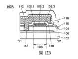
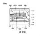
100:電晶體100: Transistor
100A:電晶體100A: Transistor
100B:電晶體100B: Transistor
100C:電晶體100C: Transistor
100D:電晶體100D: Transistor
100E:電晶體100E: Transistor
100F:電晶體100F: Transistor
100G:電晶體100G: Transistor
102:基板102: substrate
104:絕緣膜104: insulating film
106:導電膜106: conductive film
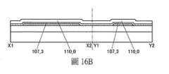
107:氧化物半導體膜107: oxide semiconductor film
107_3:氧化物半導體膜107_3: oxide semiconductor film
108:氧化物半導體膜108: oxide semiconductor film
108_1:層108_1: layer
108_2:層108_2: layer
108_3:層108_3: layer
108d:汲極區域108d: drain area
108f:區域108f: area
108i:通道區域108i: Channel area
108s:源極區域108s: source region
110:絕緣膜110: insulating film
110_0:絕緣膜110_0: insulating film
112:氧化物半導體膜112: oxide semiconductor film
112_0:氧化物半導體膜112_0: oxide semiconductor film
114:導電膜114: conductive film
116:絕緣膜116: insulating film
118:絕緣膜118: insulating film
120:導電膜120: conductive film
120a:導電膜120a: conductive film
120b:導電膜120b: conductive film
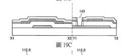
122:絕緣膜122: insulating film
140:遮罩140: Mask
141a:開口141a: opening
141b:開口141b: opening
143:開口143: opening
145:雜質元素145: impurity elements
147:空心區域147: hollow area
150:電晶體150: Transistor
160:電晶體160: Transistor
160A:電晶體160A: Transistor
160B:電晶體160B: Transistor
160C:電晶體160C: Transistor
501:像素電路501: Pixel Circuit
502:像素部502: Pixel
504:驅動電路部504: Drive Circuit Department
504a:閘極驅動器504a: Gate driver
504b:源極驅動器504b: source driver
506:保護電路506: protection circuit
507:端子部507: Terminal
550:電晶體550: Transistor
552:電晶體552: Transistor
554:電晶體554: Transistor
560:電容元件560: Capacitive element
562:電容元件562: Capacitive element
570:液晶元件570: liquid crystal element
572:發光元件572: light-emitting element
700:顯示裝置700: display device
701:基板701: substrate
702:像素部702: Pixel
704:源極驅動電路部704: Source drive circuit section
705:基板705: substrate
706:閘極驅動電路部706: Gate drive circuit section
708:FPC端子部708: FPC terminal
710:信號線710: signal line
711:佈線部711: Wiring Department
712:密封劑712: Sealant
716:FPC716: FPC
730:絕緣膜730: insulating film
732:密封膜732: Sealing Film
734:絕緣膜734: insulating film
736:彩色膜736: color film
738:遮光膜738: shading film
750:電晶體750: Transistor
752:電晶體752: Transistor
760:連接電極760: Connect electrode
770:平坦化絕緣膜770: Flattening insulating film
772:導電膜772: conductive film
774:導電膜774: conductive film
775:液晶元件775: liquid crystal element
776:液晶層776: liquid crystal layer
778:結構體778: structure
780:異方性導電膜780: Anisotropic conductive film
782:發光元件782: Light-emitting element
784:導電膜784: conductive film
786:EL層786: EL layer
788:導電膜788: conductive film
790:電容元件790: Capacitive element
1280a:p型電晶體1280a: p-type transistor
1280b:n型電晶體1280b: n-type transistor
1280c:n型電晶體1280c: n-type transistor
1281:電容元件1281: Capacitive element
1282:電晶體1282: Transistor
1311:佈線1311: Wiring
1312:佈線1312: Wiring
1313:佈線1313: Wiring
1314:佈線1314: Wiring
1315:佈線1315: Wiring
1316:佈線1316: Wiring
1317:佈線1317: Wiring
1351:電晶體1351: Transistor
1352:電晶體1352: Transistor
1353:電晶體1353: Transistor
1354:電晶體1354: Transistor
1360:光電轉換元件1360: photoelectric conversion element
1401:信號1401: signal
1402:信號1402: signal
1403:信號1403: signal
1404:信號1404: signal
1405:信號1405: signal
8000:顯示模組8000: display module
8001:上蓋8001: upper cover
8002:下蓋8002: lower cover
8003:FPC8003: FPC
8004:觸控面板8004: touch panel
8005:FPC8005: FPC
8006:顯示面板8006: display panel
8007:背光8007: Backlight
8008:光源8008: light source
8009:框架8009: frame
8010:印刷電路板8010: printed circuit board
8011:電池8011: battery
9000:外殼9000: Shell
9001:顯示部9001: Display Department
9003:揚聲器9003: Speaker
9005:操作鍵9005: Operation key
9006:連接端子9006: Connection terminal
9007:感測器9007: Sensor
9008:麥克風9008: Microphone
9050:操作按鈕9050: Operation button
9051:資訊9051: Information
9052:資訊9052: Information
9053:資訊9053: Information
9054:資訊9054: Information
9055:鉸鏈部9055: Hinge
9100:電視機9100: TV
9101:可攜式資訊終端9101: Portable Information Terminal
9102:可攜式資訊終端9102: Portable Information Terminal
9200:可攜式資訊終端9200: portable information terminal
9201:可攜式資訊終端9201: Portable Information Terminal
1111:第一佈線1111: first wiring
1112:第二佈線1112: second wiring
1113:第三佈線1113: third wiring
1114:第四佈線1114: Fourth wiring
1115:第五佈線1115: Fifth wiring
1116:第六佈線1116: sixth wiring
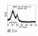
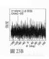
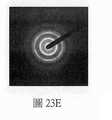
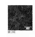
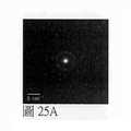
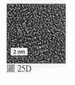
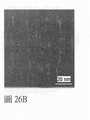
在圖式中:圖1A至圖1C是說明半導體裝置的頂面及剖面的圖;圖2A和圖2B是說明半導體裝置的剖面的圖;圖3A和圖3B是說明半導體裝置的剖面的圖;圖4A和圖4B是說明半導體裝置的剖面的圖;圖5A和圖5B是說明半導體裝置的剖面的圖;圖6A和圖6B是說明半導體裝置的剖面的圖;圖7A和圖7B是說明半導體裝置的剖面的圖;圖8A和圖8B是說明半導體裝置的剖面的圖;圖9A至圖9C是說明半導體裝置的頂面及剖面的圖;圖10A和圖10B是說明半導體裝置的剖面的圖;圖11A至圖11C是說明半導體裝置的頂面及剖面的圖;圖12A和圖12B是說明半導體裝置的剖面的圖;圖13A和圖13B是說明半導體裝置的剖面的圖;圖14A和圖14B是說明半導體裝置的剖面的圖;圖15A和圖15B是說明帶結構的圖;圖16A至圖16D是說明半導體裝置的製造方法的剖面圖;圖17A至圖17D是說明半導體裝置的製造方法的剖面圖;圖18A至圖18C是說明半導體裝置的製造方法的剖面圖;圖19A至圖19D是說明半導體裝置的製造方法的剖面圖;圖20A至圖20D是說明半導體裝置的製造方法的剖面圖;圖21A至圖21C是說明半導體裝置的製造方法的剖面圖;圖22A至圖22C是說明半導體裝置的製造方法的剖面圖;圖23A至圖23E是說明CAAC-OS及單晶氧化物半導體的利用XRD的結構分析的圖以及CAAC-OS的選區電子繞射圖案;圖24A至圖24E是CAAC-OS的剖面TEM影像、平面TEM影像及其影像分析;圖25A至圖25D是nc-OS的電子繞射圖案以及nc-OS的剖面TEM影像;圖26A和圖26B是a-like OS的剖面TEM影像;圖27示出In-Ga-Zn氧化物的電子照射所引起的結晶部的變化;圖28是示出顯示裝置的一個實施方式的俯視圖;圖29是示出顯示裝置的一個實施方式的剖面圖;圖30是示出顯示裝置的一個實施方式的剖面圖;圖31是說明半導體裝置的電路結構的圖;圖32A和圖32B分別是說明像素電路的結構的圖及說明像素電路的工作的時序圖;圖33A至圖33C是說明顯示裝置的方塊圖及電路圖;圖34是說明顯示模組的圖;圖35A至圖35G是說明電子裝置的圖。In the drawings: FIGS. 1A to 1C are diagrams illustrating the top surface and cross-section of the semiconductor device; FIGS. 2A and 2B are diagrams illustrating the cross-section of the semiconductor device; FIGS. 3A and 3B are diagrams illustrating the cross-section of the semiconductor device; FIGS. 4A and 4B are diagrams illustrating the cross-section of the semiconductor device; FIGS. 5A and 5B are diagrams illustrating the cross-section of the semiconductor device; FIGS. 6A and 6B are diagrams illustrating the cross-section of the semiconductor device; FIGS. 7A and 7B are diagrams illustrating the semiconductor device. Figures 8A and 8B are diagrams illustrating the cross-section of the semiconductor device; Figures 9A to 9C are diagrams illustrating the top surface and cross-section of the semiconductor device; Figures 10A and 10B are diagrams illustrating the cross-section of the semiconductor device 11A to 11C are diagrams illustrating the top surface and cross-section of the semiconductor device; FIGS. 12A and 12B are diagrams illustrating the cross-section of the semiconductor device; FIGS. 13A and 13B are diagrams illustrating the cross-section of the semiconductor device; FIGS. 14A and FIG. 14B is a diagram illustrating a cross-section of a semiconductor device; FIGS. 15A and 15B are diagrams illustrating a tape structure; FIGS. 16A to 16D are cross-sectional views illustrating a method of manufacturing a semiconductor device;17A to 17D are cross-sectional views illustrating a method of manufacturing a semiconductor device; FIGS. 18A to 18C are cross-sectional views illustrating a method of manufacturing a semiconductor device; FIGS. 19A to 19D are cross-sectional views illustrating a method of manufacturing a semiconductor device; FIG.
下面,參照圖式對實施方式進行說明。但是,所屬技術領域的通常知識者可以很容易地理解一個事實,就是實施方式可以以多個不同形式來實施,其方式和詳細內容可以在不脫離本發明的精神及其範圍的條件下被變換為各種各樣的形式。因此,本發明不應該被解釋為僅限定在下面的實施方式所記載的內容中。Hereinafter, embodiments will be described with reference to the drawings. However, those skilled in the art can easily understand the fact that the embodiment can be implemented in a number of different forms, and the method and details can be changed without departing from the spirit and scope of the present invention. In various forms. Therefore, the present invention should not be interpreted as being limited to the content described in the following embodiments.
注意,在圖式中,有時為了明確起見,誇大表示各組件的大小、層的厚度或區域。因此,本發明並不一定限定於該尺寸。此外,在圖式中,示意性地示出理想的例子,而不侷限於圖式所示的形狀或數值等。Note that in the drawings, sometimes for the sake of clarity, the size of each component, layer thickness or area is exaggerated. Therefore, the present invention is not necessarily limited to this size. In addition, in the drawings, ideal examples are schematically shown, and are not limited to the shapes or numerical values shown in the drawings.
另外,在本說明書中使用的“第一”、“第二”、“第三”等序數詞是為了方便識別組件而附的,而不是為了在數目方面上進行限定的。In addition, the ordinal numbers such as "first", "second", and "third" used in this specification are attached for the convenience of identifying components, and are not limited in terms of numbers.
在本說明書中,為了方便起見,使用“上”、“下”等表示配置的詞句以參照圖式說明組件的位置關係。另外,組件的位置關係根據描述各組件的方向適當地改變。因此,不侷限於在說明書中說明的詞句,根據情況可以適當地更換。In this specification, for the sake of convenience, terms such as "upper" and "lower" are used to indicate configuration to describe the positional relationship of the components with reference to the drawings. In addition, the positional relationship of the components is appropriately changed according to the direction in which each component is described. Therefore, it is not limited to the words and sentences described in the specification, and can be changed appropriately according to the situation.
在本說明書等中,電晶體是指至少包括閘極、汲極以及源極這三個端子的元件。電晶體在汲極(汲極端子、汲極區域或汲極電極)與源極(源極端子、源極區域或源極電極)之間具有通道區域,並且電流能夠流過汲極、通道區域以及源極。注意,在本說明書等中,通道區域是指電流主要流過的區域。In this specification and the like, a transistor refers to an element including at least three terminals of a gate, a drain, and a source. The transistor is in the drain (drain terminal, drain region or drain electrode) and source (sourceThere is a channel region between the terminal, the source region or the source electrode), and current can flow through the drain, the channel region and the source. Note that in this specification and the like, the channel area refers to an area through which current mainly flows.
另外,在使用極性不同的電晶體的情況或電路工作中的電流方向變化的情況等下,源極及汲極的功能有時互相調換。因此,在本說明書等中,源極和汲極可以互相調換。In addition, when transistors with different polarities are used, or when the direction of current in circuit operation changes, the functions of the source and drain may be interchanged. Therefore, in this specification and the like, the source and drain can be interchanged.
在本說明書等中,“電連接”包括藉由“具有某種電作用的元件”連接的情況。在此,“具有某種電作用的元件”只要可以進行連接目標間的電信號的授受,就對其沒有特別的限制。例如,“具有某種電作用的元件”不僅包括電極和佈線,而且還包括電晶體等的切換元件、電阻元件、電感器、電容元件、其他具有各種功能的元件等。In this specification and the like, "electrical connection" includes the case of connection by "a component having a certain electrical function". Here, the "component with a certain electrical function" is not particularly limited as long as it can transmit and receive electrical signals between connection targets. For example, "an element having a certain electrical function" includes not only electrodes and wiring, but also switching elements such as transistors, resistance elements, inductors, capacitor elements, and other elements having various functions.
在本說明書等中,“平行”是指兩條直線形成的角度為-10°以上且10°以下的狀態。因此,也包括該角度為-5°以上且5°以下的狀態。另外,“垂直”是指兩條直線形成的角度為80°以上且100°以下的狀態。因此也包括85°以上且95°以下的角度的狀態。In this specification and the like, "parallel" refers to a state where the angle formed by two straight lines is -10° or more and 10° or less. Therefore, the state where the angle is -5° or more and 5° or less is also included. In addition, "perpendicular" refers to a state where the angle formed by two straight lines is 80° or more and 100° or less. Therefore, the state of an angle of 85° or more and 95° or less is also included.
在本說明書等中,“膜”和“層”可以相互調換。例如,有時可以將“導電層”換稱為“導電膜”。或者,例如有時可以將“絕緣膜”換稱為“絕緣層”。In this specification and the like, "film" and "layer" can be interchanged. For example, the "conductive layer" may sometimes be referred to as the "conductive film". Alternatively, for example, the "insulating film" may be changed to an "insulating layer".
另外,在本說明書等中,在沒有特別的說明的情況下,關態電流是指電晶體處於關閉狀態(也稱為非導通狀態、遮斷狀態)時的汲極電流。在沒有特別的說明的情況下,在n通道型電晶體中,關閉狀態是指閘極與源極間的電壓Vgs低於臨界電壓Vth的狀態,在p通道型電晶體中,關閉狀態是指閘極與源極間的電壓Vgs高於臨界電壓Vth的狀態。例如,n通道型電晶體的關態電流有時是指閘極與源極間的電壓Vgs低於臨界電壓Vth時的汲極電流。In addition, in this specification and the like, unless otherwise specified, the off-state current refers to the drain current when the transistor is in the off state (also referred to as the non-conducting state or the blocking state). Unless otherwise specified, in an n-channel transistor, the off state refers to a state where the voltage Vgs between the gate and source is lower than the threshold voltage Vth, and in a p-channel transistor, the off state refers to A state where the voltage Vgs between the gate and the source is higher than the threshold voltage Vth. For example, the off-state current of an n-channel transistor sometimes refers to the drain current when the voltage Vgs between the gate and the source is lower than the threshold voltage Vth.
電晶體的關態電流有時取決於Vgs。因此,“電晶體的關態電流為I以下”有時指存在使電晶體的關態電流成為I以下的Vgs的值。電晶體的關態電流有時是指預定的Vgs中的關閉狀態、預定的範圍內的Vgs中的關閉狀態或能夠獲得充分被降低的關態電流的Vgs中的關閉狀態等時的關態電流。The off-state current of the transistor sometimes depends on Vgs. Therefore, "the off-state current of the transistor is I or less" sometimes means that there is a value of Vgs that makes the off-state current of the transistor be I or less. The off-state current of the transistor sometimes refers to the off-state in a predetermined Vgs, the off-state in Vgs within a predetermined range, or the off-state in Vgs that can obtain a sufficiently reduced off-state current. .
作為一個例子,設想一種n通道型電晶體,該n通道型電晶體的臨界電壓Vth為0.5V,Vgs為0.5V時的汲極電流為1×10⁻⁹A,Vgs為0.1V時的汲極電流為1×10-13A,Vgs為-0.5V時的汲極電流為1×10-19A,Vgs為-0.8V時的汲極電流為1×10-22A。在Vgs為-0.5V時或在Vgs為-0.5V至-0.8V的範圍內,該電晶體的汲極電流為1×10-19A以下,所以有時稱該電晶體的關態電流為1×10-19A以下。由於存在該電晶體的汲極電流為1×10-22A以下的Vgs,因此有時稱該電晶體的關態電流為1×10-22A以下。As an example, imagine an n-channel type transistor, the threshold voltage Vth of the n-channel type transistor is 0.5V, the drain current when Vgs is 0.5V is 1×10⁻⁹ A, and the drain current when Vgs is 0.1V The pole current is 1×10-13 A, the drain current when Vgs is -0.5V is 1×10-19 A, and when Vgs is -0.8V, the drain current is 1×10-22 A. When Vgs is -0.5V or in the range of -0.5V to -0.8V, the drain current of the transistor is 1×10-19 A or less, so the off-state current of the transistor is sometimes called 1×10-19 A or less. Since the drain current of the transistor is Vgs below 1×10-22 A, it is sometimes called the off-state current of the transistor below 1×10-22 A.
在本說明書等中,有時以每通道寬度W的電流值表示具有通道寬度W的電晶體的關態電流。另外,有時以每預定的通道寬度(例如1μm)的電流值表示具有通道寬度W的電晶體的關態電流。在為後者時,關態電流的單位有時以具有電流/長度的因次的單位(例如,A/μm)表示。In this specification and the like, the off-state current of a transistor having a channel width W is sometimes expressed as a current value per channel width W. In addition, the off-state current of a transistor having a channel width W may be expressed by a current value per predetermined channel width (for example, 1 μm). In the latter case, the unit of off-state current is sometimes expressed in a unit having a current/length dimension (for example, A/μm).
電晶體的關態電流有時取決於溫度。在本說明書中,在沒有特別的說明的情況下,關態電流有時表示室溫、60℃、85℃、95℃或125℃下的關態電流。或者,有時表示保證包括該電晶體的半導體裝置等的可靠性的溫度或者包括該電晶體的半導體裝置等被使用的溫度(例如,5℃至35℃中的任一溫度)下的關態電流。“電晶體的關態電流為I以下”是指:在室溫、60℃、85℃、95℃、125℃、保證包括該電晶體的半導體裝置等的可靠性的溫度或者包括該電晶體的半導體裝置等被使用的溫度(例如,5℃至35℃中的任一溫度)下,存在使電晶體的關態電流成為I以下的Vgs的值。The off-state current of a transistor sometimes depends on temperature. In this specification, unless otherwise specified, the off-state current sometimes means the off-state current at room temperature, 60°C, 85°C, 95°C, or 125°C. Or, sometimes it indicates the off state at a temperature that guarantees the reliability of the semiconductor device including the transistor or the like or the temperature at which the semiconductor device including the transistor is used (for example, any temperature from 5°C to 35°C) Current. "The off-state current of the transistor is below I" means: at room temperature, 60°C, 85°C, 95°C, 125°C, a temperature that guarantees the reliability of a semiconductor device including the transistor, or a temperature that includes the transistor At a temperature at which a semiconductor device or the like is used (for example, any temperature from 5°C to 35°C), there is a value of Vgs such that the off-state current of the transistor becomes I or less.
電晶體的關態電流有時取決於汲極與源極間的電壓Vds。在本說明書中,在沒有特別的說明的情況下,關態電流有時表示Vds為0.1V、0.8V、1V、1.2V、1.8V、2.5V、3V、3.3V、10V、12V、16V或20V時的關態電流。或者,有時表示保證包括該電晶體的半導體裝置等的可靠性的Vds,或者,有時表示包括該電晶體的半導體裝置等所使用的Vds下的關態電流。“電晶體的關態電流為I以下”是指:在Vds為0.1V、0.8V、1V、1.2V、1.8V、2.5V、3V、3.3V、10V、12V、16V、20V、在保證包括該電晶體的半導體裝置等的可靠性的Vds或包括該電晶體的半導體裝置等所使用的Vds下,存在使電晶體的關態電流成為I以下的Vgs的值。The off-state current of the transistor sometimes depends on the voltage Vds between the drain and the source. In this specification, unless otherwise specified, the off-state current sometimes means that Vds is 0.1V, 0.8V, 1V, 1.2V, 1.8V, 2.5V, 3V, 3.3V, 10V, 12V, 16V or Off-state current at 20V. Alternatively, it may indicate Vds that guarantees the reliability of a semiconductor device or the like including the transistor, or it may indicate an off-state current at Vds used in a semiconductor device or the like including the transistor. "The off-state current of the transistor is below I" means: when Vds is 0.1V, 0.8V, 1V, 1.2V, 1.8V, 2.5V, 3V, 3.3V, 10V, 12V, 16V, 20V, the guarantee includes Vds of the reliability of the semiconductor device of the transistor or used in the semiconductor device including the transistorAt Vds, there is a value of Vgs at which the off-state current of the transistor becomes I or less.
在上述關態電流的說明中,可以將汲極換稱為源極。也就是說,關態電流有時指電晶體處於關閉狀態時流過源極的電流。In the above description of the off-state current, the drain can be referred to as the source. In other words, the off-state current sometimes refers to the current flowing through the source when the transistor is off.
在本說明書等中,有時將關態電流記作洩漏電流。在本說明書等中,關態電流例如有時指當電晶體處於關閉狀態時流在源極與汲極間的電流。In this manual, etc., off-state current is sometimes referred to as leakage current. In this specification and the like, the off-state current sometimes refers to the current flowing between the source and the drain when the transistor is in the off state.
在本說明書等中,半導體的雜質是指構成半導體的主要成分之外的物質。例如,濃度低於0.1atomic%的元素是雜質。當包含雜質時,有可能在半導體中形成DOS(Density of States:態密度),載子移動率有可能降低或結晶性有可能降低。在半導體包含氧化物半導體時,作為改變半導體特性的雜質,例如有第1族元素、第2族元素、第14族元素、第15族元素或主要成分之外的過渡金屬等,尤其是,有氫(包含於水中)、鋰、鈉、矽、硼、磷、碳、氮等。在是氧化物半導體的情況下,有時例如由於氫等雜質的混入導致氧缺陷的產生。此外,當半導體包含矽時,作為改變半導體特性的雜質,例如有氧、除氫之外的第1族元素、第2族元素、第13族元素、第15族元素等。In this specification and the like, semiconductor impurities refer to substances other than the main components constituting the semiconductor. For example, elements with a concentration lower than 0.1 atomic% are impurities. When impurities are included, DOS (Density of States) may be formed in the semiconductor, and the carrier mobility may decrease or the crystallinity may decrease. When the semiconductor includes an oxide semiconductor, as impurities that change the characteristics of the semiconductor, there are, for example,
實施方式1
在本實施方式中,使用圖1A至圖22C說明包括電晶體的半導體裝置、以及該半導體裝置的製造方法的例子。In this embodiment mode, a semiconductor device including a transistor,And an example of the manufacturing method of the semiconductor device.
〈1-1. 半導體裝置的結構例子1〉〈1-1. Structure example 1 of semiconductor device〉
圖1A至圖1C示出包括電晶體的半導體裝置的一個例子。圖1A至圖1C所示的電晶體具有頂閘極結構。1A to 1C show an example of a semiconductor device including a transistor. The transistors shown in FIGS. 1A to 1C have a top gate structure.
圖1A是電晶體100的俯視圖,圖1B是沿著圖1A的點劃線X1-X2的剖面圖,圖1C是沿著圖1A的點劃線Y1-Y2的剖面圖。注意,為了明確起見,在圖1A中,省略絕緣膜110等組件。注意,有時在後面的電晶體的俯視圖中,與圖1A同樣地省略組件的一部分。此外,有時將點劃線X1-X2方向稱為通道長度(L)方向,將點劃線Y1-Y2方向稱為通道寬度(W)方向。1A is a top view of the
圖1A至圖1C所示的電晶體100包括形成在基板102上的絕緣膜104、絕緣膜104上的氧化物半導體膜108、氧化物半導體膜108上的絕緣膜110、絕緣膜110上的氧化物半導體膜112、以及絕緣膜104、氧化物半導體膜108及氧化物半導體膜112上的絕緣膜116。氧化物半導體膜108具有與氧化物半導體膜112重疊的通道區域108i、與絕緣膜116接觸的源極區域108s、以及與絕緣膜116接觸的汲極區域108d,通道區域108i包括層108_2、與層108_2的頂面接觸並覆蓋層108_2的通道寬度方向上的側面的層108_3。The
電晶體100也可以包括絕緣膜116上的絕緣膜118、經過形成在絕緣膜116、118中的開口141a與源極區域108s電連接的導電膜120a、以及經過形成在絕緣膜116、118中的開口141b與汲極區域108d電連接的導電膜120b。The
在本說明書等中,有時將絕緣膜104、絕緣膜116及絕緣膜118分別稱為第一絕緣膜、第二絕緣膜及第三絕緣膜。絕緣膜110被用作閘極絕緣膜,氧化物半導體膜112被用作閘極電極。導電膜120a被用作源極電極,導電膜120b被用作汲極電極。In this specification and the like, the insulating
在通道區域108i的通道寬度(W)方向上的側面或其附近,由於加工時的損傷而容易形成缺陷(例如是氧缺陷)或者容易發生雜質的附著所導致的污染。因此,即使通道區域108i是實質上本質的,也由於被施加電場等應力而通道區域108i的通道寬度(W)方向上的側面或其附近活化,因此容易成為低電阻(n型)區域。當通道區域108i的通道寬度(W)方向上的側面或其附近是n型區域時,有時該n型區域被用作載子的路徑而形成寄生通道。On or near the side surface of the
於是,在本發明的一個實施方式的半導體裝置中,通道區域108i具有疊層結構,疊層中的一個層的通道寬度(W)方向上的側面被另一個層覆蓋。藉由採用該結構,可以減少通道區域108i的側面或其附近的缺陷或雜質附著。Therefore, in the semiconductor device of one embodiment of the present invention, the
注意,在圖1B和圖1C中,通道區域108i具有層108_2和層108_3這兩層的疊層結構,但是不侷限於此。例如,也可以採用圖2A和圖2B所示的疊層結構。Note that in FIGS. 1B and 1C, the
圖2A和圖2B是電晶體100A的剖面圖。電晶體100A的俯視圖與圖1A所示的電晶體100相同,因此援用圖1A進行說明。圖2A是沿著圖1A的點劃線X1-X2的剖面圖,圖2B是沿著圖1A的點劃線Y1-Y2的剖面圖。2A and 2B are cross-sectional views of the
電晶體100A所包括的氧化物半導體膜108具有與氧化物半導體膜112重疊的通道區域108i、與絕緣膜116接觸的源極區域108s、與絕緣膜116接觸的汲極區域108d。通道區域108i包括層108_2、與層108_2的頂面接觸並覆蓋層108_2的通道寬度方向上的側面的層108_3、以及與層108_2的底面接觸的層108_1。The
如此,電晶體100A的與上述電晶體100之間的不同之處在於氧化物半導體膜108的結構。電晶體100A的其他結構與電晶體100相同,並發揮相同的效果。As such, the difference between the
氧化物半導體膜108中的層108_1、層108_2、層108_3包含至少一個相同的元素。因此,在層108_1和層108_2之間的介面或層108_2和層108_3之間的介面不容易發生介面散射。由此,在該介面處載子的移動不被阻礙,因此電晶體100及電晶體100A的場效移動率(有時,簡單地稱為移動率或μFE)得到提高。The layer 108_1, the layer 108_2, and the layer 108_3 in the
層108_1、層108_2和層108_3都包含金屬氧化物,該金屬氧化物較佳為至少包含銦(In)或鋅(Zn)。The layer 108_1, the layer 108_2 and the layer 108_3 all contain a metal oxide, and the metal oxide preferably contains at least indium (In) or zinc (Zn).
當氧化物半導體膜包含In時,例如其載子移動率(電子移動率)得到提高。當氧化物半導體膜包含Zn時,氧化物半導體膜容易晶化。When the oxide semiconductor film contains In, for example, its carrier mobility (electron mobility) is improved. When the oxide semiconductor film contains Zn, the oxide semiconductor film is easily crystallized.
當氧化物半導體膜包含被用作穩定劑的元素M時,例如氧化物半導體膜的能隙(Eg)變寬。適合於本發明的一個實施方式的氧化物半導體膜的能隙為2eV以上,較佳為2.5eV以上,更佳為3eV以上。如此,藉由將能隙較寬的金屬氧化物用於氧化物半導體膜108,可以降低電晶體100、電晶體100A的關態電流。元素M是與氧的鍵能高的元素,元素M與氧的鍵能比In與氧的鍵能高。When the oxide semiconductor film contains the element M used as a stabilizer, for example, the energy gap (Eg) of the oxide semiconductor film becomes wider. The energy gap of the oxide semiconductor film suitable for one embodiment of the present invention is 2 eV or more, preferably 2.5 eV or more, and more preferably 3 eV or more. In this way, by using a metal oxide with a wide energy gap for the
另外,作為適合於本發明的一個實施方式的半導體裝置的氧化物半導體膜,典型地可以使用In-Zn氧化物、In-M氧化物、In-M-Zn氧化物。其中,較佳為使用In-M-Zn氧化物(M為鋁(Al)、鎵(Ga)、釔(Y)或錫(Sn))。尤其是,較佳為使用以M為Ga的In-Ga-Zn氧化物(以下,有時稱為IGZO)。In addition, as an oxide semiconductor film suitable for the semiconductor device of one embodiment of the present invention, In-Zn oxide, In-M oxide, and In-M-Zn oxide can be typically used. Among them, In-M-Zn oxide (M is aluminum (Al), gallium (Ga), yttrium (Y), or tin (Sn)) is preferably used. In particular, it is preferable to use an In-Ga-Zn oxide in which M is Ga (hereinafter, sometimes referred to as IGZO).
在層108_2包含In-M-Zn氧化物時,除了Zn及氧之外的In與M的比例較佳為:In的比率大於25atomic%且M的比率低於75atomic%,更佳為In的比率大於34atomic%且M的比率低於66atomic%。尤其是,層108_2較佳為具有In的原子個數比為M的原子個數比以上的區域。When the layer 108_2 contains In-M-Zn oxide, the ratio of In to M other than Zn and oxygen is preferably: the ratio of In is greater than 25 atomic% and the ratio of M is less than 75 atomic%, more preferably the ratio of In It is greater than 34atomic% and the ratio of M is lower than 66atomic%. Especially, layer 108_2 is betterIt is a region in which the ratio of the number of atoms of In is greater than the ratio of the number of atoms of M.
當層108_2具有In的原子個數比為M的原子個數比以上的區域時,電晶體的場效移動率可以得到提高。明確而言,電晶體100、電晶體100A的場效移動率可以大於10cm2/Vs,較佳為大於30cm2/Vs。When the layer 108_2 has a region where the atomic ratio of In is greater than the atomic ratio of M, the field effect mobility of the transistor can be improved. Specifically, the field effect mobility of the
例如,場效移動率高的電晶體可以縮減其通道寬度。因此,藉由將該電晶體用於生成閘極信號的掃描線驅動電路(也稱為閘極驅動器)或與掃描線驅動電路所包括的移位暫存器的輸出端子連接的解多工器,可以縮小掃描線驅動電路的尺寸,而可以提供一種邊框寬度小(也稱為窄邊框)的半導體裝置或顯示裝置。或者,可以降低閘極電壓,因此可以降低顯示裝置的功耗。For example, a transistor with high field effect mobility can reduce its channel width. Therefore, by using the transistor for a scan line driver circuit (also called a gate driver) that generates a gate signal or a demultiplexer connected to the output terminal of a shift register included in the scan line driver circuit Therefore, the size of the scan line driving circuit can be reduced, and a semiconductor device or display device with a small frame width (also called a narrow frame) can be provided. Alternatively, the gate voltage can be reduced, so the power consumption of the display device can be reduced.
另外,藉由提高電晶體的場效移動率,可以實現一種清晰度高的顯示裝置。可以將該電晶體適當地用作例如以4K×2K(水平方向的像素數為3840,垂直方向的像素數為2160)或8K×4K(水平方向的像素數為7680,垂直方向的像素數為4320)為代表的清晰度高的顯示裝置的像素電路或驅動電路的電晶體。In addition, by increasing the field effect mobility of the transistor, a high-definition display device can be realized. This transistor can be suitably used as 4K×2K (the number of pixels in the horizontal direction is 3840, the number of pixels in the vertical direction is 2160) or 8K×4K (the number of pixels in the horizontal direction is 7680, and the number of pixels in the vertical direction is 4320) represents a transistor of a pixel circuit or a driving circuit of a high-resolution display device.
另一方面,當層108_2具有In的原子個數比為M的原子個數比以上的區域時,能隙(Eg)變窄,因此在光照射時電晶體的電特性容易發生變動。但是在本發明的一個實施方式的半導體裝置中,在層108_2上形成有層108_3。或者,在層108_1上形成有層108_2。On the other hand, when the layer 108_2 has a region where the number of atoms of In is greater than the number of atoms of M, the energy gap (Eg) is narrowed, and therefore, the electrical characteristics of the transistor are likely to change during light irradiation. However, in the semiconductor device of one embodiment of the present invention, a layer 108_2 is formed108_3. Alternatively, a layer 108_2 is formed on the layer 108_1.
層108_1及層108_3具有其In的原子個數比小於層108_2的區域。因此,層108_1及層108_3的Eg比層108_2寬。因此,藉由層疊層108_2和層108_3或層疊層108_1、層108_2和層108_3,可以提高電晶體的對光負偏壓應力測試的耐性。The layer 108_1 and the layer 108_3 have regions where the ratio of the number of In atoms is smaller than that of the layer 108_2. Therefore, Eg of layer 108_1 and layer 108_3 is wider than layer 108_2. Therefore, by laminating the layer 108_2 and the layer 108_3 or the layer 108_1, the layer 108_2 and the layer 108_3, the resistance of the transistor to the light negative bias stress test can be improved.
在層108_1及層108_3包含In-M-Zn氧化物時,除了Zn及氧之外的In與M的比例較佳為:In的比率小於75atomic%且M的比率大於25atomic%,更佳為In的比率小於66atomic%且M的比率大於34atomic%。尤其是,層108_1及層108_3較佳為具有M的原子個數比為In的原子個數比以上的區域。When the layer 108_1 and the layer 108_3 contain In-M-Zn oxide, the ratio of In to M other than Zn and oxygen is preferably: the ratio of In is less than 75 atomic% and the ratio of M is greater than 25 atomic%, more preferably In The ratio of is less than 66atomic% and the ratio of M is greater than 34atomic%. In particular, it is preferable that the layer 108_1 and the layer 108_3 have a region in which the atomic number ratio of M is greater than the atomic number ratio of In.
當層108_1及層108_3以In以上的原子個數比包含元素M時,有時有如下效果:(1)能隙變寬(2)電子親和力變小(3)遮蔽來自外部的雜質(4)絕緣性變高。此外,由於元素M是與氧的鍵合力強的金屬元素,所以藉由包含其原子個數比為In以上的M,不容易產生氧缺陷。When the layer 108_1 and the layer 108_3 contain the element M with an atomic ratio greater than In, the following effects are sometimes obtained: (1) The energy gap becomes wider (2) The electron affinity becomes smaller (3) The external impurities are shielded (4) The insulation becomes higher. In addition, since the element M is a metal element with a strong bonding force to oxygen, by including M whose atomic ratio is In or more, oxygen defects are less likely to occur.
層108_1及層108_3所包含的元素M的原子個數較佳為層108_2所包含的元素M的原子個數以上。典型的是,層108_1及層108_3所包含的元素M的原子個數較佳為層108_2所包含的元素M的原子個數的1.5倍以上,更佳為2倍以上。The number of atoms of the element M contained in the layer 108_1 and the layer 108_3 is preferably more than the number of atoms of the element M contained in the layer 108_2. Typically, the number of atoms of the element M contained in the layer 108_1 and the layer 108_3 is preferably at least 1.5 times the number of atoms of the element M contained in the layer 108_2, and more preferably at least twice.
層108_2所包含的In的原子個數較佳為層108_1及層108_3所包含的In的原子個數以上。典型的是,層108_2所包含的In的原子個數較佳為層108_1及層108_3所包含的In的原子個數的1.5倍以上,更佳為2倍以上。此時,層108_2被用作電晶體100、電晶體100A中的通道區域。由於該結構,而可以期待如下效果:電晶體100、電晶體100A的通態電流增大且場效移動率得到提高。場效移動率高的電晶體有時具有負臨界電壓的電特性(也稱為常導通特性)。這是因為如下緣故:因該電晶體所包括的氧化物半導體膜中的氧缺陷而產生電荷,導致低電阻化。當電晶體具有常導通特性時,產生各種問題,諸如在工作時容易產生工作故障或者在非工作時功耗增大等。因此,層108_2較佳為後述的雜質或缺陷(氧缺陷等)少的CAAC-OS。The number of In atoms included in the layer 108_2 is preferably more than the number of In atoms included in the layer 108_1 and the layer 108_3. Typically, the number of In atoms contained in the layer 108_2 is preferably at least 1.5 times the number of In atoms contained in the layer 108_1 and the layer 108_3, and more preferably at least twice. At this time, the layer 108_2 is used as a channel region in the
〈1-2. 帶結構〉〈1-2. With structure〉
接著,使用圖15A和圖15B說明圖1A至圖1C所示的電晶體100、圖2A和圖2B所示的電晶體100A的每一個中的氧化物半導體膜及與該氧化物半導體膜接觸的絕緣膜的帶結構。Next, the oxide semiconductor film in each of the
圖15A示出絕緣膜104、層108_2、層108_3及絕緣膜110的厚度方向上的帶結構,圖15B示出絕緣膜104、層108_1、層108_2、層108_3及絕緣膜110的厚度方向上的帶結構。在帶結構中,為了容易理解,示出絕緣膜104、層108_1、108_2、108_3及絕緣膜110的導帶底能階(Ec)。15A shows the tape structure in the thickness direction of the insulating
另外,在此,作為絕緣膜104及絕緣膜110使用氧化矽膜,作為層108_1利用使用其金屬元素的原子個數比為In:Ga:Zn=1:1:1.2的金屬氧化物靶材形成的氧化物半導體膜,作為層108_2利用使用其金屬元素的原子個數比為In:Ga:Zn=4:2:4.1的金屬氧化物靶材形成的氧化物半導體膜,作為層108_3利用使用其金屬元素的原子個數比為In:Ga:Zn=1:1:1.2的金屬氧化物靶材形成的氧化物半導體膜。Here, a silicon oxide film is used as the insulating
如圖15A和圖15B所示,在層108_1、層108_2及層108_3中導帶底能階之間沒有能障而平緩地變化。可以說連續地變化或連續接合。因此,可以將這種能帶稱為埋入通道結構。As shown in FIG. 15A and FIG. 15B, there is no energy barrier between the bottom energy levels of the conduction band in the layer 108_1, the layer 108_2, and the layer 108_3, and the change is gentle. It can be said to continuously change or continuously join. Therefore, this energy band can be called a buried channel structure.
這是因為:層108_1、層108_2和層108_3包含共同元素,氧移動在層108_1、層108_2、層108_3之間,因此形成混合層。為了具有這種帶結構,採用如下疊層結構,其中在層108_1和層108_2之間的介面或層108_2和層108_3之間的介面沒有存在形成俘獲中心或再結合中心等缺陷能階的雜質。This is because the layers 108_1, 108_2, and 108_3 contain common elements, and oxygen moves between the layers 108_1, 108_2, and 108_3, thus forming a mixed layer. In order to have such a band structure, the following laminated structure is adopted, in which the interface between the layer 108_1 and the layer 108_2 or the interface between the layer 108_2 and the layer 108_3 does not have impurities that form defect energy levels such as trap centers or recombination centers.
如果沒有形成連接結合而在層108_1和層108_2之間的介面或層108_2和層108_3之間的介面存在雜質,則能帶失去連續性,因此載子在介面被俘獲或者再結合而消失。If no connection is formed and impurities exist in the interface between the layer 108_1 and the layer 108_2 or the interface between the layer 108_2 and the layer 108_3, the energy band loses continuity, and therefore the carriers are trapped or recombined at the interface and disappear.
為了形成連續接合,較佳為使用具備負載鎖定室的多室方式的成膜裝置(濺射裝置)在不使各膜暴露於大氣的情況下連續地層疊。在濺射裝置中的各處理室中,為了儘可能地去除成為氧化物半導體膜的雜質的水等,較佳為使用如低溫泵的吸附式的真空排氣泵進行高真空(5×10⁻⁷Pa至1×10⁻⁴Pa左右)排氣。或者,較佳為組合渦輪分子泵和冷阱來防止氣體,尤其是包含碳或氫的氣體從排氣系統倒流到處理室內。In order to form continuous bonding, it is preferable to use a multi-chamber film forming apparatus (sputtering apparatus) equipped with a load lock chamber to continuously laminate the films without exposing the films to the atmosphere. In each processing chamber of a sputtering apparatus in order to remove impurities in the water to become an oxide semiconductor film and the like as much as possible, preferably for use as vacuum pump suction type cryopump high vacuum (5 × 10- 7 Pa to 1×10⁻⁴ Pa) exhaust. Alternatively, it is preferable to combine a turbo molecular pump and a cold trap to prevent gas, especially gas containing carbon or hydrogen, from flowing back into the processing chamber from the exhaust system.
可知:藉由採用圖15A和圖15B所示的結構,層108_2成為井(well),在包括層108_2及層108_3的電晶體100中、以及包括層108_1、層108_2及層108_3的電晶體100A中,通道區域形成在層108_2中。It can be seen that by adopting the structure shown in FIGS. 15A and 15B, the layer 108_2 becomes a well, in the
在電晶體100中,即使在層108_3和絕緣膜110之間的介面附近形成起因於雜質或缺陷的陷阱能階,藉由形成層108_3也可以使層108_2遠離形成陷阱能階的區域。在電晶體100A中,即使在層108_1和絕緣膜104之間的介面附近或層108_3和絕緣膜110之間的介面附近形成起因於雜質或缺陷的陷阱能階,藉由形成層108_1及層108_3也可以使層108_2遠離形成陷阱能階的區域。In the
但是,當陷阱能階的能階低於被用作通道區域的層108_2的導帶底能階(Ec)時,電子容易被陷阱能階俘獲。在電子被陷阱能階俘獲並積蓄在陷阱能階時,在絕緣膜表面產生固定負電荷,導致電晶體的臨界電壓漂移到正方向。因此,較佳為採用陷阱能階的能階高於層108_2的導帶底能階(Ec)的結構。藉由採用這樣的結構,電子不容易積蓄在陷阱能階,而可以增高電晶體的通態電流並且可以提高場效移動率。另外,電晶體的臨界電壓變動得到降低,而電晶體具有穩定的電特性,所以是較佳的。However, when the trap energy level is lower than the conduction band bottom energy level (Ec) of the layer 108_2 used as the channel region, electrons are easily trapped by the trap energy level. When electrons are captured by the trap level and accumulated in the trap level, a fixed negative charge is generated on the surface of the insulating film, which causes the threshold voltage of the transistor to shift to the positive direction. Therefore, it is preferable to adopt a structure in which the energy level of the trap energy level is higher than the bottom energy level (Ec) of the conduction band of the layer 108_2. By adopting such a structure, electrons are not easily accumulated in the trap energy level, and the on-state current of the transistor can be increased and the field effect mobility can be improved. In addition, the critical voltage of the transistor changesThe dynamics are reduced, and the transistor has stable electrical characteristics, so it is preferable.
為了防止層108_1及層108_3被用作通道區域的一部分,層108_1及層108_3的材料的導電率較佳為低於層108_2的材料。因此,根據其物性及/或功能可以將層108_1及層108_3稱為氧化物絕緣膜。層108_1及層108_3較佳為使用其電子親和力(真空能階與導帶底能階之差)低於層108_2且其導帶底能階與層108_2的導帶底能階有差異(能帶偏移)的材料。此外,為了抑制產生起因於汲極電壓的臨界電壓之間的差異,層108_1及層108_3較佳為使用其導帶底能階比層108_2的導帶底能階更接近於真空能階的材料。例如,層108_2的導帶底能階與層108_1及層108_3的導帶底能階之差較佳為0.2eV以上,更佳為0.5eV以上。In order to prevent the layer 108_1 and the layer 108_3 from being used as a part of the channel region, the conductivity of the material of the layer 108_1 and the layer 108_3 is preferably lower than that of the layer 108_2. Therefore, the layer 108_1 and the layer 108_3 can be referred to as oxide insulating films according to their physical properties and/or functions. Layer 108_1 and layer 108_3 are better to use their electron affinity (the difference between the vacuum energy level and the bottom energy level of the conduction band) is lower than that of the layer 108_2 and the conduction band bottom energy level is different from that of the layer 108_2 (energy band Offset) material. In addition, in order to suppress the difference between the threshold voltage caused by the drain voltage, the layer 108_1 and the layer 108_3 are preferably made of materials whose conduction band bottom energy level is closer to the vacuum energy level than the conduction band bottom energy level of the layer 108_2 . For example, the difference between the bottom energy level of the conduction band of the layer 108_2 and the bottom energy levels of the conduction band of the layer 108_1 and the layer 108_3 is preferably 0.2 eV or more, more preferably 0.5 eV or more.
藉由採用這種結構,在通道區域108i中層108_2成為主要電流路徑。就是說,層108_2被用作通道區域,層108_1及層108_3被用作氧化物絕緣膜。層108_1及層108_3是包含構成形成通道區域的層108_2的金屬元素中的一種以上的氧化物半導體膜,因此,在層108_1和層108_2之間的介面或層108_2和層108_3之間的介面不容易發生介面散射。由此,在該介面處載子的移動不被阻礙,因此電晶體的場效移動率得到提高。By adopting this structure, the layer 108_2 becomes the main current path in the
〈1-3. 被用作閘極電極的氧化物半導體膜〉<1-3. Oxide semiconductor film used as gate electrode>
接著,說明被用作閘極電極的氧化物半導體膜。被用作閘極電極的氧化物半導體膜112具有對絕緣膜110供應氧的功能。當氧化物半導體膜112具有對絕緣膜110供應氧的功能時,可以使絕緣膜110包含過量氧。當絕緣膜110具有過量氧區域時,可以對氧化物半導體膜108,明確而言,對通道區域108i供應該過量氧。因此,過量氧填補通道區域108i中的氧缺陷,可以實現一種可靠性高的半導體裝置。Next, an oxide semiconductor film used as a gate electrode will be described. The
另外,為了對氧化物半導體膜108供應過量氧,形成在氧化物半導體膜108下的絕緣膜104也可以包含過量氧。但是,在絕緣膜104包含過量氧時,包含在絕緣膜104中的氧有可能也供應到氧化物半導體膜108所具有的源極區域108s及汲極區域108d。當源極區域108s及汲極區域108d被供應過量氧時,有時源極區域108s及汲極區域108d的電阻變高。In addition, in order to supply excess oxygen to the
另一方面,當形成在氧化物半導體膜108上的絕緣膜110包含過量氧時,可以只對通道區域108i選擇性地供應過量氧。或者,可以在對通道區域108i、源極區域108s及汲極區域108d供應過量氧之後,選擇性地提高源極區域108s及汲極區域108d的載子密度。On the other hand, when the insulating
絕緣膜116包含氮和氫中的一個或兩個。藉由採用絕緣膜116包含氮和氫中的一個或兩個的結構,可以對氧化物半導體膜108及氧化物半導體膜112供應氮和氫中的一個或兩個。The insulating
氧化物半導體膜112在對絕緣膜110供應氧之後從絕緣膜116被供應氮和氫中的一個或兩個,因此其載子密度得到提高。換言之,氧化物半導體膜112還被用作氧化物導電體(OC:Oxide Conductor)。因此,氧化物半導體膜112具有高於氧化物半導體膜108的載子密度並被用作閘極電極。The
氧化物半導體膜108所包括的源極區域108s、汲極區域108d以及氧化物半導體膜112可以都包含形成氧缺陷的元素。作為上述形成氧缺陷的元素,典型地可以舉出氫、硼、碳、氮、氟、磷、硫、氯、稀有氣體元素等。作為稀有氣體元素的典型例子,有氦、氖、氬、氪以及氙等。The
當對氧化物半導體膜添加雜質元素時,氧化物半導體膜中的金屬元素和氧的鍵合斷開,而形成氧缺陷。或者,當對氧化物半導體膜添加雜質元素時,與氧化物半導體膜中的金屬元素鍵合的氧與該雜質元素鍵合,氧從金屬元素脫離,而形成氧缺陷。其結果是,在氧化物半導體膜中載子密度增高且導電率得到提高。When an impurity element is added to the oxide semiconductor film, the bond between the metal element and oxygen in the oxide semiconductor film is broken, and oxygen defects are formed. Alternatively, when an impurity element is added to the oxide semiconductor film, oxygen bonded to the metal element in the oxide semiconductor film is bonded to the impurity element, and the oxygen is detached from the metal element to form an oxygen defect. As a result, the carrier density in the oxide semiconductor film is increased and the conductivity is improved.
電晶體100、電晶體100A較佳為具有絕緣膜110的側端部和氧化物半導體膜112的側端部對齊的區域。換言之,在電晶體100中,絕緣膜110的上端部和氧化物半導體膜112的下端部大致對齊。例如,藉由將氧化物半導體膜112用作遮罩對絕緣膜110進行加工,可以實現上述結構。The
如上所述,在本發明的一個實施方式的半導體裝置中,使用被用作閘極電極的氧化物半導體膜,使覆蓋被用作通道區域的氧化物半導體膜的側面並形成在通道區域上的絕緣膜包含過量氧。藉由採用這種結構,可以提供一種可靠性高的半導體裝置。As described above, in the semiconductor device of one embodiment of the present invention, the oxide semiconductor film used as the gate electrode is used, so that the side surface of the oxide semiconductor film used as the channel region is covered and formed on the channel region. The insulating film contains excessive oxygen. By adopting this structure,Provide a highly reliable semiconductor device.
接著,詳細地說明圖1A至圖1C所示的半導體裝置的組件。Next, the components of the semiconductor device shown in FIGS. 1A to 1C will be described in detail.
〈1-4. 半導體裝置的組件〉<1-4. Components of semiconductor devices>
基板102可以使用各種基板,對基板的種類沒有特別的限制。作為該基板的例子,可以舉出半導體基板(例如,單晶基板或矽基板)、SOI基板、玻璃基板、石英基板、塑膠基板、金屬基板、不鏽鋼基板、包含不鏽鋼箔的基板、鎢基板、包含鎢箔的基板、撓性基板、貼合薄膜、包含纖維狀材料的紙或基材薄膜等。作為玻璃基板的例子,可以舉出鋇硼矽酸鹽玻璃、鋁硼矽酸鹽玻璃或鈉鈣玻璃等。作為撓性基板、貼合薄膜、基材薄膜等,可以舉出如下例子。例如可以舉出以聚對苯二甲酸乙二醇酯(PET)、聚萘二甲酸乙二醇酯(PEN)、聚醚碸(PES)為代表的塑膠。或者,作為一個例子,可以舉出丙烯酸等合成樹脂等。或者,作為例子,可以舉出聚丙烯、聚酯、聚氟化乙烯或聚氯乙烯等。或者,作為例子,可以舉出聚醯胺、聚醯亞胺、芳族聚醯胺、環氧、無機蒸鍍薄膜、紙類等。尤其是,藉由使用半導體基板、單晶基板或SOI基板等製造電晶體,可以製造特性、尺寸或形狀等的偏差小、電流能力高且尺寸小的電晶體。當利用上述電晶體構成電路時,可以實現電路的低功耗化或電路的高集成化。Various substrates can be used for the
另外,作為基板102也可以使用撓性基板,在該撓性基板上直接形成電晶體。或者,也可以在基板102與電晶體之間設置剝離層。剝離層可以在如下情況下使用,亦即在剝離層上製造半導體裝置的一部分或全部,然後將其從基板102分離並轉置到其他基板上的情況。此時,也可以將電晶體轉置到耐熱性低的基板或撓性基板上。另外,作為上述剝離層,例如可以使用鎢膜與氧化矽膜的無機膜層疊結構或在基板上形成有聚醯亞胺等有機樹脂膜的結構等。In addition, a flexible substrate can also be used as the
作為被轉置電晶體的基板,除了上述可以形成電晶體的基板之外,例如還可以使用紙基板、玻璃紙基板、芳族聚醯胺薄膜基板、聚醯亞胺薄膜基板、石材基板、木材基板、布基板(包括天然纖維(絲、棉、麻)、合成纖維(尼龍、聚氨酯、聚酯)或再生纖維(醋酯纖維、銅氨纖維、人造纖維、再生聚酯)等)、皮革基板、橡膠基板等。藉由使用上述基板,可以形成特性良好的電晶體或功耗低的電晶體,可以製造不容易發生故障並具有耐熱性的裝置,或者可以實現輕量化或薄型化。As the substrate on which the transistor is transposed, in addition to the above-mentioned substrates that can form the transistor, for example, paper substrates, cellophane substrates, aromatic polyamide film substrates, polyimide film substrates, stone substrates, and wood substrates can also be used. , Cloth substrate (including natural fiber (silk, cotton, hemp), synthetic fiber (nylon, polyurethane, polyester) or regenerated fiber (acetate fiber, cupra, man-made fiber, recycled polyester), etc.), leather substrate, Rubber substrate, etc. By using the above-mentioned substrate, a transistor with good characteristics or a transistor with low power consumption can be formed, a device that is not prone to failure and has heat resistance can be manufactured, or it can be lightened or thinned.
[第一絕緣膜][First insulating film]
絕緣膜104可以藉由適當地利用濺射法、CVD法、蒸鍍法、脈衝雷射沉積(PLD)法、印刷法、塗佈法等形成。絕緣膜104例如可以是氧化物絕緣膜及/或氮化物絕緣膜的單層或疊層。注意,為了提高絕緣膜104與氧化物半導體膜108的介面特性,絕緣膜104中的至少與氧化物半導體膜108接觸的區域較佳為使用氧化物絕緣膜形成。另外,藉由作為絕緣膜104使用因加熱而釋放氧的氧化物絕緣膜,可以利用加熱處理使絕緣膜104所包含的氧移動到氧化物半導體膜108中。The insulating
絕緣膜104的厚度可以為50nm以上、100nm以上且3000nm以下或200nm以上且1000nm以下。藉由增加絕緣膜104的厚度,可以使絕緣膜104的氧釋放量增加,而能夠減少絕緣膜104與氧化物半導體膜108之間的介面能階,並且減少包含在氧化物半導體膜108的通道區域108i中的氧缺陷。The thickness of the insulating
絕緣膜104例如可以使用氧化矽、氧氮化矽、氮氧化矽、氮化矽、氧化鋁、氧化鉿、氧化鎵或者Ga-Zn氧化物等,並且以疊層或單層設置。在本實施方式中,作為絕緣膜104,使用氮化矽膜和氧氮化矽膜的疊層結構。如此,在絕緣膜104具有疊層結構時,作為下側的層使用氮化矽膜,作為上側的層使用氧氮化矽膜,由此可以對氧化物半導體膜108高效地供應氧。The insulating
[氧化物半導體膜][Oxide Semiconductor Film]
氧化物半導體膜108可以使用上述材料。另外,氧化物半導體膜108和氧化物半導體膜112中的一個或兩個使用In-M-Zn氧化物(M為Al、Ga、Y或Sn)等金屬氧化物形成。作為氧化物半導體膜108及氧化物半導體膜112也可以使用In-Ga氧化物、In-Zn氧化物。尤其是,當使用由相同組件形成的金屬氧化物形成氧化物半導體膜108、氧化物半導體膜112時,可以減少製造成本,所以是較佳的。The above-mentioned materials can be used for the
注意,在氧化物半導體膜108及氧化物半導體膜112為In-M-Zn氧化物的情況下,In及M的和為100atomic%時的In及M的比例為In高於25atomic%且M低於75atomic%,或者In高於34atomic%以上且M低於66atomic%。Note that the
氧化物半導體膜108及氧化物半導體膜112的能隙較佳為2eV以上、2.5eV以上或3eV以上。The energy gaps of the
氧化物半導體膜108的厚度為3nm以上且200nm以下,較佳為3nm以上且100nm以下,更佳為3nm以上且60nm以下。氧化物半導體膜112的厚度為5nm以上且500nm以下,較佳為10nm以上且300nm以下,更佳為20nm以上且100nm以下。The thickness of the
當氧化物半導體膜108及氧化物半導體膜112為In-M-Zn氧化物時,用來形成In-M-Zn氧化物的濺射靶材的金屬元素的原子個數比較佳為滿足In

當氧化物半導體膜108包含第14族元素之一的矽或碳時,有時氧化物半導體膜108中的氧缺陷增加,使得氧化物半導體膜108被n型化。為了防止上述現象,在氧化物半導體膜108中,尤其在通道區域108i中,較佳為將矽或碳的濃度(利用二次離子質譜分析法測得的濃度)設定為2×10¹⁸atoms/cm3以下,或者2×1017atoms/cm3以下。其結果,電晶體具有臨界電壓成為正的電特性(也稱為常關閉特性)。When the
另外,在通道區域108i中,較佳為將利用二次離子質譜分析法測得的鹼金屬或鹼土金屬的濃度設定為1×10¹⁸atoms/cm3以下,或者2×1016atoms/cm3以下。有時當鹼金屬及鹼土金屬與氧化物半導體鍵合時生成載子而使電晶體的關態電流增大。由此,較佳為降低通道區域108i的鹼金屬或鹼土金屬的濃度。其結果,電晶體具有臨界電壓成為正的電特性(也稱為常關閉特性)。In addition, in the
當在通道區域108i中含有氮時,有時生成作為載子的電子,載子密度增加,使得通道區域108i被n型化。其結果是,使用含有氮的氧化物半導體膜的電晶體容易具有常導通特性。因此,在通道區域108i中較佳為儘可能地減少氮,例如,可以將利用二次離子質譜分析法測得的氮濃度設定為5×10¹⁸atoms/cm3以下。When nitrogen is contained in the
藉由降低通道區域108i中的雜質元素,可以降低氧化物半導體膜的載子密度。因此,在通道區域108i中,可以將載子密度設定為1×10¹⁷個/cm3以下、1×1015個/cm3以下、1×1013個/cm3以下或1×1011個/cm3以下。By reducing the impurity element in the
藉由作為通道區域108i使用雜質濃度低且缺陷能階密度低的氧化物半導體膜,可以製造具有更優良的電特性的電晶體。這裡,將雜質濃度低且缺陷能階密度低(氧缺陷少)的狀態稱為“高純度本質”或“實質上高純度本質”。或者,稱為本質或實質上本質。因為高純度本質或實質上高純度本質的氧化物半導體的載子發生源較少,所以有可能降低載子密度。因此,在該氧化物半導體膜中形成有通道區域的電晶體容易實現正臨界電壓的電特性(也稱為常關閉特性)。因為高純度本質或實質上高純度本質的氧化物半導體膜具有較低的缺陷能階密度,所以有可能具有較低的陷阱態密度。高純度本質或實質上高純度本質的氧化物半導體膜可以得到關態電流顯著小的特性。因此,在該氧化物半導體膜中形成有通道區域的電晶體的電特性變動小,該電晶體有時成為可靠性高的電晶體。By using an oxide semiconductor film with a low impurity concentration and a low defect level density as the
另一方面,源極區域108s、汲極區域108d及氧化物半導體膜112與絕緣膜116接觸。當源極區域108s、汲極區域108d及氧化物半導體膜112與絕緣膜116接觸時,源極區域108s、汲極區域108d及氧化物半導體膜112被添加來自絕緣膜116的氫和氮中的一個或兩個,因此載子密度增高。On the other hand, the
氧化物半導體膜108和氧化物半導體膜112中的一個或兩個可以為非單晶結構。非單晶結構例如包括下述CAAC-OS(C Axis Aligned Crystalline Oxide Semiconductor:c軸配向結晶氧化物半導體)、多晶結構、下述微晶結構或非晶結構。在非單晶結構中,非晶結構的缺陷能階密度最高,而CAAC-OS的缺陷能階密度最低。One or both of the
此外,氧化物半導體膜108也可以為具有非晶結構的區域、微晶結構的區域、多晶結構的區域、CAAC-OS的區域和單晶結構的區域中的兩種以上的區域的單層膜或層疊有該膜的結構。氧化物半導體膜112也可以為具有非晶結構的區域、微晶結構的區域、多晶結構的區域、CAAC-OS的區域和單晶結構的區域中的兩種以上的區域的單層膜或層疊有該膜的結構。In addition, the
在氧化物半導體膜108中,有時通道區域108i的結晶性與源極區域108s及汲極區域108d不同。明確而言,在氧化物半導體膜108中,有時源極區域108s及汲極區域108d的結晶性比通道區域108i低。這是因為在對源極區域108s及汲極區域108d添加雜質元素時源極區域108s及汲極區域108d會受到損傷而使結晶性降低的緣故。In the
[被用作閘極絕緣膜的絕緣膜][Insulating film used as gate insulating film]
可以以單層或疊層使用氧化物絕緣膜或氮化物絕緣膜形成絕緣膜110。此外,為了提高絕緣膜110與氧化物半導體膜108的介面特性,較佳為使用氧化物絕緣膜形成絕緣膜110的至少與氧化物半導體膜108接觸的區域。絕緣膜110例如可以使用氧化矽、氧氮化矽、氮氧化矽、氮化矽、氧化鋁、氧化鉿、氧化鎵或者Ga-Zn氧化物等,並且以疊層或單層設置。The insulating
另外,藉由作為絕緣膜110設置具有阻擋氧、氫、水等的效果的絕緣膜,能夠防止氧從氧化物半導體膜108擴散到外部,並能夠防止氫、水等從外部侵入氧化物半導體膜108。作為具有阻擋氧、氫、水等的效果的絕緣膜,可以舉出氧化鋁膜、氧氮化鋁膜、氧化鎵膜、氧氮化鎵膜、氧化釔膜、氧氮化釔膜、氧化鉿膜、氧氮化鉿膜等。In addition, by providing the insulating
此外,藉由作為絕緣膜110使用矽酸鉿(HfSiOx)、添加有氮的矽酸鉿(HfSixOyNz)、添加有氮的鋁酸鉿(HfAlxOyNz)、氧化鉿、氧化釔等high-k材料,能夠降低電晶體的閘極漏電流。In addition, by using hafnium silicate (HfSiOx ), nitrogen-added hafnium silicate (HfSix Oy Nz ), nitrogen-added hafnium aluminate (HfAlx Oy Nz ), and oxidation High-k materials such as hafnium and yttrium oxide can reduce the gate leakage current of the transistor.
另外,藉由使用由於加熱而釋放氧的氧化物絕緣膜作為絕緣膜110,可以經過加熱處理而使包含在絕緣膜110中的氧移到氧化物半導體膜108中。In addition, by using an oxide insulating film that releases oxygen due to heating as the insulating
絕緣膜110的厚度例如可以為5nm以上且400nm以下、5nm以上且300nm以下或者10nm以上且250nm以下。The thickness of the insulating
[第二絕緣膜][Second Insulating Film]
絕緣膜116包含氮和氫中的一個或兩個。作為絕緣膜116,例如可以舉出氮化物絕緣膜。該氮化物絕緣膜可以使用氮化矽、氮氧化矽、氮化鋁、氮氧化鋁等形成。絕緣膜116中的氫濃度較佳為1×10²²atoms/cm3以上。絕緣膜116與氧化物半導體膜108中的源極區域108s及汲極區域108d接觸。另外,絕緣膜116與氧化物半導體膜112接觸。因此,與絕緣膜116接觸的源極區域108s、汲極區域108d及氧化物半導體膜112中的氫濃度變高,而可以增高源極區域108s、汲極區域108d及氧化物半導體膜112的載子密度。有時,源極區域108s、汲極區域108d及氧化物半導體膜112由於與絕緣膜116接觸而各具有膜中的氫濃度互相相同的區域。The insulating
[第三絕緣膜][Third insulating film]
可以以單層或疊層使用氧化物絕緣膜或氮化物絕緣膜形成絕緣膜118。絕緣膜118例如可以使用氧化矽、氧氮化矽、氮氧化矽、氮化矽、氧化鋁、氧化鉿、氧化鎵或者Ga-Zn氧化物等,並且以單層或疊層設置。The insulating
絕緣膜118較佳為具有阻擋來自外部的氫、水等的膜的功能。The insulating
絕緣膜118的厚度可以為30nm以上且500nm以下或者100nm以上且400nm以下。The thickness of the insulating
[導電膜][Conductive Film]
藉由利用濺射法、真空蒸鍍法、脈衝雷射沉積(PLD)法及熱CVD法等,可以形成導電膜120a、120b。導電膜120a、120b例如可以使用選自鋁、鉻、銅、鉭、鈦、鉬、鎳、鐵、鈷、鎢中的金屬元素、以上述金屬元素為成分的合金或組合上述金屬元素的合金等形成。另外,還可以使用選自錳和鋯中的一種或多種的金屬元素。導電膜120a、120b可以具有單層結構或兩層以上的疊層結構。例如,可以舉出包含矽的鋁膜的單層結構、包含錳的銅膜的單層結構、在鋁膜上層疊鈦膜的兩層結構、在氮化鈦膜上層疊鈦膜的兩層結構、在氮化鈦膜上層疊鎢膜的兩層結構、在氮化組膜或氮化鎢膜上層疊鎢膜的兩層結構、在包含錳的銅膜上層疊銅膜的兩層結構、在鈦膜上層疊銅膜的兩層結構、依次層疊鈦膜、鋁膜及鈦膜的三層結構以及依次層疊包含錳的銅膜、銅膜及包含錳的銅膜的三層結構等。另外,還可以使用組合鋁與選自鈦、鉭、鎢、鉬、鉻、釹、鈧中的一種或多種而形成的合金膜或氮化膜。The
導電膜120a、120b也可以使用銦錫氧化物(Indium Tin Oxide:ITO)、包含氧化鎢的銦氧化物、包含氧化鎢的銦鋅氧化物、包含氧化鈦的銦氧化物、包含氧化鈦的銦錫氧化物、銦鋅氧化物、包含矽的銦錫氧化物(In-Sn-Si氧化物:ITSO)等透光導電材料。另外,還可以採用上述透光導電材料與上述金屬元素的疊層結構。The
導電膜120a、120b的厚度例如可以為30nm以上且500nm以下或者100nm以上且400nm以下。The thickness of the
〈1-5. 半導體裝置的結構例子2〉〈1-5. Structure example 2 of semiconductor device〉
接著,參照圖3A和圖3B說明與圖1A至圖1C所示的半導體裝置不同的結構。Next, a structure different from the semiconductor device shown in FIGS. 1A to 1C will be described with reference to FIGS. 3A and 3B.
圖3A和圖3B是電晶體100B的剖面圖。電晶體100B的俯視圖與圖1A所示的電晶體100相同,因此援用圖1A進行說明。圖3A是沿著圖1A的點劃線X1-X2的剖面圖,圖3B是沿著圖1A的點劃線Y1-Y2的剖面圖。3A and 3B are cross-sectional views of the
電晶體100B的與上述電晶體100之間的不同之處在於被用作閘極電極的導電膜的結構。電晶體100B的其他結構與電晶體100相同,並發揮相同的效果。The difference between the
電晶體100B的閘極電極包括氧化物半導體膜112、以及氧化物半導體膜112上的導電膜114。The gate electrode of the
導電膜114可以使用可用於上述導電膜120a、120b的材料。For the
如此,在本發明的一個實施方式的電晶體中,作為被用作閘極電極的導電膜可以採用氧化物半導體膜112與氧化物半導體膜112上的導電膜114的疊層結構。例如,藉由作為導電膜114使用低電阻導電材料,可以降低閘極電極的佈線電阻。In this manner, in the transistor of one embodiment of the present invention, as the conductive film used as the gate electrode, a stacked structure of the
另外,在上述電晶體100A中,與電晶體100B同樣地,閘極電極也可以具有氧化物半導體膜112與氧化物半導體膜112上的導電膜114的疊層結構。圖4A和圖4B示出此時的例子。圖4A和圖4B是電晶體100C的剖面圖。In addition, in the above-mentioned
如此,作為本發明的一個實施方式的電晶體,可以適當地組合而使用上述電晶體。In this way, the transistor as an embodiment of the present invention can be used in combination as appropriateThe above transistor.
〈1-6. 半導體裝置的結構例子3〉〈1-6. Structure example 3 of semiconductor device〉
接著,參照圖5A和圖5B說明與圖1A至圖1C所示的半導體裝置不同的結構。Next, a structure different from the semiconductor device shown in FIGS. 1A to 1C will be described with reference to FIGS. 5A and 5B.
圖5A和圖5B是電晶體100D的剖面圖。電晶體100D的與上述電晶體100之間的不同之處在於絕緣膜110的形狀。電晶體100D的其他結構與電晶體100相同,並發揮相同的效果。5A and 5B are cross-sectional views of the
電晶體100D所包括的絕緣膜110位於氧化物半導體膜112的內側。換言之,絕緣膜110的側面位於氧化物半導體膜112的下端部的內側。例如,在對氧化物半導體膜112進行加工之後,使用蝕刻劑等對絕緣膜110進行側蝕,由此可以實現圖5A和圖5B所示的結構。藉由作為絕緣膜110採用上述結構,在氧化物半導體膜112下形成空心區域147。The insulating
空心區域147包含空氣,並被用作閘極絕緣膜的一部分。空心區域147的相對介電常數與空氣相同,亦即大致為1。因此,藉由採用電晶體100D的結構,在被用作閘極電極的氧化物半導體膜112被施加電壓時,被施加到空心區域147之下方的氧化物半導體膜108的電壓低於被施加到絕緣膜110之下方的氧化物半導體膜108(通道區域108i)的電壓。空心區域147之下方的氧化物半導體膜108實際上被用作重疊區域(也稱為Lov區域)。藉由在氧化物半導體膜108中設置Lov區域,可以緩和集中在源極端及汲極端的電場。Lov區域是與被用作閘極電極的氧化物半導體膜112重疊並具有低於通道區域108i的電阻的區域。The
另外,上述電晶體100A也可以具有與電晶體100D相同的絕緣膜110。圖6A和圖6B示出此時的例子。圖6A和圖6B是電晶體100E的剖面圖。In addition, the above-mentioned
〈1-7. 半導體裝置的結構例子4〉〈1-7. Structure example 4 of semiconductor device〉
接著,參照圖7A和圖7B說明與圖1A至圖1C所示的半導體裝置不同的結構。Next, a structure different from the semiconductor device shown in FIGS. 1A to 1C will be described with reference to FIGS. 7A and 7B.
圖7A和圖7B是電晶體100F的剖面圖。電晶體100F的與上述電晶體100之間的不同之處在於絕緣膜110的形狀及絕緣膜116的形狀。電晶體100F的其他結構與電晶體100相同,並發揮相同的效果。7A and 7B are cross-sectional views of the
電晶體100F所包括的絕緣膜110位於氧化物半導體膜112的內側。換言之,絕緣膜110的側面位於氧化物半導體膜112的下端部的內側。例如,在對氧化物半導體膜112進行加工之後,使用蝕刻劑等對絕緣膜110進行側蝕,由此可以實現圖7A和圖7B所示的結構。另外,在將絕緣膜110加工為上述結構之後形成絕緣膜116,由此絕緣膜116也形成在氧化物半導體膜112的下側,與位於氧化物半導體膜112之下的氧化物半導體膜108接觸。The insulating
藉由採用上述結構,源極區域108s及汲極區域108d位於氧化物半導體膜112的下端部的內側。因此,電晶體100F具有Lov區域。By adopting the above structure, the
藉由採用電晶體具有Lov區域的結構,電場集中得到緩和,並且在通道區域108i與源極區域108s或汲極區域108d之間不會形成高電阻區域,因此可以增高電晶體的通態電流。By adopting the structure of the transistor having the Lov region, the electric field concentration is alleviated, and no high resistance region is formed between the
另外,上述電晶體100A也可以具有與電晶體100F相同的絕緣膜110、絕緣膜116。圖8A和圖8B示出此時的例子。圖8A和圖8B是電晶體100G的剖面圖。In addition, the above-mentioned
〈1-8. 半導體裝置的結構例子5〉〈1-8. Semiconductor device structure example 5〉
接著,參照圖9A至圖9C說明與圖1A至圖1C所示的半導體裝置不同的結構。Next, a structure different from the semiconductor device shown in FIGS. 1A to 1C will be described with reference to FIGS. 9A to 9C.
圖9A是電晶體150的俯視圖,圖9B是沿著圖9A的點劃線X1-X2的剖面圖,圖9C是沿著圖9A的點劃線Y1-Y2的剖面圖。9A is a top view of the
圖9A至圖9C所示的電晶體150包括形成在基板102上的導電膜106、導電膜106上的絕緣膜104、絕緣膜104上的氧化物半導體膜108、氧化物半導體膜108上的絕緣膜110、絕緣膜110上的氧化物半導體膜112、以及絕緣膜104、氧化物半導體膜108及氧化物半導體膜112上的絕緣膜116。氧化物半導體膜108具有與氧化物半導體膜112重疊的通道區域108i、與絕緣膜116接觸的源極區域108s、以及與絕緣膜116接觸的汲極區域108d,通道區域108i包括層108_2、與層108_2的頂面接觸並覆蓋層108_2的通道寬度方向上的側面的層108_3。The
氧化物半導體膜112藉由形成在絕緣膜110、層108_3及絕緣膜104中的開口143與導電膜106電連接。因此,導電膜106和氧化物半導體膜112被供應相同的電位。另外,也可以不形成開口143而對導電膜106和氧化物半導體膜112供應互不相同的電位。The
如此,電晶體150除了上述電晶體100的結構以外還包括導電膜106及開口143。In this way, the
導電膜106被用作第一閘極電極(也稱為底閘極電極),氧化物半導體膜112被用作第二閘極電極(也稱為頂閘極電極)。絕緣膜104被用作第一閘極絕緣膜,絕緣膜110被用作第二閘極絕緣膜。The
如此,與上述電晶體100不同地,圖9A至圖9C所示的電晶體150具有在氧化物半導體膜108的上下包括被用作閘極電極的導電膜和氧化物半導體膜的所謂的雙閘極結構。如電晶體150所示,在本發明的一個實施方式的半導體裝置中,也可以設置兩個以上的閘極電極。Thus, unlike the above-mentioned
如圖9C所示,氧化物半導體膜108位於與被用作第一閘極電極的導電膜106及被用作第二閘極電極的氧化物半導體膜112的每一個相對的位置,夾在兩個被用作閘極電極的導電膜和氧化物半導體膜之間。As shown in FIG. 9C, the
在通道寬度(W)方向上,氧化物半導體膜112的長度比氧化物半導體膜108大,並且氧化物半導體膜108整體隔著絕緣膜110被氧化物半導體膜112覆蓋。氧化物半導體膜112和導電膜106在形成於絕緣膜104、層108_3及絕緣膜110中的開口143連接,因此在通道寬度(W)方向上,氧化物半導體膜108的一個側面與氧化物半導體膜112相對。In the channel width (W) direction, the length of the
換言之,在電晶體150的通道寬度(W)方向上,導電膜106及氧化物半導體膜112在形成於絕緣膜104、層108_3及絕緣膜110中的開口143連接,並隔著絕緣膜104、層108_3及絕緣膜110圍繞氧化物半導體膜108。In other words, in the channel width (W) direction of the
藉由採用上述結構,可以利用被用作第一閘極電極的導電膜106及被用作第二閘極電極的氧化物半導體膜112的電場電圍繞電晶體150所包括的氧化物半導體膜108。如電晶體150那樣,可以將利用第一閘極電極及第二閘極電極的電場電圍繞形成有通道區域的氧化物半導體膜的電晶體的裝置結構稱為surrounded channel(S-channel:圍繞通道)結構。By adopting the above structure, the
因為電晶體150具有S-channel結構,所以可以使用導電膜106或氧化物半導體膜112對氧化物半導體膜108有效地施加用來引起通道的電場。由此,電晶體150的電流驅動能力得到提高,從而可以得到高的通態電流特性。此外,由於可以增加通態電流,所以可以使電晶體150微型化。另外,由於氧化物半導體膜108具有被導電膜106及氧化物半導體膜112圍繞的結構,所以可以提高氧化物半導體膜108的機械強度。Since the
在電晶體150的通道寬度(W)方向上,可以在氧化物半導體膜108的沒有形成開口143的一側形成與開口143不同的開口。In the channel width (W) direction of the
此外,如電晶體150那樣,在電晶體包括其間設置有半導體膜的一對閘極電極的情況下,也可以對一個閘極電極供應信號A,並且對另一個閘極電極供應固定電位Vb。另外,也可以對一個閘極電極供應信號A,並且對另一個閘極電極供應信號B。另外,也可以對一個閘極電極供應固定電位Va,並且對另一個閘極電極供應固定電位Vb。In addition, like the
信號A例如為用來控制導通狀態/非導通狀態的信號。信號A也可以為具有電位V1或者電位V2(V1>V2)的兩種電位的數位信號。例如,可以將電位V1設定為高電源電位且將電位V2設定為低電源電位。信號A也可以為類比信號。The signal A is, for example, a signal for controlling the conduction state/non-conduction state. The signal A may also be a digital signal having two potentials, the potential V1 or the potential V2 (V1>V2). For example, the potential V1 can be set to a high power supply potential and the potential V2 can be set to a low power supply potential. Signal A can also be an analog signal.
固定電位Vb例如為用來控制臨界電壓VthA的電位。固定電位Vb可以為電位V1或者電位V2。固定電位Vb也可以為與電位V1或者電位V2不同的電位。藉由降低固定電位Vb,有時可以提高臨界電壓VthA。其結果,有時可以降低閘極與源極之間的電壓Vgs為0V時的汲極電流,而可以降低包括電晶體的電路的洩漏電流。例如,可以使固定電位Vb低於低電源電位。藉由提高固定電位Vb,有時可以降低臨界電壓VthA。其結果,有時可以提高閘極與源極之間的電壓Vgs為VDD時的汲極電流,而可以提高包括電晶體的電路的工作速度。例如,可以使固定電位Vb高於低電源電位。The fixed potential Vb is, for example, a potential for controlling the threshold voltage VthA. The fixed potential Vb may be the potential V1 or the potential V2. The fixed potential Vb may be a potential different from the potential V1 or the potential V2. By lowering the fixed potential Vb, the threshold voltage VthA can sometimes be increased. the result,Sometimes the drain current when the voltage Vgs between the gate and the source is 0V can be reduced, and the leakage current of the circuit including the transistor can be reduced. For example, the fixed potential Vb can be made lower than the low power supply potential. By increasing the fixed potential Vb, the threshold voltage VthA can sometimes be lowered. As a result, the drain current when the voltage Vgs between the gate and the source is VDD can be increased, and the operating speed of the circuit including the transistor can be increased. For example, the fixed potential Vb can be made higher than the low power supply potential.
信號B例如為用來控制電晶體的導通狀態/非導通狀態的信號。信號B也可以為具有電位V3或者電位V4(V3>V4)的兩種電位的數位信號。例如,可以將電位V3設定為高電源電位且將電位V4設定為低電源電位。信號B也可以為類比信號。The signal B is, for example, a signal used to control the conduction state/non-conduction state of the transistor. The signal B may also be a digital signal having two potentials: the potential V3 or the potential V4 (V3>V4). For example, the potential V3 can be set to a high power supply potential and the potential V4 can be set to a low power supply potential. Signal B can also be an analog signal.
在信號A與信號B都是數位信號的情況下,信號B也可以為具有與信號A相同的數位值的信號。此時,有時可以增加電晶體的通態電流,而可以提高包括電晶體的電路的工作速度。此時,信號A的電位V1及電位V2也可以與信號B的電位V3及電位V4不同。例如,當對應於被輸入信號B的閘極的閘極絕緣膜的厚度大於對應於被輸入信號A的閘極的閘極絕緣膜時,可以使信號B的電位振幅(V3-V4)大於信號A的電位振幅(V1-V2)。由此,有時可以使信號A及信號B給電晶體的導通狀態或非導通狀態帶來的影響大致相同。In the case where both signal A and signal B are digital signals, signal B may also be a signal having the same digital value as signal A. At this time, sometimes the on-state current of the transistor can be increased, and the operating speed of the circuit including the transistor can be increased. At this time, the potential V1 and the potential V2 of the signal A may be different from the potential V3 and the potential V4 of the signal B. For example, when the thickness of the gate insulating film corresponding to the gate of the input signal B is greater than the gate insulating film corresponding to the gate of the input signal A, the potential amplitude (V3-V4) of the signal B can be made larger than the signal A's potential amplitude (V1-V2). In this way, the effects of the signal A and the signal B on the conduction state or the non-conduction state of the transistor can sometimes be made substantially the same.
在信號A與信號B都是數位信號的情況下,信號B也可以為具有與信號A不同的數位值的信號。此時,有時可以分別利用信號A及信號B控制電晶體,而可以實現更高的功能。例如,當電晶體為n通道型電晶體時,在僅在信號A為電位V1且信號B為電位V3時該電晶體處於導通狀態的情況下或者在僅在信號A為電位V2且信號B為電位V4時該電晶體處於非導通狀態的情況下,有時可以由一個電晶體實現NAND電路或NOR電路等的功能。另外,信號B也可以為用來控制臨界電壓VthA的信號。例如,信號B也可以在包括電晶體的電路工作的期間與該電路不工作的期間具有不同電位。信號B也可以根據電路的工作模式具有不同電位。此時,信號B有可能沒有信號A那麼頻繁地切換電位。In the case where both signal A and signal B are digital signals, signal B may also be a signal having a digital value different from that of signal A. At this time, sometimes you can use signal A and signal B to controlTransistor, and can achieve higher functions. For example, when the transistor is an n-channel type transistor, when the transistor is in the conducting state only when the signal A is at the potential V1 and the signal B is at the potential V3, or only when the signal A is at the potential V2 and the signal B is at When the transistor is in a non-conducting state at the potential V4, sometimes a single transistor can realize the functions of a NAND circuit or a NOR circuit. In addition, the signal B may also be a signal used to control the threshold voltage VthA. For example, the signal B may have a different potential during the period when the circuit including the transistor is operating and the period when the circuit is not operating. The signal B can also have different potentials according to the working mode of the circuit. At this time, signal B may not switch potential as frequently as signal A.
在信號A與信號B都是類比信號的情況下,信號B也可以具有與信號A相同的電位的類比信號、用常數乘以信號A的電位而得的類比信號、或者將常數加到信號A的電位或從信號A的電位減去常數而得的類比信號等。此時,有時可以增加電晶體的通態電流,而提高包括電晶體的電路的工作速度。信號B也可以為與信號A不同的類比信號。此時,有時可以分別利用信號A及信號B控制電晶體,而可以實現更高的功能。In the case that both signal A and signal B are analog signals, signal B can also have an analog signal with the same potential as signal A, an analog signal obtained by multiplying the potential of signal A by a constant, or a constant added to signal A The potential of signal A or the analog signal obtained by subtracting a constant from the potential of signal A. At this time, sometimes the on-state current of the transistor can be increased to increase the operating speed of the circuit including the transistor. Signal B can also be an analog signal different from signal A. At this time, sometimes signal A and signal B can be used to control the transistor, and higher functions can be realized.
信號A也可以為數位信號,信號B也可以為類比信號。或者,信號A也可以為類比信號,信號B也可以為數位信號。Signal A can also be a digital signal, and signal B can also be an analog signal. Alternatively, signal A may also be an analog signal, and signal B may also be a digital signal.
當對電晶體的兩個閘極電極供應固定電位時,有時可以將電晶體用作相當於電阻元件的元件。例如,當電晶體為n通道型電晶體時,藉由提高(降低)固定電位Va或固定電位Vb,有時可以降低(提高)電晶體的有效電阻。藉由提高(降低)固定電位Va和固定電位Vb,有時可以獲得比只具有一個閘極的電晶體低(高)的有效電阻。When a fixed potential is supplied to the two gate electrodes of a transistor, the transistor may sometimes be used as an element equivalent to a resistance element. For example, when the transistor is an n-channel type transistor, by increasing (decreasing) the fixed potential Va or the fixed potential Vb, it is sometimes possible to reduce (increase) the effectiveness of the transistor.Effective resistance. By increasing (decreasing) the fixed potential Va and the fixed potential Vb, it is sometimes possible to obtain a lower (higher) effective resistance than a transistor with only one gate.
電晶體150的其他結構與上述電晶體100相同,並發揮相同的效果。The other structure of the
在上述電晶體100A中,可以與電晶體150同樣地形成導電膜106及開口143。圖10A和圖10B示出此時的例子。圖10A是沿著圖9A的點劃線X1-X2的剖面圖,圖10B是沿著圖9A的點劃線Y1-Y2的剖面圖。In the above-mentioned
〈1-9. 半導體裝置的結構例子6〉〈1-9. Semiconductor device structure example 6〉
接著,參照圖11A至圖11C說明與圖1A至圖1C所示的半導體裝置不同的結構。Next, a structure different from the semiconductor device shown in FIGS. 1A to 1C will be described with reference to FIGS. 11A to 11C.
圖11A是電晶體160的俯視圖,圖11B是沿著圖11A的點劃線X1-X2的剖面圖,圖11C是沿著圖11A的點劃線Y1-Y2的剖面圖。11A is a plan view of the
圖11A至圖11C所示的電晶體160與上述電晶體150之間的不同之處在於氧化物半導體膜112的形狀。明確而言,電晶體160所包括的氧化物半導體膜112的下端部位於絕緣膜110的上端部的內側。換言之,絕緣膜110的側端部位於氧化物半導體膜112的側端部的外側。The difference between the
例如,使用相同遮罩對氧化物半導體膜112及絕緣膜110進行加工,利用濕蝕刻法對氧化物半導體膜112進行加工,利用乾蝕刻法對絕緣膜110進行加工,由此可以實現上述結構。For example, using the same mask to process the
另外,藉由作為氧化物半導體膜112採用上述結構,有時在氧化物半導體膜108中形成區域108f。區域108f形成在通道區域108i和源極區域108s之間、以及通道區域108i和汲極區域108d之間。In addition, by adopting the above-mentioned structure as the
區域108f被用作高電阻區域或低電阻區域。高電阻區域是具有與通道區域108i相等的電阻,並不與被用作閘極電極的氧化物半導體膜112重疊的區域。當區域108f是高電阻區域時,區域108f被用作所謂的偏移(offset)區域。在區域108f被用作偏置區域的情況下,為了抑制電晶體160的通態電流的降低,可以將區域108f的通道長度(L)方向上的長度設定為1μm以下。The
低電阻區域是具有低於通道區域108i且高於源極區域108s及汲極區域108d的電阻的區域。當區域108f是低電阻區域時,區域108f被用作所謂的LDD(Lightly Doped Drain:輕摻雜汲極)區域。在區域108f被用作LDD區域時,可以緩和汲極區域的電場,因此可以降低起因於汲極區域的電場的電晶體的臨界電壓變動。The low-resistance region is a region having a resistance lower than the
當區域108f是低電阻區域時,例如從絕緣膜116對區域108f供應氫和氮中的一個或兩個,或者,將絕緣膜110及氧化物半導體膜112用作遮罩從氧化物半導體膜112的上方添加雜質元素,由此該雜質經過絕緣膜110添加到氧化物半導體膜108而形成區域108f。When the
藉由改變被用作第二閘極電極的氧化物半導體膜112的形狀,電晶體150也可以具有與電晶體160相同的結構。圖12A和圖12B示出此時的例子。圖12A和圖12B是電晶體160A的剖面圖,圖12A是沿著圖11A的點劃線X1-X2的剖面圖,圖12B是沿著圖11A的點劃線Y1-Y2的剖面圖。By changing the shape of the
〈1-10. 半導體裝置的結構例子7〉〈1-10. Semiconductor device structure example 7〉
接著,參照圖13A和圖13B說明與圖11A至圖11C所示的半導體裝置不同的結構。Next, a structure different from the semiconductor device shown in FIGS. 11A to 11C will be described with reference to FIGS. 13A and 13B.
圖13A和圖13B是電晶體160B的剖面圖。電晶體160B的俯視圖與圖11A所示的電晶體160相同,因此援用圖11A進行說明。圖13A是沿著圖11A的點劃線X1-X2的剖面圖,圖13B是沿著圖11A的點劃線Y1-Y2的剖面圖。13A and 13B are cross-sectional views of
電晶體160B的與上述電晶體160之間的不同之處在於設置有被用作平坦化絕緣膜的絕緣膜122。電晶體160B的其他結構與電晶體160相同,並發揮相同的效果。The difference between the
另外,絕緣膜122具有使起因於電晶體等的凹凸等平坦的功能。絕緣膜122只要具有絕緣性即可,使用無機材料或有機材料形成。作為該無機材料,可以舉出氧化矽膜、氧氮化矽膜、氮氧化矽膜、氮化矽膜、氧化鋁膜、氮化鋁膜等。作為該有機材料,例如可以舉出丙烯酸樹脂或聚醯亞胺樹脂等感光性樹脂材料。In addition, the insulating
注意,在圖13A和圖13B中,絕緣膜122中的開口的尺寸小於開口141a、141b,但是不侷限於此,例如,絕緣膜122中的的開口的尺寸也可以與開口141a、141b相同或者大於開口141a、141b。Note that in FIGS. 13A and 13B, the size of the opening in the insulating
另外,在圖13A和圖13B中,例示出在絕緣膜122上設置導電膜120a、120b的結構,但是不侷限於此,例如可以採用在絕緣膜118上設置導電膜120a、120b,且在導電膜120a、120b上設置絕緣膜122的結構。In addition, in FIGS. 13A and 13B, the structure in which
藉由設置絕緣膜122,上述電晶體160A可以具有與電晶體160B相同的結構。圖14A和圖14B示出此時的例子。圖14A和圖14B是電晶體160C的剖面圖,圖14A是沿著圖11A的點劃線X1-X2的剖面圖,圖14B是沿著圖11A的點劃線Y1-Y2的剖面圖。By providing the insulating
〈1-11. 半導體裝置的製造方法1〉〈1-11. Manufacturing method of
接著,使用圖16A至圖18C說明圖1A至圖1C所示的電晶體100的製造方法的例子。圖16A至圖18C是說明電晶體100的製造方法的通道長度(L)方向及通道寬度(W)方向的剖面圖。Next, an example of a method of manufacturing the
首先,在基板102上形成絕緣膜104,在絕緣膜104上形成氧化物半導體膜。然後,將該氧化物半導體膜加工為島狀,由此形成層108_2(參照圖16A)。First, an insulating
藉由適當地利用濺射法、CVD法、蒸鍍法、脈衝雷射沉積(PLD)法、印刷法及塗佈法等,可以形成絕緣膜104。在本實施方式中,利用PECVD設備,作為絕緣膜104形成厚度為400nm的氮化矽膜及厚度為50nm的氧氮化矽膜。The insulating
此外,也可以在形成絕緣膜104之後,對絕緣膜104添加氧。作為對絕緣膜104添加的氧,有氧自由基、氧原子、氧原子離子、氧分子離子等。作為添加方法,有離子摻雜法、離子植入法、電漿處理等。另外,也可以在絕緣膜上形成抑制氧脫離的膜之後,經過該膜對絕緣膜104添加氧。In addition, oxygen may be added to the insulating
作為上述抑制氧脫離的膜,可以使用如下具有導電性的材料來形成:選自銦、鋅、鎵、錫、鋁、鉻、鉭、鈦、鉬、鎳、鐵、鈷、鎢的金屬元素;以上述金屬元素為成分的合金;組合上述金屬元素的合金;包含上述金屬元素的金屬氮化物;包含上述金屬元素的金屬氧化物;以及包含上述金屬元素的金屬氮氧化物等。As the above-mentioned oxygen detachment suppressing film, the following conductive materials can be used to form: metal elements selected from the group consisting of indium, zinc, gallium, tin, aluminum, chromium, tantalum, titanium, molybdenum, nickel, iron, cobalt, and tungsten; An alloy containing the aforementioned metal element; an alloy combining the aforementioned metal element; a metal nitride containing the aforementioned metal element; a metal oxide containing the aforementioned metal element; and a metal oxynitride containing the aforementioned metal element.
當利用電漿處理添加氧時,藉由利用微波使氧激發而產生高密度的氧電漿,可以增加對絕緣膜104添加的氧量。When oxygen is added by plasma treatment, high-density oxygen is generated by exciting the oxygen with microwavesThe plasma can increase the amount of oxygen added to the insulating
可以藉由濺射法、塗佈法、脈衝雷射蒸鍍法、雷射燒蝕法、熱CVD法等形成層108_2。在氧化物半導體膜上藉由光微影製程形成遮罩,然後使用該遮罩對氧化物半導體膜的一部分進行蝕刻,由此可以將氧化物半導體膜加工為層108_2。另外,藉由使用印刷法,可以將島狀的層108_2直接形成在絕緣膜104上。The layer 108_2 can be formed by a sputtering method, a coating method, a pulse laser evaporation method, a laser ablation method, a thermal CVD method, or the like. A mask is formed on the oxide semiconductor film by a photolithography process, and then a part of the oxide semiconductor film is etched using the mask, so that the oxide semiconductor film can be processed into a layer 108_2. In addition, by using a printing method, the island-shaped layer 108_2 can be directly formed on the insulating
在藉由濺射法形成氧化物半導體膜的情況下,作為用來產生電漿的電源裝置,可以適當地使用RF電源裝置、AC電源裝置、DC電源裝置等。作為形成氧化物半導體膜時的濺射氣體,適當地使用稀有氣體(典型的是氬)、氧、稀有氣體和氧的混合氣體。此外,當採用稀有氣體和氧的混合氣體時,較佳為增高相對於稀有氣體的氧比例。In the case of forming an oxide semiconductor film by a sputtering method, as a power supply device for generating plasma, an RF power supply device, an AC power supply device, a DC power supply device, etc. can be suitably used. As the sputtering gas when forming the oxide semiconductor film, a rare gas (typically argon), oxygen, a mixed gas of rare gas, and oxygen is suitably used. In addition, when a mixed gas of rare gas and oxygen is used, it is preferable to increase the ratio of oxygen relative to the rare gas.
另外,在例如使用濺射法形成氧化物半導體膜的情況下,藉由將基板溫度設定為150℃以上且750℃以下、150℃以上且450℃以下或者200℃以上且350℃以下形成氧化物半導體膜,可以提高結晶性,所以是較佳的。In addition, in the case of forming an oxide semiconductor film using a sputtering method, for example, the oxide is formed by setting the substrate temperature to 150°C or more and 750°C or less, 150°C or more and 450°C or less, or 200°C or more and 350°C or less. A semiconductor film can improve crystallinity, so it is preferable.
在本實施方式中,作為層108_2,使用濺射裝置,作為濺射靶材使用In-Ga-Zn金屬氧化物(In:Ga:Zn=4:2:4.1[原子個數比]),形成厚度為30nm的氧化物半導體膜。In this embodiment, a sputtering device is used as the layer 108_2, and an In-Ga-Zn metal oxide (In:Ga:Zn=4:2:4.1 [atom number ratio]) is used as a sputtering target to form An oxide semiconductor film with a thickness of 30 nm.
另外,也可以在形成層108_2之後進行加熱處理來實現層108_2的脫氫化或脫水化。作為加熱處理的溫度,典型地為150℃以上且低於基板的應變點、250℃以上且450℃以下或者300℃以上且450℃以下。In addition, heat treatment may be performed after forming the layer 108_2 to achieve dehydrogenation or dehydration of the layer 108_2. The temperature of the heat treatment is typically 150°C or higher and lower than the strain point of the substrate, 250°C or higher and 450°C or lower, or 300°C or higher and 450°C or lower.
可以在包含氦、氖、氬、氙、氪等稀有氣體或包含氮的惰性氣體氛圍中進行加熱處理。或者,也可以在惰性氣體氛圍中進行加熱之後在氧氛圍中進行加熱。另外,上述惰性氣體氛圍及氧氛圍較佳為不包含氫、水等。處理時間可以是3分鐘以上且24小時以下。The heat treatment can be performed in an atmosphere containing rare gases such as helium, neon, argon, xenon, and krypton, or an inert gas containing nitrogen. Alternatively, after heating in an inert gas atmosphere, heating may be performed in an oxygen atmosphere. In addition, the aforementioned inert gas atmosphere and oxygen atmosphere preferably do not contain hydrogen, water, or the like. The treatment time can be 3 minutes or more and 24 hours or less.
該加熱處理可以使用電爐、RTA裝置等。藉由使用RTA裝置,可以限定於短時間內在基板的應變點以上的溫度下進行加熱處理。由此,可以縮短加熱處理時間。An electric furnace, RTA device, etc. can be used for this heat treatment. By using the RTA device, the heat treatment can be limited to a temperature above the strain point of the substrate in a short time. This can shorten the heat treatment time.
邊對氧化物半導體膜進行加熱邊形成該氧化物半導體膜,或者在形成氧化物半導體膜之後進行加熱處理,由此,利用二次離子質譜分析法測得的氧化物半導體膜中的氫濃度可以為5×10¹⁹atoms/cm3以下,1×1019atoms/cm3以下,5×1018atoms/cm3以下,1×1018atoms/cm3以下,5×1017atoms/cm3以下或者1×1016atoms/cm3以下。The oxide semiconductor film is formed while heating the oxide semiconductor film, or heat treatment is performed after the oxide semiconductor film is formed, whereby the hydrogen concentration in the oxide semiconductor film measured by secondary ion mass spectrometry can be 5×10¹⁹ atoms/cm3 or less, 1×10¹⁹ atoms/cm3 or less, 5×10¹⁸ atoms/cm3 or less, 1×10¹⁸ atoms/cm3 or less, 5×10¹⁷ atoms/cm3 or less Or 1×10¹⁶ atoms/cm3 or less.
在形成層108_2的製程中,形成疊層結構的氧化物半導體膜,將該疊層結構的氧化物半導體膜加工為島狀,形成層108_1及層108_2,由此可以形成上述電晶體100A。In the process of forming the layer 108_2, an oxide semiconductor film of a stacked structure is formed, and the oxide semiconductor film of the stacked structure is processed into an island shape to form the layer 108_1 and the layer 108_2, thereby forming the above-mentioned
接著,在絕緣膜104、層108_2上形成氧化物半導體膜107_3及絕緣膜110_0(參照圖16B)。Next, an oxide semiconductor film 107_3 and an insulating film 110_0 are formed on the insulating
以覆蓋層108_2的側面的方式形成氧化物半導體膜107_3。氧化物半導體膜107_3可以使用與上述層108_2相同的材料及方法形成。The oxide semiconductor film 107_3 is formed so as to cover the side surface of the layer 108_2. The oxide semiconductor film 107_3 can be formed using the same material and method as the above-mentioned layer 108_2.
在本實施方式中,作為氧化物半導體膜107_3,使用濺射裝置,作為濺射靶材使用In-Ga-Zn金屬氧化物(In:Ga:Zn=1:1:1.2[原子個數比]),形成厚度為5nm的氧化物半導體膜。In this embodiment, a sputtering device is used as the oxide semiconductor film 107_3, and an In-Ga-Zn metal oxide is used as a sputtering target (In:Ga:Zn=1:1:1.2 [atom number ratio] ) To form an oxide semiconductor film with a thickness of 5 nm.
作為絕緣膜110_0,可以藉由使用PECVD法形成氧化矽膜或氧氮化矽膜。此時,作為源氣體,較佳為使用包含矽的沉積氣體及氧化性氣體。作為包含矽的沉積氣體的典型例子,有矽烷、乙矽烷、丙矽烷、氟化矽烷等。作為氧化性氣體,有氧、臭氧、一氧化二氮、二氧化氮等。As the insulating film 110_0, a silicon oxide film or a silicon oxynitride film can be formed by using a PECVD method. At this time, as the source gas, it is preferable to use a deposition gas containing silicon and an oxidizing gas. As typical examples of the deposition gas containing silicon, there are silane, ethylsilane, propylsilane, fluorinated silane, and the like. As the oxidizing gas, there are oxygen, ozone, nitrous oxide, nitrogen dioxide, and the like.
另外,作為絕緣膜110_0,可以在如下條件下利用PECVD法形成缺陷量少的氧氮化矽膜:相對於沉積氣體流量的氧化性氣體流量大於20倍且小於100倍,或者為40倍以上且80倍以下;並且處理室內的壓力低於100Pa,或為50Pa以下。In addition, as the insulating film 110_0, a silicon oxynitride film with fewer defects can be formed by PECVD under the following conditions: the flow rate of the oxidizing gas relative to the flow rate of the deposition gas is greater than 20 times and less than 100 times, or 40 times or greater and 80 times or less; and the pressure in the processing chamber is less than 100 Pa, or less than 50 Pa.
此外,作為絕緣膜110_0,可以在如下條件形成緻密的氧化矽膜或氧氮化矽膜:將設置在PECVD設備的抽成真空的處理室內的基板保持在280℃以上且400℃以下的溫度,將源氣體引入處理室內而將處理室內的壓力設定為20Pa以上且250Pa以下,更佳為100Pa以上且250Pa以下,並對設置在處理室內的電極供應高頻功率。In addition, as the insulating film 110_0, a dense silicon oxide film or oxygen nitrogen film can be formed under the following conditionsSilica film: Keep the substrate in the evacuated processing chamber of the PECVD equipment at a temperature above 280°C and below 400°C, introduce source gas into the processing chamber, and set the pressure in the processing chamber to 20 Pa or more and 250 Pa or less, It is more preferably 100 Pa or more and 250 Pa or less, and high-frequency power is supplied to the electrode installed in the processing chamber.
另外,可以藉由使用微波的PECVD法形成絕緣膜110_0。微波是指300MHz至300GHz的頻率範圍。微波的電子溫度低,並且其電子能量小。此外,當利用使用微波的PECVD設備時,在被供應的電力中,用於電漿的生成,亦即用於分子的電離的比例高,用於加速電子的比例少。因此可以生成密度高的電漿(高密度電漿)。因此,電漿對被形成面及沉積物造成的損傷少,由此能夠形成缺陷少的絕緣膜110_0。In addition, the insulating film 110_0 can be formed by a PECVD method using microwaves. Microwave refers to the frequency range of 300MHz to 300GHz. Microwaves have low electron temperature and low electron energy. In addition, when a PECVD equipment using microwaves is used, among the supplied electric power, the ratio for generating plasma, that is, for ionization of molecules is high, and the ratio for accelerating electrons is small. Therefore, high-density plasma (high-density plasma) can be generated. Therefore, the plasma causes less damage to the formed surface and deposits, so that the insulating film 110_0 with fewer defects can be formed.
另外,可以藉由使用有機矽烷氣體的CVD法形成絕緣膜110_0。作為有機矽烷氣體,可以使用正矽酸乙酯(TEOS:化學式為Si(OC2H5)4)、四甲基矽烷(TMS:化學式為Si(CH3)4)、四甲基環四矽氧烷(TMCTS)、八甲基環四矽氧烷(OMCTS)、六甲基二矽氮烷(HMDS)、三乙氧基矽烷(SiH(OC2H5)3)、三(二甲胺基)矽烷(SiH(N(CH3)2)3)等含有矽的化合物。藉由利用使用有機矽烷氣體的CVD法,能夠形成覆蓋性高的絕緣膜110_0。In addition, the insulating film 110_0 can be formed by a CVD method using organosilane gas. As the organosilane gas, ethyl orthosilicate (TEOS: chemical formula is Si(OC2 H5 )4 ), tetramethylsilane (TMS: chemical formula is Si(CH3 )4 ), tetramethylcyclotetrasiloxane can be used Oxyane (TMCTS), octamethylcyclotetrasiloxane (OMCTS), hexamethyldisilazane (HMDS), triethoxysilane (SiH(OC2 H5 )3 ), tris(dimethylamine) Silicone (SiH(N(CH3 )2 )3 ) and other compounds containing silicon. By using the CVD method using organosilane gas, the insulating film 110_0 with high coverage can be formed.
在本實施方式中,作為絕緣膜110_0,使用PECVD設備形成厚度為100nm的氧氮化矽膜。In this embodiment, as the insulating film 110_0, a PECVD equipment is used to form a silicon oxynitride film with a thickness of 100 nm.
接著,在絕緣膜110_0上形成氧化物半導體膜112_0。在形成氧化物半導體膜112_0時,氧從氧化物半導體膜112_0添加到絕緣膜110_0(參照圖16C)。Next, an oxide semiconductor film 112_0 is formed on the insulating film 110_0. When the oxide semiconductor film 112_0 is formed, oxygen is added from the oxide semiconductor film 112_0 to the insulating film 110_0 (refer to FIG. 16C).
較佳為使用濺射法在包含氧氣體的氛圍下形成氧化物半導體膜112_0。藉由在包含氧氣體的氛圍下形成氧化物半導體膜112_0,可以有效地對絕緣膜110_0添加氧。It is preferable to use a sputtering method to form the oxide semiconductor film 112_0 in an atmosphere containing an oxygen gas. By forming the oxide semiconductor film 112_0 in an atmosphere containing an oxygen gas, oxygen can be effectively added to the insulating film 110_0.
在圖16C中,以箭頭示意性地示出添加到絕緣膜110_0的氧。作為氧化物半導體膜112_0,可以使用與上述層108_2相同的材料。In FIG. 16C, oxygen added to the insulating film 110_0 is schematically shown with an arrow. As the oxide semiconductor film 112_0, the same material as the above-mentioned layer 108_2 can be used.
在本實施方式中,作為氧化物半導體膜112_0,使用濺射裝置,作為濺射靶材使用In-Ga-Zn金屬氧化物(In:Ga:Zn=4:2:4.1[原子個數比]),形成厚度為100nm的氧化物半導體膜。In this embodiment, a sputtering device is used as the oxide semiconductor film 112_0, and an In-Ga-Zn metal oxide is used as a sputtering target (In:Ga:Zn=4:2:4.1 [atom number ratio] ) To form an oxide semiconductor film with a thickness of 100 nm.
接著,利用光微影製程在氧化物半導體膜112_0上的所希望的位置形成遮罩140(參照圖16D)。Next, a
接著,從遮罩140上進行蝕刻對氧化物半導體膜112_0、絕緣膜110_0及氧化物半導體膜107_3進行加工,然後去除遮罩140,由此形成島狀的氧化物半導體膜112、島狀的絕緣膜110、島狀的層108_3(參照圖17A)。Next, the oxide semiconductor film 112_0, the insulating film 110_0, and the oxide semiconductor film 107_3 are processed by etching from the
在形成層108_3時,層108_2的表面的一部分露出。後面,層108_2的表面的一部分露出的區域成為源極區域108s及汲極區域108d。When the layer 108_3 is formed, a part of the surface of the layer 108_2 is exposed. Later, the exposed area of a part of the surface of the layer 108_2 becomes the
在本實施方式中,利用乾蝕刻法對氧化物半導體膜112_0、絕緣膜110_0及氧化物半導體膜107_3進行加工。In this embodiment, the oxide semiconductor film 112_0, the insulating film 110_0, and the oxide semiconductor film 107_3 are processed by a dry etching method.
在對氧化物半導體膜112、絕緣膜110及層108_3進行加工時,在沒有與氧化物半導體膜112重疊的區域中的層108_2的厚度有時變小。或者,在對氧化物半導體膜112、絕緣膜110及層108_3進行加工時,沒有與層108_2重疊的區域中的絕緣膜104的厚度有時變小。When the
接著,從絕緣膜104、層108_2及氧化物半導體膜112上添加雜質元素145(參照圖17B)。Next, an
作為雜質元素145的添加方法,有離子摻雜法、離子植入法、電漿處理法等。在採用電漿處理法的情況下,藉由在包含所添加的雜質元素的氣體氛圍下產生電漿,然後進行電漿處理,能夠添加雜質元素。作為產生上述電漿的裝置,可以使用乾蝕刻裝置、灰化裝置、PECVD設備或高密度PECVD設備等。As the method of adding the
另外,作為雜質元素145的源氣體,可以使用B2H6、PH3、CH4、N2、NH3、AlH3、AlCl3、SiH4、Si2H6、F2、HF、H2和稀有氣體(例如,氬)中的一種以上。或者,也可以使用由稀有氣體稀釋的B2H6、PH3、N2、NH3、AlH3、AlCl3、F2、HF和H2中的一種以上。藉由使用由稀有氣體稀釋的B2H6、PH3、N2、NH3、AlH3、AlCl3、F2、HF和H2中的一種以上將雜質元素145添加到層108_2及氧化物半導體膜112,可以將稀有氣體、氫、硼、碳、氮、氟、磷、硫及氯中的一種以上添加到層108_2及氧化物半導體膜112。In addition, as the source gas of the
或者,也可以在添加稀有氣體作為源氣體之後,將B2H6、PH3、CH4、N2、NH3、AlH3、AlCl3、SiH4、Si2H6、F2、HF和H2中的一種以上用作源氣體,對層108_2及氧化物半導體膜112添加雜質元素145。Alternatively, after adding a rare gas as a source gas, B2 H6 , PH3 , CH4 , N2 , NH3 , AlH3 , AlCl3 , SiH4 , Si2 H6 , F2 , HF and One or more of H2 is used as a source gas, and an
或者,也可以在添加B2H6、PH3、CH4、N2、NH3、AlH3、AlCl3、SiH4、Si2H6、F2、HF及H2中的一種以上作為源氣體之後,將稀有氣體用作源氣體,對層108_2及氧化物半導體膜112添加雜質元素145。Alternatively, one or more of B2 H6 , PH3 , CH4 , N2 , NH3 , AlH3 , AlCl3 , SiH4 , Si2 H6 , F2 , HF, and H2 can be added as a source After the gas, a rare gas is used as a source gas, and an
雜質元素145的添加藉由適當地設定加速電壓或劑量等的注入條件來控制即可。例如,在藉由離子植入法添加氬時,將加速電壓設定為10kV以上且100kV以下,並將劑量設定為1×10¹³ions/cm2以上且1×1016ions/cm2以下即可,例如可以設定為1×1014ions/cm2。此外,在藉由離子植入法添加磷離子時,將加速電壓設定為30kV,並將劑量設定為1×1013ions/cm2以上且5×1016ions/cm2以下即可,例如可以設定為1×1015ions/cm2。The addition of the
另外,在本實施方式中,例示出在去除遮罩140之後添加雜質元素145的結構,但是不侷限於此,例如,也可以在留下遮罩140的狀態下添加雜質元素145。In addition, in the present embodiment, the structure in which the
另外,在本實施方式中,作為雜質元素145,使用摻雜裝置對層108_2及氧化物半導體膜112添加氬。注意,不侷限於此,例如,也可以不進行添加雜質元素145的製程。In this embodiment, as the
接著,在絕緣膜104、層108_2及氧化物半導體膜112上形成絕緣膜116。藉由形成絕緣膜116,與絕緣膜116接觸的層108_2成為源極區域108s及汲極區域108d。另外,不與絕緣膜116接觸的層108_2及層108_3成為通道區域108i。由此,形成本發明的一個實施方式的氧化物半導體膜108(參照圖17C)。Next, an insulating
如此,氧化物半導體膜108包括與氧化物半導體膜112重疊的通道區域108i、與絕緣膜116接觸的源極區域108s、與絕緣膜116接觸的汲極區域108d,通道區域108i包括層108_2、與層108_2的頂面接觸並覆蓋層108_2的通道寬度方向上的側面的層108_3。In this way, the
作為絕緣膜116可以選擇上述材料形成。在本實施方式中,作為絕緣膜116,使用PECVD設備形成厚度為100nm的氮化矽膜。As the insulating
藉由作為絕緣膜116使用氮化矽膜,氮化矽膜中的氫進入與絕緣膜116接觸的氧化物半導體膜112、源極區域108s及汲極區域108d中,因此氧化物半導體膜112、源極區域108s及汲極區域108d的載子密度可以得到提高。By using a silicon nitride film as the insulating
接著,在絕緣膜116上形成絕緣膜118(參照圖17D)。Next, an insulating
作為絕緣膜118可以選擇上述材料形成。在本實施方式中,作為絕緣膜118,使用PECVD設備形成厚度為300nm的氧氮化矽膜。As the insulating
接著,在利用光微影製程在絕緣膜118上的所希望的位置形成遮罩之後,對絕緣膜118的一部分及絕緣膜116的一部分進行蝕刻,由此形成到達源極區域108s的開口141a以及到達汲極區域108d的開口141b(參照圖18A)。Next, after forming a mask at a desired position on the insulating
作為對絕緣膜118及絕緣膜116進行蝕刻的方法,可以適當地使用濕蝕刻法及/或乾蝕刻法。在本實施方式中,利用乾蝕刻法對絕緣膜118及絕緣膜116進行加工。As a method of etching the insulating
接著,以覆蓋開口141a、141b的方式在絕緣膜118上形成導電膜120(參照圖18B)。Next, a
作為導電膜120可以選擇可用於導電膜120a、120b的材料形成。在本實施方式中,作為導電膜120,使用濺射裝置形成厚度為50nm的鈦膜、厚度為400nm的鋁膜和厚度為100nm的鈦膜的疊層膜。As the
接著,在利用光微影製程在導電膜120上的所希望的位置形成遮罩之後,對導電膜120的一部分進行蝕刻,由此形成導電膜120a、120b(參照圖18C)。Next, after forming a mask at a desired position on the
作為導電膜120的加工方法,可以適當地使用濕蝕刻法及/或乾蝕刻法。在本實施方式中,利用乾蝕刻法對導電膜120進行加工,由此形成導電膜120a、120b。As a processing method of the
藉由上述製程,可以製造圖1A至圖1C所示的電晶體100。Through the above process, the
構成電晶體100的膜(絕緣膜、氧化物半導體膜、導電膜等)或層可以藉由濺射法、化學氣相沉積(CVD)法、真空蒸鍍法、脈衝雷射沉積(PLD)法、ALD(原子層沉積)法形成。或者,可以藉由塗佈法或印刷法形成。作為成膜方法,典型的有濺射法、電漿增強化學氣相沉積(PECVD)法,但也可以使用熱CVD法。作為熱CVD法的例子,可以舉出MOCVD(有機金屬化學氣相沉積)法。The films (insulating films, oxide semiconductor films, conductive films, etc.) or layers constituting the
藉由熱CVD法進行的成膜可以按以如下方式來執行:藉由將處理室內的壓力設定為大氣壓或減壓,將源氣體及氧化劑同時供應到處理室內,並使其在基板附近或基板上相互反應而沉積在基板上。如此,由於熱CVD法不產生電漿來形成膜,因此具有不產生起因於電漿損傷的缺陷的優點。The film formation by the thermal CVD method can be performed as follows: by setting the pressure in the processing chamber to atmospheric pressure or reduced pressure, the source gas and the oxidant are simultaneously supplied into the processing chamber, andIt is deposited on the substrate by reacting with each other in the vicinity of the substrate or on the substrate. In this way, since the thermal CVD method does not generate plasma to form a film, it has the advantage of not generating defects caused by plasma damage.
另外,可以以如下方法進行利用ALD法的成膜:將處理室內的壓力設定為大氣壓或減壓,將用於反應的源氣體引入處理室並起反應,並且按該順序反復地引入氣體。另外,也可以將源氣體與惰性氣體(氬或氮等)用作載子氣體一併地進行引入。例如,也可以將兩種以上的源氣體依次供應到處理室內。此時,在第一源氣體起反應之後引入惰性氣體,然後引入第二源氣體,以防止多種源氣體混合。或者,也可以不引入惰性氣體而藉由真空排氣將第一源氣體排出,然後引入第二源氣體。第一源氣體附著到基板表面且起反應來形成第一層,之後引入的第二源氣體附著且起反應,由此第二層層疊在第一層上而形成薄膜。藉由按該順序反復多次地引入氣體直到獲得所希望的厚度為止,可以形成步階覆蓋性良好的薄膜。由於薄膜的厚度可以根據反復引入氣體的次數來進行調節,因此,ALD法可以準確地調節厚度而適用於製造微型FET。In addition, the film formation by the ALD method can be performed in a method of setting the pressure in the processing chamber to atmospheric pressure or reduced pressure, introducing a source gas for reaction into the processing chamber and reacting, and repeatedly introducing the gas in this order. In addition, a source gas and an inert gas (argon, nitrogen, etc.) may be used as carrier gas to be introduced together. For example, two or more source gases may be sequentially supplied into the processing chamber. At this time, the inert gas is introduced after the first source gas reacts, and then the second source gas is introduced to prevent mixing of multiple source gases. Alternatively, the first source gas may be exhausted by vacuum exhaust without introducing inert gas, and then the second source gas may be introduced. The first source gas adheres to the surface of the substrate and reacts to form the first layer, and then the second source gas introduced adheres and reacts, whereby the second layer is laminated on the first layer to form a thin film. By repeatedly introducing gas in this order until the desired thickness is obtained, a thin film with good step coverage can be formed. Since the thickness of the film can be adjusted according to the number of times the gas is repeatedly introduced, the ALD method can accurately adjust the thickness and is suitable for manufacturing micro FETs.
藉由MOCVD法等熱CVD法可以形成上述導電膜、絕緣膜、氧化物半導體膜,例如,當形成In-Ga-Zn-O膜時,使用三甲基銦(In(CH3)3)、三甲基鎵(Ga(CH3)3)及二甲基鋅(Zn(CH3)2)。不侷限於上述組合,也可以使用三乙基鎵(Ga(C2H5)3)代替三甲基鎵,並且可以使用二乙基鋅(Zn(C2H5)2)代替二甲基鋅。The conductive film, insulating film, and oxide semiconductor film can be formed by a thermal CVD method such as MOCVD method. For example, when forming an In-Ga-Zn-O film, trimethylindium (In(CH3 )3 ), Trimethylgallium (Ga(CH3 )3 ) and dimethyl zinc (Zn(CH3 )2 ). Not limited to the above combination, triethylgallium (Ga(C2 H5 )3 ) can also be used instead of trimethylgallium, and diethyl zinc (Zn(C2 H5 )2 ) can be used instead of dimethyl Zinc.
例如,在使用利用ALD法的成膜裝置形成氧化鉿膜時,使用如下兩種氣體:藉由使包含溶劑和鉿前體的液體(鉿醇鹽、四二甲基醯胺鉿(TDMAH、Hf[N(CH3)2]4))或四(乙基甲基醯胺)鉿等鉿醯胺)氣化而得到的源氣體;以及被用作氧化劑的臭氧(O3)。For example, when a hafnium oxide film is formed using a film forming apparatus using the ALD method, the following two gases are used: by making a liquid containing a solvent and a hafnium precursor (hafnium alkoxide, tetradimethyl amide hafnium (TDMAH, Hf [N(CH3 )2 ]4 )) or hafnium amines such as tetra(ethylmethylamide) hafnium) gasified; and ozone (O3 ) used as an oxidant.
例如,在使用利用ALD法的成膜裝置形成氧化鋁膜時,使用如下兩種氣體:藉由使包含溶劑和鋁前體的液體(三甲基鋁(TMA、Al(CH3)3)等)氣化而得到的源氣體;以及被用作氧化劑的H2O。作為其它材料有三(二甲基醯胺)鋁、三異丁基鋁、鋁三(2,2,6,6-四甲基-3,5-庚二酮)等。For example, when forming an aluminum oxide film using a film forming apparatus using the ALD method, the following two gases are used: by making a liquid containing a solvent and an aluminum precursor (trimethyl aluminum (TMA, Al(CH3 )3 ), etc.) ) Source gas obtained by gasification; and H2 O used as an oxidant. As other materials, there are tris(dimethylamide) aluminum, triisobutyl aluminum, aluminum tris(2,2,6,6-tetramethyl-3,5-heptanedione) and the like.
例如,在使用利用ALD法的成膜裝置形成氧化矽膜時,使六氯乙矽烷附著在被成膜面上,供應氧化性氣體(O2、一氧化二氮)的自由基使其與附著物起反應。For example, when a silicon oxide film is formed using a film forming device using the ALD method, hexachloroethane is attached to the film to be formed surface, and radicals of oxidizing gas (O2 , nitrous oxide) are supplied to adhere to it Things react.
例如,在使用利用ALD法的成膜裝置形成鎢膜時,依次引入WF6氣體和B2H6氣體形成初始鎢膜,然後使用WF6氣體和H2氣體形成鎢膜。注意,也可以使用SiH4氣體代替B2H6氣體。For example, when a tungsten film is formed using a film forming apparatus using an ALD method, WF6 gas and B2 H6 gas are sequentially introduced to form an initial tungsten film, and then WF6 gas and H2 gas are used to form a tungsten film. Note that SiH4 gas can also be used instead of B2 H6 gas.
例如,在使用利用ALD法的成膜裝置形成氧化物半導體膜如In-Ga-Zn-O膜時,使用In(CH3)3氣體和O3氣體形成In-O層,然後使用Ga(CH3)3氣體和O3氣體形成GaO層,之後使用Zn(CH3)2氣體和O3氣體形成ZnO層。注意,這些層的順序不侷限於上述例子。此外,也可以使用這些氣體來形成混合化合物層如In-Ga-O層、In-Zn-O層、Ga-Zn-O層等。注意,雖然也可以使用利用Ar等惰性氣體進行起泡而得到的H2O氣體代替O3氣體,但是較佳為使用不包含H的O3氣體。For example, when an oxide semiconductor film such as an In-Ga-Zn-O film is formed using a film forming apparatus using the ALD method, the In(CH3 )3 gas and O3 gas are used to form the In-O layer, and then Ga(CH3 )3 gas and O3 gas are used to form a GaO layer, and then Zn(CH3 )2 gas and O3 gas are used to form a ZnO layer. Note that the order of these layers is not limited to the above example. In addition, these gases can also be used to form mixed compound layers such as In-Ga-O layers, In-Zn-O layers, Ga-Zn-O layers, and the like. Note that, although it may be used by using an inert gas such as Ar bubbling H2 O gas obtained instead of the O3 gas, but preferably does not contain H O3 gas.
〈1-12. 半導體裝置的製造方法2〉〈1-12. Manufacturing method of
接著,使用圖19A至圖22C說明圖13A和圖13B所示的電晶體160B的製造方法的例子。圖19A至圖22C是說明電晶體160B的製造方法的通道長度(L)方向及通道寬度(W)方向的剖面圖。Next, an example of a method of manufacturing the
首先,在基板102上形成導電膜106。接著,在基板102及導電膜106上形成絕緣膜104,在絕緣膜104上形成氧化物半導體膜。然後,將該氧化物半導體膜加工為島狀,由此形成層108_2(參照圖19A)。First, the
導電膜106可以使用與氧化物半導體膜112或導電膜120a、120b相同的材料及相同的方法形成。在本實施方式中,作為導電膜106,利用濺射法形成厚度為100nm的鎢膜。The
在形成層108_2的製程中,形成疊層結構的氧化物半導體膜,將該疊層結構的氧化物半導體膜加工為島狀,形成層108_1及層108_2,由此可以形成上述電晶體160C。In the process of forming the layer 108_2, an oxide semiconductor film of a stacked structure is formed, and the oxide semiconductor film of the stacked structure is processed into an island shape to form the layer 108_1 and the layer 108_2, thereby forming the above-mentioned
接著,在絕緣膜104、層108_2上形成氧化物半導體膜107_3及絕緣膜110_0(參照圖19B)。Next, an oxide semiconductor film 107_3 and an insulating film are formed on the insulating
以覆蓋層108_2的側面的方式形成氧化物半導體膜107_3。氧化物半導體膜107_3可以使用與上述層108_2相同的材料及方法形成。The oxide semiconductor film 107_3 is formed so as to cover the side surface of the layer 108_2. The oxide semiconductor film 107_3 can be formed using the same material and method as the above-mentioned layer 108_2.
在本實施方式中,作為氧化物半導體膜107_3,使用濺射裝置,作為濺射靶材使用In-Ga-Zn金屬氧化物(In:Ga:Zn=1:1:1.2[原子個數比1),形成厚度為15nm的氧化物半導體膜。In this embodiment, a sputtering device is used as the oxide semiconductor film 107_3, and In-Ga-Zn metal oxide is used as a sputtering target (In:Ga:Zn=1:1:1.2 [atom number ratio 1 ) To form an oxide semiconductor film with a thickness of 15 nm.
接著,在利用光微影製程在絕緣膜110_0上的所希望的位置形成遮罩之後,對絕緣膜110_0的一部分、氧化物半導體膜107_3的一部分及絕緣膜104的一部分進行蝕刻,由此形成到達導電膜106的開口143(參照圖19C)。Next, after forming a mask at a desired position on the insulating film 110_0 by a photolithography process, a part of the insulating film 110_0, a part of the oxide semiconductor film 107_3, and a part of the insulating
作為開口143的形成方法,可以適當地使用濕蝕刻法及/或乾蝕刻法。在本實施方式中,利用乾蝕刻法形成開口143。As a method of forming the
接著,以覆蓋開口143的方式在絕緣膜110_0上形成氧化物半導體膜112_0。在形成氧化物半導體膜112_0時,氧從氧化物半導體膜112_0添加到絕緣膜110_0(參照圖19D)。Next, an oxide semiconductor film 112_0 is formed on the insulating film 110_0 so as to cover the
在圖19D中,以箭頭示意性地示出添加到絕緣膜110_0的氧。藉由以覆蓋開口143的方式形成氧化物半導體膜112_0,使導電膜106與氧化物半導體膜112_0電連接。In FIG. 19D, oxygen added to the insulating film 110_0 is schematically shown with an arrow. By forming the oxide semiconductor film 112_0 so as to cover the
接著,利用光微影製程在氧化物半導體膜112_0上的所希望的位置形成遮罩140(參照圖20A)。Next, a
接著,藉由從遮罩140上進行蝕刻,對氧化物半導體膜112_0進行加工,形成島狀的氧化物半導體膜112(參照圖20B)。Next, by etching from the
在本實施方式中,使用濕蝕刻法對氧化物半導體膜112_0進行加工。In this embodiment, the oxide semiconductor film 112_0 is processed using a wet etching method.
接著,藉由從遮罩140上進行蝕刻,對絕緣膜110_0、氧化物半導體膜107_3進行加工,形成島狀的絕緣膜110、島狀的層108_3(參照圖20C)。Next, by etching from the
在形成層108_3時,層108_2的表面的一部分露出。後面,層108_2的表面的一部分露出的區域成為源極區域108s及汲極區域108d。When the layer 108_3 is formed, a part of the surface of the layer 108_2 is exposed. Later, the exposed area of a part of the surface of the layer 108_2 becomes the
在本實施方式中,利用乾蝕刻法對氧化物半導體膜112_0、絕緣膜110_0及氧化物半導體膜107_3進行加工。In this embodiment, the oxide semiconductor film 112_0, the insulating film 110_0, and the oxide semiconductor film 107_3 are processed by a dry etching method.
接著,在去除遮罩140之後,從絕緣膜104、層108_2及氧化物半導體膜112上添加雜質元素145(參照圖20D)。Next, after removing the
當添加雜質元素145時,層108_2的表面露出的區域(後面將成為源極區域108s及汲極區域108d的區域)被添加較多的雜質。另一方面,層108_2的不與氧化物半導體膜112重疊且與絕緣膜110及層108_3重疊的區域(後面將成為區域108f的區域)因為經過絕緣膜110及層108_3被添加雜質元素145,所以雜質元素145的添加量比源極區域108s及汲極區域108d少。When the
另外,在本實施方式中,作為雜質元素145,使用摻雜裝置對層108_2及氧化物半導體膜112添加氬。注意,不侷限於此,例如,也可以不進行添加雜質元素145的製程。當不進行添加雜質元素145的製程時,區域108f的雜質濃度與雜質區域108i相等。In this embodiment, as the
接著,在絕緣膜104、層108_2、絕緣膜110及氧化物半導體膜112上形成絕緣膜116。藉由形成絕緣膜116,絕緣膜116接觸的層108_2成為源極區域108s及汲極區域108d。另外,不與絕緣膜116接觸的層108_2及層108_3成為通道區域108i。由此,形成本發明的一個實施方式的氧化物半導體膜108(參照圖21A)。Next, an insulating
如此,氧化物半導體膜108包括與氧化物半導體膜112重疊的通道區域108i、與絕緣膜116接觸的源極區域108s、與絕緣膜116接觸的汲極區域108d,通道區域108i包括層108_2、與層108_2的頂面接觸並覆蓋層108_2的通道寬度方向上的側面的層108_3。In this way, the
在通道區域108i和源極區域108s之間、通道區域108i和汲極區域108d之間形成區域108f。A
接著,在絕緣膜116上形成絕緣膜118(參照圖21B)。Next, an insulating
接著,在利用光微影製程在絕緣膜118上的所希望的位置形成遮罩之後,對絕緣膜118的一部分及絕緣膜116的一部分進行蝕刻,由此形成到達源極區域108s的開口141a以及到達汲極區域108d的開口141b(參照圖21C)。Next, after forming a mask at a desired position on the insulating
接著,在絕緣膜118上形成絕緣膜122(參照圖22A)。Next, an insulating
絕緣膜122被用作平坦化絕緣膜。絕緣膜122在與開口141a及開口141b重疊的位置具有開口。The insulating
在本實施方式中,作為絕緣膜122,使用旋塗裝置塗佈感光性丙烯酸類樹脂,然後使該丙烯酸類樹脂的所希望的區域感光,由此形成具有開口的絕緣膜122。In this embodiment, as the insulating
接著,以覆蓋開口141a、141b的方式在絕緣膜122上形成導電膜120(參照圖22B)。Next, a
接著,在利用光微影製程在導電膜120上的所希望的位置形成遮罩之後,對導電膜120的一部分進行蝕刻,由此形成導電膜120a、120b(參照圖22C)。Next, after forming a mask at a desired position on the
在本實施方式中,在導電膜120的加工中使用乾蝕刻法。另外,在導電膜120的加工時,有時絕緣膜122的頂部的一部分被去除。In this embodiment, a dry etching method is used for processing the
藉由上述製程,可以製造圖13A和圖13B所示的電晶體160B。Through the above process, the
在上述電晶體160B的製造中,絕緣膜104、層108_2、層108_3、絕緣膜110_0、氧化物半導體膜112_0、雜質元素145、絕緣膜116、絕緣膜118、開口141a、141b、及導電膜120可以援用〈1-11.半導體裝置的製造方法1〉中記載的內容形成。In the manufacture of the above-mentioned
在本實施方式中,示出電晶體包括氧化物半導體膜的情況的例子,但是本發明的一個實施方式不侷限於此。在本發明的一個實施方式中,電晶體也可以不包括氧化物半導體膜。例如,電晶體的通道區域、通道區域附近、源極區域或汲極區域也可以使用包含Si(矽)、Ge(鍺)、SiGe(矽鍺)、GaAs(砷化鎵)等的材料形成。In this embodiment mode, an example of a case where the transistor includes an oxide semiconductor film is shown, but one embodiment of the present invention is not limited to this. In one embodiment of the present invention, the transistor may not include an oxide semiconductor film. For example, the channel region, the vicinity of the channel region, the source region or the drain region of the transistor can also be formed using materials including Si (silicon), Ge (germanium), SiGe (silicon germanium), GaAs (gallium arsenide), etc.
本實施方式所示的結構、方法可以與其他實施方式所示的結構、方法適當地組合而使用。The structure and method shown in this embodiment can be used in appropriate combination with the structures and methods shown in other embodiments.
實施方式2
在本實施方式中,參照圖23A至圖27對氧化物半導體的結構等進行說明。In this embodiment mode, the structure and the like of the oxide semiconductor will be described with reference to FIGS. 23A to 27.
〈2-1. 氧化物半導體的結構〉<2-1. Structure of oxide semiconductor>
氧化物半導體被分為單晶氧化物半導體和非單晶氧化物半導體。作為非單晶氧化物半導體有CAAC-OS(c-axis-aligned crystalline oxide semiconductor)、多晶氧化物半導體、nc-OS(nanocrystalline oxide semiconductor)、a-like OS(amorphous-like oxide semiconductor)及非晶氧化物半導體等。Oxide semiconductors are classified into single crystal oxide semiconductors and non-single crystal oxide semiconductors. As non-single crystal oxide semiconductors, there are CAAC-OS (c-axis-aligned crystalline oxide semiconductor), polycrystalline oxide semiconductor, nc-OS (nanocrystalline oxide semiconductor), a-like OS (amorphous-like oxide semiconductor) and non- Crystalline oxide semiconductor, etc.
從其他觀點看來,氧化物半導體被分為非晶氧化物半導體和結晶氧化物半導體。作為結晶氧化物半導體,有單晶氧化物半導體、CAAC-OS、多晶氧化物半導體以及nc-OS等。From other viewpoints, oxide semiconductors are classified into amorphous oxide semiconductors and crystalline oxide semiconductors. As crystalline oxide semiconductors, there are single crystal oxide semiconductors, CAAC-OS, polycrystalline oxide semiconductors, and nc-OS.
一般而言,非晶結構具有如下特徵:具有各向同性而不具有不均勻結構;處於亞穩態且原子的配置沒有被固定化;鍵角不固定;具有短程有序而不具有長程有序;等。Generally speaking, the amorphous structure has the following characteristics: it is isotropic without an uneven structure; it is in a metastable state and the configuration of atoms is not fixed; the bond angle is not fixed; it has short-range order but not long-range order ;Wait.
從相反的觀點來看,不能將穩定的氧化物半導體稱為完全非晶(completely amorphous)氧化物半導體。另外,不能將不具有各向同性(例如,在微小區域中具有週期結構)的氧化物半導體稱為完全非晶氧化物半導體。另一方面,a-like OS不具有各向同性但卻是具有空洞(void)的不穩定結構。在不穩定這一點上,a-like OS在物性上接近於非晶氧化物半導體。From the opposite point of view, a stable oxide semiconductor cannot be called a completely amorphous(completely amorphous) oxide semiconductor. In addition, an oxide semiconductor that does not have isotropy (for example, a periodic structure in a minute region) cannot be called a completely amorphous oxide semiconductor. On the other hand, a-like OS is not isotropic but has an unstable structure with voids. In terms of instability, a-like OS is close to an amorphous oxide semiconductor in physical properties.
〈2-2. CAAC-OS〉〈2-2. CAAC-OS〉
首先,說明CAAC-OS。First, explain CAAC-OS.
CAAC-OS是包含多個c軸配向的結晶部(也稱為顆粒)的氧化物半導體之一。CAAC-OS is one of oxide semiconductors including a plurality of c-axis-aligned crystal parts (also called particles).
說明使用X射線繞射(XRD:X-Ray Diffraction)裝置對CAAC-OS進行分析時的情況。例如,當利用out-of-plane法分析包含分類為空間群R-3m的InGaZnO4結晶的CAAC-OS的結構時,如圖23A所示,在繞射角(2θ)為31°附近出現峰值。由於該峰值來源於InGaZnO4結晶的(009)面,由此可確認到在CAAC-OS中結晶具有c軸配向性,並且c軸朝向大致垂直於形成CAAC-OS的膜的面(也稱為被形成面)或頂面的方向。注意,除了2θ為31°附近的峰值以外,有時在2θ為36°附近時也出現峰值。2θ為36°附近的峰值起因於分類為空間群Fd-3m的結晶結構。因此,較佳的是,在CAAC-OS中不出現該峰值。Explains the analysis of CAAC-OS using X-ray diffraction (XRD: X-Ray Diffraction) equipment. For example, when the out-of-plane method is used to analyze the structure of CAAC-OS containing InGaZnO4 crystals classified as space group R-3m, as shown in FIG. 23A, a peak appears near a diffraction angle (2θ) of 31° . Since this peak is derived from the (009) plane of the InGaZnO4 crystal, it can be confirmed that the crystal in CAAC-OS has c-axis orientation, and the c-axis is oriented substantially perpendicular to the surface of the CAAC-OS film (also called Formed surface) or the direction of the top surface. Note that, in addition to the peak near 31° in 2θ, peaks sometimes appear when 2θ is near 36°. The peak at 2θ near 36° is due to the crystal structure classified into the space group Fd-3m. Therefore, it is preferable that the peak does not appear in CAAC-OS.
另一方面,當利用從平行於被形成面的方向使X射線入射到樣本的in-plane法分析CAAC-OS的結構時,在2θ為56°附近出現峰值。該峰值來源於InGaZnO4結晶的(110)面。並且,即使將2θ固定為56°附近並在以樣本面的法線向量為軸(Φ軸)旋轉樣本的條件下進行分析(Φ掃描),也如圖23B所示的那樣觀察不到明確的峰值。另一方面,當對單晶InGaZnO4將2θ固定為56°附近來進行Φ掃描時,如圖23C所示,觀察到來源於相等於(110)面的結晶面的六個峰值。因此,由使用XRD的結構分析可以確認到CAAC-OS中的a軸和b軸的配向沒有規律性。On the other hand, when the structure of CAAC-OS is analyzed by the in-plane method in which X-rays are incident on the sample from a direction parallel to the surface to be formed, a peak appears near 56° in 2θ. This peak is derived from the (110) plane of the InGaZnO4 crystal. Moreover, even if 2θ is fixed to around 56° and the sample is analyzed (Φ scan) with the normal vector of the sample surface as the axis (Φ axis), no clear observation is observed as shown in Fig. 23B Peak. On the other hand, when the single crystal InGaZnO4 fixes 2θ to around 56° and performs a Φ scan, as shown in FIG. 23C, six peaks derived from a crystal plane equivalent to the (110) plane are observed. Therefore, it can be confirmed from the structural analysis using XRD that there is no regularity in the alignment of the a-axis and the b-axis in CAAC-OS.
接著,說明利用電子繞射分析的CAAC-OS。例如,當對包含InGaZnO4結晶的CAAC-OS在平行於CAAC-OS的被形成面的方向上入射束徑為300nm的電子束時,有可能出現圖23D所示的繞射圖案(也稱為選區電子繞射圖案)。在該繞射圖案中包含起因於InGaZnO4結晶的(009)面的斑點。因此,電子繞射也示出CAAC-OS所包含的顆粒具有c軸配向性,並且c軸朝向大致垂直於被形成面或頂面的方向。另一方面,圖23E示出對相同的樣本在垂直於樣本面的方向上入射束徑為300nm的電子束時的繞射圖案。從圖23E觀察到環狀的繞射圖案。因此,使用束徑為300nm的電子束的電子繞射也示出CAAC-OS所包含的顆粒的a軸和b軸不具有配向性。可以認為圖23E中的第一環起因於InGaZnO4結晶的(010)面和(100)面等。另外,可以認為圖23E中的第二環起因於(110)面等。Next, CAAC-OS using electron diffraction analysis will be explained. For example, when an electron beam with a beam diameter of 300 nm is incident on CAAC-OS containing InGaZnO4 crystals in a direction parallel to the formed surface of CAAC-OS, the diffraction pattern shown in FIG. 23D (also called Selected area electron diffraction pattern). This diffraction pattern includes spots originating from the (009) plane of the InGaZnO4 crystal. Therefore, electron diffraction also shows that the particles contained in CAAC-OS have c-axis orientation, and the c-axis faces a direction substantially perpendicular to the formed surface or the top surface. On the other hand, FIG. 23E shows the diffraction pattern when an electron beam with a beam diameter of 300 nm is incident on the same sample in a direction perpendicular to the sample surface. A ring-shaped diffraction pattern is observed from FIG. 23E. Therefore, electron diffraction using an electron beam with a beam diameter of 300 nm also shows that the a-axis and b-axis of the particles included in CAAC-OS do not have orientation. It can be considered that the first ring in FIG. 23E is caused by the (010) plane and (100) plane of the InGaZnO4 crystal. In addition, it can be considered that the second ring in FIG. 23E is caused by the (110) plane or the like.
另外,在利用穿透式電子顯微鏡(TEM:Transmission Electron Microscope)觀察所獲取的CAAC-OS的明視野影像與繞射圖案的複合分析影像(也稱為高解析度TEM影像)中,可以觀察到多個顆粒。然而,即使在高解析度TEM影像中,有時也觀察不到顆粒與顆粒之間的明確的邊界,亦即晶界(grain boundary)。因此,可以說在CAAC-OS中,不容易發生起因於晶界的電子移動率的降低。In addition, the composite analysis image of the bright-field image and diffraction pattern of CAAC-OS obtained by observation with a transmission electron microscope (TEM: Transmission Electron Microscope) (also calledIn the high-resolution TEM image), multiple particles can be observed. However, even in high-resolution TEM images, sometimes a clear boundary between particles, that is, grain boundary, is not observed. Therefore, it can be said that in CAAC-OS, a decrease in the electron mobility due to grain boundaries does not easily occur.
圖24A示出從大致平行於樣本面的方向觀察所獲取的CAAC-OS的剖面的高解析度TEM影像。利用球面像差校正(Spherical Aberration Corrector)功能得到高解析度TEM影像。尤其將利用球面像差校正功能獲取的高解析度TEM影像稱為Cs校正高解析度TEM影像。例如可以使用日本電子株式會社製造的原子解析度分析型電子顯微鏡JEM-ARM200F等觀察Cs校正高解析度TEM影像。FIG. 24A shows a high-resolution TEM image of a cross-section of CAAC-OS obtained when viewed in a direction substantially parallel to the sample surface. Use the Spherical Aberration Corrector function to obtain high-resolution TEM images. In particular, the high-resolution TEM image obtained by the spherical aberration correction function is called the Cs-corrected high-resolution TEM image. For example, the Cs-corrected high-resolution TEM image can be observed using the atomic resolution analysis electron microscope JEM-ARM200F manufactured by JEOL Ltd.
從圖24A可確認到其中金屬原子排列為層狀的顆粒。並且可知一個顆粒的尺寸為1nm以上或者3nm以上。因此,也可以將顆粒稱為奈米晶(nc:nanocrystal)。另外,也可以將CAAC-OS稱為具有CANC(C-Axis Aligned nanocrystals:c軸配向奈米晶)的氧化物半導體。顆粒反映CAAC-OS膜的被形成面的凸凹並平行於CAAC-OS的被形成面或頂面。It can be confirmed from FIG. 24A that the metal atoms are arranged in a layered particle. And it can be seen that the size of one particle is 1 nm or more or 3 nm or more. Therefore, the particles can also be called nanocrystals (nc: nanocrystals). In addition, CAAC-OS can also be referred to as an oxide semiconductor having CANC (C-Axis Aligned nanocrystals: c-axis aligned nanocrystals). The particles reflect the unevenness of the formed surface of the CAAC-OS film and are parallel to the formed surface or top surface of the CAAC-OS.
另外,圖24B及圖24C示出從大致垂直於樣本面的方向觀察所獲取的CAAC-OS的平面的Cs校正高解析度TEM影像。圖24D及圖24E是藉由對圖24B及圖24C進行影像處理得到的影像。下面說明影像處理的方法。首先,藉由對圖24B進行快速傳立葉變換(FFT:Fast Fourier Transform)處理,獲取FFT影像。接著,以保留所獲取的FFT影像中的離原點2.8nm-1至5.0nm-1的範圍的方式進行遮罩處理。接著,對經過遮罩處理的FFT影像進行快速傅立葉逆變換(IFFT:Inverse Fast Fourier Transform)處理而獲取經過處理的影像。將所獲取的影像稱為FFT濾波影像。FFT濾波影像是從Cs校正高解析度TEM影像中提取出週期分量的影像,其示出晶格排列。In addition, FIGS. 24B and 24C show Cs-corrected high-resolution TEM images of the CAAC-OS plane obtained when viewed from a direction substantially perpendicular to the sample surface. 24D and 24E are images obtained by performing image processing on FIGS. 24B and 24C. The following describes the method of image processing. First, the FFT image is obtained by performing Fast Fourier Transform (FFT) processing on FIG. 24B. Next, mask processing is performed in a manner that preserves the range of 2.8 nm-1 to 5.0 nm-1 from the origin in the acquired FFT image. Then, the masked FFT image is processed by Inverse Fast Fourier Transform (IFFT) to obtain the processed image. The acquired image is called FFT filtered image. The FFT filtered image is an image in which periodic components are extracted from the Cs-corrected high-resolution TEM image, which shows the lattice arrangement.
在圖24D中,以虛線示出晶格排列被打亂的部分。由虛線圍繞的區域是一個顆粒。並且,以虛線示出的部分是顆粒與顆粒的聯結部。虛線呈現六角形,由此可知顆粒為六角形。注意,顆粒的形狀並不侷限於正六角形,不是正六角形的情況較多。In FIG. 24D, the portion where the lattice arrangement is disturbed is shown by a broken line. The area surrounded by the dotted line is a particle. In addition, the part shown by the dashed line is the connection part of the particle|grain. The dotted line is hexagonal, which shows that the particles are hexagonal. Note that the shape of the particles is not limited to a regular hexagon, and it is often not a regular hexagon.
在圖24E中,以虛線示出晶格排列一致的區域與其他晶格排列一致的區域之間。在虛線附近也無法確認到明確的晶界。當以虛線附近的晶格點為中心連接周圍的晶格點時,可以形成畸變的六角形。亦即,可知藉由使晶格排列畸變,可抑制晶界的形成。這可能是由於CAAC-OS可容許因如下原因而發生的畸變:a-b面方向上的原子排列的密度低或因金屬元素被取代而使原子間的鍵合距離產生變化等。In FIG. 24E, a dotted line shows a region between a region where the lattice arrangement is consistent and other regions where the lattice arrangement is consistent. No clear grain boundary can be confirmed near the dotted line. When the surrounding lattice points are connected with the lattice points near the dotted line as the center, a distorted hexagon can be formed. That is, it can be understood that the formation of grain boundaries can be suppressed by distorting the lattice arrangement. This may be because CAAC-OS can tolerate distortion due to the following reasons: the density of the atomic arrangement in the a-b plane direction is low or the bonding distance between atoms is changed due to the substitution of metal elements.
如上所示,CAAC-OS具有c軸配向性,其多個顆粒(奈米晶)在a-b面方向上連結而結晶結構具有畸變。因此,也可以將CAAC-OS稱為具有CAA crystal(c-axis-aligned a-b-plane-anchored crystal)的氧化物半導體。As shown above, CAAC-OS has c-axis orientation, and its multiple particles (nanocrystals) are connected in the a-b plane direction and the crystal structure is distorted. Therefore, CAAC-OS can also be referred to as an oxide semiconductor having a CAA crystal (c-axis-aligned a-b-plane-anchored crystal).
CAAC-OS是結晶性高的氧化物半導體。氧化物半導體的結晶性有時因雜質的混入或缺陷的生成等而降低,因此,從相反的觀點來看,可以說CAAC-OS是雜質或缺陷(氧缺陷等)少的氧化物半導體。CAAC-OS is an oxide semiconductor with high crystallinity. The crystallinity of an oxide semiconductor may be reduced due to the incorporation of impurities or the generation of defects. Therefore, from the opposite point of view, CAAC-OS can be said to be an oxide semiconductor with few impurities or defects (oxygen defects).
此外,雜質是指氧化物半導體的主要成分以外的元素,諸如氫、碳、矽和過渡金屬元素等。例如,與氧的鍵合力比構成氧化物半導體的金屬元素強的矽等元素會奪取氧化物半導體中的氧,由此打亂氧化物半導體的原子排列,導致結晶性下降。另外,由於鐵或鎳等重金屬、氬、二氧化碳等的原子半徑(或分子半徑)大,所以會打亂氧化物半導體的原子排列,導致結晶性下降。In addition, impurities refer to elements other than the main components of the oxide semiconductor, such as hydrogen, carbon, silicon, and transition metal elements. For example, elements such as silicon, which have a stronger bonding force with oxygen than the metal elements constituting the oxide semiconductor, will deprive the oxide semiconductor of oxygen, thereby disrupting the atomic arrangement of the oxide semiconductor, resulting in a decrease in crystallinity. In addition, heavy metals such as iron and nickel, argon, carbon dioxide, and the like have a large atomic radius (or molecular radius), which disrupts the atomic arrangement of the oxide semiconductor, resulting in a decrease in crystallinity.
當氧化物半導體包含雜質或缺陷時,其特性有時會因光或熱等發生變動。例如,包含於氧化物半導體的雜質有時會成為載子陷阱或載子發生源。例如,氧化物半導體中的氧缺陷有時會成為載子陷阱或因俘獲氫而成為載子發生源。When an oxide semiconductor contains impurities or defects, its characteristics may change due to light, heat, or the like. For example, impurities contained in an oxide semiconductor sometimes become carrier traps or carrier generation sources. For example, oxygen vacancies in an oxide semiconductor sometimes become carrier traps or trapped hydrogen and become a carrier generation source.
雜質及氧缺陷少的CAAC-OS是載子密度低的氧化物半導體。明確而言,可以使用載子密度低於8×10¹¹個/cm3,較佳為低於1×1011個/cm3,更佳為低於1×1010個/cm3,且是1×10-9個/cm3以上的氧化物半導體。將這樣的氧化物半導體稱為高純度本質或實質上高純度本質的氧化物半導體。CAAC-OS的雜質濃度和缺陷能階密度低。亦即,可以說CAAC-OS是具有穩定特性的氧化物半導體。CAAC-OS with few impurities and oxygen defects is an oxide semiconductor with low carrier density. Specifically, it is possible to use a carrier density lower than 8×10¹¹ /cm3 , preferably lower than 1×10¹¹ /cm3 , more preferably lower than 1×10¹⁰ /cm3 , and 1×10⁻⁹ oxide semiconductors/cm3 or more. Such an oxide semiconductor is called an oxide semiconductor of high purity nature or substantially high purity nature. CAAC-OS has low impurity concentration and defect energy level density. That is, it can be said that CAAC-OS is an oxide semiconductor with stable characteristics.
〈2-3. nc-OS〉〈2-3. nc-OS〉
接著,對nc-OS進行說明。Next, nc-OS will be explained.
說明使用XRD對nc-OS進行分析的情況。例如,當利用out-of-plane法分析nc-OS的結構時,不出現表示配向性的峰值。換言之,nc-OS的結晶不具有配向性。Explain the analysis of nc-OS using XRD. For example, when the out-of-plane method is used to analyze the structure of nc-OS, no peaks indicating the orientation appear. In other words, the crystal of nc-OS does not have orientation.
另外,例如,當使包含InGaZnO4結晶的nc-OS薄片化,並在平行於被形成面的方向上使束徑為50nm的電子束入射到厚度為34nm的區域時,觀察到如圖25A所示的環狀繞射圖案(奈米束電子繞射圖案)。另外,圖25B示出將束徑為1nm的電子束入射到相同的樣本時的繞射圖案(奈米束電子繞射圖案)。從圖25B觀察到環狀區域內的多個斑點。因此,nc-OS在入射束徑為50nm的電子束時觀察不到秩序性,但是在入射束徑為1nm的電子束時確認到秩序性。In addition, for example, when nc-OS containing InGaZnO4 crystals is sliced, and an electron beam with a beam diameter of 50 nm is incident on a region with a thickness of 34 nm in a direction parallel to the formed surface, it is observed that as shown in FIG. 25A Annular diffraction pattern (nano-beam electron diffraction pattern) shown. In addition, FIG. 25B shows a diffraction pattern (a nanobeam electron diffraction pattern) when an electron beam with a beam diameter of 1 nm is incident on the same sample. Multiple spots in the ring-shaped area were observed from FIG. 25B. Therefore, in nc-OS, no order is observed when an electron beam with a beam diameter of 50 nm is incident, but order is confirmed when an electron beam with a beam diameter of 1 nm is incident.
另外,當使束徑為1nm的電子束入射到厚度小於10nm的區域時,如圖25C所示,有時觀察到斑點被配置為准正六角形的電子繞射圖案。由此可知,nc-OS在厚度小於10nm的範圍內包含秩序性高的區域,亦即結晶。注意,因為結晶朝向各種各樣的方向,所以也有觀察不到有規律性的電子繞射圖案的區域。In addition, when an electron beam with a beam diameter of 1 nm is incident on a region having a thickness of less than 10 nm, as shown in FIG. 25C, it is sometimes observed that the spots are arranged in a quasi-regular hexagonal electron diffraction pattern. From this, it can be seen that nc-OS includes regions with high order within a thickness of less than 10 nm, that is, crystals. Note that because the crystals are oriented in various directions, there are also regions where no regular electron diffraction pattern is observed.
圖25D示出從大致平行於被形成面的方向觀察到的nc-OS的剖面的Cs校正高解析度TEM影像。在nc-OS的高解析度TEM影像中有如由輔助線所示的部分那樣能夠觀察到結晶部的區域和觀察不到明確的結晶部的區域。nc-OS所包含的結晶部的尺寸為1nm以上且10nm以下,尤其大多為1nm以上且3nm以下。注意,有時將其結晶部的尺寸大於10nm且是100nm以下的氧化物半導體稱為微晶氧化物半導體(microcrystalline oxide semiconductor)。例如,在nc-OS的高解析度TEM影像中,有時無法明確地觀察到晶界。注意,奈米晶的來源有可能與CAAC-OS中的顆粒相同。因此,下面有時將nc-OS的結晶部稱為顆粒。FIG. 25D shows a Cs-corrected high-resolution TEM image of the cross section of the nc-OS viewed from a direction substantially parallel to the formed surface. In the high-resolution TEM image of nc-OS, there are areas where crystal parts can be observed and areas where no clear crystal parts can be observed, as shown by the auxiliary lines. The size of the crystal part included in nc-OS is 1 nm or more and 10 nm or less, and in particular, it is often 1 nm or more and 3 nm or less. Note that an oxide semiconductor whose crystal portion size is greater than 10 nm and less than 100 nm is sometimes referred to as a microcrystalline oxide semiconductor. For example, in the high-resolution TEM image of nc-OS, sometimes the grain boundaries cannot be clearly observed. Note that the source of the nanocrystals may be the same as the particles in CAAC-OS. Therefore, the crystal parts of nc-OS are sometimes referred to as particles below.
如此,在nc-OS中,微小的區域(例如1nm以上且10nm以下的區域,特別是1nm以上且3nm以下的區域)中的原子排列具有週期性。另外,nc-OS在不同的顆粒之間觀察不到結晶定向的規律性。因此,在膜整體中觀察不到配向性。所以,有時nc-OS在某些分析方法中與a-like OS或非晶氧化物半導體沒有差別。In this way, in nc-OS, the arrangement of atoms in a minute region (for example, a region of 1 nm or more and 10 nm or less, particularly a region of 1 nm or more and 3 nm or less) has periodicity. In addition, nc-OS has no regularity of crystal orientation between different particles. Therefore, no alignment was observed in the entire film. Therefore, sometimes nc-OS is not different from a-like OS or amorphous oxide semiconductor in some analysis methods.
另外,由於在顆粒(奈米晶)之間結晶定向沒有規律性,所以也可以將nc-OS稱為包含RANC(Random Aligned nanocrystals:無規配向奈米晶)的氧化物半導體或包含NANC(Non-Aligned nanocrystals:無配向奈米晶)的氧化物半導體。In addition, since there is no regularity in the crystal orientation between particles (nanocrystals), nc-OS can also be referred to as an oxide semiconductor containing RANC (Random Aligned nanocrystals: Random Aligned nanocrystals) or an oxide semiconductor containing NANC (Non -Aligned nanocrystals: non-aligned nanocrystals) oxide semiconductors.
nc-OS是規律性比非晶氧化物半導體高的氧化物半導體。因此,nc-OS的缺陷能階密度比a-like OS或非晶氧化物半導體低。但是,在nc-OS中的不同的顆粒之間觀察不到晶體配向的規律性。所以,nc-OS的缺陷能階密度比CAAC-OS高。The nc-OS is an oxide semiconductor with higher regularity than an amorphous oxide semiconductor. Therefore, nc-OSThe defect energy level density is lower than that of a-like OS or amorphous oxide semiconductor. However, no regularity of crystal alignment was observed between different particles in nc-OS. Therefore, the defect energy level density of nc-OS is higher than that of CAAC-OS.
〈2-4. a-like OS〉〈2-4. a-like OS〉
a-like OS是具有介於nc-OS與非晶氧化物半導體之間的結構的氧化物半導體。The a-like OS is an oxide semiconductor having a structure between nc-OS and an amorphous oxide semiconductor.
圖26A和圖26B示出a-like OS的高解析度剖面TEM影像。圖26A示出電子照射開始時的a-like OS的高解析度剖面TEM影像。圖26B示出照射4.3×10⁸e-/nm2的電子(e-)之後的a-like OS的高解析度剖面TEM影像。由圖26A和圖26B可知,a-like OS從電子照射開始時被觀察到在縱向方向上延伸的條狀明亮區域。另外,可知明亮區域的形狀在照射電子之後變化。明亮區域被估計為空洞或低密度區域。Figures 26A and 26B show high-resolution cross-sectional TEM images of a-like OS. Fig. 26A shows a high-resolution cross-sectional TEM image of a-like OS at the beginning of electron irradiation. High-resolution cross-sectional TEM image of a-like OS after the irradiation is shown in FIG. 26B4.3 × 10 8 e - - / nm electron (e)2 in. It can be seen from FIGS. 26A and 26B that a-like OS is observed as a strip-shaped bright area extending in the longitudinal direction from the beginning of electron irradiation. In addition, it can be seen that the shape of the bright area changes after electron irradiation. Bright areas are estimated to be voids or low-density areas.
由於a-like OS包含空洞,所以其結構不穩定。為了證明與CAAC-OS及nc-OS相比a-like OS具有不穩定的結構,下面示出電子照射所導致的結構變化。Since a-like OS contains voids, its structure is unstable. In order to prove that a-like OS has an unstable structure compared to CAAC-OS and nc-OS, the structural changes caused by electron irradiation are shown below.
作為樣本,準備a-like OS、nc-OS和CAAC-OS。每個樣本都是In-Ga-Zn氧化物。As samples, prepare a-like OS, nc-OS and CAAC-OS. Each sample is In-Ga-Zn oxide.
首先,取得各樣本的高解析度剖面TEM影像。由高解析度剖面TEM影像可知,每個樣本都具有結晶部。First, obtain high-resolution cross-sectional TEM images of each sample. It can be seen from the high-resolution cross-sectional TEM image that each sample has crystal parts.
已知InGaZnO4結晶的單位晶格具有所包括的三個In-O層和六個Ga-Zn-O層共計九個層在c軸方向上以層狀層疊的結構。這些彼此靠近的層之間的間隔與(009)面的晶格表面間隔(也稱為d值)幾乎相等,由結晶結構分析求出其值為0.29nm。由此,以下可以將晶格條紋的間隔為0.28nm以上且0.30nm以下的部分看作InGaZnO4結晶部。晶格條紋對應於InGaZnO4結晶的a-b面。It is known that the unit lattice of the InGaZnO4 crystal has a structure in which nine layers including three In-O layers and six Ga-Zn-O layers are stacked in layers in the c-axis direction. The interval between these layers close to each other is almost equal to the lattice surface interval of the (009) plane (also referred to as the d value), and the value is 0.29 nm as determined by crystal structure analysis. Therefore, the part where the lattice fringe interval is 0.28 nm or more and 0.30 nm or less can be regarded as the InGaZnO4 crystal part. The lattice fringes correspond to the ab plane of the InGaZnO4 crystal.
圖27示出調查了各樣本的結晶部(22至30處)的平均尺寸的例子。注意,結晶部尺寸對應於上述晶格條紋的長度。由圖27可知,在a-like OS中,結晶部根據有關取得TEM影像等的電子的累積照射量逐漸變大。由圖27可知,在利用TEM的觀察初期尺寸為1.2nm左右的結晶部(也稱為初始晶核)在電子(e-)的累積照射量為4.2×10⁸e-/nm2時生長到1.9nm左右。另一方面,可知nc-OS和CAAC-OS在開始電子照射時到電子的累積照射量為4.2×108e-/nm2的範圍內,結晶部的尺寸都沒有變化。由圖27可知,無論電子的累積照射量如何,nc-OS及CAAC-OS的結晶部尺寸分別為1.3nm左右及1.8nm左右。此外,使用日立穿透式電子顯微鏡H-9000NAR進行電子束照射及TEM的觀察。作為電子束照射條件,加速電壓為300kV;電流密度為6.7×105e-/(nm2.s);照射區域的直徑為230nm。FIG. 27 shows an example in which the average size of the crystal parts (22 to 30 places) of each sample was investigated. Note that the size of the crystal portion corresponds to the length of the aforementioned lattice fringes. It can be seen from FIG. 27 that in a-like OS, the crystalline portion gradually increases in accordance with the cumulative exposure of electrons related to the acquisition of TEM images. Seen from FIG. 27, the portion of the crystallization were observed by TEM initial size of about 1.2nm (also referred to as initial nuclei) the electron (e-) cumulative exposure of4.2 × 10 8 e - / nm 2 is grown to Around 1.9nm. On the other hand, it can be seen that both nc-OS and CAAC-OS did not change the size of the crystal part within the range of 4.2×10⁸ e− /nm2 when the cumulative irradiation dose of electrons was started when the electron irradiation was started. It can be seen from FIG. 27 that regardless of the cumulative exposure of electrons, the crystal part sizes of nc-OS and CAAC-OS are about 1.3 nm and 1.8 nm, respectively. In addition, the Hitachi transmission electron microscope H-9000NAR was used for electron beam irradiation and TEM observation. As the electron beam irradiation conditions, the accelerating voltage is 300kV; the current density is 6.7×10⁵ e- /(nm2 .s); the diameter of the irradiation area is 230 nm.
如此,有時電子照射引起a-like OS中的結晶部的生長。另一方面,在nc-OS和CAAC-OS中,幾乎沒有電子照射所引起的結晶部的生長。也就是說,a-like OS與CAAC-OS及nc-OS相比具有不穩定的結構。In this way, electron irradiation sometimes causes the growth of crystal parts in a-like OS. On the other hand, in nc-OS and CAAC-OS, there is almost no growth of crystal parts caused by electron irradiation. In other words, a-like OS has an unstable structure compared to CAAC-OS and nc-OS.
此外,由於a-like OS包含空洞,所以其密度比nc-OS及CAAC-OS低。具體地,a-like OS的密度為具有相同組成的單晶氧化物半導體的78.6%以上且低於92.3%。nc-OS的密度及CAAC-OS的密度為具有相同組成的單晶氧化物半導體的92.3%以上且低於100%。注意,難以形成其密度低於單晶氧化物半導體的密度的78%的氧化物半導體。In addition, because a-like OS contains voids, its density is lower than nc-OS and CAAC-OS. Specifically, the density of a-like OS is 78.6% or more and less than 92.3% of a single crystal oxide semiconductor having the same composition. The density of nc-OS and the density of CAAC-OS are 92.3% or more and less than 100% of a single crystal oxide semiconductor having the same composition. Note that it is difficult to form an oxide semiconductor whose density is lower than 78% of that of a single crystal oxide semiconductor.
例如,在原子個數比滿足In:Ga:Zn=1:1:1的氧化物半導體中,具有菱方晶系結構的單晶InGaZnO4的密度為6.357g/cm3。因此,例如,在原子個數比滿足In:Ga:Zn=1:1:1的氧化物半導體中,a-like OS的密度為5.0g/cm3以上且低於5.9g/cm3。另外,例如,在原子個數比滿足In:Ga:Zn=1:1:1的氧化物半導體中,nc-OS的密度和CAAC-OS的密度為5.9g/cm3以上且低於6.3g/cm3。For example, in an oxide semiconductor whose atomic ratio satisfies In:Ga:Zn=1:1:1, the density of single crystal InGaZnO4 having a rhombohedral structure is 6.357 g/cm3 . Therefore, for example, in an oxide semiconductor whose atomic ratio satisfies In:Ga:Zn=1:1:1, the density of a-like OS is 5.0 g/cm3 or more and less than 5.9 g/cm3 . In addition, for example, in an oxide semiconductor whose atomic ratio satisfies In:Ga:Zn=1:1:1, the density of nc-OS and the density of CAAC-OS are 5.9 g/cm3 or more and less than 6.3 g /cm3 .
注意,當不存在相同組成的單晶氧化物半導體時,藉由以任意比例組合組成不同的單晶氧化物半導體,可以估計出相當於所希望的組成的單晶氧化物半導體的密度。根據組成不同的單晶氧化物半導體的組合比例使用加權平均估計出相當於所希望的組成的單晶氧化物半導體的密度即可。注意,較佳為儘可能減少所組合的單晶氧化物半導體的種類來估計密度。Note that when there are no single crystal oxide semiconductors of the same composition, by combining single crystal oxide semiconductors of different compositions in an arbitrary ratio, the density of the single crystal oxide semiconductor corresponding to the desired composition can be estimated. The density of the single crystal oxide semiconductor corresponding to the desired composition can be estimated using a weighted average according to the combination ratio of the single crystal oxide semiconductors of different compositions. Note that it is better to estimate the density by reducing the types of single crystal oxide semiconductors to be combined as much as possible.
如上所述,氧化物半導體具有各種結構及各種特性。注意,氧化物半導體例如可以是包括非晶氧化物半導體、a-like OS、nc-OS和CAAC-OS中的兩種以上的疊層膜。As described above, oxide semiconductors have various structures and various characteristics. Note that the oxide semiconductor may be, for example, a laminated film including two or more of amorphous oxide semiconductor, a-like OS, nc-OS, and CAAC-OS.
本實施方式所示的結構可以與其他實施方式所示的結構適當地組合而實施。The structure shown in this embodiment can be implemented in appropriate combination with the structures shown in other embodiments.
實施方式3
在本實施方式中,使用圖28至圖30說明包括在前面的實施方式中例示的電晶體的顯示裝置的一個例子。In this embodiment, an example of a display device including the transistor exemplified in the previous embodiment will be described using FIGS. 28 to 30.
圖28是示出顯示裝置的一個例子的俯視圖。圖28所示的顯示裝置700包括:設置在第一基板701上的像素部702;設置在第一基板701上的源極驅動電路部704及閘極驅動電路部706;以圍繞像素部702、源極驅動電路部704及閘極驅動電路部706的方式設置的密封劑712;以及以與第一基板701對置的方式設置的第二基板705。注意,由密封劑712密封第一基板701及第二基板705。也就是說,像素部702、源極驅動電路部704及閘極驅動電路部706被第一基板701、密封劑712及第二基板705密封。注意,雖然在圖28中未圖示,但是在第一基板701與第二基板705之間設置有顯示元件。Fig. 28 is a plan view showing an example of a display device. The
另外,在顯示裝置700中,在第一基板701上的不由密封劑712圍繞的區域中設置有分別電連接於像素部702、源極驅動電路部704及閘極驅動電路部706的FPC(Flexible printed circuit:軟性印刷電路板)端子部708。另外,FPC端子部708連接於FPC716,並且藉由FPC716對像素部702、源極驅動電路部704及閘極驅動電路部706供應各種信號等。另外,像素部702、源極驅動電路部704、閘極驅動電路部706以及FPC端子部708各與信號線710連接。由FPC716供應的各種信號等是藉由信號線710供應到像素部702、源極驅動電路部704、閘極驅動電路部706以及FPC端子部708的。In addition, in the
另外,也可以在顯示裝置700中設置多個閘極驅動電路部706。另外,作為顯示裝置700,雖然示出將源極驅動電路部704及閘極驅動電路部706形成在與像素部702相同的第一基板701上的例子,但是並不侷限於該結構。例如,可以只將閘極驅動電路部706形成在第一基板701上,或者可以只將源極驅動電路部704形成在第一基板701上。此時,也可以採用將形成有源極驅動電路或閘極驅動電路等的基板(例如,由單晶半導體膜、多晶半導體膜形成的驅動電路基板)安裝於第一基板701的結構。另外,對另行形成的驅動電路基板的連接方法沒有特別的限制,而可以採用COG(Chip On Glass:晶粒玻璃接合)方法、打線接合方法等。In addition, a plurality of gate
另外,顯示裝置700所包括的像素部702、源極驅動電路部704及閘極驅動電路部706包括多個電晶體,作為該電晶體可以適用本發明的一個實施方式的半導體裝置的電晶體。In addition, the
另外,顯示裝置700可以包括各種元件。作為該元件,例如可以舉出電致發光(EL)元件(包含有機物及無機物的EL元件、有機EL元件、無機EL元件、LED等)、發光電晶體(根據電流發光的電晶體)、電子發射元件、液晶元件、電子墨水元件、電泳元件、電濕潤(electrowetting)元件、電漿顯示器(PDP)、MEMS(微機電系統)、顯示器(例如柵光閥(GLV)、數位微鏡裝置(DMD)、數位微快門(DMS)元件、干涉調變(IMOD)元件等)、壓電陶瓷顯示器等。In addition, the
此外,作為使用EL元件的顯示裝置的一個例子,有EL顯示器等。作為使用電子發射元件的顯示裝置的例子,有場致發射顯示器(FED)或SED方式平面型顯示器(SED:Surface-conduction Electron-emitter Display、表面傳導電子發射顯示器)等。作為使用液晶元件的顯示裝置的例子,有液晶顯示器(透射式液晶顯示器、半透射式液晶顯示器、反射式液晶顯示器、直觀式液晶顯示器、投射式液晶顯示器)等。作為使用電子墨水元件或電泳元件的顯示裝置的一個例子,有電子紙等。注意,當實現半透射式液晶顯示器或反射式液晶顯示器時,使像素電極的一部分或全部具有反射電極的功能,即可。例如,使像素電極的一部分或全部包含鋁、銀等,即可。並且,此時也可以將SRAM等記憶體電路設置在反射電極下。由此,可以進一步降低功耗。In addition, as an example of a display device using an EL element, there is an EL display or the like. As an example of a display device using an electron emission element, there are a field emission display (FED) or an SED system flat display (SED: Surface-conduction Electron-emitter Display). As an example of a display device using a liquid crystal element, there are liquid crystal displays (transmissive liquid crystal display, semi-transmissive liquid crystal display, reflective liquid crystal display, direct-view liquid crystal display, projection liquid crystal display) and the like. As an example of a display device using an electronic ink element or an electrophoretic element, there is electronic paper and the like. Note that when a semi-transmissive liquid crystal display or a reflective liquid crystal display is implemented, it is sufficient to make a part or all of the pixel electrodes function as a reflective electrode. For example, a part or all of the pixel electrode may contain aluminum, silver, or the like. In addition, at this time, a memory circuit such as SRAM may be provided under the reflective electrode. As a result, power consumption can be further reduced.
作為顯示裝置700的顯示方式,可以採用逐行掃描方式或隔行掃描方式等。另外,作為在進行彩色顯示時在像素中控制的顏色要素,不侷限於RGB(R表示紅色,G表示綠色,B表示藍色)這三種顏色。例如,可以由R像素、G像素、B像素及W(白色)像素的四個像素構成。或者,如PenTile排列,也可以由RGB中的兩個顏色構成一個顏色要素,並根據顏色要素選擇不同的兩個顏色來構成。或者可以對RGB追加黃色(yellow)、青色(cyan)、洋紅色(magenta)等中的一種以上的顏色。另外,各個顏色要素的點的顯示區域的大小可以不同。但是,所公開的發明不侷限於彩色顯示的顯示裝置,而也可以應用於黑白顯示的顯示裝置。As a display method of the
另外,為了將白色光(W)用於背光(有機EL元件、無機EL元件、LED、螢光燈等)使顯示裝置進行全彩色顯示,也可以使用彩色層(也稱為濾光片)。作為彩色層,例如可以適當地組合紅色(R)、綠色(G)、藍色(B)、黃色(Y)等而使用。藉由使用彩色層,可以與不使用彩色層的情況相比進一步提高顏色再現性。此時,也可以藉由設置包括彩色層的區域和不包括彩色層的區域,將不包括彩色層的區域中的白色光直接用於顯示。藉由部分地設置不包括彩色層的區域,在顯示明亮的影像時,有時可以減少彩色層所引起的亮度降低而降低功耗兩成至三成左右。但是,在使用有機EL元件或無機EL元件等自發光元件進行全彩色顯示時,也可以從具有各發光顏色的元件發射R、G、B、Y、W。藉由使用自發光元件,有時與使用彩色層的情況相比進一步降低功耗。In addition, in order to use white light (W) for backlights (organic EL elements, inorganic EL elements, LEDs, fluorescent lamps, etc.) to make the display device perform full-color display, a color layer (also referred to as a filter) may be used. As the color layer, for example, red (R), green (G), blue (B), yellow (Y), etc. can be appropriately combined and used. By using the color layer, the color reproducibility can be further improved compared with the case where the color layer is not used. At this time, by setting the area including the color layer and the area not including the color layer, the white light in the area not including the color layer can be directly used for display. By partially setting the area that does not include the color layer, when displaying bright images, the decrease in brightness caused by the color layer can sometimes be reduced and the power consumption can be reduced by about 20% to 30%. However, when a self-luminous element such as an organic EL element or an inorganic EL element is used for full-color display, R, G, B, Y, and W may be emitted from elements having respective luminous colors. By using a self-luminous element, power consumption may be further reduced compared to the case of using a color layer.
此外,作為彩色化的方式,除了經過濾色片將來自上述白色光的發光的一部分轉換為紅色、綠色及藍色的方式(濾色片方式)之外,還可以使用分別使用紅色、綠色及藍色的發光的方式(三色方式)以及將來自藍色光的發光的一部分轉換為紅色或綠色的方式(顏色轉換方式或量子點方式)。In addition, as a method of colorization, in addition to a method of converting part of the light emission from the white light into red, green, and blue via a color filter (color filter method), it is also possible to use red, green, and A method of blue light emission (three-color method) and a method of converting part of the light emitted from blue light into red or green (color conversion method or quantum dot method).
在本實施方式中,使用圖29及圖30說明作為顯示元件使用液晶元件及EL元件的結構。圖29是沿著圖28所示的點劃線Q-R的剖面圖,作為顯示元件使用液晶元件的結構。另外,圖30是沿著圖28所示的點劃線Q-R的剖面圖,作為顯示元件使用EL元件的結構。In this embodiment, a structure in which a liquid crystal element and an EL element are used as a display element will be described using FIGS. 29 and 30. Fig. 29 is a cross-sectional view taken along the chain line Q-R shown in Fig. 28, in which a liquid crystal element is used as a display element. In addition, FIG. 30 is a cross-sectional view along the chain line Q-R shown in FIG. 28, and a structure in which an EL element is used as a display element.
下面,首先說明圖29與圖30所示的共同部分,接著說明不同的部分。Hereinafter, the common parts shown in FIG. 29 and FIG. 30 will be explained first, and then the different parts will be explained.
〈3-1. 顯示裝置的共同部分的說明〉<3-1. Explanation of common parts of display device>
圖29及圖30所示的顯示裝置700包括:引線配線部711;像素部702;源極驅動電路部704;以及FPC端子部708。另外,引線配線部711包括信號線710。另外,像素部702包括電晶體750及電容元件790。另外,源極驅動電路部704包括電晶體752。The
電晶體750及電晶體752具有與上述電晶體100同樣的結構。電晶體750及電晶體752也可以採用使用上述實施方式所示的其他電晶體的結構。The
在本實施方式中使用的電晶體包括高度純化且氧缺陷的形成被抑制的氧化物半導體膜。該電晶體可以降低關態電流。因此,可以延長影像信號等電信號的保持時間,在開啟電源的狀態下也可以延長寫入間隔。因此,可以降低更新工作的頻率,由此可以發揮抑制功耗的效果。The transistor used in this embodiment mode includes an oxide semiconductor film that is highly purified and the formation of oxygen defects is suppressed. The transistor can reduce the off-state current. Therefore, the retention time of electrical signals such as video signals can be extended, and the writing interval can be extended even when the power is turned on. Therefore, the frequency of the refresh operation can be reduced, and thus the effect of suppressing power consumption can be exerted.
另外,在本實施方式中使用的電晶體能夠得到較高的場效移動率,因此能夠進行高速驅動。例如,藉由將這種能夠進行高速驅動的電晶體用於液晶顯示裝置,可以在同一基板上形成像素部的切換電晶體及用於驅動電路部的驅動電晶體。也就是說,因為作為驅動電路不需要另行使用由矽晶圓等形成的半導體裝置,所以可以縮減半導體裝置的構件數。另外,在像素部中也可以藉由使用能夠進行高速驅動的電晶體提供高品質的影像。In addition, the transistor used in this embodiment can obtain a high field-effect mobility, and therefore can be driven at a high speed. For example, by using such a high-speed driving transistor for a liquid crystal display device, a switching transistor for the pixel portion and a driving transistor for the driving circuit portion can be formed on the same substrate. In other words, since it is not necessary to separately use a semiconductor device formed of a silicon wafer or the like as a driving circuit, the number of components of the semiconductor device can be reduced. In addition, high-quality images can also be provided by using transistors capable of high-speed driving in the pixel portion.
電容元件790包括下部電極及上部電極。下部電極藉由對以與電晶體750所包括的第一氧化物半導體膜相同的製程形成的氧化物半導體膜進行加工形成。上部電極藉由對以與電晶體750所包括的被用作源極電極及汲極電極的導電膜相同的製程形成的導電膜進行加工形成。另外,在下部電極與上部電極之間設置有電晶體750所包括的被用作第二絕緣膜的絕緣膜及被用作第三絕緣膜的絕緣膜。也就是說,電容元件790具有將被用作電介質的絕緣膜夾在一對電極之間的疊層型結構。The
另外,在圖29及圖30中,在電晶體750、電晶體752以及電容元件790上設置有平坦化絕緣膜770。In addition, in FIGS. 29 and 30, a
作為平坦化絕緣膜770,可以使用具有耐熱性的有機材料如聚醯亞胺樹脂、丙烯酸樹脂、聚醯亞胺醯胺樹脂、苯并環丁烯類樹脂、聚醯胺樹脂、環氧樹脂等。也可以藉由層疊多個由這些材料形成的絕緣膜,形成平坦化絕緣膜770。另外,也可以採用不設置平坦化絕緣膜770的結構。As the
信號線710與被用作電晶體750、752的源極電極及汲極電極的導電膜在同一製程中形成。信號線710也可以使用在與被用作電晶體750、752的源極電極及汲極電極的導電膜不同的製程中形成的導電膜,諸如使用藉由與被用作閘極電極的氧化物半導體膜相同的製程形成的氧化物半導體膜。作為信號線710,例如,當使用包含銅元素的材料時,起因於佈線電阻的信號延遲等較少,而可以實現大螢幕的顯示。The
另外,FPC端子部708包括連接電極760、異方性導電膜780及FPC716。連接電極760與被用作電晶體750、752的源極電極及汲極電極的導電膜在同一製程中形成。另外,連接電極760與FPC716所包括的端子藉由異方性導電膜780電連接。In addition, the FPC
另外,作為第一基板701及第二基板705,例如可以使用玻璃基板。另外,作為第一基板701及第二基板705,也可以使用具有撓性的基板。作為該具有撓性的基板,例如可以舉出塑膠基板等。In addition, as the
另外,在第一基板701與第二基板705之間設置有結構體778。結構體778是藉由選擇性地對絕緣膜進行蝕刻而得到的柱狀的間隔物,用來控制第一基板701與第二基板705之間的距離(液晶盒厚(cell gap))。另外,作為結構體778,也可以使用球狀的間隔物。In addition, a
另外,在第二基板705一側,設置有被用作黑矩陣的遮光膜738、被用作濾色片的彩色膜736、與遮光膜738及彩色膜736接觸的絕緣膜734。In addition, on the
〈3-2. 使用液晶元件的顯示裝置的結構例子〉<3-2. Example of the structure of a display device using liquid crystal elements>
圖29所示的顯示裝置700包括液晶元件775。液晶元件775包括導電膜772、導電膜774及液晶層776。導電膜774設置在第二基板705一側並被用作相對電極。圖29所示的顯示裝置700可以藉由由施加到導電膜772及導電膜774的電壓改變液晶層776的配向狀態,由此控制光的透過及非透過而顯示影像。The
導電膜772連接到電晶體750所具有的被用作源極電極或汲極電極的導電膜。導電膜772形成在平坦化絕緣膜770上並被用作像素電極,亦即顯示元件的一個電極。另外,導電膜772被用作反射電極。圖29所示的顯示裝置700是由導電膜772反射外光並經過彩色膜736進行顯示的所謂反射型彩色液晶顯示裝置。The
另外,作為導電膜772,可以使用對可見光具有透光性的導電膜或對可見光具有反射性的導電膜。作為對可見光具有透光性的導電膜,例如,較佳為使用包含選自銦(In)、鋅(Zn)、錫(Sn)中的一種的材料。作為對可見光具有反射性的導電膜,例如,較佳為使用包含鋁或銀的材料。在本實施方式中,作為導電膜772使用對可見光具有反射性的導電膜。In addition, as the
在圖29所示的顯示裝置700中,在像素部702的平坦化絕緣膜770的一部分形成有凹凸。例如,使用樹脂膜形成平坦化絕緣膜770,在該樹脂膜的表面上形成凹凸,由此可以形成該凹凸。被用作反射電極的導電膜772沿著上述凹凸而形成。由此,在外光入射到導電膜772的情況下,可以在導電膜772的表面上使光漫反射,由此可以提高可見度。In the
另外,作為圖29所示的顯示裝置700例示出反射型彩色液晶顯示裝置,但是顯示裝置700的方式不侷限於此。例如,也可以採用作為導電膜772利用使可視光透過的導電膜的透過型彩色液晶顯示裝置。當採用透過型彩色液晶顯示裝置時,也可以不形成平坦化絕緣膜770上的凹凸。In addition, a reflective color liquid crystal display device is shown as an example of the
注意,雖然在圖29中未圖示,但是也可以分別在導電膜772、774與液晶層776接觸的一側設置配向膜。此外,雖然在圖29中未圖示,但是也可以適當地設置偏振構件、相位差構件、抗反射構件等光學構件(光學基板)等。例如,也可以使用利用偏振基板及相位差基板的圓偏振。此外,作為光源,也可以使用背光、側光等。Note that although not shown in FIG. 29, alignment films may be provided on the sides where the
在作為顯示元件使用液晶元件的情況下,可以使用熱致液晶、低分子液晶、高分子液晶、高分子分散型液晶、鐵電液晶、反鐵電液晶等。這些液晶材料根據條件呈現出膽固醇相、層列相、立方相、手性向列相、均質相等。When a liquid crystal element is used as a display element, thermotropic liquid crystal, low molecular liquid crystal, polymer liquid crystal, polymer dispersed liquid crystal, ferroelectric liquid crystal, antiferroelectric liquid crystal, etc. can be used. These liquid crystal materials exhibit a cholesterol phase, a smectic phase, a cubic phase, a chiral nematic phase, and homogeneity according to the conditions.
此外,在採用橫向電場方式的情況下,也可以使用不使用配向膜的呈現藍相的液晶。藍相是液晶相的一種,是指當使膽甾型液晶的溫度上升時即將從膽固醇相轉變到均質相之前出現的相。因為藍相只在較窄的溫度範圍內出現,所以將其中混合了幾wt%以上的手性試劑的液晶組合物用於液晶層,以擴大溫度範圍。由於包含呈現藍相的液晶和手性試劑的液晶組成物的回應速度快,並且其具有光學各向同性。由此,包含呈現藍相的液晶和手性試劑的液晶組成物不需要配向處理。另外,因不需要設置配向膜而不需要摩擦處理,因此可以防止由於摩擦處理而引起的靜電破壞,由此可以降低製程中的液晶顯示裝置的不良和破損。此外,呈現藍相的液晶材料的視角依賴性小。In addition, in the case of adopting the lateral electric field method, it is also possible to use a blue phase liquid crystal that does not use an alignment film. The blue phase is a type of liquid crystal phase, and refers to the phase that appears just before the cholesteric phase changes to the homogeneous phase when the temperature of the cholesteric liquid crystal is increased. Because the blue phase only appears in a narrow temperature range, a liquid crystal composition in which a few wt% or more of a chiral agent is mixed is used for the liquid crystal layer to expand the temperature range. Since the liquid crystal composition containing a blue phase liquid crystal and a chiral agent has a fast response speed, and it has optical isotropy. Therefore, a liquid crystal composition containing a liquid crystal exhibiting a blue phase and a chiral agent does not require alignment treatment. In addition, since there is no need to provide an alignment film and no rubbing treatment is required, electrostatic damage caused by the rubbing treatment can be prevented, thereby reducing defects and breakages of the liquid crystal display device in the manufacturing process. In addition, the liquid crystal material exhibiting a blue phase has small viewing angle dependence.
另外,當作為顯示元件使用液晶元件時,可以使用:TN(Twisted Nematic:扭曲向列)模式、IPS(In-Plane-Switching:平面內切換)模式、FFS(Fringe Field Switching:邊緣電場切換)模式、ASM(Axially Symmetric aligned Micro-cell:軸對稱排列微單元)模式、OCB(Optical Compensated Birefringence:光學補償彎曲)模式、FLC(Ferroelectric Liquid Crystal:鐵電性液晶)模式以及AFLC(AntiFerroelectric Liquid Crystal:反鐵電性液晶)模式等。In addition, when using a liquid crystal element as a display element, you can use: TN (Twisted Nematic) mode, IPS (In-Plane-Switching: in-plane switching) mode, FFS (Fringe Field Switching: fringe field switching) mode , ASM (Axially Symmetric aligned Micro-cell) mode, OCB (Optical Compensated Birefringence) mode, FLC (Ferroelectric Liquid Crystal) mode, and AFLC (AntiFerroelectric Liquid Crystal) mode Ferroelectric liquid crystal)Mode etc.
另外,也可以使用常黑型液晶顯示裝置,例如採用垂直配向(VA)模式的透過型液晶顯示裝置。作為垂直配向模式,可以舉出幾個例子,例如可以使用MVA(Multi-Domain Vertical Alignment:多域垂直配向)模式、PVA(Patterned Vertical Alignment:垂直配向構型)模式、ASV(Advanced Super View:高級超視覺)模式等。In addition, a normally black type liquid crystal display device, such as a transmissive liquid crystal display device in a vertical alignment (VA) mode, may also be used. As the vertical alignment mode, several examples can be cited. For example, MVA (Multi-Domain Vertical Alignment) mode, PVA (Patterned Vertical Alignment: vertical alignment configuration) mode, ASV (Advanced Super View: advanced Super vision) mode and so on.
〈3-3. 使用發光元件的顯示裝置〉〈3-3. Display device using light-emitting element〉
圖30所示的顯示裝置700包括發光元件782。發光元件782包括導電膜784、EL層786及導電膜788。圖30所示的顯示裝置700藉由使發光元件782所包括的EL層786發光,可以顯示影像。The
導電膜784連接於電晶體750所具有的被用作源極電極及汲極電極的導電膜。導電膜784被用作形成在平坦化絕緣膜770上的像素電極,亦即,顯示元件的一個電極。作為導電膜784,可以使用對可見光具有透光性的導電膜或對可見光具有反射性的導電膜。作為對可見光具有透光性的導電膜,例如較佳為使用包含選自銦(In)、鋅(Zn)和錫(Sn)中的一種的材料。作為對可見光具有反射性的導電膜,例如較佳為使用包含鋁或銀的材料。The
在圖30所示的顯示裝置700中,在平坦化絕緣膜770及導電膜784上設置有絕緣膜730。絕緣膜730覆蓋導電膜784的一部分。發光元件782採用頂部發射結構。因此,導電膜788具有透光性且使EL層786發射的光透過。注意,雖然在本實施方式中例示出頂部發射結構,但是不侷限於此。例如,也可以應用於向導電膜784一側發射光的底部發射結構或向導電膜784一側及導電膜788一側的兩者發射光的雙面發射結構。In the
另外,在與發光元件782重疊的位置上設置有彩色膜736,並在與絕緣膜730重疊的位置、引線配線部711及源極驅動電路部704中設置有遮光膜738。彩色膜736及遮光膜738被絕緣膜734覆蓋。由密封膜732填充發光元件782與絕緣膜734之間。注意,雖然例示出在圖30所示的顯示裝置700中設置彩色膜736的結構,但是並不侷限於此。例如,在藉由分別塗布來形成EL層786時,也可以採用不設置彩色膜736的結構。In addition, a
本實施方式所示的結構可以與其他實施方式所示的結構適當地組合而使用。The structure shown in this embodiment can be used in appropriate combination with the structures shown in other embodiments.
實施方式4
在本實施方式中,參照圖31對半導體裝置的電路結構的一個例子進行說明,在該半導體裝置的電路結構中,即使在沒有電力供應的情況下也能夠保持存儲內容,並且對寫入次數也沒有限制。In this embodiment, an example of the circuit configuration of the semiconductor device will be described with reference to FIG. 31. In the circuit configuration of the semiconductor device, the storage content can be maintained even when there is no power supply, and the number of writes is also limited. no limit.
〈4-1.電路結構〉〈4-1. Circuit structure〉
圖31是說明半導體裝置的電路結構的圖。在圖31中,第一佈線1111與p型電晶體1280a的源極電極和汲極電極中的一個電連接。另外,p型電晶體1280a的源極電極和汲極電極中的另一個與n型電晶體1280b的源極電極和汲極電極中的一個電連接。另外,n型電晶體1280b的源極電極和汲極電極中的另一個與n型電晶體1280c的源極電極和汲極電極中的一個電連接。FIG. 31 is a diagram illustrating the circuit configuration of the semiconductor device. In FIG. 31, the
另外,第二佈線1112與電晶體1282的源極電極和汲極電極中的一個電連接。另外,電晶體1282的源極電極和汲極電極中的另一個與電容元件1281的一個電極及n型電晶體1280c的閘極電極電連接。In addition, the
另外,第三佈線1113與p型電晶體1280a及n型電晶體1280b的閘極電極電連接。第四佈線1114與電晶體1282的閘極電極電連接。第五佈線1115與電容元件1281的另一個電極及n型電晶體1280c的源極電極和汲極電極中的另一個電連接。第六佈線1116與p型電晶體1280a的源極電極和汲極電極中的另一個及n型電晶體1280b的源極電極和汲極電極中的一個電連接。In addition, the
另外,電晶體1282可以利用氧化物半導體(OS:Oxide Semiconductor)形成。因此,在圖31中,對電晶體1282附有“OS”的標記。此外,也可以利用氧化物半導體以外的材料形成電晶體1282。In addition, the
另外,在圖31中,對電晶體1282的源極電極和汲極電極中的另一個、電容元件1281的一個電極以及n型電晶體1280c的閘極電極的連接部分附有浮動節點(FN)。藉由使電晶體1282成為關閉狀態,可以保持施加到浮動節點、電容元件1281的一個電極以及n型電晶體1280c的閘極電極的電位。In addition, in FIG. 31, a floating node (FN) is attached to the connection part of the other of the source electrode and the drain electrode of the
在圖31所示的電路結構中,藉由有效地利用能夠保持n型電晶體1280c的閘極電極的電位的特徵,可以以如下方式進行資料的寫入、保持及讀出。In the circuit structure shown in FIG. 31, by effectively using the feature of being able to maintain the potential of the gate electrode of the n-
〈4-2.資料的寫入及保持〉〈4-2. Data writing and retention〉
首先,對資料的寫入及保持進行說明。將第四佈線1114的電位設定為使電晶體1282成為開啟狀態的電位,由此使電晶體1282成為開啟狀態。由此,第二佈線1112的電位施加到n型電晶體1280c的閘極電極及電容元件1281。也就是說,對n型電晶體1280c的閘極電極施加指定的電荷(寫入)。然後,將第四佈線1114的電位設定為使電晶體1282成為關閉狀態的電位,由此使電晶體1282成為關閉狀態。由此,施加到n型電晶體1280c的閘極電極的電荷被保持(保持)。First, the writing and holding of data will be explained. The potential of the
由於電晶體1282的關態電流極小,所以n型電晶體1280c的閘極電極的電荷被長時間保持。Since the off-state current of the
〈4-3.資料的讀出〉〈4-3. Reading out data〉
接著,對資料的讀出進行說明。當第三佈線1113的電位為低位準電位時,p型電晶體1280a成為開啟狀態,n型電晶體1280b成為關閉狀態。此時,第一佈線1111的電位施加到第六佈線1116。另一方面,當第三佈線1113的電位為高位準電位時,p型電晶體1280a成為關閉狀態,n型電晶體1280b成為開啟狀態。此時,第六佈線1116根據保持在浮動節點(FN)的電荷量而具有不同的電位。因此,可以藉由測量第六佈線1116的電位讀出所保持的資料(讀出)。Next, the reading of data will be described. When the potential of the
另外,由於電晶體1282在其通道形成區域中使用氧化物半導體,所以是關態電流極小的電晶體。由於使用氧化物半導體的電晶體1282的關態電流是由矽半導體等形成的電晶體的關態電流的十萬分之一以下,所以可以忽視因電晶體1282的洩漏電流而引起的儲存在浮動節點(FN)的電荷的消失。也就是說,使用氧化物半導體的電晶體1282可以實現即使沒有電力供應也能夠保持資料的非揮發性記憶體電路。In addition, since the
另外,藉由將使用這樣的電路結構的半導體裝置用於暫存器或快取記憶體等記憶體裝置,可以防止因電源電壓的供應停止而記憶體裝置內的資料消失。另外,可以在電源電壓的供應重新開始後,立刻恢復到電源供應停止前的狀態。因此,在整個記憶體裝置或構成記憶體裝置的一個或多個邏輯電路中,在待機狀態中即使在短時間內也可以停止電源,所以可以抑制功耗。In addition, by using a semiconductor device using such a circuit structure in a memory device such as a register or a cache memory, it is possible to prevent the data in the memory device from disappearing due to the stop of the power supply voltage. In addition, after the supply of the power supply voltage is restarted, it can be restored to the state before the power supply was stopped. Therefore, in the entire memory device or one or more logic circuits constituting the memory device, the power supply can be stopped even in a short time in the standby state, so power consumption can be suppressed.
本實施方式所示的結構、方法等可以與其他實施方式所示的結構、方法等適當地組合而使用。The structure and method shown in this embodiment can be combined with the structures and methods shown in other embodiments.Method etc. are used in appropriate combination.
實施方式5
在本實施方式中,參照圖32A說明可以用於本發明的一個實施方式的半導體裝置的像素電路結構。In this embodiment mode, a pixel circuit structure that can be used in a semiconductor device according to an embodiment of the present invention will be described with reference to FIG. 32A.
〈5-1. 像素電路的結構〉<5-1. Structure of Pixel Circuit>
圖32A是說明像素電路的結構的圖。圖32A所示的電路包括光電轉換元件1360、電晶體1351、電晶體1352、電晶體1353以及電晶體1354。FIG. 32A is a diagram illustrating the structure of a pixel circuit. The circuit shown in FIG. 32A includes a
光電轉換元件1360的陽極連接到佈線1316,光電轉換元件1360的陰極連接到電晶體1351的源極電極和汲極電極中的一個。電晶體1351的源極電極和汲極電極中的另一個連接到電荷記憶部(FD),電晶體1351的閘極電極連接到佈線1312(TX)。電晶體1352的源極電極和汲極電極中的一個連接到佈線1314(GND),電晶體1352的源極電極和汲極電極中的另一個連接到電晶體1354的源極電極和汲極電極中的一個,電晶體1352的閘極電極連接到電荷記憶部(FD)。電晶體1353的源極電極和汲極電極中的一個連接到電荷記憶部(FD),電晶體1353的源極電極和汲極電極中的另一個連接到佈線1317,電晶體1353的閘極電極連接到佈線1311(RS)。電晶體1354的源極電極和汲極電極中的另一個連接到佈線1315(OUT),電晶體1354的閘極電極連接到佈線1313(SE)。注意,上述連接都是電連接。The anode of the
注意,也可以對佈線1314供應GND、VSS、VDD等的電位。在此,電位或電壓是相對的。因此,GND不侷限於0V。Note that the
光電轉換元件1360是受光元件,具有生成對應於入射到像素電路的光的電流的功能。電晶體1353具有控制電荷從光電轉換元件1360到電荷記憶部(FD)的供應的功能。電晶體1354具有將對應於電荷記憶部(FD)的電位的信號輸出的功能。電晶體1352具有將電荷記憶部(FD)的電位重設的功能。電晶體1352具有在讀出時控制像素電路的選擇的功能。The
注意,電荷記憶部(FD)是保持電荷的節點,保持根據光電轉換元件1360所受到的光量而變化的電荷。Note that the charge memory portion (FD) is a node that holds electric charges, and holds electric charges that vary according to the amount of light received by the
電晶體1352與電晶體1354在佈線1315與佈線1314之間串聯連接即可。因此,既可以按佈線1314、電晶體1352、電晶體1354、佈線1315的順序配置,又可以按佈線1314、電晶體1354、電晶體1352、佈線1315的順序配置。The
佈線1311(RS)具有控制電晶體1353的信號線的功能。佈線1312(TX)具有控制電晶體1351的信號線的功能。佈線1313(SE)具有控制電晶體1354的信號線的功能。佈線1314(GND)具有供應參考電位(例如,GND)的信號線的功能。佈線1315(OUT)具有讀出從電晶體1352輸出的信號的信號線的功能。佈線1316具有將電荷從電荷記憶部(FD)經由光電轉換元件1360輸出的信號線的功能,在圖32A的電路中為低電位線。佈線1317是將電荷記憶部(FD)的電位重設的信號線,在圖32A的電路中為高電位線。The wiring 1311 (RS) has a function of controlling the signal line of the
接著,對圖32A所示的各元件的結構進行說明。Next, the structure of each element shown in FIG. 32A will be described.
〈5-2. 光電轉換元件〉〈5-2. Photoelectric conversion element〉
光電轉換元件1360可以使用包含硒或含有硒的化合物(以下,稱為硒類材料)的元件或者包含矽的元件(例如,形成有pin接面的元件)。另外,藉由將使用氧化物半導體的電晶體與使用硒類材料的光電轉換元件組合,可以提高可靠性,所以是較佳的。As the
〈5-3. 電晶體〉〈5-3. Transistor〉
電晶體1351、電晶體1352、電晶體1353及電晶體1354雖然可以為使用非晶矽、微晶矽、多晶矽、單晶矽等矽半導體形成的電晶體,但是較佳為使用氧化物半導體形成的電晶體。由氧化物半導體形成通道形成區域的電晶體具有關態電流極小的特性。此外,作為由氧化物半導體形成通道形成區域的電晶體,例如可以使用實施方式1所示的電晶體。Although the
尤其是,在電連接到電荷記憶部(FD)的電晶體1351及電晶體1353的洩漏電流大的情況下,不能在足夠的時間內保持儲存在電荷記憶部(FD)中的電荷。因此,藉由將使用氧化物半導體的電晶體至少用於該兩個電晶體,可以防止電荷不必要地從電荷記憶部(FD)流出。In particular, when the leakage current of the
此外,在電晶體1352及電晶體1354的洩漏電流大的情況下,電荷也不必要地輸出到佈線1314或佈線1315,因此,作為這些電晶體,較佳為使用由氧化物半導體形成通道形成區域的電晶體。In addition, when the leakage current of the
此外,在圖32A中,雖然示出包括一個閘極電極的電晶體,但是不侷限於此。例如,電晶體也可以包括多個閘極電極。作為包括多個閘極電極的電晶體,例如可以具有包括與形成通道形成區域的半導體膜重疊的第一閘極電極及第二閘極電極(也稱為背閘極電極)的結構。例如,可以對背閘極電極供應與第一閘極電極相同的電位、浮動電位或與第一閘極電極不同的電位。In addition, in FIG. 32A, although a transistor including one gate electrode is shown, it is not limited to this. For example, the transistor may also include multiple gate electrodes. As a transistor including a plurality of gate electrodes, for example, it may have a structure including a first gate electrode and a second gate electrode (also referred to as a back gate electrode) overlapping with the semiconductor film forming the channel formation region. For example, the back gate electrode may be supplied with the same potential as the first gate electrode, a floating potential, or a potential different from the first gate electrode.
〈5-4. 電路工作的時序圖〉〈5-4. Timing diagram of circuit operation〉
接著,參照圖32B所示的時序圖對圖32A所示的電路的電路工作的一個例子進行說明。Next, an example of the circuit operation of the circuit shown in FIG. 32A will be described with reference to the timing chart shown in FIG. 32B.
為了簡化起見,在圖32B中,對各佈線供應二值信號。注意,因為該信號是類比信號,因此實際上該信號的電位根據情況有可能具有各種各樣的值,而不侷限於兩個值。另外,圖32B所示的信號1401相當於佈線1311(RS)的電位,信號1402相當於佈線1312(TX)的電位,信號1403相當於佈線1313(SE)的電位,信號1404相當於電荷記憶部(FD)的電位,信號1405相當於佈線1315(OUT)的電位。注意,佈線1316的電位一直是“Low”,佈線1317的電位一直是“High”。For the sake of simplicity, in FIG. 32B, a binary signal is supplied to each wiring. Note that because the signal is an analog signal, the potential of the signal may actually have various values depending on the situation, and is not limited to two values. In addition, the
在時刻A,將佈線1311的電位(信號1401)設定為“High”,將佈線1312的電位(信號1402)設定為“High”,由此將電荷記憶部(FD)的電位(信號1404)初始化為佈線1317的電位(“High”),開始重設工作。注意,將佈線1315的電位(信號1405)預充電至“High”。At time A, the potential of the wiring 1311 (signal 1401) is set to "High", and the potential of the wiring 1312 (signal 1402) is set to "High", thereby initializing the potential (signal 1404) of the charge storage unit (FD) It is the potential ("High") of the
在時刻B,將佈線1311的電位(信號1401)設定為“Low”,由此結束重設工作,開始積蓄工作。在此,反向偏壓施加到光電轉換元件1360,因此產生反向電流,電荷記憶部(FD)的電位(信號1404)開始下降。反向電流在光照射到光電轉換元件1360時增大,因此電荷記憶部(FD)的電位(信號1404)的下降速度根據被照射的光量而變化。換而言之,電晶體1354的源極與汲極之間的通道電阻根據照射到光電轉換元件1360的光量而變化。At time B, the potential of the wiring 1311 (signal 1401) is set to "Low", thereby ending the reset operation and starting the accumulation operation. Here, a reverse bias voltage is applied to the
在時刻C,將佈線1312的電位(信號1402)設定為“Low”,由此結束積蓄工作,電荷記憶部(FD)的電位(信號1404)被固定。此時的該電位取決於在積蓄工作中由光電轉換元件1360所生成的電荷的量。換而言之,該電位根據照射到光電轉換元件1360的光量而不同。另外,電晶體1351及電晶體1353為由氧化物半導體形成通道形成區域的關態電流極小的電晶體,因此直到後面的選擇工作(讀出工作)為止能夠將電荷記憶部(FD)的電位保持為恆定。At time C, the potential of the wiring 1312 (signal 1402) is set to "Low", thereby ending the accumulation operation, and the potential (signal 1404) of the charge storage unit (FD) is fixed. The potential at this time depends on the amount of electric charge generated by the
注意,在將佈線1312的電位(信號1402)設定為“Low”時,有時由於佈線1312與電荷記憶部(FD)之間的寄生電容,電荷記憶部(FD)的電位發生變化。在該電位的變化量較大的情況下,不能準確地取得在積蓄工作中由光電轉換元件1360生成的電荷的量。為了降低該電位的變化量而有效的是降低電晶體1351的閘極電極與源極電極(或閘極電極與汲極電極)之間的電容、增大電晶體1352的閘極電容、在電荷記憶部(FD)中設置儲存電容器等。注意,在本實施方式中,藉由實施上述對策,可以不考慮該電位的變化。Note that when the potential of the wiring 1312 (signal 1402) is set to "Low", the potential of the charge storage (FD) may change due to the parasitic capacitance between the
在時刻D,將佈線1313的電位(信號1403)設定為“High”,由此使電晶體1354處於導通狀態而開始選擇工作,佈線1314與佈線1315藉由電晶體1352及電晶體1354導通。於是,佈線1315的電位(信號1405)開始下降。佈線1315的預充電在開始時刻D之前結束即可。在此,佈線1315的電位(信號1405)的下降速度依賴於電晶體1352的源極電極與汲極電極之間的電流。換而言之,佈線1315的電位(信號1405)根據在積蓄工作中照射到光電轉換元件1360的光量而變化。At time D, the potential of the wiring 1313 (signal 1403) is set to “High”, thereby turning on the
在時刻E,將佈線1313的電位(信號1403)設定為“Low”,由此使電晶體1354處於關閉狀態而結束選擇工作,佈線1315的電位(信號1405)被固定。此時的電位根據照射到光電轉換元件1360的光量而不同。因此,藉由取得佈線1315的電位,可以得知在積蓄工作中照射到光電轉換元件1360的光量。At time E, the potential of the wiring 1313 (signal 1403) is set to "Low", thereby turning off the
更明確地說,在照射到光電轉換元件1360的光量較大時,電荷記憶部(FD)的電位(亦即電晶體1352的閘極電壓)較低。因此,流過電晶體1352的源極電極與汲極電極之間的電流減少,佈線1315的電位(信號1405)緩慢下降。因此,從佈線1315讀出的電位比較高。More specifically, when the amount of light irradiated to the
反之,在照射到光電轉換元件1360的光量較小時,電荷記憶部(FD)的電位(亦即電晶體1352的閘極電壓)較高。因此,流過電晶體1352的源極電極與汲極電極之間的電流增加,佈線1315的電位(信號1405)迅速下降。因此,從佈線1315讀出的電位比較低。Conversely, when the amount of light irradiated to the
本實施方式可以與其他實施方式所記載的結構適當地組合而實施。This embodiment can be implemented in appropriate combination with the structures described in the other embodiments.
實施方式6
在本實施方式中,參照圖33A至圖33C說明具有本發明的一個實施方式的半導體裝置的顯示裝置。In this embodiment mode, a display device having a semiconductor device according to an embodiment of the present invention will be described with reference to FIGS. 33A to 33C.
〈6. 顯示裝置的電路結構〉〈6. Circuit structure of display device〉
圖33A所示的顯示裝置包括:具有像素的區域(以下稱為像素部502);配置在像素部502外側並具有用來驅動像素的電路的電路部(以下稱為驅動電路部504);具有保護元件的功能的電路(以下稱為保護電路506);以及端子部507。此外,也可以採用不設置保護電路506的結構。The display device shown in FIG. 33A includes: a region having pixels (hereinafter referred to as a pixel portion 502);A circuit portion (hereinafter referred to as a drive circuit portion 504) arranged outside the
驅動電路部504的一部分或全部較佳為形成在與像素部502同一的基板上。由此,可以減少構件的數量或端子的數量。當驅動電路部504的一部分或全部不形成在與像素部502相同的基板上時,可以藉由COG或TAB(Tape Automated Bonding:捲帶自動接合)安裝驅動電路部504的一部分或全部。It is preferable that a part or all of the driving
像素部502包括用來驅動配置為X行(X為2以上的自然數)Y列(Y為2以上的自然數)的多個顯示元件的電路(以下稱為像素電路501),驅動電路部504包括輸出選擇像素的信號(掃描信號)的電路(以下稱為閘極驅動器504a)、用來供應用來驅動像素的顯示元件的信號(資料信號)的電路(以下稱為源極驅動器504b)等的驅動電路。The
閘極驅動器504a具有移位暫存器等。閘極驅動器504a藉由端子部507被輸入用來驅動移位暫存器的信號並將該信號輸出。例如,閘極驅動器504a被輸入起動脈衝信號、時脈信號等並輸出脈衝信號。閘極驅動器504a具有控制被供應掃描信號的佈線(以下稱為掃描線GL_1至GL_X。)的電位的功能。另外,也可以設置多個閘極驅動器504a,並藉由多個閘極驅動器504a分別控制掃描線GL_1至GL_X。或者,閘極驅動器504a具有能夠供應初始化信號的功能。但是,不侷限於此,閘極驅動器504a可以供應其他信號。The
源極驅動器504b具有移位暫存器等。除了用來驅動移位暫存器的信號之外,作為資料信號的基礎的信號(影像信號)也藉由端子部507被輸入到源極驅動器504b。源極驅動器504b具有以影像信號為基礎生成寫入到像素電路501的資料信號的功能。另外,源極驅動器504b具有依照輸入起動脈衝信號、時脈信號等而得到的脈衝信號來控制資料信號的輸出的功能。另外,源極驅動器504b具有控制被供應資料信號的佈線(以下稱為資料線DL_1至DL_Y)的電位的功能。或者,源極驅動器504b具有能夠供應初始化信號的功能。但是,不侷限於此,源極驅動器504b也可以供應其他信號。The
源極驅動器504b例如使用多個類比開關等來構成。藉由依次使多個類比開關成為導通狀態,源極驅動器504b可以輸出對影像信號進行時間分割而成的信號作為資料信號。此外,也可以使用移位暫存器等構成源極驅動器504b。The
多個像素電路501的每一個分別藉由被供應掃描信號的多個掃描線GL之一而被輸入脈衝信號,並藉由被供應資料信號的多個資料線DL之一而被輸入資料信號。另外,多個像素電路501的每一個藉由閘極驅動器504a來控制資料信號的資料的寫入及保持。例如,藉由掃描線GL_m(m是X以下的自然數)從閘極驅動器504a對第m行第n列的像素電路501輸入脈衝信號,並根據掃描線GL_m的電位而藉由資料線DL_n(n是Y以下的自然數)從源極驅動器504b對第m行第n列的像素電路501輸入資料信號。Each of the plurality of
圖33A所示的保護電路506例如與作為閘極驅動器504a和像素電路501之間的佈線的掃描線GL連接。或者,保護電路506與作為源極驅動器504b和像素電路501之間的佈線的資料線DL連接。或者,保護電路506可以與閘極驅動器504a和端子部507之間的佈線連接。或者,保護電路506可以與源極驅動器504b和端子部507之間的佈線連接。此外,端子部507是指設置有用來從外部的電路對顯示裝置輸入電源、控制信號及影像信號的端子的部分。The
保護電路506是在自身所連接的佈線被供應一定範圍之外的電位時使該佈線和其他佈線導通的電路。The
如圖33A所示,藉由對各像素部502和驅動電路部504設置保護電路506,可以提高顯示裝置對因ESD(Electro Static Discharge:靜電放電)等而產生的過電流的電阻。但是,保護電路506的結構不侷限於此,例如,也可以採用將閘極驅動器504a與保護電路506連接的結構或將源極驅動器504b與保護電路506連接的結構。或者,也可以採用將端子部507與保護電路506連接的結構。As shown in FIG. 33A, by providing the
另外,雖然在圖33A中示出由閘極驅動器504a和源極驅動器504b形成驅動電路部504的例子,但是不侷限於此結構。例如,也可以採用只形成閘極驅動器504a並安裝另外準備的形成有源極驅動電路的基板(例如,使用單晶半導體膜、多晶半導體膜形成的驅動電路基板)的結構。In addition, although FIG. 33A shows an example in which the
此外,圖33A所示的多個像素電路501例如可以採用圖33B所示的結構。In addition, the plurality of
圖33B所示的像素電路501包括液晶元件570、電晶體550以及電容元件560。作為電晶體550,可以應用上述實施方式所示的電晶體。The
根據像素電路501的規格適當地設定液晶元件570的一對電極中的一個的電位。根據被寫入的資料設定液晶元件570的配向狀態。此外,也可以對多個像素電路501的每一個所具有的液晶元件570的一對電極中的一個供應共用電位。此外,也可以對各行的像素電路501的每一個所具有的液晶元件570的一對電極中的一個供應不同電位。The potential of one of the pair of electrodes of the
例如,作為具備液晶元件570的顯示裝置的驅動方法也可以使用如下模式:TN模式;STN模式;VA模式;ASM(Axially Symmetric Aligned Micro-cell:軸對稱排列微單元)模式;OCB(Optically Compensated Birefringence:光學補償彎曲)模式;FLC(Ferroelectric Liquid Crystal:鐵電性液晶)模式;AFLC(AntiFerroelectric Liquid Crystal:反鐵電液晶)模式;MVA模式;PVA(Patterned Vertical Alignment:垂直配向構型)模式;IPS模式;FFS模式;或TBA(Transverse Bend Alignment:橫向彎曲配向)模式等。另外,作為顯示裝置的驅動方法,除了上述驅動方法之外,還有ECB(Electrically Controlled Birefringence:電控雙折射)模式、PDLC(Polymer Dispersed Liquid Crystal:聚合物分散型液晶)模式、PNLC(Polymer Network Liquid Crystal:聚合物網路型液晶)模式、賓主模式等。但是,不侷限於此,作為液晶元件及其驅動方式可以使用各種液晶元件及驅動方式。For example, as a driving method of a display device with
在第m行第n列的像素電路501中,電晶體550的源極電極和汲極電極中的一個與資料線DL_n電連接,源極和汲極中的另一個與液晶元件570的一對電極中的另一個電連接。此外,電晶體550的閘極電極與掃描線GL_m電連接。電晶體550具有藉由成為導通狀態或關閉狀態而對資料信號的資料的寫入進行控制的功能。In the
電容元件560的一對電極中的一個與被供應電位的佈線(以下,稱為電位供應線VL)電連接,另一個與液晶元件570的一對電極中的另一個電連接。此外,根據像素電路501的規格適當地設定電位供應線VL的電位的值。電容元件560被用作儲存被寫入的資料的儲存電容器。One of the pair of electrodes of the
例如,在具有圖33B的像素電路501的顯示裝置中,例如,藉由圖33A所示的閘極驅動器504a依次選擇各行的像素電路501,並使電晶體550成為導通狀態而寫入資料信號的資料。For example, in a display device having the
當電晶體550成為關閉狀態時,被寫入資料的像素電路501成為保持狀態。藉由按行依次進行上述步驟,可以顯示影像。When the
圖33A所示的多個像素電路501例如可以採用圖33C所示的結構。The plurality of
另外,圖33C所示的像素電路501包括電晶體552及554、電容元件562以及發光元件572。可以將上述實施方式所示的電晶體應用於電晶體552和電晶體554中的一個或兩個。In addition, the
電晶體552的源極電極和汲極電極中的一個電連接於被供應資料信號的佈線(以下,稱為資料線DL_n)。並且,電晶體552的閘極電極電連接於被供應閘極信號的佈線(以下,稱為掃描線GL_m)。One of the source electrode and the drain electrode of the
電晶體552具有藉由成為開啟狀態或關閉狀態而對資料信號的寫入進行控制的功能。The
電容元件562的一對電極中的一個與被供應電位的佈線(以下,稱為電位供應線VL_a)電連接,另一個與電晶體552的源極電極和汲極電極中的另一個電連接。One of the pair of electrodes of the
電容元件562被用作儲存被寫入的資料的儲存電容器。The
電晶體554的源極電極和汲極電極中的一個與電位供應線VL_a電連接。並且,電晶體554的閘極電極與電晶體552的源極電極和汲極電極中的另一個電連接。One of the source electrode and the drain electrode of the
發光元件572的陽極和陰極中的一個與電位供應線VL_b電連接,另一個與電晶體554的源極電極和汲極電極中的另一個電連接。One of the anode and the cathode of the
作為發光元件572,可以使用例如有機電致發光元件(也稱為有機EL元件)等。注意,發光元件572並不侷限於有機EL元件,也可以為由無機材料構成的無機EL元件。As the light-emitting
此外,高電源電位VDD施加到電位供應線VL_a和電位供應線VL_b中的一個,低電源電位VSS施加到電位供應線VL_a和電位供應線VL_b中的另一個。In addition, the high power supply potential VDD is applied to one of the potential supply line VL_a and the potential supply line VL_b, and the low power supply potential VSS is applied to the other of the potential supply line VL_a and the potential supply line VL_b.
例如,在具有圖33C的像素電路501的顯示裝置中,例如,藉由圖33A所示的閘極驅動器504a依次選擇各行的像素電路501,並使電晶體552成為導通狀態而寫入資料信號的資料。For example, in a display device having the
當電晶體552成為關閉狀態時,被寫入資料的像素電路501成為保持狀態。並且,流在電晶體554的源極電極與汲極電極之間的電流量根據被寫入的資料信號的電位被控制,發光元件572以對應於流動的電流量的亮度發光。藉由按行依次進行上述步驟,可以顯示影像。When the
本實施方式所示的結構可以與其他實施方式所示的結構適當地組合而使用。The structure shown in this embodiment can be used in appropriate combination with the structures shown in other embodiments.
實施方式7Embodiment 7
在本實施方式中,參照圖34至圖35G說明具有本發明的一個實施方式的半導體裝置的顯示模組及電子裝置。In this embodiment, a display module and an electronic device having a semiconductor device according to an embodiment of the present invention will be described with reference to FIGS. 34 to 35G.
〈7-1. 顯示模組〉〈7-1. Display Module〉
圖34所示的顯示模組8000在上蓋8001與下蓋8002之間包括連接於FPC8003的觸控面板8004、連接於FPC8005的顯示面板8006、背光8007、框架8009、印刷電路板8010、電池8011。The
可以將本發明的一個實施方式的半導體裝置例如用於顯示面板8006。The semiconductor device of one embodiment of the present invention can be used for the
上蓋8001及下蓋8002可以根據觸控面板8004及顯示面板8006的尺寸適當地改變其形狀或尺寸。The shape or size of the
觸控面板8004可以是電阻膜式觸控面板或靜電容量式觸控面板,並且能夠以與顯示面板8006重疊的方式被形成。此外,也可以使顯示面板8006的相對基板(密封基板)具有觸控面板的功能。另外,也可以在顯示面板8006的各像素內設置光感測器,以製成光學觸控面板。The
背光8007包括光源8008。注意,雖然在圖34中例示出在背光8007上配置光源8008的結構,但是不侷限於此。例如,可以在背光8007的端部設置光源8008,並使用光擴散板。當使用有機EL元件等自發光型發光元件時,或者當使用反射型面板時,可以採用不設置背光8007的結構。The
框架8009除了具有保護顯示面板8006的功能以外還具有用來遮斷因印刷電路板8010的工作而產生的電磁波的電磁屏蔽的功能。此外,框架8009也可以具有散熱板的功能。In addition to the function of protecting the
印刷電路板8010包括電源電路以及用來輸出視訊信號及時脈信號的信號處理電路。作為對電源電路供應電力的電源,既可以使用外部的商業電源,又可以使用另行設置的電池8011的電源。當使用商業電源時,可以省略電池8011。The printed
此外,在顯示模組8000中還可以設置偏光板、相位差板、稜鏡片等構件。In addition, the
〈7-2. 電子裝置〉〈7-2. Electronic device〉
圖35A至圖35G是示出電子裝置的圖。這些電子裝置可以包括外殼9000、顯示部9001、揚聲器9003、操作鍵9005(包括電源開關或操作開關)、連接端子9006、感測器9007(它具有測量如下因素的功能:力、位移、位置、速度、加速度、角速度、轉速、距離、光、液、磁、溫度、化學物質、聲音、時間、硬度、電場、電流、電壓、電力、輻射線、流量、濕度、傾斜度、振動、氣味或紅外線)、麥克風9008等。35A to 35G are diagrams showing electronic devices. These electronic devices may include a
圖35A至圖35G所示的電子裝置可以具有各種功能。例如,可以具有如下功能:將各種資訊(靜態影像、動態影像、文字影像等)顯示在顯示部上;觸控面板;顯示日曆、日期或時刻等;藉由利用各種軟體(程式)控制處理;進行無線通訊;藉由利用無線通訊功能來連接到各種電腦網路;藉由利用無線通訊功能,進行各種資料的發送或接收;讀出儲存在儲存媒體中的程式或資料來將其顯示在顯示部上等。注意,圖35A至圖35G所示的電子裝置可具有的功能不侷限於上述功能,而可以具有各種各樣的功能。另外,雖然在圖35A至圖35G中未圖示,但是電子裝置也可以包括多個顯示部。再者,在具有相機等的電子裝置中,可以具有如下功能:拍攝靜態影像;拍攝動態影像;將所拍攝的影像儲存在儲存媒體(外部或內置於相機)中;將所拍攝的影像顯示在顯示部上等。The electronic device shown in FIGS. 35A to 35G may have various functions. For example, it can have the following functions: display various information (still images, moving images, text images, etc.) on the display unit; touch panel; display calendar, date or time, etc.; control processing by using various software (programs); Perform wireless communication; connect to various computer networks by using wireless communication functions; send or receive various data by using wireless communication functions; read programs or data stored in storage media to display them on the display Ministry first class. Note that the functions that the electronic device shown in FIGS. 35A to 35G can have are not limited to the above-mentioned functions, but can have various functions. In addition, although not shown in FIGS. 35A to 35G, the electronic device may include a plurality of display parts. Furthermore, electronic devices with cameras, etc., can have the following functions: shooting still images; shooting moving images; storing the captured images in a storage medium (external or built-in camera); displaying the captured images in The display is first class.
下面,對圖35A至圖35G所示的電子裝置進行詳細的說明。Hereinafter, the electronic device shown in FIGS. 35A to 35G will be described in detail.
圖35A是示出電視機9100的透視圖。電視機9100例如能夠組裝50英寸以上或100英寸以上的大螢幕的顯示部9001。FIG. 35A is a perspective view showing the
圖35B是示出可攜式資訊終端9101的透視圖。可攜式資訊終端9101例如具有選自電話機、電子筆記本和資訊閱讀裝置等中的一種或多種的功能。明確而言,可以將該可攜式資訊終端9101用作智慧手機。注意,在可攜式資訊終端9101中,也可以設置揚聲器、連接端子、感測器等。另外,作為可攜式資訊終端9101,可以將文字或影像資訊顯示在其多個面上。例如,可以將三個操作按鈕9050(也稱為操作圖示或圖示)顯示在顯示部9001的一個面上。另外,可以將以虛線的矩形示出的資訊9051顯示在顯示部9001的其他面上。此外,作為資訊9051的一個例子,有提醒收到電子郵件、SNS(Social Networking Services:社交網路服務)、電話等的顯示;電子郵件或SNS等的標題;電子郵件或SNS等的發送者名字;日期;時間;電池電量;天線接收強度等。或者,也可以在顯示資訊9051的位置顯示操作按鈕9050等來代替資訊9051。FIG. 35B is a perspective view showing a
圖35C是示出可攜式資訊終端9102的透視圖。可攜式資訊終端9102具有在顯示部9001的三個以上的面顯示資訊的功能。在此,示出將資訊9052、資訊9053、資訊9054分別顯示在不同的面上的例子。例如,可攜式資訊終端9102的使用者能夠在將可攜式資訊終端9102放在上衣口袋裡的狀態下確認其顯示(這裡是資訊9053)。明確而言,將打來電話的人的電話號碼或姓名等顯示在能夠從可攜式資訊終端9102的上方觀看到這些資訊的位置。使用者可以確認到該顯示,由此判斷是否接電話,而無需從口袋裡拿出可攜式資訊終端9102。FIG. 35C is a perspective view showing a
圖35D是示出手錶型的可攜式資訊終端9200的透視圖。可攜式資訊終端9200可以執行行動電話、電子郵件、文章的閱讀及編輯、音樂播放、網路通信、電腦遊戲等各種應用程式。另外,顯示部9001的顯示面彎曲,可沿著其彎曲的顯示面進行顯示。另外,可攜式資訊終端9200可以進行基於通信標準的近距離無線通訊。例如,藉由與可進行無線通訊的耳麥相互通信,可以進行免提通話。另外,可攜式資訊終端9200包括連接端子9006,可以藉由連接器直接與其他資訊終端進行資料的交換。另外,也可以藉由連接端子9006進行充電。另外,充電動作也可以利用無線供電進行,而不藉由連接端子9006。FIG. 35D is a perspective view showing a
圖35E、圖35F、圖35G是示出能夠折疊的可攜式資訊終端9201的透視圖。另外,圖35E是將可攜式資訊終端9201展開的狀態的透視圖,圖35F是將可攜式資訊終端9201從展開的狀態和折疊的狀態中的一方轉換成另一方時的中途的狀態的透視圖,圖35G是將可攜式資訊終端9201折疊的狀態的透視圖。可攜式資訊終端9201在折疊狀態下可攜性好,而在展開狀態下因為具有無縫拼接較大的顯示區域所以顯示的一覽性強。可攜式資訊終端9201所包括的顯示部9001被由鉸鏈9055連結的三個外殼9000支撐。藉由鉸鏈9055使兩個外殼9000之間彎曲,可以使可攜式資訊終端9201從展開的狀態可逆性地變為折疊的狀態。例如,能夠使可攜式資訊終端9201以1mm以上且150mm以下的曲率半徑彎曲。35E, 35F, and 35G are perspective views showing a
本實施方式所述的電子裝置的特徵在於具有用來顯示某些資訊的顯示部。注意,本發明的一個實施方式的半導體裝置也能夠應用於不包括顯示部的電子裝置。The electronic device described in this embodiment is characterized by having a display for displaying certain informationunit. Note that the semiconductor device of one embodiment of the present invention can also be applied to an electronic device that does not include a display section.
本實施方式所示的結構可以與其他實施方式所示的結構適當地組合而使用。The structure shown in this embodiment can be used in appropriate combination with the structures shown in other embodiments.
100‧‧‧電晶體100‧‧‧Transistor
102‧‧‧基板102‧‧‧Substrate
104‧‧‧絕緣膜104‧‧‧Insulation film
108‧‧‧氧化物半導體膜108‧‧‧Oxide semiconductor film
108_2‧‧‧層108_2‧‧‧Floor
108_3‧‧‧層108_3‧‧‧Floor
108d‧‧‧汲極區域108d‧‧‧Dip pole area
108i‧‧‧通道區域108i‧‧‧Passage area
108s‧‧‧源極區域108s‧‧‧source area
110‧‧‧絕緣膜110‧‧‧Insulation film
112‧‧‧氧化物半導體膜112‧‧‧Oxide semiconductor film
116‧‧‧絕緣膜116‧‧‧Insulation film
118‧‧‧絕緣膜118‧‧‧Insulation film
120a‧‧‧導電膜120a‧‧‧Conductive film
120b‧‧‧導電膜120b‧‧‧Conductive film
141a‧‧‧開口141a‧‧‧Opening
141b‧‧‧開口141b‧‧‧Opening
Claims (12)
Translated fromChineseApplications Claiming Priority (2)
| Application Number | Priority Date | Filing Date | Title |
|---|---|---|---|
| JP2015104495 | 2015-05-22 | ||
| JP2015-104495 | 2015-05-22 |
Publications (2)
| Publication Number | Publication Date |
|---|---|
| TW201705491A TW201705491A (en) | 2017-02-01 |
| TWI699894Btrue TWI699894B (en) | 2020-07-21 |
Family
ID=57325638
Family Applications (3)
| Application Number | Title | Priority Date | Filing Date |
|---|---|---|---|
| TW111107071ATW202243266A (en) | 2015-05-22 | 2016-05-19 | Semiconductor device and display device including the semiconductor device |
| TW105115500ATWI699894B (en) | 2015-05-22 | 2016-05-19 | Semiconductor device and display device including the semiconductor device |
| TW109121213ATWI758755B (en) | 2015-05-22 | 2016-05-19 | Semiconductor device and display device including the semiconductor device |
Family Applications Before (1)
| Application Number | Title | Priority Date | Filing Date |
|---|---|---|---|
| TW111107071ATW202243266A (en) | 2015-05-22 | 2016-05-19 | Semiconductor device and display device including the semiconductor device |
Family Applications After (1)
| Application Number | Title | Priority Date | Filing Date |
|---|---|---|---|
| TW109121213ATWI758755B (en) | 2015-05-22 | 2016-05-19 | Semiconductor device and display device including the semiconductor device |
Country Status (6)
| Country | Link |
|---|---|
| US (2) | US9748403B2 (en) |
| JP (5) | JP6803682B2 (en) |
| KR (2) | KR20180010205A (en) |
| CN (3) | CN113990756A (en) |
| TW (3) | TW202243266A (en) |
| WO (1) | WO2016189414A1 (en) |
Families Citing this family (58)
| Publication number | Priority date | Publication date | Assignee | Title |
|---|---|---|---|---|
| US9837547B2 (en)* | 2015-05-22 | 2017-12-05 | Semiconductor Energy Laboratory Co., Ltd. | Semiconductor device comprising oxide conductor and display device including the semiconductor device |
| US11024725B2 (en) | 2015-07-24 | 2021-06-01 | Semiconductor Energy Laboratory Co., Ltd. | Semiconductor device including metal oxide film |
| US11189736B2 (en)* | 2015-07-24 | 2021-11-30 | Semiconductor Energy Laboratory Co., Ltd. | Semiconductor device and manufacturing method thereof |
| CN106409919A (en) | 2015-07-30 | 2017-02-15 | 株式会社半导体能源研究所 | Semiconductor device and display device including the semiconductor device |
| WO2017029576A1 (en) | 2015-08-19 | 2017-02-23 | Semiconductor Energy Laboratory Co., Ltd. | Manufacturing method of semiconductor device |
| WO2017064590A1 (en) | 2015-10-12 | 2017-04-20 | Semiconductor Energy Laboratory Co., Ltd. | Method for manufacturing semiconductor device |
| US9852926B2 (en) | 2015-10-20 | 2017-12-26 | Semiconductor Energy Laboratory Co., Ltd. | Manufacturing method for semiconductor device |
| JP7023114B2 (en) | 2015-11-20 | 2022-02-21 | 株式会社半導体エネルギー研究所 | Semiconductor devices, display devices, display modules, electronic devices |
| CN116154003A (en) | 2015-11-20 | 2023-05-23 | 株式会社半导体能源研究所 | Semiconductor device, display device including the semiconductor device, and electronic equipment including the semiconductor device |
| US10714633B2 (en) | 2015-12-15 | 2020-07-14 | Semiconductor Energy Laboratory Co., Ltd. | Semiconductor device and display device |
| WO2017122110A1 (en)* | 2016-01-15 | 2017-07-20 | 株式会社半導体エネルギー研究所 | Display device, display module, and electronic instrument |
| KR20180123028A (en) | 2016-03-11 | 2018-11-14 | 가부시키가이샤 한도오따이 에네루기 켄큐쇼 | Semiconductor equipment, a method of manufacturing the semiconductor device, and a display device including the semiconductor device |
| US10333004B2 (en) | 2016-03-18 | 2019-06-25 | Semiconductor Energy Laboratory Co., Ltd. | Semiconductor device, semiconductor wafer, module and electronic device |
| US10032918B2 (en) | 2016-04-22 | 2018-07-24 | Semiconductor Energy Laboratory Co., Ltd. | Semiconductor device and method for manufacturing the same |
| CN109906405B (en) | 2016-11-09 | 2022-04-26 | 株式会社半导体能源研究所 | Display device, display module, electronic device, and manufacturing method of display device |
| KR20180066848A (en) | 2016-12-09 | 2018-06-19 | 가부시키가이샤 한도오따이 에네루기 켄큐쇼 | Semiconductor device and method for manufacturing the same |
| JP7126823B2 (en) | 2016-12-23 | 2022-08-29 | 株式会社半導体エネルギー研究所 | Manufacturing method of semiconductor device |
| DE112018000776T5 (en)* | 2017-02-10 | 2019-12-05 | Semiconductor Energy Laboratory Co., Ltd. | Semiconductor device and method of making same |
| KR102447148B1 (en) | 2017-03-13 | 2022-09-23 | 가부시키가이샤 한도오따이 에네루기 켄큐쇼 | Semiconductor device and method of manufacturing semiconductor device |
| JP2018156975A (en)* | 2017-03-15 | 2018-10-04 | 東芝メモリ株式会社 | Semiconductor memory device |
| WO2018197994A1 (en)* | 2017-04-28 | 2018-11-01 | Semiconductor Energy Laboratory Co., Ltd. | Semiconductor device and manufacturing method of semiconductor device |
| CN117116946A (en)* | 2017-05-19 | 2023-11-24 | 株式会社半导体能源研究所 | Semiconductor device, display device, and method for manufacturing semiconductor device |
| JP6844845B2 (en) | 2017-05-31 | 2021-03-17 | 三国電子有限会社 | Display device |
| US10446681B2 (en)* | 2017-07-10 | 2019-10-15 | Micron Technology, Inc. | NAND memory arrays, and devices comprising semiconductor channel material and nitrogen |
| CN111052396B (en) | 2017-09-01 | 2024-03-01 | 株式会社半导体能源研究所 | Semiconductor device and display device |
| CN111033757B (en) | 2017-09-01 | 2024-04-26 | 株式会社半导体能源研究所 | Semiconductor device and display device |
| US10559466B2 (en) | 2017-12-27 | 2020-02-11 | Micron Technology, Inc. | Methods of forming a channel region of a transistor and methods used in forming a memory array |
| US10297611B1 (en) | 2017-12-27 | 2019-05-21 | Micron Technology, Inc. | Transistors and arrays of elevationally-extending strings of memory cells |
| WO2019150224A1 (en) | 2018-02-01 | 2019-08-08 | 株式会社半導体エネルギー研究所 | Display device and electronic apparatus |
| KR20250057083A (en) | 2018-03-23 | 2025-04-28 | 가부시키가이샤 한도오따이 에네루기 켄큐쇼 | Semiconductor device |
| US11257956B2 (en) | 2018-03-30 | 2022-02-22 | Intel Corporation | Thin film transistor with selectively doped oxide thin film |
| US11362215B2 (en) | 2018-03-30 | 2022-06-14 | Intel Corporation | Top-gate doped thin film transistor |
| CN108681176A (en)* | 2018-05-18 | 2018-10-19 | 广州奥翼电子科技股份有限公司 | A kind of electrophoretic display panel and fold out display |
| CN112334867A (en) | 2018-05-24 | 2021-02-05 | 纽约州立大学研究基金会 | Capacitive sensor |
| JP7190729B2 (en) | 2018-08-31 | 2022-12-16 | 三国電子有限会社 | ORGANIC ELECTROLUMINESCENT DEVICE HAVING CARRIER INJECTION CONTROL ELECTRODE |
| JP7246681B2 (en) | 2018-09-26 | 2023-03-28 | 三国電子有限会社 | TRANSISTOR, TRANSISTOR MANUFACTURING METHOD, AND DISPLAY DEVICE INCLUDING TRANSISTOR |
| US11997867B2 (en) | 2018-11-14 | 2024-05-28 | Sony Corporation | Display device, method of manufacturing display device, electronic apparatus, and lighting device |
| CN111243500B (en)* | 2018-11-29 | 2022-02-11 | 上海和辉光电股份有限公司 | Display panel |
| JP7190740B2 (en) | 2019-02-22 | 2022-12-16 | 三国電子有限会社 | Display device having an electroluminescence element |
| CN110442254B (en)* | 2019-02-26 | 2020-06-09 | 京东方科技集团股份有限公司 | Touch display substrate and touch display device |
| KR102814905B1 (en)* | 2019-07-17 | 2025-05-30 | 삼성디스플레이 주식회사 | Display device and method for fabricating the same |
| KR102814989B1 (en)* | 2019-07-19 | 2025-05-30 | 삼성디스플레이 주식회사 | Display device |
| KR102813697B1 (en)* | 2019-07-31 | 2025-05-28 | 삼성디스플레이 주식회사 | Display device |
| KR102814920B1 (en)* | 2019-07-31 | 2025-05-30 | 삼성디스플레이 주식회사 | Display device |
| WO2021039161A1 (en)* | 2019-08-30 | 2021-03-04 | 株式会社ジャパンディスプレイ | Detection device |
| KR20210095277A (en)* | 2020-01-22 | 2021-08-02 | 삼성디스플레이 주식회사 | Display device and manufacturing method thereof |
| JP7444436B2 (en) | 2020-02-05 | 2024-03-06 | 三国電子有限会社 | liquid crystal display device |
| JPWO2022130086A1 (en)* | 2020-12-15 | 2022-06-23 | ||
| US11538919B2 (en) | 2021-02-23 | 2022-12-27 | Micron Technology, Inc. | Transistors and arrays of elevationally-extending strings of memory cells |
| KR20230025585A (en) | 2021-08-13 | 2023-02-22 | 삼성전자주식회사 | Semiconductor devices |
| CN114122014A (en)* | 2021-11-12 | 2022-03-01 | 惠州华星光电显示有限公司 | Array substrate, preparation method thereof and display panel |
| TW202400594A (en) | 2022-04-29 | 2024-01-01 | 日商半導體能源研究所股份有限公司 | Organic compound, light-emitting device, and light-emitting apparatus |
| JP2024048269A (en)* | 2022-09-27 | 2024-04-08 | 株式会社ジャパンディスプレイ | Semiconductor device manufacturing method |
| CN115679261A (en)* | 2022-09-28 | 2023-02-03 | 兰州空间技术物理研究所 | Electron emission film for controlling spacecraft potential and preparation method and application thereof |
| KR20240086302A (en)* | 2022-12-09 | 2024-06-18 | 엘지디스플레이 주식회사 | Thin film transistor and display apparatus comprising the same |
| TWI848517B (en)* | 2023-01-11 | 2024-07-11 | 國立陽明交通大學 | Method for manufacturing transparent thin-film transistor-based photo-sensor devices |
| CN117457589A (en)* | 2023-02-23 | 2024-01-26 | 广州华星光电半导体显示技术有限公司 | Array substrate and display panel |
| TWI859917B (en)* | 2023-06-08 | 2024-10-21 | 日商豊田合成股份有限公司 | Nitride semiconductor device |
Citations (1)
| Publication number | Priority date | Publication date | Assignee | Title |
|---|---|---|---|---|
| US20120319183A1 (en)* | 2011-06-17 | 2012-12-20 | Semiconductor Energy Laboratory Co., Ltd. | Semiconductor device and manufacturing method thereof |
Family Cites Families (147)
| Publication number | Priority date | Publication date | Assignee | Title |
|---|---|---|---|---|
| JPS60198861A (en) | 1984-03-23 | 1985-10-08 | Fujitsu Ltd | Thin film transistor |
| JPH0244256B2 (en) | 1987-01-28 | 1990-10-03 | Kagaku Gijutsucho Mukizaishitsu Kenkyushocho | INGAZN2O5DESHIMESARERUROTSUHOSHOKEINOSOJOKOZOOJUSURUKAGOBUTSUOYOBISONOSEIZOHO |
| JPH0244260B2 (en) | 1987-02-24 | 1990-10-03 | Kagaku Gijutsucho Mukizaishitsu Kenkyushocho | INGAZN5O8DESHIMESARERUROTSUHOSHOKEINOSOJOKOZOOJUSURUKAGOBUTSUOYOBISONOSEIZOHO |
| JPH0244258B2 (en) | 1987-02-24 | 1990-10-03 | Kagaku Gijutsucho Mukizaishitsu Kenkyushocho | INGAZN3O6DESHIMESARERUROTSUHOSHOKEINOSOJOKOZOOJUSURUKAGOBUTSUOYOBISONOSEIZOHO |
| JPS63210023A (en) | 1987-02-24 | 1988-08-31 | Natl Inst For Res In Inorg Mater | Compound having a hexagonal layered structure represented by InGaZn↓4O↓7 and its manufacturing method |
| JPH0244262B2 (en) | 1987-02-27 | 1990-10-03 | Kagaku Gijutsucho Mukizaishitsu Kenkyushocho | INGAZN6O9DESHIMESARERUROTSUHOSHOKEINOSOJOKOZOOJUSURUKAGOBUTSUOYOBISONOSEIZOHO |
| JPH0244263B2 (en) | 1987-04-22 | 1990-10-03 | Kagaku Gijutsucho Mukizaishitsu Kenkyushocho | INGAZN7O10DESHIMESARERUROTSUHOSHOKEINOSOJOKOZOOJUSURUKAGOBUTSUOYOBISONOSEIZOHO |
| JPH05251705A (en) | 1992-03-04 | 1993-09-28 | Fuji Xerox Co Ltd | Thin-film transistor |
| JP3479375B2 (en) | 1995-03-27 | 2003-12-15 | 科学技術振興事業団 | Metal oxide semiconductor device in which a pn junction is formed with a thin film transistor made of a metal oxide semiconductor such as cuprous oxide, and methods for manufacturing the same |
| KR100394896B1 (en) | 1995-08-03 | 2003-11-28 | 코닌클리케 필립스 일렉트로닉스 엔.브이. | A semiconductor device including a transparent switching element |
| JP3625598B2 (en) | 1995-12-30 | 2005-03-02 | 三星電子株式会社 | Manufacturing method of liquid crystal display device |
| JP4170454B2 (en) | 1998-07-24 | 2008-10-22 | Hoya株式会社 | Article having transparent conductive oxide thin film and method for producing the same |
| JP2000150861A (en) | 1998-11-16 | 2000-05-30 | Tdk Corp | Oxide thin film |
| JP3276930B2 (en) | 1998-11-17 | 2002-04-22 | 科学技術振興事業団 | Transistor and semiconductor device |
| TW460731B (en) | 1999-09-03 | 2001-10-21 | Ind Tech Res Inst | Electrode structure and production method of wide viewing angle LCD |
| JP4089858B2 (en) | 2000-09-01 | 2008-05-28 | 国立大学法人東北大学 | Semiconductor device |
| KR20020038482A (en) | 2000-11-15 | 2002-05-23 | 모리시타 요이찌 | Thin film transistor array, method for producing the same, and display panel using the same |
| JP3997731B2 (en) | 2001-03-19 | 2007-10-24 | 富士ゼロックス株式会社 | Method for forming a crystalline semiconductor thin film on a substrate |
| JP2002289859A (en) | 2001-03-23 | 2002-10-04 | Minolta Co Ltd | Thin film transistor |
| JP4090716B2 (en) | 2001-09-10 | 2008-05-28 | 雅司 川崎 | Thin film transistor and matrix display device |
| JP3925839B2 (en) | 2001-09-10 | 2007-06-06 | シャープ株式会社 | Semiconductor memory device and test method thereof |
| WO2003040441A1 (en) | 2001-11-05 | 2003-05-15 | Japan Science And Technology Agency | Natural superlattice homologous single crystal thin film, method for preparation thereof, and device using said single crystal thin film |
| JP4164562B2 (en) | 2002-09-11 | 2008-10-15 | 独立行政法人科学技術振興機構 | Transparent thin film field effect transistor using homologous thin film as active layer |
| JP4083486B2 (en) | 2002-02-21 | 2008-04-30 | 独立行政法人科学技術振興機構 | Method for producing LnCuO (S, Se, Te) single crystal thin film |
| CN1445821A (en) | 2002-03-15 | 2003-10-01 | 三洋电机株式会社 | Forming method of ZnO film and ZnO semiconductor layer, semiconductor element and manufacturing method thereof |
| JP3933591B2 (en) | 2002-03-26 | 2007-06-20 | 淳二 城戸 | Organic electroluminescent device |
| US7339187B2 (en) | 2002-05-21 | 2008-03-04 | State Of Oregon Acting By And Through The Oregon State Board Of Higher Education On Behalf Of Oregon State University | Transistor structures |
| JP2004022625A (en) | 2002-06-13 | 2004-01-22 | Murata Mfg Co Ltd | Semiconductor device and method of manufacturing the semiconductor device |
| US7105868B2 (en) | 2002-06-24 | 2006-09-12 | Cermet, Inc. | High-electron mobility transistor with zinc oxide |
| US7067843B2 (en) | 2002-10-11 | 2006-06-27 | E. I. Du Pont De Nemours And Company | Transparent oxide semiconductor thin film transistors |
| JP4166105B2 (en) | 2003-03-06 | 2008-10-15 | シャープ株式会社 | Semiconductor device and manufacturing method thereof |
| JP2004273732A (en) | 2003-03-07 | 2004-09-30 | Sharp Corp | Active matrix substrate and manufacturing method thereof |
| JP4108633B2 (en) | 2003-06-20 | 2008-06-25 | シャープ株式会社 | THIN FILM TRANSISTOR, MANUFACTURING METHOD THEREOF, AND ELECTRONIC DEVICE |
| US7262463B2 (en) | 2003-07-25 | 2007-08-28 | Hewlett-Packard Development Company, L.P. | Transistor including a deposited channel region having a doped portion |
| US7297977B2 (en) | 2004-03-12 | 2007-11-20 | Hewlett-Packard Development Company, L.P. | Semiconductor device |
| CN1998087B (en) | 2004-03-12 | 2014-12-31 | 独立行政法人科学技术振兴机构 | Amorphous oxide and thin film transistor |
| US7282782B2 (en) | 2004-03-12 | 2007-10-16 | Hewlett-Packard Development Company, L.P. | Combined binary oxide semiconductor device |
| US7145174B2 (en) | 2004-03-12 | 2006-12-05 | Hewlett-Packard Development Company, Lp. | Semiconductor device |
| US7211825B2 (en) | 2004-06-14 | 2007-05-01 | Yi-Chi Shih | Indium oxide-based thin film transistors and circuits |
| JP2006100760A (en) | 2004-09-02 | 2006-04-13 | Casio Comput Co Ltd | Thin film transistor and manufacturing method thereof |
| US7285501B2 (en) | 2004-09-17 | 2007-10-23 | Hewlett-Packard Development Company, L.P. | Method of forming a solution processed device |
| US7298084B2 (en) | 2004-11-02 | 2007-11-20 | 3M Innovative Properties Company | Methods and displays utilizing integrated zinc oxide row and column drivers in conjunction with organic light emitting diodes |
| JP5138163B2 (en) | 2004-11-10 | 2013-02-06 | キヤノン株式会社 | Field effect transistor |
| AU2005302964B2 (en) | 2004-11-10 | 2010-11-04 | Canon Kabushiki Kaisha | Field effect transistor employing an amorphous oxide |
| US7829444B2 (en) | 2004-11-10 | 2010-11-09 | Canon Kabushiki Kaisha | Field effect transistor manufacturing method |
| US7863611B2 (en) | 2004-11-10 | 2011-01-04 | Canon Kabushiki Kaisha | Integrated circuits utilizing amorphous oxides |
| US7453065B2 (en) | 2004-11-10 | 2008-11-18 | Canon Kabushiki Kaisha | Sensor and image pickup device |
| US7791072B2 (en) | 2004-11-10 | 2010-09-07 | Canon Kabushiki Kaisha | Display |
| KR100953596B1 (en) | 2004-11-10 | 2010-04-21 | 캐논 가부시끼가이샤 | Light emitting device |
| EP2453481B1 (en) | 2004-11-10 | 2017-01-11 | Canon Kabushiki Kaisha | Field effect transistor with amorphous oxide |
| US7579224B2 (en) | 2005-01-21 | 2009-08-25 | Semiconductor Energy Laboratory Co., Ltd. | Method for manufacturing a thin film semiconductor device |
| TWI445178B (en) | 2005-01-28 | 2014-07-11 | Semiconductor Energy Lab | Semiconductor device, electronic device, and method of manufacturing semiconductor device |
| TWI505473B (en) | 2005-01-28 | 2015-10-21 | Semiconductor Energy Lab | Semiconductor device, electronic device, and method of manufacturing semiconductor device |
| US7858451B2 (en) | 2005-02-03 | 2010-12-28 | Semiconductor Energy Laboratory Co., Ltd. | Electronic device, semiconductor device and manufacturing method thereof |
| US7948171B2 (en) | 2005-02-18 | 2011-05-24 | Semiconductor Energy Laboratory Co., Ltd. | Light emitting device |
| US20060197092A1 (en) | 2005-03-03 | 2006-09-07 | Randy Hoffman | System and method for forming conductive material on a substrate |
| US8681077B2 (en) | 2005-03-18 | 2014-03-25 | Semiconductor Energy Laboratory Co., Ltd. | Semiconductor device, and display device, driving method and electronic apparatus thereof |
| US7544967B2 (en) | 2005-03-28 | 2009-06-09 | Massachusetts Institute Of Technology | Low voltage flexible organic/transparent transistor for selective gas sensing, photodetecting and CMOS device applications |
| US7645478B2 (en) | 2005-03-31 | 2010-01-12 | 3M Innovative Properties Company | Methods of making displays |
| US8300031B2 (en) | 2005-04-20 | 2012-10-30 | Semiconductor Energy Laboratory Co., Ltd. | Semiconductor device comprising transistor having gate and drain connected through a current-voltage conversion element |
| JP2006344849A (en) | 2005-06-10 | 2006-12-21 | Casio Comput Co Ltd | Thin film transistor |
| US7691666B2 (en) | 2005-06-16 | 2010-04-06 | Eastman Kodak Company | Methods of making thin film transistors comprising zinc-oxide-based semiconductor materials and transistors made thereby |
| US7402506B2 (en) | 2005-06-16 | 2008-07-22 | Eastman Kodak Company | Methods of making thin film transistors comprising zinc-oxide-based semiconductor materials and transistors made thereby |
| US7507618B2 (en) | 2005-06-27 | 2009-03-24 | 3M Innovative Properties Company | Method for making electronic devices using metal oxide nanoparticles |
| KR100711890B1 (en) | 2005-07-28 | 2007-04-25 | 삼성에스디아이 주식회사 | OLED display and manufacturing method thereof |
| JP2007059128A (en) | 2005-08-23 | 2007-03-08 | Canon Inc | Organic EL display device and manufacturing method thereof |
| JP4280736B2 (en) | 2005-09-06 | 2009-06-17 | キヤノン株式会社 | Semiconductor element |
| JP5116225B2 (en) | 2005-09-06 | 2013-01-09 | キヤノン株式会社 | Manufacturing method of oxide semiconductor device |
| JP4850457B2 (en) | 2005-09-06 | 2012-01-11 | キヤノン株式会社 | Thin film transistor and thin film diode |
| JP2007073705A (en) | 2005-09-06 | 2007-03-22 | Canon Inc | Oxide semiconductor channel thin film transistor and method for manufacturing the same |
| EP1770788A3 (en) | 2005-09-29 | 2011-09-21 | Semiconductor Energy Laboratory Co., Ltd. | Semiconductor device having oxide semiconductor layer and manufacturing method thereof |
| JP5037808B2 (en) | 2005-10-20 | 2012-10-03 | キヤノン株式会社 | Field effect transistor using amorphous oxide, and display device using the transistor |
| CN101577231B (en) | 2005-11-15 | 2013-01-02 | 株式会社半导体能源研究所 | Semiconductor device and method of manufacturing the same |
| TWI292281B (en) | 2005-12-29 | 2008-01-01 | Ind Tech Res Inst | Pixel structure of active organic light emitting diode and method of fabricating the same |
| US7867636B2 (en) | 2006-01-11 | 2011-01-11 | Murata Manufacturing Co., Ltd. | Transparent conductive film and method for manufacturing the same |
| JP4977478B2 (en) | 2006-01-21 | 2012-07-18 | 三星電子株式会社 | ZnO film and method of manufacturing TFT using the same |
| US7576394B2 (en) | 2006-02-02 | 2009-08-18 | Kochi Industrial Promotion Center | Thin film transistor including low resistance conductive thin films and manufacturing method thereof |
| US7977169B2 (en) | 2006-02-15 | 2011-07-12 | Kochi Industrial Promotion Center | Semiconductor device including active layer made of zinc oxide with controlled orientations and manufacturing method thereof |
| JP5110803B2 (en)* | 2006-03-17 | 2012-12-26 | キヤノン株式会社 | FIELD EFFECT TRANSISTOR USING OXIDE FILM FOR CHANNEL AND METHOD FOR MANUFACTURING THE SAME |
| KR20070101595A (en) | 2006-04-11 | 2007-10-17 | 삼성전자주식회사 | ZnO TFT |
| US20070252928A1 (en) | 2006-04-28 | 2007-11-01 | Toppan Printing Co., Ltd. | Structure, transmission type liquid crystal display, reflection type display and manufacturing method thereof |
| JP5028033B2 (en) | 2006-06-13 | 2012-09-19 | キヤノン株式会社 | Oxide semiconductor film dry etching method |
| JP4609797B2 (en) | 2006-08-09 | 2011-01-12 | Nec液晶テクノロジー株式会社 | Thin film device and manufacturing method thereof |
| JP4999400B2 (en) | 2006-08-09 | 2012-08-15 | キヤノン株式会社 | Oxide semiconductor film dry etching method |
| JP4332545B2 (en) | 2006-09-15 | 2009-09-16 | キヤノン株式会社 | Field effect transistor and manufacturing method thereof |
| JP5164357B2 (en) | 2006-09-27 | 2013-03-21 | キヤノン株式会社 | Semiconductor device and manufacturing method of semiconductor device |
| JP4274219B2 (en) | 2006-09-27 | 2009-06-03 | セイコーエプソン株式会社 | Electronic devices, organic electroluminescence devices, organic thin film semiconductor devices |
| US7622371B2 (en) | 2006-10-10 | 2009-11-24 | Hewlett-Packard Development Company, L.P. | Fused nanocrystal thin film semiconductor and method |
| US7772021B2 (en) | 2006-11-29 | 2010-08-10 | Samsung Electronics Co., Ltd. | Flat panel displays comprising a thin-film transistor having a semiconductive oxide in its channel and methods of fabricating the same for use in flat panel displays |
| JP2008140684A (en) | 2006-12-04 | 2008-06-19 | Toppan Printing Co Ltd | Color EL display and manufacturing method thereof |
| KR101303578B1 (en) | 2007-01-05 | 2013-09-09 | 삼성전자주식회사 | Etching method of thin film |
| US8207063B2 (en) | 2007-01-26 | 2012-06-26 | Eastman Kodak Company | Process for atomic layer deposition |
| KR100851215B1 (en) | 2007-03-14 | 2008-08-07 | 삼성에스디아이 주식회사 | Thin film transistor and organic light emitting display device using same |
| JP2008276212A (en) | 2007-04-05 | 2008-11-13 | Fujifilm Corp | Organic electroluminescence display |
| US7795613B2 (en) | 2007-04-17 | 2010-09-14 | Toppan Printing Co., Ltd. | Structure with transistor |
| KR101325053B1 (en) | 2007-04-18 | 2013-11-05 | 삼성디스플레이 주식회사 | Thin film transistor substrate and manufacturing method thereof |
| KR20080094300A (en) | 2007-04-19 | 2008-10-23 | 삼성전자주식회사 | Thin film transistors and methods of manufacturing the same and flat panel displays comprising thin film transistors |
| KR101334181B1 (en) | 2007-04-20 | 2013-11-28 | 삼성전자주식회사 | Thin Film Transistor having selectively crystallized channel layer and method of manufacturing the same |
| CN101663762B (en) | 2007-04-25 | 2011-09-21 | 佳能株式会社 | Oxynitride semiconductor |
| KR101345376B1 (en) | 2007-05-29 | 2013-12-24 | 삼성전자주식회사 | Fabrication method of ZnO family Thin film transistor |
| US8202365B2 (en) | 2007-12-17 | 2012-06-19 | Fujifilm Corporation | Process for producing oriented inorganic crystalline film, and semiconductor device using the oriented inorganic crystalline film |
| JP4555358B2 (en) | 2008-03-24 | 2010-09-29 | 富士フイルム株式会社 | Thin film field effect transistor and display device |
| KR101496148B1 (en) | 2008-05-15 | 2015-02-27 | 삼성전자주식회사 | Semiconductor device and manufacturing method thereof |
| JP2010040552A (en) | 2008-07-31 | 2010-02-18 | Idemitsu Kosan Co Ltd | Thin film transistor and manufacturing method thereof |
| JP4623179B2 (en) | 2008-09-18 | 2011-02-02 | ソニー株式会社 | Thin film transistor and manufacturing method thereof |
| JP5451280B2 (en) | 2008-10-09 | 2014-03-26 | キヤノン株式会社 | Wurtzite crystal growth substrate, manufacturing method thereof, and semiconductor device |
| EP2515337B1 (en) | 2008-12-24 | 2016-02-24 | Semiconductor Energy Laboratory Co., Ltd. | Driver circuit and semiconductor device |
| WO2011013596A1 (en) | 2009-07-31 | 2011-02-03 | Semiconductor Energy Laboratory Co., Ltd. | Semiconductor device and manufacturing method thereof |
| KR101082174B1 (en) | 2009-11-27 | 2011-11-09 | 삼성모바일디스플레이주식회사 | Organic light emitting display device and method of manufacturing the same |
| JP5497417B2 (en) | 2009-12-10 | 2014-05-21 | 富士フイルム株式会社 | THIN FILM TRANSISTOR, MANUFACTURING METHOD THEREOF, AND APPARATUS HAVING THE THIN FILM TRANSISTOR |
| US8884282B2 (en) | 2010-04-02 | 2014-11-11 | Semiconductor Energy Laboratory Co., Ltd. | Semiconductor device |
| KR102276768B1 (en) | 2010-04-02 | 2021-07-13 | 가부시키가이샤 한도오따이 에네루기 켄큐쇼 | Semiconductor device |
| JP5606787B2 (en) | 2010-05-18 | 2014-10-15 | 富士フイルム株式会社 | Thin film transistor manufacturing method, thin film transistor, image sensor, X-ray sensor, and X-ray digital imaging apparatus |
| CN102906881B (en) | 2010-05-21 | 2016-02-10 | 株式会社半导体能源研究所 | Semiconductor device |
| KR101170941B1 (en) | 2010-07-21 | 2012-08-03 | (주)지티 | Joint apparatus |
| JP2012033836A (en)* | 2010-08-03 | 2012-02-16 | Canon Inc | Top gate type thin film transistor and display device including the same |
| TWI565079B (en)* | 2010-10-20 | 2017-01-01 | 半導體能源研究所股份有限公司 | Semiconductor device and method of manufacturing semiconductor device |
| US8936965B2 (en)* | 2010-11-26 | 2015-01-20 | Semiconductor Energy Laboratory Co., Ltd. | Semiconductor device and manufacturing method thereof |
| US8941112B2 (en)* | 2010-12-28 | 2015-01-27 | Semiconductor Energy Laboratory Co., Ltd. | Semiconductor device and method for manufacturing the same |
| US8883556B2 (en) | 2010-12-28 | 2014-11-11 | Semiconductor Energy Laboratory Co., Ltd. | Semiconductor device and manufacturing method thereof |
| JP2012209543A (en)* | 2011-03-11 | 2012-10-25 | Semiconductor Energy Lab Co Ltd | Semiconductor device |
| US9214474B2 (en)* | 2011-07-08 | 2015-12-15 | Semiconductor Energy Laboratory Co., Ltd. | Semiconductor device and method for manufacturing semiconductor device |
| US8952377B2 (en) | 2011-07-08 | 2015-02-10 | Semiconductor Energy Laboratory Co., Ltd. | Semiconductor device and manufacturing method thereof |
| US9012993B2 (en) | 2011-07-22 | 2015-04-21 | Semiconductor Energy Laboratory Co., Ltd. | Semiconductor device |
| US8802493B2 (en)* | 2011-09-13 | 2014-08-12 | Semiconductor Energy Laboratory Co., Ltd. | Manufacturing method of oxide semiconductor device |
| WO2013039126A1 (en)* | 2011-09-16 | 2013-03-21 | Semiconductor Energy Laboratory Co., Ltd. | Semiconductor device |
| US9431545B2 (en) | 2011-09-23 | 2016-08-30 | Semiconductor Energy Laboratory Co., Ltd. | Semiconductor device and method for manufacturing the same |
| TWI567985B (en)* | 2011-10-21 | 2017-01-21 | 半導體能源研究所股份有限公司 | Semiconductor device and method of manufacturing same |
| US8962386B2 (en)* | 2011-11-25 | 2015-02-24 | Semiconductor Energy Laboratory Co., Ltd. | Semiconductor device and method for manufacturing the same |
| JP5917385B2 (en)* | 2011-12-27 | 2016-05-11 | 株式会社半導体エネルギー研究所 | Method for manufacturing semiconductor device |
| US20130187150A1 (en)* | 2012-01-20 | 2013-07-25 | Semiconductor Energy Laboratory Co., Ltd. | Semiconductor device |
| US8956912B2 (en)* | 2012-01-26 | 2015-02-17 | Semiconductor Energy Laboratory Co., Ltd. | Method for manufacturing semiconductor device |
| US9287370B2 (en)* | 2012-03-02 | 2016-03-15 | Semiconductor Energy Laboratory Co., Ltd. | Memory device comprising a transistor including an oxide semiconductor and semiconductor device including the same |
| US9735280B2 (en)* | 2012-03-02 | 2017-08-15 | Semiconductor Energy Laboratory Co., Ltd. | Semiconductor device, method for manufacturing semiconductor device, and method for forming oxide film |
| JP6168795B2 (en) | 2012-03-14 | 2017-07-26 | 株式会社半導体エネルギー研究所 | Method for manufacturing semiconductor device |
| KR102113160B1 (en)* | 2012-06-15 | 2020-05-20 | 가부시키가이샤 한도오따이 에네루기 켄큐쇼 | Semiconductor device |
| US20140014948A1 (en) | 2012-07-12 | 2014-01-16 | Semiconductor Energy Laboratory Co. Ltd. | Semiconductor device |
| CN108054175A (en) | 2012-08-03 | 2018-05-18 | 株式会社半导体能源研究所 | Semiconductor device |
| CN104620390A (en) | 2012-09-13 | 2015-05-13 | 株式会社半导体能源研究所 | Semiconductor device |
| KR102279459B1 (en) | 2012-10-24 | 2021-07-19 | 가부시키가이샤 한도오따이 에네루기 켄큐쇼 | Semiconductor device and method for manufacturing the same |
| KR20140106042A (en) | 2013-02-25 | 2014-09-03 | 삼성디스플레이 주식회사 | Thin film transistor substrate and method of manufacturing the same |
| TWI635613B (en) | 2013-04-03 | 2018-09-11 | 半導體能源研究所股份有限公司 | Semiconductor device |
| US9806198B2 (en) | 2013-06-05 | 2017-10-31 | Semiconductor Energy Laboratory Co., Ltd. | Semiconductor device and method for manufacturing the same |
| JP6345023B2 (en) | 2013-08-07 | 2018-06-20 | 株式会社半導体エネルギー研究所 | Semiconductor device and manufacturing method thereof |
| JP2015188062A (en) | 2014-02-07 | 2015-10-29 | 株式会社半導体エネルギー研究所 | semiconductor device |
| JP6758844B2 (en) | 2015-02-13 | 2020-09-23 | 株式会社半導体エネルギー研究所 | Display device |
| KR102653836B1 (en) | 2015-03-03 | 2024-04-03 | 가부시키가이샤 한도오따이 에네루기 켄큐쇼 | Semiconductor device, method for manufacturing the same, or display device including the same |
- 2016
- 2016-05-16JPJP2016097635Apatent/JP6803682B2/enactiveActive
- 2016-05-16KRKR1020177035525Apatent/KR20180010205A/ennot_activeCeased
- 2016-05-16CNCN202111244655.XApatent/CN113990756A/enactivePending
- 2016-05-16CNCN202210365954.7Apatent/CN114695562A/enactivePending
- 2016-05-16KRKR1020247003201Apatent/KR102865103B1/enactiveActive
- 2016-05-16CNCN201680029379.6Apatent/CN107683531B/enactiveActive
- 2016-05-16WOPCT/IB2016/052812patent/WO2016189414A1/ennot_activeCeased
- 2016-05-19TWTW111107071Apatent/TW202243266A/enunknown
- 2016-05-19TWTW105115500Apatent/TWI699894B/enactive
- 2016-05-19TWTW109121213Apatent/TWI758755B/enactive
- 2016-05-20USUS15/160,059patent/US9748403B2/ennot_activeExpired - Fee Related
- 2017
- 2017-08-23USUS15/683,845patent/US10032929B2/enactiveActive
- 2020
- 2020-12-01JPJP2020199399Apatent/JP2021057600A/ennot_activeWithdrawn
- 2022
- 2022-08-05JPJP2022125260Apatent/JP2022164695A/ennot_activeWithdrawn
- 2023
- 2023-12-25JPJP2023218041Apatent/JP2024040151A/ennot_activeWithdrawn
- 2025
- 2025-05-13JPJP2025080428Apatent/JP2025109852A/enactivePending
Patent Citations (1)
| Publication number | Priority date | Publication date | Assignee | Title |
|---|---|---|---|---|
| US20120319183A1 (en)* | 2011-06-17 | 2012-12-20 | Semiconductor Energy Laboratory Co., Ltd. | Semiconductor device and manufacturing method thereof |
Also Published As
| Publication number | Publication date |
|---|---|
| TWI758755B (en) | 2022-03-21 |
| TW202243266A (en) | 2022-11-01 |
| JP2021057600A (en) | 2021-04-08 |
| CN107683531A (en) | 2018-02-09 |
| US9748403B2 (en) | 2017-08-29 |
| JP6803682B2 (en) | 2020-12-23 |
| JP2024040151A (en) | 2024-03-25 |
| CN107683531B (en) | 2022-04-29 |
| JP2025109852A (en) | 2025-07-25 |
| US20160343868A1 (en) | 2016-11-24 |
| US10032929B2 (en) | 2018-07-24 |
| JP2016219801A (en) | 2016-12-22 |
| CN114695562A (en) | 2022-07-01 |
| KR20240014632A (en) | 2024-02-01 |
| JP2022164695A (en) | 2022-10-27 |
| TW202115916A (en) | 2021-04-16 |
| WO2016189414A1 (en) | 2016-12-01 |
| CN113990756A (en) | 2022-01-28 |
| KR102865103B1 (en) | 2025-09-25 |
| US20170373196A1 (en) | 2017-12-28 |
| KR20180010205A (en) | 2018-01-30 |
| TW201705491A (en) | 2017-02-01 |
Similar Documents
| Publication | Publication Date | Title |
|---|---|---|
| TWI699894B (en) | Semiconductor device and display device including the semiconductor device | |
| JP7630598B2 (en) | Semiconductor Device | |
| JP7293282B2 (en) | semiconductor equipment | |
| TWI739757B (en) | Manufacturing method of semiconductor device | |
| TW202215550A (en) | Semiconductor device, manufacturing method thereof, display device, and electronic device | |
| CN106409919A (en) | Semiconductor device and display device including the semiconductor device | |
| TW202535183A (en) | Semiconductor device | |
| JP2020127016A (en) | Semiconductor device |