TWI699747B - Drive current supply circuit, LED display drive device and LED display device - Google Patents
Drive current supply circuit, LED display drive device and LED display deviceDownload PDFInfo
- Publication number
- TWI699747B TWI699747BTW108114735ATW108114735ATWI699747BTW I699747 BTWI699747 BTW I699747BTW 108114735 ATW108114735 ATW 108114735ATW 108114735 ATW108114735 ATW 108114735ATW I699747 BTWI699747 BTW I699747B
- Authority
- TW
- Taiwan
- Prior art keywords
- current
- coupled
- digital control
- type mosfet
- led display
- Prior art date
Links
Images


Landscapes
- Control Of El Displays (AREA)
- Control Of Indicators Other Than Cathode Ray Tubes (AREA)
Abstract
Translated fromChineseDescription
Translated fromChinese本發明係關於顯示器之技術領域,尤指一種驅動電流供應電路,其可應用於一LED顯示驅動裝置及/或一LED顯示裝置之中。The present invention relates to the technical field of displays, in particular to a driving current supply circuit, which can be applied to an LED display driving device and/or an LED display device.
LED顯示裝置為一種平板顯示裝置,其使用發光二極體(Light-emitting diode, LED)陣列作爲顯示像素。因具備色彩鮮艷、動態範圍廣、亮度高、壽命長、可靠度高等優點,LED顯示器已廣泛地應用於大型廣場、商業廣告、體育場館、信息傳播、新聞發布、證券交易場所,作為一種公眾顯示媒介。The LED display device is a flat panel display device that uses a light-emitting diode (LED) array as display pixels. Due to the advantages of bright colors, wide dynamic range, high brightness, long life, high reliability, LED displays have been widely used in large squares, commercial advertisements, stadiums, information dissemination, press releases, and securities trading venues, as a public display medium.
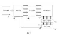
圖1為習知的一種LED顯示裝置的電路方塊圖。如圖1所示,習知的LED顯示裝置的架構包括:耦接外部的一主機處理器6a的一微控制器1a、一位元栓鎖器2a、一移位暫存器3a、一驅動電流(或定電流)產生器4a、以及一LED顯示面板5a。目前,由於LED顯示裝置的各個組成單元皆採模組化設計,因此,市面上也已經販售有所述驅動電流產生器4a的積體電路晶片,其英文名稱為:Constant-current LED sink driver。當然,市面上也有販售同時整合該位元栓鎖器2a、該移位暫存器3a、與該驅動電流產生器4a的積體電路晶片,其稱為LED顯示面板驅動晶片。Fig. 1 is a circuit block diagram of a conventional LED display device. As shown in FIG. 1, the structure of the conventional LED display device includes: a
圖2為習知的驅動電流產生器的電路方塊圖,且圖3為習知的驅動電流產生器的電路拓樸圖。如圖2與圖3所示,習知的驅動電流產生器4a的電路架構主要包括:一基準電流產生單元41a、一電流鏡像單元42a和一驅動電流產生單元43a。其中,該電流鏡像單元42a包括一第一P型電晶體421a、一第二P型電晶體、‧‧‧、和一第NP型電晶體42Na。並且,該基準電流產生單元41a包括一第一運算放大器411a、該第一電晶體元件421a、及透過一外置電阻連接腳位412a連接的一外置電阻413a。另一方面,該驅動電流產生單元43a包括一第二運算放大器430a、一第一N型電晶體431a、一第二N型電晶體、‧‧‧ 、和一第MP型電晶體43Ma。FIG. 2 is a circuit block diagram of a conventional driving current generator, and FIG. 3 is a circuit topology diagram of a conventional driving current generator. As shown in FIGS. 2 and 3, the circuit structure of the conventional driving
該第一運算放大器411a、該第一電晶體元件421a、與該外置電阻413a共同構成一負反饋系統,使得該基準電流產生單元41a所輸出的基準電流I0可由式(1):


就電流鏡像單元42a而言,其內部的每個P型電晶體(421a, …,42Na)的尺寸會被設計成相同,如此便可以基準電流I0與第一電流I1之間的比例便由所述P型電晶體(421a, …,42Na)的數量來決定。同樣的,第一電流I1與輸出電流Iout之間的比例也是所述N型電晶體(431a, …,43Ma)的數量來決定。然而,必須考慮到的是,MOSFET電晶體為一種半導體元件,而由半導體材料製成的電子元件必定受到製程誤差的影響而於電氣特性上造成變異或飄移。就電流鏡像單元42a而言,任兩個P型電晶體之間的閥值電壓失配會造成第一電流I1失配。其中,等效失配電流與P型電晶體的汲極電流的比值可由下式(5)推算。
其中,

由上述說明可知,習知的驅動電流產生器(Constant-current LED sink driver)4a具有以下實務應用上的缺陷:It can be seen from the above description that the conventional constant-current
(1)需要額外設置一個外置電阻連接腳位412a以連接的外置電阻413a,造成電路晶片的成本增加。(1) It is necessary to additionally provide an external
(2)僅能透過P型電晶體(421a, …,42Na)的數量及/或N型電晶體(431a, …,43Ma)的數量和外置電阻413a的電阻值來決定驅動電流產生器4a的輸出電流Iout的值,這對於電流的調變控制上顯然並不夠彈性。(2) The drive
(3)如前所述,在調變所述輸出電流Iout之時,電流鏡的汲極電流失配失配也會跟著一起調變,造成電路的不穩定。(3) As mentioned above, when the output current Iout is modulated, the mismatch of the drain current of the current mirror will also be modulated along with it, resulting in circuit instability.
因此,本領域亟需一種驅動電流供應電路。Therefore, there is an urgent need for a driving current supply circuit in the art.
本發明之一目的在於提供無需使用任何外置電阻來設置基準電流的驅動電流供應電路,因此減少了一個晶片腳位,降低了使用成本。An object of the present invention is to provide a driving current supply circuit that does not need to use any external resistor to set the reference current, thereby reducing one chip pin and reducing the use cost.
本發明之另一目的在於通過一內置電阻來設置基準電流的值,可以明顯的降低驅動電流供應電路的功耗。Another object of the present invention is to set the value of the reference current through a built-in resistor, which can significantly reduce the power consumption of the driving current supply circuit.
本發明之再一目的在於通過存寫寄存器的方式,使用一第一數位控制碼和一第二數位控制碼來控制驅動電流供應電路,以因應不同的適應場合而將輸出電流調變控制在0.5 mA ~ 20mA。Another object of the present invention is to use a first digital control code and a second digital control code to control the drive current supply circuit by storing and writing the register, so as to control the output current modulation to 0.5 according to different application situations. mA ~ 20mA.
本發明之又一目的令驅動電流供應電路之基準電流的產生及各電流鏡單元所貢獻的電流失配為恆定,不會依據輸出電流的調變範圍而跟著改變。Another object of the present invention is to make the generation of the reference current of the drive current supply circuit and the current mismatch contributed by each current mirror unit constant, and will not change according to the output current adjustment range.
為達成上述目的,本發明提出一種驅動電流供應電路,其包括:To achieve the above objective, the present invention provides a driving current supply circuit, which includes:
一基準電流產生單元,其耦接一第一參考電壓,用以基於該第一參考電壓而產生一基準電流;A reference current generating unit coupled to a first reference voltage for generating a reference current based on the first reference voltage;
一數位控制電流鏡單元,耦接該基準電流產生單元、一第一數位控制碼和一第二數位控制碼,並基於該第一數位控制碼和該第二數位控制碼的控制將該基準電流轉換成一第一電流;以及A digital control current mirror unit is coupled to the reference current generation unit, a first digital control code and a second digital control code, and the reference current is controlled based on the control of the first digital control code and the second digital control code Converted into a first current; and
一驅動電流產生單元,耦接該數位控制電流鏡單元以接收該第一電流,並將該第一電流轉換成一輸出電流。A drive current generating unit is coupled to the digital control current mirror unit to receive the first current and convert the first current into an output current.
在一實施例中,該數位控制電流鏡單元包括:In an embodiment, the digitally controlled current mirror unit includes:
一第一數位控制電流鏡,耦接該基準電流產生單元,用以依據一第一數位控制碼而對該基準電流進行第一次電流轉換處理,且包括一第一P型金氧半場效電晶體、2N-1個第二P型金氧半場效電晶體和2N-1個第一開關;其中,該第一P型金氧半場效電晶體的閘極與源極分別耦接該基準電流產生單元與一源極耦接一工作電壓,各所述第二P型金氧半場效電晶體的閘極耦接該第一P型金氧半場效電晶體的閘極,各所述第二P型金氧半場效電晶體的源極耦接該工作電壓;其中,各所述第一開關具有一第一電性端、一第二電性端、與一第一訊號接收端,各所述第一電性端對應耦接各所述第二P型金氧半場效電晶體的汲極,各所述第二電性端耦接第一P型金氧半場效電晶體的汲極,且該第一訊號接收端用以接收該第一數位控制碼;及A first digital control current mirror, coupled to the reference current generation unit, for performing a first current conversion process on the reference current according to a first digital control code, and includes a first P-type metal oxide half field effect voltage Crystal, 2N -1 second P-type MOSFET and 2N -1 first switch; wherein the gate and source of the first P-type MOSFET are respectively coupled to the The reference current generating unit and a source are coupled to a working voltage, the gate of each second P-type MOSFET is coupled to the gate of the first P-type MOSFET, and each of the The source of the second P-type MOSFET is coupled to the operating voltage; wherein each of the first switches has a first electrical terminal, a second electrical terminal, and a first signal receiving terminal, Each of the first electrical terminals is correspondingly coupled to the drain of each of the second P-type MOSFET, and each of the second electrical terminals is coupled to the drain of the first P-type MOSFET. Pole, and the first signal receiving terminal is used to receive the first digital control code; and
一第二數位控制電流鏡,耦接該第一數位控制電流鏡,用以依據一第二數位控制碼而對已完成所述第一次電流轉換處理的該基準電流進一步地進行第二次電流轉換處理,並輸出一第一電流;該第二數位控制電流鏡包括一第三P型金氧半場效電晶體、2M-1個第四P型金氧半場效電晶體和2M-1個第二開關;其中,各所述第四P型金氧半場效電晶體的閘極耦接該第二P型金氧半場效電晶體的閘極,各所述第四P型金氧半場效電晶體的源極耦接該工作電壓;各所述第二開關具有一第三電性端、一第四電性端、與一第二訊號接收端,各所述第三電性端對應耦接各所述第四P型金氧半場效電晶體的汲極,各所述第四電性端耦接第三P型金氧半場效電晶體的汲極,且該第二訊號接收端用以接收該第二數位控制碼;該第三P型金氧半場效電晶體的閘極與源極分別耦接所述第四P型金氧半場效電晶體的閘極和該工作電壓;以及A second digital control current mirror, coupled to the first digital control current mirror, for performing a second current on the reference current that has completed the first current conversion process according to a second digital control code Convert and process, and output a first current; the second digitally controlled current mirror includes a third P-type MOSFET, 2M -1 fourth P-type MOSFET and 2M -1 A second switch; wherein the gate of each of the fourth P-type MOSFET is coupled to the gate of the second P-type MOSFET, and each of the fourth P-type MOSFET The source of the effect transistor is coupled to the operating voltage; each of the second switches has a third electrical terminal, a fourth electrical terminal, and a second signal receiving terminal, each of the third electrical terminals corresponding to Each of the fourth electrical terminals is coupled to the drain of each of the fourth P-type MOSFETs, and each of the fourth electrical terminals is coupled to the drain of the third P-type MOSFETs, and the second signal receiving terminal For receiving the second digital control code; the gate and source of the third P-type MOSFET are respectively coupled to the gate of the fourth P-type MOSFET and the operating voltage; as well as
一驅動電流產生單元,耦接該數位控制電流鏡單元以接收該第一電流,並將該第一電流轉換成一輸出電流。A driving current generating unit is coupled to the digital control current mirror unit to receive the first current and convert the first current into an output current.
在一實施例中,該第一數位控制碼為一二進位碼,且該第二數位控制碼為一溫度計碼。In one embodiment, the first digital control code is a binary code, and the second digital control code is a thermometer code.
在一實施例中,該第一參考電壓由一帶隙參考電壓産生單元所提供。In one embodiment, the first reference voltage is provided by a band gap reference voltage generating unit.
在一實施例中,該基準電流產生單元包括:In an embodiment, the reference current generating unit includes:
一第一運算放大器,以其負輸入端與輸出端分別耦接該第一參考電壓和該第一P型金氧半場效電晶體的閘極;以及A first operational amplifier whose negative input terminal and output terminal are respectively coupled to the first reference voltage and the gate electrode of the first P-type metal oxide semi-field effect transistor; and
一內置電阻,其一端耦接該第一運算放大器的正輸入端,且其另一端耦接至一電路地端。A built-in resistor, one end of which is coupled to the positive input terminal of the first operational amplifier, and the other end of which is coupled to a circuit ground.
在一實施例中,該驅動電流產生單元包括:In an embodiment, the driving current generating unit includes:
一第二運算放大器,以其負輸入端與輸出端分別耦接一第二參考電壓和該第三P型金氧半場效電晶體的汲極;以及A second operational amplifier whose negative input terminal and output terminal are respectively coupled to a second reference voltage and the drain of the third P-type MOSFET; and
一電流鏡單元,包括一第一N型金氧半場效電晶體與一第二N型金氧半場效電晶體;其中,該第一N型金氧半場效電晶體的閘極與汲極分別耦接該第二運算放大器的輸出端與正輸入端,且該第一N型金氧半場效電晶體的源極耦接該電路地端;該第二N型金氧半場效電晶體的閘極與源極分別耦接該第一N型金氧半場效電晶體的閘極與該電路地端,且該第二N型金氧半場效電晶體的汲極作為所述驅動電流供應電路之一電流輸出端。A current mirror unit, including a first N-type MOSFET and a second N-type MOSFET; wherein the gate and drain of the first N-type MOSFET are respectively The output terminal and the positive input terminal of the second operational amplifier are coupled, and the source of the first N-type MOSFET is coupled to the circuit ground; the gate of the second N-type MOSFET The electrode and the source are respectively coupled to the gate of the first N-type MOSFET and the circuit ground, and the drain of the second N-type MOSFET is used as the driving current supply circuit A current output terminal.
在一實施例中,該第一運算放大器與該第二運算放大器皆為一誤差放大器。In one embodiment, the first operational amplifier and the second operational amplifier are both error amplifiers.
另外,本發明進一步提出一種LED顯示驅動裝置,其具有至少一組如前所述之驅動電流供應電路。In addition, the present invention further provides an LED display driving device, which has at least one set of driving current supply circuits as described above.
在可能的實施例中,該LED顯示驅動裝置更包括:In a possible embodiment, the LED display driving device further includes:
一微控制器,耦接外部的一主機處理器;A microcontroller, coupled to an external host processor;
至少一位元栓鎖器,耦接該微控制器,且各所述位元栓鎖器對應地耦接至一個LED顯示面板;At least one bit latch, coupled to the microcontroller, and each of the bit latches is correspondingly coupled to an LED display panel;
至少一移位暫存器,耦接該微控制器;以及At least one shift register coupled to the microcontroller; and
其中,各所述驅動電流供應電路對應地耦接於各所述移位暫存器和各所述LED顯示面板之間。Wherein, each of the driving current supply circuits is correspondingly coupled between each of the shift registers and each of the LED display panels.
再者,本發明又提出一種LED顯示裝置,其包括:Furthermore, the present invention provides an LED display device, which includes:
至少一LED顯示面板;At least one LED display panel;
至少一位元栓鎖器,對應地耦接至所述至少一LED顯示面板;At least one-bit latch, correspondingly coupled to the at least one LED display panel;
一微控制器,耦接所述至少一位元栓鎖器;A microcontroller coupled to the at least one-bit latch;
至少一組如前所述之驅動電流供應電路,其中各所述驅動電流供應電路對應地耦接於各所述位元栓鎖器和各所述LED顯示面板之間;以及At least one set of driving current supply circuits as described above, wherein each of the driving current supply circuits is correspondingly coupled between each of the bit latches and each of the LED display panels; and
至少一移位暫存器,耦接於該微控制器,且各所述移位暫存器對應地耦接各所述驅動電流供應電路。At least one shift register is coupled to the microcontroller, and each of the shift registers is correspondingly coupled to each of the driving current supply circuits.
為使 貴審查委員能進一步瞭解本發明之結構、特徵、目的、與其優點,茲附以圖式及較佳具體實施例之詳細說明如後。In order to enable your reviewer to further understand the structure, features, purpose, and advantages of the present invention, the drawings and detailed descriptions of preferred embodiments are attached as follows.
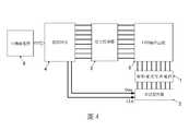
請參閱圖4,其顯示包含本發明之一種驅動電流供應電路的一LED顯示裝置的電路方塊圖。如圖4所示,LED顯示裝置的架構包括:耦接外部的一主機處理器6的一微控制器4、至少一位元栓鎖器3、至少一移位暫存器2、至少一本發明之驅動電流供應電路1、以及至少一LED顯示面板5。於此,所謂“至少一”指的是其數量為一個或一個以上。通常,一個LED顯示裝置會包含多個LED顯示面板5,因此,對應於該LED顯示面板5的設置數量,所述位元栓鎖器3、所述移位暫存器2、以及本發明之驅動電流供應電路1的數量也必須與LED顯示面板5的數量相同。易於理解的,模組化設計有助於LED顯示裝置的產線組裝與測試。因此,實務上可以將一組位元栓鎖器3、一組移位暫存器2、與一組本發明之驅動電流供應電路1整合成單一積體電路晶片,其稱為LED顯示驅動晶片。進一步地,一組LED顯示驅動晶片還可以與一組LED顯示面板5整合成一個LED顯示面板模組。Please refer to FIG. 4, which shows a circuit block diagram of an LED display device including a driving current supply circuit of the present invention. As shown in FIG. 4, the structure of the LED display device includes: a
圖5為本發明之驅動電流供應電路的電路方塊圖。本發明之驅動電流供應電路1主要包括一基準電流產生單元11、一數位控制電流鏡單元12、以及一驅動電流產生單元13。該基準電流產生單元11耦接一第一參考電壓VREF,用以基於該第一參考電壓VREF而產生一基準電流I0。並且,該數位控制電流鏡單元12耦接該基準電流產生單元11、一第一數位控制碼DR和一第二數位控制碼DI,並基於該第一數位控制碼DR和該第二數位控制碼DI的控制將該基準電流I0轉換成一第一電流I1。該驅動電流產生單元13,如圖5所示,其耦接該數位控制電流鏡單元12以接收該第一電流I1,並將該第一電流I1轉換成一輸出電流Iout。FIG. 5 is a circuit block diagram of the driving current supply circuit of the present invention. The driving
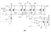
繼續地參閱圖5 ,並請同時參閱圖6,其為本發明之的驅動電流供應電路的電路拓樸圖。由圖6可知,該基準電流產生單元11主要包括一第一運算放大器111和一內置電阻112,該第一運算放大器111的負輸入端耦接一第一參考電壓VREF。並且,該內置電阻112的一端耦接該第一運算放大器111的正輸入端,且其另一端耦接至一電路地端。補充說明的是,該第一參考電壓VREF由一帶隙參考電壓産生單元所提供,且該帶隙參考電壓産生單元可以整合於本發明之驅動電流供應電路1之中,也可以是獨立的一個外部電路單元。Continue to refer to FIG. 5, and also refer to FIG. 6, which is a circuit topology diagram of the driving current supply circuit of the present invention. It can be seen from FIG. 6 that the reference
該數位控制電流鏡單元12包括一第一數位控制電流鏡121與一第二數位控制電流鏡122;其中,第一數位控制電流鏡121耦接該基準電流產生單元11,且包括一第一P型金氧半場效電晶體1210、2N-1個第二P型金氧半場效電晶體1211和2N-1個第一開關1212。必須特別說明的是,該第一運算放大器111、該內置電阻112和該第一P型金氧半場效電晶體1210組成一負反饋系統。在此負反饋系統的作用下,基準電流產生單元11係基於式(6):
依據本發明之設計,第一數位控制電流鏡121係基於一第一數位控制碼DR的控制而對該基準電流I0進行第一次電流轉換處理。如圖6所示,於所述第一數位控制電流鏡121的架構中,該第一P型金氧半場效電晶體1210的閘極與源極分別耦接該基準電流產生單元11與一源極耦接一工作電壓VDD。並且,各所述第二P型金氧半場效電晶體1211的閘極耦接該第一P型金氧半場效電晶體1210的閘極,且各所述第二P型金氧半場效電晶體1211的源極耦接該工作電壓VDD。另一方面,各所述第一開關1212具有一第一電性端、一第二電性端、與一第一訊號接收端;其中,各所述第一電性端對應耦接各所述第二P型金氧半場效電晶體1211的汲極,各所述第二電性端耦接第一P型金氧半場效電晶體1210的汲極,且該第一訊號接收端用以接收該第一數位控制碼DR。According to the design of the present invention, the first digital control
再者,該第二數位控制電流鏡122耦接該第一數位控制電流鏡121,用以依據一第二數位控制碼DI而對已完成所述第一次電流轉換處理的該基準電流I0進一步地進行第二次電流轉換處理,最終輸出一第一電流I1。如圖6所示,該第二數位控制電流鏡122包括一第三P型金氧半場效電晶體1220、2M-1個第四P型金氧半場效電晶體1221和2M-1個第二開關1222。依據本發明之設計,各所述第四P型金氧半場效電晶體1221的閘極耦接該第二P型金氧半場效電晶體1211的閘極,且各所述第四P型金氧半場效電晶體1221的源極耦接該工作電壓VDD。另一方面,各所述第二開關1222具有一第三電性端、一第四電性端、與一第二訊號接收端;其中,各所述第三電性端對應耦接各所述第四P型金氧半場效電晶體1221的汲極,各所述第四電性端耦接第三P型金氧半場效電晶體1220的汲極,且該第二訊號接收端用以接收該第二數位控制碼DI。補充說明的是,該第三P型金氧半場效電晶體1220的閘極與源極分別耦接所述第四P型金氧半場效電晶體1221的閘極和該工作電壓VDD。Furthermore, the second digitally controlled
簡單地說,第一數位控制電流鏡121包含2N個P型MOSFET與2N-1個第一開關1212,且所述2N-1個第一開關1212係受控於第一數位控制碼DR。並且,第二數位控制電流鏡122包含2M個P型MOSFET與2M-1個第二開關1222,且所述2M-1個第二開關1222係受控於第二數位控制碼DI。特別地,本發明令該第一數位控制碼DR與該第二數位控制碼DI分別為一二進位碼和一溫度計碼。如此設計,則基準電流I0與第一電流I1之間的比值便可以由下式(7)所決定。
繼續地參閱圖5與圖6。該驅動電流產生單元13耦接該數位控制電流鏡單元12的該第二數位控制電流鏡122以接收所述第一電流I1,並將該第一電流I1轉換成一輸出電流Iout。該驅動電流產生單元13包括一第二運算放大器131和一電流鏡單元132。於本發明中,該第一運算放大器111與該第二運算放大器131皆為一誤差放大器。並且,如圖6所示,該第二運算放大器131以其負輸入端與輸出端分別耦接一第二參考電壓VCRES和該第三P型金氧半場效電晶體1220的汲極。另一方面,該電流鏡單元132包括一第一N型金氧半場效電晶體1321與一第二N型金氧半場效電晶體1322;其中,該第一N型金氧半場效電晶體1321的閘極與汲極分別耦接該第二運算放大器131的輸出端與正輸入端,且該第一N型金氧半場效電晶體1321的源極耦接該電路地端。再者,該第二N型金氧半場效電晶體1322的閘極與源極分別耦接該第一N型金氧半場效電晶體1321的閘極與該電路地端,且該第二N型金氧半場效電晶體1322的汲極作為所述驅動電流供應電路之一電流輸出端。Continue to refer to Figures 5 and 6. The driving
電流鏡單元132以電流比值(Current ratio)K對第一電流I1進行所述電流轉換處理,因此驅動電流產生單元13最終輸出的輸出電流

由上式(6)已知可透過設置該內置電阻112的阻值以決定基準電流I0的值;接著,透過第一數位控制碼DR、第二數位控制碼DI和電流鏡單元132的電流比值(Current ratio)K可以最終決定此驅動電流供應電路1的輸出電流Iout的值。It is known from the above formula (6) that the value of the reference current I0 can be determined by setting the resistance of the built-in
值得特別說明的是,第一數位控制電流鏡121與第二數位控制電流鏡122包括多個單位電流源,且各個單位電流源之中的金氧半場效電晶體都被操作在飽和區。在這種情況下,各個單位電流源的電流失配主要來自於金氧半場效電晶體的閥值電壓(或稱臨界電壓)的失配。對於每個金氧半場效電晶體而言,其等效失配電流與汲極電流的比可由下式(9)計算:
其中,

易於理解的,在輸出電流Iout為恆定的情況下,只要金氧半場效電晶體的元件長度L不變,則每個金氧半場效電晶體的等效失配電流與汲極電流的比


如此,上述係已完整且清楚地說明本發明之驅動電流供應電路、LED顯示驅動裝置及LED顯示裝置;並且,經由上述可得知本發明係具有下列之優點:In this way, the above system has completely and clearly explained the driving current supply circuit, LED display driving device and LED display device of the present invention; and from the above, it can be seen that the present invention has the following advantages:
(1)本發明之驅動電流供應電路1無需使用任何外置電阻來設置基準電流I0的值,因此減少了一個晶片腳位,降低了使用成本。(1) The drive
(2)本發明之驅動電流供應電路1 通過內置電阻112來設置基準電流I0的值,可以明顯的降低此驅動電流供應電路1的功耗。(2) The drive
(3)本發明通過 第一數位控制碼DR和第二數位控制碼DI控制數位控制電流鏡單元12,以因應不同的適應場合而將本發明之驅動電流供應電路1的輸出電流Iout調變控制在0.5 mA ~ 20mA;亦即,本發明之驅動電流供應電路1可以通過存寫寄存器的方式達到簡易調整輸出電流Iout之效果。(3) The present invention controls the digital control
(4)依據本發明之設計,基準電流I0的產生及第一數位控制電流鏡121和第二數位控制電流鏡122所貢獻的電流失配為恆定,不會依據輸出電流Iout的調變範圍而跟著改變。(4) According to the design of the present invention, the generation of the reference current I0 and the current mismatch contributed by the first digitally controlled
必須加以強調的是,前述本案所揭示者乃為較佳實施例,舉凡局部之變更或修飾而源於本案之技術思想而為熟習該項技藝之人所易於推知者,俱不脫本案之專利權範疇。It must be emphasized that the foregoing disclosures in this case are preferred embodiments, and any partial changes or modifications that are derived from the technical ideas of this case and are easily inferred by those who are familiar with the art will not deviate from the patent of this case. Right category.
綜上所陳,本案無論目的、手段與功效,皆顯示其迥異於習知技術,且其首先發明合於實用,確實符合發明之專利要件,懇請 貴審查委員明察,並早日賜予專利俾嘉惠社會,是為至禱。In summary, regardless of the purpose, means and effect of this case, it is shown that it is very different from the conventional technology, and its first invention is suitable for practicality, and it does meet the patent requirements of the invention. I sincerely ask the examiner to check it out and grant the patent as soon as possible. Society is for the best prayer.
<本發明>1:驅動電流供應電路2:移位暫存器3:位元栓鎖器4:微控制器5:LED顯示面板6:主機處理器11:基準電流產生單元12:數位控制電流鏡單元13:驅動電流產生單元111:第一運算放大器112:內置電阻121:第一數位控制電流鏡122:第二數位控制電流鏡1210:第一P型金氧半場效電晶體1211:第二P型金氧半場效電晶體1212:第一開關1220:第三P型金氧半場效電晶體1221:第四P型金氧半場效電晶體1222:第二開關131:第二運算放大器132:電流鏡單元1321:第一N型金氧半場效電晶體1322:第二N型金氧半場效電晶體<The present invention>1: Drive current supply circuit2: shift register3: bit latch4: Microcontroller5: LED display panel6: host processor11: Reference current generation unit12: Digital control current mirror unit13: Drive current generating unit111: The first operational amplifier112: Built-in resistance121: The first digital control current mirror122: The second digital control current mirror1210: The first P-type metal oxide half field effect transistor1211: The second P-type metal oxide half field effect transistor1212: First switch1220: The third P-type metal oxide half field effect transistor1221: The fourth P-type metal oxide half field effect transistor1222: second switch131: second operational amplifier132: Current mirror unit1321: The first N-type metal oxide half field effect transistor1322: The second N-type metal oxide half field effect transistor
<習知>6a:主機處理器1a:微控制器2a:位元栓鎖器3a:移位暫存器4a:驅動電流產生器5a:LED顯示面板<Acquaintances>6a:
圖1為習知的一種LED顯示裝置的電路方塊圖; 圖2為習知的驅動電流產生器的電路方塊圖; 圖3為習知的驅動電流產生器的電路拓樸圖; 圖4為包含本發明之一種驅動電流供應電路的一LED顯示裝置的電路方塊圖; 圖5為本發明之驅動電流供應電路的電路方塊圖;以及 圖6為本發明之的驅動電流供應電路的電路拓樸圖。Fig. 1 is a circuit block diagram of a conventional LED display device; Fig. 2 is a circuit block diagram of a conventional drive current generator; Fig. 3 is a circuit topology diagram of a conventional drive current generator; A circuit block diagram of an LED display device of a driving current supply circuit of the present invention; FIG. 5 is a circuit block diagram of the driving current supply circuit of the present invention; and FIG. 6 is a circuit topology diagram of the driving current supply circuit of the present invention .
1:驅動電流供應電路1: Drive current supply circuit
11:基準電流產生單元11: Reference current generation unit
12:數位控制電流鏡單元12: Digital control current mirror unit
13:驅動電流產生單元13: Drive current generating unit
Claims (9)
Translated fromChinesePriority Applications (1)
| Application Number | Priority Date | Filing Date | Title |
|---|---|---|---|
| TW108114735ATWI699747B (en) | 2019-04-26 | 2019-04-26 | Drive current supply circuit, LED display drive device and LED display device |
Applications Claiming Priority (1)
| Application Number | Priority Date | Filing Date | Title |
|---|---|---|---|
| TW108114735ATWI699747B (en) | 2019-04-26 | 2019-04-26 | Drive current supply circuit, LED display drive device and LED display device |
Publications (2)
| Publication Number | Publication Date |
|---|---|
| TWI699747Btrue TWI699747B (en) | 2020-07-21 |
| TW202040546A TW202040546A (en) | 2020-11-01 |
Family
ID=72601956
Family Applications (1)
| Application Number | Title | Priority Date | Filing Date |
|---|---|---|---|
| TW108114735ATWI699747B (en) | 2019-04-26 | 2019-04-26 | Drive current supply circuit, LED display drive device and LED display device |
Country Status (1)
| Country | Link |
|---|---|
| TW (1) | TWI699747B (en) |
Cited By (1)
| Publication number | Priority date | Publication date | Assignee | Title |
|---|---|---|---|---|
| CN113870772A (en)* | 2021-10-19 | 2021-12-31 | 中科芯集成电路有限公司 | Light intensity control and trimming circuit and control method for transparent flexible screen lamp bead |
Families Citing this family (2)
| Publication number | Priority date | Publication date | Assignee | Title |
|---|---|---|---|---|
| TWI807725B (en)* | 2022-03-25 | 2023-07-01 | 大陸商北京集創北方科技股份有限公司 | Trimming circuit, LED display driver chip and LED display device |
| TWI807724B (en)* | 2022-03-25 | 2023-07-01 | 大陸商北京集創北方科技股份有限公司 | Trimming circuit, LED display driver chip, and LED display device |
Citations (6)
| Publication number | Priority date | Publication date | Assignee | Title |
|---|---|---|---|---|
| US20020060524A1 (en)* | 2000-07-26 | 2002-05-23 | Kim Hak Su | Current control circuit for display device |
| TW200421239A (en)* | 2003-03-24 | 2004-10-16 | Nec Electronics Corp | Current drive circuit and display |
| TW200506791A (en)* | 2003-08-06 | 2005-02-16 | Ind Tech Res Inst | Current drive system with high uniformity reference current and its current driver |
| US20070211043A1 (en)* | 2006-03-07 | 2007-09-13 | Oki Electric Industry Co., Ltd. | Current drive circuit |
| TW200929149A (en)* | 2007-12-31 | 2009-07-01 | Au Optronics Corp | Liquid crystal display apparatus and bandgap reference circuit thereof |
| CN102881251A (en)* | 2012-08-20 | 2013-01-16 | 深圳市易事达电子股份有限公司 | Current drive circuit |
- 2019
- 2019-04-26TWTW108114735Apatent/TWI699747B/enactive
Patent Citations (6)
| Publication number | Priority date | Publication date | Assignee | Title |
|---|---|---|---|---|
| US20020060524A1 (en)* | 2000-07-26 | 2002-05-23 | Kim Hak Su | Current control circuit for display device |
| TW200421239A (en)* | 2003-03-24 | 2004-10-16 | Nec Electronics Corp | Current drive circuit and display |
| TW200506791A (en)* | 2003-08-06 | 2005-02-16 | Ind Tech Res Inst | Current drive system with high uniformity reference current and its current driver |
| US20070211043A1 (en)* | 2006-03-07 | 2007-09-13 | Oki Electric Industry Co., Ltd. | Current drive circuit |
| TW200929149A (en)* | 2007-12-31 | 2009-07-01 | Au Optronics Corp | Liquid crystal display apparatus and bandgap reference circuit thereof |
| CN102881251A (en)* | 2012-08-20 | 2013-01-16 | 深圳市易事达电子股份有限公司 | Current drive circuit |
Cited By (1)
| Publication number | Priority date | Publication date | Assignee | Title |
|---|---|---|---|---|
| CN113870772A (en)* | 2021-10-19 | 2021-12-31 | 中科芯集成电路有限公司 | Light intensity control and trimming circuit and control method for transparent flexible screen lamp bead |
Also Published As
| Publication number | Publication date |
|---|---|
| TW202040546A (en) | 2020-11-01 |
Similar Documents
| Publication | Publication Date | Title |
|---|---|---|
| TWI699747B (en) | Drive current supply circuit, LED display drive device and LED display device | |
| TWI474751B (en) | Led current control circuits and methods | |
| CN201623900U (en) | A driving circuit for parallel light-emitting diodes | |
| CN102548114B (en) | Light emitting diode driving device | |
| US8077139B2 (en) | Driving circuit of backlight module | |
| JP2006319057A (en) | Light emitting diode drive circuit | |
| CN102402948A (en) | Light-emitting element array driving circuit and current distribution circuit and method used therein | |
| CN202257349U (en) | Current generating circuit | |
| CN109036269B (en) | Pixel circuit, pixel driving method and organic electroluminescence display device | |
| CN100481716C (en) | Bias circuit and control circuit thereof | |
| JP7659057B2 (en) | Power supply circuits, chips and displays | |
| US8471478B2 (en) | Light control signal generating circuit | |
| CN116229857B (en) | A constant current source drive control system for digital tubes | |
| CN115334708B (en) | LED drive circuit, LED control circuit, chip and electronic equipment | |
| CN102395234B (en) | Low voltage CMOS constant current source circuit with high matching degree | |
| CN101562933B (en) | Driving circuit of backlight module | |
| CN115985255B (en) | Current drive device and display device | |
| CN102159009B (en) | White light LED (light-emitted diode)-line pulse dimming circuit | |
| TWI762090B (en) | Constant current source generating circuit, LED display driver chip, LED display device, and information processing device | |
| CN215773653U (en) | Single-wire three-channel high-power LED drive control module | |
| TWI806704B (en) | Driver circuit, LED display driver chip and information processing device | |
| CN215935137U (en) | Drive circuit and lighting apparatus | |
| TWI868975B (en) | Pixel circuit | |
| TWI806705B (en) | Driver circuit, LED display driver chip and information processing device | |
| CN115171589B (en) | Driving circuit and display device |